WO2012002151A1 - 液晶装置 - Google Patents
液晶装置 Download PDFInfo
- Publication number
- WO2012002151A1 WO2012002151A1 PCT/JP2011/063678 JP2011063678W WO2012002151A1 WO 2012002151 A1 WO2012002151 A1 WO 2012002151A1 JP 2011063678 W JP2011063678 W JP 2011063678W WO 2012002151 A1 WO2012002151 A1 WO 2012002151A1
- Authority
- WO
- WIPO (PCT)
- Prior art keywords
- liquid crystal
- pixel
- capacitor
- potential
- switching element
- Prior art date
- Legal status (The legal status is an assumption and is not a legal conclusion. Google has not performed a legal analysis and makes no representation as to the accuracy of the status listed.)
- Ceased
Links
Images










Classifications
-
- G—PHYSICS
- G09—EDUCATION; CRYPTOGRAPHY; DISPLAY; ADVERTISING; SEALS
- G09G—ARRANGEMENTS OR CIRCUITS FOR CONTROL OF INDICATING DEVICES USING STATIC MEANS TO PRESENT VARIABLE INFORMATION
- G09G3/00—Control arrangements or circuits, of interest only in connection with visual indicators other than cathode-ray tubes
- G09G3/20—Control arrangements or circuits, of interest only in connection with visual indicators other than cathode-ray tubes for presentation of an assembly of a number of characters, e.g. a page, by composing the assembly by combination of individual elements arranged in a matrix no fixed position being assigned to or needed to be assigned to the individual characters or partial characters
- G09G3/34—Control arrangements or circuits, of interest only in connection with visual indicators other than cathode-ray tubes for presentation of an assembly of a number of characters, e.g. a page, by composing the assembly by combination of individual elements arranged in a matrix no fixed position being assigned to or needed to be assigned to the individual characters or partial characters by control of light from an independent source
- G09G3/36—Control arrangements or circuits, of interest only in connection with visual indicators other than cathode-ray tubes for presentation of an assembly of a number of characters, e.g. a page, by composing the assembly by combination of individual elements arranged in a matrix no fixed position being assigned to or needed to be assigned to the individual characters or partial characters by control of light from an independent source using liquid crystals
- G09G3/3611—Control of matrices with row and column drivers
- G09G3/3648—Control of matrices with row and column drivers using an active matrix
- G09G3/3659—Control of matrices with row and column drivers using an active matrix the addressing of the pixel involving the control of two or more scan electrodes or two or more data electrodes, e.g. pixel voltage dependant on signal of two data electrodes
-
- G—PHYSICS
- G09—EDUCATION; CRYPTOGRAPHY; DISPLAY; ADVERTISING; SEALS
- G09G—ARRANGEMENTS OR CIRCUITS FOR CONTROL OF INDICATING DEVICES USING STATIC MEANS TO PRESENT VARIABLE INFORMATION
- G09G3/00—Control arrangements or circuits, of interest only in connection with visual indicators other than cathode-ray tubes
- G09G3/20—Control arrangements or circuits, of interest only in connection with visual indicators other than cathode-ray tubes for presentation of an assembly of a number of characters, e.g. a page, by composing the assembly by combination of individual elements arranged in a matrix no fixed position being assigned to or needed to be assigned to the individual characters or partial characters
- G09G3/34—Control arrangements or circuits, of interest only in connection with visual indicators other than cathode-ray tubes for presentation of an assembly of a number of characters, e.g. a page, by composing the assembly by combination of individual elements arranged in a matrix no fixed position being assigned to or needed to be assigned to the individual characters or partial characters by control of light from an independent source
- G09G3/36—Control arrangements or circuits, of interest only in connection with visual indicators other than cathode-ray tubes for presentation of an assembly of a number of characters, e.g. a page, by composing the assembly by combination of individual elements arranged in a matrix no fixed position being assigned to or needed to be assigned to the individual characters or partial characters by control of light from an independent source using liquid crystals
- G09G3/3611—Control of matrices with row and column drivers
- G09G3/3648—Control of matrices with row and column drivers using an active matrix
- G09G3/3651—Control of matrices with row and column drivers using an active matrix using multistable liquid crystals, e.g. ferroelectric liquid crystals
-
- G—PHYSICS
- G02—OPTICS
- G02F—OPTICAL DEVICES OR ARRANGEMENTS FOR THE CONTROL OF LIGHT BY MODIFICATION OF THE OPTICAL PROPERTIES OF THE MEDIA OF THE ELEMENTS INVOLVED THEREIN; NON-LINEAR OPTICS; FREQUENCY-CHANGING OF LIGHT; OPTICAL LOGIC ELEMENTS; OPTICAL ANALOGUE/DIGITAL CONVERTERS
- G02F1/00—Devices or arrangements for the control of the intensity, colour, phase, polarisation or direction of light arriving from an independent light source, e.g. switching, gating or modulating; Non-linear optics
- G02F1/01—Devices or arrangements for the control of the intensity, colour, phase, polarisation or direction of light arriving from an independent light source, e.g. switching, gating or modulating; Non-linear optics for the control of the intensity, phase, polarisation or colour
- G02F1/13—Devices or arrangements for the control of the intensity, colour, phase, polarisation or direction of light arriving from an independent light source, e.g. switching, gating or modulating; Non-linear optics for the control of the intensity, phase, polarisation or colour based on liquid crystals, e.g. single liquid crystal display cells
- G02F1/133—Constructional arrangements; Operation of liquid crystal cells; Circuit arrangements
- G02F1/1333—Constructional arrangements; Manufacturing methods
- G02F1/1343—Electrodes
- G02F1/134309—Electrodes characterised by their geometrical arrangement
- G02F1/134345—Subdivided pixels, e.g. for grey scale or redundancy
-
- G—PHYSICS
- G09—EDUCATION; CRYPTOGRAPHY; DISPLAY; ADVERTISING; SEALS
- G09G—ARRANGEMENTS OR CIRCUITS FOR CONTROL OF INDICATING DEVICES USING STATIC MEANS TO PRESENT VARIABLE INFORMATION
- G09G2300/00—Aspects of the constitution of display devices
- G09G2300/04—Structural and physical details of display devices
- G09G2300/0439—Pixel structures
- G09G2300/0443—Pixel structures with several sub-pixels for the same colour in a pixel, not specifically used to display gradations
-
- G—PHYSICS
- G09—EDUCATION; CRYPTOGRAPHY; DISPLAY; ADVERTISING; SEALS
- G09G—ARRANGEMENTS OR CIRCUITS FOR CONTROL OF INDICATING DEVICES USING STATIC MEANS TO PRESENT VARIABLE INFORMATION
- G09G2300/00—Aspects of the constitution of display devices
- G09G2300/04—Structural and physical details of display devices
- G09G2300/0469—Details of the physics of pixel operation
- G09G2300/0478—Details of the physics of pixel operation related to liquid crystal pixels
- G09G2300/0495—Use of transitions between isotropic and anisotropic phases in liquid crystals, by voltage controlled deformation of the liquid crystal molecules, as opposed to merely changing the orientation of the molecules as in, e.g. twisted-nematic [TN], vertical-aligned [VA], cholesteric, in-plane, or bi-refringent liquid crystals
-
- G—PHYSICS
- G09—EDUCATION; CRYPTOGRAPHY; DISPLAY; ADVERTISING; SEALS
- G09G—ARRANGEMENTS OR CIRCUITS FOR CONTROL OF INDICATING DEVICES USING STATIC MEANS TO PRESENT VARIABLE INFORMATION
- G09G2300/00—Aspects of the constitution of display devices
- G09G2300/08—Active matrix structure, i.e. with use of active elements, inclusive of non-linear two terminal elements, in the pixels together with light emitting or modulating elements
- G09G2300/0809—Several active elements per pixel in active matrix panels
-
- G—PHYSICS
- G09—EDUCATION; CRYPTOGRAPHY; DISPLAY; ADVERTISING; SEALS
- G09G—ARRANGEMENTS OR CIRCUITS FOR CONTROL OF INDICATING DEVICES USING STATIC MEANS TO PRESENT VARIABLE INFORMATION
- G09G2320/00—Control of display operating conditions
- G09G2320/02—Improving the quality of display appearance
- G09G2320/0233—Improving the luminance or brightness uniformity across the screen
-
- G—PHYSICS
- G09—EDUCATION; CRYPTOGRAPHY; DISPLAY; ADVERTISING; SEALS
- G09G—ARRANGEMENTS OR CIRCUITS FOR CONTROL OF INDICATING DEVICES USING STATIC MEANS TO PRESENT VARIABLE INFORMATION
- G09G2320/00—Control of display operating conditions
- G09G2320/02—Improving the quality of display appearance
- G09G2320/0238—Improving the black level
Definitions
- the present invention relates to a liquid crystal device.
- This application claims priority based on Japanese Patent Application No. 2010-147646 filed in Japan on June 29, 2010, the contents of which are incorporated herein by reference.
- a glass substrate used for a panel of a liquid crystal device is manufactured by a float method, a fusion method or the like.
- a glass substrate produced by a fusion method which is a kind of pulling-down method, has no damage to the surface due to physical contact during production unlike the float method. Therefore, the glass substrate manufactured by the fusion method has high surface accuracy, but has a higher manufacturing cost than the float method.
- the glass substrate manufactured by the float process is a flat glass continuously formed by flowing molten glass on molten metal tin and utilizing the molten tin surface. Although the glass substrate manufactured by the float process has a lower manufacturing cost than the fusion process, thickness unevenness due to fine waviness as shown in FIG. 25 can be formed on the surface.
- FIG. 25 thickness unevenness due to fine waviness due to fine waviness as shown in FIG. 25 can be formed on the surface.
- the liquid crystal panel includes a spacer 921 in the liquid crystal layer 911 between the glass substrate 901 and the glass substrate 902 facing each other in order to keep the cell thickness uniform.
- the liquid crystal collects in the lower part of the liquid crystal device due to the weight when the liquid crystal device is erected after the liquid crystal device is assembled. Due to local pressurization during assembly, some of the spacers 921 are crushed, resulting in uneven cell thickness.
- FIG. 26 is a diagram illustrating a state where a voltage is not applied to the liquid crystal 911 (dark display state) when a VA (Vertical Alignment) liquid crystal device is driven in a normally black mode.
- FIG. 27 is a diagram for explaining a state where a voltage is applied to the liquid crystal 911 when the VA liquid crystal device is driven in a normally black mode (bright display state).
- the transmittance of the liquid crystal layer 911 between the glass substrate 901 and the glass substrate 902 facing each other is I / I o . expressed.
- the relationship between I and Io is expressed as the following equation (1).
- I is the radiation divergence of incident light.
- I o is the radiant divergence of light that has passed through the liquid crystal.
- ⁇ n is a birefringence (also referred to as refractive index anisotropy) rate (in the case of liquid crystal, for example, 0.08).
- d is the cell thickness.
- ⁇ is the wavelength of transmitted light.
- ⁇ is the tilt angle of the liquid crystal 911.
- sin 2 (2 ⁇ ) 1 because ⁇ is structurally set to 45 degrees. For this reason, Formula (1) is represented like following Formula (2).
- FIG. 28 is a diagram for explaining the characteristics of applied voltage versus transmittance due to the difference in cell thickness. As shown in FIG. 28, when the cell thickness is increased, the birefringence phase difference ⁇ n ⁇ d (retardation) is increased, and the light transmittance is increased.
- Patent Document 1 requires a large-capacity memory for storing correction data and a large-scale correction circuit, which increases costs. Furthermore, in the prior art of Patent Document 1, it is necessary to actually measure the display state for each liquid crystal device in order to create data for unevenness correction, which requires a data creation process. In addition, in order to correct unevenness with high accuracy, it is necessary to generate correction data by acquiring a large amount of fine measurement data in a three-dimensional direction with respect to space and gradation. For this reason, it becomes a big burden with respect to cost or productivity.
- An object of one embodiment of the present invention is to provide a liquid crystal device that corrects luminance unevenness due to cell thickness unevenness.
- a liquid crystal device includes a first substrate over which a first pixel having a nonlinear element and a pixel electrode is formed, and a second substrate facing the first substrate.
- the first substrate includes a substrate, a liquid crystal layer between the first substrate and the second substrate, and a mechanism for changing the potential of the pixel electrode based on the thickness of the liquid crystal layer.
- the mechanical unit boosts the potential of the pixel electrode when the thickness of the liquid crystal layer decreases, and increases the thickness of the liquid crystal layer.
- the potential of the pixel electrode may be lowered.
- the liquid crystal device is a normally black mode liquid crystal device, and further includes a display signal line for supplying a display signal and a common electrode.
- the pixel has a liquid crystal capacitor, and the mechanism for changing the potential of the pixel electrode is the pixel electrode connected to the liquid crystal capacitor after writing the liquid crystal capacitor by applying a potential from the display signal line.
- the first potential difference between the first potential difference and the common electrode is smaller than the second potential difference between the display signal line and the common electrode, and the polarity of the variation in the difference in the second potential difference with respect to the first potential difference is the liquid crystal.
- the capacitance may be varied so as to be opposite to the polarity of the variation in the thickness of the liquid crystal layer.
- the first pixel includes a plurality of subpixels, and at least one of the plurality of subpixels includes a first gate, a source, and a drain electrode.
- a liquid crystal display comprising: a first switching element having a second switching element having a second gate, a source and a drain electrode; a first scanning line; a second scanning line; and a first capacitor.
- One of the capacitors is connected to the second drain electrode and the first drain electrode, the other of the liquid crystal capacitor is connected to the common electrode, and the second source electrode is connected to the display signal line,
- the second gate electrode is connected to the first scanning line, the first source electrode is connected to one end of the first capacitor, and the other end of the first capacitor is connected to an auxiliary capacitor electrode.
- the first The gate electrode is connected to the second scanning line, and the mechanism for changing the potential of the pixel electrode selects the first scanning line, and then selects the second scanning line to thereby select the pixel.
- the potential of the electrode may be changed.
- each of the plurality of subpixels may be capacitively coupled to at least one other subpixel.
- the liquid crystal device further includes second and third pixels, the second pixel includes a second capacitor, and the third pixel includes a third capacitor.
- the second and third pixels may correspond to RGB pixels, and the first, second, and third capacitors may have different capacities.
- the present invention it is possible to correct luminance unevenness due to cell thickness unevenness when the liquid crystal device performs display.
- FIG. 1 is a perspective view illustrating a schematic configuration of a liquid crystal device according to an embodiment of the present invention. It is a block diagram of an example of the liquid crystal device to which the embodiment of the present invention is applied. It is a figure explaining the state at the time of L frame of the equivalent circuit at the time of nth pixel selection in the liquid crystal device concerning a 1st embodiment.
- FIG. 7 is a diagram for explaining a state at the time of L + 1 frame of an equivalent circuit when an nth pixel is selected in the liquid crystal device according to the same embodiment.
- 4 is a timing chart of the liquid crystal device according to the embodiment. It is a figure explaining the example of the layout on the 1st glass substrate 3 which concerns on the same embodiment.
- FIG. 10 is a simplified representation of the equivalent circuit of FIG. 9 according to the embodiment.
- FIG. 4 is a timing chart of a liquid crystal device including two subpixels according to the embodiment. It is a figure explaining the example of the layout on the 1st glass substrate 3 which concerns on the same embodiment. It is an example of the equivalent circuit at the time of n-th pixel selection in a liquid crystal device provided with two subpixels concerning 3rd Embodiment.
- FIG. 14 is a simplified representation of the equivalent circuit of FIG. 13 according to the embodiment.
- 4 is a timing chart of a liquid crystal device including two subpixels according to the embodiment. It is a figure explaining the example of the layout on the 1st glass substrate 3 which concerns on the same embodiment.
- FIG. 18 is a simplified representation of the equivalent circuit of FIG. 17 according to the embodiment.
- 4 is a timing chart of a liquid crystal device including three subpixels according to the embodiment.
- FIG. 21 is a simplified representation of the equivalent circuit of FIG. 20 according to the same embodiment. It is an example of the equivalent circuit at the time of nth pixel selection in a liquid crystal device provided with four subpixels concerning 6th Embodiment.
- FIG. 18 is a simplified representation of the equivalent circuit of FIG. 17 according to the embodiment.
- 4 is a timing chart of a liquid crystal device including three subpixels according to the embodiment.
- FIG. 21 is a simplified representation of the equivalent circuit of FIG. 20 according to the same embodiment.
- FIG. 22 is a simplified representation of the equivalent circuit of FIG. 21 according to the embodiment.
- 4 is a timing chart of a liquid crystal device including four sub-pixels according to the embodiment. It is sectional drawing of the liquid crystal panel in the liquid crystal device which concerns on a prior art. It is a figure explaining the state (dark display state) to which the voltage is not applied to the liquid crystal 911 when driving the liquid crystal device of the VA system which concerns on a prior art in normally black mode. It is a figure explaining the state (bright display state) to which the voltage is applied to the liquid crystal 911 in the case of driving the VA-type liquid crystal device which concerns on a prior art in normally black mode. It is a figure explaining the characteristic of the applied voltage versus the transmittance
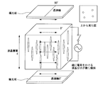
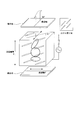
- FIG. 1 is a perspective view illustrating a schematic configuration of the liquid crystal device according to the present embodiment.
- the liquid crystal device includes a backlight 1, a first polarizing plate 2, a first glass substrate 3, a TFT (thin film transistor) array 4, a liquid crystal 5, a common electrode (counter electrode) 6, A color filter 7, a second glass substrate 8, and a second polarizing plate 9 are provided.
- the backlight 1 emits light from below the first glass substrate 3.
- the first polarizing plate 2 controls light input / output to / from the first glass substrate 3 by polarization.
- a TFT array 4 in which switching elements, pixel electrodes and the like are formed is disposed on the first glass substrate 3.
- the first substrate includes a first glass substrate 3 and a TFT array 4.
- a liquid crystal 5 is sealed between the pixel electrode of the TFT array 4 and the common electrode 6.
- the color filter 7 is disposed on the common electrode 6, and filters each of RGB and applies light based on the light reflectance or light transmittance of the liquid crystal corresponding to each controlled pixel as RGB colors on the liquid crystal device. Is displayed.
- the second glass substrate 8 is disposed on the color filter 7, and the second polarizing plate 9 disposed in crossed Nicols (crossed Nicols) with the first polarizing plate 2 is disposed on the second glass substrate 8. ing.
- the second substrate includes a common electrode 6 and a second glass substrate 8.
- FIG. 2 is a configuration diagram of an example of a liquid crystal device to which the embodiment of the present invention is applied.
- the liquid crystal device includes a control unit 21 and a pixel unit 22.
- the pixel unit 22 includes m display signal lines (data bus lines) 11-1 to 11-m, n scanning lines (gate bus lines) 12-1 to 12-n, and n ⁇ m pixels. (P (1,1) to p (1, m), p (2,1) to p (2, m)... P (n, 1) to p (n, m)).
- the control unit 21 transmits the pixels p (1,1) to p (1, m), p (2,1) via the display signal lines 11-1 to 11-m and the scanning lines 12-1 to 12-n. To p (2, m)... P (n, 1) to p (n, m).
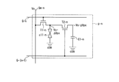
- FIG. 3 is a diagram for explaining the state of the equivalent circuit in the L frame when the nth pixel is selected in the liquid crystal device according to this embodiment.
- FIG. 4 is a diagram for explaining a state in the L + 1 frame of the equivalent circuit when the nth pixel is selected in the liquid crystal device according to the present embodiment.
- 3 to 8 show the configuration and operation of one pixel pn.
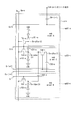
- the configuration of the pixel pn will be described with reference to FIG.
- the gate electrode of the switching element T1-n is connected to the scanning line GN.
- the source electrode of the switching element T1-n (second switching element) is connected to the display signal line Sm-n.
- the drain electrode of the switching element T1-n is connected to one of the liquid crystal capacitors cl1-n having a capacitive component and the drain electrode of the switching element T2-n via a pixel electrode.
- the other of the liquid crystal capacitors cl1-n is grounded (sometimes referred to as “com”) through the common electrode 6. That is, the liquid crystal capacitor cl1-n is sandwiched between the common electrode 6 and the pixel electrode.
- the source electrode of the switching element T2-n (first switching element) is connected to one terminal of the first self-compensation capacitor C1-n (first capacitor). The other terminal of the first self-compensation capacitor C1-n is grounded. Further, the gate electrode of the switching element T2-n is connected to the scanning line G- (n + 1). That is, in the first embodiment, the capacitance of the pixel pn is formed by the liquid crystal capacitance cl1-n and the first self-compensation capacitance C1-n.
- the switching element is, for example, a TFT (Thin Film Transistor).
- the mechanism for changing the potential of the pixel electrode is constituted by the switching element T2-n (first switching element) and the first self-compensation capacitor C1-n (first capacitor).
- the scanning line connected to the gate electrode of the switching element T2-n may not be the scanning line G- (n + 1).
- the scanning line connected to the gate electrode of the switching element T2-n may be a scanning line subsequent to the pixel pn, such as G- (n + 2) or G- (n + 3).
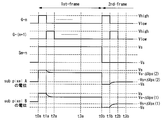
- FIG. 5 is a timing chart of the liquid crystal device according to this embodiment.
- the control unit 21 controls the signal of the display signal line Sm-n to ⁇ Vs, thereby supplying ⁇ Vs from the display signal line Sm-n to the source electrode of the switching element T1-n of the pixel pn (FIG. 5, time t0a).
- the control unit 21 controls the signal of the scanning line Gn to the H level (high potential level, sometimes referred to as “Vhigh”) during the period from time t1a to t2a (rewriting period for one pixel).
- the switching element T1-n is turned on, and the potential ⁇ Vs is supplied to the liquid crystal capacitor cl1-n from the display signal line Sm-n. Therefore, the potential ⁇ Vs is generated in the liquid crystal capacitor cl1-n as shown in FIGS.
- the period during which the output of the scanning line Gn is at the H level corresponds to, for example, 1 / (60 ⁇ 1080) (seconds) in a Full-HD compatible liquid crystal device.
- the signal range of the display signal line Sm-n when displaying the maximum gradation from the zero gradation is + Vs to -Vs, for example, a positive potential +5 V to +1 V, and a negative potential -5 V. ⁇ -1V. This signal level may be adjusted to the characteristics of the liquid crystal capacitance used.
- the control unit 21 controls the scanning line G- (n + 1) to the L level (low potential level; sometimes referred to as “Vlow”) to turn off the switching element T2-n. Put it in a state. Therefore, the first self-compensation capacitor C1-n holds the potential Vx when the switching element T2-n is in the on state in the immediately preceding frame.
- the control unit 21 controls the scanning line Gn to the L level to turn off the switching element T1-n (FIG. 5, time t2a).
- the potential + Vs of the display signal line Sm-n is supplied (FIG. 5, time t3a).
- the switching element T2-n is turned on by controlling the scanning line G- (n + 1) to H level (FIG. 5, time t4a). Since the switching element T2-n connected to the liquid crystal capacitor cl1-n of the pixel pn is in the on state, the charge held in the liquid crystal capacitor cl1-n is connected to the source electrode of the switching element T2-n.
- the control unit 21 controls the switching elements T1-n to T2-n to be in an off state, so that the potential at the time t5a is next to the liquid crystal capacitor cl1-n of the pixel pn. Holds up to L + 1 frames.
- the capacitance of the liquid crystal capacitor cl1-n is C LC
- the capacitance of the first self-compensation capacitor C1-n is C down
- the potential V pn of the liquid crystal capacitor cl1 -n is expressed by the following equation (3 ).
- ⁇ is the dielectric constant
- Sp ⁇ n is the area of the pixel electrode.
- the voltage applied to the liquid crystal depends on the ratio between the liquid crystal capacitance cl1-n and the first self-compensation capacitance C1-n. As the cell thickness d of the liquid crystal increases, the liquid crystal capacitance cl1-n decreases and becomes smaller than the self-compensation capacitance C1-n, so the voltage decreases. In the normally black mode, the voltage drop becomes the brightness drop. In the conventional technique, the luminance increases as the cell thickness d increases.
- the capacitance that balances the increase in luminance and the decrease in luminance due to voltage drop As the first self-compensation capacitor C1-n, it is possible to compensate for luminance unevenness due to an increase in cell thickness d. Further, when the cell thickness d of the liquid crystal is decreased, the liquid crystal capacitance cl1-n is increased, and the voltage is increased because it is larger than the self-compensation capacitance C1-n. In the normally black mode, an increase in voltage results in an increase in luminance. In the conventional technique, the luminance decreases as the cell thickness d decreases. By setting a capacitance that balances the luminance decrease and the luminance increase due to the voltage increase as the first self-compensation capacitor C1-n, it is possible to compensate for luminance unevenness due to the decrease in the cell thickness d.
- the control unit 21 supplies the potential ⁇ Vs to the display signal line Sm-n (FIG. 5, FIG. 5). Time t0a). Next, the control unit 21 controls the scanning line Gn to H level to turn on the switching element T1-n, and writes the potential ⁇ Vs to the liquid crystal capacitor Cl1-n during the period of time t1a to t2a.
- the thickness unevenness of the cell thickness of the liquid crystal is self-corrected.
- “increase in cell thickness d” means that the cell thickness d is larger than a certain reference thickness.
- “reduction in cell thickness d” means that the cell thickness d is smaller than a certain reference thickness. That is, in the liquid crystal device, even when the cell thickness is different for each pixel formed at a different position, the occurrence of luminance unevenness can be suppressed.
- the control unit 21 supplies the display signal line Sm-n with the potential + Vs having the opposite polarity to the L frame (FIG. 5, time t0b). Therefore, a potential + Vs opposite to that in the L frame is generated in the liquid crystal capacitor cl1-n of the pixel pn. That is, even in the L + 1 frame, the control unit 21 writes the potential + Vs to the liquid crystal capacitor cl1-n by controlling the switching element T1-n to be in the on state during the period of time t1b to t2b.
- the control unit 21 turns off the switching element T1-n, and then supplies the potential ⁇ Vs to the display signal line Sm-n (FIG. 5, time t3b).
- the control unit 21 turns on the switching element T2-n, so that the potential of the liquid crystal capacitor cl1-n of the pixel pn decreases by ⁇ Vpx based on the first self-compensation capacitor C1-n, and + Vs To + Vs ⁇ Vpx.
- one frame is 1/60 second in a liquid crystal device driven at 60 Hz, for example.
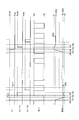
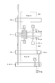
- FIG. 6 is a diagram for explaining an example of the layout on the first glass substrate 3 in the present embodiment.
- the scanning lines Gn to G- (n + 1), the switching elements T1-n to T2-n, the com wiring, and the pixels An electrode 101 and a first self-compensation capacitor C1-n are formed.
- the pixel electrode 101 is connected to the drain electrode of the switching element T1-n and the drain electrode of the switching element T2-n.
- the gate electrode of the switching element T1-n is connected to the scanning line GN.
- the gate electrode of the switching element T2-n is connected to the scanning line G- (n + 1).
- One of the first self-compensation capacitors C1-n is connected to the source electrode of the switching element T2-n.
- the other of the first self-compensation capacitors C1-n is formed so as to be connected to the com wiring and grounded.
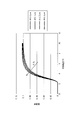
- the horizontal axis shows an example of gradations 0 to 256 gradations.
- each self-compensation capacitor is designed such that the potential of the pixel electrode is 0.94 times the potential of the display signal line Sm-n.
- the control unit 21 writes a potential to the sub-pixel electrode constituting the liquid crystal capacitor cl1-n of the pixel. Thereafter, the control unit 21 controls the switching element T2-n connected to the first self-compensation capacitor C1-n, and varies the charge of the liquid crystal capacitor cl1-n by the first self-compensation capacitor C1-n. Thereby, luminance unevenness due to the cell thickness of the liquid crystal can be reduced. Further, the method according to the present embodiment is effective in, for example, a VA (Vertical Alignment) type and IPS (In-Plane Switching) type liquid crystal device adopting a normally black mode.
- VA Very Alignment
- IPS In-Plane Switching
- FIG. 9 is a diagram for explaining a matrix configuration of liquid crystal capacitors in the present embodiment.
- a plurality of pixels are arranged in a matrix, and each pixel includes two sub-pixels (sometimes referred to as “sub pixel”).
- the pixel p (1, 1) includes a sub pixel sp (1, 1, 1) and a sub pixel sp (2, 1, 1).
- FIG. 10 is an example of an equivalent circuit when the nth pixel is selected in the liquid crystal device according to the present embodiment.
- the pixel pn includes two subpixels sp21-n and sp22-n.
- the subpixels sp21-n and sp22-n are arranged adjacent to each other in the column direction.
- Each subpixel includes a liquid crystal capacitor, a switching element on the pixel electrode, and a common electrode portion facing the pixel electrode.
- the liquid crystal capacitor has a liquid crystal material sandwiched between a common electrode facing one pixel electrode.
- the liquid crystal capacitance is expressed as an electric capacitance as an electric equivalent circuit.
- the configuration of the pixel pn will be described with reference to FIG.
- the gate electrode of the switching element T21-n of the subpixel sp21-n (second switching element) is connected to the scanning line GN.
- the source electrode of the switching element T21-n is connected to the display signal line Sm-n.
- the drain electrode of the switching element T21-n is connected to one of the liquid crystal capacitors cl21-n having a capacitance component and the source electrode of the switching element T22-n (first switching element) via the pixel electrode.
- the other terminal of the liquid crystal capacitor cl21-n is grounded through the common electrode 6. That is, the liquid crystal capacitor cl21-n is sandwiched between the common electrode 6 and the pixel electrode.
- the drain electrode of the switching element T22-n is connected to one terminal of the first self-compensation capacitor C21-n (first capacitor). The other terminal of the first self-compensation capacitor C21-n is grounded. Further, the gate electrode of the switching element T22-n is connected to the scanning line G- (n + 1). The gate electrode of the switching element T23-n (second switching element) of the sub-pixel sp22-n is connected to the scanning line GN. The source electrode of the switching element T23-n is connected to the display signal line Sm-n.
- the drain electrode of the switching element T23-n is connected to one of the liquid crystal capacitors cl22-n having a capacitance component and the source electrode of the switching element T24-n (first switching element) via the pixel electrode.
- the other terminal of the liquid crystal capacitor cl22-n is grounded through the common electrode 6. That is, the liquid crystal capacitor cl22-n is sandwiched between the common electrode 6 and the pixel electrode.
- the drain electrode of the switching element T24-n is connected to one terminal of the second self-compensation capacitor C22-n (first capacitor).
- the other terminal of the second self-compensation capacitor C22-n is grounded.
- the gate electrode of the switching element T24-n is connected to the scanning line G- (n + 1).
- the mechanism for changing the potential of the pixel electrode is constituted by the switching element T22-n (first switching element) and the first self-compensation capacitor C21-n (first capacitor).
- the mechanism for changing the potential of the pixel electrode includes a switching element T24-n (first switching element) and a second self-compensation capacitor C22-n (first capacitor).
- the scanning line connected to the gate electrode of the switching element T22-n and the gate electrode of the switching element T24-n may not be the scanning line G- (n + 1), but a scanning line subsequent to the pixel pn, for example, G- (n + 2) or G- (n + 3) may be used.
- FIG. 11 is a timing chart of the liquid crystal device according to this embodiment.
- the control unit 21 controls the signal of the display signal line Sm-n to ⁇ Vs, thereby displaying on the switching element T21-n and the source electrode of the switching element T23-n of each of the subpixels sp21-n to sp22-n. -Vs is supplied from the signal line Sm-n. (FIG. 11, time t0a).
- the control unit 21 turns on the switching elements T21-n and T23-n by controlling the signal of the scanning line Gn to the H level during the period from time t1a to t2a (rewriting period for one pixel).
- the potential ⁇ Vs is supplied from the display signal line Sm-n to the liquid crystal capacitors cl21-n and cl22-n. Therefore, a potential ⁇ Vs is generated between the pixel electrode constituting the liquid crystal capacitor cl21-n and the pixel electrode constituting the liquid crystal capacitor cl22-n.
- the period during which the output of the scanning line Gn is at the H level corresponds to, for example, 1 / (60 ⁇ 1080) (seconds) in a Full-HD compatible liquid crystal device.
- the signal range of the display signal line Sm-n when displaying the maximum gradation from the zero gradation is + Vs to -Vs, for example, a positive potential +5 V to +1 V, and a negative potential -5 V. ⁇ -1V.
- This signal level may be adjusted to the characteristics of the liquid crystal capacitance used.
- the control unit 21 controls the scanning line G- (n + 1) to the L level, thereby turning off the switching element T22-n and the switching element T24-n. Therefore, the first self-compensation capacitor C21-n and the second self-compensation capacitor C22-n include the switching element T22-n and the switching element T24-n when they are in the on state in the immediately preceding frame. The potential Vx is held.
- the control unit 21 controls the scanning line Gn to L level to turn off the switching element T21-n and the switching element T23-n (FIG. 11, time t2a).
- the potential + Vs of the display signal line Sm-n is supplied (FIG. 11, time t3a).
- the scanning line G- (n + 1) is controlled to the H level, so that the switching element T22-n and the switching element T24-n are turned on (FIG. 11, time t4a).
- the switching element T22-n connected to the liquid crystal capacitor cl21-n of the sub-pixel sp21-n is in an on state, the charge held in the liquid crystal capacitor cl21-n is connected to the source electrode of the switching element T22-n.
- the first self-compensation capacitor C21-n is moved. Therefore, the potential of the liquid crystal capacitor cl21-n increases by ⁇ Vpx (1) based on the first self-compensation capacitor C21-n, and changes from ⁇ Vs to ⁇ Vs + ⁇ Vpx (1).
- the switching element T24-n connected to the liquid crystal capacitor cl22-n of the sub-pixel sp22-n is in an on state, the charge held in the liquid crystal capacitor cl22-n is changed to the source electrode of the switching element T24-n. Move to the second self-compensation capacitor C22-n connected to. For this reason, the potential of the pixel electrode constituting the liquid crystal capacitor cl22-n rises by ⁇ Vpx (2) based on the second self-compensation capacitor C22-n and changes from ⁇ Vs to ⁇ Vs + ⁇ Vpx (2).
- control unit 21 controls the switching elements T21-n to T24-n to be in an off state, thereby causing the liquid crystal capacitors cl21-n to cl22-n of the sub-pixels sp21-n to sp22-n.
- the potential at time t5a is held until the next L + 1 frame.
- the control unit 21 supplies the display signal line Sm-n with the potential + Vs having the opposite polarity to the L frame (FIG. 11, time t0b). Even in the L + 1 frame, the control unit 21 controls the switching element T21-n and the switching element T23-n to be in the on state during the period from time t1b to time t2b. Therefore, a potential + Vs opposite to that in the L frame is generated in the pixel electrodes constituting the liquid crystal capacitors cl21 to cl22-n of the subpixels sp21-n to sp22-n.
- the control unit 21 turns off the switching element T21-n and the switching element T23-n, and then supplies the potential ⁇ Vs to the display signal line Sm-n (FIG. 11, time t3b).
- the control unit 21 turns on the switching element T22-n during the period from time t3b to time t4b, so that the potential of the pixel electrode constituting the liquid crystal capacitor cl21-n of the subpixel sp21-n becomes the first.
- the voltage drops by ⁇ Vpx (1) and changes from + Vs to + Vs ⁇ Vpx (1).
- control unit 21 turns on the switching element T24-n during the period from time t3b to time t4b, so that the potential of the pixel electrode constituting the liquid crystal capacitor cl22-n of the subpixel sp22-n becomes the second self Based on the compensation capacitance C22-n, the voltage decreases by ⁇ Vpx (2) and changes from + Vs to + Vs ⁇ Vpx (2). Note that one frame is 1/60 second in a liquid crystal device driven at 60 Hz, for example.
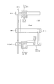
- FIG. 12 is a diagram for explaining an example of the layout on the first glass substrate 3 in the present embodiment.
- the scanning lines Gn to G- (n + 1), the switching elements T21-n to T24-n, the com wiring, and the pixel Electrodes 201 and 202, a first self-compensation capacitor C21-n, and a second self-compensation capacitor C22-n are formed.
- the pixel electrode 201 is connected to the drain electrode of the switching element T21-n and the drain electrode of the switching element T22-n.
- the gate electrode of the switching element T21-n is connected to the scanning line GN.
- the gate electrode of the switching element T22-n is connected to the scanning line G- (n + 1).
- One of the first self-compensation capacitors C21-n is connected to the source electrode of the switching element T22-n.
- the other of the first self-compensation capacitors C21-n is formed so as to be connected to the com wiring.
- the drain electrode of the switching element T23-n and the drain electrode of the switching element T24-n are connected to the pixel electrode 202.
- the gate electrode of the switching element T23-n is connected to the scanning line G-na.
- the gate electrode of the switching element T24-n is connected to the scanning line G- (n + 1).
- One of the second self-compensation capacitors C22-n is connected to the source electrode of the switching element T24-n.
- the other of the second self-compensation capacitors C22-n is formed to be connected to the com wiring. Note that the same signal is applied to the scanning line G-n and the scanning line G-na at the same timing.
- the control unit 21 writes a potential in the liquid crystal capacitor cl21-n of the sub-pixel sp21-n. Thereafter, the control unit 21 controls the switching element T22-n connected to the first self-compensation capacitor C1-n, and the charge of the liquid crystal capacitor cl21-n is between the first self-compensation capacitor C21-n.
- the potential difference applied to the liquid crystal capacitor cl21-n is reduced.
- the magnitude of the decrease in the potential difference suppresses the change in transmittance due to the liquid crystal cell thickness variation. That is, the magnitude of the decrease in potential difference suppresses the change in transmittance due to the liquid crystal cell thickness being different for each liquid crystal cell.
- the control unit 21 writes a potential in the liquid crystal element cl22-n of the sub-pixel sp22-n. Thereafter, the control unit 21 controls the switching element T24-n connected to the second self-compensation capacitor C22-n, and the charge of the liquid crystal capacitor cl22-n is transferred between the second self-compensation capacitor C22-n. By rearranging, the potential difference applied to the liquid crystal capacitor cl22-n is reduced. The magnitude of the decrease in the potential difference suppresses the change in transmittance due to the liquid crystal cell thickness variation.
- the magnitude of the decrease in potential difference suppresses the change in transmittance due to the liquid crystal cell thickness being different for each liquid crystal cell. Thereby, luminance unevenness due to the cell thickness of the liquid crystal can be reduced.
- the first self-compensation capacitor C21-n of the sub-pixel sp (1, 1, 1) has a large luminance variation value and low luminance unevenness that is easily noticeable as in the first embodiment. Improves brightness unevenness due to cell thickness of gradation to medium gradation.
- the second self-compensation capacitor C22-n of the sub-pixel sp (2, 1, 1) has an effect of improving luminance unevenness due to the cell thickness in other gradation regions.
- the compensation function of the sub-pixel sp21-n is operated in the low to middle gradation region and the compensation function of the sub-pixel sp22-n is operated in the middle to high gradation, the compensation is effective in a wider gradation range than the first embodiment. Further, the method according to the present embodiment is effective in, for example, a VA mode or IPS mode liquid crystal device that employs a normally black mode.
- FIG. 13 is an example of an equivalent circuit when the nth pixel is selected in a liquid crystal device including two subpixels in the present embodiment.
- 13 to 14 show the configuration of one pixel pn.
- the pixel pn includes two sub-pixels sp31-n to sp32-n.
- the subpixels sp31-n to sp32-n are arranged adjacent to each other in the column direction.
- FIG. 14 is a simplified representation of the equivalent circuit of FIG.
- Pixel electrodes denoted by reference numerals 301 to 302 are the pixel electrodes of the sub-pixels sp31-n to sp32-n.
- the pixel electrode 301 of the sub-pixel A (sp31-n) is connected to the drain electrode of the switching element T31-n and one of the first self-compensation capacitors C31-n.
- the pixel electrode 302 of the sub-pixel B (sp32-n) is connected to the drain electrode of the switching element T32-n and the other one of the first self-compensation capacitors C31-n.
- the source electrode of the switching element T33-n is connected to one terminal of the second self-compensation capacitor C32-n.
- the gate electrode of the switching element T31-n is connected to the scanning line Gn.
- the source electrode of the switching element T31-n is connected to the display signal line Sm-n.
- the drain electrode of the switching element T31-n is connected to one of the liquid crystal capacitors cl31-n having a capacitive component via the pixel electrode 301 and one terminal of the first self-compensation capacitor C31-n (second capacitor). It is connected to the.
- the other terminal of the liquid crystal capacitor cl31-n is grounded through the common electrode 6. That is, the liquid crystal capacitor cl31-n is sandwiched between the common electrode 6 and the pixel electrode 301.
- the gate electrode of the switching element T32-n (second switching element) is connected to the scanning line GN.
- the source electrode of the switching element T32-n is connected to the display signal line Sm-n.
- the drain electrode of the switching element T32-n is connected to one of the liquid crystal capacitors cl32-n having a capacitive component via the pixel electrode 302 and connected to the other terminal of the first self-compensation capacitor C31-n. It is connected to the drain electrode of T33-n (first switching element).
- the other terminal of the liquid crystal capacitor cl32-n is grounded through the common electrode 6.
- the source electrode of the switching element T33-n is connected to one terminal of the second self-compensation capacitor C32-n (first capacitor).
- the other terminal of the second self-compensation capacitor C32-n is connected to the common wiring Cs- (n + 1) (auxiliary capacitor electrode).
- the gate electrode of the switching element T33-n is connected to the scanning line G- (n + 1).
- the common wiring Cs- (n + 1) is preferably fixed at a constant potential, and may be common to Cs-n or other common wiring.
- the mechanism for changing the potential of the pixel electrode includes a switching element T33-n (first switching element), a second self-compensation capacitor C32-n (first capacitor), and a first self-compensation capacitor C31-n. (Second capacity).
- the scanning line connected to the gate electrode of the switching element T33-n may not be the scanning line G- (n + 1), but a scanning line subsequent to the pixel pix n, for example, G- (n + 2) or G- (n + 3). ) Etc.
- FIG. 15 is a timing chart of a liquid crystal device including two subpixels in the present embodiment.
- the control unit 21 controls the signal of the display signal line Sm-n to Vs, so that the display signal line is connected to each source electrode of each switching element T31 to n to T32-n of each subpixel sp31-n to sp32-n. Vs is supplied from Sm-n. (FIG. 15, time t0a).
- the control unit 21 controls the signal of the scanning line Gn to the H level (high potential level, sometimes referred to as “Vhigh”) during the period from time t0a to t1a (rewriting period for one pixel).
- the switching elements T31-n to T32-n are turned on, and the potential Vs is supplied from the display signal line Sm-n to the liquid crystal capacitors cl31-n to cl32-n. Therefore, the potential Vs is generated in the liquid crystal capacitors cl31-n to cl32-n as shown in FIG.
- the period during which the output of the scanning line Gn is at the H level is set according to the total number of scanning lines 3 used in the liquid crystal device. For example, in a full-HD compatible liquid crystal device, 1 / (60 ⁇ 1080). ) (Seconds).
- the signal range of the display signal line Sm-n when displaying the maximum gradation from the zero gradation is + Vs to -Vs, for example, a positive potential +5 V to +1 V, and a negative potential -5 V. ⁇ -1V.
- This signal level may be adjusted to the characteristics of the liquid crystal capacitance used.
- the control unit 21 controls the scanning line G- (n + 1) to L level, thereby turning off the switching element T33-n. Therefore, the second self-compensation capacitor C32-n holds the potential Vx when the switching element T33-n is in the on state in the immediately preceding frame.
- the control unit 21 controls the scanning line Gn to the L level to turn off the switching elements T31-n to T32-n.
- the control unit 21 controls the scanning line G- (n + 1) to the H level to turn on the switching element T33-n. Since the switching element 33-n connected to the liquid crystal capacitor cl32-n of the sub-pixel sp32-n is in the on state, the charge held in the liquid crystal capacitor cl32-n is connected to the source electrode of the switching element T33-n. It moves to the second self-compensation capacitor C32-n. As a result, the potential of the liquid crystal capacitor cl32-n decreases by ⁇ Vpx (1) based on the second self-compensation capacitor C32-n, and changes from Vs to Vs ⁇ Vpx (1).
- the pixel electrode 301 constituting the liquid crystal capacitor cl31-n and the pixel electrode 302 constituting the liquid crystal capacitor cl32-n are capacitively coupled by the first self-compensation capacitor C31-n. Accordingly, as a result of the potential of the pixel electrode 302 constituting the liquid crystal capacitor cl32-n of the sub-pixel sp32-n being lowered, the potential fluctuation also occurs in the pixel electrode 301 constituting the liquid crystal capacitor cl31-n. Therefore, the potential of the liquid crystal capacitor cl31-n decreases by ⁇ Vpx (2) and changes from Vs to Vs ⁇ Vpx (2).
- the relationship between the potential difference ⁇ Vpx (2) and ⁇ Vpx (1) is determined by the balance between the liquid crystal capacitor cl31-n, the liquid crystal capacitor cl32-n, the first self-compensation capacitor C31-n, and the second self-compensation capacitor C32-n. For example, each capacity is set so that ⁇ Vpx (1) is larger than ⁇ Vpx (2).
- the control unit 21 controls the switching elements T31-1 to T33-n to be in an off state, thereby causing the liquid crystal capacitors cl31-n to cl32-n of the sub-pixels sp31-n to sp32-n.
- the potential at time t2a is held until the next frame.
- the potential of the liquid crystal capacitance of each sub-pixel is such that the potential of the pixel electrode 301 constituting the liquid crystal capacitance cl31-n of the sub-pixel sp31-n is the sub-pixel. It is larger than the potential of the pixel electrode 302 constituting the liquid crystal capacitance cl32-n of sp32-n. For this reason, the light transmittance or light reflectance of each liquid crystal capacitor of each subpixel differs according to the potential difference of each liquid crystal capacitor of each subpixel.
- the entire pixel can be regarded as a combination of the gradation luminance characteristics of both sub-pixels, the characteristics of the sub-pixel sp31-n dominate in the low to medium gradation areas, and the characteristics of the sub-pixel sp32-n dominate in the medium to high gradation areas It becomes the target.
- the pixel potential varies so that self-compensation is applied to the cell thickness variation. Therefore, the compensation function of the sub-pixel sp31-n is operated in the low to middle gradation region, and the compensation function of the sub-pixel sp32-n is operated in the middle to high gradation region, so that the compensation is effective in a wider gradation range than the first embodiment. Become.
- the control unit 21 supplies the display signal line Sm-n with a potential having a polarity opposite to that at the time of the L frame, that is, ⁇ Vs. Therefore, a potential opposite to that in the L frame is generated in each of the subpixels sp31-n to sp32-n.
- the control unit 21 writes the potential ⁇ Vs by controlling the switching elements T31-n to T32-n to be in the on state during the period from time t0b to t1b.
- the control unit 21 turns off the switching elements T31-n to T32-n, and turns on the switching element T33-n during the period of time t1b to t2b. Similarly, a potential difference is generated between the sub-pixels to realize gradation expression. Note that one frame is 1/60 second in a liquid crystal device driven at 60 Hz, for example.
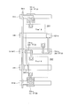
- FIG. 16 is a diagram for explaining an example of the layout on the first glass substrate 3 in the present embodiment.
- the scanning lines Gn to G- (n + 1), the switching elements T31-n to T33-n, the com wiring, and the pixel Electrodes 301 to 302, a first self-compensation capacitor C31-n, and a second self-compensation capacitor C32-n are formed.
- the drain electrode of the switching element T31-n is connected to the pixel electrode 301.
- a first self-compensation capacitor C31-n is formed between the pixel electrode 301 and the pixel electrode 302, a first self-compensation capacitor C31-n is formed.
- drain electrode of the switching element T32-n and the drain electrode of the switching element T34-n are connected to the pixel electrode 302.
- the gate electrode of the switching element T34-n is connected to the scanning line G- (n + 1).
- One of the second self-compensation capacitors C32-n is connected to the source electrode of the switching element T34-n.
- the other of the second self-compensation capacitors C32-n is formed to be connected to the com wiring.
- the gate electrode of the switching element T31-n and the gate electrode of the switching element T32-n are formed so as to be connected to the common scanning line Gn.
- the switching element T33-n connected to the scanning line G- (n + 1) to be in an on state, the potential written to the pixel electrode 302 constituting the liquid crystal capacitor cl32-n of the sub-pixel sp32-n is changed from Vs.
- the potential of the pixel electrode 301-n constituting the liquid crystal capacitor cl31-n is lowered from Vs to Vs- ⁇ Vpx (2) by capacitive coupling.
- control unit 21 writes the potential into the liquid crystal capacitors cl31-n to cl32-n of each sub-pixel, and then switches the switching element T33-n connected to the second self-compensation capacitor C32-n. Control. As a result, the potential of the liquid crystal capacitor cl32-n is changed, and further, the liquid crystal capacitor cl31-n is used by using the first self-compensation capacitor C31-n connected between the liquid crystal capacitor cl31-n and the liquid crystal capacitor cl32-n. Vary the potential. While reducing luminance unevenness due to the cell thickness of the liquid crystal, one pixel is divided into two sub-pixels to express two gradations.
- the liquid crystal capacitors cl31-n to cl32-n of all the sub-pixels sp31-n to sp32-n are connected to the display signal line Sm-n via the switching elements T31-n to T32-n. It is configured to be connected. Compared with a technique in which coupling capacitors are connected to a plurality of sub-pixels and controlled by one switching element, each liquid crystal capacitor cl31-n to cl32-n is not floated, so that there is an effect that burn-in does not occur.
- the sub-pixel sp31-n also includes a switching element and a self-compensation capacitor for changing the potential in the same manner as the sub-pixel sp32-n.
- the present embodiment since only the first self-compensation capacitor is formed between the pixel electrode 301 of the subpixel sp31-n and the pixel electrode 302 of the subpixel sp32-n, four switching elements are provided.
- the structure can be simplified, there is also an effect of suppressing the decrease in the aperture ratio.
- FIG. 17 is an example of an equivalent circuit when the nth pixel is selected in a liquid crystal device including three subpixels in the present embodiment. 17 to 18 show the configuration of one pixel pn.
- FIG. 18 is a simplified representation of the equivalent circuit of FIG.
- Pixel electrodes denoted by reference numerals 401 to 403 are pixel electrodes of the sub-pixels sp41-n to sp43-n.
- the gate electrode of the switching element T41-n of the sub-pixel sp41-n is connected to the scanning line GN.
- the source electrode of the switching element T41-n is connected to the display signal line Sm-n.
- the drain electrode of the switching element T41-n is connected to one terminal of a liquid crystal capacitor cl41-n having a capacitance component and one terminal of a first self-compensation capacitor c41-n via a pixel electrode 401.
- the other terminal of the liquid crystal capacitor cl41-n is grounded through the common electrode 6. That is, the liquid crystal capacitor cl41-n is sandwiched between the common electrode 6 and the pixel electrode 401.
- the gate electrode of the switching element T42-n is connected to the scanning line Gn.
- the source electrode of the switching element T42-n is connected to the display signal line Sm-n.
- the drain electrode of the switching element T42-n is connected to one terminal of the liquid crystal capacitor cl42-n having a capacitive component and the other terminal of the first self-compensation capacitor C41-n via the pixel electrode 402, and the second self-compensation.
- the capacitor C42-n is connected to one terminal.
- the other terminal of the liquid crystal capacitor cl42-n is grounded through the common electrode 6.
- the gate electrode of the switching element T43-n is connected to the scanning line Gn.
- the source electrode of the switching element T43-n is connected to the display signal line Sm-n.
- the drain electrode of the switching element T43-n is one of a liquid crystal capacitor cl43-n having a capacitive component via the pixel electrode 403, the other terminal of the second self-compensation capacitor C42-n, and the drain electrode of the switching element T44-n. It is connected to the.
- the other terminal of the liquid crystal capacitor cl43-n is grounded through the common electrode 6.
- the source electrode of the switching element T44-n is connected to one terminal of the third self-compensation capacitor C43-n.
- the other terminal of the third self-compensation capacitor C43-n is connected to the common wiring Cs- (n + 1) (auxiliary capacitor electrode).
- the gate electrode of the switching element T44-n is connected to the scanning line G- (n + 1).
- the mechanism for changing the potential of the pixel electrode includes a switching element T44-n (first switching element), a third self-compensation capacitor C43-n (first capacitor), and a second self-compensation capacitor C42-n. (Second capacitor) and first self-compensation capacitor C41-n (second capacitor).
- the scanning line connected to the gate electrode of the switching element T44-n may not be the scanning line G- (n + 1), but a scanning line subsequent to the pixel pn, for example, G- (n + 2) or G- ( n + 3) or the like.
- FIG. 19 is a timing chart of a liquid crystal device including three subpixels in the present embodiment.
- the control unit 21 controls the signal of the display signal line Sm-n to Vs, so that the display signal line is connected to each source electrode of each of the switching elements T41 to n to T43-n of each subpixel sp41-n to sp43-n. Vs is supplied from Sm-n. (FIG. 19, time t0a).
- the control unit 21 controls the switching elements T41-n to T43-n by controlling the signal of the scanning line Gn to the H level during the period from time t0a to t1a (rewriting period for one pixel).
- the potential Vs is supplied from the display signal line Sm-n to the liquid crystal capacitors cl41-n to cl43-n. Therefore, the potential Vs is generated in the liquid crystal capacitors cl41-n to cl43-n as shown in FIGS.
- the period during which the output of the scanning line Gn is at the H level corresponds to, for example, 1 / (60 ⁇ 1080) (seconds) in a Full-HD compatible liquid crystal device.
- the signal range of the display signal line Sm-n when displaying the maximum gradation from the zero gradation is + Vs to -Vs, for example, a positive potential +5 V to +1 V, and a negative potential -5 V. ⁇ -1V. This signal level may be adjusted to the characteristics of the liquid crystal capacitance used.
- the control unit 21 controls the scanning line G- (n + 1) to L level, thereby turning off the switching element T44-n. Therefore, the third self-compensation capacitor C43-n holds the potential Vx when the switching element T44-n is in the on state in the immediately preceding frame.
- the control unit 21 controls the scanning line Gn to L level to turn off the switching elements T41-n to T43-n, and controls the scanning line G- (n + 1) to H level to perform switching.
- the element T44-n is turned on. Since the switching element T44-n connected to the liquid crystal capacitor cl43-n of the sub-pixel sp43-n is in the on state, the charge held in the liquid crystal capacitor cl43-n is connected to the source electrode of the switching element T44-n. It moves to the third self-compensation capacitor C43-n. As a result, the potential of the liquid crystal capacitor cl43-n decreases by ⁇ Vpx (1) based on the third self-compensation capacitor C43-n, and changes from Vs to Vs ⁇ Vpx (1).
- the pixel electrode 401 constituting the liquid crystal capacitor cl41-n and the pixel electrode 402 constituting the liquid crystal capacitor cl42-n are capacitively coupled by the first self-compensating capacitor C41-n.
- the pixel electrode 402 constituting the liquid crystal capacitor cl42-n and the pixel electrode 403 constituting the liquid crystal capacitor cl43-n are capacitively coupled by the second self-compensation capacitor C42-n. Therefore, as a result of the potential of the pixel electrode 403 constituting the liquid crystal capacitor cl43-n of the sub-pixel sp43-n being lowered, the potential fluctuation also occurs in the pixel electrode 402 constituting the liquid crystal capacitor cl42-n.
- the potential of the liquid crystal capacitor cl42-n decreases by ⁇ Vpx (2) and changes from Vs to Vs ⁇ Vpx (2). Further, as a result of the potential of the pixel electrode 402 constituting the liquid crystal capacitance cl42-n of the sub-pixel sp42-n being lowered, the potential fluctuation also occurs in the pixel electrode 401 constituting the liquid crystal capacitance cl41-n. Therefore, the potential of the liquid crystal capacitor cl41-n decreases by ⁇ Vpx (3) and changes from Vs to Vs ⁇ Vpx (3).
- ⁇ Vpx (3), ⁇ Vpx (2), and ⁇ Vpx (1) is as follows: liquid crystal capacitor cl41-n, liquid crystal capacitor cl42-n, liquid crystal capacitor cl43-n, first self-compensation capacitor C41-n, and second self It is determined by the balance between the compensation capacitor C42-n and the third self-compensation capacitor C43-n.
- each capacitance is set so that the potential of ⁇ Vpx (1) is greater than the potential of ⁇ Vpx (2) and the potential of ⁇ Vpx (2) is greater than the potential of ⁇ Vpx (3). to set.
- control unit 21 controls the switching elements T41-1 to T44-n to be in an off state, thereby causing the liquid crystal capacitors cl41-n to cl43-n of the sub-pixels sp41-n to sp43-n.
- the potential at time t2a is held until the next frame.
- the magnitude of the potential of the liquid crystal capacitance of each sub-pixel is as follows.
- the potential of the pixel electrode 401 constituting the liquid crystal capacitor cl41-n of the subpixel sp41-n is higher than the potential of the pixel electrode 402 constituting the liquid crystal capacitor cl42-n of the subpixel sp42-n.
- the potential of the pixel electrode 402 constituting the liquid crystal capacitance cl42-n of the subpixel sp42-n is higher than the potential of the pixel electrode 403 constituting the liquid crystal capacitance cl43-n of the subpixel sp43-n.
- the light transmittance or light reflectance of each liquid crystal capacitor of each subpixel differs according to the potential difference of each liquid crystal capacitor of each subpixel.
- the entire pixel can be regarded as a combination of the gradation luminance characteristics of the three sub-pixels. Accordingly, the characteristics of the sub-pixel sp41-n are dominant in the low gradation region. In the middle gradation region, the characteristics of the sub-pixel sp42-n are dominant. In the high gradation region, the characteristics of the sub-pixel sp43-n are dominant.
- the pixel potential fluctuates so that self-compensation is applied to the cell thickness variation, so that the sub-pixel sp41-n in the low gradation region, the sub-pixel sp42-n in the middle gradation region, In the adjustment area, the compensation function of the sub-pixel sp43-n operates. Thereby, compensation is effective in a wider gradation range than in the first embodiment and the second embodiment.
- the operation in the L + 1 frame is after time t0b in FIG. 19, and the control unit 21 supplies the display signal line Sm-n with a potential having a polarity opposite to that in the L frame, that is, ⁇ Vs. For this reason, a potential opposite to that in the L frame is generated in each of the sub pixels sp41-n to sp43-n.
- the control unit 21 writes the potential ⁇ Vs by controlling the switching elements T41-n to T43-n to be in the on state during the period from the time t0b to t1b.
- the control unit 21 turns off the switching elements T41-n to T43-n and turns on the switching element T44-n during the time t1b to t2b, so that Similarly, a potential difference is generated between the sub-pixels to realize gradation expression.
- one frame is 1/60 second in a liquid crystal device driven at 60 Hz, for example.
- the areas of the pixel electrodes 401 to 403 of the sub-pixels sp41-n to sp43-n may all be the same, for example.
- the area of the pixel electrode 401: the area of the pixel electrode 402: the area of the pixel electrode 403 may be 1: 1.5: 2.
- the potential of the pixel 401 constituting the liquid crystal capacitor cl41-n is lowered from Vs to Vs ⁇ Vpx (3) by capacitive coupling. For this reason, the larger the liquid crystal capacitance cl43-n to which the switching element T44-n is connected, the easier it is to lower the liquid crystal capacitance cl42-n and the liquid crystal capacitance cl41-n, and it functions at a high gradation in view angle characteristics. A larger pixel area is desirable.
- the control unit 21 writes a potential in each of the liquid crystal capacitors cl41-n to cl43-n of each subpixel. Thereafter, by controlling the switching element T44-n connected to the third self-compensation capacitor C43-n, the potential of the liquid crystal capacitor cl43-n is changed, and further, the liquid crystal capacitor cl42-n and the liquid crystal capacitor cl43-n are changed.
- the potential of the liquid crystal capacitor cl42-n is changed by using the second self-compensation capacitor C42-n connected between the first and second liquid crystal capacitors cl41-n and the first liquid crystal capacitor cl42-n.
- the potential of the liquid crystal capacitor cl41-n is changed using the self-compensation capacitor C41-n.
- one gradation can be divided into three sub-pixels and three gradations can be expressed while reducing luminance unevenness due to the cell thickness of the liquid crystal.
- the first self-compensation capacitor C41-n between the liquid crystal capacitor cl41-n of the sub pixel sp41-n and the liquid crystal capacitor cl42-n of the sub pixel sp42-n, and the liquid crystal capacitor cl42- of the sub pixel sp42-n.
- the first self-compensation capacitor C41-n between n and the liquid crystal capacitor cl43-n of the sub-pixel sp43-n has a structure because it is not necessary to form a control switching element or the like because of simple capacitive coupling. Since it can be simplified, the aperture ratio is not lowered.
- the liquid crystal capacitors cl41-n to cl43-n of all the sub-pixels sp41-n to sp43-n are connected to the display signal line Sm-n via the switching elements T41-n to T43-n. It is configured to be connected. Compared with the method in which the coupling capacitors are connected to each of the plurality of sub-pixels and controlled by one switching element, the liquid crystal capacitors cl41-n to cl43-n are not floated, so that there is an effect that no burn-in occurs.
- the subpixels sp41-n to sp42-n also have a switching element for changing the potential and a self-compensation capacitor in the same manner as the subpixel sp43-n. Since only the second self-compensation capacitor C42-n is formed between the pixel electrode 402 of the sub-pixel sp42-n and the pixel electrode 403 of the sub-pixel sp43-n, the structure can be simplified and an effect of suppressing a decrease in aperture ratio can be achieved. there is also.
- the fifth embodiment is another embodiment of a liquid crystal device in which one pixel is divided into three subpixels.
- the fifth embodiment will be described with reference to FIGS.
- FIG. 20 is an example of an equivalent circuit of a liquid crystal device in which one pixel in this embodiment is divided into three subpixels.
- FIG. 21 is a simplified representation of the equivalent circuit of FIG.
- Pixel electrodes denoted by reference numerals 501 to 503 are the pixel electrodes of the sub-pixels sp51-n to sp53-n.
- the gate electrode of the switching element T51-n of the sub-pixel sp51-n is connected to the scanning line GN.
- the source electrode of the switching element T51-n is connected to the display signal line Sm-n.
- the drain electrode of the switching element T51-n is connected to one terminal of the liquid crystal capacitor cl51-n and one terminal of the first self-compensation capacitor C51-n via the pixel electrode 501.
- the other terminal of the liquid crystal capacitor cl51-n is grounded through the common electrode 6.
- the gate electrode of the switching element T53-n of the subpixel sp53-n is connected to the scanning line GN.
- the source electrode of the switching element T53-n is connected to the display signal line Sm-n.
- the drain electrode of the switching element T53-n is connected to one of the liquid crystal capacitors cl53-n, the other terminal of the first self-compensation capacitor C51-n, and one of the second self-compensation capacitors C52-n via the pixel electrode 503.
- the drain electrode of the switching element T54-n is connected.
- the other terminal of the liquid crystal capacitor cl53-n is grounded through the common electrode 6.
- the source electrode of the switching element T54-n is connected to one terminal of the third self-compensation capacitor C53-n.
- the other terminal of the third self-compensation capacitor C53-n is connected to the common wiring Cs- (n + 1) (auxiliary capacitor electrode).
- the gate electrode of the switching element T54-n is connected to the scanning line G- (n + 1).
- the gate electrode of the switching element T52-n of the subpixel sp52-n is connected to the scanning line GN.
- the source electrode of the switching element T52-n is connected to the display signal line Sm-n.
- the drain electrode of the switching element T52-n is connected to one terminal of the liquid crystal capacitor cl52-n and the other terminal of the second self-compensation capacitor C52-n via the pixel electrode 502.
- the other terminal of the liquid crystal capacitor cl52-n is grounded through the common electrode 6.
- the mechanism for changing the potential of the pixel electrode includes a switching element T54-n (first switching element), a third self-compensation capacitor C53-n (first capacitor), and a second self-compensation capacitor C52-n.
- the scanning line connected to the gate electrode of the switching element T54-n does not have to be the scanning line G- (n + 1), but a scanning line subsequent to the pixel pn, for example, G- (n + 2) or G- ( n + 3) or the like.
- the control unit 21 controls the signal of the display signal line Sm-n to Vs (FIG. 19, time t0a).
- the control unit 21 controls the switching elements T51-n to T53- by controlling the signal of the scanning line Gn to the H level (Vhigh) during the period from time t0a to t1a (rewriting period for one pixel).
- n is turned on, and the potential Vs is written to each of the subpixels sp51-n to sp53-n.
- the control unit 21 controls the scanning line G- (n + 1) to L level, thereby turning off the switching element T54-n.
- the control unit 21 controls the scanning line Gn to the L level to turn off the switching elements T151-n to T53-n.
- the control unit 21 controls the scanning line G- (n + 1) to the H level to turn on the switching element T54-n. Since the switching element T54-n connected to the liquid crystal capacitor cl53-n of the sub-pixel sp53-n is in the on state, the charge held in the liquid crystal capacitor cl53-n is connected to the source electrode of the switching element T54-n. It moves to the third self-compensation capacitor C53-n. As a result, the potential of the liquid crystal capacitor cl53-n decreases by ⁇ Vpx (1) based on the third self-compensation capacitor C53-n, and changes from Vs to Vs ⁇ Vpx (1).
- the pixel electrode 501 constituting the liquid crystal capacitor cl51-n and the pixel electrode 503 constituting the liquid crystal capacitor c153-n are capacitively coupled by the first self-compensating capacitor C51-n.
- the pixel electrode 502 constituting the liquid crystal capacitor cl52-n and the pixel electrode 503 constituting the liquid crystal capacitor cl53-n are capacitively coupled by the second self-compensation capacitor C52-n.
- the potential fluctuation is caused by the pixel electrode 501 constituting the liquid crystal capacitor cl51-n and the pixel constituting the liquid crystal capacitor cl52-n. It also occurs with the electrode 502. Therefore, the potential of the liquid crystal capacitor cl52-n decreases by ⁇ Vpx (2) and changes from Vs to Vs ⁇ Vpx (2). Further, the potential of the liquid crystal capacitor cl51-n is lowered by ⁇ Vpx (3) and is changed from Vs to Vs ⁇ Vpx (3).
- ⁇ Vpx (3), ⁇ Vpx (2), and ⁇ Vpx (1) is as follows: liquid crystal capacitor cl51-n, liquid crystal capacitor cl52-n, liquid crystal capacitor cl53-n, first self-compensating capacitor C51-n, second self It is determined by the balance between the compensation capacitor C52-n and the third self-compensation capacitor C53-n.
- each capacitance is set so that the potential of ⁇ Vpx (1) is greater than the potential of ⁇ Vpx (2) and the potential of ⁇ Vpx (2) is greater than the potential of ⁇ Vpx (3). to set.
- the magnitude of the liquid crystal capacitance of each sub-pixel is as follows.
- the potential of the pixel electrode 501 constituting the liquid crystal capacitance cl51-n of the subpixel sp51-n is higher than the potential of the pixel electrode 502 constituting the liquid crystal capacitance cl52-n of the subpixel sp52-n.
- the potential of the pixel electrode 502 constituting the liquid crystal capacitance cl52-n of the subpixel sp52-n is higher than the potential of the pixel electrode 503 constituting the liquid crystal capacitance cl53-n of the subpixel sp53-n.
- each liquid crystal capacitor of each sub-pixel differs depending on the potential difference of each sub-pixel.
- the entire pixel can be regarded as a combination of the gradation luminance characteristics of the three sub-pixels. Therefore, the characteristics of the sub-pixel sp51-n are dominant in the low gradation region. In the middle gradation region, the characteristics of the sub-pixel sp52-n are dominant. In the high gradation region, the characteristics of the sub-pixel sp53-n are dominant.
- the pixel potential varies so that self-compensation is applied to the cell thickness variation.
- the compensation function of the sub pixel sp51-n in the low gradation region, the sub pixel sp52-n in the middle gradation region, and the sub pixel sp53-n in the high gradation region operates.
- the compensation is effective over a wide gradation range.
- the areas of the pixel electrodes 501 to 503 of the sub-pixels sp51-n to sp53-n may all be the same, for example.
- the area of the pixel electrode 503 may be made larger than the other pixel electrodes 501 to 502.
- the control unit 21 writes a potential in each of the liquid crystal capacitors cl51-n to cl53-n of each subpixel. Thereafter, by controlling the switching element T54-n connected to the third self-compensation capacitor C53-n, the potential of the liquid crystal capacitor cl53-n is changed, and further, the liquid crystal capacitor cl51-n and the liquid crystal capacitor c52-n are changed. The potential is changed using the first self-compensation capacitor C51-n connected between the liquid crystal capacitor cl53-n and the second self-compensation capacitor C52-n connected between the liquid crystal capacitor c51-n.
- the pixel is divided into three sub-pixels for gradation expression while the potential is changed to reduce luminance unevenness due to the cell thickness of the liquid crystal. Therefore, the first self-compensation capacitor C51-n between the liquid crystal capacitor cl51-n of the sub-pixel sp51-n and the liquid crystal capacitor cl52-n of the sub-pixel sp52-n is used for control because of simple capacitive coupling. There is no need to form a switching element or the like.
- the second self-compensation capacitor C52-n between the liquid crystal capacitor cl53-n of the sub-pixel sp53-n and the liquid crystal capacitor cl51-n of the sub-pixel sp51-n is a switching for control because of simple capacitive coupling. Since it is not necessary to form an element or the like, the structure can be simplified and the aperture ratio is not lowered.
- the liquid crystal capacitors cl51-n to cl53-n of all the sub-pixels sp51-n to sp53-n are connected to the switching elements T51-n to T53-n.
- the display signal line Sm-n is connected. Since each of the liquid crystal capacitors cl51-n to cl53-n is not floated, there is an effect that burn-in does not occur.
- the sixth embodiment is a liquid crystal device in which one pixel is divided into four subpixels.
- the sixth embodiment will be described with reference to FIGS.
- FIG. 23 is an example of an equivalent circuit of a liquid crystal device in which one pixel in this embodiment is divided into four subpixels.
- FIG. 24 is a simplified representation of the equivalent circuit of FIG.
- pixel electrodes denoted by reference numerals 601 to 604 are pixel electrodes of the sub-pixels sp61-n to sp64-n.
- the gate electrode of the switching element T61-n of the sub-pixel sp61-n is connected to the scanning line GN.
- the source electrode of the switching element T61-n is connected to the display signal line Sm-n.
- the drain electrode of the switching element T61-n is connected to one terminal of the liquid crystal capacitor cl61-n and one terminal of the first self-compensation capacitor C61-n via the pixel electrode 601.
- the other terminal of the liquid crystal capacitor cl61-n is grounded through the common electrode 6.
- the gate electrode of the switching element T62-n of the subpixel sp62-n is connected to the scanning line GN.
- the source electrode of the switching element T62-n is connected to the display signal line Sm-n.
- the drain electrode of the switching element T62-n is connected to one terminal of the liquid crystal capacitor cl62-n, the other terminal of the first self-compensation capacitor C61-n, and the other terminal of the second self-compensation capacitor C62-n via the pixel electrode 602. Connected to the terminal.
- the other terminal of the liquid crystal capacitor cl62-n is grounded through the common electrode 6.
- the gate electrode of the switching element T63-n of the subpixel sp63-n is connected to the scanning line GN.
- the source electrode of the switching element T63-n is connected to the display signal line Sm-n.
- the drain electrode of the switching element T63-n is connected to one of the liquid crystal capacitor cl63-n, the other terminal of the second self-compensation capacitor C62-n, and one of the third self-compensation capacitor C63-n via the pixel electrode 603. Connected to the terminal.
- the other terminal of the liquid crystal capacitor cl63-n is grounded through the common electrode 6.
- the gate electrode of the switching element T64-n of the sub-pixel sp64-n is connected to the scanning line GN.
- the source electrode of the switching element T64-n is connected to the display signal line Sm-n.
- the drain electrode of the switching element T64-n is connected to one terminal of the liquid crystal capacitor cl64-n, the other terminal of the third self-compensation capacitor C63-n, and the drain electrode of the switching element T65-n via the pixel electrode 604. Yes.
- the other terminal of the liquid crystal capacitor cl64-n is grounded through the common electrode 6.
- the source electrode of the switching element T65-n is connected to one terminal of the fourth self-compensation capacitor C64-n.
- the other terminal of the fourth self-compensation capacitor C64-n is connected to the common wiring Cs- (n + 1) (auxiliary capacitor electrode).
- the gate electrode of the switching element T65-n is connected to the scanning line G- (n + 1).
- the mechanism for changing the potential of the pixel electrode includes a switching element T65-n (first switching element), a fourth self-compensation capacitor C64-n (first capacitor), and a third self-compensation capacitor C63-n. (Second capacitor), second self-compensation capacitor C62-n (second capacitor), and first self-compensation capacitor C61-n (second capacitor).
- the scanning line connected to the gate electrode of the switching element T65-n may not be the scanning line G- (n + 1), but a scanning line subsequent to the pixel pn, for example, G- (n + 2) or G- ( n + 3) or the like.
- FIG. 24 is a timing chart of a liquid crystal device including four sub-pixels in the present embodiment.
- the control unit 21 controls the signal of the display signal line Sm-n to Vs (FIG. 24, time t0a).
- the control unit 21 controls the switching elements T61-n to T64- by controlling the signal of the scanning line Gn to the period of time t0a to t1a (rewriting period for one pixel) and H level (Vhigh).
- n is turned on, and the potential Vs is written to each of the sub-pixels sp61-n to sp64-n.
- the control unit 21 controls the scanning line G- (n + 1) to the L level, thereby turning off the switching element T65-n.
- the control unit 21 controls the scanning line Gn to the L level to turn off the switching elements T61-n to T64-n.
- the scanning line G- (n + 1) By controlling the scanning line G- (n + 1) to the H level, the switching element T65-n is turned on. Since the switching element T65-n connected to the liquid crystal capacitor cl64-n of the sub-pixel sp64-n is in the on state, the charge held in the liquid crystal capacitor cl64-n is connected to the source electrode of the switching element T65-n. It moves to the fourth self-compensation capacitor C64-n. As a result, the potential of the liquid crystal capacitor cl64-n decreases by ⁇ Vpx (1) based on the fourth self-compensation capacitor C64-n, and changes from Vs to Vs ⁇ Vpx (1).
- the pixel electrode 601 constituting the liquid crystal capacitor cl61-n and the pixel electrode 602 constituting the liquid crystal capacitor cl62-n are capacitively coupled by the first self-compensation capacitor C61-n.
- the pixel electrode 602 constituting the liquid crystal capacitor cl62-n and the pixel electrode 603 constituting the liquid crystal capacitor cl63-n are capacitively coupled by the second self-compensation capacitor C62-n.
- the pixel electrode 603 constituting the liquid crystal capacitor cl63-n and the pixel electrode 604 constituting the liquid crystal capacitor cl64-n are capacitively coupled by the third self-compensation capacitor C63-n.
- the potential fluctuation also occurs in the pixel electrode 603 constituting the liquid crystal capacitor cl63-n.
- the potential of the liquid crystal capacitor cl63-n decreases by ⁇ Vpx (2) and changes from Vs to Vs ⁇ Vpx (2).
- the potential fluctuation also occurs in the pixel electrode 602 constituting the liquid crystal capacitor cl62-n.
- the potential of the liquid crystal capacitor cl62-n decreases by ⁇ Vpx (3) and changes from Vs to Vs ⁇ Vpx (3). Further, as a result of the potential of the pixel electrode 602 constituting the liquid crystal capacitor cl62-n of the subpixel sp62-n being lowered, the potential fluctuation also occurs in the pixel electrode 601 constituting the liquid crystal capacitor cl61-n. For this reason, the potential of the liquid crystal capacitor cl61-n decreases by ⁇ Vpx (4) and changes from Vs to Vs ⁇ Vpx (4).
- ⁇ Vpx (4), ⁇ Vpx (3), ⁇ Vpx (2), and ⁇ Vpx (1) is as follows: liquid crystal capacitor cl61-n, liquid crystal capacitor cl62-n, liquid crystal capacitor cl63-n, liquid crystal capacitor cl64-n, first It is determined by the balance of the self-compensation capacitor C61-n, the second self-compensation capacitor C62-n, the third self-compensation capacitor C63-n, and the fourth self-compensation capacitor C64-n.
- the potential of ⁇ Vpx (1) is greater than the potential of ⁇ Vpx (2) and the potential of ⁇ Vpx (3) is greater than the potential of ⁇ Vpx (2) and ⁇ Vpx (4).
- Each capacitor is set so that the potential of is larger than the potential of ⁇ Vpx (3).
- the magnitude of the potential of the liquid crystal capacitance of each sub-pixel is as follows.
- the potential of the pixel electrode 601 constituting the liquid crystal capacitor cl61-n of the subpixel sp61-n is higher than the potential of the pixel electrode 602 constituting the liquid crystal capacitor cl62-n of the subpixel sp62-n.
- the potential of the pixel electrode 602 constituting the liquid crystal capacitor cl62-n of the subpixel sp62-n is higher than the potential of the pixel electrode 603 constituting the liquid crystal capacitor cl63-n of the subpixel sp63-n.
- the potential of the pixel electrode 603 constituting the liquid crystal capacitor cl63-n of the subpixel sp63-n is higher than the potential of the pixel electrode 604 constituting the liquid crystal capacitor cl64-n of the subpixel sp64-n.
- the light transmittance or light reflectance of each liquid crystal capacitor of each subpixel varies depending on the potential difference of each subpixel.
- the entire pixel can be regarded as a combination of the gradation luminance characteristics of the four sub-pixels. Therefore, the characteristics of the sub-pixel sp61-n are dominant in the first gradation region. In the second gradation region, the characteristics of the sub-pixel sp62-n are dominant. In the third gradation region, the characteristics of the sub-pixel sp63-n are dominant. In the fourth gradation region, the characteristics of the sub-pixel sp64-n are dominant. In each sub-pixel, the pixel potential varies so that self-compensation is applied to the cell thickness variation.
- the fourth gradation region is the compensation of the sub pixel sp64-n.
- the function When the function operates, compensation becomes effective in a wider gradation range than in the first to fifth embodiments.
- the areas of the pixel electrodes 601 to 604 of the sub-pixels sp61-n to sp64-n may all be the same, or the area of the pixel electrode 604 is larger than those of the other pixel electrodes 601 to 603. You may make it do.
- the control unit 21 writes a potential in each of the liquid crystal capacitors cl61-n to cl64-n of each subpixel. Thereafter, by controlling the switching element T65-n connected to the fourth self-compensation capacitor C64-n, the potential of the liquid crystal capacitor cl64-n is changed, and further, the liquid crystal capacitor cl64-n and the liquid crystal capacitor cl63-n are changed. The potential is changed using the third self-compensation capacitor C63-n connected between the liquid crystal capacitor cl63-n and the second self-compensation capacitor C62-n connected between the liquid crystal capacitor cl62-n.
- the first self-compensation capacitor C61-n connected between the liquid crystal capacitor cl62-n and the liquid crystal capacitor cl61-n to change the potential, thereby causing uneven brightness due to the cell thickness of the liquid crystal. 1 pixel is divided into four sub-pixels, and four gradation expression is performed. Therefore, the first self-compensation capacitor C61-n between the liquid crystal capacitor cl61-n of the sub-pixel sp61-n and the liquid crystal capacitor cl62-n of the sub-pixel sp62-n is used for control because of simple capacitive coupling. There is no need to form a switching element or the like.
- the second self-compensation capacitor C62-n between the liquid crystal capacitor cl62-n of the subpixel sp62-n and the liquid crystal capacitor cl63-n of the subpixel sp63-n is a switching element for control or the like because of simple capacitive coupling. There is no need to form.
- the third self-compensation capacitor C63-n between the liquid crystal capacitor cl63-n of the subpixel sp63-n and the liquid crystal capacitor cl64-n of the subpixel sp64-n is a switching element for control or the like because of simple capacitive coupling. There is no need to form. Therefore, since the structure can be simplified, there is an effect that the aperture ratio does not decrease.
- the liquid crystal capacitors cl61-n to cl64-n of all the subpixels sp61-n to sp64-n are connected to the display signal line Sm-n via the switching elements T61-n to T64-n. It is configured to connect. Since each of the liquid crystal capacitors cl61-n to cl64-n is not floating, there is an effect that no burn-in occurs.
- a program for realizing the function of the control unit 21 in FIG. 2 of the embodiment is recorded on a computer-readable recording medium, and the program recorded on the recording medium is read into a computer system and executed. You may perform the process of each part.
- the “computer system” includes an OS and hardware such as peripheral devices. Further, the “computer system” includes a homepage providing environment (or display environment) if a WWW system is used.
- the “computer-readable recording medium” refers to a storage device such as a flexible medium, a magneto-optical disk, a portable medium such as a ROM or a CD-ROM, and a hard disk incorporated in a computer system.
- the “computer-readable recording medium” dynamically holds a program for a short time like a communication line when transmitting a program via a network such as the Internet or a communication line such as a telephone line.
- a volatile memory in a computer system serving as a server or a client in that case and a program that holds a program for a certain period of time are also included.
- the program may be a program for realizing a part of the functions described above, and may be a program capable of realizing the functions described above in combination with a program already recorded in a computer system.
- Pixel unit T1-n, T21-n to T24- n, T31-n to T33-n, T41-n to T44-n, T51-n to T54-n, T61-n to T64-n... switching element, cl1-n, cl21-n to cl22-n , Cl31-n to cl32-n, cl41-n to cl43-n, cl51-n to cl53-n, cl61-n cl64-n: liquid crystal capacitance, C1-n, C21-n to C22-n, C31-n to C32-n, C41-n to C44-n, C51-n to C54-n, C61-n to C64 -N: Self compensation capacitance, Cs-n to Cs- (n + 1) ...
- auxiliary capacitance electrode 101, 201 to 202, 301 to 302, 401 to 403, 501 to 503, 601 to 604 ...
Landscapes
- Engineering & Computer Science (AREA)
- Chemical & Material Sciences (AREA)
- Crystallography & Structural Chemistry (AREA)
- Physics & Mathematics (AREA)
- Computer Hardware Design (AREA)
- General Physics & Mathematics (AREA)
- Theoretical Computer Science (AREA)
- Control Of Indicators Other Than Cathode Ray Tubes (AREA)
- Liquid Crystal (AREA)
Abstract
本発明の液晶装置は、液晶のセル厚のムラによる輝度ムラを補正することを課題とする。 本発明の液晶装置の制御部(21)は、画素の液晶容量(cl1-n)を構成するサブ画素電極に電位を書き込む。その後、制御部(21)は、第1の自己補償容量(C1-n)に接続されたスイッチング素子(T2-n)を制御し、液晶容量(cl1-n)の電荷を第1の自己補償容量(C1-n)により変動させる。 本発明は、例えば、ノーマリーブラックモードのVA(Vertical Alignment)方式およびIPS(In-Plane Switching)方式の液晶装置に用いられる。
Description
本発明は、液晶装置に関する。
本願は、2010年6月29日に、日本に出願された特願2010-147646号に基づき優先権を主張し、その内容をここに援用する。
本願は、2010年6月29日に、日本に出願された特願2010-147646号に基づき優先権を主張し、その内容をここに援用する。
液晶装置のパネルに用いられているガラス基板は、フロート法、フュージョン法などで製造されている。引き下げ法の一種であるフュージョン法によって製造されたガラス基板は、フロート法のように製造時に物理的な接触による表面へのダメージがない。したがって、フュージョン法によって製造されたガラス基板は、表面精度が高い反面、フロート法に比べ製造コストが高い。フロート法によって製造されたガラス基板は、溶融した金属錫上に溶けたガラスを流して、溶融錫面を利用して連続的に形成された平面ガラスである。フロート法によって製造されたガラス基板は、フュージョン法より製造コストが安いが、図25のような微細なうねりによる厚みムラが表面にできる。図25は、液晶装置における液晶パネルの断面図である。図25のように、液晶パネルは、対向するガラス基板901とガラス基板902との間の液晶層911に、セル厚を均一に保つため、スペーサ921を有する。例えば3μm~5μm程度の高さのスペーサ921が数十um~数百um間隔で複数配置されている。ガラス基板901とガラス基板902の表面にムラがあるため、セル厚dに、例えば最小でd2=0.05μmから最大でd1=0.2μm程度のムラ(変動)が発生する。
また、ガラス基板901とガラス基板902の表面精度を研磨により高くしても、液晶装置組み立て後、液晶装置を立てたときの重量の影響により液晶が液晶装置の下部に集まる重力ムラ、液晶装置の組み立て時における局所的な加圧により、スペーサ921のいくつかが潰れてセル厚ムラなどが生じる。
図26は、VA(Vertical Alignment)方式の液晶装置をノーマリーブラックモードで駆動する場合の液晶911に電圧が印加されていない状態(暗い表示状態)を説明する図である。図27は、VA方式の液晶装置をノーマリーブラックモードで駆動する場合の液晶911に電圧が印加されている状態(明るい表示状態)を説明する図である。図26と図27のように、VA方式の液晶装置をノーマリーブラックモードで駆動する場合、対向するガラス基板901とガラス基板902との間の液晶層911の透過率は、I/Ioで表される。また、IとIoとの関係は、次式(1)のように表される。

式(1)において、Iは入射光の放射発散度である。Ioは液晶を通過した光の放射発散度である。Δnは複屈折(屈折率異方性とも言う)率である(液晶の場合、例えば0.08)。dはセル厚である。λは透過する光の波長である。φは液晶911の倒れ角度である。
VA方式の液晶装置において、構造的にφは45度に設定されているので、sin2(2φ)=1である。このため、式(1)は、次式(2)のように表される。
VA方式の液晶装置において、構造的にφは45度に設定されているので、sin2(2φ)=1である。このため、式(1)は、次式(2)のように表される。

式(2)のように、セル厚dが増加すると入射光の放射発散度Iが増加する。したがって、透過率I/Ioが増加し、すなわち輝度が増加する。このため、ノーマリーブラックモードの場合、セル厚dにムラが生じると、図28のように液晶への印加電圧が同じでも、セル厚の違いにより液晶の透過率が異なる。図28は、セル厚の違いによる印加電圧対透過率の特性を説明する図である。図28のように、セル厚が厚くなると複屈折位相差Δn・d(リタデーション)が増加し、光透過率が増加するため輝度が増加する関係にあるので表示に影響する。
このようなセル厚ムラによる表示状態を液晶装置毎に実測し、実測したデータを液晶装置のメモリに記憶させ、記憶されている実測データに基づき駆動時に補正することでムラを補正する手法が提案されている(例えば、特許文献1参照)。
しかしながら、特許文献1の従来技術では、補正データを格納する大容量メモリや大規模補正回路が必要でコストアップになる。さらに特許文献1の従来技術では、ムラ補正用のデータを作成するために液晶装置1台毎に表示状態を実測する必要があり、データ作成工程が必要である。また、精度の良いムラ補正のためには空間と階調に対して3次元方向の精細な実測データを大量に取得して補正用データを生成する必要がある。このため、コストや生産性に対して大きな負担となる。
本発明の一態様は、セル厚ムラによる輝度ムラを補正する液晶装置を提供することを課題とする。
上記目的を達成するため、本発明の一態様に係る液晶装置は、非線形素子および画素電極を有する第1の画素が形成された第1の基板と、前記第1の基板と対向する第2の基板と、前記第1の基板と第2の基板の間に液晶層とを有し、前記液晶層の厚さに基づき、前記画素電極の電位を変動させる機構を前記第1の基板に備える。
また、本発明の一態様に係る液晶装置において、前記機構部は、前記液晶層の厚さが減少したときは前記画素電極の電位を昇圧し、前記液晶層の厚さが増加したときは前記画素電極の電位を降圧するようにしてもよい。
また、本発明の一態様に係る液晶装置において、前記液晶装置は、ノーマリーブラックモードの液晶装置であって、表示信号を供給する表示信号線と、共通電極とをさらに備え、前記第1の画素は、液晶容量を有し、前記画素電極の電位が変動させる機構は、前記液晶容量に前記表示信号線から電位を印加して書き込んだ後の、前記液晶容量に接続されている前記画素電極と前記共通電極との第1の電位差を、前記表示信号線と前記共通電極との第2の電位差より小さくし、前記第1の電位差に対する前記第2の電位差の差分の変動の極性が前記液晶容量の液晶層の厚みの変動の極性と逆であるように変動させるようにしてもよい。
また、本発明の一態様に係る液晶装置において、前記第1の画素は、複数のサブ画素を備え、前記複数のサブ画素のうち少なくとも一つのサブ画素が、 第1のゲート、ソース及びドレイン電極を有する第1のスイッチング素子と、 第2のゲート、ソース及びドレイン電極を有する第2のスイッチング素子と、第1の走査線と第2の走査線と、第1の容量とを備え、前記液晶容量の一方は、前記第2のドレイン電極と前記第1のドレイン電極に接続され、前記液晶容量の他方は前記共通電極に接続され、前記第2のソース電極は前記表示信号線に接続され、前記第2のゲート電極は、前記第1の走査線に接続され、前記第1のソース電極は前記第1の容量の一端に接続され、前記第1の容量の他端は補助容量電極に接続され、前記第1のゲート電極は前記第2の走査線に接続され、前記画素電極の電位を変動させる前記機構は、前記第1の走査線を選択した後、前記第2の走査線を選択することで前記画素電極の電位を変動させるようにしてもよい。
また、本発明の一態様に係る液晶装置において、前記複数のサブ画素はそれぞれ、少なくとも一つの他のサブ画素と容量結合となっているようにしてもよい。
また、本発明の一態様に係る液晶装置において、第2及び第3の画素をさらに有し、第2の画素は、第2の容量を有し、第3の画素は、第3の容量を有し、第2、及び第3の画素はRGBそれぞれの画素に対応し、前記第1、第2および第3の容量は、それぞれ容量が異なるようにしてもよい。
本発明の一態様によれば、液晶装置が表示を行った場合に、セル厚ムラによる輝度ムラを補正することが可能になる。
以下、図1~図24を用いて本発明の実施形態について詳細に説明する。なお、本発明は斯かる実施形態に限定されず、その技術思想の範囲内で種々の変更が可能である。
図1は、本実施形態における液晶装置の概略構成を示す斜視図である。図1のように、液晶装置は、バックライト1と、第1偏光板2と、第1ガラス基板3と、TFT(薄膜トランジスタ)アレイ4と、液晶5と、共通電極(対向電極)6と、カラーフィルタ7と、第2ガラス基板8と、第2偏光板9とを備えている。
バックライト1は、第1ガラス基板3の下から光を照射する。第1偏光板2は、第1ガラス基板3に入出力される光を偏光によりコントロールする。第1ガラス基板3の上には、スイッチング素子や画素電極等が形成されているTFTアレイ4が配置されている。第1の基板は、第1ガラス基板3とTFTアレイ4を備えている。TFTアレイ4の画素電極と共通電極6との間には、液晶5が封入されている。カラーフィルタ7は、共通電極6の上に配置され、RGBについてそれぞれのフィルターをかけて、制御された各画素に相当する液晶の光反射率または光透過率に基づく光をRGB各色として液晶装置上で表示する。第2ガラス基板8は、カラーフィルタ7の上に配置され、第2ガラス基板8の上には、第1偏光板2とクロスニコル(直交ニコル)に配置された第2偏光板9が配置されている。第2の基板は、共通電極6と第2ガラス基板8を備えている。
バックライト1は、第1ガラス基板3の下から光を照射する。第1偏光板2は、第1ガラス基板3に入出力される光を偏光によりコントロールする。第1ガラス基板3の上には、スイッチング素子や画素電極等が形成されているTFTアレイ4が配置されている。第1の基板は、第1ガラス基板3とTFTアレイ4を備えている。TFTアレイ4の画素電極と共通電極6との間には、液晶5が封入されている。カラーフィルタ7は、共通電極6の上に配置され、RGBについてそれぞれのフィルターをかけて、制御された各画素に相当する液晶の光反射率または光透過率に基づく光をRGB各色として液晶装置上で表示する。第2ガラス基板8は、カラーフィルタ7の上に配置され、第2ガラス基板8の上には、第1偏光板2とクロスニコル(直交ニコル)に配置された第2偏光板9が配置されている。第2の基板は、共通電極6と第2ガラス基板8を備えている。
図2は、本発明の実施形態を適用した液晶装置の一例の構成図である。図2のように、液晶装置は、制御部21と画素部22とを備えている。さらに、画素部22は、表示信号線(データバスライン)11-1~11-mをm本、走査線(ゲートバスライン)12-1~12-nをn本、画素をn×m個(p(1,1)~p(1,m),p(2,1)~p(2,m)・・・p(n,1)~p(n,m))を備えている。例えば、Full-HDの解像度の液晶装置の場合、データバスラインは、m=1920×3(3はRGB分)=5760本、ゲートバスラインは、n=1080本である。制御部21は、表示信号線11-1~11-mおよび走査線12-1~12-nを介して、画素p(1,1)~p(1,m),p(2,1)~p(2,m)・・・p(n,1)~p(n,m)に接続されている。
[第1実施形態]
第1実施形態について、図3~図8を用いて説明する。
図3は、本実施形態における液晶装置におけるn番目の画素選択時の等価回路のLフレーム時の状態を説明する図である。図4は、本実施形態における液晶装置におけるn番目の画素選択時の等価回路のL+1フレーム時の状態を説明する図である。なお、図3~図8は、1つの画素p-nの構成および動作を表している。
第1実施形態について、図3~図8を用いて説明する。
図3は、本実施形態における液晶装置におけるn番目の画素選択時の等価回路のLフレーム時の状態を説明する図である。図4は、本実施形態における液晶装置におけるn番目の画素選択時の等価回路のL+1フレーム時の状態を説明する図である。なお、図3~図8は、1つの画素p-nの構成および動作を表している。
画素p-nの構成を、図3を用いて説明する。スイッチング素子T1-nのゲート電極は、走査線G-nに接続されている。スイッチング素子T1-n(第2のスイッチング素子)のソース電極は、表示信号線Sm-nに接続されている。スイッチング素子T1-nのドレイン電極は、画素電極を介して容量成分を有する液晶容量cl1-nの一方とスイッチング素子T2-nのドレイン電極に接続されている。液晶容量cl1-nの他方は、共通電極6を介して接地(「com」と言うことがある。)されている。すなわち、液晶容量cl1-nは、共通電極6と画素電極との間に挟持されている。
また、スイッチング素子T2―n(第1のスイッチング素子)のソース電極は、第1の自己補償容量C1-n(第1の容量)の一方の端子に接続されている。第1の自己補償容量C1-nの他方の端子は接地されている。さらに、スイッチング素子T2-nのゲート電極は、走査線G-(n+1)に接続されている。すなわち、第1実施形態においては、画素p-nの容量は、液晶容量cl1-nと第1の自己補償容量C1-nとにより形成されている。なお、スイッチング素子は、例えば、TFT(thin film transistor;薄膜トランジスタ)である。また、本実施形態において、画素電極の電位を変動させる機構は、スイッチング素子T2-n(第1のスイッチング素子)と第1の自己補償容量C1-n(第1の容量)により構成されている。なお、スイッチング素子T2-nのゲート電極に接続される走査線は、走査線G-(n+1)でなくともよい。スイッチング素子T2-nのゲート電極に接続される走査線は、画素p-nより後段の走査線、例えばG-(n+2)やG-(n+3)などでもよい。
また、スイッチング素子T2―n(第1のスイッチング素子)のソース電極は、第1の自己補償容量C1-n(第1の容量)の一方の端子に接続されている。第1の自己補償容量C1-nの他方の端子は接地されている。さらに、スイッチング素子T2-nのゲート電極は、走査線G-(n+1)に接続されている。すなわち、第1実施形態においては、画素p-nの容量は、液晶容量cl1-nと第1の自己補償容量C1-nとにより形成されている。なお、スイッチング素子は、例えば、TFT(thin film transistor;薄膜トランジスタ)である。また、本実施形態において、画素電極の電位を変動させる機構は、スイッチング素子T2-n(第1のスイッチング素子)と第1の自己補償容量C1-n(第1の容量)により構成されている。なお、スイッチング素子T2-nのゲート電極に接続される走査線は、走査線G-(n+1)でなくともよい。スイッチング素子T2-nのゲート電極に接続される走査線は、画素p-nより後段の走査線、例えばG-(n+2)やG-(n+3)などでもよい。
次に、Lフレーム時のn画素選択時の動作を、図3と図5を用いて説明する。図5は、本実施形態における液晶装置のタイミングチャートである。
制御部21は、表示信号線Sm-nの信号を-Vsに制御することで、画素p-nのスイッチング素子T1―nのソース電極に表示信号線Sm-nから-Vsを供給する(図5、時刻t0a)。
次に、制御部21は、走査線G-nの信号を時刻t1a~t2aの期間(1画素分の書き換え期間)、Hレベル(高電位レベル。「Vhigh」と言うことがある。)に制御することで、スイッチング素子T1-nをオン状態にし、液晶容量cl1-nに表示信号線Sm-nから電位-Vsを供給する。このため、液晶容量cl1-nには、図3と図5のように、電位-Vsが発生する。なお、走査線G-nの出力がHレベルになる期間は、例えば、Full-HD対応の液晶装置においては、1/(60×1080)(秒)に相当する。なお、ゼロ階調から最大階調を表示した場合の表示信号線Sm-nの信号レンジは、+Vs~-Vsであり、例えば、正極性側の電位+5V~+1V、負極性側の電位-5V~-1Vである。この信号レベルは、用いる液晶容量の特性に合わせるようにしてもよい。
制御部21は、表示信号線Sm-nの信号を-Vsに制御することで、画素p-nのスイッチング素子T1―nのソース電極に表示信号線Sm-nから-Vsを供給する(図5、時刻t0a)。
次に、制御部21は、走査線G-nの信号を時刻t1a~t2aの期間(1画素分の書き換え期間)、Hレベル(高電位レベル。「Vhigh」と言うことがある。)に制御することで、スイッチング素子T1-nをオン状態にし、液晶容量cl1-nに表示信号線Sm-nから電位-Vsを供給する。このため、液晶容量cl1-nには、図3と図5のように、電位-Vsが発生する。なお、走査線G-nの出力がHレベルになる期間は、例えば、Full-HD対応の液晶装置においては、1/(60×1080)(秒)に相当する。なお、ゼロ階調から最大階調を表示した場合の表示信号線Sm-nの信号レンジは、+Vs~-Vsであり、例えば、正極性側の電位+5V~+1V、負極性側の電位-5V~-1Vである。この信号レベルは、用いる液晶容量の特性に合わせるようにしてもよい。
時刻t1a~t2aの期間、制御部21は、走査線G-(n+1)をLレベル(低電位レベル。「Vlow」と言うことがある。)に制御することで、スイッチング素子T2-nをオフ状態にする。このため、第1の自己補償容量C1-nには、スイッチング素子T2-nが直前のフレームでオン状態であった時の電位Vxが保持されている。
次に、Lフレーム時のn+1画素選択時の動作を説明する。
制御部21は、走査線G-nをLレベルに制御することで、スイッチング素子T1-nをオフ状態にする(図5、時刻t2a)。次に、表示信号線Sm-nの電位+Vsを供給する(図5、時刻t3a)。次に、走査線G-(n+1)をHレベルに制御することで、スイッチング素子T2-nをオン状態にする(図5、時刻t4a)。画素p-nの液晶容量cl1-nに接続されているスイッチング素子T2-nがオン状態のため、液晶容量cl1-nに保持されている電荷が、スイッチング素子T2-nのソース電極に接続されている第1の自己補償容量C1-nに移動する。
そして、時刻t5a以降、制御部21は、スイッチング素子T1-n~T2-nをオフ状態に制御することで、画素p-nの液晶容量cl1-nには、時刻t5a時点の電位が次のL+1フレームまで保持される。
制御部21は、走査線G-nをLレベルに制御することで、スイッチング素子T1-nをオフ状態にする(図5、時刻t2a)。次に、表示信号線Sm-nの電位+Vsを供給する(図5、時刻t3a)。次に、走査線G-(n+1)をHレベルに制御することで、スイッチング素子T2-nをオン状態にする(図5、時刻t4a)。画素p-nの液晶容量cl1-nに接続されているスイッチング素子T2-nがオン状態のため、液晶容量cl1-nに保持されている電荷が、スイッチング素子T2-nのソース電極に接続されている第1の自己補償容量C1-nに移動する。
そして、時刻t5a以降、制御部21は、スイッチング素子T1-n~T2-nをオフ状態に制御することで、画素p-nの液晶容量cl1-nには、時刻t5a時点の電位が次のL+1フレームまで保持される。
セル厚をd、液晶容量cl1-nの容量をCLC、第1の自己補償容量C1-nの容量をCdownとすると、液晶容量cl1-nの電位Vp-nは、次式(3)のように近似できる。

なお、式(3)において、εは誘電率、Sp-nは画素電極の面積である。液晶にかかる電圧は液晶容量cl1-nと第1の自己補償容量C1-nとの比に依存する。液晶のセル厚dが増加すると液晶容量cl1-nが減少し、自己補償容量C1-nに対して小さくなるため電圧が低下する。ノーマリーブラックモードでは電圧低下は輝度低下となる。従来技術の手法では、セル厚dが増加すると輝度が増加する。この輝度増加分と電圧低下による輝度減少分のバランスをとるような容量を第1の自己補償容量C1-nとして設定することで、セル厚d増加による輝度ムラを補償することができる。
また、液晶のセル厚dが減少すると液晶容量cl1-nが増加し、自己補償容量C1-nに対して大きくなるため電圧が増加する。ノーマリーブラックモードでは電圧増加は輝度増加となる。従来技術の手法では、セル厚dが減少すると輝度が減少する。この輝度減少分と電圧増加による輝度増加分のバランスをとるような容量を第1の自己補償容量C1-nとして設定することで、セル厚dの減少による輝度ムラを補償することができる。
また、液晶のセル厚dが減少すると液晶容量cl1-nが増加し、自己補償容量C1-nに対して大きくなるため電圧が増加する。ノーマリーブラックモードでは電圧増加は輝度増加となる。従来技術の手法では、セル厚dが減少すると輝度が減少する。この輝度減少分と電圧増加による輝度増加分のバランスをとるような容量を第1の自己補償容量C1-nとして設定することで、セル厚dの減少による輝度ムラを補償することができる。
この点を詳細に説明する。図5の一番下に示す画素p-nの波形図からも判明するように、Lフレームの動作時、制御部21は、表示信号線Sm-nに電位-Vsを供給する(図5、時刻t0a)。次に、制御部21は走査線GnをHレベルに制御してスイッチング素子T1-nをオンに制御し、時刻t1a~t2aの期間、電位-Vsを液晶容量Cl1-nに書き込む。時刻t2a以降、スイッチング素子T1-nをオフ状態にし、次にスイッチング素子T2-nをオン状態にすることで、画素p-nの液晶容量cl-nの電位がΔVpx(=Vs(1-(cl1-n)/((c1-n)+(cl1-n))だけ上がり、-Vsから-Vs+Δpxに変化する。
すなわち、本実施形態における液晶装置は、セル厚dの増加による光透過率の増加分を、第1の自己補償容量C1-nにより逆の極性の光透過率になるような電位差ΔVpxを発生させることで、液晶のセル厚の厚みムラを自己補正している。ここで、「セル厚dの増加」とは、ある基準の厚さよりもセル厚dが大きいことを意味する。また「セル厚dの減少」とは、ある基準の厚さよりもセル厚dが小さいことを意味する。
つまり、液晶装置において、異なる位置に形成された画素毎にセルの厚さが異なる場合であっても、輝度ムラの発生を抑えることができる。
すなわち、本実施形態における液晶装置は、セル厚dの増加による光透過率の増加分を、第1の自己補償容量C1-nにより逆の極性の光透過率になるような電位差ΔVpxを発生させることで、液晶のセル厚の厚みムラを自己補正している。ここで、「セル厚dの増加」とは、ある基準の厚さよりもセル厚dが大きいことを意味する。また「セル厚dの減少」とは、ある基準の厚さよりもセル厚dが小さいことを意味する。
つまり、液晶装置において、異なる位置に形成された画素毎にセルの厚さが異なる場合であっても、輝度ムラの発生を抑えることができる。
また、L+1フレームの動作時、制御部21は、表示信号線Sm-nに、Lフレームと逆の極性である電位+Vsを供給する(図5、時刻t0b)。このため、画素p-nの液晶容量cl1-nには、Lフレーム時とは逆の電位+Vsが発生する。すなわち、L+1フレーム時においても、制御部21は、時刻t1b~t2bの期間、スイッチング素子T1-nをオン状態に制御することで、電位+Vsを液晶容量cl1-nに書き込む。次に、制御部21は、時刻t2b以降、スイッチング素子T1-nをオフ状態にし、次に、表示信号線Sm-nに電位-Vsを供給する(図5、時刻t3b)。次に、制御部21は、スイッチング素子T2―nをオン状態にすることで、画素p-nの液晶容量cl1-nの電位が第1の自己補償容量C1-nに基づきΔVpxだけ下がり、+Vsから+Vs-ΔVpxに変化する。なお、1フレームは、例えば、60Hz駆動の液晶装置であれば、1/60秒である。
図6は、本実施形態における第1ガラス基板3上のレイアウトの例を説明する図である。図6のように、画素p-nについて、第1ガラス基板3上には、走査線G-n~G-(n+1)と、スイッチング素子T1-n~T2-nと、com配線と、画素電極101と、第1の自己補償容量C1-nとが形成されている。図6において、画素電極101には、スイッチング素子T1-nのドレイン電極とスイッチング素子T2-nのドレイン電極とが接続されている。スイッチング素子T1-nのゲート電極は走査線G-nに接続されている。スイッチング素子T2-nのゲート電極は走査線G-(n+1)に接続されている。スイッチング素子T2-nのソース電極には第1の自己補償容量C1-nの一方が接続されている。第1の自己補償容量C1-nの他方はcom配線に接続され接地されているように形成されている。
図7は、従来技術によるVAモードにおいてセル厚d=3.2mmを基準にした場合、セル厚が変動したときの輝度変動の一例を説明する図である。縦軸はd=3.2mmに対する各セル厚の輝度の比である。横軸は階調0~256階調の例を示している。また、図8は、本実施形態による液晶装置におけるVAモードにおいてd=3.2mmを基準にした場合、セル厚が変動したときの輝度変動の一例を説明する図である。なお、d=3.2mmのとき、表示信号線Sm―nの電位に対して画素電極の電位が0.94倍になるように各自己補償容量を設計した場合の例である。図7において、従来技術による液晶装置では、例えば、セル厚d=3.2mmに対して0.2mm厚いd=3.4mmの場合、点線51のように、階調0~10程度で急激に輝度変動値がプラス側に増加している。すなわち、輝度変動値が増加し、階調10~階調256にかけて輝度変動率が0に向かってゆるやかに減少していく。また、セル厚d=3.2mmに対して0.2mm薄いd=3.0mmの場合、点線52のように、階調0~階調10程度で急激に輝度変動値がマイナス側に増加している。すなわち、輝度変動値が減少し、階調10~階調256にかけて輝度変動率が0に向かってがゆるやかに変化する。
一方、本実施形態によれば、図8のように、例えば、セル厚d=3.2mmに対して0.2mm厚いd=3.4mmの場合、点線61のように、輝度変動値が大きく輝度ムラが目立ちやすい低階調~中階調において、図7と比較して減少している。すなわちセル厚の厚みムラによる輝度ムラが低減されている。同様に、セル厚d=3.2mmに対して0.2mm薄いd=3.0mmの場合においても、点線62のように、輝度変動値が大きく輝度ムラが目立ちやすい低階調~中階調において、図7と比較して減少している。すなわちセル厚の厚みムラによる輝度ムラが低減されている。
以上のように、異なる位置に形成された画素がそれぞれ異なる厚さを有する場合においても、輝度ムラが低減される。
一方、本実施形態によれば、図8のように、例えば、セル厚d=3.2mmに対して0.2mm厚いd=3.4mmの場合、点線61のように、輝度変動値が大きく輝度ムラが目立ちやすい低階調~中階調において、図7と比較して減少している。すなわちセル厚の厚みムラによる輝度ムラが低減されている。同様に、セル厚d=3.2mmに対して0.2mm薄いd=3.0mmの場合においても、点線62のように、輝度変動値が大きく輝度ムラが目立ちやすい低階調~中階調において、図7と比較して減少している。すなわちセル厚の厚みムラによる輝度ムラが低減されている。
以上のように、異なる位置に形成された画素がそれぞれ異なる厚さを有する場合においても、輝度ムラが低減される。
以上のように、制御部21は、画素の液晶容量cl1-nを構成するサブ画素電極に電位を書き込む。その後、制御部21は、第1の自己補償容量C1-nに接続されたスイッチング素子T2-nを制御し、液晶容量cl1-nの電荷を第1の自己補償容量C1-nにより変動させる。これにより、液晶のセル厚による輝度ムラを減少することができる。
また、本実施形態による方法は、例えば、ノーマリーブラックモードを採用するVA(Vertical Alignment)方式およびIPS(In-Plane Switching)方式の液晶装置において効果的である。
また、本実施形態による方法は、例えば、ノーマリーブラックモードを採用するVA(Vertical Alignment)方式およびIPS(In-Plane Switching)方式の液晶装置において効果的である。
[第2実施形態]
第2実施形態について、図9~図12を用いて説明する。図9は、本実施形態における液晶容量のマトリックス構成を説明する図である。図9のように、複数の画素がマトリクス状に配置され、各画素は2つのサブ画素(「sub pixel」と言うことがある。)を備える。例えば画素p(1,1)は、サブ画素sp(1,1,1)及びサブ画素sp(2,1,1)を備えている。
第2実施形態について、図9~図12を用いて説明する。図9は、本実施形態における液晶容量のマトリックス構成を説明する図である。図9のように、複数の画素がマトリクス状に配置され、各画素は2つのサブ画素(「sub pixel」と言うことがある。)を備える。例えば画素p(1,1)は、サブ画素sp(1,1,1)及びサブ画素sp(2,1,1)を備えている。
図10は、本実施形態における液晶装置におけるn番目の画素選択時の等価回路の一例である。図10のように、本実施形態における液晶装置は、画素p-nは、2つのサブ画素sp21-n及びsp22-nを備える。そして、サブ画素sp21-n及びsp22-nは、列方向に隣接して配置されている。
各サブ画素は、液晶容量と、画素電極上のスイッチング素子と、画素電極に対向する共通電極の部分とにより構成されている。液晶容量は、1つの画素電極と対向する共通電極の間に挟まれた液晶材料を有する。液晶容量は、電気的等価回路としては電気容量として表現される。
各サブ画素は、液晶容量と、画素電極上のスイッチング素子と、画素電極に対向する共通電極の部分とにより構成されている。液晶容量は、1つの画素電極と対向する共通電極の間に挟まれた液晶材料を有する。液晶容量は、電気的等価回路としては電気容量として表現される。
画素p-nの構成を、図10を用いて説明する。サブ画素sp21-n(第2のスイッチング素子)のスイッチング素子T21-nのゲート電極は、走査線G-nに接続されている。スイッチング素子T21-nのソース電極は、表示信号線Sm-nに接続されている。スイッチング素子T21-nのドレイン電極は、画素電極を介して容量成分を有する液晶容量cl21-nの一方とスイッチング素子T22-n(第1のスイッチング素子)のソース電極に接続されている。液晶容量cl21-nの他方の端子は、共通電極6を介して接地されている。すなわち、液晶容量cl21-nは、共通電極6と画素電極との間に挟持されている。また、スイッチング素子T22-nのドレイン電極は、第1の自己補償容量C21-n(第1の容量)の一方の端子に接続されている。第1の自己補償容量C21-nの他方の端子は接地されている。さらに、スイッチング素子T22-nのゲート電極は、走査線G-(n+1)に接続されている。
サブ画素sp22-nのスイッチング素子T23-n(第2のスイッチング素子)のゲート電極は、走査線G-nに接続されている。スイッチング素子T23-nのソース電極は、表示信号線Sm-nに接続されている。スイッチング素子T23-nのドレイン電極は、画素電極を介して容量成分を有する液晶容量cl22-nの一方とスイッチング素子T24-n(第1のスイッチング素子)のソース電極に接続されている。液晶容量cl22-nの他方の端子は、共通電極6を介して接地されている。すなわち、液晶容量cl22-nは、共通電極6と画素電極との間に挟持されている。また、スイッチング素子T24-nのドレイン電極は、第2の自己補償容量C22-n(第1の容量)の一方の端子に接続されている。第2の自己補償容量C22-nの他方の端子は接地されている。さらに、スイッチング素子T24-nのゲート電極は、走査線G-(n+1)に接続されている。また、本実施形態において、画素電極の電位を変動させる機構は、スイッチング素子T22-n(第1のスイッチング素子)と第1の自己補償容量C21-n(第1の容量)により構成されている。また、画素電極の電位を変動させる機構は、スイッチング素子T24-n(第1のスイッチング素子)と第2の自己補償容量C22-n(第1の容量)により構成されている。なお、スイッチング素子T22-nのゲート電極とスイッチング素子T24―nのゲート電極に接続される走査線は、走査線G-(n+1)でなくともよく、画素p-nより後段の走査線、例えばG-(n+2)やG-(n+3)などでもよい。
サブ画素sp22-nのスイッチング素子T23-n(第2のスイッチング素子)のゲート電極は、走査線G-nに接続されている。スイッチング素子T23-nのソース電極は、表示信号線Sm-nに接続されている。スイッチング素子T23-nのドレイン電極は、画素電極を介して容量成分を有する液晶容量cl22-nの一方とスイッチング素子T24-n(第1のスイッチング素子)のソース電極に接続されている。液晶容量cl22-nの他方の端子は、共通電極6を介して接地されている。すなわち、液晶容量cl22-nは、共通電極6と画素電極との間に挟持されている。また、スイッチング素子T24-nのドレイン電極は、第2の自己補償容量C22-n(第1の容量)の一方の端子に接続されている。第2の自己補償容量C22-nの他方の端子は接地されている。さらに、スイッチング素子T24-nのゲート電極は、走査線G-(n+1)に接続されている。また、本実施形態において、画素電極の電位を変動させる機構は、スイッチング素子T22-n(第1のスイッチング素子)と第1の自己補償容量C21-n(第1の容量)により構成されている。また、画素電極の電位を変動させる機構は、スイッチング素子T24-n(第1のスイッチング素子)と第2の自己補償容量C22-n(第1の容量)により構成されている。なお、スイッチング素子T22-nのゲート電極とスイッチング素子T24―nのゲート電極に接続される走査線は、走査線G-(n+1)でなくともよく、画素p-nより後段の走査線、例えばG-(n+2)やG-(n+3)などでもよい。
次に、Lフレーム時のn画素選択時の動作を、図10と図11を用いて説明する。図11は、本実施形態における液晶装置のタイミングチャートである。
制御部21は、表示信号線Sm-nの信号を-Vsに制御することで、各サブ画素sp21-n~sp22―nのスイッチング素子T21―nとスイッチング素子T23-nの各ソース電極に表示信号線Sm-nから-Vsを供給する。(図11、時刻t0a)。
次に、制御部21は、走査線G-nの信号を時刻t1a~t2aの期間(1画素分の書き換え期間)、Hレベルに制御することで、スイッチング素子T21-n、T23-nをオン状態にし、液晶容量cl21-nと液晶容量cl22-nとに表示信号線Sm-nから電位-Vsを供給する。このため、液晶容量cl21-nを構成する画素電極と液晶容量cl22-nを構成する画素電極とには、電位-Vsが発生する。なお、走査線G-nの出力がHレベルになる期間は、例えば、Full-HD対応の液晶装置においては、1/(60×1080)(秒)に相当する。なお、ゼロ階調から最大階調を表示した場合の表示信号線Sm-nの信号レンジは、+Vs~-Vsであり、例えば、正極性側の電位+5V~+1V、負極性側の電位-5V~-1Vである。この信号レベルは、用いる液晶容量の特性に合わせるようにしてもよい。
制御部21は、表示信号線Sm-nの信号を-Vsに制御することで、各サブ画素sp21-n~sp22―nのスイッチング素子T21―nとスイッチング素子T23-nの各ソース電極に表示信号線Sm-nから-Vsを供給する。(図11、時刻t0a)。
次に、制御部21は、走査線G-nの信号を時刻t1a~t2aの期間(1画素分の書き換え期間)、Hレベルに制御することで、スイッチング素子T21-n、T23-nをオン状態にし、液晶容量cl21-nと液晶容量cl22-nとに表示信号線Sm-nから電位-Vsを供給する。このため、液晶容量cl21-nを構成する画素電極と液晶容量cl22-nを構成する画素電極とには、電位-Vsが発生する。なお、走査線G-nの出力がHレベルになる期間は、例えば、Full-HD対応の液晶装置においては、1/(60×1080)(秒)に相当する。なお、ゼロ階調から最大階調を表示した場合の表示信号線Sm-nの信号レンジは、+Vs~-Vsであり、例えば、正極性側の電位+5V~+1V、負極性側の電位-5V~-1Vである。この信号レベルは、用いる液晶容量の特性に合わせるようにしてもよい。
時刻t1a~t2aの期間、制御部21は、走査線G-(n+1)をLレベルに制御することで、スイッチング素子T22-nとスイッチング素子T24-nとをオフ状態にする。このため、第1の自己補償容量C21-nと第2の自己補償容量C22-nとには、スイッチング素子T22-nとスイッチング素子T24-nとが直前のフレームでオン状態であった時の電位Vxが保持されている。
次に、Lフレーム時のn+1画素選択時の動作を説明する。
制御部21は、走査線G-nをLレベルに制御することで、スイッチング素子T21-nとスイッチング素子T23-nとをオフ状態にする(図11、時刻t2a)。次に、表示信号線Sm-nの電位+Vsを供給する(図11、時刻t3a)。次に、走査線G-(n+1)をHレベルに制御することで、スイッチング素子T22-nとスイッチング素子T24-nをオン状態にする(図11、時刻t4a)。サブ画素sp21-nの液晶容量cl21-nに接続されているスイッチング素子T22-nがオン状態のため、液晶容量cl21-nに保持されている電荷が、スイッチング素子T22-nのソース電極に接続されている第1の自己補償容量C21-nに移動する。このため、液晶容量cl21-nの電位は、第1の自己補償容量C21-nに基づきΔVpx(1)だけ上がり、-Vsから-Vs+ΔVpx(1)に変化する。
また、サブ画素sp22-nの液晶容量cl22-nに接続されているスイッチング素子T24-nがオン状態のため、液晶容量cl22-nに保持されている電荷が、スイッチング素子T24-nのソース電極に接続されている第2の自己補償容量C22-nに移動する。このため、液晶容量cl22-nを構成する画素電極の電位は、第2の自己補償容量C22-nに基づきΔVpx(2)だけ上がり、-Vsから-Vs+ΔVpx(2)に変化する。
そして、時刻t5a以降、制御部21は、スイッチング素子T21-n~T24-nをオフ状態に制御することで、各サブ画素sp21-n~sp22―nの各液晶容量cl21-n~cl22-nには、時刻t5a時点の電位が次のL+1フレームまで保持される。
制御部21は、走査線G-nをLレベルに制御することで、スイッチング素子T21-nとスイッチング素子T23-nとをオフ状態にする(図11、時刻t2a)。次に、表示信号線Sm-nの電位+Vsを供給する(図11、時刻t3a)。次に、走査線G-(n+1)をHレベルに制御することで、スイッチング素子T22-nとスイッチング素子T24-nをオン状態にする(図11、時刻t4a)。サブ画素sp21-nの液晶容量cl21-nに接続されているスイッチング素子T22-nがオン状態のため、液晶容量cl21-nに保持されている電荷が、スイッチング素子T22-nのソース電極に接続されている第1の自己補償容量C21-nに移動する。このため、液晶容量cl21-nの電位は、第1の自己補償容量C21-nに基づきΔVpx(1)だけ上がり、-Vsから-Vs+ΔVpx(1)に変化する。
また、サブ画素sp22-nの液晶容量cl22-nに接続されているスイッチング素子T24-nがオン状態のため、液晶容量cl22-nに保持されている電荷が、スイッチング素子T24-nのソース電極に接続されている第2の自己補償容量C22-nに移動する。このため、液晶容量cl22-nを構成する画素電極の電位は、第2の自己補償容量C22-nに基づきΔVpx(2)だけ上がり、-Vsから-Vs+ΔVpx(2)に変化する。
そして、時刻t5a以降、制御部21は、スイッチング素子T21-n~T24-nをオフ状態に制御することで、各サブ画素sp21-n~sp22―nの各液晶容量cl21-n~cl22-nには、時刻t5a時点の電位が次のL+1フレームまで保持される。
また、L+1フレームの動作時、制御部21は、表示信号線Sm-nに、Lフレームと逆の極性である電位+Vsを供給する(図11、時刻t0b)。L+1フレーム時においても、制御部21は、時刻t1b~t2bの期間、スイッチング素子T21-nとスイッチング素子T23-nとをオン状態に制御する。このため、各サブ画素sp21-n~sp22-nの各液晶容量cl21~cl22-nを構成する画素電極には、Lフレーム時とは逆の電位+Vsが発生する。
次に、制御部21は、時刻t2b以降、スイッチング素子T21-nとスイッチング素子T23―nとをオフ状態にし、次に、表示信号線Sm-nに電位-Vsを供給する(図11、時刻t3b)。次に、制御部21は、時刻t3b~t4bの期間、スイッチング素子T22―nをオン状態にすることで、サブ画素sp21-nの液晶容量cl21-nを構成する画素電極の電位が第1の自己補償容量C21-nに基づきΔVpx(1)だけ下がり、+Vsから+Vs-ΔVpx(1)に変化する。また、制御部21は、時刻t3b~t4bの期間、スイッチング素子T24―nをオン状態にすることで、サブ画素sp22-nの液晶容量cl22-nを構成する画素電極の電位が第2の自己補償容量C22-nに基づきΔVpx(2)だけ下がり、+Vsから+Vs-ΔVpx(2)に変化する。なお、1フレームは、例えば、60Hz駆動の液晶装置であれば、1/60秒である。
次に、制御部21は、時刻t2b以降、スイッチング素子T21-nとスイッチング素子T23―nとをオフ状態にし、次に、表示信号線Sm-nに電位-Vsを供給する(図11、時刻t3b)。次に、制御部21は、時刻t3b~t4bの期間、スイッチング素子T22―nをオン状態にすることで、サブ画素sp21-nの液晶容量cl21-nを構成する画素電極の電位が第1の自己補償容量C21-nに基づきΔVpx(1)だけ下がり、+Vsから+Vs-ΔVpx(1)に変化する。また、制御部21は、時刻t3b~t4bの期間、スイッチング素子T24―nをオン状態にすることで、サブ画素sp22-nの液晶容量cl22-nを構成する画素電極の電位が第2の自己補償容量C22-nに基づきΔVpx(2)だけ下がり、+Vsから+Vs-ΔVpx(2)に変化する。なお、1フレームは、例えば、60Hz駆動の液晶装置であれば、1/60秒である。
図12は、本実施形態における第1ガラス基板3上のレイアウトの例を説明する図である。図12のように、画素p-nについて、第1ガラス基板3上には、走査線G-n~G-(n+1)と、スイッチング素子T21-n~T24-nと、com配線と、画素電極201と202と、第1の自己補償容量C21-nと第2の自己補償容量C22-nとが形成されている。図12において、画素電極201には、スイッチング素子T21-nのドレイン電極とスイッチング素子T22-nのドレイン電極とが接続されている。スイッチング素子T21-nのゲート電極は走査線G-nに接続されている。スイッチング素子T22-nのゲート電極は走査線G-(n+1)に接続されている。スイッチング素子T22-nのソース電極には第1の自己補償容量C21-nの一方が接続されている。第1の自己補償容量C21-nの他方はcom配線に接続されるように形成されている。また、画素電極202には、スイッチング素子T23-nのドレイン電極とスイッチング素子T24-nのドレイン電極とが接続されている。スイッチング素子T23-nのゲート電極は走査線G-naに接続されている。スイッチング素子T24-nのゲート電極は走査線G-(n+1)に接続されている。スイッチング素子T24-nのソース電極には第2の自己補償容量C22-nの一方が接続されている。第2の自己補償容量C22-nの他方はcom配線に接続されるように形成されている。
なお、走査線G-nと走査線G-naとには同一の信号が同一のタイミングで印加される。
なお、走査線G-nと走査線G-naとには同一の信号が同一のタイミングで印加される。
以上のように、制御部21は、サブ画素sp21-nの液晶容量cl21-nに電位を書き込む。その後、制御部21は、第1の自己補償容量C1-nに接続されたスイッチング素子T22-nを制御し、液晶容量cl21-nの電荷が第1の自己補償容量C21-nとの間で再配置を構成する画素電極させることで、液晶容量cl21-nにかかる電位差が減少する。この電位差の減少の大きさが液晶のセル厚変動による透過率の変化を抑えることになる。つまり、この電位差の減少の大きさが、液晶セル厚が各液晶セルによって異なることにより、透過率が変化することを抑える。これにより、液晶のセル厚による輝度ムラを減少することができる。さらに、制御部21は、サブ画素sp22-nの液晶素子cl22-nに電位を書き込む。その後、制御部21は、第2の自己補償容量C22-nに接続されたスイッチング素子T24-nを制御し、液晶容量cl22-nの電荷が第2の自己補償容量C22-nとの間で再配置させることで、液晶容量cl22-nにかかる電位差が減少する。この電位差の減少の大きさが液晶のセル厚変動による透過率の変化を抑えることになる。つまり、この電位差の減少の大きさが、液晶セル厚が各液晶セルによって異なることにより、透過率が変化することを抑える。これにより、液晶のセル厚による輝度ムラを減少することができる。
また、本実施形態によれば、サブ画素sp(1,1,1)の第1の自己補償容量C21―nにより、第1実施形態と同様に、輝度変動値が大きく輝度ムラが目立ちやすい低階調~中階調のセル厚による輝度ムラを改善する。サブ画素sp(2,1,1)の第2の自己補償容量C22―nにより、他の階調領域のセル厚による輝度ムラを改善する効果がある。
低~中階調領域はサブ画素sp21-n、中~高階調はサブ画素sp22-nの補償機能が動作することで、第一の実施形態よりも広い階調範囲で補償が有効となる。
また、本実施形態による方法は、例えば、ノーマリーブラックモードを採用するVA方式やIPS方式の液晶装置において効果的である。
また、本実施形態によれば、サブ画素sp(1,1,1)の第1の自己補償容量C21―nにより、第1実施形態と同様に、輝度変動値が大きく輝度ムラが目立ちやすい低階調~中階調のセル厚による輝度ムラを改善する。サブ画素sp(2,1,1)の第2の自己補償容量C22―nにより、他の階調領域のセル厚による輝度ムラを改善する効果がある。
低~中階調領域はサブ画素sp21-n、中~高階調はサブ画素sp22-nの補償機能が動作することで、第一の実施形態よりも広い階調範囲で補償が有効となる。
また、本実施形態による方法は、例えば、ノーマリーブラックモードを採用するVA方式やIPS方式の液晶装置において効果的である。
[第3実施形態]
第3実施形態について、図13~図16を用いて説明する。
図13は、本実施形態における2つのサブ画素を備える液晶装置におけるn番目の画素選択時の等価回路の一例である。なお、図13~図14は、1つの画素p-nの構成を表している。
第3実施形態について、図13~図16を用いて説明する。
図13は、本実施形態における2つのサブ画素を備える液晶装置におけるn番目の画素選択時の等価回路の一例である。なお、図13~図14は、1つの画素p-nの構成を表している。
図13のように、本実施形態における液晶装置は、画素p-nは、2つのサブ画素sp31-n~sp32-nを備える。そして、サブ画素sp31-n~sp32-nは、列方向に隣接して配置されている。
図14は、図13の等価回路を簡略化して表現した図である。符号301~302を付した画素電極は、各サブ画素sp31-n~sp32-nの各画素電極である。図14のように、サブ画素A(sp31-n)の画素電極301は、スイッチング素子T31-nのドレイン電極と第1の自己補償容量C31-nの一方が接続されている。サブ画素B(sp32-n)の画素電極302は、スイッチング素子T32-nのドレイン電極と第1の自己補償容量C31-nの他方が接続されている。スイッチング素子T33-nのソース電極は、第2の自己補償容量C32-nの一方の端子に接続されている。
図14は、図13の等価回路を簡略化して表現した図である。符号301~302を付した画素電極は、各サブ画素sp31-n~sp32-nの各画素電極である。図14のように、サブ画素A(sp31-n)の画素電極301は、スイッチング素子T31-nのドレイン電極と第1の自己補償容量C31-nの一方が接続されている。サブ画素B(sp32-n)の画素電極302は、スイッチング素子T32-nのドレイン電極と第1の自己補償容量C31-nの他方が接続されている。スイッチング素子T33-nのソース電極は、第2の自己補償容量C32-nの一方の端子に接続されている。
まず、サブ画素sp31-nの構成を、図13と図14を用いて説明する。スイッチング素子T31-nのゲート電極は、走査線G-nに接続されている。スイッチング素子T31-nのソース電極は、表示信号線Sm-nに接続されている。スイッチング素子T31-nのドレイン電極は、画素電極301を介して容量成分を有する液晶容量cl31-nの一方に接続され且つ第1の自己補償容量C31-n(第2の容量)の一方の端子に接続されている。液晶容量cl31-nの他方の端子は、共通電極6を介して接地されている。すなわち、液晶容量cl31-nは、共通電極6と画素電極301との間に挟持されている。
次に、サブ画素sp32-nの構成を説明する。スイッチング素子T32-n(第2のスイッチング素子)のゲート電極は、走査線G-nに接続されている。スイッチング素子T32-nのソース電極は、表示信号線Sm-nに接続されている。スイッチング素子T32-nのドレイン電極は、画素電極302を介して容量成分を有する液晶容量cl32-nの一方に接続され且つ第1の自己補償容量C31-nの他方の端子に接続され且つスイッチング素子T33―n(第1のスイッチング素子)のドレイン電極に接続されている。液晶容量cl32-nの他方の端子は、共通電極6を介して接地されている。
また、スイッチング素子T33-nのソース電極は、第2の自己補償容量C32-n(第1の容量)の一方の端子に接続されている。第2の自己補償容量C32-nの他方の端子は、コモン配線Cs-(n+1)(補助容量電極)に接続されている。スイッチング素子T33-nのゲート電極は、走査線G-(n+1)に接続されている。なお、コモン配線Cs-(n+1)は、一定の電位に固定されていることが望ましくCs-n、あるいはその他のコモン配線と共通でも構わない。また、画素電極の電位が変動する機構は、スイッチング素子T33-n(第1のスイッチング素子)と第2の自己補償容量C32-n(第1の容量)および第1の自己補償容量C31-n(第2の容量)とで構成されている。なお、スイッチング素子T33-nのゲート電極に接続される走査線は、走査線G-(n+1)でなくともよく、画素pix nより後段の走査線、例えばG-(n+2)やG-(n+3)などでもよい。
次に、サブ画素sp32-nの構成を説明する。スイッチング素子T32-n(第2のスイッチング素子)のゲート電極は、走査線G-nに接続されている。スイッチング素子T32-nのソース電極は、表示信号線Sm-nに接続されている。スイッチング素子T32-nのドレイン電極は、画素電極302を介して容量成分を有する液晶容量cl32-nの一方に接続され且つ第1の自己補償容量C31-nの他方の端子に接続され且つスイッチング素子T33―n(第1のスイッチング素子)のドレイン電極に接続されている。液晶容量cl32-nの他方の端子は、共通電極6を介して接地されている。
また、スイッチング素子T33-nのソース電極は、第2の自己補償容量C32-n(第1の容量)の一方の端子に接続されている。第2の自己補償容量C32-nの他方の端子は、コモン配線Cs-(n+1)(補助容量電極)に接続されている。スイッチング素子T33-nのゲート電極は、走査線G-(n+1)に接続されている。なお、コモン配線Cs-(n+1)は、一定の電位に固定されていることが望ましくCs-n、あるいはその他のコモン配線と共通でも構わない。また、画素電極の電位が変動する機構は、スイッチング素子T33-n(第1のスイッチング素子)と第2の自己補償容量C32-n(第1の容量)および第1の自己補償容量C31-n(第2の容量)とで構成されている。なお、スイッチング素子T33-nのゲート電極に接続される走査線は、走査線G-(n+1)でなくともよく、画素pix nより後段の走査線、例えばG-(n+2)やG-(n+3)などでもよい。
次に、Lフレーム時のn画素選択時の動作を、図13と図15を用いて説明する。図15は、本実施形態における2つのサブ画素を備える液晶装置のタイミングチャートである。
制御部21は、表示信号線Sm-nの信号をVsに制御することで、各サブ画素sp31-n~sp32-nの各スイッチング素子T31~n~T32-nの各ソース電極に表示信号線Sm-nからVsを供給する。(図15、時刻t0a)。
次に、制御部21は、走査線G-nの信号を時刻t0a~t1aの期間(1画素分の書き換え期間)、Hレベル(高電位レベル。「Vhigh」と言うことがある。)に制御することで、スイッチング素子T31-n~T32-nをオン状態にし、液晶容量cl31-n~cl32-nに表示信号線Sm-nから電位Vsを供給する。このため、液晶容量cl31-n~cl32-nには、図15のように、電位Vsが発生する。なお、走査線G-nの出力がHレベルになる期間は、液晶装置で用いる走査線3の総数に応じて設定され、例えば、Full-HD対応の液晶装置においては、1/(60×1080)(秒)に相当する。なお、ゼロ階調から最大階調を表示した場合の表示信号線Sm-nの信号レンジは、+Vs~-Vsであり、例えば、正極性側の電位+5V~+1V、負極性側の電位-5V~-1Vである。この信号レベルは、用いる液晶容量の特性に合わせるようにしてもよい。
制御部21は、表示信号線Sm-nの信号をVsに制御することで、各サブ画素sp31-n~sp32-nの各スイッチング素子T31~n~T32-nの各ソース電極に表示信号線Sm-nからVsを供給する。(図15、時刻t0a)。
次に、制御部21は、走査線G-nの信号を時刻t0a~t1aの期間(1画素分の書き換え期間)、Hレベル(高電位レベル。「Vhigh」と言うことがある。)に制御することで、スイッチング素子T31-n~T32-nをオン状態にし、液晶容量cl31-n~cl32-nに表示信号線Sm-nから電位Vsを供給する。このため、液晶容量cl31-n~cl32-nには、図15のように、電位Vsが発生する。なお、走査線G-nの出力がHレベルになる期間は、液晶装置で用いる走査線3の総数に応じて設定され、例えば、Full-HD対応の液晶装置においては、1/(60×1080)(秒)に相当する。なお、ゼロ階調から最大階調を表示した場合の表示信号線Sm-nの信号レンジは、+Vs~-Vsであり、例えば、正極性側の電位+5V~+1V、負極性側の電位-5V~-1Vである。この信号レベルは、用いる液晶容量の特性に合わせるようにしてもよい。
時刻t0a~t1aの期間、制御部21は、走査線G-(n+1)をLレベルに制御することで、スイッチング素子T33-nをオフ状態にする。このため、第2の自己補償容量C32-nには、スイッチング素子T33-nが直前のフレームでオン状態であった時の電位Vxが保持されている。
次に、t1a~t2aの期間について、すなわち、Lフレーム時のn+1画素選択時の動作を説明する。
制御部21は、走査線G-nをLレベルに制御することで、スイッチング素子T31-n~T32-nをオフ状態にする。制御部21は、走査線G-(n+1)をHレベルに制御することで、スイッチング素子T33-nをオン状態にする。サブ画素sp32-nの液晶容量cl32-nに接続されているスイッチング素子33-nがオン状態のため、液晶容量cl32-nに保持されている電荷が、スイッチング素子T33-nのソース電極に接続されている第2の自己補償容量C32-nに移動する。この結果、液晶容量cl32-nの電位は、第2の自己補償容量C32-nに基づきΔVpx(1)だけ下がり、VsからVs-ΔVpx(1)に変化する。
制御部21は、走査線G-nをLレベルに制御することで、スイッチング素子T31-n~T32-nをオフ状態にする。制御部21は、走査線G-(n+1)をHレベルに制御することで、スイッチング素子T33-nをオン状態にする。サブ画素sp32-nの液晶容量cl32-nに接続されているスイッチング素子33-nがオン状態のため、液晶容量cl32-nに保持されている電荷が、スイッチング素子T33-nのソース電極に接続されている第2の自己補償容量C32-nに移動する。この結果、液晶容量cl32-nの電位は、第2の自己補償容量C32-nに基づきΔVpx(1)だけ下がり、VsからVs-ΔVpx(1)に変化する。
液晶容量cl31-nを構成する画素電極301と液晶容量cl32-nを構成する画素電極302は、第1の自己補償容量C31-nによって容量結合された状態となっている。従ってサブ画素sp32-nの液晶容量cl32-nを構成する画素電極302の電位が下がった結果、その電位変動は液晶容量cl31-nを構成する画素電極301にも起きる。このため、液晶容量cl31-nの電位は、ΔVpx(2)だけ下がり、VsからVs-ΔVpx(2)に変化する。電位差ΔVpx(2)とΔVpx(1)の関係は、液晶容量cl31-n、液晶容量cl32-n、第1の自己補償容量C31-nおよび第2の自己補償容量C32-nのバランスによって定まる。なお、例えば、ΔVpx(1)の方がΔVpx(2)より大きい関係になるように、各容量を設定する。
時刻t2a以降、制御部21は、スイッチング素子T31-1~スイッチング素子T33-nをオフ状態に制御することで、各サブ画素sp31-n~sp32-nの各液晶容量cl31-n~cl32-nには、時刻t2a時点の電位が次のフレームまで保持される。
時刻t2a以降、制御部21は、スイッチング素子T31-1~スイッチング素子T33-nをオフ状態に制御することで、各サブ画素sp31-n~sp32-nの各液晶容量cl31-n~cl32-nには、時刻t2a時点の電位が次のフレームまで保持される。
この結果、図13と図15のように、t2a以降、各サブ画素の液晶容量の電位の大きさは、サブ画素sp31-nの液晶容量cl31-nを構成する画素電極301の電位がサブ画素sp32-nの液晶容量cl32-nを構成する画素電極302の電位より大きい。
このため、各サブ画素の各液晶容量の電位差に応じて、各サブ画素の各液晶容量の光透過率または光反射率が異なる。画素全体としては両サブ画素の階調輝度特性の合成と見なすことが出来るため、低~中階調領域はサブ画素sp31-nが、中~高階調領域はサブ画素sp32-nの特性が支配的となる。そして、各サブ画素は、セル厚変動に対して自己補償がかかるように画素電位が変動する。よって、低~中階調領域はサブ画素sp31-n、中~高階調領域はサブ画素sp32-nの補償機能が動作することで、第1実施形態よりも広い階調範囲で補償が有効となる。
このため、各サブ画素の各液晶容量の電位差に応じて、各サブ画素の各液晶容量の光透過率または光反射率が異なる。画素全体としては両サブ画素の階調輝度特性の合成と見なすことが出来るため、低~中階調領域はサブ画素sp31-nが、中~高階調領域はサブ画素sp32-nの特性が支配的となる。そして、各サブ画素は、セル厚変動に対して自己補償がかかるように画素電位が変動する。よって、低~中階調領域はサブ画素sp31-n、中~高階調領域はサブ画素sp32-nの補償機能が動作することで、第1実施形態よりも広い階調範囲で補償が有効となる。
また、L+1フレーム時の動作は、制御部21は、表示信号線Sm-nにLフレーム時とは逆極性の電位、すなわち-Vsを供給する。このため、各サブ画素sp31-n~sp32-nには、Lフレーム時とは逆の電位が発生する。また、L+1フレーム時においても、制御部21は、時刻t0b~t1bの期間、スイッチング素子T31-n~T32-nがオン状態に制御することで、電位-Vsを書き込む。次に、制御部21は、時刻t1b以降、スイッチング素子T31-n~T32-nをオフ状態にし、時刻t1b~t2bの期間、スイッチング素子T33―nをオン状態にすることで、Lフレーム時と同様に各サブ画素間に電位差を生じさせ階調表現を実現する。なお、1フレームは、例えば、60Hz駆動の液晶装置であれば、1/60秒である。
図16は、本実施形態における第1ガラス基板3上のレイアウトの例を説明する図である。図16のように、画素p-nについて、第1ガラス基板3上には、走査線G-n~G-(n+1)と、スイッチング素子T31-n~T33-nと、com配線と、画素電極301~302と、第1の自己補償容量C31-nと第2の自己補償容量C32-nとが形成されている。図16において、画素電極301には、スイッチング素子T31-nのドレイン電極が接続されている。画素電極301と画素電極302との間に、第1の自己補償容量C31-nが形成されている。さらに、画素電極302には、スイッチング素子T32-nのドレイン電極とスイッチング素子T34-nのドレイン電極とが接続されている。スイッチング素子T34-nのゲート電極は走査線G-(n+1)に接続されている。スイッチング素子T34-nのソース電極には第2の自己補償容量C32-nの一方が接続されている。第2の自己補償容量C32-nの他方はcom配線に接続されるように形成されている。さらに、スイッチング素子T31-nのゲート電極とスイッチング素子T32-nのゲート電極は、共通の走査線G-nに接続されるように形成されている。
また、図14および図16において、各サブ画素sp31-n~sp32-nの画素電極301~302の面積は、例えば、全て同じでもよく、あるいは、画素電極301の面積:画素電極302の面積=1:2でもよい。走査線G-(n+1)に接続されているスイッチング素子T33-nをオン状態に制御することで、サブ画素sp32-nの液晶容量cl32-nを構成する画素電極302に書き込んだ電位をVsからVs-ΔVpx(1)に下げ、さらに、容量結合により液晶容量cl31-nを構成する画素電極301-nの電位をVsからVs-ΔVpx(2)に下げている。このため、スイッチング素子T33-nが接続されている液晶容量cl32-nが大きいほど液晶容量cl31-nを下げることが容易であり、視角特性上、高階調で機能する画素の面積が大きい方が望ましい。
以上のように、制御部21は、各サブ画素の各液晶容量cl31-n~cl32-nに電位を書き込んだ後、第2の自己補償容量C32-nに接続されたスイッチング素子T33-nを制御する。これにより、液晶容量cl32-nの電位を変動させ、さらに、液晶容量cl31-nと液晶容量cl32-nの間に接続された第1の自己補償容量C31-nを用いて液晶容量cl31-nの電位を変動させる。液晶のセル厚による輝度ムラを減少させつつ、1画素を2つのサブ画素に分割して2階調表現を行う。
また、本実施形態では、全てのサブ画素sp31-n~sp32-nの液晶容量cl31-n~cl32-nが、各スイッチング素子T31-n~T32-nを介して表示信号線Sm-nに接続される構成としている。複数のサブ画素ごとに結合容量を接続して1つのスイッチング素子で制御する手法と比べて、各液晶容量cl31-n~cl32-nがフローティングされていないため焼き付きが発生しない効果がある。
また、第2実施形態では、サブ画素sp31-nにもサブ画素sp32-nと同じように電位を変化させるためのスイッチング素子と自己補償容量を備える。本実施形態によれば、サブ画素sp31-nの画素電極301とサブ画素sp32-nの画素電極302との間に第1の自己補償容量を形成するだけなので、スイッチング素子を4つ設ける図12の第2実施形態と比較して、構造を簡単にできるので開口率の低下を抑える効果もある。
[第4実施形態]
第4実施形態について、図17~図19を用いて説明する。
図17は、本実施形態における3つのサブ画素を備える液晶装置におけるn番目の画素選択時の等価回路の一例である。なお、図17~図18は、1つの画素p-nの構成を表している。図18は、図17の等価回路を簡略化して表現した図である。符号401~403を付した画素電極は、各サブ画素sp41-n~sp43-nの各画素電極である。
第4実施形態について、図17~図19を用いて説明する。
図17は、本実施形態における3つのサブ画素を備える液晶装置におけるn番目の画素選択時の等価回路の一例である。なお、図17~図18は、1つの画素p-nの構成を表している。図18は、図17の等価回路を簡略化して表現した図である。符号401~403を付した画素電極は、各サブ画素sp41-n~sp43-nの各画素電極である。
図17と図18のように、サブ画素sp41-nのスイッチング素子T41-nのゲート電極は、走査線G-nに接続されている。スイッチング素子T41-nのソース電極は、表示信号線Sm-nに接続されている。スイッチング素子T41-nのドレイン電極は、画素電極401を介して容量成分を有する液晶容量cl41-nの一方と第1の自己補償容量c41-nの一方の端子に接続されている。液晶容量cl41-nの他方の端子は、共通電極6を介して接地されている。すなわち、液晶容量cl41-nは、共通電極6と画素電極401との間に挟持されている。
次に、サブ画素sp42-nの構成を説明する。スイッチング素子T42-nのゲート電極は、走査線G-nに接続されている。スイッチング素子T42-nのソース電極は、表示信号線Sm-nに接続されている。スイッチング素子T42-nのドレイン電極は、画素電極402を介して容量成分を有する液晶容量cl42-nの一方と第1の自己補償容量C41-nの他方の端子に接続され且つ第2の自己補償容量C42-nの一方の端子に接続されている。液晶容量cl42-nの他方の端子は、共通電極6を介して接地されている。
次に、サブ画素sp43-nの構成を説明する。スイッチング素子T43-nのゲート電極は、走査線G-nに接続されている。スイッチング素子T43-nのソース電極は、表示信号線Sm-nに接続されている。スイッチング素子T43-nのドレイン電極は、画素電極403を介して容量成分を有する液晶容量cl43-nの一方と第2の自己補償容量C42-nの他方の端子とスイッチング素子T44-nのドレイン電極に接続されている。液晶容量cl43-nの他方の端子は、共通電極6を介して接地されている。
また、スイッチング素子T44-nのソース電極は、第3の自己補償容量C43-nの一方の端子に接続されている。第3の自己補償容量C43-nの他方の端子は、コモン配線Cs-(n+1)(補助容量電極)に接続されている。スイッチング素子T44-nのゲート電極は、走査線G-(n+1)に接続されている。また、画素電極の電位が変動する機構は、スイッチング素子T44-n(第1のスイッチング素子)と第3の自己補償容量C43-n(第1の容量)、第2の自己補償容量C42-n(第2の容量)および第1の自己補償容量C41-n(第2の容量)で構成されている。なお、スイッチング素子T44-nのゲート電極に接続される走査線は、走査線G-(n+1)でなくともよく、画素p-nより後段の走査線、例えばG-(n+2)やG-(n+3)などでもよい。
次に、サブ画素sp42-nの構成を説明する。スイッチング素子T42-nのゲート電極は、走査線G-nに接続されている。スイッチング素子T42-nのソース電極は、表示信号線Sm-nに接続されている。スイッチング素子T42-nのドレイン電極は、画素電極402を介して容量成分を有する液晶容量cl42-nの一方と第1の自己補償容量C41-nの他方の端子に接続され且つ第2の自己補償容量C42-nの一方の端子に接続されている。液晶容量cl42-nの他方の端子は、共通電極6を介して接地されている。
次に、サブ画素sp43-nの構成を説明する。スイッチング素子T43-nのゲート電極は、走査線G-nに接続されている。スイッチング素子T43-nのソース電極は、表示信号線Sm-nに接続されている。スイッチング素子T43-nのドレイン電極は、画素電極403を介して容量成分を有する液晶容量cl43-nの一方と第2の自己補償容量C42-nの他方の端子とスイッチング素子T44-nのドレイン電極に接続されている。液晶容量cl43-nの他方の端子は、共通電極6を介して接地されている。
また、スイッチング素子T44-nのソース電極は、第3の自己補償容量C43-nの一方の端子に接続されている。第3の自己補償容量C43-nの他方の端子は、コモン配線Cs-(n+1)(補助容量電極)に接続されている。スイッチング素子T44-nのゲート電極は、走査線G-(n+1)に接続されている。また、画素電極の電位が変動する機構は、スイッチング素子T44-n(第1のスイッチング素子)と第3の自己補償容量C43-n(第1の容量)、第2の自己補償容量C42-n(第2の容量)および第1の自己補償容量C41-n(第2の容量)で構成されている。なお、スイッチング素子T44-nのゲート電極に接続される走査線は、走査線G-(n+1)でなくともよく、画素p-nより後段の走査線、例えばG-(n+2)やG-(n+3)などでもよい。
次に、Lフレーム時のn画素選択時の動作を、図17と図19を用いて説明する。図19は、本実施形態における3つのサブ画素を備える液晶装置のタイミングチャートである。
制御部21は、表示信号線Sm-nの信号をVsに制御することで、各サブ画素sp41-n~sp43-nの各スイッチング素子T41~n~T43-nの各ソース電極に表示信号線Sm-nからVsを供給する。(図19、時刻t0a)。
次に、制御部21は、走査線G-nの信号を時刻t0a~t1aの期間(1画素分の書き換え期間)、Hレベルに制御することで、スイッチング素子T41-n~T43-nをオン状態にし、液晶容量cl41-n~cl43-nに表示信号線Sm-nから電位Vsを供給する。このため、液晶容量cl41-n~cl43-nには、図18と図19のように、電位Vsが発生する。なお、走査線G-nの出力がHレベルになる期間は、例えば、Full-HD対応の液晶装置においては、1/(60×1080)(秒)に相当する。なお、ゼロ階調から最大階調を表示した場合の表示信号線Sm-nの信号レンジは、+Vs~-Vsであり、例えば、正極性側の電位+5V~+1V、負極性側の電位-5V~-1Vである。この信号レベルは、用いる液晶容量の特性に合わせるようにしてもよい。
制御部21は、表示信号線Sm-nの信号をVsに制御することで、各サブ画素sp41-n~sp43-nの各スイッチング素子T41~n~T43-nの各ソース電極に表示信号線Sm-nからVsを供給する。(図19、時刻t0a)。
次に、制御部21は、走査線G-nの信号を時刻t0a~t1aの期間(1画素分の書き換え期間)、Hレベルに制御することで、スイッチング素子T41-n~T43-nをオン状態にし、液晶容量cl41-n~cl43-nに表示信号線Sm-nから電位Vsを供給する。このため、液晶容量cl41-n~cl43-nには、図18と図19のように、電位Vsが発生する。なお、走査線G-nの出力がHレベルになる期間は、例えば、Full-HD対応の液晶装置においては、1/(60×1080)(秒)に相当する。なお、ゼロ階調から最大階調を表示した場合の表示信号線Sm-nの信号レンジは、+Vs~-Vsであり、例えば、正極性側の電位+5V~+1V、負極性側の電位-5V~-1Vである。この信号レベルは、用いる液晶容量の特性に合わせるようにしてもよい。
時刻t0a~t1aの期間、制御部21は、走査線G-(n+1)をLレベルに制御することで、スイッチング素子T44-nをオフ状態にする。このため、第3の自己補償容量C43-nには、スイッチング素子T44-nが直前のフレームでオン状態であった時の電位Vxが保持されている。
次に、t1a~t2aの期間について、すなわち、Lフレーム時のn+1画素選択時の動作を説明する。
制御部21は、走査線G-nをLレベルに制御することで、スイッチング素子T41-n~T43-nをオフ状態にし、走査線G-(n+1)をHレベルに制御することで、スイッチング素子T44-nをオン状態にする。サブ画素sp43-nの液晶容量cl43-nに接続されているスイッチング素子T44-nがオン状態のため、液晶容量cl43-nに保持されている電荷が、スイッチング素子T44-nのソース電極に接続されている第3の自己補償容量C43-nに移動する。この結果、液晶容量cl43-nの電位は、第3の自己補償容量C43-nに基づきΔVpx(1)だけ下がり、VsからVs-ΔVpx(1)に変化する。
制御部21は、走査線G-nをLレベルに制御することで、スイッチング素子T41-n~T43-nをオフ状態にし、走査線G-(n+1)をHレベルに制御することで、スイッチング素子T44-nをオン状態にする。サブ画素sp43-nの液晶容量cl43-nに接続されているスイッチング素子T44-nがオン状態のため、液晶容量cl43-nに保持されている電荷が、スイッチング素子T44-nのソース電極に接続されている第3の自己補償容量C43-nに移動する。この結果、液晶容量cl43-nの電位は、第3の自己補償容量C43-nに基づきΔVpx(1)だけ下がり、VsからVs-ΔVpx(1)に変化する。
液晶容量cl41-nを構成する画素電極401と液晶容量cl42-nを構成する画素電極402は、第1の自己補償容量C41-nによって容量結合された状態となっている。また、液晶容量cl42-nを構成する画素電極402と液晶容量cl43-nを構成する画素電極403は、第2の自己補償容量C42-nによって容量結合された状態となっている。従ってサブ画素sp43-nの液晶容量cl43-nを構成する画素電極403の電位が下がった結果、その電位変動は液晶容量cl42-nを構成する画素電極402にも起きる。このため、液晶容量cl42-nの電位は、ΔVpx(2)だけ下がり、VsからVs-ΔVpx(2)に変化する。さらに、サブ画素sp42-nの液晶容量cl42-nを構成する画素電極402の電位が下がった結果、その電位変動は液晶容量cl41-nを構成する画素電極401にも起きる。このため、液晶容量cl41-nの電位は、ΔVpx(3)だけ下がり、VsからVs-ΔVpx(3)に変化する。ΔVpx(3)とΔVpx(2)とΔVpx(1)の関係は、液晶容量cl41-n、液晶容量cl42-n、液晶容量cl43-n、第1の自己補償容量C41-n、第2の自己補償容量C42-nおよび第3の自己補償容量C43-nのバランスによって定まる。なお、例えば、ΔVpx(1)の電位の方がΔVpx(2)の電位より大きい関係になり且つΔVpx(2)の電位の方がΔVpx(3)の電位より大きい関係になるように、各容量を設定する。
時刻t2a以降、制御部21は、スイッチング素子T41-1~スイッチング素子T44-nをオフ状態に制御することで、各サブ画素sp41-n~sp43-nの各液晶容量cl41-n~cl43-nには、時刻t2a時点の電位が次のフレームまで保持される。
この結果、図17と図19のように、t2a以降、各サブ画素の液晶容量の電位の大きさは、以下のようになる。サブ画素sp41-nの液晶容量cl41-nを構成する画素電極401の電位がサブ画素sp42-nの液晶容量cl42-nを構成する画素電極402の電位より大きい。サブ画素sp42-nの液晶容量cl42-nを構成する画素電極402の電位がサブ画素sp43-nの液晶容量cl43-nを構成する画素電極403の電位より大きい。
このため、各サブ画素の各液晶容量の電位差に応じて、各サブ画素の各液晶容量の光透過率または光反射率が異なる。画素全体としては3つのサブ画素の階調輝度特性の合成と見なすことが出来る。したがって、低階調領域はサブ画素sp41-nの特性が支配的となる。中階調領域はサブ画素sp42-nの特性が支配的となる。高階調領域はサブ画素sp43-nの特性が支配的となる。そして、各サブ画素は、セル厚変動に対して自己補償がかかるように画素電位が変動することから、低階調領域はサブ画素sp41-n、中階調領域はサブ画素sp42-n、高階調領域はサブ画素sp43-nの補償機能が動作する。これにより、第1実施形態および第2実施形態よりも広い階調範囲で補償が有効となる。
このため、各サブ画素の各液晶容量の電位差に応じて、各サブ画素の各液晶容量の光透過率または光反射率が異なる。画素全体としては3つのサブ画素の階調輝度特性の合成と見なすことが出来る。したがって、低階調領域はサブ画素sp41-nの特性が支配的となる。中階調領域はサブ画素sp42-nの特性が支配的となる。高階調領域はサブ画素sp43-nの特性が支配的となる。そして、各サブ画素は、セル厚変動に対して自己補償がかかるように画素電位が変動することから、低階調領域はサブ画素sp41-n、中階調領域はサブ画素sp42-n、高階調領域はサブ画素sp43-nの補償機能が動作する。これにより、第1実施形態および第2実施形態よりも広い階調範囲で補償が有効となる。
また、L+1フレーム時の動作は、図19において時刻t0b以降であり、制御部21は、表示信号線Sm-nにLフレーム時とは逆極性の電位、すなわち-Vsを供給する。
このため、各サブ画素sp41-n~sp43-nには、Lフレーム時とは逆の電位が発生する。また、L+1フレーム時においても、制御部21は、時刻t0b~t1bの期間、スイッチング素子T41-n~T43-nがオン状態に制御することで、電位-Vsを書き込む。次に、制御部21は、時刻t1b以降、スイッチング素子T41-n~T43-nをオフ状態にし、時刻t1b~t2bの期間、スイッチング素子T44―nをオン状態にすることで、Lフレーム時と同様に各サブ画素間に電位差を生じさせ階調表現を実現する。なお、1フレームは、例えば、60Hz駆動の液晶装置であれば、1/60秒である。
このため、各サブ画素sp41-n~sp43-nには、Lフレーム時とは逆の電位が発生する。また、L+1フレーム時においても、制御部21は、時刻t0b~t1bの期間、スイッチング素子T41-n~T43-nがオン状態に制御することで、電位-Vsを書き込む。次に、制御部21は、時刻t1b以降、スイッチング素子T41-n~T43-nをオフ状態にし、時刻t1b~t2bの期間、スイッチング素子T44―nをオン状態にすることで、Lフレーム時と同様に各サブ画素間に電位差を生じさせ階調表現を実現する。なお、1フレームは、例えば、60Hz駆動の液晶装置であれば、1/60秒である。
また、図18において、各サブ画素sp41-n~sp43-nの画素電極401~403の面積は、例えば、全て同じでもよい。あるいは、画素電極401の面積:画素電極402の面積:画素電極403の面積=1:1.5:2でもよい。走査線G-(n+1)に接続されているスイッチング素子T44-nをオン状態に制御することで、サブ画素sp43-nの液晶容量cl43-nを構成する画素電極403に書き込んだ電位をVsからVs-ΔVpx(1)に下げ、さらに、容量結合により液晶容量cl42-nを構成する画素402の電位をVsからVs-ΔVpx(2)に下げている。さらに、容量結合により液晶容量cl41-nを構成する画素401の電位をVsからVs-ΔVpx(3)に下げている。このため、スイッチング素子T44-nが接続されている液晶容量cl43-nが大きいほど液晶容量cl42-nと液晶容量cl41-nとを下げることが容易であり、視角特性上、高階調で機能する画素の面積が大きい方が望ましい。
以上のように、制御部21は、各サブ画素の各液晶容量cl41-n~cl43-nに電位を書き込む。その後、第3の自己補償容量C43-nに接続されたスイッチング素子T44-nを制御することで、液晶容量cl43-nの電位を変動させ、さらに、液晶容量cl42-nと液晶容量cl43-nの間に接続された第2の自己補償容量C42-nを用いて液晶容量cl42-nの電位を変動させ、さらに、液晶容量cl41-nと液晶容量cl42-nの間に接続された第1の自己補償容量C41-nを用いて液晶容量cl41-nの電位を変動させる。これにより、液晶のセル厚による輝度ムラを減少させつつ、1画素を3つのサブ画素に分割して3階調表現を行える。そして、サブ画素sp41-nの液晶容量cl41-nとサブ画素sp42-nの液晶容量cl42-nとの間の第1の自己補償容量C41-nと、サブ画素sp42-nの液晶容量cl42-nとサブ画素sp43-nの液晶容量cl43-nとの間の第1の自己補償容量C41-nは、単純な容量結合のため制御用のスイッチング素子等を形成する必要がないので、構造を簡単にできるので開口率が低下しない効果がある。
また、本実施形態では、全てのサブ画素sp41-n~sp43-nの液晶容量cl41-n~cl43-nが、各スイッチング素子T41-n~T43-nを介して表示信号線Sm-nに接続される構成としている。複数のサブ画素ごとに結合容量を接続して1つのスイッチング素子で制御する手法と比べて、各液晶容量cl41-n~cl43-nがフローティングされていないため焼き付きが発生しない効果がある。
また、本実施形態によれば、サブ画素sp41―n~sp42-nにもサブ画素sp43-nと同じように電位を変化させるためのスイッチング素子と自己補償容量を備える構成する手法と比べて、サブ画素sp42-nの画素電極402とサブ画素sp43-nの画素電極403との間に第2の自己補償容量C42-nを形成するだけなので、構造を簡単にでき開口率の低下を抑える効果もある。
[第5実施形態]
第5の実施形態は、1画素を3つのサブ画素に分割した液晶装置の他の実施形態である。第5の実施形態は、図20~図21を用いて説明する。図20は、本実施形態における1画素を3つのサブ画素に分割した液晶装置の等価回路の一例である。図21は、図20の等価回路を簡略化して表現した図である。符号501~503を付した画素電極は、各サブ画素sp51-n~sp53-nの各画素電極である。
第5の実施形態は、1画素を3つのサブ画素に分割した液晶装置の他の実施形態である。第5の実施形態は、図20~図21を用いて説明する。図20は、本実施形態における1画素を3つのサブ画素に分割した液晶装置の等価回路の一例である。図21は、図20の等価回路を簡略化して表現した図である。符号501~503を付した画素電極は、各サブ画素sp51-n~sp53-nの各画素電極である。
図20と図21のように、サブ画素sp51-nのスイッチング素子T51-nのゲート電極は、走査線G-nに接続されている。スイッチング素子T51-nのソース電極は、表示信号線Sm-nに接続されている。スイッチング素子T51-nのドレイン電極は、画素電極501を介して液晶容量cl51-nの一方と第1の自己補償容量C51-nの一方の端子に接続されている。液晶容量cl51-nの他方の端子は、共通電極6を介して接地されている。
サブ画素sp53-nのスイッチング素子T53-nのゲート電極は、走査線G-nに接続されている。スイッチング素子T53-nのソース電極は、表示信号線Sm-nに接続されている。スイッチング素子T53-nのドレイン電極は、画素電極503を介して液晶容量cl53-nの一方と第1の自己補償容量C51-nの他方の端子と第2の自己補償容量C52-nの一方とスイッチング素子T54-nのドレイン電極に接続されている。液晶容量cl53-nの他方の端子は、共通電極6を介して接地されている。スイッチング素子T54-nのソース電極は、第3の自己補償容量C53-nの一方の端子に接続されている。第3の自己補償容量C53-nの他方の端子は、コモン配線Cs-(n+1)(補助容量電極)に接続されている。スイッチング素子T54-nのゲート電極は、走査線G-(n+1)に接続されている。
サブ画素sp52-nのスイッチング素子T52-nのゲート電極は、走査線G-nに接続されている。スイッチング素子T52-nのソース電極は、表示信号線Sm-nに接続されている。スイッチング素子T52-nのドレイン電極は、画素電極502を介して液晶容量cl52-nの一方と第2の自己補償容量C52-nの他方の端子に接続されている。液晶容量cl52-nの他方の端子は、共通電極6を介して接地されている。また、画素電極の電位が変動する機構は、スイッチング素子T54-n(第1のスイッチング素子)と第3の自己補償容量C53-n(第1の容量)、第2の自己補償容量C52-n(第2の容量)および第1の自己補償容量C51-n(第2の容量)で構成されている。なお、スイッチング素子T54-nのゲート電極に接続される走査線は、走査線G-(n+1)でなくともよく、画素p-nより後段の走査線、例えばG-(n+2)やG-(n+3)などでもよい。
サブ画素sp53-nのスイッチング素子T53-nのゲート電極は、走査線G-nに接続されている。スイッチング素子T53-nのソース電極は、表示信号線Sm-nに接続されている。スイッチング素子T53-nのドレイン電極は、画素電極503を介して液晶容量cl53-nの一方と第1の自己補償容量C51-nの他方の端子と第2の自己補償容量C52-nの一方とスイッチング素子T54-nのドレイン電極に接続されている。液晶容量cl53-nの他方の端子は、共通電極6を介して接地されている。スイッチング素子T54-nのソース電極は、第3の自己補償容量C53-nの一方の端子に接続されている。第3の自己補償容量C53-nの他方の端子は、コモン配線Cs-(n+1)(補助容量電極)に接続されている。スイッチング素子T54-nのゲート電極は、走査線G-(n+1)に接続されている。
サブ画素sp52-nのスイッチング素子T52-nのゲート電極は、走査線G-nに接続されている。スイッチング素子T52-nのソース電極は、表示信号線Sm-nに接続されている。スイッチング素子T52-nのドレイン電極は、画素電極502を介して液晶容量cl52-nの一方と第2の自己補償容量C52-nの他方の端子に接続されている。液晶容量cl52-nの他方の端子は、共通電極6を介して接地されている。また、画素電極の電位が変動する機構は、スイッチング素子T54-n(第1のスイッチング素子)と第3の自己補償容量C53-n(第1の容量)、第2の自己補償容量C52-n(第2の容量)および第1の自己補償容量C51-n(第2の容量)で構成されている。なお、スイッチング素子T54-nのゲート電極に接続される走査線は、走査線G-(n+1)でなくともよく、画素p-nより後段の走査線、例えばG-(n+2)やG-(n+3)などでもよい。
次に、Lフレーム時のn画素選択時の動作を、図20と図19を用いて説明する。制御部21は、表示信号線Sm-nの信号をVsに制御する(図19、時刻t0a)。次に、制御部21は、走査線G-nの信号を時刻t0a~t1aの期間(1画素分の書き換え期間)、Hレベル(Vhigh)に制御することで、スイッチング素子T51-n~T53-nをオン状態にし、各サブ画素sp51-n~sp53-nに電位Vsを書き込む。また、時刻t0a~t1aの期間、制御部21は、走査線G-(n+1)をLレベルに制御することで、スイッチング素子T54-nをオフ状態にする。
次に、t1a~t2aの期間について、すなわち、Lフレーム時のn+1画素選択時の動作を説明する。
制御部21は、走査線G-nをLレベルに制御することで、スイッチング素子T151-n~T53-nをオフ状態にする。また制御部21は、走査線G-(n+1)をHレベルに制御することで、スイッチング素子T54-nをオン状態にする。サブ画素sp53-nの液晶容量cl53-nに接続されているスイッチング素子T54-nがオン状態のため、液晶容量cl53-nに保持されている電荷が、スイッチング素子T54-nのソース電極に接続されている第3の自己補償容量C53-nに移動する。この結果、液晶容量cl53-nの電位は、第3の自己補償容量C53-nに基づきΔVpx(1)だけ下がり、VsからVs-ΔVpx(1)に変化する。
制御部21は、走査線G-nをLレベルに制御することで、スイッチング素子T151-n~T53-nをオフ状態にする。また制御部21は、走査線G-(n+1)をHレベルに制御することで、スイッチング素子T54-nをオン状態にする。サブ画素sp53-nの液晶容量cl53-nに接続されているスイッチング素子T54-nがオン状態のため、液晶容量cl53-nに保持されている電荷が、スイッチング素子T54-nのソース電極に接続されている第3の自己補償容量C53-nに移動する。この結果、液晶容量cl53-nの電位は、第3の自己補償容量C53-nに基づきΔVpx(1)だけ下がり、VsからVs-ΔVpx(1)に変化する。
液晶容量cl51-nを構成する画素電極501と液晶容量c153-nを構成する画素電極503は、第1の自己補償容量C51-nによって容量結合された状態となっている。また、液晶容量cl52-nを構成する画素電極502と液晶容量cl53-nを構成する画素電極503は、第2の自己補償容量C52-nによって容量結合された状態となっている。従ってサブ画素sp53-nの液晶容量cl53-nを構成する画素電極503の電位が下がった結果、その電位変動は液晶容量cl51-nを構成する画素電極501と液晶容量cl52-nを構成する画素電極502とにも起きる。このため、液晶容量cl52-nの電位は、ΔVpx(2)だけ下がり、VsからVs-ΔVpx(2)に変化する。さらに、液晶容量cl51-nの電位は、ΔVpx(3)だけ下がり、VsからVs-ΔVpx(3)に変化する。ΔVpx(3)とΔVpx(2)とΔVpx(1)の関係は、液晶容量cl51-n、液晶容量cl52-n、液晶容量cl53-n、第1の自己補償容量C51-n、第2の自己補償容量C52-nおよび第3の自己補償容量C53-nのバランスによって定まる。なお、例えば、ΔVpx(1)の電位の方がΔVpx(2)の電位より大きい関係になり且つΔVpx(2)の電位の方がΔVpx(3)の電位より大きい関係になるように、各容量を設定する。
この結果、図19と図20のように、時刻t2a以降、各サブ画素の液晶容量の電位の大きさは、以下のようになる。サブ画素sp51-nの液晶容量cl51-nを構成する画素電極501の電位がサブ画素sp52-nの液晶容量cl52-nを構成する画素電極502の電位より大きい。サブ画素sp52-nの液晶容量cl52-nを構成する画素電極502の電位がサブ画素sp53-nの液晶容量cl53-nを構成する画素電極503の電位より大きい。
このため、各サブ画素の電位差に応じて各サブ画素の各液晶容量の光透過率または光反射率が異なる。画素全体としては3つのサブ画素の階調輝度特性の合成と見なすことが出来る。よって、低階調領域はサブ画素sp51-nの特性が支配的となる。中階調領域はサブ画素sp52-nの特性が支配的となる。高階調領域はサブ画素sp53-nの特性が支配的となる。そして、各サブ画素は、セル厚変動に対して自己補償がかかるように画素電位が変動する。低階調領域はサブ画素sp51-n、中階調領域はサブ画素sp52-n、高階調領域はサブ画素sp53-nの補償機能が動作することで、第1実施形態および第2実施形態よりも広い階調範囲で補償が有効となる。
このため、各サブ画素の電位差に応じて各サブ画素の各液晶容量の光透過率または光反射率が異なる。画素全体としては3つのサブ画素の階調輝度特性の合成と見なすことが出来る。よって、低階調領域はサブ画素sp51-nの特性が支配的となる。中階調領域はサブ画素sp52-nの特性が支配的となる。高階調領域はサブ画素sp53-nの特性が支配的となる。そして、各サブ画素は、セル厚変動に対して自己補償がかかるように画素電位が変動する。低階調領域はサブ画素sp51-n、中階調領域はサブ画素sp52-n、高階調領域はサブ画素sp53-nの補償機能が動作することで、第1実施形態および第2実施形態よりも広い階調範囲で補償が有効となる。
また、図21において、各サブ画素sp51-n~sp53-nの画素電極501~503の面積は、例えば、全て同じでもよい。あるいは、第4実施形態と同様に、画素電極503の面積を他の画素電極501~502より大きくするようにしてもよい。
以上のように、制御部21は、各サブ画素の各液晶容量cl51-n~cl53-nに電位を書き込む。その後、第3の自己補償容量C53-nに接続されたスイッチング素子T54-nを制御することで、液晶容量cl53-nの電位を変動させ、さらに、液晶容量cl51-nと液晶容量c52-nの間に接続された第1の自己補償容量C51-nを用いて電位を変動させ、液晶容量cl53-nと液晶容量c51-nの間に接続された第2の自己補償容量C52-nを用いて電位を変動させ、液晶のセル厚による輝度ムラを減少させつつ、1画素を3つのサブ画素に分割して階調表現を行う。このため、サブ画素sp51-nの液晶容量cl51-nとサブ画素sp52-nの液晶容量cl52-nとの間の第1の自己補償容量C51-nは、単純な容量結合のため制御用のスイッチング素子等を形成する必要がない。また、サブ画素sp53-nの液晶容量cl53-nとサブ画素sp51-nの液晶容量cl51-nとの間の第2の自己補償容量C52-nは、単純な容量結合のため制御用のスイッチング素子等を形成する必要がないので、構造を簡単にできるので開口率が低下しない効果がある。
また、本実施形態では、第2実施形態と同様に、全てのサブ画素sp51-n~sp53-nの液晶容量cl51-n~cl53-nが、各スイッチング素子T51-n~T53-nを介して表示信号線Sm-nに接続する構成としている。各液晶容量cl51-n~cl53-nがフローティングされていないため焼き付きが発生しない効果がある。
[第6実施形態]
第6の実施形態は、1画素を4つのサブ画素に分割した液晶装置である。第6の実施形態は、図22~図24を用いて説明する。図23は、本実施形態における1画素を4つのサブ画素に分割した液晶装置の等価回路の一例である。図24は、図23の等価回路を簡略化して表現した図である。図23において、符号601~604を付した画素電極は、各サブ画素sp61-n~sp64-nの各画素電極である。
第6の実施形態は、1画素を4つのサブ画素に分割した液晶装置である。第6の実施形態は、図22~図24を用いて説明する。図23は、本実施形態における1画素を4つのサブ画素に分割した液晶装置の等価回路の一例である。図24は、図23の等価回路を簡略化して表現した図である。図23において、符号601~604を付した画素電極は、各サブ画素sp61-n~sp64-nの各画素電極である。
図23と図24のように、サブ画素sp61-nのスイッチング素子T61-nのゲート電極は、走査線G-nに接続されている。スイッチング素子T61-nのソース電極は、表示信号線Sm-nに接続されている。スイッチング素子T61-nのドレイン電極は、画素電極601を介して液晶容量cl61-nの一方と第1の自己補償容量C61-nの一方の端子に接続されている。液晶容量cl61-nの他方の端子は、共通電極6を介して接地されている。
サブ画素sp62-nのスイッチング素子T62-nのゲート電極は、走査線G-nに接続されている。スイッチング素子T62-nのソース電極は、表示信号線Sm-nに接続されている。スイッチング素子T62-nのドレイン電極は、画素電極602を介して液晶容量cl62-nの一方と第1の自己補償容量C61-nの他方の端子と第2の自己補償容量C62-nの他方の端子に接続されている。液晶容量cl62-nの他方の端子は、共通電極6を介して接地されている。
サブ画素sp63-nのスイッチング素子T63-nのゲート電極は、走査線G-nに接続されている。スイッチング素子T63-nのソース電極は、表示信号線Sm-nに接続されている。スイッチング素子T63-nのドレイン電極は、画素電極603を介して液晶容量cl63-nの一方と第2の自己補償容量C62-nの他方の端子と第3の自己補償容量C63-nの一方の端子に接続されている。液晶容量cl63-nの他方の端子は、共通電極6を介して接地されている。
サブ画素sp64-nのスイッチング素子T64-nのゲート電極は、走査線G-nに接続されている。スイッチング素子T64-nのソース電極は、表示信号線Sm-nに接続されている。スイッチング素子T64-nのドレイン電極は、画素電極604を介して液晶容量cl64-nの一方と第3の自己補償容量C63-nの他方の端子とスイッチング素子T65-nのドレイン電極に接続されている。液晶容量cl64-nの他方の端子は、共通電極6を介して接地されている。
スイッチング素子T65-nのソース電極は、第4の自己補償容量C64-nの一方の端子に接続されている。第4の自己補償容量C64-nの他方の端子は、コモン配線Cs-(n+1)(補助容量電極)に接続されている。スイッチング素子T65-nのゲート電極は、走査線G-(n+1)に接続されている。また、画素電極の電位が変動する機構は、スイッチング素子T65-n(第1のスイッチング素子)と第4の自己補償容量C64-n(第1の容量)、第3の自己補償容量C63-n(第2の容量)、第2の自己補償容量C62-n(第2の容量)および第1の自己補償容量C61-n(第2の容量)で構成されている。なお、スイッチング素子T65-nのゲート電極に接続される走査線は、走査線G-(n+1)でなくともよく、画素p-nより後段の走査線、例えばG-(n+2)やG-(n+3)などでもよい。
サブ画素sp62-nのスイッチング素子T62-nのゲート電極は、走査線G-nに接続されている。スイッチング素子T62-nのソース電極は、表示信号線Sm-nに接続されている。スイッチング素子T62-nのドレイン電極は、画素電極602を介して液晶容量cl62-nの一方と第1の自己補償容量C61-nの他方の端子と第2の自己補償容量C62-nの他方の端子に接続されている。液晶容量cl62-nの他方の端子は、共通電極6を介して接地されている。
サブ画素sp63-nのスイッチング素子T63-nのゲート電極は、走査線G-nに接続されている。スイッチング素子T63-nのソース電極は、表示信号線Sm-nに接続されている。スイッチング素子T63-nのドレイン電極は、画素電極603を介して液晶容量cl63-nの一方と第2の自己補償容量C62-nの他方の端子と第3の自己補償容量C63-nの一方の端子に接続されている。液晶容量cl63-nの他方の端子は、共通電極6を介して接地されている。
サブ画素sp64-nのスイッチング素子T64-nのゲート電極は、走査線G-nに接続されている。スイッチング素子T64-nのソース電極は、表示信号線Sm-nに接続されている。スイッチング素子T64-nのドレイン電極は、画素電極604を介して液晶容量cl64-nの一方と第3の自己補償容量C63-nの他方の端子とスイッチング素子T65-nのドレイン電極に接続されている。液晶容量cl64-nの他方の端子は、共通電極6を介して接地されている。
スイッチング素子T65-nのソース電極は、第4の自己補償容量C64-nの一方の端子に接続されている。第4の自己補償容量C64-nの他方の端子は、コモン配線Cs-(n+1)(補助容量電極)に接続されている。スイッチング素子T65-nのゲート電極は、走査線G-(n+1)に接続されている。また、画素電極の電位が変動する機構は、スイッチング素子T65-n(第1のスイッチング素子)と第4の自己補償容量C64-n(第1の容量)、第3の自己補償容量C63-n(第2の容量)、第2の自己補償容量C62-n(第2の容量)および第1の自己補償容量C61-n(第2の容量)で構成されている。なお、スイッチング素子T65-nのゲート電極に接続される走査線は、走査線G-(n+1)でなくともよく、画素p-nより後段の走査線、例えばG-(n+2)やG-(n+3)などでもよい。
次に、Lフレーム時のn画素選択時の動作を、図22と図24を用いて説明する。図24は、本実施形態における4つのサブ画素を備える液晶装置のタイミングチャートである。
制御部21は、表示信号線Sm-nの信号をVsに制御する(図24、時刻t0a)。
次に、制御部21は、走査線G-nの信号を時刻t0a~t1aの期間(1画素分の書き換え期間)、Hレベル(Vhigh)に制御することで、スイッチング素子T61-n~T64-nをオン状態にし、各サブ画素sp61-n~sp64-nに電位Vsを書き込む。また、時刻t0a~t1aの期間、制御部21は、走査線G-(n+1)をLレベルに制御することで、スイッチング素子T65-nをオフ状態にする。
制御部21は、表示信号線Sm-nの信号をVsに制御する(図24、時刻t0a)。
次に、制御部21は、走査線G-nの信号を時刻t0a~t1aの期間(1画素分の書き換え期間)、Hレベル(Vhigh)に制御することで、スイッチング素子T61-n~T64-nをオン状態にし、各サブ画素sp61-n~sp64-nに電位Vsを書き込む。また、時刻t0a~t1aの期間、制御部21は、走査線G-(n+1)をLレベルに制御することで、スイッチング素子T65-nをオフ状態にする。
次に、t1a~t2aの期間について、すなわち、Lフレーム時のn+1画素選択時の動作を説明する。
制御部21は、走査線G-nをLレベルに制御することで、スイッチング素子T61-n~T64-nをオフ状態にする。走査線G-(n+1)をHレベルに制御することで、スイッチング素子T65-nをオン状態にする。サブ画素sp64-nの液晶容量cl64-nに接続されているスイッチング素子T65-nがオン状態のため、液晶容量cl64-nに保持されている電荷が、スイッチング素子T65-nのソース電極に接続されている第4の自己補償容量C64-nに移動する。この結果、液晶容量cl64-nの電位は、第4の自己補償容量C64-nに基づきΔVpx(1)だけ下がり、VsからVs-ΔVpx(1)に変化する。
制御部21は、走査線G-nをLレベルに制御することで、スイッチング素子T61-n~T64-nをオフ状態にする。走査線G-(n+1)をHレベルに制御することで、スイッチング素子T65-nをオン状態にする。サブ画素sp64-nの液晶容量cl64-nに接続されているスイッチング素子T65-nがオン状態のため、液晶容量cl64-nに保持されている電荷が、スイッチング素子T65-nのソース電極に接続されている第4の自己補償容量C64-nに移動する。この結果、液晶容量cl64-nの電位は、第4の自己補償容量C64-nに基づきΔVpx(1)だけ下がり、VsからVs-ΔVpx(1)に変化する。
液晶容量cl61-nを構成する画素電極601と液晶容量cl62-nを構成する画素電極602は、第1の自己補償容量C61-nによって容量結合された状態となっている。また、液晶容量cl62-nを構成する画素電極602と液晶容量cl63-nを構成する画素電極603は、第2の自己補償容量C62-nによって容量結合された状態となっている。さらに、液晶容量cl63-nを構成する画素電極603と液晶容量cl64-nを構成する画素電極604は、第3の自己補償容量C63-nによって容量結合された状態となっている。従ってサブ画素sp64-nの液晶容量cl64-nを構成する画素電極604の電位が下がった結果、その電位変動は液晶容量cl63-nを構成する画素電極603にも起きる。このため、液晶容量cl63-nの電位は、ΔVpx(2)だけ下がり、VsからVs-ΔVpx(2)に変化する。さらに、サブ画素sp63-nの液晶容量cl63-nを構成する画素電極603の電位が下がった結果、その電位変動は液晶容量cl62-nを構成する画素電極602にも起きる。このため、液晶容量cl62-nの電位は、ΔVpx(3)だけ下がり、VsからVs-ΔVpx(3)に変化する。さらに、サブ画素sp62-nの液晶容量cl62-nを構成する画素電極602の電位が下がった結果、その電位変動は液晶容量cl61-nを構成する画素電極601にも起きる。このため、液晶容量cl61-nの電位は、ΔVpx(4)だけ下がり、VsからVs-ΔVpx(4)に変化する。
ΔVpx(4)とΔVpx(3)とΔVpx(2)とΔVpx(1)の関係は、液晶容量cl61-n、液晶容量cl62-n、液晶容量cl63-n、液晶容量cl64-n、第1の自己補償容量C61-n、第2の自己補償容量C62-n、第3の自己補償容量C63-nおよび第4の自己補償容量C64-nのバランスによって定まる。なお、例えば、ΔVpx(1)の電位の方がΔVpx(2)の電位より大きい関係になり且つΔVpx(3)の電位の方がΔVpx(2)の電位より大きい関係になり且つΔVpx(4)の電位の方がΔVpx(3)の電位より大きい関係になるように、各容量を設定する。
ΔVpx(4)とΔVpx(3)とΔVpx(2)とΔVpx(1)の関係は、液晶容量cl61-n、液晶容量cl62-n、液晶容量cl63-n、液晶容量cl64-n、第1の自己補償容量C61-n、第2の自己補償容量C62-n、第3の自己補償容量C63-nおよび第4の自己補償容量C64-nのバランスによって定まる。なお、例えば、ΔVpx(1)の電位の方がΔVpx(2)の電位より大きい関係になり且つΔVpx(3)の電位の方がΔVpx(2)の電位より大きい関係になり且つΔVpx(4)の電位の方がΔVpx(3)の電位より大きい関係になるように、各容量を設定する。
この結果、図22と図24のように、時刻t2a以降、各サブ画素の液晶容量の電位の大きさは、以下のようになる。サブ画素sp61-nの液晶容量cl61-nを構成する画素電極601の電位がサブ画素sp62-nの液晶容量cl62-nを構成する画素電極602の電位より大きい。サブ画素sp62-nの液晶容量cl62-nを構成する画素電極602の電位がサブ画素sp63-nの液晶容量cl63-nを構成する画素電極603の電位より大きい。サブ画素sp63-nの液晶容量cl63-nを構成する画素電極603の電位がサブ画素sp64-nの液晶容量cl64-nを構成する画素電極604の電位より大きい。
この結果、各サブ画素の電位差に応じて各サブ画素の各液晶容量の光透過率または光反射率が異なる。画素全体としては4つのサブ画素の階調輝度特性の合成と見なすことが出来る。したがって、第1階調領域はサブ画素sp61-nの特性が支配的となる。第2階調領域はサブ画素sp62-nの特性が支配的となる。第3階調領域はサブ画素sp63-nの特性が支配的となる。第4階調領域はサブ画素sp64-nの特性が支配的となる。そして、各サブ画素は、セル厚変動に対して自己補償がかかるように画素電位が変動する。第1階調領域はサブ画素sp61-n、第2階調領域はサブ画素sp62-n、第3階調領域はサブ画素sp63-nが、第4階調領域はサブ画素sp64-nの補償機能が動作することで、第1実施形態~第5実施形態よりも広い階調範囲で補償が有効となる。
また、図22において、各サブ画素sp61-n~sp64-nの画素電極601~604の面積は、例えば、全て同じでもよく、あるいは、画素電極604の面積を他の画素電極601~603より大きくするようにしてもよい。
以上のように、制御部21は、各サブ画素の各液晶容量cl61-n~cl64-nに電位を書き込む。その後、第4の自己補償容量C64-nに接続されたスイッチング素子T65-nを制御することで、液晶容量cl64-nの電位を変動させ、さらに、液晶容量cl64-nと液晶容量cl63-nの間に接続された第3の自己補償容量C63-nを用いて電位を変動させ、液晶容量cl63-nと液晶容量cl62-nの間に接続された第2の自己補償容量C62-nを用いて電位を変動させ、さらに、液晶容量cl62-nと液晶容量cl61-nの間に接続された第1の自己補償容量C61-nを用いて電位を変動させ、液晶のセル厚による輝度ムラを減少させつつ、1画素を4つのサブ画素に分割して4階調表現を行う。このため、サブ画素sp61-nの液晶容量cl61-nとサブ画素sp62-nの液晶容量cl62-nとの間の第1の自己補償容量C61-nは、単純な容量結合のため制御用のスイッチング素子等を形成する必要がない。サブ画素sp62-nの液晶容量cl62-nとサブ画素sp63-nの液晶容量cl63-nとの間の第2の自己補償容量C62-nは、単純な容量結合のため制御用のスイッチング素子等を形成する必要がない。サブ画素sp63-nの液晶容量cl63-nとサブ画素sp64-nの液晶容量cl64-nとの間の第3の自己補償容量C63-nは、単純な容量結合のため制御用のスイッチング素子等を形成する必要がない。よって、構造を簡単にできるので開口率が低下しない効果がある。
また、本実施形態では、全てのサブ画素sp61-n~sp64-nの液晶容量cl61-n~cl64-nが、各スイッチング素子T61-n~T64-nを介して表示信号線Sm-nに接続する構成としている。各液晶容量cl61-n~cl64-nがフローティングされていないため焼き付きが発生しない効果がある。
なお、本実施形態で説明した各画素が、RGBそれぞれの画素に対応する場合、当該画素の容量は、RGB毎に容量が異なるようにしてもよい。
なお、実施形態の図2の制御部21の機能を実現するためのプログラムをコンピュータ読み取り可能な記録媒体に記録して、この記録媒体に記録されたプログラムをコンピュータシステムに読み込ませ、実行することにより各部の処理を行ってもよい。なお、ここでいう「コンピュータシステム」とは、OSや周辺機器等のハードウェアを含むものとする。
また、「コンピュータシステム」は、WWWシステムを利用している場合であれば、ホームページ提供環境(あるいは表示環境)も含むものとする。
また、「コンピュータ読み取り可能な記録媒体」とは、フレキシブルディスク、光磁気ディスク、ROM、CD-ROM等の可搬媒体、コンピュータシステムに内蔵されるハードディスク等の記憶装置のことをいう。さらに「コンピュータ読み取り可能な記録媒体」とは、インターネット等のネットワークや電話回線等の通信回線を介してプログラムを送信する場合の通信線のように、短時間の間、動的にプログラムを保持するもの、その場合のサーバやクライアントとなるコンピュータシステム内部の揮発性メモリのように、一定時間プログラムを保持しているものも含むものとする。また上記プログラムは、前述した機能の一部を実現するためのものであっても良く、さらに前述した機能をコンピュータシステムにすでに記録されているプログラムとの組み合わせで実現できるものであっても良い。
また、「コンピュータシステム」は、WWWシステムを利用している場合であれば、ホームページ提供環境(あるいは表示環境)も含むものとする。
また、「コンピュータ読み取り可能な記録媒体」とは、フレキシブルディスク、光磁気ディスク、ROM、CD-ROM等の可搬媒体、コンピュータシステムに内蔵されるハードディスク等の記憶装置のことをいう。さらに「コンピュータ読み取り可能な記録媒体」とは、インターネット等のネットワークや電話回線等の通信回線を介してプログラムを送信する場合の通信線のように、短時間の間、動的にプログラムを保持するもの、その場合のサーバやクライアントとなるコンピュータシステム内部の揮発性メモリのように、一定時間プログラムを保持しているものも含むものとする。また上記プログラムは、前述した機能の一部を実現するためのものであっても良く、さらに前述した機能をコンピュータシステムにすでに記録されているプログラムとの組み合わせで実現できるものであっても良い。
セル厚ムラによる輝度ムラを補正する液層装置を提供することができる。
1・・・バックライト、2・・・第1偏光板、3・・・第1ガラス基板、4・・・TFT(薄膜トランジスタ)アレイ、5・・・液晶(液晶層)、6・・・共通電極(対向電極)、7・・・カラーフィルタ、8・・・第2ガラス基板、9・・・第2偏光板、11-1~11―m、Sm-n・・・表示信号線、12-1~12-n、G-n、G-(n+1)、G-na・・・走査線、21・・・制御部、22・・・画素部、T1-n、T21-n~T24-n、T31-n~T33-n、T41-n~T44-n、T51-n~T54-n、T61-n~T64-n・・・スイッチング素子、cl1-n、cl21-n~cl22-n、cl31-n~cl32-n、cl41-n~cl43-n、cl51-n~cl53-n、cl61-n~cl64-n・・・液晶容量、C1-n、C21-n~C22-n、C31-n~C32-n、C41-n~C44-n、C51-n~C54-n、C61-n~C64-n・・・自己補償容量、Cs-n~Cs-(n+1)・・・コモン配線(補助容量電極)、101、201~202、301~302、401~403、501~503、601~604・・・画素電極p-n、p(1,1)~p(n,m)・・・画素、sp(1,1,1)~sp(2,3,4)・・・サブ画素
Claims (6)
- 非線形素子および画素電極を有する第1の画素が形成された第1の基板と、
前記第1の基板と対向する第2の基板と、
前記第1の基板と第2の基板の間の液晶層とを有し、
前記液晶層の厚さに基づき、前記画素電極の電位を変動させる機構を前記第1の基板に備える液晶装置。 - 前記機構は、前記液晶層の厚さが減少したときは前記画素電極の電位を昇圧し、前記液晶層の厚さが増加したときは前記画素電極の電位を降圧する請求項1に記載の液晶装置。
- 前記液晶装置は、ノーマリーブラックモードの液晶装置であって、
表示信号を供給する表示信号線と、
共通電極と、
をさらに備え、
前記第1の画素は、液晶容量を有し、
前記画素電極の電位を変動させる前記機構は、前記液晶容量に前記表示信号線から電位を印加して書き込んだ後の、前記液晶容量に接続されている前記画素電極と前記共通電極との第1の電位差を、前記表示信号線と前記共通電極との第2の電位差より小さくし、前記第1の電位差に対する前記第2の電位差の差分の変動の極性が前記液晶容量の液晶層の厚みの変動の極性と逆であるように変動させる請求項1に記載の液晶装置。 - 前記第1の画素は、複数のサブ画素を備え、前記複数のサブ画素のうち少なくとも一つのサブ画素が、
第1のゲート、ソース及びドレイン電極を有する第1のスイッチング素子と、
第2のゲート、ソース及びドレイン電極を有する第2のスイッチング素子と、
第1の走査線と第2の走査線と、
第1の容量と、
を備え、
前記液晶容量の一方は、前記第2のドレイン電極と前記第1のドレイン電極に接続され、前記液晶容量の他方は前記共通電極に接続され、前記第2のソース電極は前記表示信号線に接続され、前記第2のゲート電極は、前記第1の走査線に接続され、前記第1のソース電極は前記第1の容量の一端に接続され、前記第1の容量の他端は補助容量電極に接続され、前記第1のゲート電極は前記第2の走査線に接続され、
前記画素電極の電位を変動させる前記機構は、前記第1の走査線を選択した後、前記第2の走査線を選択することで前記画素電極の電位を変動させる請求項1に記載の液晶装置。 - 前記複数のサブ画素はそれぞれ、少なくとも一つの他のサブ画素と容量結合となっている請求項4に記載の液晶装置。
- 第2及び第3の画素をさらに有し、
第2の画素は、第2の容量を有し、
第3の画素は、第3の容量を有し、
第1、第2、及び第3の画素はRGBそれぞれの画素に対応し、
前記第1、第2および第3の容量は、それぞれ容量が異なる請求項4に記載の液晶装置。
Applications Claiming Priority (2)
| Application Number | Priority Date | Filing Date | Title |
|---|---|---|---|
| JP2010-147646 | 2010-06-29 | ||
| JP2010147646 | 2010-06-29 |
Publications (1)
| Publication Number | Publication Date |
|---|---|
| WO2012002151A1 true WO2012002151A1 (ja) | 2012-01-05 |
Family
ID=45401877
Family Applications (1)
| Application Number | Title | Priority Date | Filing Date |
|---|---|---|---|
| PCT/JP2011/063678 Ceased WO2012002151A1 (ja) | 2010-06-29 | 2011-06-15 | 液晶装置 |
Country Status (1)
| Country | Link |
|---|---|
| WO (1) | WO2012002151A1 (ja) |
Cited By (1)
| Publication number | Priority date | Publication date | Assignee | Title |
|---|---|---|---|---|
| CN108962125A (zh) * | 2018-06-01 | 2018-12-07 | 友达光电股份有限公司 | 像素电路及其显示装置 |
Citations (2)
| Publication number | Priority date | Publication date | Assignee | Title |
|---|---|---|---|---|
| JP2006227453A (ja) * | 2005-02-21 | 2006-08-31 | Seiko Instruments Inc | 液晶表示装置 |
| JP2007065076A (ja) * | 2005-08-29 | 2007-03-15 | Sony Corp | 表示装置 |
-
2011
- 2011-06-15 WO PCT/JP2011/063678 patent/WO2012002151A1/ja not_active Ceased
Patent Citations (2)
| Publication number | Priority date | Publication date | Assignee | Title |
|---|---|---|---|---|
| JP2006227453A (ja) * | 2005-02-21 | 2006-08-31 | Seiko Instruments Inc | 液晶表示装置 |
| JP2007065076A (ja) * | 2005-08-29 | 2007-03-15 | Sony Corp | 表示装置 |
Cited By (2)
| Publication number | Priority date | Publication date | Assignee | Title |
|---|---|---|---|---|
| CN108962125A (zh) * | 2018-06-01 | 2018-12-07 | 友达光电股份有限公司 | 像素电路及其显示装置 |
| CN108962125B (zh) * | 2018-06-01 | 2021-09-17 | 友达光电股份有限公司 | 像素电路及其显示装置 |
Similar Documents
| Publication | Publication Date | Title |
|---|---|---|
| US7564436B2 (en) | Luminescence and color variation compensation in a flexible display | |
| US7916108B2 (en) | Liquid crystal display panel with color washout improvement and applications of same | |
| JP5391435B2 (ja) | 液晶表示装置 | |
| KR101046929B1 (ko) | 액정 표시 장치 | |
| US8094282B1 (en) | Method of fabricating a liquid crystal display device having image-displaying and viewing angle-adjusting sub pixels and method of driving the same | |
| JP2014182367A (ja) | 液晶表示装置 | |
| US8149344B2 (en) | Liquid crystal display having particular capacitor electrodes | |
| GB2421832A (en) | Liquid crystal display device using in-plane switching mode | |
| WO2018192048A1 (zh) | 八畴像素结构 | |
| JP6220466B2 (ja) | 液晶表示装置及び液晶表示装置の駆動方法 | |
| CN104714346B (zh) | 液晶显示器 | |
| KR100890026B1 (ko) | 액정 표시 장치의 구동 장치 및 그 방법 | |
| US10222655B2 (en) | Eight-domain pixel structure | |
| CN102576519B (zh) | 液晶显示装置 | |
| CN101650503B (zh) | 薄膜晶体管阵列基板和液晶显示器 | |
| WO2012002151A1 (ja) | 液晶装置 | |
| WO2012093630A1 (ja) | 液晶表示装置 | |
| KR20080086273A (ko) | 박막 트랜지스터를 갖는 액정표시장치 및 그 제조방법 | |
| US7345666B2 (en) | Liquid crystal display apparatus and liquid crystal television and liquid crystal monitor adopting same | |
| JP5026189B2 (ja) | 液晶表示装置 | |
| US20070002229A1 (en) | Liquid crystal display device and fabrication method thereof | |
| JP4638891B2 (ja) | 半透過型液晶表示器 | |
| JP2006235449A (ja) | 電気光学装置、駆動方法および電子機器 | |
| WO2011155337A1 (ja) | 液晶装置 | |
| KR101386287B1 (ko) | 액정표시장치 |
Legal Events
| Date | Code | Title | Description |
|---|---|---|---|
| 121 | Ep: the epo has been informed by wipo that ep was designated in this application |
Ref document number: 11800618 Country of ref document: EP Kind code of ref document: A1 |
|
| NENP | Non-entry into the national phase |
Ref country code: DE |
|
| 122 | Ep: pct application non-entry in european phase |
Ref document number: 11800618 Country of ref document: EP Kind code of ref document: A1 |
|
| NENP | Non-entry into the national phase |
Ref country code: JP |