WO2011162005A1 - プリント回路板 - Google Patents
プリント回路板 Download PDFInfo
- Publication number
- WO2011162005A1 WO2011162005A1 PCT/JP2011/058383 JP2011058383W WO2011162005A1 WO 2011162005 A1 WO2011162005 A1 WO 2011162005A1 JP 2011058383 W JP2011058383 W JP 2011058383W WO 2011162005 A1 WO2011162005 A1 WO 2011162005A1
- Authority
- WO
- WIPO (PCT)
- Prior art keywords
- wiring pattern
- capacitor
- electrode
- pad
- wiring
- Prior art date
- Legal status (The legal status is an assumption and is not a legal conclusion. Google has not performed a legal analysis and makes no representation as to the accuracy of the status listed.)
- Ceased
Links
Images







Classifications
-
- H—ELECTRICITY
- H10—SEMICONDUCTOR DEVICES; ELECTRIC SOLID-STATE DEVICES NOT OTHERWISE PROVIDED FOR
- H10W—GENERIC PACKAGES, INTERCONNECTIONS, CONNECTORS OR OTHER CONSTRUCTIONAL DETAILS OF DEVICES COVERED BY CLASS H10
- H10W42/00—Arrangements for protection of devices
-
- H—ELECTRICITY
- H10—SEMICONDUCTOR DEVICES; ELECTRIC SOLID-STATE DEVICES NOT OTHERWISE PROVIDED FOR
- H10W—GENERIC PACKAGES, INTERCONNECTIONS, CONNECTORS OR OTHER CONSTRUCTIONAL DETAILS OF DEVICES COVERED BY CLASS H10
- H10W70/00—Package substrates; Interposers; Redistribution layers [RDL]
- H10W70/60—Insulating or insulated package substrates; Interposers; Redistribution layers
- H10W70/62—Insulating or insulated package substrates; Interposers; Redistribution layers characterised by their interconnections
- H10W70/65—Shapes or dispositions of interconnections
-
- H—ELECTRICITY
- H10—SEMICONDUCTOR DEVICES; ELECTRIC SOLID-STATE DEVICES NOT OTHERWISE PROVIDED FOR
- H10W—GENERIC PACKAGES, INTERCONNECTIONS, CONNECTORS OR OTHER CONSTRUCTIONAL DETAILS OF DEVICES COVERED BY CLASS H10
- H10W72/00—Interconnections or connectors in packages
Definitions
- the present invention relates to a printed circuit board provided with a wiring pattern for protecting mounted electrical components and electrical circuits from noise.
- An electronic control unit (ECU) mounted on a vehicle includes a custom IC (ASIC) in which a plurality of functions such as a driver circuit and a booster circuit are integrated, a microcomputer (microcomputer), and other circuits such as a diode, a capacitor, and a resistor. Components are mounted on a printed wiring board (PWB). These circuit components are arranged on one surface of a printed wiring board and soldered or bonded. This mounting method is called surface mounting (SMT: Surface Mount Technology), and the component for surface mounting is called surface mounting component (SMD: Surface Mount Device).
- SMT Surface Mount Technology
- SMD Surface Mount Device
- Each circuit component is used for the purpose of ensuring the function of the circuit, blocking external noise such as electromagnetic interference noise (EMI) and electrostatic discharge pulse (ESD surge) from entering the ECU, It has different purposes such as the purpose of blocking generated noise from propagating to an external circuit.
- EMI electromagnetic interference noise
- ESD surge electrostatic discharge pulse
- An example of a circuit component for noise suppression is a capacitor connected to an ECU terminal. This capacitor absorbs noise entering the ECU terminal from the outside to prevent the influence on the circuit inside the ECU, and absorbs the noise generated inside the ECU to prevent the influence on the circuit outside the EUC.
- the inductance component of the branch pattern 4 and the inductance component of the contact portion between the branch pattern 4 and the electrode 1a of the capacitor 1 are high frequency.
- the signal becomes large and high-frequency noise pulses are not sufficiently absorbed by the capacitor 1 and may enter a low-resistance part, for example, an input part of a microcomputer or ASIC, thereby destroying them.
- This protection circuit is an LSI (digital-analog mixed LSI) in which a digital processing unit and an analog processing unit are mixedly mounted on the same substrate, such as an image processing LSI, and the upper electrode (second wiring layer) 28 of the bypass capacitor 60. Is shared with the power supply line 40, and the lower electrode (first wiring layer) 26 is biased to the ground potential (first wiring layer 26) through the plurality of plugs 25, the P-type diffusion layer 21 and the semiconductor substrate 20. .
- LSI digital-analog mixed LSI
- the lower electrode 26 of the bypass capacitor 60 is connected to the semiconductor substrate 20 via the plurality of plugs 25, the current between the semiconductor substrate 20 and the bypass capacitor 60 is distributed to the plurality of plugs 25. Density can be kept small.
- the semiconductor substrate 20 is biased to the ground potential from the back surface thereof, a current path for charging and discharging the bypass capacitor 60 is formed in the thickness direction of the semiconductor substrate 20, and the current flows inside the semiconductor substrate 20.
- the residual inductance of the semiconductor substrate 20 itself is reduced. Thereby, the residual inductance accompanying the lower electrode 26 of the bypass capacitor 60 is reduced.
- a guard ring 50 is formed between the analog circuit unit 30 and the digital circuit unit 40 on the semiconductor substrate 20, and noise generated in the digital circuit unit 40 is propagated to the analog circuit unit 30. Is preventing.
- An object of the present invention is to provide a printed wiring board capable of effectively protecting circuit components from noise.
- a printed circuit board (100) comprising a first wiring pattern (104a; L1) and a second wiring pattern (PG1; PG2; L2), wherein the first wiring pattern is electrically
- the circuit element connected to the second wiring pattern.
- the circuit element is disposed so as to be electrically connected to the second portion.
- the presence or absence of the circuit element is detected by detecting the voltage of the first wiring pattern. Has been.
- the second wiring pattern is further divided into a third portion and a fourth portion that are electrically insulated from each other, and the second electrode of the circuit element includes the second electrode It arrange
- the first electrode of the circuit element functions as a jumper in the first wiring pattern
- the second electrode of the circuit element functions as a jumper in the second wiring pattern.
- the circuit element is any one of a resistor, a capacitor, a varistor, or a Zener diode.
- the printed wiring board (101) connects the first electrode (1a; 2a; 6a) and the second electrode (1b; 2b; 6b) of the circuit element (C1; C2; R6).
- First wiring pattern (104a; L1) and second wiring pattern (PG1; PG2; L2), and the first wiring pattern is electrically insulated from each other (PA1; PA2; PA3) and a second part (PB1; PB2; PB3).
- the distance between the first part and the second part is such that the first electrode of the circuit element is the first part.
- the second part are set so as to be electrically connectable.
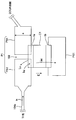
- FIG. 1 is a schematic configuration diagram of an electronic control unit (ECU) according to an embodiment of the present invention.
- FIG. 6 is an explanatory diagram for explaining a noise path in the wiring pattern according to the first embodiment.
- the wiring pattern for connecting the circuit element based on 2nd Embodiment. The example of the circuit element which concerns on 2nd Embodiment.
- the printed circuit board of the present invention applied to an electronic control unit (ECU) mounted on a vehicle will be described.
- ECU electronice control unit
- the printed circuit board of the ECU will be described as an example, but the present invention can be applied to any other printed circuit board.
- FIG. 1 is a schematic configuration diagram of an electronic control unit (ECU) 100 as an example of a printed circuit board to which the present invention is applied.
- the ECU 100 is mounted on the vehicle, and controls the operation of each part of the vehicle, such as engine control, brake control, and airbag control.
- the ECU 100 integrates, for example, a microcomputer 102a that executes various controls based on a program stored in a ROM and data stored in an EEPROM, and a plurality of functions such as a driver circuit and a booster circuit.
- Custom ICs (ASIC) 102b, 102c,... And other circuit components such as diodes, capacitors, resistors, etc. (not shown) are mounted on a printed wiring board (PWB) 101.
- PWB printed wiring board
- the printed wiring board 101 is obtained, for example, by printing a wiring pattern made of a conductive film on the surface of the insulating resin plate 101a and printing a ground surface 107 (FIG. 4) made of a conductive film on the back surface.
- the ECU 100 has external connection terminals T1, T2,... TG for connecting to external devices and circuits.
- the external connection terminals T1 and T2 are signal terminals for transmitting and receiving signals to and from external devices, or power supply terminals for receiving power supply from the outside (or supplying power to the outside).
- the external connection terminal TG is electrically connected to a ground surface 107 provided on the back surface of the printed wiring board 101 through a wiring pattern and a through hole, and the ground surface is electrically grounded to a housing (not shown) of the ECU 100.
- the signal terminals T1, T2 are connected to the circuits (the microcomputer 102a, the ASIC 102b,...) Inside the printed wiring board 101 through the wiring patterns 104 (104a, 104b,).
- the wiring pattern 104a connected to the signal terminal T1 is electrically connected to one terminal of the microcomputer 102a.
- the signal terminal T1 is connected to a microcomputer 102a via, for example, a capacitor C1 for ESD countermeasure, resistors R1 and R2 for voltage conversion, and a filter 103.
- the filter 103 includes, for example, a resistor R3 and a capacitor C2, and removes high frequency noise from the signal.
- FIG. 2 shows a wiring pattern according to the first embodiment of the present invention.
- the capacitor C1 for ESD countermeasure will be described as an example.
- Capacitor C1 is connected to pad P1 and pad PG1.
- the pad P1 includes a first portion PA1 and a second portion PB1 that are electrically insulated from each other.
- the first portion PA1 is connected to the external connection terminal T1 via the wiring pattern 104a, and the first portion PA1 is connected to the external connection terminal T1.
- the second portion PB1 is connected to the wiring pattern 104a on the microcomputer 102a side.
- the pad PG1 is connected to the ground surface 107 on the back surface of the printed wiring board 101 through a through hole.
- the first part PA1 and the second part PB1 of the capacitor C1 are separated from each other by a gap 108 in which a conductive pattern is not formed. That is, for example, a solder resist film is present in the gap 108 region.
- a solder resist film is present in the gap 108 region.
- one electrode 1a of the capacitor C1 is electrically connected to each other across the first portion PA1 and the second portion PB1 of the pad P1. It is adhered by soldering or conductive adhesive.
- the other electrode 1b of the capacitor C1 is bonded to the pad PG1 by soldering or a conductive adhesive.
- the first portion PA1 and the second portion PB1 of the pad P1 are electrically connected by the electrode 1a of the capacitor C1.
- the pads P1 consisting of PB1 configuration that implements the capacitor C1, as shown in FIG. 3, the noise i n by ESD from the outside of the ECU 100, the terminal The first portion PA1 of the pad P1 is reached via T1 and the wiring pattern 104a.
- the noise i n directly from the first portion PA1 can not be propagated to the second portion PB1
- the first portion PA1 is directed to the electrode 1a.
- the impedance change is large at the boundary between the first portion PA1 and the electrode 1a, a part of the noise going from the first portion PA1 to the electrode 1a is reflected (i nr ) and the rest (i ni ). Enters the electrode 1a.
- the noise i ni that has entered the electrode 1a is forced into the capacitor C1, and is emitted from the pad PG1 to the ground plane 107 (FIG. 4) on the back surface through the through hole.
- the noise i n from the outside of the ECU 100 is discharged to the ground plane 107 via the capacitor C1, it is prevented from entering the ECU inside than the first part PA1 of the pad P1.
- the noise generated in the ECU 100 is similarly propagated to the second portion PB1 through the wiring pattern, and then forcibly flows from the electrode 1a into the capacitor C1 and released to the ground plane 107. Therefore, it is possible to prevent noise generated inside the ECU 100 from being released from the terminal T1 to the outside.
- the wiring pattern functions as an antenna, and noise enters from the air via the antenna. There is a risk of affecting ASIC and other circuit components.
- the wiring pattern according to the present embodiment since the wiring pattern is separated into the first portion and the second portion in a state where the capacitor is not connected, the length of the wiring pattern is reduced accordingly. The function as an antenna can be suppressed.
- the wiring pattern may function as a lead wire and propagate flames.
- a capacitor is mounted in the wiring pattern according to this embodiment. The propagation of the flame can be suppressed by the gap 108 of the portion.
- the mounting of the capacitor C1 shown in FIG. 1 is described as an example, but the wiring pattern according to the present embodiment can be similarly applied to the capacitor C2 of the filter 103 as shown in FIG.
- the capacitor C2 is connected to the pad P2 and the pad PG2, and the pad P2 is divided into a first part PA2 and a second part PB2.
- the signal line side pad P2 is separated into the first and second portions PA2 and PB2 is illustrated.
- only the ground line side pad PG2 is connected to the first and second parts PA2 and PB2. You may isolate
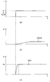
- a minute current i0 (for example, 0.1 ⁇ A: see FIG. 7) is supplied from the microcomputer 102a to the wiring pattern 104a, and the voltage of the wiring pattern 104a is confirmed by an AD converter or the like. Since the capacitance of the filter capacitor C2 is relatively large, such as about several ⁇ F, when the capacitor C2 is normally mounted, the capacitor C2 is not charged by the minute current i0, and the voltage of the wiring pattern 104a hardly increases. . A parasitic capacitance Cp ′ is present between the wiring pattern 104 a and the ground (107, PG 2).
- the parasitic capacitance Cp ′ per 1 cm of the wiring pattern is, for example, about 1 pF.
- the wiring pattern 104a since the wiring pattern 104a extends to the external connection terminal T1 via the pad P2, the parasitic capacitance of the entire wiring pattern 104a becomes a relatively large value and is hardly charged by the minute current i0. Therefore, even when the capacitor C2 is dropped, the parasitic capacitance cannot be charged by the minute current i0, and the voltage of the wiring pattern 104a only rises by about 0.5 mV as shown in FIG. 7B.
- the wiring pattern 104a is separated into the first part PA2 and the second part PB2 at the pad P2, when the capacitor C2 is removed, the wiring pattern 104a is separated from the terminal T11 of the microcomputer 102a. Only the wiring pattern portion 104a ′ up to the second portion PB2 of the pad P2 serves as a load for the minute current i0. In this case, since the length of the wiring pattern portion 104a ′ is short, the parasitic capacitance Cp between the wiring pattern portion 104a ′ and the ground (107, PG2) is also reduced. As shown in FIG.
- the voltage of the wiring pattern portion 104a ′ rises to about 2.5 V in a short time (eg, 300 ⁇ s).
- the capacitor C2 is mounted, the capacitor C2 is not charged by the minute current i0, and the voltage of the wiring pattern portion 104a 'hardly increases. Therefore, it is possible to monitor whether or not the capacitor C2 has dropped off by detecting an increase in the voltage of the wiring pattern portion 104a 'due to the minute current i0. Thereby, it is possible to reduce an additional capacitor compared with the conventional structure.
- FIG. 9 shows two signal wiring patterns L1 and L2 arranged between the reception unit and the modulation unit of the communication circuit, and transmits the same signal to both wiring patterns at the same timing.
- Such signal wiring patterns L1 and L2 are impedance control lines that need to appropriately control the impedance of the signal wiring pattern in order to transmit the same signal at the same timing.
- Such wiring patterns L1 and L2 are used in, for example, a dual mode receiving circuit.
- the pad P3 and the pad P4 are not connected, and when the wiring pattern L1 is used, the pad P3 and the pad P4 are connected by the jumper R4.
- the pad P5 and the pad P6 are not connected, and when the wiring pattern L2 is used, the pad P5 and the pad P6 are connected by the jumper R5.
- the jumpers R4 and R5 are short-circuit elements having a low resistance, for example, a resistance value of several m ⁇ .
- the pad P7 on the wiring pattern L1 side is divided into a first part PA7 and a second part PB7, and the pad P8 on the wiring pattern L2 side is divided.
- the first portion PA8 and the second portion PB8 are divided, and a resistor R6 having a high resistance value is connected between the pad P7 and the pad P8.
- the resistance value of the resistor R6 is set to a high resistance value such that the wiring pattern L1 and the wiring pattern L2 are electrically insulated.
- the resistance value of the resistor R6 depends on the voltage of the signal transmitted through the wiring pattern, but can be about 100 G ⁇ , for example.
- one electrode 6a of the resistor R6 short-circuits the first portion PA7 and the second portion PB7 of the pad P7, and the other electrode 6b of the resistor R6 is connected to the first portion PA8 and the second portion of the pad P8.
- the portion PB8 is short-circuited and the pad P7 and the pad P8 are electrically insulated by a high-resistance resistor R6. That is, the electrode 6a of the resistor R6 functions as a jumper of the wiring pattern L1, and the electrode 6b of the resistor R6 functions as a jumper of the wiring pattern L2.
- both the electrodes 6a and 6b are part of one resistive element R6, the electrodes 6a and 6b have substantially the same characteristics (impedance) without being affected by variations in characteristics between the elements. Therefore, according to the configuration of the present embodiment, the impedances of the wiring pattern L1 and the wiring pattern L2 can be matched with high accuracy.
- the short circuit in each of the two wiring patterns can be performed by one resistance element R6, the short circuit is compared with the case where a jumper is provided for each wiring pattern. It is possible to reduce the number of elements used for.
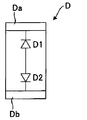
- the Zener diode includes two diodes D1 and D2, and uses a package component in which the anodes of the diodes are connected to each other and the cathodes of the diodes are connected to the electrodes Da and Db, respectively. Is possible.
- the impedance control line arranged between the reception unit and the modulation unit of the communication circuit has been described.
- an arbitrary wiring pattern that transmits the same signal to a plurality of wiring patterns at the same timing It is applicable to.
- the present invention can also be applied to a case where a clock signal is input from a crystal oscillator to a microcomputer via a plurality of wiring patterns.
- C1 to C2 Capacitors 1a, 1b, 2a, 2b, 6a, 6b: Electrode 2, P1 to P8, PG1 to PG2: Pad 3 Wiring pattern 4 Branch pattern 5, R1 to R3, R6 Resistance 100 ECU (printed circuit Board) 101 Printed wiring board 102a Microcomputer 102b, 102c ASIC T1, T2, TG Signal terminal or power supply terminal 107 Ground plane
Landscapes
- Structure Of Printed Boards (AREA)
- Printing Elements For Providing Electric Connections Between Printed Circuits (AREA)
Abstract
回路部品をノイズやサージから効果的に保護することが可能なプリント回路板を提供することを目的とする。 第1の配線パターン(104a;L1)及び第2の配線パターン(PG1;PG2;L2)を備え、前記第1の配線パターンが電気的に互いに絶縁された第1の部分(PA1;PA2;PA3)と第2の部分(PB1;PB2;PB3)とに分割されたプリント配線板(101)と;第1の電極(1a;2a;6a)及び第2の電極(1b;2b;6b)を有する回路素子(C1;C2;R6)であって、前記第1の電極が、前記第1の配線パターンの前記第1の部分と前記第2の部分とを電気的に接続するように配置されるとともに、前記第2の電極が、前記第2の配線パターンに接続される前記回路素子と;を備えるプリント回路板。
Description
本発明は、実装される電気部品及び電気回路をノイズから保護するための配線パターンを備えたプリント回路板に関する。
車両に搭載される電子制御ユニット(ECU)は、ドライバ回路や昇圧回路などの複数の機能を集積したカスタムIC(ASIC)と、マイクロコンピュータ(マイコン)と、ダイオード、キャパシタ、抵抗等の他の回路部品とがプリント配線板(PWB)上に実装されて構成される。これらの回路部品は、プリント配線板の一表面に配置され、半田付け又は接着される。この実装方法は、面実装(SMT:Surface Mount Technology)と呼ばれ、面実装用の部品は、面実装部品(SMD:Surface Mount Device)と呼ばれる。各回路部品は、回路の機能を確実にする目的や、外部からの電磁妨害雑音(EMI)や静電気放電パルス(ESDサージ)等のノイズがECU内部に侵入しないように遮断したり、ECU内部で発生するノイズが外部回路に伝搬しないように遮断する目的など異なる目的を有する。
ノイズ対策用の回路部品の例としては、ECUの端子に接続するキャパシタが挙げられる。このキャパシタにより、外部からECUの端子に入るノイズを吸収させてECU内部の回路への影響を防止するとともに、ECU内部で発生したノイズを吸収させてEUC外部の回路への影響を防止する。
しかし、実際には、キャパシタと配線パターンとの接触部分にインダクタンス成分を有し、このインダクタンス成分は高周波信号に対して大きくなる。例えば、図10Aに示すように分岐パターン4を用いてキャパシタ1を接続する場合には、分岐パターン4のインダクタンス成分及び分岐パターン4とキャパシタ1の電極1aとの間の接触部分のインダクタンス成分が高周波信号に対して大きくなり、高周波のノイズパルスが、キャパシタ1に十分吸収されず、低抵抗の部分、例えば、マイクロコンピュータやASICの入力部に侵入し、これらを破壊するおそれがある。このようなインダクタンス成分を低減するために、キャパシタ1をいわゆる釘の目技術(EYE OF NEEDLE TECHNIQUE)を用いて配線パターンに接続する方法がある。この接続方法は、図10Bに示すように、面実装用キャパシタC1の一方の電極1aを信号ライン(又は電源ライン)3に直接半田付け等で接続し、他方の電極1bをグランド電位に繋がるパッド2に接続するものである。この接続方法によれば、図10Aに示すように、信号ライン3からの分岐パターン4を介してキャパシタC1の一方の電極1aを信号ライン3に接続する場合に比較して、分岐パターン4の分のインダクタンス成分を低減することができる。しかしながら、この釘の目技術による接続方法でも、キャパシタと配線パターンとの接触部分のインダクタンス成分を低減することはできず、ノイズパルスがキャパシタC1に吸収されずに信号パターン3を介して伝搬するおそれがある。
回路保護用のキャパシタのインダクタンス成分を低減する方法として、従来、例えば特許文献1に記載された保護回路がある。この保護回路は、画像処理用LSIのように、デジタル処理部とアナログ処理部とが同一基板上に混載されたLSI(デジアナ混載LSI)において、バイパスキャパシタ60の上部電極(第2配線層)28を電源ライン40と共用し、下部電極(第1配線層)26を、複数のプラグ25、P型拡散層21及び半導体基板20を介してグランド電位(第1配線層26)にバイアスしている。バイパスキャパシタ60の下部電極26が複数のプラグ25を介して半導体基板20に接続されるため、半導体基板20とバイパスキャパシタ60との間の電流は複数のプラグ25に分散され、各プラグ25の電流密度が小さく抑えられる。また、半導体基板20は、その裏面からグランド電位にバイアスされているため、バイパスキャパシタ60を充放電するための電流経路は、半導体基板20の厚さ方向に形成され、電流は半導体基板20の内部で分散され、半導体基板20自体の残留インダクタンスが小さくなる。これにより、バイパスキャパシタ60の下部電極26に付随する残留インダクタンスを小さくしている。更に、このLSIでは、半導体基板20上において、アナログ回路部30とデジタル回路部40との間にガードリング50を形成して、デジタル回路部40で発生したノイズがアナログ回路部30に伝搬することを防止している。
しかしながら、プリント配線板に実装されるキャパシタのインダクタンス成分の低減においては、特許文献1に記載されたように、キャパシタの電極を電源ラインと共用することはできず、また、半導体基板を介してキャパシタをグランドにバイアスする方法やガードリングによりノイズの伝搬を遮断する方法を採用することはできない。
本発明は、回路部品をノイズから効果的に保護することが可能なプリント配線板を提供することを目的とする。
本発明に係るプリント回路板(100)であって、第1の配線パターン(104a;L1)及び第2の配線パターン(PG1;PG2;L2)を備え、前記第1の配線パターンが電気的に互いに絶縁された第1の部分(PA1;PA2;PA3)と第2の部分(PB1;PB2;PB3)とに分割されたプリント配線板(101)と;第1の電極(1a;2a;6a)及び第2の電極(1b;2b;6b)を有する回路素子(C1;C2;R6)であって、前記第1の電極が、前記第1の配線パターンの前記第1の部分と前記第2の部分とを電気的に接続するように配置されるとともに、前記第2の電極が、前記第2の配線パターンに接続される前記回路素子と;を備える。
本発明の一実施形態では、前記第1の配線パターンに微小電流を供給した場合における、該第1の配線パターンの電圧を検出することにより、前記回路素子の脱落の有無を検出するように構成されている。
本発明の一実施形態では、更に、第2の配線パターンが電気的に互いに絶縁された第3の部分と第4の部分とに分割されており、前記回路素子の第2の電極は、前記第2の配線パターンの第3の部分と第4の部分とを電気的に接続するように配置される。
本発明の一実施形態では、前記回路素子の第1の電極が第1の配線パターンにおけるジャンパとして機能し、前記回路素子の第2の電極が第2の配線パターンにおけるジャンパとして機能する。本発明の一実施形態では、前記回路素子は、抵抗、キャパシタ、バリスタ又はツェナーダイオードの何れかである。
本発明に係るプリント配線板(101)は、回路素子(C1;C2;R6)の第1の電極(1a;2a;6a)及び第2の電極(1b;2b;6b)をそれぞれ接続するための第1の配線パターン(104a;L1)及び第2の配線パターン(PG1;PG2;L2)を備え、前記第1の配線パターンが電気的に互いに絶縁された第1の部分(PA1;PA2;PA3)と第2の部分(PB1;PB2;PB3)とに分割されており、前記第1の部分と前記第2の部分の間隔は、前記回路素子の第1の電極が前記第1の部分と前記第2の部分とを電気的に接続するように配置可能に設定されている。
以下、車両に搭載される電子制御ユニット(ECU)に適用される本発明のプリント回路板について説明する。なお、ここでは、ECUのプリント回路板を例に挙げて説明するが、本発明は他の任意のプリント回路板に適用可能である。
(第1実施形態)
図1は、本発明が適用されるプリント回路板の一例としての電子制御ユニット(ECU)100の概略構成図である。ECU100は、車両に搭載され、エンジン制御、ブレーキ制御、エアバッグ制御等、車両各部の動作の制御を実行する。
図1は、本発明が適用されるプリント回路板の一例としての電子制御ユニット(ECU)100の概略構成図である。ECU100は、車両に搭載され、エンジン制御、ブレーキ制御、エアバッグ制御等、車両各部の動作の制御を実行する。
ECU100は、図1に示すように、例えば、ROMに記憶されたプログラムやEEPROMに記憶されたデータに基づいて各種制御を実行するマイコン102aと、ドライバ回路や昇圧回路などの複数の機能を集積したカスタムIC(ASIC)102b、102c・・・と、図示しないダイオード、キャパシタ、抵抗等の他の回路部品とがプリント配線板(PWB)101上に実装されて構成される。
プリント配線板101は、例えば、絶縁樹脂板101aの表面に導電膜からなる配線パターンを印刷し、裏面に導電膜からなるグランド面107(図4)を印刷したものである。ECU100は、外部の機器及び回路と接続するための外部接続端子T1、T2、・・・、TGを有している。外部接続端子T1、T2は、外部の機器との間で信号を送受信するための信号端子、又は、外部から電源の供給を受ける(又は外部に電源を供給する)ための電源端子である。外部接続端子TGは、プリント配線板101の裏面に設けられたグランド面107に配線パターン及びスルーホールを介して導通されており、グランド面はECU100のハウジング(図示せず)に電気的に接地されている。信号端子T1、T2は、配線パターン104(104a、104b、・・・)を介して、プリント配線板101内部の回路(マイコン102a、ASIC102b・・・)に接続されている。例えば、この例では、信号端子T1に接続される配線パターン104aは、マイコン102aの一の端子に電気的に接続される。
信号端子T1は、例えば、ESD対策用のキャパシタC1、電圧変換用の抵抗R1、R2、フィルタ103を介してマイクロコンピュータ(マイコン)102aに接続される。フィルタ103は、例えば、抵抗R3及びキャパシタC2からなり、信号から高周波ノイズを除去する。
図2は、本発明の第1の実施形態に係る配線パターンを示す。ここでは、ESD対策用のキャパシタC1を例に挙げて説明する。キャパシタC1は、パッドP1とパッドPG1とに接続される。ここでは、パッドP1は、電気的に互いに絶縁された第1の部分PA1と第2の部分PB1とからなり、第1の部分PA1が配線パターン104aを介して外部接続端子T1に接続され、第2の部分PB1がマイコン102a側の配線パターン104aに接続されている。パッドPG1は、スルーホールを介してプリント配線板101の裏面のグランド面107に接続されている。
キャパシタC1の第1の部分PA1と第2の部分PB1とは、導電パターンが形成されないギャップ108によって互いに分離されている。つまり、ギャップ108の領域には、例えば、ソルダーレジスト膜が存在する。パッドP1、PG1の間にキャパシタC1を配置する際には、キャパシタC1の一方の電極1aが、パッドP1の第1の部分PA1と第2の部分PB1とを跨いで両者を互いに電気的に接続するように半田付け又は導電性接着剤により接着される。キャパシタC1の他方の電極1bは、パッドPG1に半田付け又は導電性接着剤により接着される。キャパシタC1が実装された状態では、パッドP1の第1の部分PA1及び第2の部分PB1がキャパシタC1の電極1aにより電気的に接続される。
以上のように、電気的に絶縁された2つの部分PA1、PB1からなるパッドP1にキャパシタC1を実装した構成では、図3に示すように、ECU100の外部からのESDによるノイズinは、端子T1、配線パターン104aを経由して、パッドP1の第1の部分PA1に至る。ここで、第1の部分PA1と第2の部分PB1とがギャップ108によって分離されているため、ノイズinは、第1の部分PA1から直接、第2の部分PB1に伝搬することはできず、第1の部分PA1から電極1aに向かうことになる。また、第1の部分PA1と電極1aとの境界ではインピーダンス変化が大きいので、第1の部分PA1から電極1aに向かおうとするノイズの一部は反射され(inr)、残り(ini)が電極1aに入る。電極1aに入ったノイズiniは、強制的にキャパシタC1内部に流し込まれ、パッドPG1からスルーホールを介して裏面のグランド面107(図4)に放出される。この結果、ECU100の外部からのノイズinは、キャパシタC1を介してグランド面107に放出され、パッドP1の第1の部分PA1よりもECU内側に侵入することが防止される。
第1の部分PA1から電極1aに流れ込んだノイズiniが、キャパシタC1内部に強制的に流される理由を説明する。第1に、図4に示すように、第1の部分PA1のギャップ108側の部分では、第1の部分PA1から裏面のグランド面107に向かう電界Eが形成される。また、図3に示すように、スルーホールを介してグランド面107に接続されているパッドPG1と第1の部分PA1との間にも、第1の部分PA1からパッドPG1に向かう電界Eが形成される。これらの電界は、電極1aに流れ込んだノイズiniをキャパシタC1の内部に強制的に流すように作用する。第2に、電極1aとパッドP1の第2の部分PB1との間にも、大きなインピーダンス変化があるので、電極1aに流れ込んだノイズは、第2の部分PB1に向かって流れ難く、キャパシタC1の内部に向かって流れやすい。この結果、第1の部分PA1から電極1aに流れ込んだノイズiniが、キャパシタC1内部に強制的に流される。
なお、ECU100の内部で発生するノイズについても同様に、配線パターンを介して第2の部分PB1に伝搬された後、電極1aからキャパシタC1内部に強制的に流されてグランド面107に放出されるため、ECU100の内部で発生するノイズが端子T1から外部に放出されるのを防止することができる。
図3では、信号ライン側のパッドP1を第1及び第2の部分PA1、PB1に分離する例を説明したが、グランドライン側のパッドPG1も同様に第1及び第2の部分に分離しても良い。この場合、信号ラインからのノイズの侵入を防止し、信号ラインを介して外部にノイズが漏出することを防止できるとともに、グランドラインからのノイズの侵入を防止し、グランドラインを介して外部にノイズが漏出することを防止することができる。
また、グランドライン側のパッドPG1のみを第1及び第2の部分に分離し、グランドラインからのノイズの侵入を防止するとともに、グランドラインを介して外部にノイズが漏出することを防止しても良い。
プリント配線板101では、回路が使用されておらず、キャパシタ及び他の回路部品が実装されていない場合には、配線パターンはアンテナとして機能し、空中からアンテナを介してノイズが侵入し、マイコン、ASIC、他の回路部品に影響を及ぼすおそれがある。本実施形態に係る配線パターンによれば、キャパシタが接続されていない状態では配線パターンが第1の部分と第2の部分とに分離されるため、その分、配線パターンの長さが短くなり、アンテナとしての機能を抑制することができる。
また、何らかの原因(熱腐食など)によりECU100内部の回路が発火した場合には、配線パターンが導火線のように機能して炎を伝搬するおそれがあるが、本実施形態に係る配線パターンではキャパシタ実装部分のギャップ108により、炎の伝搬を抑制することができる。
上記では、図1示すキャパシタC1の実装を例に挙げて説明したが、フィルタ103のキャパシタC2についても、図5に示すように、本実施形態に係る配線パターンを同様に適用できる。図5に示すように、キャパシタC2は、パッドP2とパッドPG2とに接続され、パッドP2が第1の部分PA2と第2の部分PB2とに分割されている。ここでは、信号ライン側のパッドP2を第1及び第2の部分PA2、PB2に分離する例を図示しているが、キャパシタC1の場合と同様に、グランドライン側のパッドPG2のみを第1及び第2の部分に分離しても良く、パッドP2及びPG2の両方を第1及び第2の部分に分離しても良い。
また、図5に示す2つに分離されたパッドP2を用いる場合には、キャパシタC2の脱落の検知が可能になる。以下、キャパシタC2の脱落の検知について説明する。
先ず、フィルタ用のキャパシタの従来技術に係る実装構造を、図6を参照して説明する。この構成において、マイコン102aから微小電流i0(例えば、0.1μA:図7参照)を配線パターン104aに供給し、ADコンバータ等で配線パターン104aの電圧を確認する。フィルタ用のキャパシタC2の静電容量は数μF程度と比較的大きいので、キャパシタC2が正常に実装されている場合、キャパシタC2は微小電流i0によって充電されず、配線パターン104aの電圧は殆ど上昇しない。また、配線パターン104aとグランド(107、PG2)との間には、寄生容量Cp’が存在する。配線パターン1cm当たりの寄生容量Cp’は例えば、1pF程度である。しかし、図6の構造では、配線パターン104aはパッドP2を介して、外部接続端子T1まで延びているので、配線パターン104a全体の寄生容量は比較的大きな値となり、微小電流i0によってほとんど充電されない。従って、キャパシタC2が脱落した場合にも、微小電流i0によって寄生容量を充電することができず、図7(b)に示すように、配線パターン104aの電圧は0.5mV程度しか上昇しない。この結果、図6の構成では、微小電流i0を配線パターン104aに供給することによりキャパシタC2の脱落の有無を検出することはできない。このため、従来、1個のキャパシタが脱落した場合にもフィルタの機能を維持できるように、キャパシタを並列に2個配置する必要があった。
一方、図5に示す本発明の構成では、配線パターン104aがパッドP2において第1の部分PA2と第2の部分PB2とに分離されているため、キャパシタC2の脱落時には、マイコン102aの端子T11からパッドP2の第2の部分PB2までの配線パターン部分104a’だけが、微小電流i0に対する負荷となる。この場合、配線パターン部分104a’の長さが短いので、配線パターン部分104a’とグランド(107、PG2)との間の寄生容量Cpも小さくなり、図7(c)に示すように、微小電流i0により配線パターン部分104a’の電圧が短時間(例えば300μs)の間に2.5V程度まで上昇する。一方、キャパシタC2が実装されている場合には、微小電流i0によりキャパシタC2が充電されず、配線パターン部分104a’の電圧はほとんど上昇しない。よって、微小電流i0による配線パターン部分104a’の電圧の上昇を検出することにより、キャパシタC2の脱落の有無を監視することが可能である。これにより、従来の構成と比較して、追加のキャパシタを削減することが可能である。
[第2実施形態]
図9は、通信回路の受信部と変調部との間に配置される2つの信号配線パターンL1、L2であって、両配線パターンに同一信号を同一タイミングで伝送する配線パターンを示す。このような信号配線パターンL1、L2は、同一信号を同一タイミングで伝送するために信号配線パターンのインピーダンスを適切に制御する必要があるインピーダンス制御ラインである。
図9は、通信回路の受信部と変調部との間に配置される2つの信号配線パターンL1、L2であって、両配線パターンに同一信号を同一タイミングで伝送する配線パターンを示す。このような信号配線パターンL1、L2は、同一信号を同一タイミングで伝送するために信号配線パターンのインピーダンスを適切に制御する必要があるインピーダンス制御ラインである。
このような配線パターンL1、L2は、例えば、デュアルモードの受信回路等に使用される。配線パターンL1を使用しない場合にはパッドP3とパッドP4を未接続とし、配線パターンL1を使用する場合に、ジャンパR4によりパッドP3とパッドP4を接続する。配線パターンL2を使用しない場合にはパッドP5とパッドP6を未接続とし、配線パターンL2を使用する場合に、ジャンパR5によりパッドP5とパッドP6を接続する。ジャンパR4、R5は、低抵抗、例えば、数mΩの抵抗値を有する短絡用の素子である。
図9の従来の構成では、各配線パターンL1、L2のそれぞれにおいて、別々のジャンパR4、R5を使用するため、個々のジャンパの製造公差により、ジャンパR4、R5のインピーダンス等の特性にばらつきを生じる。このような特性のばらつきは、各配線パターンL1、L2を介して受け取る信号のタイミングのずれ(位相のずれ)を引き起こす。特に、例えば1GHz以上の高周波の信号を各配線パターンL1、L2を介して伝送する場合には、タイミングのずれにより、信号の処理に支障をきたす可能性が大きくなる問題がある。
これに対して、本実施形態では、図8Aに示すように、配線パターンL1側のパッドP7を第1の部分PA7と第2の部分PB7とに分割するとともに、配線パターンL2側のパッドP8を第1の部分PA8と第2の部分PB8とに分割し、パッドP7とパッドP8の間に高抵抗値を有する抵抗R6を接続する。抵抗R6の抵抗値は、配線パターンL1と配線パターンL2との間が電気的に絶縁される程度の高抵抗値とする。抵抗R6の抵抗値は、配線パターンを伝送する信号の電圧に依存するが、例えば、100GΩ程度とすることができる。
この構成では、抵抗R6の一方の電極6aがパッドP7の第1の部分PA7と第2の部分PB7とを短絡し、抵抗R6の他方の電極6bがパッドP8の第1の部分PA8と第2の部分PB8とを短絡するとともに、パッドP7とパッドP8との間は高抵抗値の抵抗R6によって電気的に絶縁される。つまり、抵抗R6の電極6aが配線パターンL1のジャンパとして機能し、抵抗R6の電極6bが配線パターンL2のジャンパとして機能する。電極6a及び6bは共に1つの抵抗素子R6の一部であるため、素子間の特性のばらつきに影響されず、電極6aと電極6bとは略同一の特性(インピーダンス)を有する。従って、本実施形態の構成によれば、配線パターンL1及び配線パターンL2の各インピーダンスを高精度に整合させることができる。
また、図8Aの本実施形態の構成によれば、2本の配線パターン各々における短絡を1つの抵抗素子R6で行うことができるので、各配線パターンごとにジャンパを設ける場合に比較して、短絡に用いる素子の数を低減することができる。
なお、上記では、各々2つに分割されたパッド間に抵抗を配置する場合を説明したが、抵抗に代えて、キャパシタ、バリスタ、ツェナーダイオード等を配置するようにしても良い。ツェナーダイオードは、例えば、図8Bに示すように、2つのダイオードD1,D2を含み、各ダイオードのアノード同士が接続され、各ダイオードのカソードが電極Da、Dbにそれぞれ接続されたパッケージ部品を用いることが可能である。
なお、上記では、通信回路の受信部と変調部との間に配置されるインピーダンス制御ラインについて説明したが、本実施形態は、複数の配線パターンに同一信号を同一タイミングで伝送する任意の配線パターンに適用可能である。例えば、水晶発振器から複数の配線パターンを介してマイコンにクロック信号を入力する場合にも適用可能である。
1、C1~C2:キャパシタ
1a、1b、2a、2b、6a、6b:電極
2、P1~P8、PG1~PG2:パッド
3 配線パターン
4 分岐パターン
5、R1~R3、R6 抵抗
100 ECU(プリント回路板)
101 プリント配線板
102a マイコン
102b、102c ASIC
T1、T2、TG 信号端子又は電源端子
107 グランド面
1a、1b、2a、2b、6a、6b:電極
2、P1~P8、PG1~PG2:パッド
3 配線パターン
4 分岐パターン
5、R1~R3、R6 抵抗
100 ECU(プリント回路板)
101 プリント配線板
102a マイコン
102b、102c ASIC
T1、T2、TG 信号端子又は電源端子
107 グランド面
Claims (5)
- プリント回路板(100)であって、
第1の配線パターン(104a;L1)及び第2の配線パターン(PG1;PG2;L2)を備え、前記第1の配線パターンが電気的に互いに絶縁された第1の部分(PA1;PA2;PA3)と第2の部分(PB1;PB2;PB3)とに分割されたプリント配線板(101)と、
第1の電極(1a;2a;6a)及び第2の電極(1b;2b;6b)を有する回路素子(C1;C2;R6)であって、前記第1の電極が、前記第1の配線パターンの前記第1の部分と前記第2の部分とを電気的に接続するように配置されるとともに、前記第2の電極が、前記第2の配線パターンに接続される前記回路素子と、
を備えるプリント回路板。 - 請求項1に記載のプリント回路板において、
前記第1の配線パターンに微小電流を供給した場合における、該第1の配線パターンの電圧を検出することにより、前記回路素子の脱落の有無を検出するように構成されている、プリント回路板。 - 請求項1又は2に記載のプリント回路板において、
更に、第2の配線パターンが電気的に互いに絶縁された第3の部分と第4の部分とに分割されており、
前記回路素子の第2の電極は、前記第2の配線パターンの第3の部分と第4の部分とを電気的に接続するように配置される、プリント回路板。 - 請求項3に記載のプリント回路板において、前記回路素子の第1の電極が第1の配線パターンにおけるジャンパとして機能し、前記回路素子の第2の電極が第2の配線パターンにおけるジャンパとして機能する、プリント回路板。
- 請求項4に記載のプリント回路板において、前記回路素子は、抵抗、キャパシタ、バリスタ又はツェナーダイオードの何れかである、プリント回路板。
Priority Applications (1)
| Application Number | Priority Date | Filing Date | Title |
|---|---|---|---|
| JP2012521354A JPWO2011162005A1 (ja) | 2010-06-24 | 2011-04-01 | プリント回路板 |
Applications Claiming Priority (2)
| Application Number | Priority Date | Filing Date | Title |
|---|---|---|---|
| JP2010143898 | 2010-06-24 | ||
| JP2010-143898 | 2010-06-24 |
Publications (1)
| Publication Number | Publication Date |
|---|---|
| WO2011162005A1 true WO2011162005A1 (ja) | 2011-12-29 |
Family
ID=45371209
Family Applications (1)
| Application Number | Title | Priority Date | Filing Date |
|---|---|---|---|
| PCT/JP2011/058383 Ceased WO2011162005A1 (ja) | 2010-06-24 | 2011-04-01 | プリント回路板 |
Country Status (2)
| Country | Link |
|---|---|
| JP (1) | JPWO2011162005A1 (ja) |
| WO (1) | WO2011162005A1 (ja) |
Cited By (3)
| Publication number | Priority date | Publication date | Assignee | Title |
|---|---|---|---|---|
| JP2013220676A (ja) * | 2012-04-13 | 2013-10-28 | Yazaki Corp | ジャンクションボックス |
| KR20150034318A (ko) * | 2013-09-26 | 2015-04-03 | 삼성디스플레이 주식회사 | Dc-dc 컨버터 및 이를 포함하는 표시 장치 |
| JP2017083267A (ja) * | 2015-10-27 | 2017-05-18 | Tdk株式会社 | 電子回路及び電子機器 |
Citations (3)
| Publication number | Priority date | Publication date | Assignee | Title |
|---|---|---|---|---|
| JPS6292457A (ja) * | 1985-10-18 | 1987-04-27 | Fuji Xerox Co Ltd | 厚膜抵抗回路の形成方法 |
| JP2000150796A (ja) * | 1998-11-13 | 2000-05-30 | Nec Corp | 半導体装置 |
| WO2006112501A1 (ja) * | 2005-04-20 | 2006-10-26 | Matsushita Electric Industrial Co., Ltd. | 二次電池の保護回路、電池パック、及び感熱保護スイッチ装置 |
Family Cites Families (7)
| Publication number | Priority date | Publication date | Assignee | Title |
|---|---|---|---|---|
| JPH02237091A (ja) * | 1989-03-09 | 1990-09-19 | Fujitsu Ltd | 印刷配線板 |
| GB2272108B (en) * | 1992-11-03 | 1995-10-18 | Smiths Industries Plc | Electrical assemblies |
| JPH07183627A (ja) * | 1993-12-22 | 1995-07-21 | Rohm Co Ltd | 部品実装プリント基板 |
| JP2882994B2 (ja) * | 1994-03-11 | 1999-04-19 | 株式会社ピーエフユー | コンデンサを実装したプリント板 |
| JPH10145015A (ja) * | 1996-11-11 | 1998-05-29 | Sumitomo Wiring Syst Ltd | プリント配線板の回路パターン |
| IES81163B2 (en) * | 1998-07-15 | 2000-05-17 | Artesyn Tech | A conductor |
| JP2010021209A (ja) * | 2008-07-08 | 2010-01-28 | Mitsumi Electric Co Ltd | 放電ギャップパターン及び電源装置 |
-
2011
- 2011-04-01 WO PCT/JP2011/058383 patent/WO2011162005A1/ja not_active Ceased
- 2011-04-01 JP JP2012521354A patent/JPWO2011162005A1/ja active Pending
Patent Citations (3)
| Publication number | Priority date | Publication date | Assignee | Title |
|---|---|---|---|---|
| JPS6292457A (ja) * | 1985-10-18 | 1987-04-27 | Fuji Xerox Co Ltd | 厚膜抵抗回路の形成方法 |
| JP2000150796A (ja) * | 1998-11-13 | 2000-05-30 | Nec Corp | 半導体装置 |
| WO2006112501A1 (ja) * | 2005-04-20 | 2006-10-26 | Matsushita Electric Industrial Co., Ltd. | 二次電池の保護回路、電池パック、及び感熱保護スイッチ装置 |
Cited By (4)
| Publication number | Priority date | Publication date | Assignee | Title |
|---|---|---|---|---|
| JP2013220676A (ja) * | 2012-04-13 | 2013-10-28 | Yazaki Corp | ジャンクションボックス |
| KR20150034318A (ko) * | 2013-09-26 | 2015-04-03 | 삼성디스플레이 주식회사 | Dc-dc 컨버터 및 이를 포함하는 표시 장치 |
| KR102277986B1 (ko) * | 2013-09-26 | 2021-07-16 | 삼성디스플레이 주식회사 | Dc-dc 컨버터 및 이를 포함하는 표시 장치 |
| JP2017083267A (ja) * | 2015-10-27 | 2017-05-18 | Tdk株式会社 | 電子回路及び電子機器 |
Also Published As
| Publication number | Publication date |
|---|---|
| JPWO2011162005A1 (ja) | 2013-08-19 |
Similar Documents
| Publication | Publication Date | Title |
|---|---|---|
| CN101689750B (zh) | 火花间隙装置、无线装置及静电放电保护方法 | |
| US9345140B2 (en) | Printed circuit board | |
| US20020151200A1 (en) | Device for protecting an electric and/or electronic component arranged on a carrier substrate against electrostatic discharges | |
| US8582273B2 (en) | Surge absorbing circuit and electric device using the same | |
| US6185105B1 (en) | Discharge structure of printed circuit board | |
| CN117095616A (zh) | 显示模组和显示装置 | |
| WO2011162005A1 (ja) | プリント回路板 | |
| US7495880B2 (en) | Circuit board and electric device having circuit board | |
| KR20170124270A (ko) | 인쇄회로기판 및 이를 포함하는 전자부품패키지 | |
| JP2003151794A (ja) | 自動車用電子制御装置 | |
| JP2013148753A (ja) | 車両用表示装置の回路基板 | |
| US8441805B2 (en) | Circuit board mounting structure of compound circuit | |
| JP6373912B2 (ja) | ノイズフィルタ、及び当該ノイズフィルタが形成された回路基板 | |
| JP4996193B2 (ja) | 配線基板、半導体パッケージ | |
| US8258407B2 (en) | Wiring board and method of preventing high voltage damage | |
| JPH1126907A (ja) | プリント配線板および電子機器 | |
| KR101109688B1 (ko) | 정전기 방지용 커패시터가 접합된 발광 다이오드 | |
| JP4893114B2 (ja) | 多層配線基板 | |
| CN218976906U (zh) | Pcb、pcba及tof深度相机 | |
| JP2009283519A (ja) | プリント配線板の接続構造 | |
| JP2004023074A (ja) | 回路基板装置及びその製造方法 | |
| CN117042285A (zh) | Pcb板的静电保护电路及其设计方法 | |
| KR20250014189A (ko) | 티코일 패터닝이 적용되는 반도체 칩 패키지 | |
| JPH0832200A (ja) | 電気回路板及びプリント配線板 | |
| JPH1079563A (ja) | 電子回路基板およびその製造方法、それを備えた光電スイッチならびにそれを備えた近接スイッチ |
Legal Events
| Date | Code | Title | Description |
|---|---|---|---|
| 121 | Ep: the epo has been informed by wipo that ep was designated in this application |
Ref document number: 11797893 Country of ref document: EP Kind code of ref document: A1 |
|
| WWE | Wipo information: entry into national phase |
Ref document number: 2012521354 Country of ref document: JP |
|
| NENP | Non-entry into the national phase |
Ref country code: DE |
|
| 122 | Ep: pct application non-entry in european phase |
Ref document number: 11797893 Country of ref document: EP Kind code of ref document: A1 |