WO2011129283A1 - 隔壁の修正方法 - Google Patents
隔壁の修正方法 Download PDFInfo
- Publication number
- WO2011129283A1 WO2011129283A1 PCT/JP2011/058935 JP2011058935W WO2011129283A1 WO 2011129283 A1 WO2011129283 A1 WO 2011129283A1 JP 2011058935 W JP2011058935 W JP 2011058935W WO 2011129283 A1 WO2011129283 A1 WO 2011129283A1
- Authority
- WO
- WIPO (PCT)
- Prior art keywords
- correction
- ink
- partition
- partition wall
- curable
- Prior art date
- Legal status (The legal status is an assumption and is not a legal conclusion. Google has not performed a legal analysis and makes no representation as to the accuracy of the status listed.)
- Ceased
Links
Images

Classifications
-
- H—ELECTRICITY
- H10—SEMICONDUCTOR DEVICES; ELECTRIC SOLID-STATE DEVICES NOT OTHERWISE PROVIDED FOR
- H10K—ORGANIC ELECTRIC SOLID-STATE DEVICES
- H10K59/00—Integrated devices, or assemblies of multiple devices, comprising at least one organic light-emitting element covered by group H10K50/00
- H10K59/10—OLED displays
- H10K59/12—Active-matrix OLED [AMOLED] displays
- H10K59/122—Pixel-defining structures or layers, e.g. banks
-
- G—PHYSICS
- G02—OPTICS
- G02B—OPTICAL ELEMENTS, SYSTEMS OR APPARATUS
- G02B5/00—Optical elements other than lenses
- G02B5/20—Filters
- G02B5/201—Filters in the form of arrays
-
- G—PHYSICS
- G02—OPTICS
- G02B—OPTICAL ELEMENTS, SYSTEMS OR APPARATUS
- G02B5/00—Optical elements other than lenses
- G02B5/20—Filters
- G02B5/22—Absorbing filters
- G02B5/223—Absorbing filters containing organic substances, e.g. dyes, inks or pigments
-
- H—ELECTRICITY
- H10—SEMICONDUCTOR DEVICES; ELECTRIC SOLID-STATE DEVICES NOT OTHERWISE PROVIDED FOR
- H10K—ORGANIC ELECTRIC SOLID-STATE DEVICES
- H10K59/00—Integrated devices, or assemblies of multiple devices, comprising at least one organic light-emitting element covered by group H10K50/00
- H10K59/10—OLED displays
- H10K59/17—Passive-matrix OLED displays
- H10K59/173—Passive-matrix OLED displays comprising banks or shadow masks
-
- H—ELECTRICITY
- H10—SEMICONDUCTOR DEVICES; ELECTRIC SOLID-STATE DEVICES NOT OTHERWISE PROVIDED FOR
- H10K—ORGANIC ELECTRIC SOLID-STATE DEVICES
- H10K71/00—Manufacture or treatment specially adapted for the organic devices covered by this subclass
- H10K71/861—Repairing
-
- H—ELECTRICITY
- H10—SEMICONDUCTOR DEVICES; ELECTRIC SOLID-STATE DEVICES NOT OTHERWISE PROVIDED FOR
- H10K—ORGANIC ELECTRIC SOLID-STATE DEVICES
- H10K2102/00—Constructional details relating to the organic devices covered by this subclass
- H10K2102/301—Details of OLEDs
- H10K2102/351—Thickness
Definitions
- the present invention relates to a method for correcting a chip defect of a partition wall that divides a surface of a substrate into a plurality of sections.
- a cost reduction process using an inkjet method has been proposed as a method of manufacturing a color filter or an organic EL (Electro-Luminescence) element.
- a color filter or an organic EL (Electro-Luminescence) element For example, in the manufacture of a color filter, after forming partition walls having liquid repellency, R (red), G (green), and B (blue) inks are applied to the pixel regions defined by the partition walls by an inkjet method. A pixel having a colored layer is formed.
- an ink which is a solution of a hole transport material and a light-emitting material is applied to a pixel region partitioned by the partition wall by an inkjet method, A pixel having a hole transport layer, a light emitting layer, and the like is formed.
- Patent Document 1 discloses an ink repellency after forming an undercoat layer at a correction portion for a defect in a partition wall. A technique for correcting with a repair ink containing an agent has been proposed.
- Patent Document 1 since the repair ink containing the ink repellent material is thermally cured and no special treatment is performed, the entire surface of the formed film becomes ink repellent. Therefore, after the barrier rib correction, the wettability of the ink in the portion corresponding to the side surface of the barrier rib is reduced in the corrected portion, and the thickness of the formed colored layer (pixel) is closer to the side surface of the barrier rib correction portion than the pixel center portion. There is a problem that the thinning occurs and so-called white spots occur.
- the present invention has been made to solve the above-described problems of the prior art, and has an ink repellency on the upper surface formed on the substrate in order to form a plurality of sections on the substrate.
- the chip defect generated in the partition wall having ink affinity on the side surface is corrected so as to have ink repellency only on the surface corresponding to the upper part of the partition wall of the correction part. It is an object of the present invention to provide a method for correcting a partition wall which can prevent a decrease in wettability at a portion corresponding to the partition wall side surface of the correction portion and thereby prevent non-uniformity in pixel film thickness.
- the present invention is the following [1] to [12].
- [1] A method for correcting a chip defect of a partition wall provided on the substrate and having ink repellency on an upper surface and ink affinity on a side surface, in order to form a plurality of sections on the substrate.
- a step of detecting a chip defect in the partition wall, and at least the chip defect is filled when the correction liquid is cured with a curable correction liquid containing an ink repellent agent for the chip defect, and is approximately the same size as the peripheral partition wall.
- the chipping defect generated in the partition wall formed on the substrate so as to partition the substrate into a plurality of sections has ink repellency only on the surface corresponding to the upper part of the partition wall of the correction portion.
- ink ejection for pixel formation performed after the correction it is possible to prevent a decrease in wettability of a portion corresponding to the side wall of the correction portion, and thus to prevent unevenness of the pixel film thickness. Is possible.
- (meth) acryloyl group is used as a general term meaning both an acryloyl group and a methacryloyl group.
- (Meth) acrylate is used as a generic term for both acrylate and methacrylate.
- the partition wall correction method of the present invention in order to form a plurality of sections on a substrate, the defect of the partition wall disposed on the substrate and having ink repellency on the upper surface and ink affinity on the side surface is removed.
- a method of correcting characterized by comprising the following steps (1) to (4).
- the steps (1) to (4) are preferably performed in this order. Further, before the steps (1) to (4), between the steps, and after the steps, other steps may be performed as long as each step is not affected.
- a step of detecting a chip defect in the partition wall hereinafter referred to as a “chip defect detection step”).
- the partition wall targeted by the correction method of the present invention is disposed on the substrate in order to form a plurality of compartments for forming a plurality of pixels on the substrate by an ink ejection method (inkjet method, dispenser method, etc.). It is a partition wall.
- the partition wall targeted by the correction method of the present invention is formed in the form of partitioning the substrate into a plurality of partitions, and ink is ejected to the region partitioned by the partition wall on the substrate (hereinafter also referred to as “dot”). It is a partition used for manufacture of the article
- the correction method of the present invention can be applied without particular limitation as long as it is a partition for an article in which pixels are formed by such an ink ejection method.
- the partition for optical components which comprises the display screen of a display display is mentioned.
- a partition configured to have a function as a light shielding layer by blending a black light shielding member with the partition component is used.
- a color filter constituting a display screen of a color liquid crystal display can be exemplified.
- a pixel made of an ink film is composed of a colored layer that colors transmitted light, and this colored layer has a plurality of colors having different colors for each dot.
- an organic electroluminescent element can also be illustrated as an optical component.
- the pixel made of the ink film constitutes an organic light emitting material layer.
- the organic light emitting material layer of a plurality of colors having different colors for each dot.
- examples of articles manufactured by the ink ejection method using the partition walls according to the present invention include circuit boards, thin film transistors, microlenses, and biochips.
- the size, that is, the height and width of the partition to which the partition correction method of the present invention is applied is the same size as that used as a partition for an article in which pixels are usually formed by an ink ejection method. If so, there is no particular limitation.
- the average line width of the partition walls is preferably 100 ⁇ m or less, more preferably 40 ⁇ m or less, and particularly preferably 20 ⁇ m or less.
- the average value of the line width of the partition walls is preferably 10 ⁇ m or more.
- the height of the partition wall is specifically preferably 0.05 to 50 ⁇ m, more preferably 0.2 to 10 ⁇ m, and particularly preferably 0.5 to 3 ⁇ m as an average value.
- the shape of the partition to which the partition correction method of the present invention is applied is not particularly limited, and may be any shape of reverse taper, rectangle, and forward taper.
- the taper angle between the side wall of the partition wall and the bottom surface of the partition wall is preferably 30 ° to 150 °. If the taper angle is too small or too large, the contrast may decrease.
- the pixel area partitioned by the partition to which the partition correction method of the present invention is applied i.e., the width and area of the dot
- the width of the dots partitioned by the partition wall is specifically preferably 300 ⁇ m or less, more preferably 100 ⁇ m or less as an average value.
- Dot One size (area) is preferably 5,000 ⁇ m 2 ⁇ 150,000 ⁇ m 2, more preferably 10,000 ⁇ m 2 ⁇ 120,000 ⁇ m 2, 15,000 ⁇ m 2 ⁇ 100,000 ⁇ m 2 is particularly preferred.
- the dot size is too small, it may be difficult to apply ink to a desired dot by the ink ejection method. On the other hand, if the dot size is too large, it may be difficult for the coated ink to spread uniformly on the dots.
- the partition wall used for the article manufactured by such an ink ejection method usually has an ink repellency on the upper surface, but the wall surface (side surface) excluding the upper portion has a configuration with ink affinity. This prevents color mixing between pixels and non-uniformity (whiteout) of the pixel film thickness. Therefore, the same characteristics as described above are also required in the corrected portion in which the defect of the partition wall is corrected.
- a correction part in which the defect defect is corrected with a cured product of a curable correction liquid containing an ink repellent agent is produced, and further, a laser beam is irradiated to a surface continuous with the side surface of the partition wall of the correction part.
- the modified portion can have the same characteristics as those of the partition walls, only the upper surface has ink repellency, and the side surface has ink repellency.
- the surface layer portion of the correction portion made of the correction cured product removed by laser light irradiation becomes ink-philic droplets and scatters around, but according to the method of the present invention, the generation of the droplets is small. It can be said that there is almost no influence on the ink repellency of the partition wall in the vicinity of the correction portion.
- FIG. 1 a diagram schematically showing an example of the partition wall correction method of the present invention.
- FIG. 1A is a view showing a part of a partition formed so as to partition a substrate into a plurality of dots and a chip defect generated in the partition.
- FIG. 1 (b) is a diagram showing a coating process (2) for applying a curable correction solution to a chip defect in a partition wall
- FIG. 1 (c) is a diagram of curing the curable correction solution (3) curing. It is a figure which shows a process.
- FIG. 1D is a diagram showing a laser light irradiation process in which laser light is irradiated onto a surface (surface in the vicinity of the boundary with the dots) continuous to the side surface of the partition wall of the correction portion.
- (a1), (b1), (c1), and (d1) are plan views viewed from above, and (a2), (b2), (c2), (d2 ) Is a cross-sectional view of a portion corresponding to the line XX ′ in the plan views of (a1) to (d1).
- Chip defect detection step is a chip defect to be corrected as shown in FIG. 1 (a) in the partition 2 formed so as to partition the substrate 1 into a plurality of dots 7.
- 3 is a step of detecting 3.
- a method for detecting the chip defect 3 existing in the partition wall 2 on the substrate 1 a method used for detecting the chip defect from such a partition wall can be used without particular limitation.
- the partition wall 2 is imaged by a CCD camera, and the defect defect 3 is identified by comparing the image with a reference pattern prepared in advance; the partition wall 2 is imaged by the CCD camera and input.
- the detection method there is a method of detecting data specific to a chip defect detected other than a regular pattern as a chip defect 3 by comparing the generated signal with a signal delayed by a pattern interval.
- the former method is preferable from the viewpoint of cost.
- the photosensitive resin composition for forming a partition may be a negative photosensitive resin composition or a positive photosensitive resin composition.
- a negative photosensitive resin composition it is further classified into several types depending on the type of curing, and examples thereof include radical curable types and acid curable types.
- the positive photosensitive resin composition is further classified into several types, such as a type containing o-naphthoquinonediazide and a type containing a blocked acidic group.
- the radical curable negative photosensitive resin composition will be described as an example, but the present invention is not limited thereto.
- the partition using a negative photosensitive resin composition is generally formed by the following procedure.
- the partition formation procedure is described in detail in various well-known examples such as WO 2004-042474, and detailed description thereof is omitted in this specification.
- a photosensitive resin composition containing an ink repellent agent is applied onto a substrate to form a coating film layer of the photosensitive resin composition.
- the coating layer is irradiated with light such as ultraviolet rays through a mask corresponding to a desired pattern, and the portion irradiated with the light is cured.
- a development process is performed to remove a portion not irradiated with light.
- the radical curable negative photosensitive resin composition contains at least a radically polymerizable binder resin, a photopolymerization initiator, and an ink repellent agent, and optionally contains other components such as a crosslinking agent. It is possible to use a conventionally known negative photosensitive resin composition for forming partition walls of an optical element. Specific examples of such a negative photosensitive resin composition include JP-A-8-278629, JP-A-2000-1522, JP-A-2002-40650, JP-A-2002-83688, and WO2008. The negative photosensitive resin composition currently disclosed by / 133332 gazette is mentioned.
- the binder resin in the photo-irradiation exposure, in the light-irradiated part, radical polymerization is promoted by the action of the photo-polymerization initiator and curing is promoted.
- a resin that is soluble in the developer is preferable. Since the developer used is usually alkaline, the binder resin is preferably a resin that is usually soluble in an alkali developer (hereinafter also referred to as alkali-soluble resin).
- a resin having an ethylenic double bond and an acidic group can be mentioned.
- the ethylenic double bond include, for example, addition-polymerizable unsaturated groups such as (meth) acryloyl group, allyl group, vinyl group, vinyl ether group, a part of hydrogen atoms of these addition-polymerizable unsaturated groups, or
- the acidic group include a carboxyl group, a phenolic hydroxyl group, a sulfonic acid group, and a phosphoric acid group.
- the resin is photoradically polymerized at the ethylenic double bond portion to form partition walls.
- the unexposed part of the coating film of the photosensitive resin composition containing the acidic group can be removed with an alkaline developer.
- an ethylenically unsaturated monomer having an acidic group an ethylenically unsaturated monomer having a functional group capable of binding to a reactive group, etc.
- Photopolymerization initiators contained in the photosensitive resin composition include ⁇ -diketones, acyloins, acyloin ethers, thioxanthones, acetophenones, quinones, benzophenones, aminobenzoic acids, halogen compounds, acylphosphine oxides. , Peroxides, oxime esters and the like.
- the mixing ratio of the photopolymerization initiator in the negative photosensitive resin composition is preferably 2 to 40% by mass with respect to the photo-radical polymerizable binder resin. More preferably. Within such a range, the curability and developability of the photosensitive composition will be good.
- the photosensitive resin composition in the present invention contains an ink repellent agent that imparts ink repellency to the upper surface of the partition when the partition is formed using this.
- the ink repellency means water repellency or oil repellency, or both water repellency and oil repellency, depending on the composition of the ink. More specifically, it refers to the property of repelling solvents such as water and organic solvents used in inks, and generally water and appropriate organic solvents such as 1-methoxy-2-acetoxypropane and propylene glycol, respectively. It can be evaluated by the contact angle of an organic solvent contained in an ink used in a normal ink jet method such as 1-monomethyl ether 2-acetate (PGMEA).
- PMEA 1-monomethyl ether 2-acetate
- the ink repellent agent in the present invention has a desired ink repellency on the upper surface of the partition when the photosensitive resin composition containing the partition forms a partition, that is, water or an organic solvent used in the ink. It is a compound that can impart a solvent-repelling property.
- the ink repellent agent that imparts ink repellency to the upper surface of the partition when the partition is formed by blending with such a photosensitive resin composition, preferably a fluorine-containing compound, silicon-containing compound, fluorine atom And compounds having both a silicon atom and the like.
- fluorine-containing compound used as the ink repellent agent examples include conventionally known fluorine-containing compounds for ink repellent agents, such as a fluoroolefin resin (see JP-A-2004-053897 (paragraph 0011)), a fluoroalkyl group on the side.
- fluorine-containing compounds for ink repellent agents such as a fluoroolefin resin (see JP-A-2004-053897 (paragraph 0011)), a fluoroalkyl group on the side.
- Polymers having chains (JP-A-7-35915, WO2004 / 042474, WO2006 / 129800, WO2007 / 069703, JP-A-11-281815 (paragraphs 0042, 0062, 0073 to 0075), JP-A-2005 -315984, JP-A-2005-036160, JP-A-2004-277493, JP-A-11-327131 (paragraph 0036)) and the like are not particularly limited.
- silicon-containing compound used as the ink repellent agent examples include conventionally known silicon-containing compounds for ink repellent agents, such as polymers having a dimethylsiloxane group (Japanese Patent Application Laid-Open Nos. 2004-149699 and 2005-134439). For example) without limitation.
- Examples of the compound having both fluorine atoms and silicon atoms used as the ink repellent agent include conventionally known fluorine-containing silicon compounds for ink repellent agents, such as fluorine-containing silane coupling agents (Japanese Patent Laid-Open No. 9-203803 (paragraph 0030)). To 0034)), a compound having both a fluoroalkyl group and a dimethylsiloxane group (Japanese Patent Laid-Open No. 61-275365, Japanese Patent Laid-Open No. 2003-82042 (paragraphs 0070 and 0072), WO 2004/079454, Japanese Patent Laid-Open No. 2005). No.-315983, JP-A-2005-300759, and WO2008 / 123122) are not particularly limited.
- a fluorine-containing ink repellent agent is preferable because of its high ink repellency imparting ability, and a polymer having a fluoroalkyl group in the side chain can be mentioned as a preferred embodiment.
- a method for producing a polymer having a fluoroalkyl group in the side chain which is one of the preferred embodiments of the ink repellent agent, the methods disclosed in JP 2000-102727 A, JP 2002-249706 A, and the like. It is possible to refer to it.
- the ink repellent agent a polymer having a fluoroalkyl group and an ethylenic double bond in the side chain can be exemplified.
- the ink repellent agent reacts with other compounding components in the negative photosensitive resin composition. It is to be fixed to the upper surface of the partition wall.
- the polymer having such a fluoroalkyl group and an ethylenic double bond in the side chain at least one of the hydrogen atoms, preferably a straight chain having 20 or less carbon atoms, in which all are substituted with fluorine atoms Or a polymerized unit having a branched alkyl group (wherein the alkyl group includes those having etheric oxygen), and an ethylenic double group such as a (meth) acryloyl group, an allyl group, a vinyl group, and a vinyl ether group.
- the alkyl group includes those having etheric oxygen
- an ethylenic double group such as a (meth) acryloyl group, an allyl group, a vinyl group, and a vinyl ether group.
- examples thereof include a polymer containing a polymer unit having a bond.
- the number average molecular weight of the polymer used as the ink repellent agent is preferably 500 or more and less than 100,000, and more preferably 1,000 or more and less than 50,000. Within this range, alkali solubility and developability are good.
- the fluorine content in this polymer is preferably 5 to 25% by mass, more preferably 12 to 20% by mass, from the viewpoints of ink repellency and partition wall moldability.
- the number of ethylenic double bonds in the side chain of this polymer is preferably 3 to 100 / molecule, more preferably 6 to 30. Within this range, developability is good.
- the polymer can have a silicone chain (straight chain) having a silicon number of about 200 or less in the side chain.
- the silicon content in the polymer is preferably 0.5 to 30% by mass, more preferably 0.5 to 10% by mass from the viewpoints of ink repellency and partition wall moldability.
- the polymer used as the ink repellent agent preferably has at least one acidic group selected from the group consisting of an acidic group, for example, a carboxyl group, a phenolic hydroxyl group, and a sulfonic acid group.
- an acidic group for example, a carboxyl group, a phenolic hydroxyl group, and a sulfonic acid group.
- the acid value of the polymer is preferably 10 to 400 mgKOH / g, more preferably 20 to 300 mgKOH / g.
- the method for producing a polymer having a fluoroalkyl group, an ethylenic double bond, and optionally a silicone chain in the side chain, preferably further having an acidic group, described above is specifically disclosed in WO2004 / 042474, WO2007. / 069703 and WO2008 / 149976.
- the content ratio of the ink repellent agent is preferably in the range of 0.01 to 30% by mass and more preferably in the range of 0.05 to 20% by mass with respect to the total solid content of the photosensitive resin composition. preferable.
- the reason is that the obtained partition walls have good ink repellency, good wet spread in the dots of ink injected by the ink jet method, and good uniformity of the injected ink layer.
- the photosensitive resin composition used in the production method of the present invention includes a radical cross-linking agent and a cross-linking agent that increase the cross-linking density of the cured film as necessary, a silane coupling agent for obtaining substrate adhesion, and curing. Accelerators, thickeners, plasticizers, antifoaming agents, leveling agents, repellency inhibitors, ultraviolet absorbers, and the like can be blended.
- crosslinking agents examples include amino resins, compounds having two or more epoxy groups, compounds having two or more hydrazino groups, polycarbodiimide compounds, compounds having two or more oxazoline groups, two or more And compounds having aziridine group, polyvalent metals, compounds having two or more mercapto groups, and polyisocyanate compounds. These may be used alone or in combination of two or more.
- an amino resin such as a melamine compound
- a compound having two or more epoxy groups from the viewpoint of solvent resistance Resin
- a compound having two or more epoxy groups is particularly preferable.
- the blending ratio of the crosslinking agent in the photosensitive resin composition used in the production method of the present invention depends on the type and use of the optical element used, but is 0.5 to 30% by mass with respect to the total amount of the photosensitive resin composition. Preferably, the content is 3 to 20% by mass. Within this range, the developability of the resulting photosensitive resin composition will be good.
- the radical crosslinking agent preferably includes a radical crosslinking agent having two or more ethylenic double bonds.
- radical crosslinking agent examples include diethylene glycol di (meth) acrylate, tetraethylene glycol di (meth) acrylate, tripropylene glycol di (meth) acrylate, neopentyl glycol di (meth) acrylate, and 1,9-nonanediol di (Meth) acrylate, trimethylolpropane tri (meth) acrylate, pentaerythritol tri (meth) acrylate, pentaerythritol tetra (meth) acrylate, ditrimethylolpropane tetra (meth) acrylate, dipentaerythritol hexa (meth) acrylate, urethane acrylate Bisallylnadiimide and the like. These may use 1 type and may use 2 or more types together.
- the proportion of the radical crosslinking agent in the total solid content of the photosensitive resin composition is preferably 10 to 60% by mass, particularly preferably 15 to 50% by mass. Within this range, the developability of the photosensitive resin composition is improved.
- the photosensitive resin composition used in the present invention preferably contains light-shielding particles when the partition is a partition having a light-shielding property such as a black matrix. Thereby, light-shielding property can be provided to the partition.
- Examples of the light shielding particles include carbon black, aniline black, anthraquinone black pigment, and perylene black pigment, and carbon black is preferable. Carbon black may be surface-treated with a resin or the like. In order to adjust the color tone, it is also possible to use a blue pigment or a purple pigment in combination with carbon black.
- the carbon black from the viewpoint of the shape of the light-shielding partition wall such as black matrix, the specific surface area by BET method preferably has a 50 ⁇ 200m 2 / g, more preferably 60 ⁇ 180m 2 / g.
- the specific surface area of the carbon black is not less than the lower limit of the range, the shape of the light-shielding partition such as a black matrix is hardly deteriorated.
- the amount is not more than the upper limit of the range because the dispersion aid is not excessively adsorbed on carbon black.
- the dispersion aid is excessively adsorbed on the carbon black, a large amount of dispersion aid must be blended in order to develop various physical properties.
- the oil absorption amount of dibutyl phthalate is preferably 120 cc / 100 g or less from the viewpoint of sensitivity, and the smaller one is more preferable.
- the average primary particle diameter of carbon black is preferably 20 to 50 nm, and more preferably 25 to 45 nm. When the average primary particle diameter of the carbon black is not less than the lower limit of the range, it is easy to disperse at a high concentration, and a photosensitive black composition having good temporal stability is easily obtained. If it is less than or equal to the upper limit of the range, the shape of the light-shielding partition such as a black matrix is unlikely to deteriorate.
- the average primary particle diameter of carbon black can be measured visually with an electron microscope or the like.
- substrate can be added as a diluent as needed.
- the diluent include alcohols, ketones, cellosolves, carbitols, esters, ethers, chain hydrocarbons, cyclic saturated hydrocarbons, aromatic hydrocarbons and the like. These may be used alone or in combination of two or more.
- the addition amount of the diluent is preferably 50 to 95% by mass, preferably 70 to 90% by mass, based on the total amount of the photosensitive resin composition, from the viewpoint of the paintability of the photosensitive resin composition. Can be mentioned.
- a curable correction liquid containing an ink repellent agent is filled with at least chip defects when the correction liquid is cured, and the peripheral partition walls Coat so that it is almost the same size (height and width).
- the curable correction liquid used in the present invention contains an ink repellent agent in order to obtain ink repellency. Moreover, when the curable correction liquid is cured after coating, it has a coating performance capable of being applied so that at least chip defects are filled and the size is equal to that of the peripheral partition wall.
- the curable correction liquid may be the same as the photosensitive resin composition for forming the partition itself, but is usually a negative composition because it is cured by light or heat. Furthermore, since the development process is not performed when correcting the partition walls, it is preferable that the composition does not contain an alkali-soluble resin.
- the curable correction liquid is preferably a composition containing an ink repellent agent, a radical crosslinking agent, and a photopolymerization initiator.
- the ink repellent agent is not particularly limited as long as it can impart ink repellency to the surface of the cured product obtained from the curable correction liquid.
- the same ink repellent agent as that contained in the photosensitive resin composition can be employed, and the preferred embodiments are also the same.
- the ratio of the ink repellent to the total solid content of the curable correction liquid is preferably 0.01 to 30% by mass. When this ratio is high, it is excellent in the effect of lowering the surface tension of the partition correction part to be formed, and imparts high ink repellency to the partition correction part. On the other hand, when this ratio is too high, compatibility with other materials constituting the curable correction liquid may be reduced, and the appearance of the coating film may be deteriorated.
- the ratio of the ink repellent agent in the total solid content of the curable correction liquid the lower limit is more preferably 0.15% by mass, and the upper limit is more preferably 20% by mass.
- the total solid content of the curable correction liquid refers to a remaining component when the curable correction liquid is heated at 150 ° C. and the weight change becomes less than 0.1% per minute.
- the curable correction liquid used in the present invention preferably contains a radical crosslinking agent having two or more ethylenic double bonds in addition to the above ink repellent agent, preferably a fluorine-containing ink repellent agent.
- a radical crosslinking agent having two or more ethylenic double bonds in addition to the above ink repellent agent, preferably a fluorine-containing ink repellent agent.
- radical crosslinking agent examples include those similar to the radical crosslinking agent that can be contained in the photosensitive resin composition, and preferred embodiments thereof are also the same.
- the ratio of the radical crosslinking agent in the total solid content of the curable correction liquid is preferably 40 to 80% by mass, and more preferably 50 to 70% by mass.
- the chemical resistance of the partition wall modified to be in this range is good.
- the curable correction liquid used in the present invention preferably further contains a photopolymerization initiator.
- the photopolymerization initiator is preferably composed of a compound that generates radicals by light.
- a photoinitiator the thing similar to the photoinitiator contained in the said photosensitive resin composition is mentioned, A preferable aspect is also the same.
- the ratio of the photopolymerization initiator in the total solid content of the curable correction liquid is preferably 0.1 to 50% by mass, and more preferably 0.5 to 30% by mass. Within this range, the sensitivity of the curable correction liquid is good.
- the curable correction liquid used in the present invention preferably contains light-shielding particles when the partition to be corrected is a partition having a light-shielding property such as a black matrix.
- light-shielding property can be provided to the partition correction part which consists of a correction
- the light-shielding particles include the same light-shielding particles that can be contained in the photosensitive resin composition, and preferred embodiments thereof are also the same.
- the ratio of the light-shielding particles in the total solid content of the curable correction liquid is preferably 15 to 50% by mass, and more preferably 20 to 40% by mass.
- the ratio of the light-shielding particles is equal to or higher than the lower limit value of the range, a desired light-shielding property is obtained.
- the curable correction liquid preferably contains a thermosetting agent for the purpose of improving durability and chemical resistance.
- a thermosetting agent include an amino resin, a compound having two or more epoxy groups, a compound having two or more hydrazino groups, a polycarbodiimide compound, a compound having two or more oxazoline groups, and two or more aziridines.
- examples thereof include compounds having a group, polyvalent metals, compounds having two or more mercapto groups, and polyisocyanate compounds.
- the curable correction liquid preferably contains a silane coupling agent for the purpose of improving the adhesion to the substrate, if necessary.
- the curable correction liquid preferably contains a polymerization inhibitor in order to enhance the storage stability of the curable correction liquid as necessary.
- a polymerization inhibitor a hydroquinone polymerization inhibitor is preferable from the viewpoint of storage stability, and methylhydroquinone is particularly preferable.
- the blending amount of the polymerization inhibitor is preferably 0.01% by mass to 3% by mass, and more preferably 0.01% by mass to 1% by mass in the total solid content of the curable correction liquid.
- the curable correction liquid may contain a curing accelerator, a thickener, a plasticizer, an antifoaming agent, a leveling agent, a repellency inhibitor, an ultraviolet absorber and the like as necessary.
- the curable correction liquid in the present invention is preferably a mixture of the above components and a diluent.
- the diluent is preferably a monomer or solvent having one or more reactive functional groups.
- the monomer having a reactive functional group include monomers having an ethylenically unsaturated bond, an epoxy group, an oxazoline group, a cyclic urea group, a cyclic ester group, and the like. From the viewpoint of stability and reactivity, a monomer having an ethylenically unsaturated bond or an epoxy group is preferred.
- the monomer having a reactive functional group is preferably monofunctional.
- the solvent examples include alcohol solvents, cellosolve solvents, carbitol solvents, ester solvents, ketone solvents, cellosolve acetate solvents, carbitol acetate solvents, ether solvents, aprotic amide solvents, lactone solvents.
- Nonaqueous organic solvents such as unsaturated hydrocarbon solvents and saturated hydrocarbon solvents can be used.
- PGMEA propylene glycol monomethyl ether acetate, methoxypropyl acetate, CH 3 OCH 2 CH (CH 3 ) OCOCH 3
- MBA 3-methoxybutyl acetate, CH 3 CH (OCH 3 ) CH 2 CH 2 OCOCH 3 )
- DMDG diethylene glycol dimethyl ether, H 3 COC 2 H 4 OCH 3
- BDGAC diethylene glycol monobutyl ether acetate
- Preferred combinations of the curable correction fluid of the present invention are: 0.01 to 30% by mass of the ink repellent agent based on the total solid content of the curable correction liquid, 40-80% by mass of the radical crosslinking agent with respect to the total solid content of the curable correction liquid, 0.1 to 50% by mass of the photopolymerization initiator based on the total solid content of the curable correction liquid, 15 to 50% by mass of carbon black as light-shielding particles with respect to the total solid content of the curable correction liquid, Solvent: 10-80 parts by mass of MBA and / or BDGAC with respect to the total amount (100 parts by mass) of the curable correction liquid, It is.
- the viscosity is preferably 10 to 300 mPa ⁇ sec, more preferably 15 to 150 mPa ⁇ sec, and further 20 -90 mPa ⁇ sec is particularly preferred.
- the viscosity is equal to or higher than the lower limit of the range, a coating spot having a desired size and shape can be easily obtained without spreading the coating spot when the curable correction liquid is applied.
- the thickness is below the upper limit of the range, the film thickness of the coated spot does not increase, the spot upper surface is gentle, and no protrusion is generated.
- the cured product formed from the curable correction liquid preferably has a water contact angle of 90 degrees or more, and more preferably 95 degrees or more. Moreover, it is preferable that the contact angle with respect to xylene becomes 35 degree
- a curable correction solution containing the various components described above is prepared, and at least the chip defect is filled when the correction liquid is cured with respect to the chip defect detected in (1) above.
- the coating is performed so that it is approximately the same size (height and width) as the surrounding partition walls.
- the coating method is not particularly limited as long as it can be applied in the above-described form.
- the curable correction liquid 4 is applied using the correction liquid supply means 6.
- the method of working is preferred. Specifically, as disclosed in JP-A-8-182949, the curable correction liquid 4 is adhered to the needle-like member, and then the above-described form is obtained at the position of the chip defect 3 of the partition wall 2. As disclosed in Japanese Patent Application Laid-Open No. 2007-30144, the curable correction liquid 4 is discharged from a long and narrow needle tube filled with the curable correction liquid 4 therein. A method of coating at the position of the chip defect 3 so as to have the above configuration is preferable because it can cope with a minute correction spot. When using a needle-shaped member, the curable correction liquid 4 may be repeatedly applied until a desired film thickness or width is obtained.
- the needle-like member if a needle-like member whose tip portion on the side to which the curable correction liquid 4 is attached is processed into a flat shape is used as the needle-like member, damage to the partition wall 2 due to contact of the tip portion can be prevented. it can. When the diameter of the tip portion of the needle-like member is changed, it is possible to deal with the chipping defect 3 of the partition wall 2 having various sizes.
- the curable correction liquid 4 After the curable correction liquid 4 is applied, if the curable correction liquid 4 contains no solvent, there is no need to perform drying. Even if the curable correction liquid 4 contains a solvent, the solvent may volatilize naturally. When drying, air drying, heat drying, vacuum drying, or the like may be performed. In the case of heat drying, it is preferable to use an oven, a hot plate or the like, and carry out at 50 to 300 ° C. for 1 minute to 3 hours. Further, in the correction of the partition wall 2, drying locally and in a short time is often required. Therefore, a method of heating and drying only the correction portion using an infrared spot heater or the like is also preferably used.
- the curable correction liquid 4 is cured.
- the curing method is not particularly limited as long as the curable correction liquid 4 is sufficiently cured, but a method of curing by ultraviolet irradiation is preferable.
- FIG. 1 (c) schematically shows the curing process by the ultraviolet ray 8 irradiation.
- the light source a high-pressure mercury lamp, an ultra-high pressure mercury lamp, a mercury xenon lamp, a laser beam, or the like can be used.
- a mercury xenon lamp spot light source of an ultra-high pressure mercury lamp that collects light is preferable in order to increase the illuminance.
- the light emission intensity is high, so that it is possible to irradiate with sufficient energy to cure the correction liquid in a short time.
- Productivity is high because it can only be irradiated.
- the amount of the curable correction solution 4 that needs to be applied and cured for example, ultraviolet light for 5 to 30 seconds using a light source of 500 to 5,000 mW / cm 2.
- a preferable condition is an ultraviolet irradiation condition of 500 to 100,000 mJ / cm 2 obtained by irradiation. In this way, the correction portion 5 that fills the chip to be corrected and has the same height and width as the peripheral partition walls is obtained.
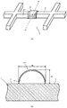
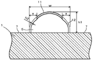
- FIG. 2 shows a perspective view (a) of the correction portion 5 obtained in this way and a cross-sectional view (b) of a portion corresponding to the A-A ′ line in this perspective view.
- an ink repellent surface 11 is formed on the entire surface of the correction portion 5 due to the characteristics of the curable correction liquid containing the ink repellent agent used above.
- the film thickness of the ink repellent surface 11 is preferably about 10 to 500 nm, more preferably 20 to 200 nm, although it depends on the curable correction liquid used.
- the height (h1) and width (w) of the modified hardened portion 5 are formed to be substantially the same as the height and width of the peripheral partition wall.
- the height h1 is preferably about 70 to 150% with respect to the height of the peripheral partition walls, and more preferably about 80 to 130%.
- the width w is preferably about 80 to 140% with respect to the width of the peripheral partition wall, and more preferably about 90 to 120%.
- the (4) laser light irradiation step schematically shown in FIG. 1 (d) is a surface (dots) continuous to the side surface of the partition wall of the correction portion 5 obtained in the step (3). This is a step of irradiating the surface near the boundary with 7 with the laser beam 9 and removing the surface layer of the correction portion 5 at the irradiated portion.
- the “surface continuous with the side wall of the partition wall” is formed in a shape that is continuous in a substantially horizontal direction with respect to the side surface 21 of the original partition wall 2 itself, for example, a hatched surface in FIG.
- the surface of the correction portion is a “surface continuous with the side surface of the partition wall” except for the surface that requires ink repellency that occupies a certain area in the upper portion of the correction portion.
- the laser light source (not shown), light having a pulse wave wavelength of 532 nm or 355 nm is preferable.
- the intensity of the laser beam used for irradiation is such an intensity that only the surface layer, which is the laser beam irradiation site, is removed in the correction unit 5 as described below, and the laser beam irradiation site can be visually confirmed. It adjusts suitably so that it may become intensity.
- FIG. 3 is a view showing a cross section of a correction portion obtained by an example of the method for correcting a partition wall of the present invention.
- the laser light irradiation is performed in a range from 2 to 10 ⁇ m from the outermost end of the correction portion 5 to the inside of the partition wall in consideration of the width of the partition wall of the article forming the pixel by the inkjet method (in FIG. 3). It is preferably performed on the surface (corresponding to the distance indicated by x), and this range is more preferably from 5 to 8 ⁇ m.
- the outermost end of the correction portion 5 refers to a portion where the correction portion protrudes most in the direction of the dot 7.
- the ink repellency of the upper surface of the partition correction part is not sufficiently ensured to the dots. There is a risk of color mixing when discharging the ink. Further, if the laser light irradiation range is less than 2 ⁇ m inward from the boundary with the dot, that is, if the distance x in FIG. 3 is less than 2 ⁇ m, the ink-philic part is not sufficiently formed, and the dot 7 When ink is ejected to the pixel, the pixel film thickness may become non-uniform (white spots).
- h2 / h1 ⁇ 0.5, where h1 is the maximum film thickness of the correction portion 5 before irradiation with laser light and h2 is the thickness of the surface layer removed by laser light irradiation. More preferably, h2 / h1 ⁇ 0.3. If h2 / h1 is 0.5 or more, the amount of splashing from the partition correction portion generated by laser light irradiation increases, and the ink repellency of the upper surface of the peripheral partition may be impaired. This is because when the ink-repellent surface 11 of the correction portion 5 is removed by being irradiated with laser light, the molecular chain is cut off and the ink-repellent surface 11 does not exhibit ink repellency. Furthermore, if the amount of splash from the partition correction portion increases, there is a concern about contamination of pixels formed later. Specifically, h2 is preferably 20 to 1,000 nm, and more preferably 30 to 500 nm.
- a surface layer is removed by laser light irradiation in an ink-repellent correction portion formed so as to efficiently and efficiently correct a chip defect of the partition wall and fill the chip.
- the surface continuing to the side wall of the partition wall has ink affinity. Therefore, it is possible to prevent color mixing of ink between adjacent pixels during ink ejection application for pixel formation by the inkjet method, and to obtain pixels with high film thickness uniformity.
- the above laser light irradiation removes only a small amount of the corrected cured product existing only on the surface layer of the corrected portion, so that a high-performance ink-discharge printed matter with less pixel contamination due to the splash of the corrected cured product removed.
- a color filter or an organic EL element can be provided.
- Examples 1, 3 and 4 are examples, and example 2 is a comparative example.
- “part” used as a compounding quantity of the compound in each example means “mass part”.
- the symbol of the compound used for each following example is shown next.
- MAA methacrylic acid
- 2-HEMA 2-hydroxyethyl methacrylate
- MMA methyl methacrylate
- 2-ME 2-mercaptoethanol
- V-70 2,2′-azobis (4-methoxy-2,4-dimethylvaleronitrile) (trade name: V-70, manufactured by Wako Pure Chemical Industries, Ltd.)
- MOI 2-methacryloyloxyethyl isocyanate
- DBTDL dibutyltin dilaurate
- BHT 2,6-di-t-butyl-p-cresol
- ZCR1569H biphenyl type epoxy acrylate (manufactured by Nippon Kayaku Co., Ltd., trade name: ZCR1569H, solid content 70% by mass)
- OXE02 Ethanone 1- [9-ethyl-6- (2-methylbenzoyl) -9H-carbazoyl-3-yl] -1- (O-acetyloxime) (trade name OXE02 manufactured by Ciba Specialty Chemicals)
- UX5002 urethane acrylate (manufactured by Nippon Kayaku Co., Ltd., trade name: KAYARAD UX5002)
- 157S65 Bisphenol A novolac type epoxy resin (manufactured by Japan Epoxy Resin, trade name: Epicoat 157S65)
- KBM403 3-glycidoxypropyltrimethoxysilane (manufactured by Shin-Etsu Chemical Co., Ltd., trade name: KBM-403)
- PGMEA propy
- polymer (1) 100 g
- MOI 47.7 g
- DBTDL 0.19 g
- BHT 2.4 g
- Acetone 100 g
- Water is added to the obtained acetone solution of the polymer (2) for reprecipitation purification, followed by reprecipitation purification with petroleum ether and vacuum drying to obtain 135 g of a polymer (A1) having a function as an ink repellent agent. It was.
- the weight average molecular weight was 8,800.
- Partition-forming composition Polymer (A1) (1.45 parts), ZCR1569H (47.1 parts) as a dispersion of an alkali-soluble photosensitive resin, OXE02 (8.7 parts) as a photopolymerization initiator, a dispersion of a black colorant CB (232.0 parts) as a radical crosslinking agent, UX5002 (31.8 parts), 157S65 (3.6 parts) as a thermosetting agent, KBM403 (5.8 parts) as a silane coupling agent, and PGMEA (570 parts) and CHON (100 parts) as a solvent were mixed to obtain a diluted solution of the partition wall forming composition.
- Partition correction fluid Polymer (A1) (0.21 part), UX5002 (28 parts) as a radical crosslinking agent, OXE02 (5.3 parts) as a photopolymerization initiator, CB (45 parts) as a dispersion of a black colorant, And MBA (21.49 parts) as a solvent and BDGAC (20 parts) were mixed to obtain a partition wall correction solution.
- Example 1 After applying a diluted solution of the partition wall forming composition on a non-alkali glass substrate using a slit coater, vacuum drying was performed at 130 Pa for 30 seconds, and further drying was performed on a hot plate at 100 ° C. for 2 minutes.
- a mask (line: 20 ⁇ m, lattice space: 100 ⁇ m ⁇ 200 ⁇ m) on which a lattice pattern was formed was placed above the coating film with a gap of 30 ⁇ m and irradiated with 100 mJ / cm 2 with an ultrahigh pressure mercury lamp.
- the substrate was developed using a 0.1% by mass tetramethylammonium hydroxide aqueous solution containing a surfactant at 25 ° C. for 40 seconds, washed with water, and dried to form a light-shielding partition.
- the apparatus is equipped with a defective partition wall observation unit for detecting a chip defect portion of the partition wall, a laser for removing the chip defect portion of the partition wall, and a micro dispenser for chip defect correction.
- the partition wall correction liquid obtained above was applied to the chip defect portion. This process was repeated twice, and the partition wall correction liquid was applied so that the partition walls were not chipped. Thereafter, the region where the barrier rib correction liquid was applied was irradiated with ultraviolet rays and cured to form a correction portion.
- the ultraviolet rays were irradiated with an exposure amount of 5,000 mJ / cm 2 by an ultraviolet spot irradiation apparatus using an ultrahigh pressure mercury lamp mounted on the apparatus as a light source.
- Laser wavelength 532 nm
- the film thickness maximum value (h1) in the corrected portion before laser-light irradiation was 1.9 ⁇ m
- the film thickness (h2) shaved by irradiation with a pulsed laser was It was 200 nm and h2 / h1 was 0.1.
- thermosetting ink 180 pL containing a green pigment and having a solid content of 25% was injected using an ink jet apparatus. Dry on a hot plate at 100 ° C. for 5 minutes. Next, heat treatment was performed at 200 ° C. for 30 minutes to form pixels. The volume of the ink layer after heat curing was 40 pL.
- the upper surface of the partition wall in the correction portion has ink repellency, and the surface continuous with the side surface of the partition wall in the correction portion has ink affinity, so that the ink overflows from the partition wall.
- An ink layer could be formed with high definition without causing defects such as white spots due to color mixing or ink repelling around the partition walls.
- Example 2 In the same manner as in Example 1, a light-shielding partition was formed on an alkali-free glass substrate. When defects were detected in the same manner as in Example 1 for the partition walls, chip defects were detected. In the same manner as in Example 1, the partition wall correction liquid was applied to the chip defect portion and cured to obtain a correction portion. The modified part of the partition wall was subjected to the following pixel formation as it was after curing without performing the laser treatment as in Example 1 above. A thermosetting ink (180 pL) containing a green pigment and having a solid content of 25% was injected into an area of 100 ⁇ m ⁇ 200 ⁇ m partitioned by the partition wall having the correction part, using an inkjet apparatus. Dry on a hot plate at 100 ° C. for 5 minutes. Next, heat treatment was performed at 200 ° C. for 30 minutes to form pixels. The volume of the ink layer after heat curing was 40 pL.
- a surface continuous to the side surface of the partition wall in the correction portion has ink repellency, and thus white spots occurred due to ink repelling around the side wall of the correction portion.
- Example 3 In the same manner as in Example 1, a light-shielding partition was formed on an alkali-free glass substrate. When defects were detected in the same manner as in Example 1 for the partition walls, chip defects were detected. In the same manner as in Example 1, the partition wall correction liquid was applied to the chip defect portion and cured to obtain a correction portion. In order to remove the ink repellency of the surface continuous with the side surface of the partition wall in the correction portion, a pulse having a width of 5 ⁇ m from the outermost end of the correction portion (x in FIG. 3 corresponds to 5 ⁇ m) is applied to this surface of the correction portion. Laser (wavelength 532 nm) was irradiated with a laser output of 60%.
- the maximum film thickness value (h1) was 2.0 ⁇ m
- the film thickness (h2) shaved by irradiation with a pulse laser was 0.8 ⁇ m
- h2 / h1 was 0.4.
- thermosetting ink 180 pL containing a green pigment and having a solid content of 25% was injected using an ink jet apparatus. Dry on a hot plate at 100 ° C. for 5 minutes. Next, heat treatment was performed at 200 ° C. for 30 minutes to form pixels. The volume of the ink layer after heat curing was 40 pL.
- the upper surface of the partition wall in the correction portion has ink repellency, and the surface continuous with the side surface of the partition wall in the correction portion has ink affinity, so that the ink overflows from the partition wall.
- An ink layer could be formed with high definition without causing defects such as white spots due to color mixing or ink repelling around the partition walls.
- Example 4 In the same manner as in Example 1, a light-shielding partition was formed on an alkali-free glass substrate. When defects were detected in the same manner as in Example 1 for the partition walls, chip defects were detected. In the same manner as in Example 1, the partition wall correction liquid was applied to the chip defect portion and cured to obtain a correction portion. In order to remove the ink repellency of the surface continuous with the side surface of the partition wall in the correction portion, a pulse having a width of 5 ⁇ m from the outermost end of the correction portion (x in FIG. 3 corresponds to 5 ⁇ m) is applied to this surface of the correction portion. Laser (wavelength 532 nm) was irradiated with 100% laser power.
- the maximum film thickness value (h1) was 2.0 ⁇ m
- the film thickness (h2) shaved by irradiation with a pulse laser was 1.2 ⁇ m
- h2 / h1 was 0.6.
- thermosetting ink 180 pL containing a green pigment and having a solid content of 25% was injected into an area of 100 ⁇ m ⁇ 200 ⁇ m partitioned by the partition wall having the correction part, using an inkjet device. Dry on a hot plate at 100 ° C. for 5 minutes. Next, heat treatment was performed at 200 ° C. for 30 minutes to form pixels. The volume of the ink layer after heat curing was 40 pL.
- the amount of splash from the partition correction portion increased, and the ink repellency of the upper surface of the partition was lowered, so that the ink was running on the upper portion of the partition.
- h2 / h1 exceeded 0.5, it was confirmed that the ink repellency on the upper surface of the partition wall was insufficient, and if h2 / h1 ⁇ 0.5, better ink repellency could be expressed.
- a defect defect that occurs on a partition wall formed on a substrate so as to partition a plurality of pixels and having ink repellency on the upper surface and ink affinity on the side surface is corrected.
- the ink ejection for pixel formation performed after the correction only the surface corresponding to the upper part of the partition wall is modified to have ink repellency. Therefore, it is possible to prevent the pixel film thickness from becoming non-uniform and applicable to partition walls used for color filters, organic EL elements, circuit boards, thin film transistors, microlenses, biochips, and the like.
Landscapes
- Physics & Mathematics (AREA)
- General Physics & Mathematics (AREA)
- Optics & Photonics (AREA)
- Engineering & Computer Science (AREA)
- Microelectronics & Electronic Packaging (AREA)
- Manufacturing & Machinery (AREA)
- Electroluminescent Light Sources (AREA)
- Optical Filters (AREA)
Abstract
Description
例えば、カラーフィルタの製造においては、撥液性を有する隔壁を形成した後に、隔壁で区画された画素領域にR(レッド)、G(グリーン)、B(ブルー)のインクをインクジェット法により塗布し、着色層を有する画素が形成される。
また、有機EL表示素子の製造においては、撥液性を有する隔壁を形成した後に、隔壁で区画された画素領域に正孔輸送材料、および発光材料の溶液であるインクをインクジェット法により塗布し、正孔輸送層、発光層等を有する画素が形成される。
有機EL表示素子の製造において、隔壁に欠け欠陥がある場合、その欠陥を介して隣接するドットに塗布された異なる発色をするインクどうしが接触すること等により、混色が生じることがある。また、同じインクのみを製膜する場合においても、インクの膜厚制御が困難となる。
この問題を解決して修正部に撥インク性をもたせながら精度よく隔壁を修正する方法として、例えば、特許文献1には、隔壁の欠け欠陥について、修正箇所に下塗り層を形成させた後に撥インク剤を含むリペアインクで修正する技術が提案されている。
[1]基板上に複数の区画を形成するために、前記基板上に配設された、上面に撥インク性を有し側面に親インク性を有する隔壁の欠け欠陥を修正する方法であって、前記隔壁の欠け欠陥を検出する工程、前記欠け欠陥に対して撥インク剤を含む硬化性修正液を該修正液が硬化した際に少なくとも前記欠け欠陥が充填され、かつ周辺隔壁とほぼ同じ大きさとなるように、塗工する工程、前記硬化性修正液を硬化させて修正部とする工程、および前記修正部の、前記隔壁の側面に連続した面にレーザー光を照射し、照射部位において前記修正部の表層を除去する工程、を有することを特徴とする、上面に撥インク性を有し側面に親インク性を有する隔壁の欠け欠陥の修正方法。
[3]前記隔壁が、
基板上に撥インク剤を含む感光性樹脂組成物を塗布し、該感光性樹脂組成物の塗膜の層を形成し、
次に、所望のパターンに対応するマスクを介して、前記塗膜の層に光を照射し、光が照射された部分を硬化させ、
次に、現像処理を行い、光が照射されなかった部分を除去して、
得られた隔壁である、[1]または[2]に記載の修正方法。
[4]前記感光性樹脂組成物が、さらに光ラジカル重合性のバインダー樹脂、および光重合開始剤を含む、[3]に記載の修正方法。
[5]前記撥インク剤が、フルオロアルキル基とエチレン性二重結合を側鎖に有するポリマーである、[3]または[4]に記載の修正方法。
[6]前記レーザー光の照射が、前記修正部の最外端から隔壁の内側に向かって2~10μmの領域の表面に対して行われる、[1]~[5]のいずれかに記載の修正方法。
[7]前記硬化性修正液が含フッ素撥インク剤を含む、[1]~[6]のいずれかに記載の修正方法
[8]前記含フッ素撥インク剤がエチレン性二重結合を含む、[7]に記載の修正方法。
[10]前記隔壁が遮光性を有する隔壁である、[1]~[9]のいずれかに記載の修正方法。
[11]前記隔壁がカラーフィルタ用の隔壁である、[1]~[10]のいずれかに記載の修正方法。
[12]前記隔壁が有機EL素子用の隔壁である、[1]~[11]のいずれかに記載の修正方法。
(1)前記隔壁の欠け欠陥を検出する工程(以下、「欠け欠陥検出工程」という)
(2)前記欠け欠陥に対して撥インク剤を含む硬化性修正液を該修正液が硬化した際に少なくとも前記欠け欠陥が充填され、かつ周辺隔壁とほぼ同じ大きさとなるように、塗工する工程(以下、「塗工工程」という)
(3)前記硬化性修正液を硬化させて修正部とする工程(以下、「硬化工程」という)
(4)前記修正部の、前記隔壁の側面に連続した面にレーザー光を照射し、照射部位において前記修正部の表層を除去する工程(以下、「レーザー光照射工程」という)
この(1)欠け欠陥検出工程は、基板1上を複数のドット7に仕切るように形成された隔壁2において、図1(a)に示すような修正すべき欠け欠陥3を検出する工程である。基板1上の隔壁2に存在する欠け欠陥3を検出する方法としては、通常、このような隔壁から欠け欠陥を検出するのに用いる方法を特に制限なく用いることができる。
(a)基板上に撥インク剤を含む感光性樹脂組成物を塗布し、該感光性樹脂組成物の塗膜の層を形成する。
(b)所望のパターンに対応するマスクを介して、前記塗膜の層に紫外線等の光を照射し、光が照射された部分を硬化させる。
(c)現像処理を行い、光が照射されなかった部分を除去する。
上記撥インク剤の好ましい態様の一つであるフルオロアルキル基を側鎖に有するポリマーの製造方法としては、特開2000-102727号公報、特開2002-249706号公報等に開示されている方法を参照することが可能である。
本発明に用いる感光性樹脂組成物は、隔壁が、例えば、ブラックマトリックスのような遮光性を有する隔壁である場合には、遮光性粒子を含有することが好ましい。これにより、隔壁に遮光性を付与できる。
さらに、カーボンブラックの平均1次粒子径は、20~50nmであることが好ましく、25~45nmがより好ましい。カーボンブラックの平均1次粒子径が当該範囲の下限値以上であると、高濃度に分散させやすく、経時安定性の良好な感光性黒色組成物が得やすい。当該範囲の上限値以下であると、ブラックマトリックス等の遮光性隔壁の形状の劣化を招きにくい。なお、カーボンブラックの平均1次粒子径は、電子顕微鏡等による目視等で測定できる。
上記希釈剤の添加量としては、感光性樹脂組成物全量に対して50~95質量%、好ましくは70~90質量%となる量を、感光性樹脂組成物の塗装性の観点から好ましい量として挙げることができる。
上記(1)で検出された欠け欠陥に対して、撥インク剤を含む硬化性修正液を、この修正液が硬化した際に少なくとも欠け欠陥が充填され、かつ周辺隔壁とほぼ同じ大きさ(高さおよび幅)となるように、塗工する。
本発明に用いる硬化性修正液は、撥インク性を得るために撥インク剤を含有する。また、塗工後、硬化性修正液を硬化した際に、少なくとも欠け欠陥が充填され、周辺隔壁と同等の大きさになるように塗工することが可能な塗工性能を有する。
硬化性修正液は、上記の隔壁そのものを形成するための感光性樹脂組成物と同じであってもよいが、光や熱によって硬化させて用いるため、通常はネガ型の組成物である。さらに、隔壁を修正するにあたっては現像工程を行わないため、アルカリ可溶性樹脂を含まない組成物とすることが好ましい。硬化性修正液は、撥インク剤、ラジカル架橋剤、および光重合開始剤を含む組成物であることが好ましい。
撥インク剤としては、硬化性修正液から得られる硬化物の表面に撥インク性を付与できるものであれば特に制限されない。前記感光性樹脂組成物に含まれる撥インク剤と同様のものが採用でき、好ましい態様も同様である。
本発明に用いる硬化性修正液は、上記撥インク剤、好ましくは含フッ素撥インク剤の他に、2個以上のエチレン性二重結合を有するラジカル架橋剤を含むことが好ましい。これにより、硬化性修正液の光硬化性が向上し、修正された隔壁には、その後のインクジェット法により画素形成用のインクの塗布プロセスに耐えうる充分な耐薬品性が付与される。
本発明に用いる硬化性修正液は、さらに、光重合開始剤を含むことが好ましい。光重合開始剤は、光によりラジカルを発生する化合物からなることが好ましい。光重合開始剤としては、前記感光性樹脂組成物中に含まれる光重合開始剤と同様のものが挙げられ、好ましい態様も同様である。
本発明に用いる硬化性修正液は、修正する隔壁が、例えば、ブラックマトリックスのような遮光性を有する隔壁である場合には、遮光性粒子を含有することが好ましい。これにより、硬化性修正液が硬化した修正硬化物からなる隔壁修正部に遮光性を付与することができる。遮光性粒子としては、上記感光性樹脂組成物が含みうる遮光性粒子と同様のものが挙げられ、好ましい態様も同様である。
硬化性修正液は、耐久性や耐薬品性の向上を目的として熱硬化剤を含むことが好ましい。熱硬化剤としては、例えば、アミノ樹脂、2個以上のエポキシ基を有する化合物、2個以上のヒドラジノ基を有する化合物、ポリカルボジイミド化合物、2個以上のオキサゾリン基を有する化合物、2個以上のアジリジン基を有する化合物、多価金属類、2個以上のメルカプト基を有する化合物、ポリイソシアネート化合物等が挙げられる。
硬化性修正液は、必要に応じて硬化促進剤、増粘剤、可塑剤、消泡剤、レベリング剤、ハジキ防止剤、紫外線吸収剤等を含んでもよい。
上記反応性官能基を有するモノマーとしては、エチレン性不飽和結合、エポキシ基、オキサゾリン基、環状尿素基、環状エステル基等を有するモノマーが挙げられる。安定性と反応性の観点から、エチレン性不飽和結合、またはエポキシ基を有するモノマーが好ましい。また、反応性官能基を有するモノマーは単官能であることが好ましい。
撥インク剤を硬化性修正液の全固形分に対して0.01~30質量%、
ラジカル架橋剤を硬化性修正液の全固形分に対して40~80質量%、
光重合開始剤を硬化性修正液の全固形分に対して0.1~50質量%、
遮光性粒子としてのカーボンブラックを、硬化性修正液の全固形分に対して15~50質量%、
溶媒:MBAおよび/またはBDGACを、硬化性修正液の全量(100質量部)に対して10~80質量部、
である。
本発明の隔壁修正方法においては、上記各種成分を含有する硬化性修正液を調製し、上記(1)で検出された欠け欠陥に対して、この修正液が硬化した際に少なくとも欠け欠陥が充填され、かつ周辺隔壁とほぼ同じ大きさ(高さおよび幅)となるように、塗工する。
本発明の隔壁修正方法において、上記(2)塗工工程で、隔壁2の欠け欠陥3の位置に、この修正液が硬化した際に少なくとも欠け欠陥が充填され、かつ周辺隔壁とほぼ同じ大きさ(高さおよび幅)となるように、塗工した硬化性修正液は、次いでこの(3)硬化工程により硬化し修正部となる。なお、この硬化の前に必要に応じて以下の乾燥工程を設けてもよい。
硬化性修正液4を塗布した後、硬化性修正液4に溶剤が含まれない場合は、乾燥を行う必要はない。なお、硬化性修正液4に溶剤が含まれていても自然に溶剤が揮発することがある。乾燥を行う場合には、風乾、加熱乾燥、真空乾燥等を行えばよい。加熱乾燥の場合、オーブン、ホットプレート等を使用し、50~300℃の範囲で1分間~3時間行うのが好ましい。また、隔壁2の修正においては局所的かつ短時間での乾燥が要求されることが多いので、赤外線スポットヒーター等を用いて、修正箇所だけを加熱して乾燥する方法も好ましく用いられる。
上記必要に応じて行われる乾燥の後、硬化性修正液4を硬化させる。硬化の方法としては、硬化性修正液4が充分に硬化する方法であれば、特に限定はないが、紫外線照射によって硬化させる方法が好ましい。図1(c)は、この紫外線8照射による硬化工程を、模式的に示すものである。光源としては、高圧水銀ランプ、超高圧水銀ランプ、水銀キセノンランプ、レーザー光線等を用いることができる。特に、発光照度を上げるために、光を集光させた超高圧水銀ランプの水銀キセノンランプスポット光源が好ましい。このような紫外線8を発光するスポット光源(図示せず)を用いると、その発光照度が高いため、短時間で修正液を硬化させるのに充分なエネルギーを照射することができ、また、修正箇所のみを照射できるため、生産性が高い。
図1(d)に模式的に示す(4)レーザー光照射工程は、上記(3)工程で得られた、修正部5の、隔壁の側面に連続した面(ドット7との境界近傍における表面)にレーザー光9を照射し、この照射部位において修正部5の表層を除去する工程である。この「隔壁の側面に連続した面」とは、例えば、図2(a)で斜線を施した面のように、もともとの隔壁2自身の側面21に対して略水平方向に連続するかたちに形成された修正部の側面であって後のインク吐出工程においてインクと接しうる面であり、撥インク性を有する隔壁の上面から連続するかたちに形成された修正部上部の面とは区別される。言い換えれば、修正部上部に一定面積占める撥インク性が必要とされる面を除く、修正部の表面が「隔壁の側面に連続した面」となる。
なお、具体的には、h2は20~1,000nmであることが好ましく、30~500nmがより好ましい。
また、上記レーザー光照射によっては、修正部の端部表層のみに存在する少量の修正硬化物しか除去しないため、除去された修正硬化物の飛沫による画素の汚染が少ない、高性能なインク吐出印刷物、例えば、カラーフィルタや有機EL素子を提供できる。
MAA:メタクリル酸、
2-HEMA:2-ヒドロキシエチルメタクリレート、
MMA:メチルメタクリレート、
2-ME:2-メルカプトエタノール、
V-70:2,2’-アゾビス(4-メトキシ-2,4-ジメチルバレロニトリル)(和光純薬社製、商品名:V-70)、
MOI:2-メタクリロイルオキシエチルイソシアネート、
DBTDL:ジブチル錫ジラウレート、
BHT:2,6-ジ-t-ブチル-p-クレゾール、
OXE02:エタノン 1-[9-エチル-6-(2-メチルベンゾイル)-9H-カルバゾイル-3-イル]-1-(O-アセチルオキシム)(チバスペシャルティケミカルズ社製、商品名OXE02)、
UX5002:ウレタンアクリレート(日本化薬社製、商品名:KAYARAD UX5002)、
157S65:ビスフェノールAノボラック型エポキシ樹脂(ジャパンエポキシレジン社製、商品名:エピコート157S65)、
KBM403:3-グリシドキシプロピルトリメトキシシラン(信越化学工業社製、商品名:KBM-403)、
PGMEA:プロピレングリコールモノメチルエーテルアセテート、
CHON:シクロヘキサノン、
MBA:3-メトキシブチルアセテート、
BDGAC:ジエチレングリコールモノブチルエーテルアセテート、
CB:カーボンブラック(平均二次粒径:120nm、プロピレングリコールモノメチルエーテルアセテート溶液、CB分20質量%、固形分25質量%)。
[合成例1]
撹拌機を備えた内容積1Lのオートクレーブに、アセトン(556g)、C6FMA(96g)、MAA(4.8g)、2-HEMA(96g)、MMA(43.2g)、連鎖移動剤2-ME(6.2g)および重合開始剤V-70(4.5g)を仕込み、窒素ガス中で撹拌しながら、40℃で18時間重合させ、重合体(1)の溶液を得た。得られた重合体(1)のアセトン溶液に水を加え再沈精製し、次いで石油エーテルで再沈精製し、真空乾燥し、重合体(1)の237gを得た。
重合体(A1)(1.45部)、アルカリ可溶性感光性樹脂の分散液としてのZCR1569H(47.1部)、光重合開始剤としてのOXE02(8.7部)、黒色着色剤の分散液としてのCB(232.0部)、ラジカル架橋剤としてのUX5002(31.8部)、熱硬化剤としての157S65(3.6部)、シランカップリング剤としてのKBM403(5.8部)および溶剤としてのPGMEA(570部)およびCHON(100部)を混合して、隔壁形成用組成物の希釈液を得た。
重合体(A1)(0.21部)、ラジカル架橋剤としてのUX5002(28部)、光重合開始剤としてのOXE02(5.3部)黒色着色剤の分散液としてのCB(45部)、および溶剤としてのMBA(21.49部)、BDGAC(20部)を混合して、隔壁修正液を得た。
無アルカリガラス基板上にスリットコーターを用いて、隔壁形成用組成物の希釈液を塗布した後、130Paで30秒間真空乾燥を行い、さらに100℃で2分間ホットプレート上で乾燥した。塗膜の上方に、格子パターンが形成されているマスク(ライン:20μm、格子スペース:100μm×200μm)を30μmのギャップで設置し、超高圧水銀灯により100mJ/cm2を照射した。次いで基板を界面活性剤入り0.1質量%テトラメチルアンモニウムヒドロキシド水溶液を用い、25℃で40秒間現像処理を行い、水で洗浄し、乾燥させ、遮光性隔壁を形成した。
例1と同様にして、無アルカリガラス基板上に遮光性隔壁を形成した。この隔壁について例1と同様にして、欠陥の検出を行ったところ、欠け欠陥が検出された。例1と同様にして、欠け欠陥部に隔壁修正液を塗布し硬化させて修正部とした。この隔壁の修正部に対しては、上記例1のようなレーザー処理を行うことなく、硬化後、そのまま以下の画素形成を行った。
上記修正部を有する隔壁で区画された100μm×200μmの領域内に、インクジェット装置を用いて、緑色の顔料を含んだ固形分25%の熱硬化型インク(180pL)を注入した。100℃で5分間ホットプレート上で乾燥した。次いで200℃で30分間加熱処理を行い、画素を形成した。インク層の加熱硬化後の体積は40pLであった。
例1と同様にして、無アルカリガラス基板上に遮光性隔壁を形成した。この隔壁について例1と同様にして、欠陥の検出を行ったところ、欠け欠陥が検出された。例1と同様にして、欠け欠陥部に隔壁修正液を塗布し硬化させて修正部とした。
修正部において、隔壁の側面に連続した面の撥インク性を除去するために、修正部のこの面に、修正部の最外端から5μm幅で(図3のxが5μmに相当する)パルスレーザー(波長532nm)を60%のレーザー出力で照射した。光学顕微鏡にて膜厚を測定したところ、膜厚最大値(h1)は2.0μm、パルスレーザーを照射されて削れた膜厚(h2)は0.8μmであり、h2/h1は0.4であった。
例1と同様にして、無アルカリガラス基板上に遮光性隔壁を形成した。この隔壁について例1と同様にして、欠陥の検出を行ったところ、欠け欠陥が検出された。例1と同様にして、欠け欠陥部に隔壁修正液を塗布し硬化させて修正部とした。
修正部において、隔壁の側面に連続した面の撥インク性を除去するために、修正部のこの面に、修正部の最外端から5μm幅で(図3のxが5μmに相当する)パルスレーザー(波長532nm)を100%のレーザー出力で照射した。光学顕微鏡にて膜厚を測定したところ、膜厚最大値(h1)は2.0μm、パルスレーザーを照射されて削れた膜厚(h2)は1.2μmであり、h2/h1は0.6であった。
h2/h1が0.5を超えると、隔壁上部表面の撥インク性が不充分であり、h2/h1<0.5であればより良好な撥インク性を発現できることを確認した。
なお、2010年4月13日に出願された日本特許出願2010-092219号の明細書、特許請求の範囲、図面及び要約書の全内容をここに引用し、本発明の明細書の開示として、取り入れるものである。
Claims (12)
- 基板上に複数の区画を形成するために、前記基板上に配設された、上面に撥インク性を有し側面に親インク性を有する隔壁の欠け欠陥を修正する方法であって、
前記隔壁の欠け欠陥を検出する工程、
前記欠け欠陥に対して撥インク剤を含む硬化性修正液を該修正液が硬化した際に少なくとも前記欠け欠陥が充填され、かつ周辺隔壁とほぼ同じ大きさとなるように、塗工する工程、
前記硬化性修正液を硬化させて修正部とする工程、および
前記修正部の、前記隔壁の側面に連続した面にレーザー光を照射し、照射部位において前記修正部の表層を除去する工程、
を有することを特徴とする、上面に撥インク性を有し側面に親インク性を有する隔壁の欠け欠陥の修正方法。 - 前記レーザー光を照射する前の修正部の膜厚最大値をh1、レーザー光照射によって除去される表層の厚さをh2とするとき、h2/h1<0.5である、請求項1に記載の修正方法。
- 前記隔壁が、
基板上に撥インク剤を含む感光性樹脂組成物を塗布し、該感光性樹脂組成物の塗膜の層を形成し、
次に、所望のパターンに対応するマスクを介して、前記塗膜の層に光を照射し、光が照射された部分を硬化させ、
次に、現像処理を行い、光が照射されなかった部分を除去して、
得られた隔壁である、請求項1または2に記載の修正方法。 - 前記感光性樹脂組成物が、さらに光ラジカル重合性のバインダー樹脂、および光重合開始剤を含む、請求項3に記載の修正方法。
- 前記撥インク剤が、フルオロアルキル基とエチレン性二重結合を側鎖に有するポリマーである、請求項1~4のいずれか1項に記載の修正方法。
- 前記レーザー光の照射が、前記修正部の最外端から隔壁の内側に向かって2~10μmの領域の表面に対して行われる、請求項1~5のいずれか1項に記載の修正方法。
- 前記硬化性修正液が含フッ素撥インク剤を含む、請求項1~6のいずれか1項に記載の修正方法
- 前記含フッ素撥インク剤がエチレン性二重結合を含む、請求項7に記載の修正方法。
- 前記硬化性修正液が、さらにラジカル架橋剤および光重合開始剤を含む、請求項7または8に記載の修正方法。
- 前記隔壁が遮光性を有する隔壁である、請求項1~9のいずれか1項に記載の修正方法。
- 前記隔壁がカラーフィルタ用の隔壁である、請求項1~10のいずれか1項に記載の修正方法。
- 前記隔壁が有機EL素子用の隔壁である、請求項1~11のいずれか1項に記載の修正方法。
Priority Applications (2)
| Application Number | Priority Date | Filing Date | Title |
|---|---|---|---|
| JP2012510643A JPWO2011129283A1 (ja) | 2010-04-13 | 2011-04-08 | 隔壁の修正方法 |
| KR1020127016374A KR20130049170A (ko) | 2010-04-13 | 2011-04-08 | 격벽의 수정 방법 |
Applications Claiming Priority (2)
| Application Number | Priority Date | Filing Date | Title |
|---|---|---|---|
| JP2010092219 | 2010-04-13 | ||
| JP2010-092219 | 2010-04-13 |
Publications (1)
| Publication Number | Publication Date |
|---|---|
| WO2011129283A1 true WO2011129283A1 (ja) | 2011-10-20 |
Family
ID=44798659
Family Applications (1)
| Application Number | Title | Priority Date | Filing Date |
|---|---|---|---|
| PCT/JP2011/058935 Ceased WO2011129283A1 (ja) | 2010-04-13 | 2011-04-08 | 隔壁の修正方法 |
Country Status (4)
| Country | Link |
|---|---|
| JP (1) | JPWO2011129283A1 (ja) |
| KR (1) | KR20130049170A (ja) |
| TW (1) | TW201202758A (ja) |
| WO (1) | WO2011129283A1 (ja) |
Cited By (7)
| Publication number | Priority date | Publication date | Assignee | Title |
|---|---|---|---|---|
| WO2015133090A1 (ja) * | 2014-03-07 | 2015-09-11 | 株式会社Joled | バンクの補修方法、有機el表示装置およびその製造方法 |
| WO2016047021A1 (ja) * | 2014-09-24 | 2016-03-31 | 株式会社Joled | 有機el表示装置の製造方法および有機el表示装置 |
| US9818809B2 (en) | 2014-02-10 | 2017-11-14 | Joled Inc. | Bank repair for organic EL display device |
| CN111834534A (zh) * | 2019-04-17 | 2020-10-27 | 三星显示有限公司 | 显示装置及其制造方法 |
| JP2020182948A (ja) * | 2014-10-24 | 2020-11-12 | Agc株式会社 | 隔壁の修復方法、修復された隔壁、および光学素子 |
| WO2021256441A1 (ja) * | 2020-06-17 | 2021-12-23 | Agc株式会社 | 隔壁用硬化性組成物、隔壁の修復方法、隔壁、および光学素子 |
| WO2021256440A1 (ja) * | 2020-06-17 | 2021-12-23 | Agc株式会社 | 隔壁用硬化性組成物、隔壁の修復方法、隔壁、および光学素子 |
Families Citing this family (1)
| Publication number | Priority date | Publication date | Assignee | Title |
|---|---|---|---|---|
| CN109143631B (zh) * | 2018-09-30 | 2020-11-20 | 惠科股份有限公司 | 修补方法及装置 |
Citations (5)
| Publication number | Priority date | Publication date | Assignee | Title |
|---|---|---|---|---|
| JP2002022933A (ja) * | 2000-07-13 | 2002-01-23 | Canon Inc | 光学素子とその製造方法、液晶素子 |
| JP2006072176A (ja) * | 2004-09-06 | 2006-03-16 | Seiko Epson Corp | バンク、カラーフィルタ、表示装置及び電子機器 |
| WO2006035621A1 (ja) * | 2004-09-29 | 2006-04-06 | Sharp Kabushiki Kaisha | カラーフィルタ基板、液晶表示装置、カラーフィルタ基板の製造方法、及び、液晶表示装置の製造方法 |
| JP2009104030A (ja) * | 2007-10-25 | 2009-05-14 | Toppan Printing Co Ltd | インキ吐出印刷物の修正方法及び印刷物 |
| WO2010013654A1 (ja) * | 2008-07-30 | 2010-02-04 | 旭硝子株式会社 | 隔壁と画素が形成された基板を製造する方法 |
-
2011
- 2011-04-08 KR KR1020127016374A patent/KR20130049170A/ko not_active Withdrawn
- 2011-04-08 WO PCT/JP2011/058935 patent/WO2011129283A1/ja not_active Ceased
- 2011-04-08 JP JP2012510643A patent/JPWO2011129283A1/ja active Pending
- 2011-04-12 TW TW100112635A patent/TW201202758A/zh unknown
Patent Citations (5)
| Publication number | Priority date | Publication date | Assignee | Title |
|---|---|---|---|---|
| JP2002022933A (ja) * | 2000-07-13 | 2002-01-23 | Canon Inc | 光学素子とその製造方法、液晶素子 |
| JP2006072176A (ja) * | 2004-09-06 | 2006-03-16 | Seiko Epson Corp | バンク、カラーフィルタ、表示装置及び電子機器 |
| WO2006035621A1 (ja) * | 2004-09-29 | 2006-04-06 | Sharp Kabushiki Kaisha | カラーフィルタ基板、液晶表示装置、カラーフィルタ基板の製造方法、及び、液晶表示装置の製造方法 |
| JP2009104030A (ja) * | 2007-10-25 | 2009-05-14 | Toppan Printing Co Ltd | インキ吐出印刷物の修正方法及び印刷物 |
| WO2010013654A1 (ja) * | 2008-07-30 | 2010-02-04 | 旭硝子株式会社 | 隔壁と画素が形成された基板を製造する方法 |
Cited By (16)
| Publication number | Priority date | Publication date | Assignee | Title |
|---|---|---|---|---|
| US9818809B2 (en) | 2014-02-10 | 2017-11-14 | Joled Inc. | Bank repair for organic EL display device |
| WO2015133090A1 (ja) * | 2014-03-07 | 2015-09-11 | 株式会社Joled | バンクの補修方法、有機el表示装置およびその製造方法 |
| JPWO2015133090A1 (ja) * | 2014-03-07 | 2017-04-06 | 株式会社Joled | バンクの補修方法、有機el表示装置およびその製造方法 |
| US9837640B2 (en) | 2014-03-07 | 2017-12-05 | Joled Inc. | Method for repairing bank, organic EL display device, and method for manufacturing same |
| WO2016047021A1 (ja) * | 2014-09-24 | 2016-03-31 | 株式会社Joled | 有機el表示装置の製造方法および有機el表示装置 |
| JPWO2016047021A1 (ja) * | 2014-09-24 | 2017-06-29 | 株式会社Joled | 有機el表示装置の製造方法および有機el表示装置 |
| US10243176B2 (en) | 2014-09-24 | 2019-03-26 | Joled Inc. | Method for manufacturing organic EL display device and organic EL display device |
| JP2020182948A (ja) * | 2014-10-24 | 2020-11-12 | Agc株式会社 | 隔壁の修復方法、修復された隔壁、および光学素子 |
| CN111834534A (zh) * | 2019-04-17 | 2020-10-27 | 三星显示有限公司 | 显示装置及其制造方法 |
| CN111834534B (zh) * | 2019-04-17 | 2025-04-22 | 三星显示有限公司 | 显示装置及其制造方法 |
| WO2021256441A1 (ja) * | 2020-06-17 | 2021-12-23 | Agc株式会社 | 隔壁用硬化性組成物、隔壁の修復方法、隔壁、および光学素子 |
| WO2021256440A1 (ja) * | 2020-06-17 | 2021-12-23 | Agc株式会社 | 隔壁用硬化性組成物、隔壁の修復方法、隔壁、および光学素子 |
| JPWO2021256441A1 (ja) * | 2020-06-17 | 2021-12-23 | ||
| CN115918259A (zh) * | 2020-06-17 | 2023-04-04 | Agc株式会社 | 隔壁用固化性组合物、隔壁的修复方法、隔壁和光学元件 |
| JP7663098B2 (ja) | 2020-06-17 | 2025-04-16 | Agc株式会社 | 隔壁用硬化性組成物、隔壁の修復方法、隔壁、および光学素子 |
| TWI889848B (zh) * | 2020-06-17 | 2025-07-11 | 日商Agc股份有限公司 | 阻隔壁用硬化性組合物、阻隔壁之修復方法、阻隔壁、及光學元件 |
Also Published As
| Publication number | Publication date |
|---|---|
| TW201202758A (en) | 2012-01-16 |
| JPWO2011129283A1 (ja) | 2013-07-18 |
| KR20130049170A (ko) | 2013-05-13 |
Similar Documents
| Publication | Publication Date | Title |
|---|---|---|
| JPWO2011129283A1 (ja) | 隔壁の修正方法 | |
| JP5093352B2 (ja) | ネガ型感光性組成物、それを用いた光学素子用隔壁および該隔壁を有する光学素子 | |
| JP4930378B2 (ja) | 隔壁、カラーフィルタ、有機elの製造方法 | |
| JPWO2010134550A1 (ja) | 光学素子の製造方法 | |
| WO2018225782A1 (ja) | 量子ドット含有硬化性組成物、量子ドット含有硬化物、光学部材の製造方法、及び表示装置の製造方法 | |
| KR101981579B1 (ko) | 표시장치용 감광성 조성물, 이를 포함하는 블랙 매트릭스 및 블랙 매트릭스의 패턴 형성 방법 | |
| JPWO2010013654A1 (ja) | 隔壁と画素が形成された基板を製造する方法 | |
| KR101787651B1 (ko) | 알칼리 현상성 감광성 수지 조성물, 및 이것을 이용해서 형성한 표시소자용 격벽, 그리고 표시소자 | |
| JP2019179111A (ja) | 表示素子用積層体、及び隔壁形成用組成物 | |
| CN107113937A (zh) | 分隔壁用固化性组合物、分隔壁、分隔壁的制造方法、分隔壁的修复方法、经修复的分隔壁、以及光学元件 | |
| CN103178213B (zh) | 有机发光显示装置及其制造方法 | |
| JP2010164965A (ja) | カラーフィルタ画素形成用組成物、カラーフィルタ、液晶表示装置及び有機elディスプレイ | |
| JPWO2008146855A1 (ja) | 感光性組成物、隔壁、ブラックマトリックス | |
| JP2011039404A (ja) | 光学素子隔壁形成用感光性組成物、これを用いたブラックマトリックスおよびその製造方法、並びにカラーフィルタの製造方法 | |
| JP2008298859A (ja) | 感光性組成物、それを用いた隔壁、隔壁の製造方法、カラーフィルタの製造方法、有機el表示素子の製造方法および有機tftアレイの製造方法 | |
| WO2013031737A1 (ja) | ネガ型感光性樹脂組成物、隔壁および光学素子 | |
| JPWO2008149776A1 (ja) | 隔壁と画素が形成された基板を製造する方法 | |
| JPWO2019182041A1 (ja) | 硬化膜の製造方法、及び有機elディスプレイの製造方法 | |
| JP2009104030A (ja) | インキ吐出印刷物の修正方法及び印刷物 | |
| TWI440903B (zh) | 濾色器間隔壁形成用感光性樹脂組成物與使用該樹脂組成物形成之濾色器間隔壁,及濾色器與濾色器的製造方法 | |
| JP5130617B2 (ja) | インキおよびこれを用いたインキ吐出印刷物の修正方法 | |
| CN111684357B (zh) | 着色感光性树脂组合物及使用其制造的滤色器元件和显示装置 | |
| CN1517726A (zh) | 滤色器用着色感光性树脂组合物 | |
| JP5061683B2 (ja) | インキジェット法カラーフィルタの製造方法およびインキジェット法カラーフィルタ | |
| JP2011169934A (ja) | 黒色アルカリ現像型感光性組成物、カラーフィルタ基板、及び液晶表示装置 |
Legal Events
| Date | Code | Title | Description |
|---|---|---|---|
| 121 | Ep: the epo has been informed by wipo that ep was designated in this application |
Ref document number: 11768804 Country of ref document: EP Kind code of ref document: A1 |
|
| WWE | Wipo information: entry into national phase |
Ref document number: 2012510643 Country of ref document: JP |
|
| ENP | Entry into the national phase |
Ref document number: 20127016374 Country of ref document: KR Kind code of ref document: A |
|
| NENP | Non-entry into the national phase |
Ref country code: DE |
|
| 122 | Ep: pct application non-entry in european phase |
Ref document number: 11768804 Country of ref document: EP Kind code of ref document: A1 |