WO2011125683A1 - 半導体ウエハ加工用粘着シート - Google Patents
半導体ウエハ加工用粘着シート Download PDFInfo
- Publication number
- WO2011125683A1 WO2011125683A1 PCT/JP2011/057912 JP2011057912W WO2011125683A1 WO 2011125683 A1 WO2011125683 A1 WO 2011125683A1 JP 2011057912 W JP2011057912 W JP 2011057912W WO 2011125683 A1 WO2011125683 A1 WO 2011125683A1
- Authority
- WO
- WIPO (PCT)
- Prior art keywords
- pressure
- sensitive adhesive
- adhesive layer
- semiconductor wafer
- adhesive sheet
- Prior art date
- Legal status (The legal status is an assumption and is not a legal conclusion. Google has not performed a legal analysis and makes no representation as to the accuracy of the status listed.)
- Ceased
Links
Images

Classifications
-
- C—CHEMISTRY; METALLURGY
- C09—DYES; PAINTS; POLISHES; NATURAL RESINS; ADHESIVES; COMPOSITIONS NOT OTHERWISE PROVIDED FOR; APPLICATIONS OF MATERIALS NOT OTHERWISE PROVIDED FOR
- C09J—ADHESIVES; NON-MECHANICAL ASPECTS OF ADHESIVE PROCESSES IN GENERAL; ADHESIVE PROCESSES NOT PROVIDED FOR ELSEWHERE; USE OF MATERIALS AS ADHESIVES
- C09J201/00—Adhesives based on unspecified macromolecular compounds
- C09J201/02—Adhesives based on unspecified macromolecular compounds characterised by the presence of specified groups, e.g. terminal or pendant functional groups
-
- C—CHEMISTRY; METALLURGY
- C09—DYES; PAINTS; POLISHES; NATURAL RESINS; ADHESIVES; COMPOSITIONS NOT OTHERWISE PROVIDED FOR; APPLICATIONS OF MATERIALS NOT OTHERWISE PROVIDED FOR
- C09J—ADHESIVES; NON-MECHANICAL ASPECTS OF ADHESIVE PROCESSES IN GENERAL; ADHESIVE PROCESSES NOT PROVIDED FOR ELSEWHERE; USE OF MATERIALS AS ADHESIVES
- C09J7/00—Adhesives in the form of films or foils
- C09J7/20—Adhesives in the form of films or foils characterised by their carriers
- C09J7/22—Plastics; Metallised plastics
-
- C—CHEMISTRY; METALLURGY
- C09—DYES; PAINTS; POLISHES; NATURAL RESINS; ADHESIVES; COMPOSITIONS NOT OTHERWISE PROVIDED FOR; APPLICATIONS OF MATERIALS NOT OTHERWISE PROVIDED FOR
- C09J—ADHESIVES; NON-MECHANICAL ASPECTS OF ADHESIVE PROCESSES IN GENERAL; ADHESIVE PROCESSES NOT PROVIDED FOR ELSEWHERE; USE OF MATERIALS AS ADHESIVES
- C09J7/00—Adhesives in the form of films or foils
- C09J7/30—Adhesives in the form of films or foils characterised by the adhesive composition
-
- C—CHEMISTRY; METALLURGY
- C09—DYES; PAINTS; POLISHES; NATURAL RESINS; ADHESIVES; COMPOSITIONS NOT OTHERWISE PROVIDED FOR; APPLICATIONS OF MATERIALS NOT OTHERWISE PROVIDED FOR
- C09J—ADHESIVES; NON-MECHANICAL ASPECTS OF ADHESIVE PROCESSES IN GENERAL; ADHESIVE PROCESSES NOT PROVIDED FOR ELSEWHERE; USE OF MATERIALS AS ADHESIVES
- C09J7/00—Adhesives in the form of films or foils
- C09J7/30—Adhesives in the form of films or foils characterised by the adhesive composition
- C09J7/38—Pressure-sensitive adhesives [PSA]
-
- C—CHEMISTRY; METALLURGY
- C09—DYES; PAINTS; POLISHES; NATURAL RESINS; ADHESIVES; COMPOSITIONS NOT OTHERWISE PROVIDED FOR; APPLICATIONS OF MATERIALS NOT OTHERWISE PROVIDED FOR
- C09J—ADHESIVES; NON-MECHANICAL ASPECTS OF ADHESIVE PROCESSES IN GENERAL; ADHESIVE PROCESSES NOT PROVIDED FOR ELSEWHERE; USE OF MATERIALS AS ADHESIVES
- C09J7/00—Adhesives in the form of films or foils
- C09J7/30—Adhesives in the form of films or foils characterised by the adhesive composition
- C09J7/38—Pressure-sensitive adhesives [PSA]
- C09J7/381—Pressure-sensitive adhesives [PSA] based on macromolecular compounds obtained by reactions involving only carbon-to-carbon unsaturated bonds
- C09J7/385—Acrylic polymers
-
- C—CHEMISTRY; METALLURGY
- C09—DYES; PAINTS; POLISHES; NATURAL RESINS; ADHESIVES; COMPOSITIONS NOT OTHERWISE PROVIDED FOR; APPLICATIONS OF MATERIALS NOT OTHERWISE PROVIDED FOR
- C09J—ADHESIVES; NON-MECHANICAL ASPECTS OF ADHESIVE PROCESSES IN GENERAL; ADHESIVE PROCESSES NOT PROVIDED FOR ELSEWHERE; USE OF MATERIALS AS ADHESIVES
- C09J2203/00—Applications of adhesives in processes or use of adhesives in the form of films or foils
- C09J2203/326—Applications of adhesives in processes or use of adhesives in the form of films or foils for bonding electronic components such as wafers, chips or semiconductors
-
- C—CHEMISTRY; METALLURGY
- C09—DYES; PAINTS; POLISHES; NATURAL RESINS; ADHESIVES; COMPOSITIONS NOT OTHERWISE PROVIDED FOR; APPLICATIONS OF MATERIALS NOT OTHERWISE PROVIDED FOR
- C09J—ADHESIVES; NON-MECHANICAL ASPECTS OF ADHESIVE PROCESSES IN GENERAL; ADHESIVE PROCESSES NOT PROVIDED FOR ELSEWHERE; USE OF MATERIALS AS ADHESIVES
- C09J2433/00—Presence of (meth)acrylic polymer
-
- C—CHEMISTRY; METALLURGY
- C09—DYES; PAINTS; POLISHES; NATURAL RESINS; ADHESIVES; COMPOSITIONS NOT OTHERWISE PROVIDED FOR; APPLICATIONS OF MATERIALS NOT OTHERWISE PROVIDED FOR
- C09J—ADHESIVES; NON-MECHANICAL ASPECTS OF ADHESIVE PROCESSES IN GENERAL; ADHESIVE PROCESSES NOT PROVIDED FOR ELSEWHERE; USE OF MATERIALS AS ADHESIVES
- C09J2433/00—Presence of (meth)acrylic polymer
- C09J2433/006—Presence of (meth)acrylic polymer in the substrate
-
- H—ELECTRICITY
- H10—SEMICONDUCTOR DEVICES; ELECTRIC SOLID-STATE DEVICES NOT OTHERWISE PROVIDED FOR
- H10P—GENERIC PROCESSES OR APPARATUS FOR THE MANUFACTURE OR TREATMENT OF DEVICES COVERED BY CLASS H10
- H10P72/00—Handling or holding of wafers, substrates or devices during manufacture or treatment thereof
- H10P72/04—Apparatus for manufacture or treatment
- H10P72/0442—Apparatus for placing on an insulating substrate, e.g. tape
Definitions
- the present invention relates to a pressure-sensitive adhesive sheet for processing a semiconductor wafer having a radiation curable pressure-sensitive adhesive layer, which is used when processing a thin semiconductor wafer.
- a semiconductor integrated circuit has been manufactured by fixing a semiconductor chip having a predetermined circuit pattern formed on a die pad with an adhesive.
- the semiconductor chip used at this time is manufactured by the following method, for example. (1) After slicing a high-purity silicon single crystal to obtain a semiconductor wafer, a predetermined circuit pattern such as an IC is formed on the wafer surface. (2) A surface protection tape for protecting the circuit surface of the semiconductor wafer is pasted to protect the formed circuit surface, and then the back surface of the wafer is ground by a grinder to make the wafer thickness about 100 to 600 ⁇ m. Then, the surface protection tape is peeled off from the circuit surface.
- a dicing sheet is bonded to a ring-shaped dicing frame having a hollow portion slightly larger than the diameter of the semiconductor wafer, and the back surface of the wafer ground by the grinding machine is bonded to the adhesive layer exposed in the hollow portion of the frame.
- Match. (4) Dicing from the side opposite to the surface on which the dicing sheet is bonded (that is, the side on which the circuit is formed) to form a semiconductor chip, which is irradiated with radiation such as ultraviolet rays, and the adhesive strength of the adhesive layer of the dicing sheet The chip is pushed up from the substrate film side of the dicing sheet with a needle and picked up.
- the dicing sheet used in this process requires an adhesive strength that does not peel during dicing, while it is peeled from the dicing sheet with a low adhesive strength that can easily peel the semiconductor chip when picking up after dicing. It is necessary that the contaminants including the adhesive do not adhere to the back surface of the chip.
- the dicing sheet having the conventional pressure-sensitive adhesive layer it was bonded after the oxide film was formed on the back surface of the wafer.
- the dicing sheet having the conventional pressure-sensitive adhesive layer that has been successfully peeled off is similarly used in the in-line manufacturing apparatus. The problem that it could not be peeled off well even when used in the process was caused.
- dicing die bond sheet in which an adhesive used for fixing a semiconductor chip on a die pad is formed into a film and laminated in advance on an adhesive layer of a dicing tape. Proposed.
- this dicing die-bonding sheet it is bonded to the back surface of the wafer in the same manner as a normal dicing sheet, but the adhesive layer is also diced together with the pressure-sensitive adhesive layer. Since the adhesive layer is bonded to this sheet, the strength of the entire tape is increased and the sheet itself has the effect of reinforcing the strength of the thin wafer. For this reason, dicing of a thin wafer can be performed well.
- the adhesive layer must be left on the back surface of the semiconductor chip and peeled off between the adhesive layer and the adhesive layer. Therefore, a sheet using a specific radiation-curing type is used as the pressure-sensitive adhesive layer. Recently, the radiation dose after the dicing process is increased to speed up the semiconductor chip manufacturing process. However, if the radiation dose is large, the calorific value is large, and there is a problem that it is difficult to separate the adhesive layer and the pressure-sensitive adhesive layer due to heat generated in the radiation irradiation step after the dicing step.
- This invention makes it a subject to provide the adhesive sheet for semiconductor wafer processing which can peel easily after completion
- the present invention provides a semiconductor with an adhesive layer by easily peeling the adhesive layer and the adhesive layer in a pickup process by using an adhesive sheet for processing a semiconductor wafer in which an adhesive layer is further provided on the adhesive layer. It is an object of the present invention to provide a pressure-sensitive adhesive sheet for processing a semiconductor wafer that can obtain a chip.
- a base resin mainly composed of a specific radiation-curable acrylic polymer and a photopolymerization initiator having a specific molecular weight on a base resin film. Containing a radiation-polymerizable compound and a photopolymerization initiator having a specific molecular weight in an adhesive sheet for processing a semiconductor wafer having a pressure-sensitive adhesive layer formed thereon, or (II) an acrylic polymer. It has been found that the above-mentioned problems can be solved by using any of the pressure-sensitive adhesive sheets for semiconductor wafer processing in which the radiation-polymerizable pressure-sensitive adhesive layer of the resin composition to be formed is used.
- the present invention has been made based on the findings. That is, the present invention ⁇ 1> A radiation-permeable base resin film, and a pressure-sensitive adhesive sheet for processing a semiconductor wafer in which a pressure-sensitive adhesive layer is formed on the base resin film, wherein the pressure-sensitive adhesive layer has (i-1) main chain 100 mass of base resin mainly composed of acrylic polymer (a) in which a residue having a (meth) acrylic monomer portion having a radiation-curable carbon-carbon double bond-containing group is bonded to a repeating unit against the department (Iii) Radiation containing 0.1 to 10 parts by mass of a photopolymerization initiator (b) having a weight average molecular weight of less than 1000, converted to polystyrene as a standard substance by gel permeation chromatography (hereinafter referred to as “GPC”) method
- GPC gel permeation chromatography
- N is an integer.
- ⁇ 1> or ⁇ 2> a pressure-sensitive adhesive sheet for processing a semiconductor wafer, which is at least one selected from the group consisting of: ⁇ 4>
- the pressure-sensitive adhesive sheet for processing a semiconductor wafer according to ⁇ 3>, wherein the degree of polymerization of the oligomer represented by the general formula (1) is n 2 to 4, ⁇ 5>
- the iodine value of the polymer (a) containing, as a constituent unit, an acrylic monomer having a radiation-polymerizable carbon-carbon double bond-containing group with respect to the repeating unit of the main chain is 1 to 50 ⁇ 1>, ⁇ 3> or ⁇ 4> a semiconductor wafer processing adhesive sheet according to ⁇ 1>, ⁇ 6> ⁇ 1> to ⁇ 5>
- the adhesive sheet for processing a semiconductor wafer of the present invention When the adhesive sheet for processing a semiconductor wafer of the present invention is used in an apparatus for laminating a dicing sheet immediately after the back surface of the wafer, it can be easily peeled off after the dicing process is completed, and the adhesion of contaminants can be remarkably reduced. Moreover, the adhesive layer and the adhesive layer are easily peeled off in the pickup process by the semiconductor wafer processing adhesive sheet further provided with the adhesive layer on the adhesive layer of the present invention. Can be obtained.
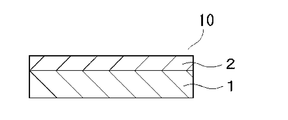
- FIG. 1 is a schematic cross-sectional view showing a preferred embodiment of an adhesive sheet for processing a semiconductor wafer of the present invention, in which a base resin film 1 and an adhesive layer 2 are formed on the base resin film 1.
- FIG. 2 is a schematic sectional view showing another preferred embodiment of the pressure-sensitive adhesive sheet for processing semiconductor wafers of the present invention.
- the adhesive layer 2 is formed on the base resin film 1, the base resin film 1, and the adhesive layer 3 is further formed.
- the pressure-sensitive adhesive layer in the present invention is composed of a radiation curable resin composition in which a specific photopolymerization initiator is contained in a specific blending amount together with a specific blending amount of a radiation polymerizable compound in a base resin.
- the pressure-sensitive adhesive sheet for processing a semiconductor wafer in which an adhesive layer is formed on the pressure-sensitive adhesive layer is also irradiated with radiation from the side of the below-described radiation-transmissive base resin film, and the pressure-sensitive adhesive layer Reduce the adhesive strength.
- the pressure-sensitive adhesive layer Reduces the adhesive strength.
- the adhesive sheet for semiconductor wafer processing of the present invention shown in FIG. 1 can be peeled off without any problems in the pick-up process after radiation irradiation even when it is bonded to the back surface immediately after finishing the back surface grinding of the semiconductor wafer.
- the surface of the semiconductor wafer immediately after the end of the grinding is an active surface in which a natural oxide film is not entirely formed and active atoms in an unoxidized state are present.
- the pressure-sensitive adhesive sheet for processing a semiconductor wafer of the present invention can be peeled off without any problem after irradiation, and the adhesion of contaminants due to the pressure-sensitive adhesive component can be remarkably reduced.
- the pressure-sensitive adhesive sheet for processing a semiconductor wafer according to the present invention in which an adhesive layer is further provided on the pressure-sensitive adhesive layer, is shown in FIG. 2 by the heat generated by radiation irradiation after the dicing process is completed. There is no problem in peeling off.
- the pressure-sensitive adhesive layer is formed by using a radiation curable resin composition on a base resin film described later.
- the semiconductor wafer processing sheet of the present invention includes the first aspect and the second aspect. Each mode includes the mode shown in FIG. 1 and the semiconductor wafer processing sheet shown in FIG.
- the base resin of the pressure-sensitive adhesive layer of the semiconductor wafer processing sheet of the first embodiment is (i-1) a (meth) acrylic group having a radiation-curable carbon-carbon double bond-containing group with respect to the repeating unit of the main chain.
- the main component is an acrylic polymer (a) bonded with a residue having a monomer part.
- the base resin of the radiation curable resin composition used for the pressure-sensitive adhesive layer of the semiconductor wafer processing sheet of the first aspect has a radiation curable carbon-carbon double bond-containing group with respect to the repeating unit of the main chain
- the polymer is mainly composed of a polymer (a) bonded with a residue having a (meth) acrylic monomer portion.
- the polymer (a) as a main component means that the content in the base resin is 50 to 100% by mass.
- the (meth) acrylic monomer includes both an acrylic monomer and a methacrylic monomer.
- the polymer (a) may be produced by any method.
- the polymer (a) includes an acrylic copolymer and / or a methacrylic copolymer having a radiation curable carbon-carbon double bond with respect to a repeating unit of the main chain and having a functional group.
- the thing obtained by making (a1) and the compound (a2) which has a functional group which can react with this functional group react is mentioned.
- an acrylic copolymer and / or a methacrylic copolymer having a functional group is defined as (a1 ′), which has a radiation-curable carbon-carbon double bond and can react with the functional group of (a1 ′).
- a compound having a group may be (a2 ′), and these may be reacted to obtain a polymer (a).
- the acrylic copolymer and / or methacrylic copolymer (a1) having a radiation curable carbon-carbon double bond and a functional group with respect to the repeating unit of the main chain is, for example, radiation curing.
- a monomer (a1-1) such as an alkyl acrylate and / or alkyl methacrylate having a functional carbon-carbon double bond and a monomer (a1-2) having a functional group are copolymerized. Obtainable.
- a (meth) acrylic acid alkyl ester having 6 to 12 carbon atoms in the alkyl group of the alkyl ester eg, hexyl acrylate, n-octyl acrylate, isooctyl acrylate, 2- Ethyl hexyl acrylate, dodecyl acrylate, decyl acrylate.
- (meth) acrylic acid alkyl ester having 5 or less carbon atoms in the alkyl group of the alkyl ester (for example, pentyl acrylate, n-butyl acrylate, isobutyl acrylate, ethyl acrylate, methyl acrylate, or similar methacrylates) Can be mentioned.
- the glass transition point tends to decrease as the alkyl ester of the alkyl ester having a larger number of carbon atoms (meth) acrylic acid alkyl ester is used. Therefore, the polymer (a) having a desired glass transition point can be obtained by appropriately selecting the carbon number of the alkyl group of the alkyl ester of the monomer (a1-1).
- a low molecular compound having a carbon-carbon double bond such as vinyl acetate, styrene or acrylonitrile is added to (a1-1) for the purpose of improving compatibility with other components and various performances.
- a polymer (a) can be obtained.
- the blending amount of these low molecular compounds is preferably 5% by mass or less of the monomer (a1-1).
- Examples of the functional group possessed by the monomer (a1-2) include a carboxyl group, a hydroxyl group, an amino group, a cyclic acid anhydride group, an epoxy group, and an isocyanate group.
- Specific examples of the monomer (a1-2) include, for example, acrylic acid, methacrylic acid, cinnamic acid, itaconic acid, fumaric acid, phthalic acid, 2-hydroxyalkyl acrylates, 2-hydroxyalkyl methacrylates, glycol Monoacrylates, glycol monomethacrylates, N-methylolacrylamide, N-methylolmethacrylamide, allyl alcohol, N-alkylaminoethyl acrylates, N-alkylaminoethyl methacrylates, acrylamides, methacrylamides, maleic anhydride, Some of the isocyanate groups of itaconic anhydride, fumaric anhydride, phthalic anhydride, glycidyl acrylate, g
- examples of the functional group (a1) include a hydroxyl group, an epoxy group, and an isocyanate group.
- examples of the functional group (a2) include a hydroxyl group, an epoxy group, and an isocyanate group.
- examples of the functional group (a1) include a cyclic acid anhydride group and an isocyanate group.
- examples of the functional group (a2) include an amino group, examples of the functional group (a1) include an epoxy group and an isocyanate group.
- examples of the functional group of (a2) include a carboxyl group, a cyclic acid anhydride group, and an amino group.
- those similar to those listed in the specific examples of the monomer (a1-2) can be listed.
- the acid value or the hydroxyl value can be suitably set within a range as described later.
- the polymer (a) containing as a constituent unit a (meth) acrylic monomer having a radiation-curable carbon-carbon double bond-containing group with respect to the repeating unit of the main chain can be solution-polymerized in various solvents. Can be obtained.
- a ketone, ester, alcohol, or aromatic solvent can be used as the organic solvent in the case of solution polymerization. In general, it is preferable to use a good solvent for an acrylic polymer and a solvent having a boiling point of 60 to 120 ° C.
- toluene, ethyl acetate, isopropyl alcohol, benzene, methyl cellosolve, ethyl cellosolve, acetone, methyl ethyl ketone, and the like can be used.
- radical generators such as azobis compounds such as ⁇ , ⁇ ′-azobisisobutylnitrile and organic peroxide compounds such as benzoyl peroxide can be used.
- a catalyst and a polymerization inhibitor can be used in combination, and the polymer (a) having a desired molecular weight can be obtained by adjusting the polymerization temperature and the polymerization time.
- a mercaptan or carbon tetrachloride solvent it is preferable to use a mercaptan or carbon tetrachloride solvent.
- the synthesis of the polymer (a) is not limited to solution polymerization, and other methods such as bulk polymerization and suspension polymerization may be used.
- the weight average molecular weight of the polymer (a) in which a residue having a (meth) acrylic monomer part having a radiation-curable carbon-carbon double bond-containing group is bonded to a repeating unit of the main chain Is preferably about 300,000 to 1,000,000. If it is less than 300,000, the cohesive force due to radiation irradiation becomes small, and when the wafer is diced, the device is likely to be displaced, and image recognition may be difficult. In order to prevent the deviation of the element as much as possible, the molecular weight is preferably 400,000 or more. Further, if the molecular weight exceeds 1,000,000, there is a possibility of gelation at the time of synthesis and coating.
- the weight average molecular weight of the polymer (a) in the present invention can be determined, for example, as a weight average molecular weight in terms of polystyrene by the following method.
- GPC device HLC-8120GPC (trade name, manufactured by Tosoh Corporation)
- Column TSK gel SuperHM-H / H4000 / H3000 / H2000 (trade name, manufactured by Tosoh Corporation)
- Flow rate 0.6 ml / min
- Concentration 0.3% by mass Injection volume: 20 ⁇ l
- Developing solvent Chloroform
- the iodine value of the polymer (a) containing an acrylic monomer having a radiation-polymerizable carbon-carbon double bond-containing group with respect to the main chain as a structural unit is 1 to 50. More preferably, it is 2 to 30, and if it is less than 1, the degree of cross-linking after radiation irradiation is so small that the peeling force cannot be lowered, so that the chip cannot be sufficiently picked up. If it exceeds 50, the degree of cross-linking after irradiation is high and curing shrinkage occurs, and the pick-up property of the chip decreases.
- the acid value of the polymer (a) is preferably 0.5 to 30.
- the hydroxyl value and the acid value are values measured by JIS K 0070.
- the base resin used in the radiation curable resin composition constituting the pressure-sensitive adhesive layer of the present invention may be blended with conventional ones within a range that does not impair the gist of the present invention.
- natural rubber, rubber-based polymers such as various synthetic rubbers, or poly (meth) acrylic acid alkyl ester, (meth) acrylic acid alkyl ester, (meth) acrylic acid alkyl ester and other non-polymerizable copolymers thereof.
- Acrylic copolymers such as copolymers with saturated monomers can be used.
- the base resin of the radiation curable resin composition used for the adhesive layer of the semiconductor wafer processing sheet according to the second aspect is an acrylic polymer.
- a (meth) acrylic acid ester component is a monomer main component (mass% in the polymer exceeds 50%), and the (meth) acrylic acid ester component can be copolymerized. Examples include those obtained by copolymerization with monomer components.
- examples of the (meth) acrylic acid ester component as the main monomer component include methyl (meth) acrylate, ethyl (meth) acrylate, propyl (meth) acrylate, and isopropyl (meth) acrylate.
- a polyisocyanate compound In the radiation-curable resin composition constituting the pressure-sensitive adhesive layer of the pressure-sensitive adhesive sheet for semiconductor wafer processing according to the first aspect and the second aspect, a polyisocyanate compound, an alkyl etherified melamine compound, an epoxy compound, and a silane cup Conventional curing agents such as ring agents can be included. By setting it as the resin composition which mix
- isocyanate curing agent examples include polyvalent isocyanate compounds such as 2,4-tolylene diisocyanate, 2,6-tolylene diisocyanate, 1,3-xylylene diisocyanate, 1,4-xylene diisocyanate, diphenylmethane.
- the radiation curable resin composition used for the pressure-sensitive adhesive layer of the semiconductor wafer processing sheet according to the second aspect has a weight average molecular weight of 10,000 or less having at least two photopolymerizable carbon-carbon double bonds in the molecule.
- the compound (c) is contained.
- the compound (c) can be used without particular limitation as long as it can be cured by irradiation with radiation to form a three-dimensional network.
- This compound includes an oligomer having a weight average molecular weight of 10,000 or less and does not include a high molecular weight polymer having a weight average molecular weight exceeding 10,000.
- the molecular weight is 5,000 or less and the number of radiation-polymerizable carbon-carbon double bonds in the molecule is 2 to 6 so that the three-dimensional network of the pressure-sensitive adhesive layer can be efficiently formed by irradiation with radiation. Those are preferred.
- the weight average molecular weight of the low molecular weight compound having at least two photopolymerizable carbon-carbon double bonds in the molecule is the polystyrene equivalent measured by GPC (gel permeation chromatography) under the following conditions. It refers to the weight average molecular weight.
- GPC device HLC-8120GPC (trade name, manufactured by Tosoh Corporation)
- Examples of the radiation polymerizable compound (c) include trimethylolpropane triacrylate, tetramethylolmethane tetraacrylate, pentaerythritol triacrylate, pentaerythritol tetraacrylate, dipentaerythritol monohydroxypentaacrylate, dipentaerythritol hexaacrylate, 1, Examples include 4-butylene glycol diacrylate, 1,6-hexanediol diacrylate, polyethylene glycol diacrylate, organopolysiloxane composition, commercially available oligoester acrylate, and urethane acrylate.
- a compound having at least two photopolymerizable carbon-carbon double bonds in the molecule and having a weight average molecular weight of 10,000 or less may be used alone or in combination of two or more.
- the blending amount is 1 to 300 parts by mass with respect to 100 parts by mass of the base resin.
- the amount is 30 to 200 parts by mass, and more preferably 50 to 150 parts by mass with respect to 100 parts by mass of the base resin. If the amount is too small, three-dimensional reticulation by irradiation of the pressure-sensitive adhesive layer becomes insufficient, the semiconductor wafer processing pressure-sensitive adhesive sheet becomes difficult to peel from the wafer, and the wafer may be contaminated.
- photopolymerization initiator In the radiation curable resin composition constituting the pressure-sensitive adhesive layer of the semiconductor wafer processing pressure-sensitive adhesive sheet of the first aspect and the second aspect, polystyrene is standardized by a gel permeation chromatography (hereinafter referred to as “GPC”) method.
- GPC gel permeation chromatography
- a photopolymerization initiator having a weight average molecular weight converted to a substance of less than 1000 is used.
- the weight average molecular weight of the photopolymerization initiator refers to a value measured by GPC under the following conditions.
- GPC device LCVP series manufactured by Shimadzu Corporation
- OligoPore 300 ⁇ 7.5 (trade name) (trade name, manufactured by Polymer Laboratories)
- Flow rate 1 ml / min
- Concentration 1 mg / ml
- Injection volume 50 ⁇ l
- Column temperature 40 ° C
- Developing solvent Chloroform
- the photopolymerization initiator generates radicals when irradiated with radiation such as light or ultraviolet rays.
- the curing reaction is promoted or the curing reaction of a compound having at least two photopolymerizable carbon-carbon double bonds in the molecule contained in the pressure-sensitive adhesive layer and having a weight average molecular weight of 10,000 or less is promoted.
- the upper limit of the weight average molecular weight by GPC in terms of polystyrene of the photopolymerization initiator is preferably 800, more preferably 600.
- the lower limit of the weight average molecular weight by GPC in terms of polystyrene of the photopolymerization initiator is not particularly limited, but is preferably 200 or more.
- the molecular weight is small, it becomes easy to sublimate, and the shift from the pressure-sensitive adhesive layer to the non-adherent layer becomes remarkable, so that the wafer is easily contaminated.
- the heat resistance of the pressure-sensitive adhesive layer is deteriorated, and the pressure-sensitive adhesive layer is easily decomposed in the drying step after the base material is coated during production. Therefore, a stable curing reaction may not be exhibited.
- photopolymerization initiator examples include benzophenone, 4,4-bis (diethylamino) benzophenone, 2,4,6-trimethylbenzophene, 4-phenylbenzophenone, t-butylanthraquinone, 2-ethylanthraquinone, diethoxyacetophenone, 2-hydroxy-2-methyl-1-phenylpropan-1-one, 2,2-dimethoxy-1,2-diphenylethane-1-one, 1-hydroxycyclohexyl-phenyl ketone, benzoin methyl ether, benzoin ethyl ether, Benzoin isopropyl ether, benzoin isobutyl ether, 2-methyl-1- [4- (methylthio) phenyl] -2-morpholinopropan-1-one, 2-benzyl-2-dimethylamino-1- (4-morpholinophenyl) -Butano -1, diethylthioxanthone, isopropyl
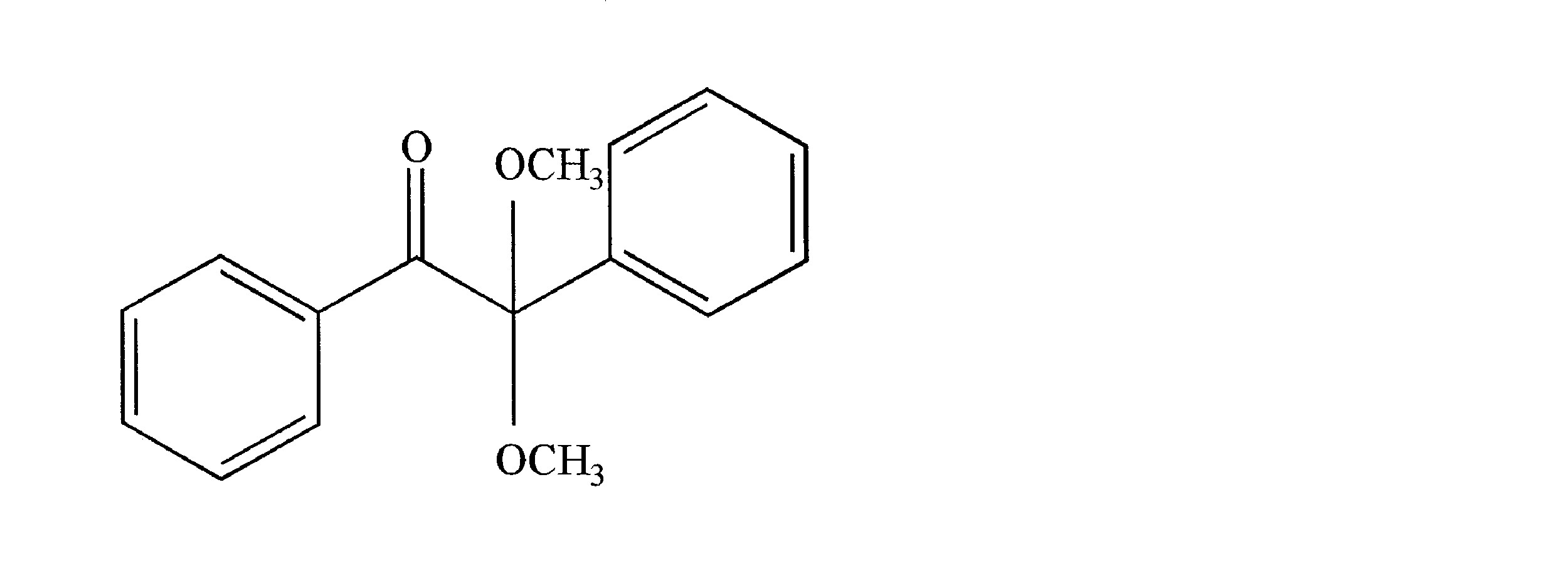
- 2,2-dimethoxy-1,2-diphenylethane-1-one (molecular weight 260), 2 is an excellent photopolymerization initiator that hardly sublimes and hardly generates a residue of contamination.
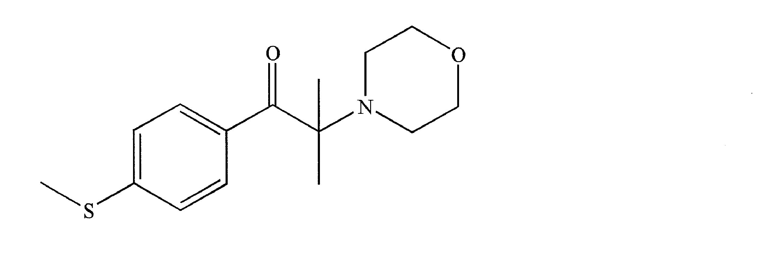
- -Methyl-1- (4-methylthiophenyl) -2-morpholinopropan-1-one (molecular weight 280), 1-hydroxy-cyclohexylphenyl-ketone (molecular weight 205).
- the photopolymerization initiator is blended in an amount of 0.1 to 10 parts by mass with respect to 100 parts by mass of the base resin in the radiation curable resin composition constituting the pressure-sensitive adhesive layer of the semiconductor wafer processing pressure-sensitive adhesive sheet of the first aspect.
- 1 to 10 parts by mass is blended with respect to 100 parts by mass of the base resin, and more preferably 2 to 7 parts by mass.
- 0.1 to 10 parts by mass is blended with 100 parts by mass of the acrylic polymer.
- 1 to 10 parts by mass is blended with 100 parts by mass of the acrylic polymer, and more preferably 2 to 7 parts by mass.
- the pressure-sensitive adhesive layer is not sufficiently three-dimensionally formed by irradiation with radiation, and cannot be peeled off from the adhesive layer well, or the semiconductor chip is contaminated. Moreover, when there are too many photoinitiators, the effect corresponding to it may not be acquired, but there exists a possibility that this photoinitiator may remain on a wafer. If necessary, two or more of the above photopolymerization initiators may be used in combination.
- the weight average molecular weight by each GPC of the photoinitiator used should just be less than 1000.
- amine compounds such as triethylamine, tetraethylpentamine, dimethylaminoethanol, and thioxanthone photopolymerization initiators can be used in combination as photopolymerization accelerators.
- the radiation curable resin composition may contain a tackifier, a tackifier, a surfactant, other modifiers and conventional components as necessary to adjust the adhesion to the semiconductor wafer.
- a tackifier a tackifier
- surfactant other modifiers and conventional components as necessary to adjust the adhesion to the semiconductor wafer.
- surfactants and compounds showing surface activity may contaminate the semiconductor wafer, it is preferable to use as few as possible.
- the above base resin a compound having at least two photopolymerizable carbon-carbon double bonds in the molecule and a weight average molecular weight of 10,000 or less, specific photopolymerization initiation
- a radiation-polymerizable resin composition containing an agent, and if necessary, a crosslinking agent and other compounding ingredients is directly applied and dried by heating, or once applied to release paper and dried, and then transferred onto a base resin film.
- the adhesive sheet for semiconductor wafer processing by which the adhesive layer was comprised by the layer using a radiation polymerizable resin composition can be manufactured.
- the pressure-sensitive adhesive layer is formed so that the thickness of the pressure-sensitive adhesive layer is usually 5 to 100 ⁇ m to obtain a pressure-sensitive adhesive sheet for processing semiconductor wafers such as sheets and tapes.
- the radiation alpha rays, gamma rays, electron beams, ultraviolet rays, and the like can be used, and there is no particular limitation as long as the adhesive strength can be reduced by curing the adhesive layer. Electron beams and ultraviolet rays are preferred, and ultraviolet rays are more preferred when a photopolymerization initiator is used.
- a pressure-sensitive adhesive layer 2 may be provided on a base resin film 1, and an adhesive layer 3 may be further formed thereon.
- the method for forming the pressure-sensitive adhesive layer and then the adhesive layer on the base resin film is not particularly limited.
- the pressure-sensitive adhesive layer is laminated on the base resin film, and further the adhesive on the pressure-sensitive adhesive layer. What is necessary is just to laminate
- the adhesive sheet for semiconductor wafer processing is bonded to the back surface of the semiconductor wafer after grinding, and then the adhesive and the adhesive are simultaneously cut by dicing from the circuit forming surface side of the semiconductor wafer. And a semiconductor chip with an adhesive layer can be obtained.
- the adhesive used for the adhesive layer 3 a conventional adhesive can be used.
- an adhesive layer formed in advance can be used.
- conventional polyimide resin, polyamide resin, polyetherimide resin, polyamideimide resin, polyester resin, polyesterimide resin, phenoxy resin, polysulfone resin, polyethersulfone resin, polyphenylene sulfide resin, polyether ketone used for adhesives Resins, chlorinated polypropylene resins, acrylic resins, polyurethane resins, epoxy resins, polyacrylamide resins, melamine resins, and the like, and mixtures thereof can be used.
- an epoxy resin in terms of good heat resistance after curing. Any epoxy resin that cures and exhibits an adhesive action may be used.
- a polyfunctional epoxy resin may be added.
- the polyfunctional epoxy resin include phenol novolac type epoxy resins and cresol novolac type epoxy resins.
- the epoxy resin curing agent is not particularly limited as long as it is usually used as a curing agent.
- One molecule of amine compound, polyamide, acid anhydride, polysulfide, boron trifluoride, phenolic hydroxyl group is used. Examples thereof include bisphenol A, bisphenol F, and bisphenol S, which are compounds having two or more compounds.
- phenol novolac resin bisphenol novolac resin, or the like, which is a phenol resin, because of its excellent resistance to electric corrosion during moisture absorption.
- a curing accelerator together with the curing agent in terms of shortening the heat treatment time for curing.
- bases such as various imidazoles such as 2-methylimidazole, 2-ethyl-4-methylimidazole, 1-cyanoethyl-2-phenylimidazole, 1-cyanoethyl-2-phenylimidazolium trimellitate are used. it can.
- a silane coupling agent or a titanium coupling agent as an additive to the resin or a mixture thereof in order to enhance the adhesion to the semiconductor chip or the lead frame.
- a filler may be added for the purpose of improving heat resistance and adjusting fluidity.
- a filler for example, silica, alumina, antimony oxide, and the like can be used. These fillers can be used by mixing at an arbitrary ratio as long as the maximum particle size is smaller than the thickness of the adhesive layer.
- the thickness of the adhesive layer is not particularly limited, but is usually preferably about 5 to 100 ⁇ m. Moreover, you may laminate
- the pressure-sensitive adhesive layer is bonded to the ring frame, and usually the adhesive layer that is difficult to peel off from the adherend is not bonded, so the pressure-sensitive adhesive sheet for semiconductor wafer processing of the present invention is used after use It can be easily peeled from the ring frame.
- the adhesive sheet for processing a semiconductor wafer of the present invention requires that the base resin film be radiation transparent in order to cure the adhesive layer by irradiating radiation from the base resin film side at the time of peeling. Further, when processing a wafer, it receives an impact by a cutting blade or the like and receives a pressure from cleaning water or the like. For this reason, a base resin film has the intensity
- the surface of the base resin film on which the pressure-sensitive adhesive layer is formed is preferably subjected to various surface treatments including corona treatment in order to make the pressure-sensitive adhesive layer difficult to peel from the base resin film.
- Materials used for the base resin film include polyethylene, polypropylene, ethylene-propylene copolymer, polyvinyl chloride, polyethylene terephthalate, polybutylene terephthalate, ethylene-vinyl acetate copolymer, polybutene-1 And films of poly-4-methylpentene-1, ethylene-ethyl acrylate copolymer, ethylene-methyl acrylate copolymer, ethylene-acrylic acid copolymer, polyurethane, polymethylpentene, polybutadiene and the like. it can.
- the thickness of the base resin film is 30 to 500 ⁇ m, preferably 40 to 300 ⁇ m, more preferably 50 to 200 ⁇ m.
- the strength will be weakened, which may cause problems due to breakage or the like during semiconductor wafer processing.
- the base resin film is too thick, the semiconductor wafer processing pressure-sensitive adhesive sheet is too hard in the pick-up process of the semiconductor chip after the dicing process is completed, which causes a problem in pushing up with the needle.
- the dicing process is completed, and it becomes difficult to sufficiently stretch the semiconductor wafer processing pressure-sensitive adhesive sheet in the expanding process before the pickup process. For this reason, the gap between the semiconductor chips is small, the chip recognizability by the image is insufficient, and the pickup failure of the semiconductor chip occurs.
- the iodine value of the polymer (a1) used in Examples 1-1 to 1-9 and 1-11 and Comparative Examples 1-1 to 1-4 and 1-7 is It was 20.
- the iodine value of the polymer (a2) used in Example 1-10 was 50
- the iodine value of the polymer (a3) used in Example 1-12 was 0.5
- the weight used in Example 1-13 was The iodine value of combined (a4) was 55.
- the polymer ((a1) to (a4)) will be described as the polymer (a).
- GPC device HLC-8120GPC (trade name, manufactured by Tosoh Corporation) Column: TSK gel SuperHM-H / H4000 / H3000 / H2000 (trade name, manufactured by Tosoh Corporation) Flow rate: 0.6 ml / min, Concentration: 0.3% by mass Injection volume: 20 ⁇ l, Column temperature: 40 ° C Developing solvent: Chloroform (ii) Glass transition temperature Differential scanning calorimeter (DSC) (DSC7020 (trade name), manufactured by Seiko Instruments Inc.), using a differential scanning calorimeter (DSC), the rate of temperature increase is 5 Measured at ° C / min. (Iii) Double bond amount Iodine value was determined according to JIS K 0070.
- the weight average molecular weight of the photoinitiator was measured by the GPC method, and the weight average molecular weight was calculated using polystyrene as a standard substance. The results are also shown in Tables 1-1 to 1-4. As gel permeation chromatography, OligoPore 300 ⁇ 7.5 (trade name) manufactured by Polymer Laboratories was used. The developing solvent was chloroform, and the measurement was performed at 40 ° C.
- UN-3320HA (trade name, manufactured by Negami Kogyo): 1500 (double bond amount: 6) UN-3320HC (trade name, manufactured by Negami Kogyo): 1500 (double bond amount: 6) UN-9000PEP (trade name, manufactured by Negami Kogyo): 5000 (double bond amount: 2) UN-6050PTM (trade name, manufactured by Negami Kogyo): 6000 (double bond amount: 2) UN-901T (trade name, manufactured by Negami Kogyo): 4000 (double bond amount: 9) UN-9200A (trade name, manufactured by Negami Kogyo): 11500 (double bond amount: 2) (Measurement conditions for weight average molecular weight)
- GPC device HLC-8120GPC (trade name, manufactured by Tosoh Corporation) Column: TSK-GEL G2500HHR (trade name, manufactured by Tosoh Corporation) Flow rate: 1 ml / min Concentration: 0.2 mg / ml Injection volume: 100 ⁇ l, Ther
- VPE-0201 (trade name, manufactured by Wako Pure Chemical Industries, Ltd.) was used as the polyethylene glycol unit-containing polymer azo polymerization initiator.
- the weight average molecular weight of the photoinitiator was measured by a gel permeation chromatography (GPC) method, and the weight average molecular weight was calculated using polystyrene as a standard substance. The results are also shown in Tables 2-1 to 2-4.
- GPC gel permeation chromatography
- OligoPore 300 ⁇ 7.5 (trade name) manufactured by Polymer Laboratories was used.
- the developing solvent was chloroform, and the measurement was performed at 40 ° C.
- a base resin film having a thickness of 100 ⁇ m was produced by T-die method using EMMA resin (trade name, trade name: ACRIFT WD201 manufactured by Sumitomo Chemical Co., Ltd.).
- EMMA resin trade name, trade name: ACRIFT WD201 manufactured by Sumitomo Chemical Co., Ltd.
- Examples 1-1 to 1-10, 1-12 to 1-13, 2-1 to 2-10, Comparative Examples 1-1 to 1-4, 2-1 to 2-5 The radiation curable resin composition shown in 1 was applied and cured appropriately. Thereby, the adhesive sheet for semiconductor wafer processing of the structure shown in FIG. 1 which has an adhesive layer whose film thickness after drying is 10 micrometers was obtained.
- This pressure-sensitive adhesive layer and the adhesive layer of the adhesive sheet produced by the method described above are laminated and laminated, and a pressure-sensitive adhesive sheet in which a release film is laminated on a semiconductor wafer processing pressure-sensitive adhesive sheet having the configuration shown in FIG. 2-11 to 2-15 and Comparative Examples 2-6 and 2-7).
- the release film was peeled off and bonded to a semiconductor wafer for evaluation.
- Performance test Dicing was performed under the following conditions, and then the pickup property and chip contamination were evaluated.
- (Dicing conditions) (1) Adhesive sheets for processing semiconductor wafers having the structure shown in FIG. 1 Examples 1-1 to 1-10, 1-12, 1-13, 2-1 to 2-10, Comparative Examples 1-1 to 1-4, Regarding 2-1 to 2-5, using “DFD-840” manufactured by DISCO, the back surface of the silicon wafer was ground by 30 ⁇ m with two axes, and then ground so that the final thickness of the silicon wafer was 100 ⁇ m. The grinding conditions at that time were as follows.
- the adhesive sheet for semiconductor wafer processing having the configuration shown in FIG. 1 is adhered and fixed to an 8-inch ring frame, and the adhesive sheet for semiconductor wafer processing is attached to the adhesive sheet for semiconductor wafer processing.
- Inch silicon wafers were bonded and full-cut dicing was performed to a chip size of 5 mm ⁇ 5 mm using a dicing apparatus DAD340 (trade name) manufactured by DISCO.
- the cutting depth of the blade from the adhesive sheet surface for processing a semiconductor wafer was 30 ⁇ m in the case of the adhesive sheet having the configuration shown in FIG.
- Adhesive sheet for processing semiconductor wafers having the structure shown in FIG. 2 For Examples 1-11 and 2-11 to 2-15 and Comparative Examples 1-7, 2-6, and 2-7, 8 inch silicon having a thickness of 100 ⁇ m
- a semiconductor wafer processing pressure-sensitive adhesive sheet having the configuration shown in FIG. 2 was bonded to the wafer at 70 ° C. for 20 seconds, and then diced using DFD 6340 manufactured by Disco Corporation under the following conditions.
- Dicing blade (thin rotary grindstone): 1st Disco 27HEEE 2nd Disco 27HEDD Blade rotation speed: 35000rpm Blade feed rate: 50mm / s Chip size: 5mm x 5mm Cutting depth: First time 50 ⁇ m to silicon wafer 2nd time 40 ⁇ m to semiconductor wafer processing adhesive sheet (base resin film thickness 100 ⁇ m, adhesive layer thickness 10 ⁇ m, adhesive layer thickness 20 ⁇ m)
- Chip fouling property is as shown in FIG. 1 for semiconductor wafer processing adhesive sheets (Examples 1-1 to 1-10, 1-12, 1-13, 2-1 to 2-10, comparative examples) 1-1 to 1-4 and 2-1 to 2-5) were evaluated by the following methods.
- (2) -1 Visual test When the above chipping property was evaluated, the chip was peeled off and visually confirmed. The case where there is no rainbow-colored gloss due to adhesion of adhesive or contamination on the back of the wafer is accepted. The case where it does is rejected, and it displayed by x.
- (2) -2 Foreign matter test A semiconductor wafer processing adhesive sheet was bonded to a mirror-finished silicon wafer (6 inches) whose surface was cleaned, and the sheet was peeled off after being left for 24 hours.
- the number of foreign matters remaining on the wafer surface to which the sheet was bonded was measured with a laser surface inspection device (Surf Scan 6420 (trade name, manufactured by KLA Tencor Co., Ltd.). Of these, ⁇ and ⁇ were accepted, ⁇ was considered as a practically acceptable level, and x was rejected, and the results are shown in the table. ⁇ : Less than 20, ⁇ : 20 or more and less than 90, ⁇ : 90 or more and less than 200, ⁇ : 200 or more
- UV irradiation was performed from the substrate resin film surface side of the semiconductor wafer processing pressure-sensitive adhesive sheet so that the irradiation amount was 200 mJ / cm 2 .
- the peeling force of the semiconductor wafer processing pressure-sensitive adhesive sheet on the silicon wafer after ultraviolet irradiation was measured.
- the measurement conditions were 90 ° peeling and peeling speed of 50 mm / min). The case where the peeling force was 0.5 N / 25 mm or less was determined to be acceptable, and the result was ⁇ .
- Example 1-11 which was evaluated for the semiconductor wafer processing pressure-sensitive adhesive sheet having the structure shown in FIG. 2, interfacial delamination was successfully achieved between the pressure-sensitive adhesive layer and the adhesive layer. , All the semiconductor chips out of 200 chips could be picked up. On the other hand, in Comparative Example 1-7, the interface peeling between the pressure-sensitive adhesive layer and the adhesive layer was not successful, and only 100 semiconductor chips out of 200 chips could be picked up.
- Comparative Example 2-7 using a compound having at least two photopolymerizable carbon-carbon double bonds in the molecule and having a weight average molecular weight of 11,500, as in Comparative Example 2-6, Of the chips, only 100 semiconductor chips could be picked up.
Landscapes
- Chemical & Material Sciences (AREA)
- Organic Chemistry (AREA)
- Chemical Kinetics & Catalysis (AREA)
- Adhesives Or Adhesive Processes (AREA)
- Dicing (AREA)
- Adhesive Tapes (AREA)
Abstract
Description
(1)高純度シリコン単結晶をスライスして半導体ウエハとした後、該ウエハ表面にICなどの所定の回路パターンを形成する。
(2)半導体ウエハ回路面を保護する表面保護テープを貼合して、形成された回路面を保護した上で、該ウエハ裏面を研削機により研削して、ウエハの厚さを100~600μm程度まで薄くし、その後表面保護テープを回路面から剥離する。
(3)半導体ウエハの直径よりもやや大きな中空部分を有する輪状のダイシングフレームにダイシングシートを貼合し、該フレームの中空部分に露出した粘着剤層に前記研削機で研削されたウエハ裏面を貼合する。
(4)ダイシングシートが貼合された面とは反対側(すなわち、回路が形成された側)からダイシングして半導体チップとし、紫外線などの放射線を照射してダイシングシートの粘着剤層の粘着力を低下させて、該チップをダイシングシートの基材フィルム側からニードルで突き上げてピックアップを行う。
一方、近年、直径300mmの大口径のウエハから厚さ100μm以下の薄型の半導体チップを得ることが主流となっている。そこでこの薄型ウエハからいかに問題なく半導体チップを得ることが重要な課題である。
しかし、従来の粘着剤層を有するダイシングシートでは、ウエハ裏面に酸化被膜が生成した後に貼合されていたので、この場合にはうまく剥離できたものでも、同様にインライン製造装置で使用してもうまく剥離できないという問題が生じることとなった。
また、従来の製造工程では、ダイシングシートをウエハ裏面に酸化被膜が生成した後に貼合されていたので、この場合にはうまく剥離できた従来の粘着剤層を有するダイシングシートをインライン製造装置で同様に使用してもうまく剥離できないという問題が生じることとなった。
また本発明は、粘着剤層上にさらに接着剤層が設けられた半導体ウエハ加工用粘着シートにより、接着剤層と粘着剤層とをピックアップ工程で容易に剥離して、接着剤層付きの半導体チップを得ることができる半導体ウエハ加工用粘着シートを提供することを課題とする。
すなわち、本発明は、
<1>放射線透過性の基材樹脂フィルムと、該基材樹脂フィルム上に粘着剤層が形成された半導体ウエハ加工用粘着シートであって、該粘着剤層が
(i-1)主鎖の繰り返し単位に対して放射線硬化性炭素-炭素二重結合含有基を有する(メタ)アクリル系単量体部を有する残基を結合したアクリル系重合体(a)を主成分とするベース樹脂100質量部に対し、
(iii)ゲル透過クロマトグラフィ(以下、「GPC」という)法によって、ポリスチレンを標準物質として換算された重量平均分子量が1000未満の光重合開始剤(b)0.1~10質量部
を含有する放射線硬化性樹脂組成物を用いた層で構成されていることを特徴とする半導体ウエハ加工用粘着シート、
<2>放射線透過性の基材樹脂フィルムと、該基材樹脂フィルム上に粘着剤層が形成された半導体ウエハ加工用粘着シートであって、該粘着剤層が
(i-2)アクリル系重合体100質量部に対し、
(ii) 分子内に光重合性炭素-炭素二重結合を少なくとも2個有する重量平均分子量が10,000以下の化合物(c)1~300質量部、
(iii)ゲル透過クロマトグラフィ(以下、「GPC」という)法によって、ポリスチレンを標準物質として換算された重量平均分子量が1000未満の光重合開始剤(b)0.1~10質量部
を含有する放射線硬化性樹脂組成物を用いた層で構成されることを特徴とする半導体ウエハ加工用粘着シート、
<3>前記光重合開始剤(b)が、1-ヒドロキシ-シクロヘキシルフェニル-ケトン、2,2-ジメトキシ-1,2-ジフェニルエタン-1-オン、2-メチル-1-(4-メチルチオフェニル)-2-モルフォリノプロパン-1-オン、および下記一般式(1)で表されるオリゴマー
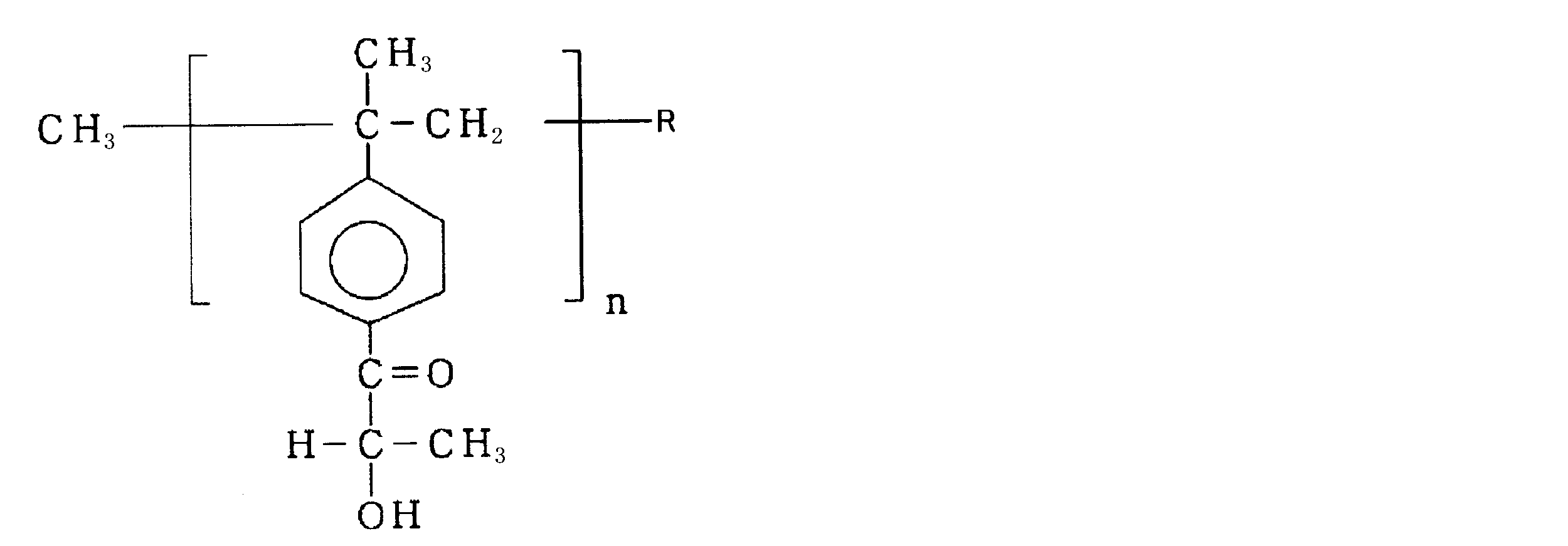
(式中、Rはアルキル基を表す。nは整数である。)
からなる群から選ばれる少なくとも1種であることを特徴とする<1>又は<2>記載の半導体ウエハ加工用粘着シート、
<4>前記一般式(1)で表されるオリゴマーの重合度がn=2~4であることを特徴とする<3>記載の半導体ウエハ加工用粘着シート、
<5>前記主鎖の繰り返し単位に対して放射線重合性炭素-炭素二重結合含有基を有するアクリル系単量体を構成単位として含む重合体(a)のヨウ素価が1~50であることを特徴とする<1>、<3>又は<4>記載の半導体ウエハ加工用粘着シート、及び
<6><1>~<5>のいずれか1項記載の半導体ウエハ加工用粘着シートの粘着剤層上に、さらに接着剤層が設けられたことを特徴とする半導体ウエハ加工用粘着シート、
を提供するものである。
また本発明の粘着剤層上にさらに接着剤層が設けられた半導体ウエハ加工用粘着シートにより、接着剤層と粘着剤層とをピックアップ工程で容易に剥離して、接着剤層付きの半導体チップを得ることができる。
図1は本発明の半導体ウエハ加工用粘着シートの好ましい一実施形態を示す概略断面図であり、基材樹脂フィルム1と、基材樹脂フィルム1上に粘着剤層2が形成されている。また図2は本発明の半導体ウエハ加工用粘着シートの好ましい他の一実施形態を示す概略断面図である。図2においては、基材樹脂フィルム1と、基材樹脂フィルム1上に粘着剤層2が形成され、さらに接着剤層3が形成されている。
また図2に示す、粘着剤層上にさらに接着剤層が設けられた本発明の半導体ウエハ加工用粘着シートは、ダイシング工程終了後の放射線照射で発生した熱により、粘着剤層と接着剤層との剥離に問題が生じるということがない。
第1の態様の半導体ウエハ加工用シートの粘着剤層に用いられる放射線硬化性樹脂組成物のベース樹脂は、主鎖の繰り返し単位に対して放射線硬化性炭素-炭素二重結合含有基を有する(メタ)アクリル系単量体部を有する残基を結合した重合体(a)を主成分とするものである。本発明において、重合体(a)を主成分とするとは、ベース樹脂中の含有割合が50~100質量%のものをいう。また本発明においては、(メタ)アクリル系単量体は、アクリル系単量体とメタクリル系単量体の両者を含むものとする。
前記重合体(a)はどのようにして製造されたものでもよい。例えば、前記重合体(a)としては、主鎖の繰り返し単位に対して放射線硬化性炭素-炭素二重結合を有し、かつ官能基を有するアクリル系共重合体及び/又はメタクリル系共重合体(a1)と、該官能基と反応し得る官能基をもつ化合物(a2)とを反応させて得たものを挙げることができる。また、官能基を有するアクリル系共重合体及び/又はメタクリル系共重合体を(a1’)とし、放射線硬化性炭素-炭素二重結合を有するとともに(a1’)の官能基と反応し得る官能基を有する化合物を(a2’)とし、これらを反応させて、重合体(a)とすることもできる。
前記の主鎖の繰り返し単位に対して放射線硬化性炭素-炭素二重結合を有し、かつ官能基を有するアクリル系共重合体及び/又はメタクリル系共重合体(a1)は、例えば、放射線硬化性炭素-炭素二重結合を有するアクリル酸アルキルエステル及び/又はメタクリル酸アルキルエステルなどの単量体(a1-1)と、官能基を有する単量体(a1-2)とを共重合させて得ることができる。
また、ガラス転移点の他、他の成分との相溶性や各種性能を上げる目的で酢酸ビニル、スチレン、アクリロニトリルなどの炭素-炭素二重結合をもつ低分子化合物を(a1-1)に加えて重合体(a)を得ることができる。これらの低分子化合物の配合量は、単量体(a1-1)の5質量%以下とすることが好ましい。
具体例としては、単量体(a1-2)の具体例で列挙したものと同様のものを列挙することができる。
主鎖の繰り返し単位に対して放射線硬化性炭素-炭素二重結合含有基を有する(メタ)アクリル系単量体を構成単位として含む重合体(a)は、各種の溶剤中で溶液重合することにより得ることができる。溶液重合で行う場合の有機溶剤としては、ケトン系、エステル系、アルコール系、芳香族系のものを使用することができる。一般にアクリル系重合体の良溶媒で、沸点60~120℃の溶剤を使用することが好ましい。例えば、トルエン、酢酸エチル、イソプロピルアルコール、ベンゼン、メチルセロソルブ、エチルセロソルブ、アセトン、メチルエチルケトンなどを使用することができる。重合開始剤としては、α,α’-アゾビスイソブチルニトリルなどのアゾビス系、ベンゾイルペルオキシドなどの有機過酸化物系などのラジカル発生剤を用いることができる。この際、必要に応じて触媒、重合禁止剤を併用することができ、重合温度および重合時間を調節することにより、所望の分子量の重合体(a)を得ることができる。また、分子量を調節することに関しては、メルカプタン、四塩化炭素系の溶剤を用いることが好ましい。なお、重合体(a)の合成は、溶液重合に限定されるものではなく、塊状重合、懸濁重合など別の方法でもさしつかえない。
(重量平均分子量の測定条件)
GPC装置:HLC-8120GPC(商品名、東ソー社製)
カラム:TSK gel SuperHM-H/H4000/H3000/H2000、(商品名、東ソー社製)
流量:0.6ml/min、
濃度:0.3質量%、
注入量:20μl、
カラム温度:40℃
展開溶媒:クロロホルム
ここで水酸基価は及び酸価はJIS K 0070により測定された値をいうものとする。重合体(a)の水酸基価を適切な範囲内とすることにより、放射線照射後の粘着剤層の流動性を適切な範囲内とすることができ、放射線照射後の粘着力を十分に低下させることができる。重合体(a)の酸価を適切な範囲内とすることにより、放射線照射後の粘着剤層の流動性を適切な範囲内とすることができ、テープ復元性を満足させることができる。
第2の態様の半導体ウエハ加工用シートの粘着剤層に用いられる放射線硬化性樹脂組成物のベース樹脂は、アクリル系重合体である。
アクリル系重合体としては、(メタ)アクリル酸エステル成分をモノマー主成分(重合体中の質量%が50%を越える)とし、該(メタ)アクリル酸エステル成分に対して、共重合が可能なモノマー成分とを共重合したものなどが挙げられる。
上記の第1の態様及び第2の態様の半導体ウエハ加工用粘着シートの粘着剤層を構成する放射線硬化性樹脂組成物中に、ポリイソシアネート化合物、アルキルエーテル化メラミン化合物、エポキシ系化合物、シランカップリング剤などの従来から使用されている硬化剤を含ませることができる。硬化剤を配合した樹脂組成物とすることにより、初期の粘着力を任意の値に設定することができる。硬化剤の中でもイソシアネート系硬化剤を使用することが好ましい。
イソシアネート系硬化剤としては、具体的には多価イソシアネート化合物、例えば、2,4-トリレンジイソシアネート、2,6-トリレンジイソシアネート、1,3-キシリレンジイソシアネート、1,4-キシレンジイソシアネート、ジフェニルメタン-4,4’-ジイソシアネート、ジフェニルメタン-2,4’-ジイソシアネート、3-メチルジフェニルメタンジイソシアネート、ヘキサメチレンジイソシアネート、イソホロンジイソシアネート、ジシクロヘキシルメタン-4,4’-ジイソシアネート、ジシクロヘキシルメタン-2,4’-ジイソシアネート、リジンイソシアネートなどが用いられる。
第2の態様の半導体ウエハ加工用シートの粘着剤層に用いられる放射線硬化性樹脂組成物は、分子内に光重合性炭素-炭素二重結合を少なくとも2個有する重量平均分子量が10,000以下の化合物(c)を含有する。該化合物(c)は、放射線の照射により硬化して三次元網状化するものであれば特に制限なく使用することができる。この化合物には、重量平均分子量が10,000以下のオリゴマーを含み、重量平均分子量が10,0000を越える高分子重合体を含まないものとする。放射線の照射による粘着剤層の三次元網状化が効率よくなされるように、分子量が5,000以下でかつ分子内の放射線重合性の炭素-炭素二重結合の数が2~6個であるものが好ましい。
なお、本発明における分子内に光重合性炭素-炭素二重結合を少なくとも2個有する低分子量化合物の重量平均分子量とは、下記条件のGPC(ゲルーパーミエーション クロマトグラフ)で測定されたポリスチレン換算の重量平均分子量のことをいう。
(重量平均分子量の測定条件)
GPC装置:HLC-8120GPC(商品名、東ソー社製)
カラム :TSK-GEL G2500HHR(商品名、東ソー社製)
流量 :1ml/min
濃度 :0.2mg/ml
注入量 :100μl、
恒温槽温度:40℃
移動相 :クロロホルム
第1の態様及び第2の態様の半導体ウエハ加工用粘着シートの粘着剤層を構成する放射線硬化性樹脂組成物中には、ゲル透過クロマトグラフィ(以下、「GPC」という)法によって、ポリスチレンを標準物質として換算された重量平均分子量が1000未満の光重合開始剤を用いる。本発明においては、光重合開始剤の重量平均分子量は、下記条件のGPCで測定された値をいうものとする。
(重量平均分子量の測定条件)
GPC装置:島津製作所製 LCVPシリーズ
カラム:OligoPore 300×7.5(商品名)(商品名、PolymerLaboratories製)
流量: 1 ml/min、
濃度: 1mg/ml、
注入量: 50μl、
カラム温度:40℃
展開溶媒:クロロホルム
その場合の現象について、図面を参照して説明すると、図1に示すように、基材樹脂フィルム1に粘着剤層2が形成された半導体ウエハ加工用粘着シート10の場合には、半導体チップのピックアップに支障が生じる。また図2に示すように、基材樹脂フィルム1に粘着剤層2が設けられ、さらに接着剤層3が形成された半導体ウエハ加工用粘着シート20の場合には、接着剤層3と粘着剤層2との剥離を円滑に行うことが困難となる。
光重合開始剤のポリスチレン換算でのGPCによる重量平均分子量の上限は好ましくは800、さらに好ましくは600である。
下記一般式(1)で表されるオリゴマーを挙げることができる。

(式中、Rはアルキル基を表す。nは整数である。)
前記一般式(1)のオリゴマーは、重合度n=2~4(分子量400~700)のものが好ましく、重合度n=2~3の(分子量400~500)ものがさらに好ましい。
光重合開始剤が少なすぎると粘着剤層の放射線の照射による三次元網状化が不十分となり、うまく接着剤層と剥離できなかったり、半導体チップを汚染する原因となる。また、光重合開始剤が多すぎると、それに見合った効果が得られないばかりか、ウエハにこの光重合開始剤が残留するおそれがある。
必要により、上記の光重合開始剤を2種以上併用してもよい。使用される光重合開始剤のそれぞれのGPCによる重量平均分子量が1000未満であればよい。またトリエチルアミン、テトラエチルペンタアミン、ジメチルアミノエタノ―ルなどのアミン化合物やチオキサントン系の光重合開始剤を光重合促進剤として併用することもできる。
粘着剤層の厚さに特に制限はない。通常、粘着剤層の厚さが通常5~100μmとするように、粘着剤層を形成して、シート状、テープ状などの半導体ウエハ加工用粘着シートとする。
放射線としては、アルファ線、ガンマ線、電子線、紫外線等が使用でき、粘着剤層を硬化させることにより、粘着力を低下させることができるものであれば特に限定するものではない。電子線、紫外線が好ましく、光重合開始剤を使用したときは紫外線がさらに好ましい。
この場合は、半導体ウエハ加工用粘着シートを研削後の半導体ウエハ裏面に貼合し、その後半導体ウエハの回路形成面側から、粘着剤と接着剤が同時にダイシング加工で切り込まれる。そして接着剤層付きの半導体チップを得ることができる。接着剤層3に使用される接着剤としては、従来のものを使用することができる。
この中でも、硬化後の耐熱性が良い点で特にエポキシ樹脂を用いることが好ましい。エポキシ樹脂は硬化して接着作用を呈するものであればよい。ガラス転移温度(Tg)を高くして接着剤層の耐熱性を確保するために、多官能エポキシ樹脂を加えてもよい。多官能エポキシ樹脂としてはフェノールノボラック型エポキシ樹脂、クレゾールノボラック型エポキシ樹脂などを例示することができる。エポキシ樹脂の硬化剤は、通常、硬化剤として用いられているものであれば特に限定するものではなく、アミン系化合物、ポリアミド、酸無水物、ポリスルフィド、三弗化硼素、フェノール性水酸基を1分子中に2個以上有する化合物であるビスフェノールA、ビスフェノールF、及びビスフェノールSなどが挙げられる。
特に吸湿時の耐電食性に優れるためフェノール樹脂であるフェノールノボラック樹脂やビスフェノールノボラック樹脂等を用いるのが好ましい。また、硬化剤とともに硬化促進剤を用いることが、硬化のための熱処理の時間を短縮できる点で好ましい。硬化促進剤としては、2-メチルイミダゾール、2-エチル-4-メチルイミダゾール、1-シアノエチル-2-フェニルイミダゾール、1-シアノエチル-2-フェニルイミダゾリウムトリメリテートといった各種イミダゾール類等の塩基が使用できる。
基材樹脂フィルムの厚さは、30~500μm、好ましくは40~300μm、さらに好ましくは50~200μmである。この厚さが薄すぎると強度が弱くなるため、半導体ウエハ加工中の破断等による不具合が生じることがある。
一方、基材樹脂フィルムが厚すぎると、ダイシング工程終了後の半導体チップのピックアップ工程において、半導体ウエハ加工用粘着シートが硬すぎて、ニードルによる突き上げに支障を生じる。また、ダイシング工程が終了し、ピックアップ工程前のエキスパンド工程において、半導体ウエハ加工用粘着シートを十分延伸することが困難になる。そのため、半導体チップの間隙が小さく、画像によるチップ認識性が不十分となり、半導体チップのピックアップ不良が生じる。
1.第1の態様の半導体ウエハ加工用粘着テープの粘着剤層に用いられる放射線硬化性樹脂組成物の調製
(1)主鎖の繰り返し単位に対して放射線硬化性炭素-炭素二重結合含有基を有する(メタ)アクリル系単量体部を有する残基を結合した重合体の調製
ブチルアクリレート(59mol%)、2-ヒドロキシエチルアクリレート(25mol%)及びアクリル酸(16mol%)を用いてアクリル系共重合体を製造した。このアクリル系共重合体の2-ヒドロキシエチルアクリレート側鎖末端OH基と、2-メタクリロイルオキシエチルイソシアネートのNCO基を反応させて、主鎖の繰り返し単位に対して放射線硬化性炭素-炭素二重結合含有基を有する(メタ)アクリル系単量体部を有する残基を結合した重合体を得た。このとき、2-イソシアネートエチルメタクリレートの滴下量を適宜変更して、二重結合量の異なる重合体((a1)~(a4))を得た。得られた重合体((a1)~(a4))は、いずれも、重量平均分子量が70万、ガラス転移温度が-60℃であった。表1-1~1-4において、実施例1-1~1-9、1-11、及び比較例1-1~1-4、1-7で使用した重合体(a1)のヨウ素価は20であった。また実施例1-10で使用した重合体(a2)のヨウ素価は50、実施例1-12で使用した重合体(a3)のヨウ素価は0.5、実施例1-13で使用した重合体(a4)のヨウ素価は55であった。
以下の説明において、重合体((a1)~(a4))を重合体(a)として説明する。
(i)重量平均分子量
重合体(a)について、下記条件のGPCで重量平均分子量を測定した。
GPC装置:HLC-8120GPC(商品名、東ソー社製)
カラム:TSK gel SuperHM-H/H4000/H3000/H2000、(商品名、東ソー社製)
流量:0.6ml/min、
濃度:0.3質量%、
注入量:20μl、
カラム温度:40℃
展開溶媒:クロロホルム
(ii)ガラス転移温度
示差走査熱量分析計(DSC)(DSC7020(商品名)、セイコーインスツルメンツ(株)社製)の示差走査熱量分析計(DSC)を用いて、昇温速度5℃/分で測定した。
(iii)二重結合量
JIS K 0070により、ヨウ素価を求めた。
(1)で得られた重合体(a)100質量部に、表1-1~表1-4記載の部数で、光開始剤を配合し、さらに硬化剤としてポリイソシアネート化合物(日本ポリウレタン社製、商品名コロネートL)3質量部を配合して、表1-1~表1-4の実施例及び比較例記載の放射線硬化性樹脂組成物を調製した。比較例1-1、1-7で使用した光開始剤の、ポリエチレングリコールユニット含有高分子アゾ重合開始剤としては、VPE-0201(商品名、和光純薬工業社製)を用いた。
光開始剤の重量平均分子量は、GPC法により測定を行い、ポリスチレンを標準物質として、重量平均分子量を算出した。その結果を表1-1~1-4に併せて示した。ゲル透過クロマトグラフィとしては、PolymerLaboratories製のOligoPore 300×7.5(商品名)を使用した。展開溶媒はクロロホルムを用い、40℃で測定を行った。
(1)粘着剤層を構成するアクリル系重合体
アクリル酸n-ブチル85質量部、アクリル酸エチル10質量部およびアクリル酸5質量部を用いて、粘着剤層を構成するベース樹脂として、アクリル系共重合体を調製した。その重量平均分子量は60万であった。
UN-3320HA(商品名、根上工業製)、UN-9000PEP(商品名、根上工業製)、UN-6050PTM(商品名、根上工業製)、UN-901T(商品名、根上工業製)、UN-9200A(商品名、根上工業製)を用いた。
使用した化合物のポリスチレン換算の重量平均分子量と二重結合量を、以下の方法によって測定した。その結果は以下の通りであった。
UN-3320HA(商品名、根上工業製):1500(二重結合量:6)
UN-3320HC(商品名、根上工業製):1500(二重結合量:6)
UN-9000PEP(商品名、根上工業製):5000(二重結合量:2)
UN-6050PTM(商品名、根上工業製):6000(二重結合量:2)
UN-901T(商品名、根上工業製):4000(二重結合量:9)
UN-9200A(商品名、根上工業製):11500(二重結合量:2)
(重量平均分子量の測定条件)
GPC装置:HLC-8120GPC(商品名、東ソー社製)
カラム :TSK-GEL G2500HHR(商品名、東ソー社製)
流量 :1ml/min
濃度 :0.2mg/ml
注入量 :100μl、
恒温槽温度:40℃
移動相 :クロロホルム
(二重結合量の測定方法)
二重結合量
JIS K 0070 により、ヨウ素価を求め、その値から二重結合量を算出した。
(1)のベース樹脂100質量部に、表2-1~表2-4記載の部数で、(2)記載の、分子内に光重合性炭素-炭素二重結合を少なくとも2個有する重量平均分子量が10,000以下の化合物及び光開始剤を配合し、さらに硬化剤としてポリイソシアネート化合物(日本ポリウレタン社製、商品名コロネートL)3質量部を配合して、表2-1~表2-4の実施例及び比較例記載の放射線硬化性樹脂組成物を調製した。比較例2-1、2-6で使用した光開始剤の、ポリエチレングリコールユニット含有高分子アゾ重合開始剤としては、VPE-0201(商品名、和光純薬工業社製)を用いた。
光開始剤の重量平均分子量は、ゲル透過クロマトグラフィ(GPC)法により測定を行い、ポリスチレンを標準物質として、重量平均分子量を算出した。その結果を表2-1~2-4に併せて示した。ゲル透過クロマトグラフィとしては、PolymerLaboratories製のOligoPore 300×7.5(商品名)を使用した。展開溶媒はクロロホルムを用い、40℃で測定を行った。
EMMA樹脂(住友化学社製商品名、商品名:アクリフトWD201)を用いて、Tダイ法により、厚さ100μmの基材樹脂フィルムを作製した。この基材樹脂フィルムに、実施例1-1~1-10、1-12~1-13、2-1~2-10、比較例1-1~1-4、2-1~2-5に示された放射線硬化性樹脂組成物を塗工して適宜養生した。これにより、乾燥後の膜厚が10μmの粘着剤層を有する、図1に示す構成の半導体ウエハ加工用粘着シートを得た。
(1)接着層を構成する接着剤組成物の調整
エポキシ樹脂としてクレゾールノボラック型エポキシ樹脂50質量部、フェノール樹脂50重量部に対し、シランカップリング剤としてγ-メルカプトプロピルトリメトキシシラン3質量部及びγ-ウレイドプロピルトリエトキシシラン5質量部、並びにフィラーとして球状シリカ30重量部からなる組成物に、シクロヘキサノンを加えて攪拌混合し、更にビーズミルを用いて90分混練した。
上記の組成物にアクリルゴム(重量平均分子量15万)を300量部、及び硬化促進剤として1-シアノエチル-2-フェニルイミダゾール1質量部を加え、攪拌混合し、真空脱気し、接着剤組成物を得た。
(1)で得られた接着剤組成物を厚さ35μmの離型処理したポリエチレンテレフタレートフィルム(離型フィルム)上に塗布し、140℃で5分間加熱乾燥して、膜厚が20μmのBステージ状態の離型フィルム上に接着剤層が形成された接着剤シートを得た。
次に、前記2.半導体ウエハ加工用粘着シートの作製(I)に記載された方法と同様の方法で、基材樹脂フィルム上に、表1-4の実施例1-11及び比較例1-7記載の放射線重合性樹脂組成物を用いて粘着剤層が形成された図1に示す構造の半導体ウエハ加工用粘着シートを得た。この粘着剤層と、上記の方法で作製した接着剤シートの接着剤層を突き合わせて積層し、図2に示す構成の半導体ウエハ加工用粘着シートに離型フィルムが積層された粘着シート(実施例1-11及び比較例1-7)を得た。
別に、前記2.半導体ウエハ加工用粘着シートの作製(I)に記載された方法と同様の方法で、基材樹脂フィルム上に、表2-4の実施例2-11~2-15、比較例2-6、2-7記載の放射線重合性樹脂組成物を用いて粘着剤層が形成された図1に示す構造の半導体ウエハ加工用粘着シートを得た。この粘着剤層と、上記の方法で作製した接着剤シートの接着剤層を突き合わせて積層し、図2に示す構成の半導体ウエハ加工用粘着シートに離型フィルムが積層された粘着シート(実施例2-11~2-15、比較例2-6、2-7)を得た。
以下の試験では、離型フィルムを剥して半導体ウエハに貼合し、評価を行った。
以下の条件でダイシングを行い、その後、ピックアップ性とチップ汚染性の評価を行った。
(ダイシング条件)
(1)図1の構成の半導体ウエハ加工用粘着シート
実施例1-1~1-10、1-12、1-13、2-1~2-10、比較例1-1~1-4、2-1~2-5に関しては、DISCO社製の「DFD-840」を用いて、シリコンウエハの裏面を2軸で30μm研削後、シリコンウエハの最終厚みが100μmとなるように研削した。そのときの研削条件は以下の通りとした。
1軸:350砥石(回転数:4800rpm、ダウンスピード:P1:3.0μm/sec、P2:2.0μm/sec)
2軸:♯2000砥石(回転数:5500rpm、ダウンスピード:P1:0.8μm/sec、P2:0.6μm/sec)
実施例1-11、2-11~2-15と比較例1-7、2-6、2-7に関しては、100μm厚の8インチシリコンウエハに、図2の構成の半導体ウエハ加工用粘着シートを70℃、20秒で貼合した後、Disco社製 DFD6340を用いて以下の条件でダイシングした。
ダイシングブレード(薄型回転砥石):1回目 Disco社製27HEEE、2回目 Disco社製27HEDD
ブレード回転数:35000rpm
ブレード送り速度:50mm/s
チップサイズ:5mm×5mm
切削深さ:
1回目 シリコンウエハへ50μm
2回目 半導体ウエハ加工用粘着シートへ40μm(基材樹脂フィルムの厚さ100μm、粘着剤層の厚さ10μm、接着剤層の厚さ20μm)
実施例1-1~1-10、1-12、1-13、2-1~2-10、比較例1-1~1-4、2-1~2-5、及び実施例1-11、2-11~2-15、比較例1-7、2-6、2-7の半導体ウエハ加工用粘着シートについて、上記の4.(1)及び(2)に示した条件でそれぞれダイシングを行った後、高圧水銀灯ランプの紫外線照射機を用いて、半導体ウエハ加工用粘着シートの基材樹脂フィルム面側から照射量が200mJ/cm2となるように紫外線照射を行い、その後、CANONマシナリー製CPS-6820(商品名)を用いてエキスパンドストローク5mmにてエキスパンドし、その状態でピックアップを行った。ピックアップは先端径でR250の突き上げピンを用いて行った。評価項目は以下の項目について実施した。
チップを実際にピックアップし、a.チップが問題なく突き上げ、b.円形コレットで吸着、及びc.リードフレーム上に設置のいずれも問題なくできるか評価した。評価は、8インチウエハの中から200チップをピックアップし、そのうちどれ位のチップ数がピックアップできたかにより評価した。200チップ中180チップ以上ピックアップできたものを合格とし、表1-1~2-4にピックアップ成功チップ数を示した。
チップ汚染性は図1の構成の半導体ウエハ加工用粘着シート(実施例1-1~1-10、1-12、1-13、2-1~2-10、比較例1-1~1-4、2-1~2-5)については、以下の方法で評価した。
(2)-1 目視試験
上記チッピング性を評価した際、チップを剥がして、目視で確認した。ウエハ裏面に粘着剤の貼着もしくは汚染物の付着による虹色の光沢がない場合を合格とし、合格の場合は○、若干光沢が発生するが実用上問題ないレベルを△、粘着剤が貼着する場合を不合格とし、×で表示した。
(2)-2 異物試験
表面を洗浄した鏡面仕上げのシリコンウエハ(6インチ)に、半導体ウエハ加工用粘着シートを貼合し、24時間放置後、該シートを剥離した。該シートが貼合されていたウエハ表面に残留している異物の数をレーザー表面検査装置(サーフスキャン6420(商品名、KLA・Tencor(株)製)によって測定した。得られた結果を、次に示す評価基準で判定した。このうち、◎及び○を合格とし、△を実用上問題ないレベルであるとし、×を不合格とした。この結果を表に表示した。
◎:20個未満、○:20個以上90個未満、△:90個以上200個未満、×:200個以上
80℃に加熱されたホットプレート上に直径5インチのシリコンウエハを載せ、該シリコンウエハの表面温度が80℃になったのを確認した後に、およそ10秒間で、図2の構成の半導体ウエハ加工用粘着シート(実施例1-11、2-11~2-15と比較例1-7、2-6、2-7)を貼合した。その後、ホットプレートを取り去り、半導体ウエハ加工用粘着シートが貼合されたシリコンウエハの表面温度を室温まで下げた。
その後、高圧水銀灯ランプの紫外線照射機を用いて、半導体ウエハ加工用粘着シートの基材樹脂フィルム面側から照射量が200mJ/cm2となるように紫外線照射を行った。その後JIS-0237に準拠し、紫外線照射後の半導体ウエハ加工用粘着シートのシリコンウエハに対する剥離力を測定した。測定条件は、90°剥離で、剥離速度50mm/分)とした。その剥離力が0.5N/25mm以下の場合を合格とし、○とした。
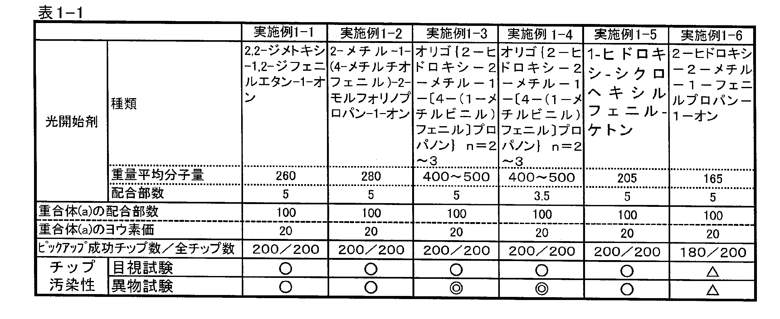

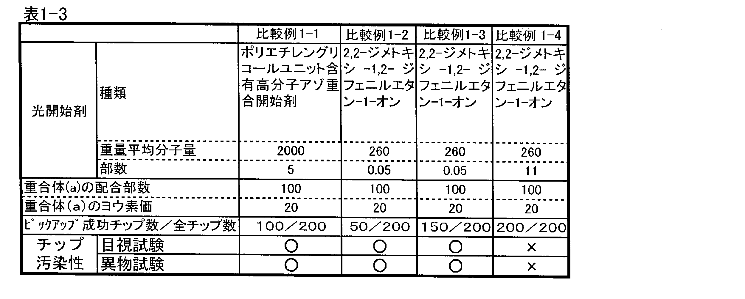
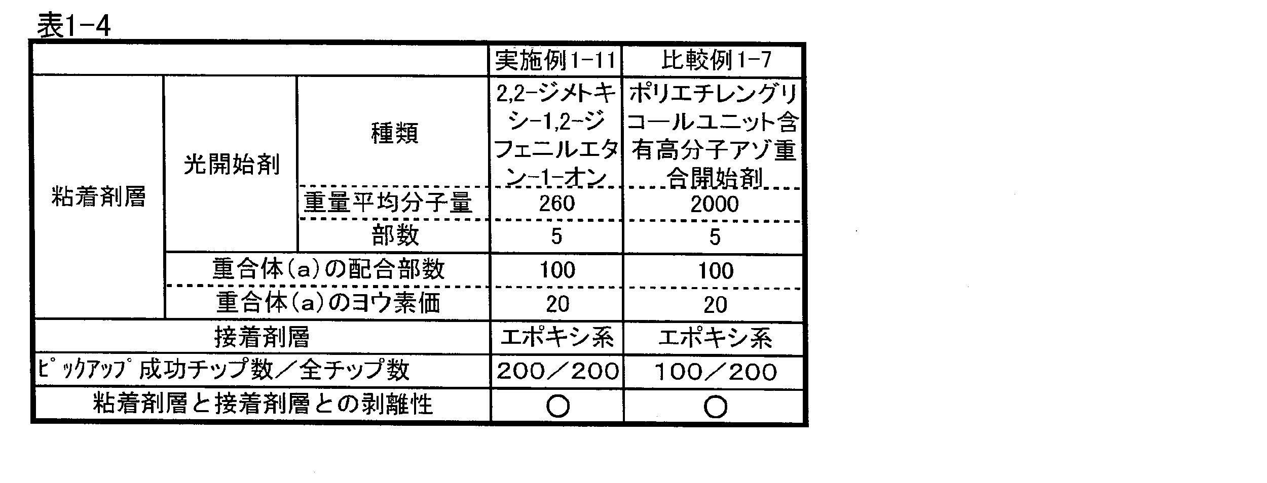
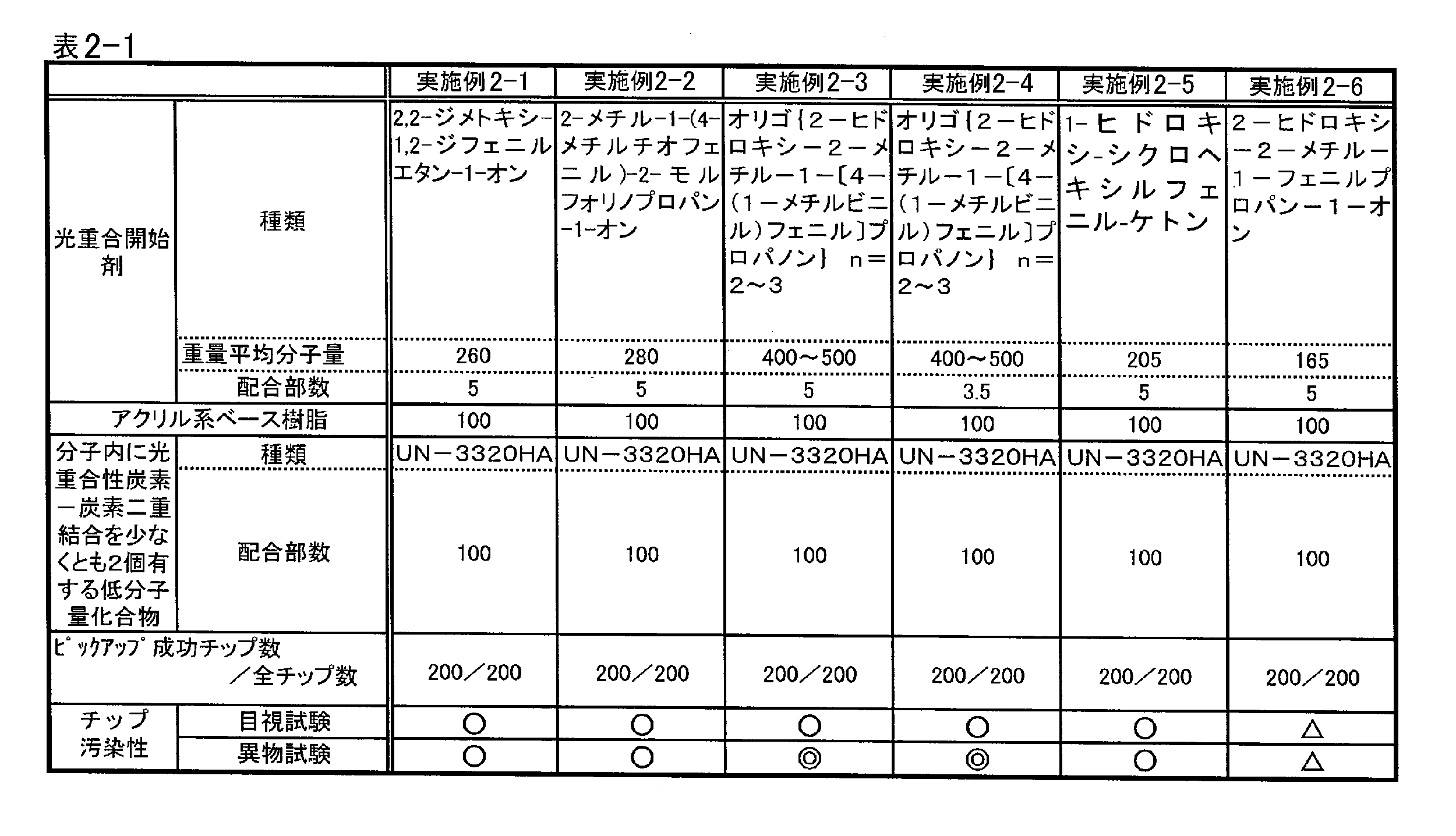
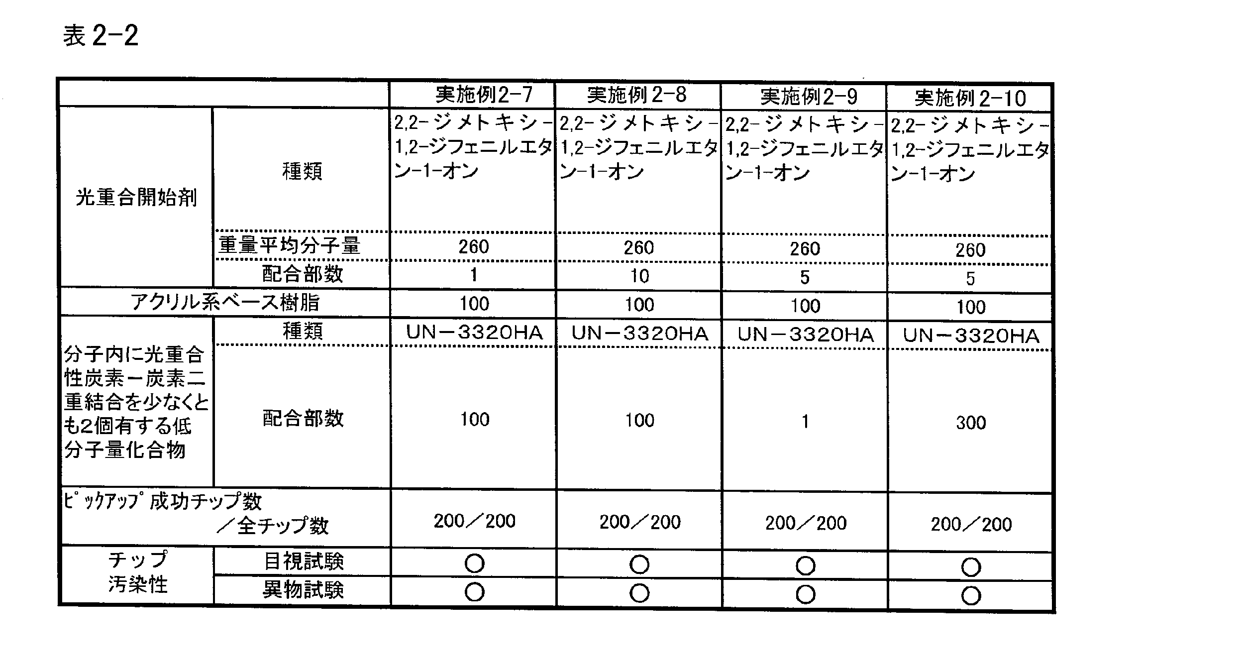
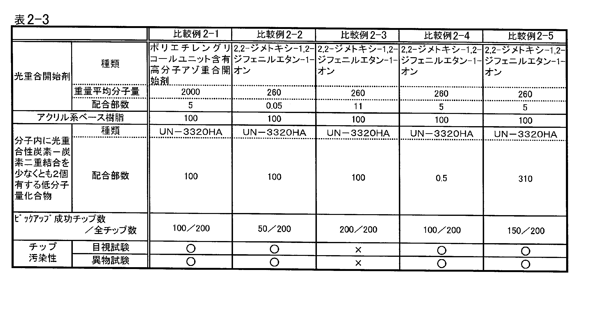
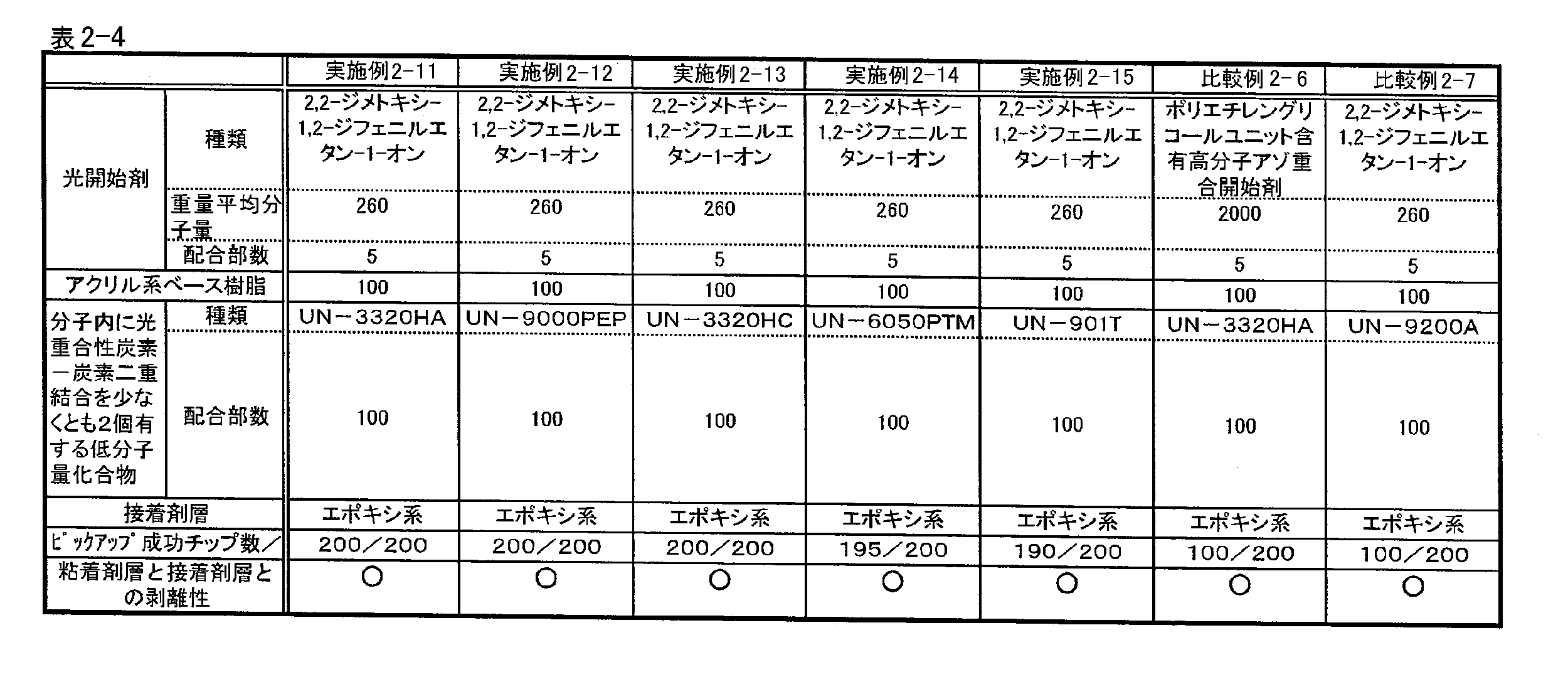
表1-1~1-3からわかるように、図1に示す構成の半導体ウエハ加工用粘着シートについて評価した実施例では、200チップ中、180チップ以上の半導体チップをピックアップでき、チップ汚染や異物残りが少なく、うまくピックアップすることができた。実施例1-6はチップ汚染性や残留異数がややみられたが、実用上問題はないレベルだった。
またベース樹脂としてヨウ素価が0.5の重合体(a)を用いた粘着剤層で構成された半導体ウエハ加工用粘着シートの場合は、200チップ中、180の半導体チップをピックアップでき、合格レベルの特性を示した。
これに対し、光重合開始剤としてポリエチレングリコールユニット含有高分子アゾ重合開始剤を用いたところ(比較例1-1)、光開始剤が十分均一に溶解できず、発生したラジカルの移動が十分円滑に行えない結果、200チップ中半分しかピックアップできなかった。
また、光重合開始剤の量を0.1質量部より少なくした場合(比較例1-2、1-3)、開始剤によるラジカル供給不足により、ピックアップ性に問題が生じ、10質量部より多くした場合(比較例1-4)、未反応物による昇華によりチップ汚染を生じた。
これに対し、比較例1-7では、粘着剤層と接着剤層との間でうまく界面剥離することができず、200チップ中、100の半導体チップしかピックアップすることができなかった。
表2-1~2-3からわかるように、図1に示す構成の半導体ウエハ加工用粘着シートについて評価した実施例では、200チップ中、すべての半導体チップをピックアップでき、チップ汚染や異物残りが少なく、うまくピックアップすることができた。実施例2-6はチップ汚染性や残留異数がややみられたが、実用上問題はないレベルだった。
これに対し、光重合開始剤としてポリエチレングリコールユニット含有高分子アゾ重合開始剤を用いたところ(比較例2-1)、光開始剤が十分均一に溶解できず、発生したラジカルの移動が十分円滑に行えない結果、200チップ中半分しかピックアップできなかった。
また、光重合開始剤の量を0.1質量部より少なくした場合(比較例2-2)、開始剤によるラジカル供給不足により、ピックアップ性に問題が生じ、10質量部より多くした場合(比較例2-3)、未反応物による昇華によりチップ汚染を生じた。
分子内に光重合性炭素-炭素二重結合を少なくとも2個有する化合物の配合部数を1質量部より少なくすると(比較例2-4)、ピックアップ性が低下した。逆に、放射線重合性化合物の配合部数が300質量部より多い場合(比較例2-5)、粘着剤層に硬化収縮が発生し、チップ裏面に粘着剤が密着することにより、ピックアップ性の低下が見られた。
これに対し、重量平均分子量の大きい光重合開始剤を用いた比較例2-6では、粘着剤層と接着剤層との間でうまく界面剥離することができず、200チップ中、100の半導体チップしかピックアップすることができなかった。
また、分子内に光重合性炭素-炭素二重結合を少なくとも2個有する化合物の重量平均分子量が11,500のものを用いた比較例2-7でも、比較例2-6と同様に、200チップ中、100の半導体チップしかピックアップすることができなかった。
2 粘着剤層
3 接着剤層
10、20 半導体ウエハ加工用粘着シート
Claims (6)
- 放射線透過性の基材樹脂フィルムと、該基材樹脂フィルム上に粘着剤層が形成された半導体ウエハ加工用粘着シートであって、該粘着剤層が
(i-1)主鎖の繰り返し単位に対して放射線硬化性炭素-炭素二重結合含有基を有する(メタ)アクリル系単量体部を有する残基を結合したアクリル系重合体(a)を主成分とするベース樹脂100質量部に対し、
(iii)ゲル透過クロマトグラフィ(以下、「GPC」という)法によって、ポリスチレンを標準物質として換算された重量平均分子量が1000未満の光重合開始剤(b)0.1~10質量部
を含有する放射線硬化性樹脂組成物を用いた層で構成されていることを特徴とする半導体ウエハ加工用粘着シート。 - 放射線透過性の基材樹脂フィルムと、該基材樹脂フィルム上に粘着剤層が形成された半導体ウエハ加工用粘着シートであって、該粘着剤層が
(i-2)アクリル系重合体100質量部に対し、
(ii) 分子内に光重合性炭素-炭素二重結合を少なくとも2個有する重量平均分子量が10,000以下の化合物(c)1~300質量部、
(iii)ゲル透過クロマトグラフィ(以下、「GPC」という)法によって、ポリスチレンを標準物質として換算された重量平均分子量が1000未満の光重合開始剤(b)0.1~10質量部
を含有する放射線硬化性樹脂組成物を用いた層で構成されることを特徴とする半導体ウエハ加工用粘着シート。 - 前記光重合開始剤(b)が、1-ヒドロキシ-シクロヘキシルフェニル-ケトン、2,2-ジメトキシ-1,2-ジフェニルエタン-1-オン、2-メチル-1-(4-メチルチオフェニル)-2-モルフォリノプロパン-1-オン、および下記一般式(1)で表されるオリゴマー

(式中、Rはアルキル基を表す。nは整数である。)
からなる群から選ばれる少なくとも1種であることを特徴とする請求項1又は2記載の半導体ウエハ加工用粘着シート。 - 前記一般式(1)で表されるオリゴマーの重合度がn=2~4であることを特徴とする請求項3記載の半導体ウエハ加工用粘着シート。
- 前記主鎖の繰り返し単位に対して放射線重合性炭素-炭素二重結合含有基を有するアクリル系単量体を構成単位として含む重合体(a)のヨウ素価が1~50であることを特徴とする請求項1、3又は4記載の半導体ウエハ加工用粘着シート。
- 請求項1~5のいずれか1項記載の半導体ウエハ加工用粘着シートの粘着剤層上に、さらに接着剤層が設けられたことを特徴とする半導体ウエハ加工用粘着シート。
Priority Applications (3)
| Application Number | Priority Date | Filing Date | Title |
|---|---|---|---|
| SG2012072070A SG184325A1 (en) | 2010-03-31 | 2011-03-29 | Pressure-sensitive adhesive sheet for semiconductor wafer processing |
| KR1020147031373A KR20150001804A (ko) | 2010-03-31 | 2011-03-29 | 다이싱 시트 |
| CN2011800058308A CN102714151A (zh) | 2010-03-31 | 2011-03-29 | 半导体晶片加工用粘合片 |
Applications Claiming Priority (4)
| Application Number | Priority Date | Filing Date | Title |
|---|---|---|---|
| JP2010-084447 | 2010-03-31 | ||
| JP2010084531A JP2011213922A (ja) | 2010-03-31 | 2010-03-31 | 半導体ウエハ加工用粘着シート |
| JP2010-084531 | 2010-03-31 | ||
| JP2010084447A JP2011216734A (ja) | 2010-03-31 | 2010-03-31 | 半導体ウエハ加工用粘着シート |
Publications (1)
| Publication Number | Publication Date |
|---|---|
| WO2011125683A1 true WO2011125683A1 (ja) | 2011-10-13 |
Family
ID=44762628
Family Applications (1)
| Application Number | Title | Priority Date | Filing Date |
|---|---|---|---|
| PCT/JP2011/057912 Ceased WO2011125683A1 (ja) | 2010-03-31 | 2011-03-29 | 半導体ウエハ加工用粘着シート |
Country Status (5)
| Country | Link |
|---|---|
| KR (2) | KR20120092694A (ja) |
| CN (1) | CN102714151A (ja) |
| SG (1) | SG184325A1 (ja) |
| TW (1) | TWI507502B (ja) |
| WO (1) | WO2011125683A1 (ja) |
Cited By (1)
| Publication number | Priority date | Publication date | Assignee | Title |
|---|---|---|---|---|
| CN103525324A (zh) * | 2012-07-06 | 2014-01-22 | 古河电气工业株式会社 | 半导体晶片表面保护用胶带及半导体晶片的制造方法 |
Families Citing this family (6)
| Publication number | Priority date | Publication date | Assignee | Title |
|---|---|---|---|---|
| JP5718515B1 (ja) * | 2014-01-23 | 2015-05-13 | 古河電気工業株式会社 | 半導体ウエハ表面保護用粘着テープおよび半導体ウエハの加工方法 |
| CN107636100B (zh) * | 2015-09-01 | 2019-11-22 | 琳得科株式会社 | 粘合片 |
| WO2018101090A1 (ja) * | 2016-11-29 | 2018-06-07 | リンテック株式会社 | 両面粘着シートおよび半導体装置の製造方法 |
| JP7221479B2 (ja) * | 2018-08-31 | 2023-02-14 | 日化精工株式会社 | ダイシング加工用製剤及び加工処理液 |
| KR102627907B1 (ko) * | 2019-07-30 | 2024-01-19 | 주식회사 엘지화학 | 임시 고정용 점착 시트 및 이를 사용한 반도체 장치의 제조 방법 |
| JP2021095450A (ja) * | 2019-12-13 | 2021-06-24 | 日東電工株式会社 | 半導体加工用粘着シートおよびその利用 |
Citations (7)
| Publication number | Priority date | Publication date | Assignee | Title |
|---|---|---|---|---|
| JPH11293201A (ja) * | 1998-04-10 | 1999-10-26 | Nippon Synthetic Chem Ind Co Ltd:The | 再剥離型粘着剤 |
| JP2003013011A (ja) * | 2001-07-03 | 2003-01-15 | Nitto Denko Corp | 再剥離型粘着剤および再剥離型粘着シート |
| JP2007150206A (ja) * | 2005-11-30 | 2007-06-14 | Furukawa Electric Co Ltd:The | ダイシングテープ |
| JP2007220694A (ja) * | 2005-05-16 | 2007-08-30 | Nitto Denko Corp | ダイシング用粘着シート及びそれを用いた被加工物の加工方法 |
| JP2007220863A (ja) * | 2006-02-16 | 2007-08-30 | Nitto Denko Corp | 活性面貼付ダイシング用粘着テープ又はシートおよび被加工物の切断片のピックアップ方法 |
| JP2009194303A (ja) * | 2008-02-18 | 2009-08-27 | Nitto Denko Corp | ダイシング・ダイボンドフィルム |
| JP2010232629A (ja) * | 2009-03-03 | 2010-10-14 | Hitachi Maxell Ltd | 放射線硬化性粘着剤組成物、それを用いたダイシング用粘着フィルム、及び切断片の製造方法 |
Family Cites Families (3)
| Publication number | Priority date | Publication date | Assignee | Title |
|---|---|---|---|---|
| JP4107417B2 (ja) * | 2002-10-15 | 2008-06-25 | 日東電工株式会社 | チップ状ワークの固定方法 |
| MY138566A (en) * | 2004-03-15 | 2009-06-30 | Hitachi Chemical Co Ltd | Dicing/die bonding sheet |
| ITVA20050049A1 (it) * | 2005-08-05 | 2007-02-06 | Lamberti Spa | Sistemi fotopolimerizzabili contenenti coiniziatori a bassa estraibilita' e volatilita' |
-
2011
- 2011-03-29 WO PCT/JP2011/057912 patent/WO2011125683A1/ja not_active Ceased
- 2011-03-29 KR KR1020127017546A patent/KR20120092694A/ko not_active Ceased
- 2011-03-29 KR KR1020147031373A patent/KR20150001804A/ko not_active Ceased
- 2011-03-29 SG SG2012072070A patent/SG184325A1/en unknown
- 2011-03-29 CN CN2011800058308A patent/CN102714151A/zh active Pending
- 2011-03-30 TW TW100110953A patent/TWI507502B/zh active
Patent Citations (7)
| Publication number | Priority date | Publication date | Assignee | Title |
|---|---|---|---|---|
| JPH11293201A (ja) * | 1998-04-10 | 1999-10-26 | Nippon Synthetic Chem Ind Co Ltd:The | 再剥離型粘着剤 |
| JP2003013011A (ja) * | 2001-07-03 | 2003-01-15 | Nitto Denko Corp | 再剥離型粘着剤および再剥離型粘着シート |
| JP2007220694A (ja) * | 2005-05-16 | 2007-08-30 | Nitto Denko Corp | ダイシング用粘着シート及びそれを用いた被加工物の加工方法 |
| JP2007150206A (ja) * | 2005-11-30 | 2007-06-14 | Furukawa Electric Co Ltd:The | ダイシングテープ |
| JP2007220863A (ja) * | 2006-02-16 | 2007-08-30 | Nitto Denko Corp | 活性面貼付ダイシング用粘着テープ又はシートおよび被加工物の切断片のピックアップ方法 |
| JP2009194303A (ja) * | 2008-02-18 | 2009-08-27 | Nitto Denko Corp | ダイシング・ダイボンドフィルム |
| JP2010232629A (ja) * | 2009-03-03 | 2010-10-14 | Hitachi Maxell Ltd | 放射線硬化性粘着剤組成物、それを用いたダイシング用粘着フィルム、及び切断片の製造方法 |
Cited By (2)
| Publication number | Priority date | Publication date | Assignee | Title |
|---|---|---|---|---|
| CN103525324A (zh) * | 2012-07-06 | 2014-01-22 | 古河电气工业株式会社 | 半导体晶片表面保护用胶带及半导体晶片的制造方法 |
| CN103525324B (zh) * | 2012-07-06 | 2015-04-15 | 古河电气工业株式会社 | 半导体晶片表面保护用胶带及半导体晶片的制造方法 |
Also Published As
| Publication number | Publication date |
|---|---|
| KR20120092694A (ko) | 2012-08-21 |
| KR20150001804A (ko) | 2015-01-06 |
| TW201204800A (en) | 2012-02-01 |
| CN102714151A (zh) | 2012-10-03 |
| TWI507502B (zh) | 2015-11-11 |
| SG184325A1 (en) | 2012-11-29 |
Similar Documents
| Publication | Publication Date | Title |
|---|---|---|
| JP4851613B2 (ja) | 半導体ウエハ表面保護用粘着テープ | |
| KR101840179B1 (ko) | 반도체 웨이퍼 표면 보호용 점착 테이프 및 반도체 웨이퍼의 가공 방법 | |
| CN1163564C (zh) | 压敏粘合剂片及其使用方法 | |
| US20070036930A1 (en) | Pressure-sensitive adhesive sheet, production method thereof and method of processing articles | |
| CN1255522A (zh) | 用于半导体晶片加工的压敏粘合片 | |
| JP7547499B2 (ja) | 粘着テープ及び加工方法 | |
| TWI507502B (zh) | Semiconductor wafer processing adhesive sheet | |
| CN1927978A (zh) | 粘合片和使用该粘合片的制品的加工方法 | |
| CN1927977A (zh) | 粘合片和使用该粘合片的制品的加工方法 | |
| JP5210346B2 (ja) | 粘着シート及び電子部品の製造方法 | |
| WO2016148110A1 (ja) | 半導体ウェハ加工用粘着テープ | |
| WO2016113998A1 (ja) | 樹脂膜形成用シート、樹脂膜形成用複合シート、及びシリコンウエハの再生方法 | |
| TWI891980B (zh) | 作業加工用黏著膠帶 | |
| JP7069116B2 (ja) | バックグラインドテープ用基材 | |
| JP2014209629A (ja) | 半導体ウエハ加工用粘着シート | |
| JP4544658B2 (ja) | 半導体ウエハ保護用粘着シート及び半導体ウエハの研削方法 | |
| JP2005281420A (ja) | 粘着シート | |
| JP2011213922A (ja) | 半導体ウエハ加工用粘着シート | |
| JP7626647B2 (ja) | ワーク加工用粘着テープ | |
| JP5016703B2 (ja) | 粘着シート及び電子部品の製造方法 | |
| CN115141568A (zh) | 支撑片、树脂膜形成用复合片、套件、及带树脂膜的芯片的制造方法 | |
| JP5727811B2 (ja) | 半導体チップのピックアップ方法および半導体装置の製造方法 | |
| JP2011216734A (ja) | 半導体ウエハ加工用粘着シート | |
| JP7766535B2 (ja) | 支持シート、ワーク加工物の製造方法、及びワーク加工物のピックアップ方法 | |
| JP2015008323A (ja) | ダイシングシート |
Legal Events
| Date | Code | Title | Description |
|---|---|---|---|
| WWE | Wipo information: entry into national phase |
Ref document number: 201180005830.8 Country of ref document: CN |
|
| 121 | Ep: the epo has been informed by wipo that ep was designated in this application |
Ref document number: 11765583 Country of ref document: EP Kind code of ref document: A1 |
|
| ENP | Entry into the national phase |
Ref document number: 20127017546 Country of ref document: KR Kind code of ref document: A |
|
| NENP | Non-entry into the national phase |
Ref country code: DE |
|
| 122 | Ep: pct application non-entry in european phase |
Ref document number: 11765583 Country of ref document: EP Kind code of ref document: A1 |