WO2011125641A1 - 薄膜太陽電池およびその製造方法 - Google Patents
薄膜太陽電池およびその製造方法 Download PDFInfo
- Publication number
- WO2011125641A1 WO2011125641A1 PCT/JP2011/057770 JP2011057770W WO2011125641A1 WO 2011125641 A1 WO2011125641 A1 WO 2011125641A1 JP 2011057770 W JP2011057770 W JP 2011057770W WO 2011125641 A1 WO2011125641 A1 WO 2011125641A1
- Authority
- WO
- WIPO (PCT)
- Prior art keywords
- electrode layer
- groove
- solar cell
- film solar
- photoelectric conversion
- Prior art date
- Legal status (The legal status is an assumption and is not a legal conclusion. Google has not performed a legal analysis and makes no representation as to the accuracy of the status listed.)
- Ceased
Links
Images


















Classifications
-
- H—ELECTRICITY
- H10—SEMICONDUCTOR DEVICES; ELECTRIC SOLID-STATE DEVICES NOT OTHERWISE PROVIDED FOR
- H10F—INORGANIC SEMICONDUCTOR DEVICES SENSITIVE TO INFRARED RADIATION, LIGHT, ELECTROMAGNETIC RADIATION OF SHORTER WAVELENGTH OR CORPUSCULAR RADIATION
- H10F77/00—Constructional details of devices covered by this subclass
- H10F77/93—Interconnections
- H10F77/933—Interconnections for devices having potential barriers
- H10F77/935—Interconnections for devices having potential barriers for photovoltaic devices or modules
- H10F77/937—Busbar structures for modules
-
- H—ELECTRICITY
- H10—SEMICONDUCTOR DEVICES; ELECTRIC SOLID-STATE DEVICES NOT OTHERWISE PROVIDED FOR
- H10F—INORGANIC SEMICONDUCTOR DEVICES SENSITIVE TO INFRARED RADIATION, LIGHT, ELECTROMAGNETIC RADIATION OF SHORTER WAVELENGTH OR CORPUSCULAR RADIATION
- H10F19/00—Integrated devices, or assemblies of multiple devices, comprising at least one photovoltaic cell covered by group H10F10/00, e.g. photovoltaic modules
- H10F19/30—Integrated devices, or assemblies of multiple devices, comprising at least one photovoltaic cell covered by group H10F10/00, e.g. photovoltaic modules comprising thin-film photovoltaic cells
- H10F19/31—Integrated devices, or assemblies of multiple devices, comprising at least one photovoltaic cell covered by group H10F10/00, e.g. photovoltaic modules comprising thin-film photovoltaic cells having multiple laterally adjacent thin-film photovoltaic cells deposited on the same substrate
-
- H—ELECTRICITY
- H10—SEMICONDUCTOR DEVICES; ELECTRIC SOLID-STATE DEVICES NOT OTHERWISE PROVIDED FOR
- H10F—INORGANIC SEMICONDUCTOR DEVICES SENSITIVE TO INFRARED RADIATION, LIGHT, ELECTROMAGNETIC RADIATION OF SHORTER WAVELENGTH OR CORPUSCULAR RADIATION
- H10F71/00—Manufacture or treatment of devices covered by this subclass
-
- Y—GENERAL TAGGING OF NEW TECHNOLOGICAL DEVELOPMENTS; GENERAL TAGGING OF CROSS-SECTIONAL TECHNOLOGIES SPANNING OVER SEVERAL SECTIONS OF THE IPC; TECHNICAL SUBJECTS COVERED BY FORMER USPC CROSS-REFERENCE ART COLLECTIONS [XRACs] AND DIGESTS
- Y02—TECHNOLOGIES OR APPLICATIONS FOR MITIGATION OR ADAPTATION AGAINST CLIMATE CHANGE
- Y02E—REDUCTION OF GREENHOUSE GAS [GHG] EMISSIONS, RELATED TO ENERGY GENERATION, TRANSMISSION OR DISTRIBUTION
- Y02E10/00—Energy generation through renewable energy sources
- Y02E10/50—Photovoltaic [PV] energy
Definitions
- the present invention relates to a thin film solar cell and a manufacturing method thereof.
- a transparent conductive film such as SnO 2 , ITO (Indium-Tin Oxide) or ZnO is formed as a first electrode layer on an insulating translucent substrate such as glass.
- a photoelectric conversion layer is formed by stacking a semiconductor p layer, an i layer, and an n layer in this order on the first electrode layer.
- a second electrode layer is formed as a back electrode layer on the photoelectric conversion layer.
- the second electrode layer of the thin-film solar cell is generally a laminated structure in which a transparent electrode layer such as ZnO or ITO is laminated on a layer made of a highly reflective material such as Ag or Al.
- Patent Document 1 Japanese Patent Laid-Open No. 9-83001 (Patent Document 1) is a prior document disclosing an integrated thin film solar cell.
- the non-power generation region that does not contribute to power generation is reduced in order to improve the conversion efficiency of the thin film solar cell.
- a conduction groove is formed using a laser scribing method.
- FIG. 24 is a plan view showing the structure of an integrated thin film solar cell described in Japanese Patent Laid-Open No. 9-83001 (Patent Document 1).
- FIG. 25 is a view as seen from the direction of the arrow XXV-XXV in FIG.
- a transparent conductive film 2 is formed on the glass substrate 1 as a first electrode layer.
- a first separation groove 5 is formed in the first electrode layer 2 using laser irradiation.
- a photoelectric conversion layer 3 is formed on the first electrode layer 2.
- the groove part 6 for contact lines is formed in the photoelectric converting layer 3 using laser irradiation.
- a second electrode layer 4 is formed on the photoelectric conversion layer 3.
- a contact line for connecting the first electrode layer 2 and the second electrode layer 4 is formed in the contact line groove 6.
- a second separation groove 7 is formed in the second electrode layer 4 and the photoelectric conversion layer 3. The power generation region and the output extraction regions P and N are separated by the second separation groove 7.
- a conducting groove 8 is formed in the photoelectric conversion layer 3 and the second electrode layer 4.
- An output extraction electrode 10 is formed by embedding the conductive groove 8 with a conductive material 9.
- An insulating region 30 is provided in order to insulate the periphery of the thin film solar cell.
- the present inventor has found the following problems or sources of problems.
- the intermediate output measurement A larger output may be measured in the final output measurement than the value expected from the result.
- FIG. 26 is a comparative diagram for explaining the problem.
- the point contact terminal is in contact with the second electrode layer at the normal position of the positive electrode side output extraction region P. It is sectional drawing which shows a state. The output of the thin film solar cell is measured by bringing the probe of the measuring instrument into contact with the second electrode layer 4 in each of the positive electrode side output extraction region P and the negative electrode side output extraction region N shown in FIG.
- the positive electrode side and negative electrode side output extraction regions P and N of the thin-film solar cell in which the second separation groove portion 7 and the conduction groove portion 8 are formed are in the range of the width W and in the range of about 1 mm.
- the positive electrode side output extraction region P includes a range of a width W B where the first electrode layer 2 and the second electrode layer 4 are connected, a range of a width W C where four conductive grooves 8 are formed, It is divided into a range of the remaining width W D.
- the width W is the width of a region that does not contribute to the output of the thin film solar cell, it is necessary to reduce the width W in order to improve the output per unit area of the thin film solar cell.
- Width W 8 of the conduction groove 8 formed by the laser irradiation is about 100 [mu] m, distance W A conducting groove 8 adjacent to is about 100 [mu] m. Since the four conducting grooves 8 are formed, the width W C is about 700 ⁇ m. Width W B is approximately 150 [mu] m, is about 150 [mu] m width W D.
- point contact terminal 20A In order to accurately measure the output of the thin-film solar cell by point contact terminal 20A is a probe of the measuring device, it is necessary to contact the point contact terminal 20A and the second electrode layer 4 in the range of the width W B.
- FIG. 27 is a comparative view for explaining the problem, and is a cross-sectional view showing a state in which the point contact terminal is in contact with the thin film solar cell in the power generation region in the intermediate output measurement process in the thin film solar cell.
- the measurement result in the intermediate measurement process is an output excluding one stage of the solar battery cell, and thus may not satisfy the specified value.
- FIG. 28 is a comparative view for explaining the problem, and is a cross-sectional view showing a state in which the point contact terminal is in contact with the second electrode layer in the range of the width W C in the intermediate output measurement step in the thin film solar cell. It is. As shown in FIG. 28, the first electrode layer 2 and the second electrode layer 4 are not connected in the range of the width W C.
- the width is extended through the portion.
- the output of the thin-film solar cell is measured. In this case, since the path for taking out the output of the thin film solar cell becomes longer, the resistance becomes higher, and the measurement result in the intermediate measurement process is lowered.
- the second contact is made with the point contact terminal 20A. Since the electrode layer 4 and the 1st electrode layer 2 are not connected, the output of a thin film solar cell cannot be measured.
- FIG. 29 is a comparative diagram for explaining the problem.
- the surface contact terminal is in contact with the second electrode layer at the normal position of the positive electrode side output extraction region P. It is sectional drawing which shows a state.
- the second electrode 4 faces the contact terminals 22A of the range of the width W B It is necessary to contact at least partly.
- FIG. 30 is a comparative diagram for explaining the problem.
- a part of the surface contact terminal is in contact with the second electrode layer in the power generation region on the positive electrode side output extraction region P side. It is sectional drawing which shows the state which is carrying out.
- the measurement result in the intermediate measurement process is an output excluding one stage of the solar battery cell, and thus may not satisfy the specified value.
- Figure 31 is a comparison diagram for explaining a problem in the intermediate output measuring step in the thin film solar cell, in the scope and width W D of the width W C of the surface contact terminals positive side output extraction region P No. It is sectional drawing which shows the state which is contacting with 2 electrode layers. As shown in FIG. 28, the first electrode layer 2 and the second electrode layer 4 are not connected in the range of the width W C and the range of the width W D.
- the width is extended through the portion.
- the output of the thin-film solar cell is measured. In this case, since the path for taking out the output of the thin film solar cell becomes longer, the resistance becomes higher, and the measurement result in the intermediate measurement process is lowered.
- FIG. 32 is a plan view showing thin-film solar cells separated in a grid pattern.
- 33 is a cross-sectional view of one example viewed from the direction of the arrow XXXIII-XXXIII in FIG. 34 is a cross-sectional view of another example as viewed from the direction of the arrow XXXIV-XXXIV in FIG.
- the second electrode layer 4 and the photoelectric conversion layer 3 are formed in a lattice shape by the second separation groove portion 7 and the groove portion 11 orthogonal to the second separation groove portion 7. Have been separated.
- the thin film solar cell of another example includes the second electrode layer 4, the photoelectric conversion layer 3, and the first electrode by the second separation groove portion 7 and the groove portion 11 orthogonal to the second separation groove portion 7.
- the electrode layer 2 is separated in a grid pattern.
- FIG. 35 is a comparative diagram for explaining the problem.
- the surface contact terminal is in contact with the second electrode layer at the normal position of the negative electrode side output extraction region N. It is sectional drawing which shows a state.
- a range of a width W M where the first electrode layer 2 and the second electrode layer 4 are connected and four conductive grooves 8 are formed. The range is divided into a range of width W N and a range of remaining width W O.
- FIG. 36 is a comparative diagram for explaining the problem.
- a part of the surface contact terminal is in contact with the second electrode layer in the power generation region on the negative electrode side output extraction region N side.
- the output of the thin film solar cell can be measured. it can.
- the surface contact terminals 22B are in contact with each other in the power generation area S, the cell may leak depending on how the surface contact terminals 22B are contacted, thereby reducing the characteristics of the thin-film solar cell. For this reason, it is preferable in terms of production and apparatus configuration that the surface contact terminal 22B is not brought into contact in the power generation area S.
- FIG. 37 is a comparative diagram for explaining the problem.
- the surface contact terminals are the first in the range of the width W N of the negative electrode side output extraction region N and the range of the width W O. It is sectional drawing which shows the state which is contacting with 2 electrode layers. As shown in FIG. 37, the first electrode layer 2 and the second electrode layer 4 are not connected in the range of the width W N and the range of the width W O.
- the present invention has been made in view of the above-described problems.
- An object of the present invention is to provide a thin film solar cell capable of measuring an output and a manufacturing method thereof.
- the manufacturing method of the thin film solar cell based on 1st aspect of this invention forms the photoelectric converting layer on the process of forming a 1st separation groove part in the 1st electrode layer formed on the board
- the method of manufacturing a thin film solar cell includes a step of measuring the output of the power generation region by bringing a measurement terminal into contact with the second electrode layer in the output extraction region separated from the power generation region by the second separation groove;
- the extraction region includes a step of forming a conducting groove in the photoelectric conversion layer and the second electrode layer, and a step of embedding a conductive material in the conducting groove.
- a thin film solar cell according to the first aspect of the present invention is formed on a substrate, a first electrode layer formed on the substrate, a photoelectric conversion layer formed on the first electrode layer, and a photoelectric conversion layer. And a second electrode layer.
- the thin-film solar cell includes a first separation groove that separates the first electrode layer, a contact line that connects the first electrode layer and the second electrode layer, and a second separation groove that separates at least the second electrode layer. It has.
- the thin-film solar cell includes an output extraction region separated from the power generation region by the second separation groove, and a conductive material that penetrates the photoelectric conversion layer and the second electrode layer in the output extraction region and is embedded with a conductive material. And a common groove portion.
- the conducting groove is formed discontinuously at intervals in the length direction of the second separation groove.
- the manufacturing method of the thin film solar cell based on the 2nd aspect of this invention forms the photoelectric converting layer on the process of forming a 1st separation groove part in the 1st electrode layer formed on the board
- the method for manufacturing a thin film solar cell includes a step of forming a second electrode layer on the photoelectric conversion layer and forming a contact line connecting the first electrode layer and the second electrode layer in the contact line groove portion; And a step of forming a second separation groove in at least the second electrode layer.
- the thin-film solar cell manufacturing method includes a conduction groove portion that penetrates the photoelectric conversion layer and the second electrode layer in the output extraction region separated from the power generation region by the second separation groove portion and is embedded with a conductive material. Forming a discontinuity with an interval in the length direction of the second separation groove, a step of measuring the output of the power generation region by bringing a measurement terminal into contact with the second electrode layer in the output extraction region, And embedding a conductive material in the common groove.
- a mask is formed on the second electrode layer in the output extraction region at a predetermined interval, and then the conducting groove is continuously irradiated with a laser.
- the conducting groove in the step of forming the conducting groove, is formed by laser irradiation discontinuously by a laser program.
- the 1st electrode layer connected to the 2nd electrode layer which contacts a measurement terminal in the process of measuring the said output has a 2nd separation groove part in the 2nd electrode layer which contacts a measurement terminal. It is not connected to the second electrode layer opposed to the other.
- the thin film solar cell based on the second aspect of the present invention is formed on a substrate, a first electrode layer formed on the substrate, a photoelectric conversion layer formed on the first electrode layer, and a photoelectric conversion layer. And a second electrode layer.
- the thin-film solar cell also includes a first separation groove that separates the first electrode layer, a contact line groove that connects the first electrode layer and the second electrode layer, and a second separation that separates at least the second electrode layer. And a groove portion.
- the thin-film solar cell includes a conducting groove portion that penetrates the photoelectric conversion layer and the second electrode layer and is embedded with a conductive material in the output extraction region. The conductive groove is formed between adjacent contact line grooves so as to be sandwiched between the contact line grooves when seen in a plan view.
- a thin film solar cell according to the third aspect of the present invention is formed on a substrate, a first electrode layer formed on the substrate, a photoelectric conversion layer formed on the first electrode layer, and a photoelectric conversion layer. And a second electrode layer.
- the thin-film solar cell also includes a first separation groove that separates the first electrode layer, a contact line groove that connects the first electrode layer and the second electrode layer, and a second separation that separates at least the second electrode layer. And a groove portion.
- the thin-film solar cell includes a plurality of conductive grooves that penetrate the photoelectric conversion layer and the second electrode layer and are embedded with a conductive material in the output extraction region.
- the contact line groove portions are formed on both sides of all of the plurality of conduction groove portions so as to sandwich each of the plurality of conduction groove portions in a plan view.
- the present invention it is possible to accurately measure the output of a thin film solar cell during the production of the thin film solar cell in which the area of the output extraction region is reduced to improve the conversion efficiency.
- FIG. 4 is a cross-sectional view showing a state where a surface contact terminal is in contact with a second electrode layer at a normal position in a positive electrode output extraction region P in an intermediate output measurement step in the thin film solar cell of the same embodiment. Section showing a state in which the surface contact terminal is in contact with the second electrode layer in the range of the width W C and the range of the width W D of the positive electrode side output extraction region P in the intermediate output measurement step in the thin film solar cell of the same embodiment.
- FIG. It is sectional drawing which shows the structure of the thin film solar cell which concerns on Embodiment 4 of this invention.
- FIG. 4 is a cross-sectional view showing a state where a surface contact terminal is in contact with a second electrode layer at a normal position in a positive electrode output extraction region P in an intermediate output measurement step in the thin film solar cell of the same embodiment. Section showing a state in which the surface contact terminal is in contact with the second electrode layer in the range of the width W C and the range of the width W D of the positive
- FIG. 4 is a cross-sectional view showing a state in which a point contact terminal is in contact with a second electrode layer at a normal position in a positive electrode output extraction region P in an intermediate output measurement step in the thin film solar cell of the same embodiment.
- a cross-sectional view showing a state in which a point contact terminals in the range of the width W D of the positive electrode side output extraction region P is in contact with the second electrode layer.
- FIG. 4 is a cross-sectional view showing a state in which a point contact terminal is in contact with a second electrode layer in a range of a width W C of a positive electrode output extraction region P in an intermediate output measurement process in the thin film solar cell of the same embodiment.
- FIG. It is a top view which shows the structure of the integrated thin film solar cell described in patent document 1.
- FIG. It is the figure seen from the XXV-XXV line arrow direction of FIG.
- FIG. It is a comparison figure for explaining a subject, and is a sectional view showing the state where a point contact terminal is in contact with a thin film solar cell in a power generation field in an intermediate output measurement process in a thin film solar cell.
- a comparison diagram for explaining a problem in the intermediate output measuring step in the thin film solar cell is a sectional view showing a state in which the point contact terminal is in contact with the second electrode layer in a range of the width W C. It is a comparison figure for explaining a subject, and is a section showing the state where a surface contact terminal is in contact with the 2nd electrode layer in the regular position of positive electrode side output extraction field P in the intermediate output measurement process in a thin film solar cell.
- FIG. It is a comparison figure for explaining a subject, and is the state where a part of surface contact terminal is in contact with the 2nd electrode layer in the electric power generation field on the positive electrode side output extraction field P side in the intermediate output measurement process in a thin film solar cell.
- FIG. 33 is a cross-sectional view of one example viewed from the direction of the arrow of XXXIII-XXXIII in FIG.
- FIG. 33 is a cross-sectional view of another example viewed from the direction of the arrow XXXIV-XXXIV in FIG. 32.
- FIG. 1 It is a comparison figure for explaining a subject, and is a section showing the state where a surface contact terminal is in contact with the 2nd electrode layer in the regular position of negative electrode side output extraction field N in the intermediate output measurement process in a thin film solar cell
- FIG. 1 It is a comparison figure for explaining a subject, and is the state where a part of surface contact terminal is in contact with the 2nd electrode layer in the power generation field at the negative electrode side output extraction field N side in the intermediate output measurement process in a thin film solar cell
- a surface contact terminal is in the range of width W N of negative electrode side output extraction region N, and the range of width W O and the 2nd electrode layer It is sectional drawing which shows the state which is contacting.
- Embodiment 1 the manufacturing method of the thin film solar cell in Embodiment 1 based on this invention is demonstrated with reference to figures.
- the same or corresponding parts in the drawings are denoted by the same reference numerals, and the description thereof will not be repeated.
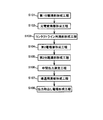
- FIG. 1 is a flowchart showing steps in a method for manufacturing a thin-film solar cell according to Embodiment 1 of the present invention.
- a first separation groove is formed in a first electrode layer formed on a substrate (S101).
- a photoelectric conversion layer is formed on the first electrode layer (S102).
- Contact line grooves are formed in the photoelectric conversion layer (S103).
- a second electrode layer is formed on the photoelectric conversion layer (S104).
- a second separation groove is formed at least in the second electrode layer.
- the output of the power generation region is measured by bringing the measurement terminal into contact with the second electrode layer (S106).
- Conductive grooves are formed in the photoelectric conversion layer and the second electrode layer in the positive electrode side and negative electrode side output extraction regions (S107).
- An output extraction electrode is formed by burying the conductive groove with a conductive material (S108).
- a feature of the method for manufacturing a thin-film solar cell according to the present embodiment is that the step S106 is performed before the step S107. In addition, another process may be performed between each process.
- FIG. 2 is a sectional view showing a state before step S101 in FIG.
- a glass substrate is used as the substrate, but the material of the substrate is not particularly limited as long as it has translucency and insulating properties.
- the material of the first electrode layer 2 is not limited to SnO 2 and may be any material that can be used as a conductive film of a thin film solar cell.
- FIG. 3 is a cross-sectional view showing a state after step S101 in FIG.
- the first electrode layer 2 was patterned using a fundamental wave of a YAG laser.
- the first electrode layer 2 is separated into strips, and the first separation groove 5 is formed in the first electrode layer 2.
- the substrate on which the first separation groove 5 was formed was ultrasonically cleaned with pure water.
- a laser for removing tin oxide (SnO 2 ) a fundamental wave of a fiber laser or YVO 4 laser light may be used.
- FIG. 4 is a cross-sectional view showing a state after step S102 in FIG.
- an amorphous photoelectric conversion layer in which, for example, an a-Si: Hp layer, an a-Si: Hi layer, and an a-Si: Hn layer are sequentially stacked on the first electrode layer 2;
- a photoelectric conversion layer 3 in which a microcrystalline photoelectric conversion layer in which a ⁇ c-Si: Hp layer, a ⁇ c-Si: Hi layer, and a ⁇ c-Si: Hn layer are sequentially stacked is formed.
- a top cell in which a p layer, an i layer, and an n layer made of an amorphous silicon thin film are stacked in this order from the first electrode layer 2 side.
- a middle cell in which a p layer, an i layer and an n layer made of an amorphous silicon thin film are laminated in this order on the top cell, and a p layer, an i layer made of a microcrystalline silicon thin film on the middle cell, and You may use what laminated
- the number of photoelectric conversion layers may be three or more.
- Each of the photoelectric conversion layers may be composed of the same type of silicon-based semiconductor, or may be composed of different types of silicon-based semiconductor.
- Each photoelectric conversion layer from the first photoelectric conversion layer to the third photoelectric conversion layer includes a p-type semiconductor layer, an i-type semiconductor layer, and an n-type semiconductor layer, and each semiconductor layer is formed of a silicon-based semiconductor. It may be.
- Each semiconductor layer included in the photoelectric conversion layer may be composed of the same type of silicon-based semiconductor, or may be composed of different types of silicon-based semiconductor.
- the p-type semiconductor layer and the i-type semiconductor layer may be formed of amorphous silicon, and the n-type semiconductor layer may be formed of microcrystalline silicon.
- the p-type semiconductor layer and the n-type semiconductor layer may be formed of silicon carbide or silicon germanium, and the i-type semiconductor layer may be formed of silicon.
- each of the p-type, i-type and n-type semiconductor layers may have a single layer structure or a multilayer structure. In the case of a multilayer structure, each layer may be composed of different types of silicon-based semiconductors.
- amorphous silicon is a concept including “hydrogenated amorphous silicon”
- microcrystalline silicon is a concept including “hydrogenated microcrystalline silicon”.
- FIG. 5 is a cross-sectional view showing a state after step S103 in FIG.
- the photoelectric conversion layer 3 was patterned using the second harmonic of a YVO 4 laser.
- the contact line groove 6 is formed in the photoelectric conversion layer 3 by making the laser light incident from the glass substrate 1 side.
- the second harmonic of the YVO 4 laser is used.
- patterning may be performed using the second harmonic of the YAG laser.
- FIG. 6 is a cross-sectional view showing the state after step S104 in FIG.
- the second electrode layer 4 made of ZnO / Ag was formed on the photoelectric conversion layer 3 by, for example, magnetron sputtering.
- the second electrode layer 4 was formed with a ZnO film thickness of about 50 nm and an Ag film thickness of about 150 nm.
- a contact line for connecting the first electrode layer 2 and the second electrode layer 4 is formed in the contact line groove 6.
- ZnO / Ag is used as the second electrode layer 4, but a highly light-transmitting film such as ITO (Indium Tin Oxide) or SnO 2 may be used instead of ZnO. Moreover, you may use metals with high reflectance, such as Al, instead of Ag. In the 2nd electrode layer 4, although it is not necessary to provide transparent conductive films, such as ZnO, the conversion efficiency of a thin film solar cell can be improved by providing a transparent conductive film.
- FIG. 7 is a cross-sectional view showing a state after step S105 of FIG.
- the second electrode layer 4 was patterned using the second harmonic of a YVO 4 laser.
- the second separation groove portion 7 is formed in the photoelectric conversion layer 3 and the second electrode layer 4 by making the laser light incident from the glass substrate 1 side.
- the second separation groove portion 7 is also formed in the photoelectric conversion layer 3, but the second separation groove portion 7 may be formed only in the second electrode layer 4.
- FIG. 8 is a cross-sectional view showing a state in which an insulating region is formed around the thin film solar cell.
- the laminate formed on the edge on the glass substrate 1 was removed using the fundamental wave of the YAG laser.
- an insulating region 30 is formed around the thin film solar cell.
- a YAG laser is used, but a mechanical processing method such as blasting may be used.
- FIG. 9 is a cross-sectional view showing a state during step S106 in FIG.
- a thin film solar cell was measured using a solar simulator device as an intermediate measurement.
- the point contact terminal 20A is brought into contact with the second electrode layer 4 in the positive electrode side output extraction region P
- the point contact terminal 20B is brought into contact with the second electrode layer 4 in the negative electrode side output extraction region N to output the power generation region. Measurements were made.
- the first electrode layer 2 connected to the second electrode layer 4 in the positive electrode side output extraction region P through a contact line sandwiches the second separation groove 7 between the second electrode layer 4 in the positive electrode side output extraction region P. It is not connected to the opposing second electrode layer 4.
- the first electrode layer 2 connected to the second electrode layer 4 in the negative electrode side output extraction region N through the contact line has the second separation groove 7 interposed in the second electrode layer 4 in the negative electrode side output extraction region N. It is connected to the second electrode layer 4 facing with the contact line through a contact line.
- the point contact terminal 20A is brought into contact with the second electrode layer 4 in the positive electrode side output extraction region P, and the second electrode layer 4 in the negative electrode side output extraction region N is opposed to the second electrode layer 4 with the second separation groove 7 interposed therebetween. Even when the point contact terminal 20B is brought into contact with the two-electrode layer 4, the output of the power generation region can be measured.
- the second electrode layer 4 in the negative electrode side output extraction region N and the second electrode layer 4 in the negative electrode side output extraction region N are opposed to each other with the second separation groove 7 interposed therebetween. This is because the electrode layer 4 is at the same potential because it is electrically connected.
- the first electrode layer 2 connected to the second electrode layer 4 in the output extraction region through the contact line is connected to the second electrode layer 4 in the output extraction region.
- the output of the power generation region is also obtained when the point contact terminal 20 is brought into contact with the second electrode layer 4 opposed to the separation groove portion 7. Can be measured.
- FIG. 10 is a cross-sectional view showing a state after step S107 in FIG.
- the second electrode layer 4 was patterned in the positive electrode side output extraction region P and the negative electrode side output extraction region N using the second harmonic of the YVO 4 laser.
- Conductive grooves 8 are formed in the photoelectric conversion layer 3 and the second electrode layer 4 by making laser light incident from the glass substrate 1 side.
- the second harmonic of the YVO 4 laser is used.
- patterning may be performed using the second harmonic of the YAG laser.
- FIG. 11 is a cross-sectional view showing a state after step S108 in FIG. As shown in FIG. 11, the conducting groove 8 was embedded with ultrasonic solder. An output extraction electrode was formed by forming a solder-plated copper foil on top of the ultrasonic solder.
- FIG. 12 is a cross-sectional view showing a state where the thin film solar cell is sealed.
- a vacuum laminating apparatus is used in a state where a sealing member 32 is disposed on the back side opposite to the glass substrate 1 with an adhesive member 31 made of transparent ethylene vinyl alcohol as a main raw material.
- the thin film solar cell was sealed.
- As the sealing member 32 a laminated film made of PET (polyethylene terephthalate) / Al / PET was used.
- a terminal box was connected to the thin film solar cell, and the output of the thin film solar cell was measured by a solar simulator device as a final output measurement.
- a solar simulator device As described above, in the manufactured 60000 thin film solar cells, no flaws were observed in the measurement results of the intermediate output measurement and the final output measurement. The reason for this will be described below.
- FIG. 13A is a cross-sectional view showing a state of an intermediate output measurement step of a conventional thin film solar cell.
- FIG. 13B is a cross-sectional view showing a state of the intermediate output measurement step of the thin-film solar cell of the present embodiment.
- the intermediate output measurement is performed after the second separation groove portion 7 and the conduction groove portion 8 are formed. Therefore, in order to make an accurate measurement must be contacted to point contact terminal 20A to the second electrode layer 4 in the region of the width W B.
- the width W B is about 150 [mu] m, it is not easy to contact accurately point contact terminal 20A in this position.
- the intermediate output measurement is performed before the conduction groove 8 is formed. Therefore, in order to perform accurate measurement, the point contact terminal 20A may be brought into contact with the second electrode layer 4 in the region of the width W. As described above, the width W is about 1 mm, and it is not difficult to bring the point contact terminal 20A into contact with this position. Therefore, measurement errors due to variations in contact position between the point contact terminal 20A and the thin film solar cell can be reduced. As a result, accurate measurement can be performed in the intermediate output measurement.
- FIG. 14 is a plan view showing the structure of the thin-film solar cell according to Embodiment 2 of the present invention.
- the output extraction electrode is not shown for simplicity.
- the conducting groove 8 is formed discontinuously at a predetermined interval in the length direction of the second separation groove 7.
- Other configurations are the same as the structure of the thin-film solar cell of Embodiment 1, and thus description thereof will not be repeated.
- the length M of the non-formation region 21 of the conducting groove 8 is preferably larger than the size of the contact portion of the terminal 20 used when the intermediate output measurement is performed with the thin film solar cell. In this way, when the intermediate output measurement is performed, the output of the power generation region can be accurately measured by measuring the terminal 20 in contact with the second electrode layer 4 in the non-formation region 21.
- the thin-film solar cell of this embodiment is separated into strips, but may be separated into a lattice.
- the non-formation region 21 needs to be formed.
- FIG. 15 is a plan view showing a state in which a conduction groove is formed using a mask in the manufacturing process of the thin-film solar cell of the present embodiment.
- the mask 12 is spaced apart on the second electrode layer 4 in the positive electrode side output extraction region P and the negative electrode side output extraction region N.
- the continuous groove 8 is formed by laser irradiation.
- the mask 12 is formed on the second electrode layer 4 in the non-formation region 21.
- the material of the mask 12 is not particularly limited as long as the material does not transmit the laser and is resistant to the laser.
- the formation of the non-forming region 21 may be performed in the process of forming the second separation groove 7 or after the process of forming the second separation groove 7.
- a second harmonic of a YAG laser or a YVO 4 laser can be used.
- the manufacturing method of the thin film solar cell of this embodiment includes the following steps.
- a first separation groove 5 is formed in the first electrode layer 2 formed on the glass substrate 1.
- a photoelectric conversion layer 3 is formed on the first electrode layer 2.
- Contact line grooves 6 are formed in the photoelectric conversion layer 3.
- a second electrode layer 4 is formed on the photoelectric conversion layer 3, and a contact line for connecting the first electrode layer 2 and the second electrode layer 2 is formed in the contact line groove 6.
- the second separation groove 7 is formed at least in the second electrode layer 4. In the positive electrode side and negative electrode side output extraction regions P and N separated from the power generation region by the second separation groove portion 7, the conductive layer 9 penetrates the photoelectric conversion layer 3 and the second electrode layer 4 and is embedded in the conductive material 9.
- the common groove portion 8 is formed discontinuously at intervals in the length direction of the second separation groove portion 7. Separation of the photoelectric conversion layer 3 by the second separation groove 7 enables cells to be connected in series.
- the output of the power generation region is measured by bringing the measurement terminal into contact with the second electrode layer 4 in the positive electrode side and negative electrode side output extraction regions P and N.
- An output extraction electrode 10 is formed by embedding the conducting groove 8 with a conductive material 9. Through this process, a thin film solar cell is completed.
- the conducting groove 8 may be formed by laser irradiation discontinuously by a laser program.
- the Q switch of the laser oscillator so-called electric mask
- the conduction groove 8 and the non-formation region 21 can be formed by discontinuously irradiating the laser.
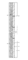
- FIG. 16 is a cross-sectional view seen from the direction of the arrow XVI-XVI in FIG. As shown in FIG. 16, the conducting groove 8 is not formed in the cross section including the non-formation region 21.
- the first electrode layer 2 is formed on the glass substrate 1.
- a photoelectric conversion layer 3 is formed on the first electrode layer 2.
- a second electrode layer 4 is formed on the photoelectric conversion layer 3.
- a first separation groove 5 for separating the first electrode layer 2 is formed.
- a contact line that connects the first electrode layer 2 and the second electrode layer 4 is formed.
- a second separation groove 7 that separates at least the second electrode layer 4 is formed. The power generation region and the positive electrode side and negative electrode side output extraction regions P and N are separated by the second separation groove portion 7.
- a conduction groove portion 8 is formed which penetrates the photoelectric conversion layer 3 and the second electrode layer 4 and is embedded with a conductive material 9 inside.
- the conducting groove portion 8 is formed discontinuously at intervals in the length direction of the second separation groove portion 7.
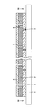
- FIG. 17 is a cross-sectional view showing the structure of a thin-film solar cell according to Embodiment 3 of the present invention.
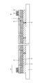
- the conduction groove 8 is formed between the contact line grooves 6 adjacent to each other so as to be sandwiched between the contact line grooves 6 in a plan view. It is formed between.
- the contact line groove 6 is formed on the center side of the thin film solar cell and the contact line groove 13 is formed outside the thin film solar cell so as to sandwich the conduction groove 8 in the positive output extraction region P.
- a contact line groove 6 is formed on the center side of the thin film solar cell, and a contact line groove 14 is formed outside the thin film solar cell so as to sandwich the conduction groove 8 in the negative electrode side output extraction region N.
- the first electrode layer 2 is formed on the glass substrate 1.
- a photoelectric conversion layer 3 is formed on the first electrode layer 2.
- a second electrode layer 4 is formed on the photoelectric conversion layer 3.
- a first separation groove 5 for separating the first electrode layer 2 is formed.
- Contact line grooves 6, 13, 14 for connecting the first electrode layer 2 and the second electrode layer 4 are formed.
- a second separation groove 7 that separates at least the second electrode layer 4 is formed.
- the power generation region and the positive electrode side and negative electrode side output extraction regions P and N are separated by the second separation groove portion 7.
- a conduction groove portion 8 is formed which penetrates the photoelectric conversion layer 3 and the second electrode layer 4 and is embedded with a conductive material 9 inside.
- An output extraction electrode 10 is formed by embedding the conductive groove 8 with a conductive material 9.
- the conductive groove 8 is formed between the contact line groove 6 and the contact line groove 13 or the contact line groove 14 so as to be sandwiched between the contact line grooves 6, 13, 14 in a plan view. Is formed.
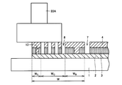
- FIG. 18 is a cross-sectional view showing a state in which the surface contact terminal is in contact with the second electrode layer at a normal position of the positive electrode side output extraction region P in the intermediate output measurement step in the thin film solar cell of the present embodiment.
- the conducting groove 8 is formed before the intermediate output measurement is performed.
- the second electrode layer 4 and the first electrode layer 2 are electrically connected.
- the surface contact terminals 22A in order to measure accurately the intermediate output measurement, it is necessary to contact with the second electrode layer 4 of the scope or width W D of the width W B.
- FIG. 19 shows that the surface contact terminal is in contact with the second electrode layer in the range of the width W C and the width W D of the positive electrode output extraction region P in the intermediate output measurement step in the thin film solar cell of this embodiment. It is sectional drawing which shows a state. As shown in FIG. 19, in the range of the width W D, the first electrode layer 2 and the second electrode layer 4 is connected.
- the surface contact terminals 22A are in the scope and width W D of the width W C of the positive electrode side output extraction region P in contact with the second electrode layer 4 is also possible to accurately measure the output of the power generation region Can do.
- the contact line groove portions 13 and 14 are formed, and the contact line is formed in the contact line groove portions 13 and 14, so that the measurement error due to the variation in the contact position between the terminal 20 and the thin film solar cell. Can be reduced. Since other configurations are the same as those in the first or second embodiment, description thereof will not be repeated.
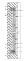
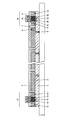
- FIG. 20 is a cross-sectional view showing the structure of a thin-film solar cell according to Embodiment 4 of the present invention.
- the contact line groove portions are formed on both sides of all the plurality of conduction groove portions so as to sandwich each of the plurality of conduction groove portions when viewed in a plan view. Is formed.
- the contact line groove 6 is formed on the center side of the thin film solar cell and the contact line groove 13 is formed outside the thin film solar cell so as to sandwich the conduction groove 8 in the positive output extraction region P.
- a contact line groove 15 is formed between the adjacent conductive grooves 8.
- the contact line groove 15 is preferably formed in the same process as the contact line groove 6 in consideration of productivity.
- the contact line groove 6 is formed on the center side of the thin film solar cell so as to sandwich the conduction groove 8 in the negative electrode side output extraction region N, and the contact line groove 14 is formed outside the thin film solar cell.
- a contact line groove 15 is formed between the adjacent conductive grooves 8 formed. In the present embodiment, since four conductive groove portions 8 in the negative electrode side output extraction region N are formed, three contact line groove portions 15 in the negative electrode side output extraction region N are formed.
- the first electrode layer 2 is formed on the glass substrate 1.
- a first separation groove 5 is formed in the first electrode layer 2.
- a photoelectric conversion layer 3 is formed on the first electrode layer 2.
- a second electrode layer 4 is formed on the photoelectric conversion layer 3.
- a first separation groove 5 for separating the first electrode layer 2 is formed.
- Contact line grooves 6, 13, 14, and 15 connecting the first electrode layer 2 and the second electrode layer 4 are formed.
- a second separation groove 7 that separates at least the second electrode layer 4 is formed. The power generation region and the positive electrode side and negative electrode side output extraction regions P and N are separated by the second separation groove portion 7.
- a plurality of conductive grooves 8 that penetrates the photoelectric conversion layer 3 and the second electrode layer 4 and is embedded in the conductive material 9 are formed.
- An output extraction electrode 10 is formed by embedding a plurality of conductive grooves 8 with a conductive material 9.
- the contact line groove portions 6, 13, 14, and 15 are formed on both sides of all of the plurality of conduction groove portions 8 so as to sandwich each of the plurality of conduction groove portions 8 in plan view.
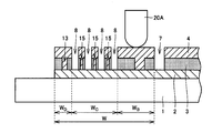
- FIG. 21 is a cross-sectional view showing a state in which the point contact terminal is in contact with the second electrode layer at a normal position of the positive electrode side output extraction region P in the intermediate output measurement step in the thin film solar cell of this embodiment.
- the conducting groove 8 is formed before the intermediate output measurement is performed.
- the range of the width W B, in scope and breadth W D width W C, and the second electrode layer 4 and the first electrode layer 2 are electrically connected.
- the point contact terminal 20A may be brought into contact with the second electrode layer 4 in the range of the width W in order to accurately measure in the intermediate output measurement.
- Figure 22 is the intermediate output measuring step in the thin film solar cell of the present embodiment, a cross sectional view illustrating a state where point contact terminals in the range of the width W D of the positive electrode side output extraction region P is in contact with the second electrode layer is there.
- FIG. 23 is a cross-sectional view showing a state in which the point contact terminal is in contact with the second electrode layer in the range of the width W C of the positive electrode side output extraction region P in the intermediate output measurement step in the thin film solar cell of this embodiment. is there.
- the contact line groove portions 13, 14, 15 are formed, and the contact line is formed in the contact line groove portions 13, 14, 15, so that the contact position between the terminal 20 and the thin-film solar cell is improved. Measurement errors due to variations can be reduced. Since other configurations are similar to those of the first and second embodiments, description thereof will not be repeated.
Landscapes
- Photovoltaic Devices (AREA)
Abstract
基板(1)上に形成された第1電極層(2)に第1分離溝部(5)を形成する工程(S101)と、第1電極層(2)上に光電変換層(3)を形成する工程(S102)と,光電変換層(3)にコンタクトライン用溝部(6)を形成する工程(S103)と、光電変換層(3)上に第2電極層(4)を形成するとともに、コンタクトライン用溝部(6)内に第1電極層(2)と第2電極層(4)とを接続するコンタクトラインを形成する工程(S104)とを備えている。また、少なくとも第2電極層(4)に第2分離溝部(7)を形成する工程(S105)と、第2分離溝部(7)により発電領域と分離された出力取出し領域において、第2電極層(4)に測定端子を接触させることにより、発電領域の出力を測定する工程(S106)とを備えている。さらに、出力取出し領域において、光電変換層(3)および第2電極層(4)に導通用溝部(8)を形成する工程(S107)と、導通用溝部(8)内に導電性材料(9)を埋設する工程(S108)とを備えている。
Description
本発明は、薄膜太陽電池およびその製造方法に関する。
薄膜太陽電池の一般的な構造としては、ガラスなどの絶縁透光性基板上にSnO2、ITO(Indium-Tin Oxide)またはZnOなどの透明導電膜が第1電極層として形成されている。第1電極層上に半導体のp層、i層およびn層がこの順に積層されることにより光電変換層が形成されている。光電変換層上に裏面電極層として第2電極層が形成されている。
薄膜太陽電池の第2電極層としては、AgまたはAlなど反射率の高い材料からなる層の上にZnOまたはITOなどの透明電極層が積層された積層構造とされるのが一般的である。第2電極層を上記の構成にすることにより、太陽電池の変換効率の向上を図っている。
薄膜太陽電池を大面積化するために、レーザ照射を用いて太陽電池の集積化を行ない、個々の太陽電池を直列接続することが一般的になっている。集積化薄膜太陽電池を開示した先行文献として、特開平9-83001号公報(特許文献1)がある。特開平9-83001号公報(特許文献1)に記載された集積化薄膜太陽電池においては、薄膜太陽電池の変換効率を向上させるために、発電に寄与しない非発電領域を削減している。太陽電池の出力取り出し領域の面積を低減するために、レーザスクライブ法を用いて導通溝を形成している。
図24は、特開平9-83001号公報(特許文献1)に記載された集積化薄膜太陽電池の構造を示す平面図である。図25は、図24のXXV-XXV線矢印方向から見た図である。
図24,25に示すように、ガラス基板1上に第1電極層として透明導電膜2が形成されている。レーザ照射を用いて第1電極層2に第1分離溝部5が形成されている。第1電極層2上に光電変換層3が形成されている。
レーザ照射を用いて光電変換層3にコンタクトライン用溝部6が形成されている。光電変換層3上に第2電極層4が形成されている。コンタクトライン用溝部6内に第1電極層2と第2電極層4とを接続するコンタクトラインが形成されている。第2電極層4および光電変換層3に第2分離溝部7が形成されている。第2分離溝7により発電領域と出力取出し領域P,Nとが分離されている。
正極側および負極側出力取出し領域P,Nにおいて、光電変換層3および第2電極層4に導通用溝部8が形成されている。導通用溝部8を導電性材料9で埋設することにより出力取出し電極10が形成されている。なお、薄膜太陽電池の周囲の絶縁を図るために、絶縁領域30が設けられている。
薄膜太陽電池の製造においては、製造途中において上記の発電領域の発電特性の確認が行なわれる。特開平9-83001号公報(特許文献1)に記載された集積化薄膜太陽電池においては、第2分離溝部7と導通用溝部8とを同一の工程において形成した後、出力取出し電極10を形成する前に発電領域の出力を測定している。
本発明者が、上述の技術について検討を行なった結果、以下のような課題または課題の源泉を見出した。上記のように発電領域の出力を測定する中間出力測定工程において測定した結果と、薄膜太陽電池の完成後の最終出力測定工程において測定した結果とに差が出ることがある。具体的には、中間出力測定工程において規定の出力が得られずに不良品と判断された薄膜太陽電池のうち、最終出力測定工程において規定の出力が得られる良品が含まれたり、中間出力測定結果から最終出力を予想した値より最終出力測定にて大きい出力が測定されることがある。
この原因として、薄膜太陽電池の出力を測定する際の測定器のプローブと薄膜太陽電池との接触位置のばらつきによる測定誤差があることが分かった。特に、図24に示す薄膜太陽電池の長さYが大きくなるほど、言い換えると、基板1の大きさが大きくなるほどこの問題が起きやすくなる。
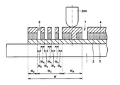
図26は、課題を説明するための比較図であって、薄膜太陽電池における中間出力測定工程において、点接触端子が正極側出力取出し領域Pの正規の位置で第2電極層と接触している状態を示す断面図である。薄膜太陽電池の出力は、図24に示す正極側出力取出し領域Pおよび負極側出力取出し領域Nのそれぞれにおいて、測定器のプローブを第2電極層4に接触させることにより測定する。
図26に示すように、第2分離溝部7と導通用溝部8とを形成した薄膜太陽電池の正極側および負極側出力取出し領域P,Nは、幅Wの範囲となり、約1mmの範囲である。正極側出力取出し領域Pは、第1電極層2と第2電極層4とが接続されている幅WBの範囲と、4つの導通用溝部8が形成されている幅WCの範囲と、残りの幅WDの範囲とに区分けされる。ここで、幅Wは、薄膜太陽電池の出力に寄与しない領域の幅であるため、薄膜太陽電池の単位面積当たりの出力を向上するために幅Wを狭くする必要がある。
レーザ照射で形成した導通用溝部8の幅W8は約100μmであり、隣接する導通用溝部8同士の間隔WAは約100μmである。4つの導通用溝部8が形成されているため、幅WCは約700μmである。幅WBは約150μmであり、幅WDは約150μmである。
測定器のプローブである点接触端子20Aにより薄膜太陽電池の出力を正確に測定するためには、幅WBの範囲において点接触端子20Aと第2電極層4とを接触させる必要がある。
図27は、課題を説明するための比較図であって、薄膜太陽電池における中間出力測定工程において、点接触端子が発電領域で薄膜太陽電池と接触している状態を示す断面図である。図27に示すように、点接触端子20Aが、発電領域において第2電極層4と接触した場合、直列に接続された太陽電池セルの1段分の出力を測定することができなくなる。そのため、中間測定工程における測定結果は、太陽電池セルの1段分を除いた出力となるため規定値を満足しない場合がある。
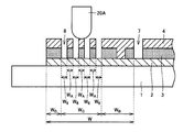
図28は、課題を説明するための比較図であって、薄膜太陽電池における中間出力測定工程において、点接触端子が幅WCの範囲で第2電極層と接触している状態を示す断面図である。図28に示すように、幅WCの範囲においては、第1電極層2と第2電極層4とは接続されていない。
そのため、図24に示すように、正極側出力取出し領域Pの延在方向の端部P1または端部P2に、導通用溝部8が形成されていない部分がある場合は、その部分を通じて幅WCの範囲と幅WBの範囲とが繋がっていることにより、薄膜太陽電池の出力が測定される。この場合は、薄膜太陽電池の出力を取出す経路が長くなるため抵抗が高くなり、中間測定工程における測定結果が低下する。
一方、正極側出力取出し領域Pの延在方向の端部P1または端部P2に、導通用溝部8が形成されていない部分がない場合は、点接触端子20Aと接触している第2電極層4と第1電極層2とが接続されていないため、薄膜太陽電池の出力を測定することができない。
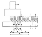
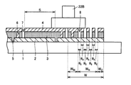
図29は、課題を説明するための比較図であって、薄膜太陽電池における中間出力測定工程において、面接触端子が正極側出力取出し領域Pの正規の位置で第2電極層と接触している状態を示す断面図である。図29に示すように、測定器のプローブである面接触端子22Aを用いて薄膜太陽電池の出力を正確に測定する場合には、面接触端子22Aが幅WBの範囲の第2電極4と少なくとも一部において接触する必要がある。
図30は、課題を説明するための比較図であって、薄膜太陽電池における中間出力測定工程において、面接触端子の一部が正極側出力取出し領域P側の発電領域で第2電極層と接触している状態を示す断面図である。図30に示すように、面接触端子22Aの少なくとも一部が、発電領域において第2電極層4と接触した場合、直列に接続された太陽電池セルの1段分の出力を測定することができなくなる。そのため、中間測定工程における測定結果は、太陽電池セルの1段分を除いた出力となるため規定値を満足しない場合がある。
図31は、課題を説明するための比較図であって、薄膜太陽電池における中間出力測定工程において、面接触端子が正極側出力取出し領域Pの幅WCの範囲および幅WDの範囲で第2電極層と接触している状態を示す断面図である。図28に示すように、幅WCの範囲および幅WDの範囲においては、第1電極層2と第2電極層4とは接続されていない。
そのため、図24に示すように、正極側出力取出し領域Pの延在方向の端部P1または端部P2に、導通用溝部8が形成されていない部分がある場合は、その部分を通じて幅WCの範囲と幅WBの範囲とが繋がっていることにより、薄膜太陽電池の出力が測定される。この場合は、薄膜太陽電池の出力を取出す経路が長くなるため抵抗が高くなり、中間測定工程における測定結果が低下する。
一方、正極側出力取出し領域Pの延在方向の端部P1または端部P2に、導通用溝部8が形成されていない部分がない場合は、面接触端子22Aと接触している第2電極層4と第1電極層2とが接続されていないため、薄膜太陽電池の出力を測定することができない。
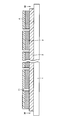
図32は、格子状に分離されている薄膜太陽電池を示す平面図である。図33は、図32のXXXIII-XXXIII線矢印方向から見た一の例の断面図である。図34は、図32のXXXIV-XXXIV線矢印方向から見た他の例の断面図である。
図32,33に示すように、一の例の薄膜太陽電池は、第2分離溝部7と第2分離溝部7に直交する溝部11とにより、第2電極層4および光電変換層3が格子状に分離されている。図32,34に示すように、他の例の薄膜太陽電池は、第2分離溝部7と第2分離溝部7に直交する溝部11とにより、第2電極層4、光電変換層3および第1電極層2が格子状に分離されている。
図31に示すように面接触端子22Aが幅WBの範囲における第2電極層4と接触していない場合、一の例の薄膜太陽電池および他の例の薄膜太陽電池において、正極側出力取出し領域Pの延在方向の両端部以外では、面接触端子22Aと接触している第2電極層4と第1電極層2とが接続されていないため、薄膜太陽電池の出力を測定することができない。
図35は、課題を説明するための比較図であって、薄膜太陽電池における中間出力測定工程において、面接触端子が負極側出力取出し領域Nの正規の位置で第2電極層と接触している状態を示す断面図である。図35に示すように、負極側出力取出し領域Nは、第1電極層2と第2電極層4とが接続されている幅WMの範囲と、4つの導通用溝部8が形成されている幅WNの範囲と、残りの幅WOの範囲とに区分けされる。
薄膜太陽電池の出力を正確に測定する場合には、面接触端子22Bが幅WMの範囲の第2電極4と少なくとも一部に接触する必要がある。
図36は、課題を説明するための比較図であって、薄膜太陽電池における中間出力測定工程において、面接触端子の一部が負極側出力取出し領域N側の発電領域で第2電極層と接触している状態を示す断面図である。図36に示すように、面接触端子22Bが負極側出力取出し領域N側の近傍に位置する発電領域で第2電極層と接触している場合には、薄膜太陽電池の出力を測定することができる。ただし、発電エリアSの範囲において面接触端子22Bが接触している場合には、面接触端子22Bの接触の仕方によって、セルをリークさせて薄膜太陽電池の特性を低下させることがある。そのため、発電エリアSにおいて面接触端子22Bを接触させないことが生産上および装置構成上好ましい。
図37は、課題を説明するための比較図であって、薄膜太陽電池における中間出力測定工程において、面接触端子が負極側出力取出し領域Nの幅WNの範囲および幅WOの範囲で第2電極層と接触している状態を示す断面図である。図37に示すように、幅WNの範囲および幅WOの範囲においては、第1電極層2と第2電極層4とは接続されていない。
そのため、図32に示すように、負極側出力取出し領域Nの延在方向の両端部に、導通用溝部8が形成されていない部分がある場合は、その部分を通じて幅WNの範囲と幅WMの範囲とが繋がっていることにより、薄膜太陽電池の出力が測定される。この場合は、薄膜太陽電池の出力を取出す経路が長くなるため抵抗が高くなり、中間測定工程における測定結果が低下する。
一方、負極側出力取出し領域Nの延在方向の両端部に、導通用溝部8が形成されていない部分がない場合は、面接触端子22Bと接触している第2電極層4と第1電極層2とが接続されていないため、薄膜太陽電池の出力を測定することができない。また、上記の一の例の薄膜太陽電池および他の例の薄膜太陽電池において、負極側出力取出し領域Nの延在方向の両端部以外では、面接触端子22Bと接触している第2電極層4と第1電極層2とが接続されていないため、薄膜太陽電池の出力を測定することができない。
このように、薄膜太陽電池の製造工程の途中において、集積化された大面積の薄膜太陽電池に出力測定用のプローブを精度良く接触させて、正確に発電領域の出力を計測することは容易ではなかった。
本発明は上記の問題点に鑑みてなされたものであって、出力取出し領域の面積を低減して変換効率の向上を図った大面積の薄膜太陽電池の製造途中において、正確に薄膜太陽電池の出力を測定することができる、薄膜太陽電池およびその製造方法を提供することを目的とする。
本発明の第1の局面に基づく薄膜太陽電池の製造方法は、基板上に形成された第1電極層に第1分離溝部を形成する工程と、第1電極層上に光電変換層を形成する工程と、光電変換層にコンタクトライン用溝部を形成する工程とを備えている。また、薄膜太陽電池の製造方法は、光電変換層上に第2電極層を形成するとともに、コンタクトライン用溝部内に第1電極層と第2電極層とを接続するコンタクトラインを形成する工程と、少なくとも第2電極層に第2分離溝部を形成する工程とを備えている。さらに、薄膜太陽電池の製造方法は、第2分離溝により発電領域と分離された出力取出し領域において、第2電極層に測定端子を接触させることにより、発電領域の出力を測定する工程と、出力取出し領域において、光電変換層および第2電極層に導通用溝部を形成する工程と、導通用溝部内に導電性材料を埋設する工程とを備えている。
本発明の第1の局面に基づく薄膜太陽電池は、基板と、基板上に形成された第1電極層と、第1電極層上に形成された光電変換層と、光電変換層上に形成された第2電極層とを備えている。また、薄膜太陽電池は、第1電極層を分離する第1分離溝部と、第1電極層と第2電極層とを接続するコンタクトラインと、少なくとも第2電極層を分離する第2分離溝部とを備えている。さらに、薄膜太陽電池は、第2分離溝部により発電領域と分離された出力取出し領域と、出力取出し領域において、光電変換層および第2電極層を貫通し、内部を導電性材料により埋設された導通用溝部とを備えている。導通用溝部が第2分離溝部の長さ方向に間隔を置いて不連続に形成されている。
本発明の第2の局面に基づく薄膜太陽電池の製造方法は、基板上に形成された第1電極層に第1分離溝部を形成する工程と、第1電極層上に光電変換層を形成する工程と、光電変換層にコンタクトライン用溝部を形成する工程とを備えている。また、薄膜太陽電池の製造方法は、光電変換層上に第2電極層を形成するとともに、コンタクトライン用溝部内に第1電極層と第2電極層とを接続するコンタクトラインを形成する工程と、少なくとも第2電極層に第2分離溝部を形成する工程とを備えている。さらに、薄膜太陽電池の製造方法は、第2分離溝部により発電領域と分離された出力取出し領域において、光電変換層および第2電極層を貫通し、内部を導電性材料により埋設される導通用溝部を第2分離溝部の長さ方向に間隔を置いて不連続に形成する工程と、出力取出し領域における第2電極層に測定端子を接触させることにより、発電領域の出力を測定する工程と、導通用溝部内に導電性材料を埋設する工程とを備える。
本発明の一形態においては、上記導通用溝部を形成する工程において、出力取出し領域における第2電極層上に所定の間隔を置いてマスクを形成した後、連続的にレーザ照射して導通用溝部を形成する。
本発明の一形態においては、上記導通用溝部を形成する工程において、レーザプログラムにより不連続にレーザ照射して導通用溝部を形成する。
本発明の一形態においては、上記出力を測定する工程において測定端子を接触させる第2電極層に接続されている第1電極層は、測定端子を接触させる第2電極層に第2分離溝部を間に挟んで対向する第2電極層に接続されていない。
本発明の第2の局面に基づく薄膜太陽電池は、基板と、基板上に形成された第1電極層と、第1電極層上に形成された光電変換層と、光電変換層上に形成された第2電極層とを備えている。また、薄膜太陽電池は、第1電極層を分離する第1分離溝部と、第1電極層と第2電極層とを接続するコンタクトライン用溝部と、少なくとも第2電極層を分離する第2分離溝部とを備えている。さらに、薄膜太陽電池は、出力取出し領域において、光電変換層および第2電極層を貫通し、内部を導電性材料により埋設された導通用溝部を備えている。導通用溝部は、平面的に見て、コンタクトライン用溝部の間に挟まれるように隣接するコンタクトライン用溝部同士の間に形成されている。
本発明の第3の局面に基づく薄膜太陽電池は、基板と、基板上に形成された第1電極層と、第1電極層上に形成された光電変換層と、光電変換層上に形成された第2電極層とを備えている。また、薄膜太陽電池は、第1電極層を分離する第1分離溝部と、第1電極層と第2電極層とを接続するコンタクトライン用溝部と、少なくとも第2電極層を分離する第2分離溝部とを備えている。さらに、薄膜太陽電池は、出力取出し領域において、光電変換層および第2電極層を貫通し、内部を導電性材料により埋設された複数の導通用溝部を備えている。コンタクトライン用溝部は、平面的に見て、複数の導通用溝部のそれぞれを挟むように全ての複数の導通用溝部の両側に形成されている。
本発明によれば、出力取出し領域の面積を低減して変換効率の向上を図った薄膜太陽電池の製造途中において、正確に薄膜太陽電池の出力を測定することができる。
以下、本発明に基づいた実施形態1における薄膜太陽電池の製造方法について図を参照して説明する。以下の実施形態の説明においては、図中の同一または相当部分には同一符号を付して、その説明は繰返さない。
(実施形態1)
図1は、本発明の実施形態1の薄膜太陽電池の製造方法における工程を示すフロー図である。
図1は、本発明の実施形態1の薄膜太陽電池の製造方法における工程を示すフロー図である。
図1に示すように、本実施形態の薄膜太陽電池の製造方法においては、まず、基板上に形成された第1電極層に第1分離溝部を形成する(S101)。第1電極層上に光電変換層を形成する(S102)。光電変換層にコンタクトライン用溝部を形成する(S103)。光電変換層上に第2電極層を形成する(S104)。少なくとも第2電極層に第2分離溝部を形成する。第2分離溝部により光電変換層を分離することにより、セルを直列接続することが可能になる。また、第2分離溝部により、直列接続されたセルを含む発電領域と正極側および負極側出力取出し領域とが分離される。(S105)。正極側および負極側出力取出し領域において、第2電極層に測定端子を接触させることにより、発電領域の出力を測定する(S106)。正極側および負極側出力取出し領域において、光電変換層および第2電極層に導通用溝部を形成する(S107)。導通用溝部を導電性材料で埋設することにより出力取出し電極を形成する(S108)。
本実施形態の薄膜太陽電池の製造方法の特徴は、上記S106工程をS107工程より先に行なうことである。なお、各工程の間に他の工程が行われてもよい。
図2は、図1のS101工程前の状態を示す断面図である。図2に示すように、基板である、たとえば、厚さ4mm、基板サイズ1000mm×1400mmのガラス基板1上に、熱CVD(Chemical Vapor Deposition)法によりSnO2を主成分とする第1電極層2が形成されている。本実施形態においては、基板としてガラス基板を用いたが、基板の材質は、透光性および絶縁性を有するものであれば特に限られない。また、第1電極層2の材質としては、SnO2に限られず、薄膜太陽電池の導電膜として用いられるものであればよい。
図3は、図1のS101工程後の状態を示す断面図である。図3に示すように、たとえば、YAGレーザの基本波を用いて第1電極層2をパターニングした。レーザ光をガラス基板1側から入射させることにより、第1電極層2は短冊状に分離され、第1電極層2に第1分離溝部5が形成されている。この後、第1分離溝部5が形成された基板を純水で超音波洗浄した。なお、酸化錫(SnO2)を除去するレーザとしては、ファイバーレーザまたはYVO4レーザ光の基本波を用いてもよい。
図4は、図1のS102工程後の状態を示す断面図である。図4に示すように、第1電極層2上に、たとえば、a-Si:Hp層、a-Si:Hi層、a-Si:Hn層が順に積層された非晶質光電変換層と、μc-Si:Hp層、μc-Si:Hi層、μc-Si:Hn層が順に積層された微結晶光電変換層とが積層された光電変換層3が形成されている。
なお、光電変換層3の変形例としては、たとえば、第1電極層2側から、アモルファスシリコン薄膜からなるp層、i層およびn層をこの順に積層したトップセル(第1光電変換層)と、トップセル上に、アモルファスシリコン薄膜からなるp層、i層およびn層をこの順に積層したミドルセル(第2光電変換層)と、ミドルセル上に、微結晶シリコン薄膜からなるp層、i層およびn層をこの順に積層したボトムセル(第3光電変換層)とを、たとえばプラズマCVD法により積層したものを用いてもよい。なお、光電変換層の数を3つ以上とすることもできる。
2つの光電変換層を設けた場合の第1光電変換層から第2光電変換層の各光電変換層、または、3つの光電変換層を設けた場合の第1光電変換層から第3光電変換層の各光電変換層は、全て同種のシリコン系半導体から構成されていてもよく、もしくは、互いに異なる種類のシリコン系半導体から構成されていてもよい。第1光電変換層から第3光電変換層の各光電変換層は、それぞれ、p型半導体層、i型半導体層およびn型半導体層を含んでおり、各半導体層は、シリコン系半導体から構成されていてもよい。光電変換層に含まれる各半導体層は、全て同種のシリコン系半導体から構成されていてもよく、または、互いに異なる種類のシリコン系半導体から構成されていてもよい。
たとえば、p型半導体層とi型半導体層とを非晶質シリコンで形成し、n型半導体層を微結晶シリコンで形成してもよい。また、たとえば、p型半導体層とn型半導体層とをシリコンカーバイドまたはシリコンゲルマニウムで形成し、i型半導体層をシリコンで形成してもよい。さらに、p型、i型およびn型の各半導体層は、単層構造であっても複層構造であってもよい。複層構造である場合、各層は、互いに異なる種類のシリコン系半導体から構成されていてもよい。なお、本明細書において、「非晶質シリコン」は「水素化非晶質シリコン」を含む概念であり、「微結晶シリコン」は「水素化微結晶シリコン」を含む概念である。
図5は、図1のS103工程後の状態を示す断面図である。図5に示すように、YVO4レーザの第2高調波を用いて光電変換層3をパターニングした。レーザ光をガラス基板1側から入射させることにより、光電変換層3にコンタクトライン用溝部6が形成されている。本実施形態においては、YVO4レーザの第2高調波を用いたが、YAGレーザの第2高調波を用いてパターニングを行なってもよい。
図6は、図1のS104工程後の状態を示す断面図である。図6に示すように、光電変換層3上に、たとえば、マグネトロンスパッタ法により、ZnO/Agからなる第2電極層4を形成した。第2電極層4は、ZnOの膜厚を約50nm、Agの膜厚を約150nmとして形成した。このとき、コンタクトライン用溝部6内に第1電極層2と第2電極層4とを接続するコンタクトラインが形成されている。
本実施形態においては、第2電極層4としてZnO/Agを用いたが、ZnOの代わりにITO(Indium Tin Oxide)またはSnO2などの透光性の高い膜を用いていもよい。また、Agの代わりにAlなどの反射率の高い金属を用いてもよい。第2電極層4においては、ZnOなどの透明導電膜を設けなくてもよいが、透明導電膜を設けることにより薄膜太陽電池の変換効率を向上させることができる。
図7は、図1のS105工程後の状態を示す断面図である。図7に示すように、YVO4レーザの第2高調波を用いて第2電極層4をパターニングした。レーザ光をガラス基板1側から入射させることにより、光電変換層3および第2電極層4に第2分離溝部7が形成されている。本実施形態においては、光電変換層3にも第2分離溝部7を形成したが、第2電極層4にのみ第2分離溝部7を形成してもよい。この工程においては、第1電極層2へのダメージを抑えつつ、第2電極層4を構成する銀のバリの発生を抑制する加工条件を選択することが好ましい。
図8は、薄膜太陽電池の周囲に絶縁領域を形成した状態を示す断面図である。図8に示すように、薄膜太陽電池の周囲の絶縁を図るために、YAGレーザの基本波を用いてガラス基板1上の縁に形成されていた積層体を除去した。その結果、薄膜太陽電池の周囲に絶縁領域30が形成されている。本実施形態においては、YAGレーザを用いたが、ブラストなどの機械的処理方法を用いてもよい。
図9は、図1のS106工程中の状態を示す断面図である。図9に示すように、中間測定としてソーラーシミュレータ装置を用いて薄膜太陽電池の測定を行った。このとき、正極側出力取出し領域Pの第2電極層4に点接触端子20Aを接触させ、負極側出力取出し領域Nの第2電極層4に点接触端子20Bを接触させて発電領域の出力の測定を行なった。
正極側出力取出し領域Pの第2電極層4にコンタクトラインを通じて接続されている第1電極層2は、正極側出力取出し領域Pの第2電極層4に第2分離溝部7を間に挟んで対向する第2電極層4に接続されていない。
一方、負極側出力取出し領域Nの第2電極層4にコンタクトラインを通じて接続されている第1電極層2は、負極側出力取出し領域Nの第2電極層4に第2分離溝部7を間に挟んで対向する第2電極層4にコンタクトラインを通じて接続されている。
このため、正極側出力取出し領域Pの第2電極層4に点接触端子20Aを接触させ、負極側出力取出し領域Nの第2電極層4に第2分離溝部7を間に挟んで対向する第2電極層4に点接触端子20Bを接触させた場合においても、発電領域の出力を測定することが可能である。
その理由は、上述したように、負極側出力取出し領域Nの第2電極層4と、負極側出力取出し領域Nの第2電極層4に第2分離溝部7を間に挟んで対向する第2電極層4とは、電気的に接続されているため同電位になっているからである。
上記のように、正極側または負極側にかかわらず、出力取出し領域の第2電極層4にコンタクトラインを通じて接続されている第1電極層2が、出力取出し領域の第2電極層4に第2分離溝部7を間に挟んで対向する第2電極層4にコンタクトラインを通じて接続されている構造においては、この対向する第2電極層4に点接触端子20を接触させた場合も発電領域の出力を測定できる。この場合には、発電領域に含まれるセルがリークしないようにするために、点接触端子20Bと薄膜太陽電池との接触圧力の調整または端子降下速度を低速に制御する必要がある。この接触圧力および端子降下速度の制御は、装置に備えられた全ての端子について適用しなければならないため、出力測定工程のタクト時間が長くなる要因となり、セルに直接端子を接触させることは好ましくはない。
図10は、図1のS107工程後の状態を示す断面図である。図10に示すように、YVO4レーザの第2高調波を用いて、正極側出力取出し領域Pおよび負極側出力取出し領域Nにおいて第2電極層4をパターニングした。レーザ光をガラス基板1側から入射させることにより、光電変換層3および第2電極層4に導通用溝部8が形成されている。本実施形態においては、YVO4レーザの第2高調波を用いたが、YAGレーザの第2高調波を用いてパターニングを行なってもよい。
図11は、図1のS108工程後の状態を示す断面図である。図11に示すように、導通用溝部8を超音波半田によって埋設した。超音波半田の上部に半田めっき銅箔を形成することにより、出力取出し電極を形成した。
図12は、薄膜太陽電池を封止した状態を示す断面図である。図12に示すように、ガラス基板1とは反対側の裏面側に、透明なエチレンビニルアルコールを主原料とする接着部材31を挟んで封止部材32を配置した状態で、真空ラミネート装置を用いて薄膜太陽電池を封止した。封止部材32としては、PET(ポリエチレンテレフタラート)/Al/PETからなる積層フィルムを用いた。
最後に、薄膜太陽電池に端子ボックスを接続し、最終出力測定として薄膜太陽電池の出力をソーラーシミュレータ装置によって測定した。上記のように、製造した薄膜太陽電池セル60000枚において、中間出力測定と最終出力測定との測定結果に齟齬は一枚も認められなかった。この理由を、以下に説明する。
図13Aは、従来の薄膜太陽電池の中間出力測定工程の状態を示す断面図である。図13Bは、本実施形態の薄膜太陽電池の中間出力測定工程の状態を示す断面図である。
図13Aに示すように、従来の薄膜太陽電池の中間出力測定工程においては、第2分離溝部7と導通用溝部8を形成した後に、中間出力測定を行なっている。そのため、正確な測定を行なうためには、点接触端子20Aを幅WBの領域の第2電極層4に接触させなければならない。上述の通り、幅WBは、約150μmであり、この位置に点接触端子20Aを精度良く接触させることは容易ではない。
図13Bに示すように、本実施形態の薄膜太陽電池の中間出力工程においては、導通用溝部8が形成される前に中間出力測定を行なっている。そのため、正確な測定を行なうためには、点接触端子20Aを幅Wの領域の第2電極層4に接触させればよい。上述の通り、幅Wは、約1mmであり、この位置に点接触端子20Aを接触させることは、さほど難しいことではない。よって、点接触端子20Aと薄膜太陽電池との接触位置のばらつきによる測定誤差を低減することができる。その結果、中間出力測定において、正確に測定を行なうことができる。
本実施形態の薄膜太陽電池の製造方法においては、上記のように中間出力測定と最終出力測定との測定結果に差がないため、製造工程のムダを削減して、製造コストの低減を図ることができる。
以下、本発明の実施形態2に係る薄膜太陽電池およびその製造方法について説明する。
(実施形態2)
図14は、本発明の実施形態2に係る薄膜太陽電池の構造を示す平面図である。図14においては、簡単のため、出力取出し電極を図示していない。
(実施形態2)
図14は、本発明の実施形態2に係る薄膜太陽電池の構造を示す平面図である。図14においては、簡単のため、出力取出し電極を図示していない。
図14に示すように、本発明の実施形態2に係る薄膜太陽電池においては、導通用溝部8が第2分離溝部7の長さ方向に所定の間隔を置いて不連続に形成されている。その他の構成については、実施形態1の薄膜太陽電池の構造と同様であるため、説明を繰返さない。
導通用溝部8の非形成領域21の長さMは、中間出力測定を行なう際に用いる端子20の薄膜太陽電池との接触部の大きさより大きいことが好ましい。このようにすることにより、中間出力測定を行なう際に、端子20を非形成領域21の第2電極層4に接触させて測定することにより、発電領域の出力を正確に測定することができる。
本実施形態の薄膜太陽電池は、短冊状に分離されているが、格子状に分離されていてもよい。薄膜太陽電池が格子状に分離されている場合には、導通用溝部8の長さ方向に並ぶ格子状の薄膜太陽電池セルの各列ごとの正極側出力取出し領域Pおよび負極側出力取出し領域Nに、非形成領域21が形成されている必要がある。
図15は、本実施形態の薄膜太陽電池の製造工程において、マスクを用いて導通用溝部を形成する状態を示す平面図である。本実施形態の薄膜太陽電池の製造方法としては、導通用溝部8を形成する工程において、正極側出力取出し領域Pおよび負極側出力取出し領域Nにおける第2電極層4上に間隔を置いてマスク12を形成した後、連続的にレーザ照射して導通用溝部8を形成する。
マスク12は、非形成領域21の第2電極層4上に形成される。マスク12の材料としては、レーザを透過させず、また、レーザに耐性を有する材料であれば特に限定されない。非形成領域21の形成は、第2分離溝部7の形成工程において行なってもよいし、第2分離溝部7の形成工程の後に行なってもよい。レーザとしては、YAGレーザまたはYVO4レーザの第2高調波などが使用できる。
よって、本実施形態の薄膜太陽電池の製造方法は以下の工程を含む。ガラス基板1上に形成された第1電極層2に第1分離溝部5を形成する。第1電極層2上に光電変換層3を形成する。光電変換層3にコンタクトライン用溝部6を形成する。光電変換層3上に第2電極層4を形成するとともに、コンタクトライン用溝部6内に第1電極層2と第2電極層2とを接続するコンタクトラインを形成する。少なくとも第2電極層4に第2分離溝部7を形成する。第2分離溝部7により発電領域と分離された正極側および負極側出力取出し領域P,Nにおいて、光電変換層3および第2電極層4を貫通し、内部を導電性材料9により埋設される導通用溝部8を第2分離溝部7の長さ方向に間隔を置いて不連続に形成する。第2分離溝部7により光電変換層3を分離することにより、セルを直列接続することが可能になる。正極側および負極側出力取出し領域P,Nにおける第2電極層4に測定端子を接触させることにより、発電領域の出力を測定する。導通用溝部8を導電性材料9で埋設することにより出力取出し電極10を形成する。この工程を経て、薄膜太陽電池が完成される。
本実施形態の変形例として、導通用溝部8を形成する工程において、レーザプログラムにより不連続にレーザ照射して導通用溝部8を形成してもよい。レーザ発振器のQスイッチを制御する(いわゆる電気マスク)ことにより、不連続にレーザ照射することにより、導通用溝部8および非形成領域21を形成することができる。
図16は、図14のXVI-XVI線矢印方向から見た断面図である。図16に示すように、非形成領域21を含む断面においては、導通用溝部8が形成されていない。
図14,16に示すように、本実施形態の薄膜太陽電池は、ガラス基板1上に第1電極層2が形成されている。第1電極層2上に光電変換層3が形成されている。光電変換層3上に第2電極層4が形成されている。第1電極層2を分離する第1分離溝部5が形成されている。第1電極層2と第2電極層4とを接続するコンタクトラインが形成されている。少なくとも第2電極層4を分離する第2分離溝部7が形成されている。第2分離溝部7により発電領域と正極側および負極側出力取出し領域P,Nとが分離されている。正極側および負極側出力取出し領域P,Nにおいて、光電変換層3および第2電極層4を貫通し、内部を導電性材料9により埋設された導通用溝部8が形成されている。導通用溝部8が第2分離溝部7の長さ方向に間隔を置いて不連続に形成されている。
本実施形態の構成により、端子20と薄膜太陽電池との接触位置のばらつきによる測定誤差を低減することができる。その結果、中間出力測定において、正確に測定を行なうことができる。
以下、本発明の実施形態3に係る薄膜太陽電池について説明する。
(実施形態3)
図17は、本発明の実施形態3に係る薄膜太陽電池の構造を示す断面図である。図17に示すように、本実施形態の薄膜太陽電池においては、導通用溝部8は、平面的に見て、コンタクトライン用溝部6の間に挟まれるように隣接するコンタクトライン用溝部6同士の間に形成されている。
(実施形態3)
図17は、本発明の実施形態3に係る薄膜太陽電池の構造を示す断面図である。図17に示すように、本実施形態の薄膜太陽電池においては、導通用溝部8は、平面的に見て、コンタクトライン用溝部6の間に挟まれるように隣接するコンタクトライン用溝部6同士の間に形成されている。
具体的には、正極側出力取出し領域Pにおける導通用溝部8を挟むように、薄膜太陽電池の中央側にコンタクトライン用溝部6が形成され、薄膜太陽電池の外側にコンタクトライン用溝部13が形成されている。負極側出力取出し領域Nにおける導通用溝部8を挟むように、薄膜太陽電池の中央側にコンタクトライン用溝部6が形成され、薄膜太陽電池の外側にコンタクトライン用溝部14が形成されている。
よって、本実施形態の薄膜太陽電池は、ガラス基板1上に第1電極層2が形成されている。第1電極層2上に光電変換層3が形成されている。光電変換層3上に第2電極層4が形成されている。第1電極層2を分離する第1分離溝部5が形成されている。第1電極層2と第2電極層4とを接続するコンタクトライン用溝部6,13,14が形成されている。少なくとも第2電極層4を分離する第2分離溝部7が形成されている。第2分離溝部7により発電領域と正極側および負極側出力取出し領域P,Nとが分離されている。正極側および負極側出力取出し領域P,Nにおいて、光電変換層3および第2電極層4を貫通し、内部を導電性材料9により埋設された導通用溝部8が形成されている。導通用溝部8を導電性材料9で埋設することにより出力取出し電極10が形成されている。導通用溝部8は、平面的に見て、コンタクトライン用溝部6,13,14の間に挟まれるように隣接するコンタクトライン用溝部6とコンタクトライン用溝部13またはコンタクトライン用溝部14との間に形成されている。
図18は、本実施形態の薄膜太陽電池における中間出力測定工程において、面接触端子が正極側出力取出し領域Pの正規の位置で第2電極層と接触している状態を示す断面図である。図18に示すように、本実施形態においては、中間出力測定を行なう前に導通用溝部8が形成されている。ただし、幅WBの範囲および幅WDの範囲においては、第2電極層4と第1電極層2とが電気的に接続されている。
そのため、中間出力測定において正確に測定するためには面接触端子22Aを、幅WBの範囲または幅WDの範囲の第2電極層4に接触させる必要がある。
図19は、本実施形態の薄膜太陽電池における中間出力測定工程において、面接触端子が正極側出力取出し領域Pの幅WCの範囲および幅WDの範囲で第2電極層と接触している状態を示す断面図である。図19に示すように、幅WDの範囲においては、第1電極層2と第2電極層4とが接続されている。
そのため、面接触端子22Aが正極側出力取出し領域Pの幅WCの範囲および幅WDの範囲で第2電極層4と接触している場合においても、発電領域の出力を正確に測定することができる。これは、負極側出力取出し領域Nにおいても同様である。このように、コンタクトライン用溝部13,14を形成し、そのコンタクトライン用溝部13,14内にコンタクトラインが形成されていることにより、端子20と薄膜太陽電池との接触位置のばらつきによる測定誤差を低減することができる。他の構成については実施の形態1または2と同様であるため説明を繰返さない。
以下、本発明の実施形態4に係る薄膜太陽電池について説明する。
(実施形態4)
図20は、本発明の実施形態4に係る薄膜太陽電池の構造を示す断面図である。図20に示すように、本実施形態の薄膜太陽電池においては、コンタクトライン用溝部は、平面的に見て、複数の導通用溝部のそれぞれを挟むように全ての複数の導通用溝部の両側に形成されている。
(実施形態4)
図20は、本発明の実施形態4に係る薄膜太陽電池の構造を示す断面図である。図20に示すように、本実施形態の薄膜太陽電池においては、コンタクトライン用溝部は、平面的に見て、複数の導通用溝部のそれぞれを挟むように全ての複数の導通用溝部の両側に形成されている。
具体的には、正極側出力取出し領域Pにおける導通用溝部8を挟むように、薄膜太陽電池の中央側にコンタクトライン用溝部6が形成され、薄膜太陽電池の外側にコンタクトライン用溝部13が形成され、隣接する導通用溝部8同士の間にコンタクトライン用溝部15が形成されている。本実施形態においては、正極側出力取出し領域Pにおける導通用溝部8が4つ形成されているため、正極側出力取出し領域Pにおけるコンタクトライン用溝部15は3つ形成されている。コンタクトライン用溝部15の形成は、コンタクトライン用溝部6の工程と同じ工程で行うことが生産性を考慮すると好ましい。
本実施形態においては、負極側出力取出し領域Nにおける導通用溝部8を挟むように、薄膜太陽電池の中央側にコンタクトライン用溝部6が形成され、薄膜太陽電池の外側にコンタクトライン用溝部14が形成され、隣接する導通用溝部8同士の間にコンタクトライン用溝部15が形成されている。本実施形態においては、負極側出力取出し領域Nにおける導通用溝部8が4つ形成されているため、負極側出力取出し領域Nにおけるコンタクトライン用溝部15は3つ形成されている。
よって、本実施形態の薄膜太陽電池は、ガラス基板1上に第1電極層2が形成されている。第1電極層2に第1分離溝部5が形成されている。第1電極層2上に光電変換層3が形成されている。光電変換層3上に第2電極層4が形成されている。第1電極層2を分離する第1分離溝部5が形成されている。第1電極層2と第2電極層4とを接続するコンタクトライン用溝部6,13,14,15が形成されている。少なくとも第2電極層4を分離する第2分離溝部7が形成されている。第2分離溝部7により発電領域と正極側および負極側出力取出し領域P,Nとが分離されている。正極側および負極側出力取出し領域P,Nにおいて、光電変換層3および第2電極層4を貫通し、内部を導電性材料9により埋設された複数の導通用溝部8が形成されている。複数の導通用溝部8を導電性材料9で埋設することにより出力取出し電極10が形成されている。コンタクトライン用溝部6,13,14,15は、平面的に見て、複数の導通用溝部8のそれぞれを挟むように全ての複数の導通用溝部8の両側に形成されている。
図21は、本実施形態の薄膜太陽電池における中間出力測定工程において、点接触端子が正極側出力取出し領域Pの正規の位置で第2電極層と接触している状態を示す断面図である。図21に示すように、本実施形態においては、中間出力測定を行なう前に導通用溝部8が形成されている。ただし、幅WBの範囲、幅WCの範囲および幅WDの範囲においては、第2電極層4と第1電極層2とが電気的に接続されている。
そのため、中間出力測定において正確に測定するためには点接触端子20Aを、幅Wの範囲の第2電極層4に接触させればよい。
図22は、本実施形態の薄膜太陽電池における中間出力測定工程において、点接触端子が正極側出力取出し領域Pの幅WDの範囲で第2電極層と接触している状態を示す断面図である。図23は、本実施形態の薄膜太陽電池における中間出力測定工程において、点接触端子が正極側出力取出し領域Pの幅WCの範囲で第2電極層と接触している状態を示す断面図である。
図21に示すように点接触端子20Aが幅WBの範囲の第2電極層4に接触している場合、図22に示すように点接触端子20Aが幅WDの範囲の第2電極層4に接触している場合、図23に示すように点接触端子20Aが幅WCの範囲の第2電極層4に接触している場合の、いずれの場合にも発電領域の出力を正確に測定することができる。
このように、コンタクトライン用溝部13,14,15を形成し、そのコンタクトライン用溝部13,14,15内にコンタクトラインが形成されていることにより、端子20と薄膜太陽電池との接触位置のばらつきによる測定誤差を低減することができる。他の構成については実施の形態1および2と同様であるため説明を繰返さない。
なお、今回開示した上記実施形態はすべての点で例示であって、限定的な解釈の根拠となるものではない。したがって、本発明の技術的範囲は、上記した実施形態のみによって解釈されるものではなく、請求の範囲の記載に基づいて画定される。また、請求の範囲と均等の意味および範囲内でのすべての変更が含まれる。
1 ガラス基板、2 第1電極層、3 光電変換層、4 第2電極層、5 第1分離溝部、6,13,14,15 コンタクトライン用溝部、7 第2分離溝部、8 導通用溝部、9 導電性材料、10 出力取出し電極、12 マスク、20 端子、20A,20B 点接触端子、21 非形成領域、22A 面接触端子、30 絶縁領域、31 接着部材、32 封止部材。
Claims (8)
- 基板(1)上に形成された第1電極層(2)に第1分離溝部(5)を形成する工程と、
前記第1電極層(2)上に光電変換層(3)を形成する工程と、
前記光電変換層(3)にコンタクトライン用溝部(6)を形成する工程と、
前記光電変換層(3)上に第2電極層(4)を形成するとともに、前記コンタクトライン用溝部(6)内に前記第1電極層(2)と前記第2電極層(4)とを接続するコンタクトラインを形成する工程と、
少なくとも前記第2電極層(4)に第2分離溝部(7)を形成する工程と、
前記第2分離溝部(7)により発電領域と分離された出力取出し領域において、前記第2電極層(4)に測定端子を接触させることにより、前記発電領域の出力を測定する工程と、
前記出力取出し領域において、前記光電変換層(3)および前記第2電極層(4)に導通用溝部(8)を形成する工程と、
前記導通用溝部(8)内に導電性材料(9)を埋設する工程と
を備える、薄膜太陽電池の製造方法。 - 基板(1)と、
前記基板(1)上に形成された第1電極層(2)と、
前記第1電極層(2)上に形成された光電変換層(3)と、
前記光電変換層(3)上に形成された第2電極層(4)と、
前記第1電極層(2)を分離する第1分離溝部(5)と、
前記第1電極層(2)と前記第2電極層(4)とを接続するコンタクトラインと、
少なくとも前記第2電極層(4)を分離する第2分離溝部(7)と、
前記第2分離溝部(7)により発電領域と分離された出力取出し領域と、
前記出力取出し領域において、前記光電変換層(3)および前記第2電極層(4)を貫通し、内部を導電性材料(9)により埋設された導通用溝部(8)と
を備え、
前記導通用溝部(8)が前記第2分離溝部(7)の長さ方向に間隔を置いて不連続に形成されている、薄膜太陽電池。 - 基板(1)上に形成された前記第1電極層(2)に第1分離溝部(5)を形成する工程と、
前記第1電極層(2)上に光電変換層(3)を形成する工程と、
前記光電変換層(3)にコンタクトライン用溝部(6)を形成する工程と、
前記光電変換層(3)上に第2電極層(4)を形成するとともに、前記コンタクトライン用溝部(6,13,14)内に前記第1電極層(2)と前記第2電極層(4)とを接続するコンタクトラインを形成する工程と、
少なくとも前記第2電極層(4)に第2分離溝部(7)を形成する工程と、
前記第2分離溝部(7)により発電領域と分離された出力取出し領域において、前記光電変換層(3)および前記第2電極層(4)を貫通し、内部を導電性材料(9)により埋設される導通用溝部(8)を前記第2分離溝部(7)の長さ方向に間隔を置いて不連続に形成する工程と、
前記出力取出し領域における前記第2電極層(4)に測定端子を接触させることにより、前記発電領域の出力を測定する工程と
前記導通用溝部(8)内に導電性材料(9)を埋設する工程と
を備える、薄膜太陽電池の製造方法。 - 前記導通用溝部(8)を形成する工程において、前記出力取出し領域における前記第2電極層(4)上に所定の間隔を置いてマスク(12)を形成した後、連続的にレーザ照射して前記導通用溝部(8)を形成する、請求項3に記載の薄膜太陽電池の製造方法。
- 前記導通用溝部(8)を形成する工程において、レーザプログラムにより不連続にレーザ照射して前記導通用溝部(8)を形成する、請求項3に記載の薄膜太陽電池の製造方法。
- 前記出力を測定する工程において前記測定端子を接触させる前記第2電極層(4)に接続されている前記第1電極層(2)は、前記測定端子を接触させる前記第2電極層(4)に前記第2分離溝部(7)を間に挟んで対向する前記第2電極層(4)に接続されていない、請求項1,3,4および5のいずれかに記載の薄膜太陽電池の製造方法。
- 基板(1)と、
前記基板(1)上に形成された第1電極層(2)と、
前記第1電極層(2)上に形成された光電変換層(3)と、
前記光電変換層(3)上に形成された第2電極層(4)と、
前記第1電極層(2)を分離する第1分離溝部(5)と、
前記第1電極層(2)と前記第2電極層(4)とを接続するコンタクトライン用溝部(6,13,14)と、
少なくとも前記第2電極層(4)を分離する第2分離溝部(7)と、
前記出力取出し領域において、前記光電変換層(3)および前記第2電極層(4)を貫通し、内部を導電性材料(9)により埋設された導通用溝部(8)と
を備え、
前記導通用溝部(8)は、平面的に見て、前記コンタクトライン用溝部(6,13,14)の間に挟まれるように隣接する前記コンタクトライン用溝部同士の間に形成されている、薄膜太陽電池。 - 基板(1)と、
前記基板(1)上に形成された第1電極層(2)と、
前記第1電極層(2)上に形成された光電変換層(3)と、
前記光電変換層(3)上に形成された第2電極層(4)と、
前記第1電極層(2)を分離する第1分離溝部(5)と、
前記第1電極層(2)と前記第2電極層(4)とを接続するコンタクトライン用溝部(6,13,14,15)と、
少なくとも前記第2電極層(4)を分離する第2分離溝部(7)と、
前記出力取出し領域において、前記光電変換層(3)および前記第2電極層(4)を貫通し、内部を導電性材料(9)により埋設された複数の導通用溝部(8)と
を備え、
前記コンタクトライン用溝部(6,13,14,15)は、平面的に見て、前記複数の導通用溝部(8)のそれぞれを挟むように全ての前記複数の導通用溝部(8)の両側に形成されている、薄膜太陽電池。
Applications Claiming Priority (2)
| Application Number | Priority Date | Filing Date | Title |
|---|---|---|---|
| JP2010089462A JP4986087B2 (ja) | 2010-04-08 | 2010-04-08 | 薄膜太陽電池およびその製造方法 |
| JP2010-089462 | 2010-04-08 |
Publications (1)
| Publication Number | Publication Date |
|---|---|
| WO2011125641A1 true WO2011125641A1 (ja) | 2011-10-13 |
Family
ID=44762588
Family Applications (1)
| Application Number | Title | Priority Date | Filing Date |
|---|---|---|---|
| PCT/JP2011/057770 Ceased WO2011125641A1 (ja) | 2010-04-08 | 2011-03-29 | 薄膜太陽電池およびその製造方法 |
Country Status (2)
| Country | Link |
|---|---|
| JP (1) | JP4986087B2 (ja) |
| WO (1) | WO2011125641A1 (ja) |
Cited By (1)
| Publication number | Priority date | Publication date | Assignee | Title |
|---|---|---|---|---|
| JP2014222775A (ja) * | 2011-10-13 | 2014-11-27 | エルジー エレクトロニクス インコーポレイティド | 薄膜太陽電池モジュール及び製造方法 |
Citations (2)
| Publication number | Priority date | Publication date | Assignee | Title |
|---|---|---|---|---|
| JP3613851B2 (ja) * | 1995-09-14 | 2005-01-26 | 株式会社カネカ | 集積化薄膜太陽電池 |
| JP2008140885A (ja) * | 2006-11-30 | 2008-06-19 | Mitsubishi Heavy Ind Ltd | 太陽電池パネル製造システム及び太陽電池パネル製造方法 |
-
2010
- 2010-04-08 JP JP2010089462A patent/JP4986087B2/ja not_active Expired - Fee Related
-
2011
- 2011-03-29 WO PCT/JP2011/057770 patent/WO2011125641A1/ja not_active Ceased
Patent Citations (2)
| Publication number | Priority date | Publication date | Assignee | Title |
|---|---|---|---|---|
| JP3613851B2 (ja) * | 1995-09-14 | 2005-01-26 | 株式会社カネカ | 集積化薄膜太陽電池 |
| JP2008140885A (ja) * | 2006-11-30 | 2008-06-19 | Mitsubishi Heavy Ind Ltd | 太陽電池パネル製造システム及び太陽電池パネル製造方法 |
Cited By (2)
| Publication number | Priority date | Publication date | Assignee | Title |
|---|---|---|---|---|
| JP2014222775A (ja) * | 2011-10-13 | 2014-11-27 | エルジー エレクトロニクス インコーポレイティド | 薄膜太陽電池モジュール及び製造方法 |
| US9246040B2 (en) | 2011-10-13 | 2016-01-26 | Lg Electronics Inc. | Thin film solar cell module and method for manufacturing the same |
Also Published As
| Publication number | Publication date |
|---|---|
| JP2011222695A (ja) | 2011-11-04 |
| JP4986087B2 (ja) | 2012-07-25 |
Similar Documents
| Publication | Publication Date | Title |
|---|---|---|
| WO2004064167A1 (ja) | 透光性薄膜太陽電池モジュールおよびその製造方法 | |
| JP2014017447A (ja) | 集積型薄膜太陽電池およびその製造方法 | |
| KR20100088182A (ko) | 태양전지 모듈 및 이의 제조 방법 | |
| JP4762100B2 (ja) | 太陽電池モジュール | |
| JP5702472B2 (ja) | 合わせガラス構造太陽電池モジュール | |
| JP2005277113A (ja) | 積層型太陽電池モジュール | |
| JP3815875B2 (ja) | 集積型薄膜光電変換装置の製造方法 | |
| WO2008026581A1 (fr) | Module de pile solaire | |
| JP2010062186A (ja) | 光電変換装置およびその製造方法 | |
| US8962983B2 (en) | Laminated body having semiconductor layer and layer thickness measurement portion, and thin-film photoelectric conversion device and integrated thin-film solar cell having the same | |
| JPH1079522A (ja) | 薄膜光電変換装置およびその製造方法 | |
| JP5209017B2 (ja) | 薄膜太陽電池および薄膜太陽電池の製造方法 | |
| US20120040488A1 (en) | Method of forming photovoltaic modules | |
| JP4986087B2 (ja) | 薄膜太陽電池およびその製造方法 | |
| JP5134075B2 (ja) | 薄膜太陽電池の製造方法 | |
| JP4261169B2 (ja) | 透光性薄膜太陽電池及び透光性薄膜太陽電池モジュールの製造方法 | |
| JP4112202B2 (ja) | 薄膜太陽電池の製造方法 | |
| JPH0883919A (ja) | 太陽電池モジュール及びその製造方法 | |
| JP2013058702A (ja) | 太陽電池セルおよびその製造方法、太陽電池モジュールおよびその製造方法 | |
| WO2014103513A1 (ja) | 太陽電池モジュールおよび太陽電池モジュールの製造方法 | |
| JP2001127319A (ja) | 太陽電池モジュール及びその製造方法 | |
| JP5539081B2 (ja) | 集積型薄膜光電変換装置の製造方法 | |
| JPH0779004A (ja) | 薄膜太陽電池 | |
| JP5084868B2 (ja) | 薄膜太陽電池の製造方法 | |
| JP4077456B2 (ja) | 集積化薄膜太陽電池 |
Legal Events
| Date | Code | Title | Description |
|---|---|---|---|
| 121 | Ep: the epo has been informed by wipo that ep was designated in this application |
Ref document number: 11765541 Country of ref document: EP Kind code of ref document: A1 |
|
| NENP | Non-entry into the national phase |
Ref country code: DE |
|
| 122 | Ep: pct application non-entry in european phase |
Ref document number: 11765541 Country of ref document: EP Kind code of ref document: A1 |