WO2011125444A1 - 液晶表示装置 - Google Patents
液晶表示装置 Download PDFInfo
- Publication number
- WO2011125444A1 WO2011125444A1 PCT/JP2011/056303 JP2011056303W WO2011125444A1 WO 2011125444 A1 WO2011125444 A1 WO 2011125444A1 JP 2011056303 W JP2011056303 W JP 2011056303W WO 2011125444 A1 WO2011125444 A1 WO 2011125444A1
- Authority
- WO
- WIPO (PCT)
- Prior art keywords
- electrode
- liquid crystal
- pixel
- display
- transmissive
- Prior art date
- Legal status (The legal status is an assumption and is not a legal conclusion. Google has not performed a legal analysis and makes no representation as to the accuracy of the status listed.)
- Ceased
Links
Images





Classifications
-
- G—PHYSICS
- G02—OPTICS
- G02F—OPTICAL DEVICES OR ARRANGEMENTS FOR THE CONTROL OF LIGHT BY MODIFICATION OF THE OPTICAL PROPERTIES OF THE MEDIA OF THE ELEMENTS INVOLVED THEREIN; NON-LINEAR OPTICS; FREQUENCY-CHANGING OF LIGHT; OPTICAL LOGIC ELEMENTS; OPTICAL ANALOGUE/DIGITAL CONVERTERS
- G02F1/00—Devices or arrangements for the control of the intensity, colour, phase, polarisation or direction of light arriving from an independent light source, e.g. switching, gating or modulating; Non-linear optics
- G02F1/01—Devices or arrangements for the control of the intensity, colour, phase, polarisation or direction of light arriving from an independent light source, e.g. switching, gating or modulating; Non-linear optics for the control of the intensity, phase, polarisation or colour
- G02F1/13—Devices or arrangements for the control of the intensity, colour, phase, polarisation or direction of light arriving from an independent light source, e.g. switching, gating or modulating; Non-linear optics for the control of the intensity, phase, polarisation or colour based on liquid crystals, e.g. single liquid crystal display cells
- G02F1/133—Constructional arrangements; Operation of liquid crystal cells; Circuit arrangements
- G02F1/1333—Constructional arrangements; Manufacturing methods
- G02F1/1335—Structural association of cells with optical devices, e.g. polarisers or reflectors
- G02F1/133553—Reflecting elements
- G02F1/133555—Transflectors
-
- G—PHYSICS
- G02—OPTICS
- G02F—OPTICAL DEVICES OR ARRANGEMENTS FOR THE CONTROL OF LIGHT BY MODIFICATION OF THE OPTICAL PROPERTIES OF THE MEDIA OF THE ELEMENTS INVOLVED THEREIN; NON-LINEAR OPTICS; FREQUENCY-CHANGING OF LIGHT; OPTICAL LOGIC ELEMENTS; OPTICAL ANALOGUE/DIGITAL CONVERTERS
- G02F1/00—Devices or arrangements for the control of the intensity, colour, phase, polarisation or direction of light arriving from an independent light source, e.g. switching, gating or modulating; Non-linear optics
- G02F1/01—Devices or arrangements for the control of the intensity, colour, phase, polarisation or direction of light arriving from an independent light source, e.g. switching, gating or modulating; Non-linear optics for the control of the intensity, phase, polarisation or colour
- G02F1/13—Devices or arrangements for the control of the intensity, colour, phase, polarisation or direction of light arriving from an independent light source, e.g. switching, gating or modulating; Non-linear optics for the control of the intensity, phase, polarisation or colour based on liquid crystals, e.g. single liquid crystal display cells
- G02F1/133—Constructional arrangements; Operation of liquid crystal cells; Circuit arrangements
- G02F1/1333—Constructional arrangements; Manufacturing methods
- G02F1/1343—Electrodes
- G02F1/134309—Electrodes characterised by their geometrical arrangement
-
- G—PHYSICS
- G02—OPTICS
- G02F—OPTICAL DEVICES OR ARRANGEMENTS FOR THE CONTROL OF LIGHT BY MODIFICATION OF THE OPTICAL PROPERTIES OF THE MEDIA OF THE ELEMENTS INVOLVED THEREIN; NON-LINEAR OPTICS; FREQUENCY-CHANGING OF LIGHT; OPTICAL LOGIC ELEMENTS; OPTICAL ANALOGUE/DIGITAL CONVERTERS
- G02F1/00—Devices or arrangements for the control of the intensity, colour, phase, polarisation or direction of light arriving from an independent light source, e.g. switching, gating or modulating; Non-linear optics
- G02F1/01—Devices or arrangements for the control of the intensity, colour, phase, polarisation or direction of light arriving from an independent light source, e.g. switching, gating or modulating; Non-linear optics for the control of the intensity, phase, polarisation or colour
- G02F1/13—Devices or arrangements for the control of the intensity, colour, phase, polarisation or direction of light arriving from an independent light source, e.g. switching, gating or modulating; Non-linear optics for the control of the intensity, phase, polarisation or colour based on liquid crystals, e.g. single liquid crystal display cells
- G02F1/133—Constructional arrangements; Operation of liquid crystal cells; Circuit arrangements
- G02F1/1333—Constructional arrangements; Manufacturing methods
- G02F1/1343—Electrodes
- G02F1/134309—Electrodes characterised by their geometrical arrangement
- G02F1/134336—Matrix
Definitions
- the present invention relates to a liquid crystal display device, and more particularly to a liquid crystal display device having a plurality of display areas.
- FPD thin flat panel display
- Some FPDs use liquid crystal, light emitting diodes (LEDs), organic electroluminescence (organic EL), or the like as display elements.
- LEDs light emitting diodes
- organic EL organic electroluminescence
- research and development of display devices using liquid crystals have been actively conducted because of the advantages of thinness, light weight, and low power consumption.
- the AM circuit is a switch circuit that controls display / non-display for each pixel. Since the AM circuit is controlled for each pixel, each pixel can be reliably operated even when the number of wirings of the display device is increased. Therefore, in a liquid crystal display device using an AM circuit, it is possible to increase the definition, to clarify the contrast, and to increase the reaction speed.
- a transmissive type in which a backlight is disposed on the back surface of a display panel and the backlight is turned on to perform transmissive display has been the mainstream.
- a liquid crystal display device that performs display by a reflective method a liquid crystal display device that performs display by a semi-transmissive method, and the like have been developed.
- a reflective display device a reflective plate is provided inside the device, or a reflective electrode that reflects incident light from the outside is used as a pixel electrode, thereby reflecting external light as a display light source.
- the transflective display device in the transflective liquid crystal display device, an electrode having a reflective part that reflects light and a transmissive part that transmits light is used as a pixel electrode, external light is reflected by the reflective part, and backlight light is transmitted. Pass through the department. Therefore, the transflective display device can perform display using external light as a light source in a bright place and display using backlight light as a light source in a dark place.
- a backlight can be omitted or a backlight lighting time can be reduced, so that power consumption of the display device can be suppressed.
- Patent Document 1 discloses a liquid crystal display device including a display screen having a display area for displaying by a transmissive method and a display area for displaying by a semi-transmissive method. According to this, by displaying the image in the display area that displays by the transmissive method and displaying the character in the display area that displays by the semi-transmissive method, by properly using the display area depending on the type of display information, It is possible to relieve restrictions on the use environment and achieve both visibility of the display image and reduction of power consumption.
- an opening is provided in the transmissive display unit, thereby improving luminance when display is performed by the transmissive method in the display region.
- the luminance difference between the two display areas can be reduced, and an image display without a sense of incongruity can be performed.
- Japanese Patent Publication Japanese Patent Laid-Open Publication No. 2006-189499 (published July 20, 2006)”
- Japanese Patent Publication Japanese Patent Publication “Japanese Unexamined Patent Application Publication No. 2008-225495 (published on September 25, 2008)”
- FIG. 7 is a diagram showing transmittance characteristics in a conventional liquid crystal display device.
- the horizontal axis indicates the voltage (V) applied to the liquid crystal layer
- the vertical axis indicates the light transmittance (%).
- this figure has shown the transmittance
- liquid crystal molecules are controlled to be aligned in a plurality of directions by providing a structure for controlling alignment in a liquid crystal layer.
- the alignment direction of the liquid crystal molecules changes from the alignment control structure.
- the transmittance characteristic when the display screen is viewed from the front direction symbol ⁇ in the figure
- the transmittance characteristic when the display screen is viewed from the oblique direction symbol in the figure
- An error occurs in ⁇ ).
- the oblique transmittance characteristic includes a gradation region where the transmittance increases and a gradation region where the transmittance decreases compared to the transmittance characteristic in the front direction.
- Patent Document 2 in order to solve the above problem, an effective voltage lower than the voltage applied between the substrates is partially provided with a low effective voltage region applied to the liquid crystal, and the low effective voltage region and other regions are Discloses a liquid crystal display device configured to have different threshold voltages. According to this, the transmittance characteristics are averaged between regions having different threshold voltages, and the difference in transmittance between the front direction and the oblique direction becomes small. Therefore, a good gradation visual characteristic with little chromaticity shift of the display image between the front direction and the oblique direction can be obtained.
- FIG. 8 is a diagram schematically showing a chromaticity state when the liquid crystal display device 40 is vertically viewed from an oblique direction. As shown in this figure, when the liquid crystal display device 40 is viewed from an oblique direction, the display area 21a and the display area 21b have different colors, and the chromaticity change of the display area 21a is emphasized.
- (b) in FIG. 8 is a diagram schematically showing a chromaticity state when the liquid crystal display device 40 is viewed sideways from an oblique direction. As shown in this figure, when the liquid crystal display device 40 is viewed from an oblique direction, the display area 21a and the display area 21b have different colors, and the chromaticity change of the display area 21b is emphasized.
- Patent Document 2 can improve the chromaticity change in one display area, but cope with the case where chromaticity changes occur in each of the plurality of display areas. I can't.
- an object of the present invention is to improve display quality degradation due to chromaticity changes that differ for each display area in a vertical alignment type liquid crystal display device having a plurality of display areas.
- An object of the present invention is to provide a liquid crystal display device.
- a liquid crystal display device is a vertical alignment type liquid crystal display device having a plurality of pixels. For each pixel, a pixel electrode, a counter electrode facing the pixel electrode, A liquid crystal display device comprising a liquid crystal layer disposed between the pixel electrode and the counter electrode, wherein the plurality of pixels includes a first display region including a plurality of first pixels, and the plurality of pixels. And a second display region including a plurality of second pixels different from the plurality of first pixels, and for each of the first pixels, a part of the pixel electrode is formed by a rectangular transmissive electrode that transmits light.
- At least a part of the pixel electrode is formed of a rectangular transmissive electrode that transmits light, and the extending direction of the long side of the transmissive electrode of the first pixel And the second pixel It is characterized in that the extension direction of the long side having the excessive electrode are the same.
- the first pixel has the pixel electrode partly constituted by the transmissive electrode that performs transmissive display, and the pixel electrode at least partly constituted by the transmissive electrode that performs transmissive display is the first pixel.
- the extending direction of the long side of the transmissive electrode of the first pixel is arranged so that the extending direction of the long side of the transmissive electrode of the second pixel is the same.
- the retardation of the liquid crystal in each display area differs for each viewing direction.
- One reason for this is a difference in pixel structure such as a pixel electrode shape for each display region.
- pixel structure such as a pixel electrode shape for each display region.
- the size of liquid crystal retardation for each display area there is a difference in the size of liquid crystal retardation for each display area.
- the chromaticity changes for each display area, which adversely affects the display quality of the liquid crystal display device.
- the present invention by aligning the long side direction of the transmissive electrode of the first pixel and the long side direction of the transmissive electrode of the second pixel, the distribution of retardation of the liquid crystal in the first display region for each viewing direction,
- the liquid crystal retardation distribution in the second display area is the same.
- the direction of chromaticity change in the first display area is the same as the direction of chromaticity change in the second display area, and the first display area and the second display area even when the display screen is viewed obliquely. Any of the colors will not be emphasized. For this reason, the chromaticity change is not emphasized as a whole display screen, and deterioration of display quality can be prevented. Therefore, a liquid crystal display device having a good display quality can be provided.
- the distribution of retardation of the liquid crystal in the first display region and the liquid crystal in the second display region are obtained.
- the retardation distribution is the same.
- the direction of chromaticity change in the first display area is the same as the direction of chromaticity change in the second display area, and the first display area and the second display area even when the display screen is viewed obliquely. Any of the colors will not be emphasized. For this reason, the chromaticity change is not emphasized as a whole display screen, and deterioration of display quality can be prevented. Therefore, a liquid crystal display device having a good display quality can be provided.
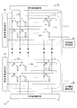
- FIG. 1 is an equivalent circuit diagram showing an overall electrical configuration of a liquid crystal display device according to an embodiment of the present invention. It is a figure which shows roughly the pixel electrode shape for every display area which concerns on one Embodiment of this invention.
- (A) in a figure is a chromaticity diagram which shows the chromaticity characteristic at the time of visually recognizing from the position of an elevation angle of 60 degrees with respect to the display surface of a display area
- (b) in the figure is a display surface of a display area.
- (c) in the figure is a view when viewed from a position at an elevation angle of 60 ° with respect to the display surface of the display area.
- (A) in a figure is a figure which shows schematically the shape of the pixel electrode which concerns on one Embodiment of this invention
- (b) in the figure shows the shape of the pixel electrode which concerns on one Embodiment of this invention. It is a figure shown roughly.
- (A) in a figure is a figure which shows schematically the shape of the pixel electrode which concerns on one Embodiment of this invention
- (b) in the figure shows the shape of the pixel electrode which concerns on one Embodiment of this invention. It is a figure shown roughly. It is a figure which shows the transmittance
- (A) in the figure is a diagram schematically showing a chromaticity state when the conventional liquid crystal display device is viewed vertically and obliquely, and (b) in the figure shows the conventional liquid crystal display device horizontally. It is a figure which shows roughly the state at the time of visually recognizing from diagonally.
- FIG. 2 is an equivalent circuit diagram showing the overall electrical configuration of the liquid crystal display device 20.
- the liquid crystal display device is a vertical alignment (VA) type liquid crystal display device in which liquid crystal molecules having negative dielectric anisotropy ( ⁇ ⁇ 0) are aligned perpendicularly to a substrate.
- the liquid crystal display device 20 includes a liquid crystal panel 12, signal line driving circuits 7a and 7b, and scanning line driving circuits 8a and 8b.
- the liquid crystal panel 12 has a display area 11a (first display area) and a display area 11b (second display area) described later. In the display area 11a, display is performed by a semi-transmissive method, and in the display area 11b, display is performed by a transmissive method or a semi-transmissive method.
- the liquid crystal panel 12 is configured by sandwiching a liquid crystal layer between a TFT substrate (not shown) and a counter substrate (not shown), and a plurality of pixels 10a arranged in a matrix. , 10b.
- the liquid crystal panel 12 includes pixel electrodes 1a and 1b, a signal line 2, a scanning line 3, and a thin film transistor (TFT) 4 on a TFT substrate.
- the counter electrode 5 and the counter electrode drive circuits 9a and 9b are provided on the counter substrate.
- Reference numeral 6 in the drawing denotes a liquid crystal cell, and the liquid crystal cell 6 is electrically treated as a capacitive element.
- one signal line 2 is formed in each column so as to be parallel to each other in the column direction (vertical direction), and the scanning lines 3 are parallel to each other in the row direction (horizontal direction). Thus, one is formed in each row.
- the plurality of signal lines 2 and the plurality of scanning lines 3 are arranged so as to cross each other, and a pixel 10a (first pixel) is formed at each intersection. That is, a region surrounded by two adjacent signal lines 2 and two adjacent scanning lines 3 is one pixel 10a.
- the pixel electrode 1a and the TFT 4 are formed corresponding to each pixel 10a.
- the source electrode of the TFT 4 is electrically connected to the signal line 2, and the gate electrode is electrically connected to the scanning line 3.
- the drain electrode is electrically connected to the pixel electrode 1a.
- the pixel electrode 1 a forms a liquid crystal capacitance with the counter electrode 5 through the liquid crystal cell 6.
- the gate of the TFT 4 is turned on by the scanning signal supplied from the scanning line driving circuit 8a to the scanning line 3, and the data signal supplied from the signal line driving circuit 7a to the signal line 2 is written into the pixel electrode 1a.
- 1a is set to a potential corresponding to the data signal.
- the counter electrode 5 is set to a predetermined potential by the counter electrode driving circuit 9a, and the liquid crystal cell 6 interposed between the pixel electrode 1a and the counter electrode 5 has a gradation display corresponding to the potential difference between the two electrodes. Can be realized.
- the plurality of signal lines 2 and the plurality of scanning lines 3 are arranged to intersect each other, and a pixel 10b (second pixel) is formed at each intersection.
- a pixel electrode 1b and a TFT 4 are also formed in each pixel 10b.
- the source electrode of the TFT 4 is electrically connected to the signal line 2, and the gate electrode is electrically connected to the scanning line 3.
- the drain electrode is electrically connected to the pixel electrode 1b.
- the pixel electrode 1 b forms a liquid crystal capacitance with the counter electrode 5 through the liquid crystal cell 6.
- the gate of the TFT 4 is turned on by the scanning signal supplied from the scanning line driving circuit 8b to the scanning line 3, and the data signal supplied from the signal line driving circuit 7b to the signal line 2 is written into the pixel electrode 1b.
- 1b is set to a potential corresponding to the data signal.
- the counter electrode 5 is set to a predetermined potential by the counter electrode drive circuit 9b, and the liquid crystal cell 6 interposed between the pixel electrode 1b and the counter electrode 5 has a gradation display corresponding to the potential difference between the two electrodes. Can be realized.
- the signal line 2 in the display area 11a is controlled by the signal line driving circuit 7a, and the scanning line 3 is controlled by the scanning line driving circuit 8a. Accordingly, the display area 11a is driven by the signal line driving circuit 7a and the scanning line driving circuit 8a.
- the signal line 2 in the display area 11b similarly, the signal line 2 is controlled by the signal line driving circuit 7b, and the scanning line 3 is controlled by the scanning line driving circuit 8b. Accordingly, the display area 11b is driven by the signal line driving circuit 7b and the scanning line driving circuit 8b.
- the display area 11a and the display area 11b according to the present embodiment can be driven independently.
- the configuration of the display area 11a and the display area 11b is not particularly limited.
- the liquid crystal display device 20a in which each pixel 10a in the display area 11a is provided with a memory circuit for storing image data may be used. .
- the image can be displayed with low power consumption without continuously supplying the image data from the outside.
- various wirings such as an in-pixel circuit driving wiring are provided together with the scanning lines 3.
- the detailed configuration is not mentioned.
- the liquid crystal display device 20 includes the display area 11a and the display area 11b.
- One is a display area 11a that performs display by a semi-transmissive method
- the other is a display area 11b that performs display by a transmissive or semi-transmissive method.
- the pixel electrode 1a includes a semi-transmissive electrode having a portion composed of an electrode that transmits backlight light and a portion composed of an electrode that reflects external light. Is used.
- the display region 11b when the display region 11b performs display by a transmission method, a transmission electrode that transmits light from the backlight is used as the pixel electrode 1b.
- the pixel electrode 1b when the display region 11b performs display by a transflective method, the pixel electrode 1b includes a portion configured by an electrode that transmits backlight light and a portion configured by an electrode that reflects external light. The transflective electrode is used.
- the configuration has a plurality of display areas as in this embodiment, the direction of the chromaticity change differs for each display area.
- the chromaticity of each display region differs depending on the viewing angle, and the display quality of the liquid crystal display device is degraded. Therefore, in the present embodiment, the shape of the pixel electrode 1a in the display area 11a or the pixel electrode 1b in the display area 11b is changed, and the direction of chromaticity change in the display area 11a and the direction of chromaticity change in the display area 11b Are the same. Thereby, it is possible to prevent the display quality of the liquid crystal display device 20 from deteriorating.
- the display area 11a adopts the semi-transmission method and the display area 11b adopts the transmission method will be described as an example.
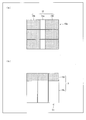
- the pixel electrode shape for each of the display areas 11a and 11b of the liquid crystal display device 20 in this case is schematically shown in FIG.
- the pixel electrode 1a in the display area 11a, the pixel electrode 1a has a transmissive electrode 15a formed of an electrode that transmits light from a backlight, and a reflective electrode 15b formed of an electrode that reflects external light.
- a transmissive electrode 15 is used in the display region 11b.
- the transmissive electrode 16 that transmits the light of the backlight is used as the pixel electrode 1b.
- the display area includes a plurality of display areas, and each display area includes electrodes of the same display method (that is, any one has the transmission electrode 16 and any one has the semi-transmission electrode 15 (transmission electrode).
- the shape of the electrode is changed.
- the transmissive electrode 15a of the semi-transmissive electrode 15 in the display region 11a and the transmissive electrode 16 of the display region 11b adopt the same transmission method.
- the transmission direction of the transflective electrode 15 or the display region 11b of the display region 11a is set so that the extending direction of the long side of the transmissive electrode 15a (hereinafter referred to as the long side direction) and the long side direction of the transmissive electrode 16 are the same.
- the shape of the electrode 16 is changed.
- the long side direction of the transmissive electrode 15 a and the long side direction of the transmissive electrode 16 coincide with each other.
- the direction of chromaticity change in the display area 11a is the same as the direction of chromaticity change in the display area 11b.
- the detailed mechanism will be described below.
- the transmittance characteristic of the liquid crystal display device is determined by the magnitude of retardation generated in the liquid crystal layer.
- the chromaticity characteristics of the liquid crystal display device are also determined by the magnitude of retardation generated in the liquid crystal layer.
- produces in a liquid-crystal layer in a liquid crystal display device differs. Therefore, a difference occurs between the transmittance characteristic in the front direction and the transmittance characteristic in the oblique direction.
- a factor that determines the size of retardation of the liquid crystal layer is the shape of the pixel electrode.
- the magnitude of the retardation of the liquid crystal layer varies depending on the shape of the pixel electrode. That is, in the display area 11a and the display area 11b in which the shapes of the pixel electrodes 1a and 1b are different, the direction of the chromaticity change is different. As a result, the chromaticity of each of the display areas 11a and 11b varies depending on the viewing angle, and the display quality of the liquid crystal display device 20 is degraded.
- FIG. 3 schematically shows pixel electrode shapes for the display regions 11a and 11b.
- the pixels 10a in the display area 11a are arranged with the semi-transmissive electrodes 15 as shown in (A)
- the pixels 10b in the display area 11b are arranged with the transmissive electrodes 16 as shown in (B).
- FIG. 4 shows the chromaticity characteristics when the semi-transmissive electrodes 15 are arranged as in (A).
- (A) in FIG. 4 is a chromaticity diagram showing chromaticity characteristics when viewed from a position at an elevation angle of 60 ° with respect to the display surface of the display region 11a.
- the chromaticity of the display screen changes to the yellow side.
- the chromaticity of the display screen changes to the blue side.
- FIG. (B) in FIG. 4 is a chromaticity diagram showing chromaticity characteristics when viewed from a position at an elevation angle of 60 ° with respect to the display surface of the display region 11b.
- the chromaticity of the display screen changes to the blue side.
- the display screen is viewed from the positions of azimuth angles of 135 ° and 315 °, the chromaticity of the display screen changes to the yellow side.
- the direction of change in chromaticity when viewed from the position is different and changes in opposite directions.
- the direction of chromaticity change when viewed from azimuth angles of 135 ° and 315 ° is also different and changes in opposite directions. That is, since the chromaticity change directions of the display area 11a and the display area 11b are different depending on the viewing angle, the color of either the display area 11a or the display area 11b is emphasized.
- the translucent electrodes 15 are arranged in the pixels 10a of the display region 11a as shown in FIG. Specifically, they are arranged so that the long side direction of the transmissive electrode 16 arranged as shown in (B) is the same as the long side direction of the transmissive electrode 15a of the pixel electrode 1a.
- the chromaticity characteristics when the semi-transmissive electrodes 15 are arranged as in (C) are shown in (c) of FIG. (C) in FIG. 4 is a chromaticity diagram showing chromaticity characteristics when viewed from a position at an elevation angle of 60 ° with respect to the display surface of the display area 11a.
- the chromaticity of the display screen changes to the blue side.
- the chromaticity of the display screen changes to the yellow side.
- the azimuth angles are 45 ° and 225 °.
- the direction of chromaticity change when viewed is the same.
- the direction of change in chromaticity when viewed from positions with azimuth angles of 135 ° and 315 ° is the same. That is, even when the display screen is viewed from an oblique direction, the chromaticity change directions of the display area 11a and the display area 11b are the same, so that the color of either the display area 11a or the display area 11b is not emphasized.
- the semi-transmissive method is adopted in the display region 11a and the semi-transmissive electrode 15 is composed of the transmissive electrode 15a and the reflective electrode 15b.
- the configuration is not necessarily limited thereto.
- the pixel electrode 1a including the semi-transmissive electrode 15 in which the transmissive electrode 15a is formed between the two reflective electrodes 15b can be used.
- An example of the shape of the pixel electrodes 1a and 1b in this case is shown in FIG. (A) in FIG. 5 is a diagram schematically showing the shape of the pixel electrode 1b (semi-transmissive electrode 15) in the pixel 10a of the display region 11a.
- (B) in FIG. 5 is a diagram schematically showing the shape of the pixel electrode 1b (transmission electrode 16) in the pixel 10b of the display region 11b.
- the long side direction of the transmissive electrode 16 of the pixel 10b extends in the vertical direction in the figure. Therefore, since the transmissive electrode 15a of the transflective electrode 15 of the pixel 10a adopts the same transmissive method as the transmissive electrode 16 of the pixel 10b, attention is paid to the long side direction of the transmissive electrode 15a as shown in FIG.
- the long side direction is arranged so as to coincide with the long side direction of the transmissive electrode 16 of the pixel 10b, that is, so as to extend in the vertical direction of the drawing.
- the long-side directions of the transmissive electrode 15a and the transmissive electrode 16 adopting the same transmissive method coincide with each other, so that the chromaticity change directions of the display region 11a and the display region 11b are the same.
- the color of either the display area 11a or the display area 11b is not emphasized, it is possible to prevent display quality from being deteriorated.
- the transflective method is adopted in the display area 11a and the transmissive method is adopted in the display area 11b.
- the present invention is not necessarily limited thereto.
- both the display area 11a and the display area 11b can cope with the case where the transflective method is adopted.
- An example of the shape of the pixel electrodes 1a and 1b in this case is shown in FIG.
- FIG. 6A schematically shows the shape of the pixel electrode 1a (semi-transmissive electrode 15) in the pixel 10a of the display area 11a.
- 6B is a diagram schematically showing the shape of the pixel electrode 1b (semi-transmissive electrode 15) in the pixel 10b of the display region 11b.
- the long side direction of the transmissive electrode 15a of the semi-transmissive electrode 15 in the pixel 10b extends in the vertical direction of the drawing. Therefore, since the transmissive electrode 15a of the pixel 10a adopts the same transmissive method as the transmissive electrode 15a of the pixel 10b, as shown in FIG. 6A, attention is paid to the long side direction of the transmissive electrode 15a of the pixel 10a.
- the long side direction is arranged so as to coincide with the long side direction of the transmissive electrode 15a of the pixel 10b, that is, so as to extend in the vertical direction of the drawing.
- the long-side directions of the transmissive electrode 15a of the pixel 10a and the transmissive electrode 15a of the pixel 10b coincide with each other, so that the chromaticity change directions of the display region 11a and the display region 11b are the same.
- the color of either the display area 11a or the display area 11b is not emphasized, it is possible to prevent display quality from being deteriorated.
- the direction in which the long side of the transmissive electrode 15a of the pixel 10a and the long side of the transmissive electrode 15a of the pixel 10b extend is not particularly limited. That is, there is no problem even if the long-side direction of the transmissive electrode 15a of the pixel 10a and the transmissive electrode 15a of the pixel 10b extends in the left-right direction of (a) and (b) in FIG. In this way, if the long-side direction of the transmissive electrode 15a of the pixel 10a and the transmissive electrode 15a of the pixel 10b coincide with each other, the long-side direction of both the transmissive electrodes 15a is either the vertical direction or the horizontal direction in the figure. Even if it extends in the direction, the effects of the present invention can be achieved.
- the present invention is not particularly limited thereto.
- a configuration having three or more display areas is also possible.
- the pixels 10a and 10b are assumed to be composed of three sub-pixels (red (R) pixel, green (G) pixel, and blue (B) pixel). Three are shown in an array. However, it is not necessarily limited to this.
- the pixel electrode 1a and the pixel electrode 1b have electrode portions that adopt the same display method (that is, one has the transmissive electrode 16 and the other has the semi-transmissive electrode 15 (the transmissive electrode 15a). ), Or both have a semi-transmissive electrode (transmissive electrode 15a)), but it goes without saying that the electrode portion is assumed to be rectangular. . That is, the case where the transmissive electrode 16 or the transmissive electrode 15a is square is not included.
- the liquid crystal display device is characterized in that for each of the second pixels, a part of the pixel electrode is constituted by the transmissive electrode.
- a region other than the transmissive electrode in the pixel electrode is configured by a reflective electrode that reflects light.
- a region of the pixel electrode other than the transmissive electrode is formed of a reflective electrode that reflects light.
- part of the pixel electrode is configured by the transmissive electrode in both the first pixel and the second pixel. That is, both the first pixel and the second pixel have a transflective electrode as a pixel electrode. Therefore, even when both the first display area and the second display area are displayed by the transflective method, the direction of chromaticity change in both display areas can be made uniform.
- the liquid crystal display device is characterized in that, for each of the second pixels, the pixel electrode is constituted by the transmissive electrode.
- the liquid crystal display device is characterized in that, for each of the first pixels, a region other than the transmissive electrode in the pixel electrode is configured by a reflective electrode that reflects light.
- the pixel electrode of the second pixel is configured by the transmissive electrode. That is, the first pixel includes a transflective electrode as a pixel electrode, and the second pixel includes a transmissive electrode as a pixel electrode. Therefore, even when the first display area displays by the transflective method and the second display area displays by the transmissive method, the direction of the chromaticity change in both display areas can be made uniform.
- the liquid crystal display device of the present invention can be suitably used for a display screen of an electronic device such as a personal computer, a mobile phone, a portable information terminal, a portable music player, or a digital camera.
Landscapes
- Physics & Mathematics (AREA)
- Nonlinear Science (AREA)
- Mathematical Physics (AREA)
- Chemical & Material Sciences (AREA)
- Crystallography & Structural Chemistry (AREA)
- General Physics & Mathematics (AREA)
- Optics & Photonics (AREA)
- Geometry (AREA)
- Liquid Crystal (AREA)
Abstract
本発明に係る液晶表示装置(20)は、表示領域(11a)および表示領域(11b)を有している。表示領域(11a)は、透過表示を行う透過電極(15a)と反射表示を行う反射電極(15b)とからなる半透過電極15を画素電極として備えた画素(10a)を有している。表示領域(11b)は透過表示を行う透過電極(16)を画素電極として備えた画素(10b)を有している。この際、画素(10a)の透過電極(15a)が有する長辺の伸展方向と、画素(10b)の透過電極(16)が有する長辺の伸展方向とが同じになるように配置されている。透過電極(15a)の長辺方向と、透過電極(16)の長辺方向とを揃えることによって、表示領域(11a)における色度変化の方向と、表示領域(11b)における色度変化の方向とが同じになる。
Description
本発明は、液晶表示装置に関し、特に、複数の表示領域を有する液晶表示装置に関する。
近年では、従来主流であったブラウン管を使用した表示装置から、薄型のフラットパネルディスプレイ(FPD)の表示装置が広く利用されるようになっている。FPDには、表示素子として液晶、発光ダイオード(LED)または、有機エレクトロルミネッセンス(有機EL)等を利用したものがある。中でも液晶を利用した表示装置は、薄型、軽量、および低消費電力という利点から、その研究開発が盛んに行われている。
液晶表示装置(LCD)の駆動には、薄膜トランジスタ(TFT)のアクティブマトリックス(AM)回路を利用した方式がある。AM回路とは、画素ごとに表示/非表示を制御するスイッチ回路である。AM回路は画素ごとに制御しているので、表示装置の配線数が増えても、各画素を確実に動作することができる。そのため、AM回路を利用した液晶表示装置では、高精細化、コントラストの明晰化、また反応速度の高速化が可能である。
従来の液晶表示装置では、表示パネルの裏面にバックライトを配置し、当該バックライトを点灯して透過表示を行う透過型のものが主流であった。しかし、透過型液晶表示装置以外にも、反射方式によって表示を行う液晶表示装置、および半透過方式によって表示を行う液晶表示装置等が開発されている。反射型表示装置では、装置内部に反射板を設けたり、外部からの入射光を反射するような反射電極を画素電極として用いたりすることによって、外光を反射して表示光源としている。また、半透過型液晶表示装置では、光を反射する反射部と、光を透過する透過部とを有する電極を画素電極として用いており、外光は反射部で反射し、バックライト光は透過部を通過する。したがって、半透過型表示装置は、明所では外光を光源とした表示を行い、暗所ではバックライト光を光源とした表示を行うことができる。一般的に、反射型液晶表示装置または半透過型液晶表示装置では、バックライトを省略、あるいはバックライトの点灯時間を軽減することができるので、表示装置の消費電力を抑えることができる。
最近では、表示装置の省電力化対策として、1つの表示画面を複数の表示領域に分割するという試みがなされている。例えば、特許文献1には、透過方式によって表示を行う表示領域と、半透過方式によって表示を行う表示領域とを有する表示画面を備えた液晶表示装置が開示されている。これによれば、透過方式によって表示を行う表示領域に画像を表示し、半透過方式によって表示を行う表示領域に文字を表示するというように、表示情報の種類等で表示領域を使い分けることによって、使用環境上の制約を緩和し、表示画像の視認性と消費電力の低減とを両立することが可能である。さらに本文献では、半透過方式によって表示を行う表示領域において、透過表示部に開口部を設けることによって、当該表示領域で透過方式によって表示を行う際の輝度向上を図っている。これによって、両表示領域の輝度差を低減して、違和感のない画像表示を行うことができる。
さて、従来の垂直配向モードの液晶表示装置では、表示画面を斜め方向から視認した際に、正面方向から視認した場合と比較して表示画像が白っぽく見えてしまう問題がある。これは、液晶層で発生するリタデーションの大きさが異なるためである。以下に、液晶層のリタデーションについて、図7を参照して詳しく説明する。図7は、従来の液晶表示装置における透過率特性を示す図である。本図では、横軸は液晶層への印加電圧(V)を示し、縦軸は光の透過率(%)を示す。なお、本図では、表示画面を正面方向から視認した際の透過率特性と、仰角60°の位置から表示画面を視認した際の透過率特性とを示している。
一般的に液晶表示装置では、液晶層に配向制御用構造物等を設けることによって、液晶分子が複数方向に配向するように制御している。具体的には、配向制御用構造物を境に液晶分子の配向方向が変化している。その結果、図7に示すように、表示画面を正面方向から視認した際の透過率特性(図中の記号◇)と、表示画面を斜め方向から視認した際の透過率特性(図中の記号△)とに誤差が生じる。より詳細には、斜め方向の透過率特性には、正面方向での透過率特性に比較して透過率が上昇する階調領域と、透過率が減少する階調領域とが存在している。その結果、斜め方向での透過率が正面方向での透過率より大きい領域では、暗い中間調の表示画像が白っぽく見えてしまう。
さらに、従来の液晶表示装置では、表示画面を正面方向から視認した際の色度特性と、表示画面を斜め方向から視認した際の色度特性とにおいても誤差が生じる。色度も液晶層に生じるリタデーションの大きさに依存して変化するため、視認する角度によって色度が変化してしまう現象が生じる。このため、正面方向での色度に対して斜め方向の色度が変化してしまうという問題が生じている。
特許文献2では、上記問題を解消するために、基板間に印加された電圧よりも低い実効電圧が液晶にかかる低実効電圧領域を一部に備え、当該低実効電圧領域と他の領域との間で閾値電圧が異なるように構成した液晶表示装置を開示している。これによれば、閾値電圧が異なる領域間において透過率特性が平均され、正面方向と斜め方向との透過率の差が小さくなる。したがって、正面方向と斜め方向との間における表示画像の色度ずれの少ない良好な階調視覚特性が得られる。
上記液晶層で発生するリタデーションの大きさを決定する因子として、液晶層内に設けられた配向制御用構造物、バスライン、または画素電極等のレイアウトが挙げられる。したがって、画素の構造によっては、個々の画素内にも液晶分子のリタデーションが発生し得る。上記した特許文献1に開示されている液晶表示装置のように、表示画面を複数の表示領域に分割している場合には、表示領域ごとに画素電極等の形状が異なるため、表示領域ごとの画素構造が異なる。その結果、このような液晶表示装置の表示画面の視認状態は図8に示すようになる。本図では色味の違いを塗り分けて表している。
図8中の(a)は、液晶表示装置40を縦にして斜め方向から視認した場合の色度状態を概略的に示す図である。本図に示すように、液晶表示装置40を斜め方向から視認した場合には、表示領域21aと表示領域21bとで色味が異なり、表示領域21aの色度変化が強調される。一方、図8中の(b)は、液晶表示装置40を横にして斜め方向から視認した場合の色度状態を概略的に示す図である。本図に示すように、液晶表示装置40を斜め方向から視認した場合には、表示領域21aと表示領域21bとで色味が異なり、表示領域21bの色度変化が強調される。
このように、表示領域ごとにその色度変化の方向が異なってくるため、視認する角度によって表示領域ごとの色度が異なり、液晶表示装置の表示品位が低下してしまう。上記特許文献2に開示されている技術では、1つの表示領域における色度変化を改善することはできるが、複数の表示領域においてそれぞれの領域で色度変化が生じている場合には対応することができない。
そこで、本発明は上記課題に鑑みてなされたものであり、その目的は、複数の表示領域を有する垂直配向型の液晶表示装置において、表示領域ごとに異なる色度変化による表示品位の低下を改善する液晶表示装置を提供することにある。
本発明に係る液晶表示装置は、上記課題を解決するために、複数の画素を有する垂直配向型の液晶表示装置において、上記画素ごとに、画素電極と、上記画素電極に対向する対向電極と、上記画素電極と上記対向電極との間に配置された液晶層とを備えた液晶表示装置であって、上記複数の画素として、複数の第1画素を含む第1表示領域と、上記複数の画素として、上記複数の第1画素とは異なる複数の第2画素を含む第2表示領域とを備え、上記第1画素ごとに、上記画素電極の一部が、光を透過する矩形の透過電極によって構成されており、上記第2画素ごとに、上記画素電極の少なくとも一部が、光を透過する矩形の透過電極によって構成されており、上記第1画素の上記透過電極が有する長辺の伸展方向と、上記第2画素の上記透過電極が有する上記長辺の伸展方向とが同じであることを特徴としている。
上記の構成によれば、透過表示を行う透過電極によって一部が構成された画素電極を第1画素は有しており、透過表示を行う透過電極によって少なくとも一部が構成された画素電極を第2画素は有している。さらに、当該第1画素の透過電極が有する長辺の伸展方向と、当該第2画素の透過電極が有する長辺の伸展方向とが同じになるように配置されている。
一般的に、複数の表示領域を備える液晶表示装置では、視認方向ごとに、各表示領域における液晶のリタデーションが異なる。この一因として、表示領域ごとの画素電極形状等の画素構造の違いが挙げられる。そのため、異なる画素構造を有する複数の表示領域では、表示領域ごとに液晶のリタデーションの大きさに違いが生じる。その結果、表示領域ごとに色度が変化してしまうため、液晶表示装置の表示品位に悪影響を及ぼす。
そこで、本発明では、第1画素の透過電極の長辺方向と、第2画素の透過電極の長辺方向とを揃えることによって、視認方向ごとの第1表示領域における液晶のリタデーションの分布と、第2表示領域における液晶のリタデーションの分布とが同じようになる。その結果、第1表示領域の色度変化の方向と、第2表示領域の色度変化の方向とが同じになり、表示画面を斜めから視認した場合でも、第1表示領域および第2表示領域のいずれかの色味が強調されることがない。そのため、表示画面全体として色度変化が強調されず、表示品位の低下を防ぐことができる。よって、良好な表示品位を有する液晶表示装置を提供することができる。
本発明の他の目的、特徴、および優れた点は、以下に示す記載によって十分分かるであろう。また、本発明の利点は、添付図面を参照した次の説明で明白になるであろう。
本発明では、第1画素の透過電極の長辺方向と、第2画素の透過電極の長辺方向とを揃えることによって、第1表示領域における液晶のリタデーションの分布と、第2表示領域における液晶のリタデーションの分布とが同じようになる。その結果、第1表示領域の色度変化の方向と、第2表示領域の色度変化の方向とが同じになり、表示画面を斜めから視認した場合でも、第1表示領域および第2表示領域のいずれかの色味が強調されることがない。そのため、表示画面全体として色度変化が強調されず、表示品位の低下を防ぐことができる。よって、良好な表示品位を有する液晶表示装置を提供することができる。
(液晶表示装置20の概要)
本発明の一実施形態について図面を参照して説明する。まず、本実施形態に係る液晶表示装置(LCD)の概要について、図2を参照して説明する。図2は、液晶表示装置20の全体の電気的構成を示す等価回路図である。
本発明の一実施形態について図面を参照して説明する。まず、本実施形態に係る液晶表示装置(LCD)の概要について、図2を参照して説明する。図2は、液晶表示装置20の全体の電気的構成を示す等価回路図である。
本実施形態に係る液晶表示装置は、負の誘電異方性(ε<0)を有する液晶分子を基板に対して垂直に配向させた垂直配向(VA;Vertical Alignment)型の液晶表示装置である。図2に示すように、液晶表示装置20は、液晶パネル12、信号線駆動回路7a,7b、および走査線駆動回路8a,8bを備えている。液晶パネル12は、後述する表示領域11a(第1表示領域)および表示領域11b(第2表示領域)を有している。表示領域11aでは、半透過方式によって表示を行い、表示領域11bでは、透過方式または半透過方式によって表示を行う。
具体的には、液晶パネル12は、TFT基板(図示せず)と対向基板(図示せず)との間に液晶層を挟持して構成されており、行列状に配列された複数の画素10a,10bを有している。そして、液晶パネル12は、TFT基板上に、画素電極1a,1b、信号線2、走査線3、および薄膜トランジスタ(TFT)4を備えている。また、対向基板上に対向電極5、および対向電極駆動回路9a,9bを備えている。図中の符号6は液晶セルを示し、液晶セル6は電気的には容量素子として扱われる。
表示領域11aでは、信号線2は、列方向(縦方向)に互いに平行となるように各列に1本ずつ形成されており、走査線3は、行方向(横方向)に互いに平行となるように各行に1本ずつ形成されている。複数の信号線2と複数の走査線3とは互いに交差するように配置されており、その交差点ごとに画素10a(第1画素)が形成されている。すなわち、隣り合う2つの信号線2と、隣り合う2つの走査線3とによって囲まれた領域が1つの画素10aである。画素電極1aおよびTFT4は、各画素10aに対応してそれぞれ形成されている。TFT4のソース電極が信号線2に電気的に接続されており、ゲート電極が走査線3に電気的に接続されている。また、ドレイン電極が画素電極1aに電気的に接続されている。なお、画素電極1aは、対向電極5との間に液晶セル6を介して液晶容量を形成している。
これにより、走査線駆動回路8aから走査線3に供給される走査信号によってTFT4のゲートをオンにし、信号線駆動回路7aから信号線2に供給されるデータ信号を画素電極1aに書き込んで画素電極1aを当該データ信号に応じた電位に設定する。そして、対向電極5は対向電極駆動回路9aによって所定の電位に設定されており、画素電極1aと対向電極5との間に介在する液晶セル6は、両電極間の電位差に応じた階調表示を実現することができる。
一方、表示領域11bについても同様に、複数の信号線2と複数の走査線3とは互いに交差するように配置されており、その交差点ごとに画素10b(第2画素)が形成されている。各画素10bにも、画素電極1bおよびTFT4がそれぞれ形成されている。TFT4のソース電極が信号線2に電気的に接続されており、ゲート電極が走査線3に電気的に接続されている。また、ドレイン電極が画素電極1bに電気的に接続されている。なお、画素電極1bは、対向電極5との間に液晶セル6を介して液晶容量を形成している。
これにより、走査線駆動回路8bから走査線3に供給される走査信号によってTFT4のゲートをオンにし、信号線駆動回路7bから信号線2に供給されるデータ信号を画素電極1bに書き込んで画素電極1bを当該データ信号に応じた電位に設定する。そして、対向電極5は対向電極駆動回路9bによって所定の電位に設定されており、画素電極1bと対向電極5との間に介在する液晶セル6は、両電極間の電位差に応じた階調表示を実現することができる。
上述したように、表示領域11aにおける信号線2は信号線駆動回路7aによって制御されており、走査線3は走査線駆動回路8aによって制御されている。したがって、表示領域11aは、信号線駆動回路7aおよび走査線駆動回路8aによって駆動される。一方、表示領域11bについても同様に、信号線2は信号線駆動回路7bによって制御されており、走査線3は走査線駆動回路8bによって制御されている。したがって、表示領域11bは、信号線駆動回路7bおよび走査線駆動回路8bによって駆動される。このように、本実施形態に係る表示領域11aおよび表示領域11bは、それぞれ独立して駆動することができる。
なお、表示領域11aおよび表示領域11bの構成には特に限定はなく、例えば、表示領域11aの各画素10aに、画像データを記憶するメモリ回路を設けた液晶表示装置20aにすることも可能である。メモリ回路に画像データを記憶(保持)させることによって、外部から画像データを供給し続けることなく画像を低消費電力で表示することができる。この場合は、画素内回路駆動用配線等の各種配線を走査線3と共に設ける。ここでは、その詳細な構成については言及しない。
(表示領域11aおよび表示領域11bの構成)
上述したように、液晶表示装置20は、表示領域11aおよび表示領域11bを有している。一方は、半透過方式によって表示を行う表示領域11aであり、他方は、透過方式または半透過方式によって表示を行う表示領域11bである。表示領域11aは半透過方式によって表示を行うので、画素電極1aとして、バックライトの光を透過する電極で構成された部分と、外光を反射する電極で構成された部分とを有する半透過電極を用いる。一方、表示領域11bが透過方式によって表示を行う場合には、画素電極1bとしてバックライトの光を透過する透過電極を用いる。また、表示領域11bが半透過方式によって表示を行う場合には、画素電極1bとして、バックライトの光を透過する電極で構成された部分と、外光を反射する電極で構成された部分とを有する半透過電極を用いる。
上述したように、液晶表示装置20は、表示領域11aおよび表示領域11bを有している。一方は、半透過方式によって表示を行う表示領域11aであり、他方は、透過方式または半透過方式によって表示を行う表示領域11bである。表示領域11aは半透過方式によって表示を行うので、画素電極1aとして、バックライトの光を透過する電極で構成された部分と、外光を反射する電極で構成された部分とを有する半透過電極を用いる。一方、表示領域11bが透過方式によって表示を行う場合には、画素電極1bとしてバックライトの光を透過する透過電極を用いる。また、表示領域11bが半透過方式によって表示を行う場合には、画素電極1bとして、バックライトの光を透過する電極で構成された部分と、外光を反射する電極で構成された部分とを有する半透過電極を用いる。
本実施形態のように、複数の表示領域を有する構成だと、表示領域ごとにその色度変化の方向が異なる。その結果、視認する角度によって表示領域ごとの色度が異なり、液晶表示装置の表示品位が低下してしまう。そこで、本実施形態では、表示領域11aの画素電極1aまたは表示領域11bの画素電極1bの形状を変え、表示領域11aでの色度変化の方向と、表示領域11bでの色度変化の方向とを同じにしている。これによって、液晶表示装置20の表示品位の低下を防ぐことができる。
具体的に、表示領域11aでは半透過方式を採り、表示領域11bでは透過方式を採った場合を例に挙げて説明する。この場合の液晶表示装置20が有する表示領域11a,11bごとの画素電極形状を図1に概略的に示す。図1に示すように、表示領域11aでは、画素電極1aとしてバックライトの光を透過する電極で構成された透過電極15aと、外光を反射する電極で構成された反射電極15bとを有する半透過電極15を用いる。また、表示領域11bでは、画素電極1bとしてバックライトの光を透過する透過電極16を用いる。
本実施形態では、複数の表示領域を有し、同表示方式の電極をそれぞれの表示領域で備えている場合(すなわち、いずれかが透過電極16を有し、いずれかが半透過電極15(透過電極15a)を有している場合、またはすべてが半透過電極15(透過電極15a)を有している場合)には、その電極の形状を変える。例えば、図1では、表示領域11aの半透過電極15の透過電極15aと、表示領域11bの透過電極16とは、同じ透過方式を採る。そこで、透過電極15aの長辺の伸展方向(以下、長辺方向という)と、透過電極16の長辺方向とが同じになるように、表示領域11aの半透過電極15または表示領域11bの透過電極16の形状を変える。図1では、透過電極15aの長辺方向と、透過電極16の長辺方向とが一致している。
上記の構成によれば、表示領域11aの色度変化の方向と、表示領域11bの色度変化の方向とが同じになる。その詳しいメカニズムについて以下に説明する。
(色度変化の方向の調整)
一般的に、液晶表示装置では、液晶層で発生するリタデーションの大きさによって、液晶表示装置の透過率特性が決まる。また、液晶表示装置の色度特性についても、液晶層で発生するリタデーションの大きさによって決まる。なお、液晶表示装置において液晶層で発生するリタデーションの大きさが異なる。そのため、正面方向での透過率特性と、斜め方向での透過率特性とに差が生じてしまう。また、正面方向での色度特性と、斜め方向での色度特性とについても差が生じてしまう。その結果、視認する角度によって色度が変化してしまい、液晶表示装置の表示品位に悪影響を及ぼす。
一般的に、液晶表示装置では、液晶層で発生するリタデーションの大きさによって、液晶表示装置の透過率特性が決まる。また、液晶表示装置の色度特性についても、液晶層で発生するリタデーションの大きさによって決まる。なお、液晶表示装置において液晶層で発生するリタデーションの大きさが異なる。そのため、正面方向での透過率特性と、斜め方向での透過率特性とに差が生じてしまう。また、正面方向での色度特性と、斜め方向での色度特性とについても差が生じてしまう。その結果、視認する角度によって色度が変化してしまい、液晶表示装置の表示品位に悪影響を及ぼす。
液晶層のリタデーションの大きさを決定する因子として、画素電極の形状が挙げられる。画素電極の形状によって、液晶層のリタデーションの大きさが変わってくる。すなわち、画素電極1a,1bの形状が異なる表示領域11aおよび表示領域11bでは、それぞれの色度変化の方向が異なってくる。その結果、視認する角度によって表示領域11a,11bごとの色度が異なり、液晶表示装置20の表示品位が低下してしまう。
図3に、表示領域11a,11bごとの画素電極形状を概略的に示す。図3に示すように、通常は、表示領域11aの画素10aは(A)のように半透過電極15を配列し、表示領域11bの画素10bは(B)のように透過電極16を配列する。ここで、(A)のように半透過電極15を配列した場合の色度特性を図4中の(a)に示す。図4中の(a)は、表示領域11aの表示面に対して仰角60°の位置から視認した場合の色度特性を示す色度図である。本図に示すように、方位角(phi)45°および225°の位置から表示画面を視認した場合には、表示画面の色度が黄色側に変化している。逆に、方位角135°および315°の位置から表示画面を視認した場合には、表示画面の色度が青色側に変化している。
一方、図3の(B)のように透過電極16を配列した場合の色度特性を図4中の(b)に示す。図4中の(b)は、表示領域11bの表示面に対して仰角60°の位置から視認した場合の色度特性を示す色度図である。本図に示すように、方位角45°および225°の位置から表示画面を視認した場合には、表示画面の色度が青色側に変化している。逆に、方位角135°および315°の位置から表示画面を視認した場合には、表示画面の色度が黄色側に変化している。
このように、図3の(A)のように半透過電極15を配列した表示領域11aと、(B)のように透過電極16を配列した表示領域11bとでは、方位角45°および225°の位置から視認した際の色度変化の方向が異なり、互いに逆方向に変化している。同様に、方位角135°および315°の位置から視認した際の色度変化の方向も異なり、互いに逆方向に変化している。すなわち、視認する角度によって表示領域11aおよび表示領域11bそれぞれの色度変化の方向が異なるので、表示領域11aおよび表示領域11bのいずれかの色味が強調されてしまう。これは、仰角60°の位置から視認した際の表示領域11aにおける液晶のリタデーションの分布と、表示領域11bにおける液晶のリタデーションの分布とが異なっているためである。その結果、表示画面全体の表示品位が低下してしまう。
ここで、本実施形態では、表示領域11aの画素10aは図3の(C)のように半透過電極15を配列している。具体的には、(B)のように配列した透過電極16の長辺方向と、画素電極1aの透過電極15aの長辺方向とが同じになるようにして配列している。(C)のように半透過電極15を配列した場合の色度特性を図4中の(c)に示す。図4中の(c)は、表示領域11aの表示面に対して仰角60°の位置から視認した場合の色度特性を示す色度図である。本図に示すように、方位角45°および225°の位置から表示画面を視認した場合には、表示画面の色度が青色側に変化している。逆に、方位角135°および315°の位置から視認した場合には、表示画面の色度が黄色側に変化している。
このように、(C)のように半透過電極15を配列した表示領域11aと、(B)のように透過電極16を配列した表示領域11bとでは、方位角45°および225°の位置から視認した際の色度変化の方向が同じになる。同様に、方位角135°および315°の位置から視認した際の色度変化の方向も同じになる。すなわち、表示画面を斜めから視認した場合でも、表示領域11aおよび表示領域11bの色度変化の方向が同じなので、表示領域11aおよび表示領域11bのいずれかの色味が強調されることがない。これは、透過電極16の長辺方向と、透過電極15aの長辺方向とを揃えることによって、表示領域11aにおける液晶のリタデーションの分布と、表示領域11bにおける液晶のリタデーションの分布とが同じようになるためである。そのため、表示画面全体として色度変化が強調されず、表示品位の低下を防ぐことができる。よって、良好な表示品位を有する液晶表示装置20を提供することが可能となる。
(画素電極1aの形状例)
以上で説明したように、本実施形態では、画素電極1aおよび画素電極1bで同表示方式の電極を備えている場合(すなわち、一方が透過電極16を有し、他方が半透過電極15(透過電極15a)を有している場合、または双方が半透過電極15(透過電極15a)を有している場合)には、その電極の形状を調整する。具体的には、同方式を採る電極部の長辺方向がそれぞれ同じになるようにする。
以上で説明したように、本実施形態では、画素電極1aおよび画素電極1bで同表示方式の電極を備えている場合(すなわち、一方が透過電極16を有し、他方が半透過電極15(透過電極15a)を有している場合、または双方が半透過電極15(透過電極15a)を有している場合)には、その電極の形状を調整する。具体的には、同方式を採る電極部の長辺方向がそれぞれ同じになるようにする。
以上では、表示領域11aにおいて半透過方式を採り、半透過電極15が透過電極15aと反射電極15bとからなる構成を例に挙げたが、必ずしもこれに限定されるわけではない。例えば、半透過方式を採る表示領域11aにおいて、2つの反射電極15bの間に透過電極15aが形成されている半透過電極15からなる画素電極1aでも対応可能である。この場合の画素電極1a,1bの形状例を図5に示す。図5中の(a)は、表示領域11aの画素10aにおける画素電極1b(半透過電極15)の形状を概略的に示す図である。図5中の(b)は、表示領域11bの画素10bにおける画素電極1b(透過電極16)の形状を概略的に示す図である。
図5中の(b)に示すように、画素10bの透過電極16の長辺方向は、図の上下方向に延びている。そこで、画素10aの半透過電極15の透過電極15aは、画素10bの透過電極16と同じ透過方式を採るので、図5中の(a)に示すように、透過電極15aの長辺方向に着目し、当該長辺方向が画素10bの透過電極16の長辺方向と一致するように、すなわち図の上下方向に伸展するように配置する。これによって、同じ透過方式を採る透過電極15aおよび透過電極16の長辺方向が一致するので、表示領域11aおよび表示領域11bの色度変化の方向が同じになる。その結果、表示領域11aおよび表示領域11bのいずれかの色味が強調されることがないため、表示品位の低下を防ぐことができる。
また、以上では、表示領域11aにおいて半透過方式を採り、表示領域11bにおいて透過方式を採る場合を示したが、必ずしもこれに限定されるわけではない。例えば、表示領域11aおよび表示領域11bいずれも半透過方式を採る場合にも対応可能である。この場合の画素電極1a,1bの形状例を図6に示す。図6中の(a)は、表示領域11aの画素10aにおける画素電極1a(半透過電極15)の形状を概略的に示す図である。図6中の(b)は、表示領域11bの画素10bにおける画素電極1b(半透過電極15)の形状を概略的に示す図である。
図6中の(b)に示すように、画素10bにおける半透過電極15の透過電極15aの長辺方向は、図の上下方向に延びている。そこで、画素10aの透過電極15aは、画素10bの透過電極15aと同じ透過方式を採るので、図6中の(a)に示すように、画素10aの透過電極15aの長辺方向に着目し、当該長辺方向が画素10bの透過電極15aの長辺方向と一致するように、すなわち図の上下方向に伸展するように配置する。これによって、画素10aの透過電極15aと、画素10bの透過電極15aとの長辺方向が一致するので、表示領域11aおよび表示領域11bの色度変化の方向が同じになる。その結果、表示領域11aおよび表示領域11bのいずれかの色味が強調されることがないため、表示品位の低下を防ぐことができる。
ところで、画素10aの透過電極15aの長辺と、画素10bの透過電極15aの長辺とが伸展する方向には、特に限定はない。すなわち、画素10aの透過電極15aと、画素10bの透過電極15aとの長辺方向が、図6中の(a)および(b)の左右方向に伸展していても問題はない。このように、画素10aの透過電極15aと、画素10bの透過電極15aとの長辺方向が一致していれば、両透過電極15aの長辺方向が、図の上下方向および左右方向のいずれの方向に伸展していても、本発明の効果を奏することができる。
なお、以上では、液晶表示装置20が表示領域11aおよび表示領域11bの2つの表示領域を有している場合を示したが、特にこれに限定されるものではない。例えば、3つ以上の表示領域を有する構成にすることも可能である。
また、本実施形態では、各画素10a,10bは、3つのサブ画素(赤色(R)画素、緑色(G)画素、青色(B)画素)からなることを想定して、画素10a,10bを3つ配列して図示した。しかしながら、必ずしもこれに限定されるわけではない。
ところで、本実施形態では、同表示方式を採る電極部を画素電極1aおよび画素電極1bで有している場合(すなわち、一方が透過電極16を有し、他方が半透過電極15(透過電極15a)を有している場合、または双方が半透過電極(透過電極15a)を有している場合)を想定しているが、当該電極部が矩形であることを前提にしているのは言うまでもない。すなわち、透過電極16または透過電極15aが正方形の場合は含まれない。
本発明は上述した実施形態に限定されるものではなく、請求項に示した範囲で種々の変更が可能である。すなわち、請求項に示した範囲で適宜変更した技術的手段を組み合わせて得られる実施形態についても本発明の技術的範囲に含まれる。
〔実施形態の総括〕
以上のように、本発明に係る液晶表示装置は、上記第2画素ごとに、上記画素電極の一部が、上記透過電極によって構成されていることを特徴としている。
以上のように、本発明に係る液晶表示装置は、上記第2画素ごとに、上記画素電極の一部が、上記透過電極によって構成されていることを特徴としている。
また、本発明に係る液晶表示装置は、上記第1画素ごとに、上記画素電極における上記透過電極以外の領域が、光を反射する反射電極によって構成されており、上記第2画素ごとに、上記画素電極における上記透過電極以外の領域が、光を反射する反射電極によって構成されていることを特徴としている。
上記の構成によれば、第1画素および第2画素共に画素電極の一部が透過電極によって構成されている。すなわち、第1画素および第2画素共に画素電極として半透過電極を備えている構成である。よって、第1表示領域および第2表示領域共に半透過方式によって表示を行う場合でも、両表示領域における色度変化の方向を揃えることができる。
また、本発明に係る液晶表示装置は、上記第2画素ごとに、上記画素電極が、上記透過電極によって構成されていることを特徴としている。
また、本発明に係る液晶表示装置は、上記第1画素ごとに、上記画素電極における上記透過電極以外の領域が、光を反射する反射電極によって構成されていることを特徴としている。
上記の構成によれば、第2画素の画素電極は透過電極によって構成されている。すなわち、第1画素は画素電極として半透過電極を備えており、第2画素は画素電極として透過電極を備えている構成である。よって、第1表示領域が半透過方式によって表示を行い、第2表示領域が透過方式によって表示を行う場合でも、両表示領域における色度変化の方向を揃えることができる。
発明の詳細な説明の項においてなされた具体的な実施形態または実施例は、あくまでも、本発明の技術内容を明らかにするものであって、そのような具体例にのみ限定して狭義に解釈されるべきものではなく、本発明の精神と次に記載する請求の範囲内で、いろいろと変更して実施することができるものである。
本発明の液晶表示装置は、パーソナルコンピュータ、携帯電話、携帯情報端末、携帯音楽再生機、またはデジタルカメラ等の電子機器の表示画面に好適に用いることができる。
1a,1b 画素電極
2 信号線
3 走査線
4 薄膜トランジスタ
5 対向電極
6 液晶セル
7a,7b 信号線駆動回路
8a,8b 走査線駆動回路
9a,9b 対向電極駆動回路
10a,10b 画素
11a,11b,21a,21b表示領域
12 液晶パネル
14 メモリ回路
15 半透過電極
15a 透過電極
15b 反射電極
16 透過電極
20,20a,40 液晶表示装置
2 信号線
3 走査線
4 薄膜トランジスタ
5 対向電極
6 液晶セル
7a,7b 信号線駆動回路
8a,8b 走査線駆動回路
9a,9b 対向電極駆動回路
10a,10b 画素
11a,11b,21a,21b表示領域
12 液晶パネル
14 メモリ回路
15 半透過電極
15a 透過電極
15b 反射電極
16 透過電極
20,20a,40 液晶表示装置
Claims (5)
- 複数の画素を有する垂直配向型の液晶表示装置において、
上記画素ごとに、画素電極と、上記画素電極に対向する対向電極と、上記画素電極と上記対向電極との間に配置された液晶層とを備えた液晶表示装置であって、
上記複数の画素として、複数の第1画素を含む第1表示領域と、
上記複数の画素として、上記複数の第1画素とは異なる複数の第2画素を含む第2表示領域とを備え、
上記第1画素ごとに、上記画素電極の一部が、光を透過する矩形の透過電極によって構成されており、
上記第2画素ごとに、上記画素電極の少なくとも一部が、光を透過する矩形の透過電極によって構成されており、
上記第1画素の上記透過電極が有する長辺の伸展方向と、上記第2画素の上記透過電極が有する上記長辺の伸展方向とが同じであることを特徴とする液晶表示装置。 - 上記第2画素ごとに、上記画素電極の一部が、上記透過電極によって構成されていることを特徴とする請求項1に記載の液晶表示装置。
- 上記第2画素ごとに、上記画素電極が、上記透過電極によって構成されていることを特徴とする請求項1に記載の液晶表示装置。
- 上記第1画素ごとに、上記画素電極における上記透過電極以外の領域が、光を反射する反射電極によって構成されており、
上記第2画素ごとに、上記画素電極における上記透過電極以外の領域が、光を反射する反射電極によって構成されていることを特徴とする請求項2に記載の液晶表示装置。 - 上記第1画素ごとに、上記画素電極における上記透過電極以外の領域が、光を反射する反射電極によって構成されていることを特徴とする請求項3に記載の液晶表示装置。
Priority Applications (1)
| Application Number | Priority Date | Filing Date | Title |
|---|---|---|---|
| US13/639,245 US20130027650A1 (en) | 2010-04-05 | 2011-03-16 | Liquid crystal display device |
Applications Claiming Priority (2)
| Application Number | Priority Date | Filing Date | Title |
|---|---|---|---|
| JP2010-087185 | 2010-04-05 | ||
| JP2010087185 | 2010-04-05 |
Publications (1)
| Publication Number | Publication Date |
|---|---|
| WO2011125444A1 true WO2011125444A1 (ja) | 2011-10-13 |
Family
ID=44762404
Family Applications (1)
| Application Number | Title | Priority Date | Filing Date |
|---|---|---|---|
| PCT/JP2011/056303 Ceased WO2011125444A1 (ja) | 2010-04-05 | 2011-03-16 | 液晶表示装置 |
Country Status (2)
| Country | Link |
|---|---|
| US (1) | US20130027650A1 (ja) |
| WO (1) | WO2011125444A1 (ja) |
Families Citing this family (1)
| Publication number | Priority date | Publication date | Assignee | Title |
|---|---|---|---|---|
| TWI554808B (zh) * | 2015-04-13 | 2016-10-21 | 友達光電股份有限公司 | 液晶顯示面板及液晶顯示器 |
Citations (4)
| Publication number | Priority date | Publication date | Assignee | Title |
|---|---|---|---|---|
| JP2001265295A (ja) * | 2000-03-23 | 2001-09-28 | Matsushita Electric Ind Co Ltd | 液晶表示装置及び情報携帯機器 |
| JP2002148604A (ja) * | 2000-11-07 | 2002-05-22 | Matsushita Electric Ind Co Ltd | 液晶表示装置およびそれを用いた携帯型情報通信装置 |
| JP2006189499A (ja) * | 2004-12-28 | 2006-07-20 | Toshiba Matsushita Display Technology Co Ltd | 液晶表示装置 |
| JP2008116603A (ja) * | 2006-11-02 | 2008-05-22 | Epson Imaging Devices Corp | 液晶表示パネル |
Family Cites Families (2)
| Publication number | Priority date | Publication date | Assignee | Title |
|---|---|---|---|---|
| JP3900123B2 (ja) * | 2003-07-30 | 2007-04-04 | セイコーエプソン株式会社 | 液晶表示装置、及び電子機器 |
| US8243237B2 (en) * | 2006-11-07 | 2012-08-14 | Sony Mobile Communications Ab | Transmissive and transflective device display |
-
2011
- 2011-03-16 US US13/639,245 patent/US20130027650A1/en not_active Abandoned
- 2011-03-16 WO PCT/JP2011/056303 patent/WO2011125444A1/ja not_active Ceased
Patent Citations (4)
| Publication number | Priority date | Publication date | Assignee | Title |
|---|---|---|---|---|
| JP2001265295A (ja) * | 2000-03-23 | 2001-09-28 | Matsushita Electric Ind Co Ltd | 液晶表示装置及び情報携帯機器 |
| JP2002148604A (ja) * | 2000-11-07 | 2002-05-22 | Matsushita Electric Ind Co Ltd | 液晶表示装置およびそれを用いた携帯型情報通信装置 |
| JP2006189499A (ja) * | 2004-12-28 | 2006-07-20 | Toshiba Matsushita Display Technology Co Ltd | 液晶表示装置 |
| JP2008116603A (ja) * | 2006-11-02 | 2008-05-22 | Epson Imaging Devices Corp | 液晶表示パネル |
Also Published As
| Publication number | Publication date |
|---|---|
| US20130027650A1 (en) | 2013-01-31 |
Similar Documents
| Publication | Publication Date | Title |
|---|---|---|
| JP4572854B2 (ja) | 液晶装置及び電子機器 | |
| JP4717672B2 (ja) | 液晶装置及び電子機器 | |
| JP5623982B2 (ja) | 半透過型表示装置及び電子機器 | |
| JP4956786B2 (ja) | 画像表示システム | |
| US11183132B2 (en) | Display device | |
| CN100520505C (zh) | 四色液晶显示器 | |
| KR20170107127A (ko) | 액정 표시 장치 | |
| US20160139462A1 (en) | Curved liquid crystal display | |
| JP2007140089A (ja) | 液晶表示装置 | |
| KR100823771B1 (ko) | 전기 광학 장치 및 전자기기 | |
| JP2010250265A (ja) | 液晶表示装置および電子機器 | |
| US20190130854A1 (en) | Display device | |
| JP2007094089A (ja) | 電気光学装置及び電子機器 | |
| US10976590B2 (en) | Liquid crystal display device | |
| US20070109453A1 (en) | Electro-optical apparatus and electronic apparatus | |
| WO2011125444A1 (ja) | 液晶表示装置 | |
| JP2023084047A (ja) | 表示装置 | |
| JP2024074484A (ja) | 液晶表示装置 | |
| JP2007094025A (ja) | 電気光学装置及び電子機器 | |
| CN116224645B (zh) | 显示装置 | |
| CN213815330U (zh) | 显示装置 | |
| JP2007094029A (ja) | 電気光学装置及び電子機器 | |
| JP2023084046A (ja) | 表示装置 | |
| JP2025006135A (ja) | 液晶表示装置 | |
| KR20080021381A (ko) | 액정표시소자 |
Legal Events
| Date | Code | Title | Description |
|---|---|---|---|
| 121 | Ep: the epo has been informed by wipo that ep was designated in this application |
Ref document number: 11765346 Country of ref document: EP Kind code of ref document: A1 |
|
| WWE | Wipo information: entry into national phase |
Ref document number: 13639245 Country of ref document: US |
|
| NENP | Non-entry into the national phase |
Ref country code: DE |
|
| 122 | Ep: pct application non-entry in european phase |
Ref document number: 11765346 Country of ref document: EP Kind code of ref document: A1 |
|
| NENP | Non-entry into the national phase |
Ref country code: JP |