WO2011125420A1 - 周辺露光装置および周辺露光方法 - Google Patents
周辺露光装置および周辺露光方法 Download PDFInfo
- Publication number
- WO2011125420A1 WO2011125420A1 PCT/JP2011/055875 JP2011055875W WO2011125420A1 WO 2011125420 A1 WO2011125420 A1 WO 2011125420A1 JP 2011055875 W JP2011055875 W JP 2011055875W WO 2011125420 A1 WO2011125420 A1 WO 2011125420A1
- Authority
- WO
- WIPO (PCT)
- Prior art keywords
- exposure
- light
- area
- peripheral
- exposed
- Prior art date
- Legal status (The legal status is an assumption and is not a legal conclusion. Google has not performed a legal analysis and makes no representation as to the accuracy of the status listed.)
- Ceased
Links
Images




Classifications
-
- G—PHYSICS
- G03—PHOTOGRAPHY; CINEMATOGRAPHY; ANALOGOUS TECHNIQUES USING WAVES OTHER THAN OPTICAL WAVES; ELECTROGRAPHY; HOLOGRAPHY
- G03F—PHOTOMECHANICAL PRODUCTION OF TEXTURED OR PATTERNED SURFACES, e.g. FOR PRINTING, FOR PROCESSING OF SEMICONDUCTOR DEVICES; MATERIALS THEREFOR; ORIGINALS THEREFOR; APPARATUS SPECIALLY ADAPTED THEREFOR
- G03F7/00—Photomechanical, e.g. photolithographic, production of textured or patterned surfaces, e.g. printing surfaces; Materials therefor, e.g. comprising photoresists; Apparatus specially adapted therefor
- G03F7/20—Exposure; Apparatus therefor
- G03F7/2022—Multi-step exposure, e.g. hybrid; backside exposure; blanket exposure, e.g. for image reversal; edge exposure, e.g. for edge bead removal; corrective exposure
- G03F7/2026—Multi-step exposure, e.g. hybrid; backside exposure; blanket exposure, e.g. for image reversal; edge exposure, e.g. for edge bead removal; corrective exposure for the removal of unwanted material, e.g. image or background correction
- G03F7/2028—Multi-step exposure, e.g. hybrid; backside exposure; blanket exposure, e.g. for image reversal; edge exposure, e.g. for edge bead removal; corrective exposure for the removal of unwanted material, e.g. image or background correction of an edge bead on wafers
-
- G—PHYSICS
- G03—PHOTOGRAPHY; CINEMATOGRAPHY; ANALOGOUS TECHNIQUES USING WAVES OTHER THAN OPTICAL WAVES; ELECTROGRAPHY; HOLOGRAPHY
- G03F—PHOTOMECHANICAL PRODUCTION OF TEXTURED OR PATTERNED SURFACES, e.g. FOR PRINTING, FOR PROCESSING OF SEMICONDUCTOR DEVICES; MATERIALS THEREFOR; ORIGINALS THEREFOR; APPARATUS SPECIALLY ADAPTED THEREFOR
- G03F7/00—Photomechanical, e.g. photolithographic, production of textured or patterned surfaces, e.g. printing surfaces; Materials therefor, e.g. comprising photoresists; Apparatus specially adapted therefor
- G03F7/70—Microphotolithographic exposure; Apparatus therefor
- G03F7/70383—Direct write, i.e. pattern is written directly without the use of a mask by one or multiple beams
- G03F7/70391—Addressable array sources specially adapted to produce patterns, e.g. addressable LED arrays
Definitions
- the present invention relates to a peripheral exposure apparatus and a peripheral exposure method for exposing a predetermined peripheral position of an exposure object such as a glass substrate for liquid crystal, a semiconductor wafer, and a photosensitive film.
- a resist is applied to the entire surface of the substrate, and a wiring pattern is manufactured by patterning into a desired shape by photolithography.
- the exposure position of the mask pattern is usually determined so that a strip-shaped blank having a width of about several millimeters is produced in the peripheral portion of the substrate.
- Patent Document 1 an apparatus described in Patent Document 1 is known as a peripheral exposure apparatus for a square substrate.
- the peripheral portion of the exposure object is continuously exposed, but a part of the peripheral exposure region may be left as a non-exposure region. This is because a pattern such as an identification code is formed in the non-exposed area before and after that.
- the identification code is used for history management and quality control for improving the yield of each process and the entire production line.
- the present invention has been made in view of the above problems, and provides a peripheral exposure apparatus and a peripheral exposure method capable of forming an exposure region including a non-exposed portion with a simple mechanism and a short processing time. It is aimed.
- a peripheral exposure apparatus is a peripheral exposure apparatus for exposing the periphery of an exposure object, and includes a light source, a moving device, and a control unit.
- the light source has a plurality of light emitting elements arranged in the width direction orthogonal to the direction of relative movement with the exposure object.
- the moving device relatively moves the light source and the exposure object.
- the control unit controls the light emission states of the plurality of light emitting elements during the relative movement.
- the controller turns on the plurality of light emitting elements to expose the exposure object.
- control unit turns off the non-exposure light-emitting element corresponding to the non-exposure area among the plurality of light-emitting elements in order to form the non-exposure area in the exposure area during the exposure operation.
- the non-exposure light-emitting element is turned off during the exposure operation, whereby a non-exposure area is formed in the exposure area. Therefore, the exposure area and the non-exposure area can be formed without slowing the relative movement speed of the light source and the exposure object. In this way, the peripheral exposure is performed in a short time by a simple mechanism.
- the control unit may turn off the non-exposure light-emitting element when the light source reaches the non-exposure area, and turn on the non-exposure light-emitting element when the light source moves away from the non-exposure area.
- the light-emitting element for turning off during non-exposure is turned on.
- the control unit may increase the illuminance of the light-emitting element for turning off during non-exposure more than other light-emitting elements when exposing the area other than the non-exposed area.
- sufficient exposure is performed on both sides of the non-exposure area in the relative movement direction. Therefore, the quality of the boundary in the scanning direction is improved.
- the control unit emits light for turning off during non-exposure more than other light emitting elements only when the light source is in a predetermined area adjacent to both sides in the relative movement direction of the non-exposure area when the area other than the non-exposure area is exposed.
- the illuminance of the element may be increased.
- the illuminance of the light emitting element for turning off during non-exposure is high only when the light source is in a predetermined area adjacent to both sides in the relative movement direction of the non-exposure area. A region that affects the exposure by increasing the illuminance of the light-emitting element for turning off the light is limited.
- the control unit may increase the illuminance of the non-exposure light-emitting element by 1.2 to 1.8 times higher than other light-emitting elements when exposing the area other than the non-exposed area.
- the non-exposure light-emitting element may be disposed in a middle portion in the width direction orthogonal to the direction of relative movement with the exposure object among the plurality of light-emitting elements.
- the non-exposure light-emitting element may be disposed at the end in the width direction orthogonal to the direction of relative movement with the exposure object among the plurality of light-emitting elements.
- a peripheral exposure method is a method for exposing the periphery of an exposure object.
- This method is a peripheral exposure apparatus including a light source having a plurality of light emitting elements arranged in a width direction orthogonal to a direction of relative movement with an exposure object, and a moving device for moving the light source and the exposure object relative to each other. used.
- the peripheral exposure method includes the following steps. ⁇ First exposure step in which an exposure operation is performed while all the light emitting elements are turned on in order to expose the object to be exposed. ⁇ For non-exposure light extinction among a plurality of light emitting elements to form a non-exposure area in the exposure area.
- Second exposure step of performing an exposure operation with the light emitting element turned off the non-exposure light emitting element is turned off during the exposure operation, thereby forming a non-exposure area in the exposure area. Therefore, the exposure area and the non-exposure area can be formed without slowing the relative movement speed of the light source and the exposure object. In this way, the peripheral exposure is performed in a short time by a simple mechanism.
- the first exposure step may be executed before and after the second exposure step.
- the first exposure step may include a third exposure step in which the illuminance of the non-exposure light emitting element is made higher than that of the other light emitting elements when an area other than the non-exposed area is exposed.
- a third exposure step in which the illuminance of the non-exposure light emitting element is made higher than that of the other light emitting elements when an area other than the non-exposed area is exposed.
- the third exposure step may be executed only when the light source is in a predetermined area adjacent to both sides in the relative movement direction of the non-exposure area.
- the illuminance of the light emitting element for turning off during non-exposure is high only when the light source is in a predetermined area adjacent to both sides in the relative movement direction of the non-exposure area.
- a region that affects the exposure by increasing the illuminance of the light-emitting element for turning off the light is limited. This is particularly noticeable when the non-exposure area is exposed at the end face in the width direction of the exposure area, that is, when the non-exposure light-emitting element is disposed at the end of the exposure head in the width direction. An effect is obtained.
- the illuminance of the non-exposure light-emitting element may be 1.2 to 1.8 times that of other light-emitting elements when the non-exposed area is exposed.
- a recording medium stores a program for causing a computer to execute the peripheral exposure method described above.
- an exposure region including a non-exposed portion can be formed with a simple mechanism and a short processing time.
- 1 is a perspective view schematically showing an embodiment of a peripheral exposure apparatus of the present invention. It is the schematic and side view which show the light source for edge exposure which arranged the light emitting diode in the grid
- a peripheral exposure apparatus is an apparatus (for example, the peripheral exposure apparatus 1) for exposing the periphery of an exposure object, and includes a light source (for example, the exposure head 4) and a moving apparatus (for example, XY stage 2) and a control unit (for example, control device 23).
- the light source has a plurality of light emitting elements (for example, light emitting diodes 13) arranged in a width direction (for example, Y direction) orthogonal to a direction (for example, X direction) that moves relative to the exposure object (for example, substrate S).
- the moving device relatively moves the light source and the exposure object.
- the control unit controls the light emission states of the plurality of light emitting elements during the relative movement.
- the controller turns on the plurality of light emitting elements to expose the object to be exposed, and forms a non-exposure area in the exposure area during the exposure operation.
- the light emitting element for turning off during exposure (for example, the second row portion 13b) is turned off.
- the non-exposure light-emitting element is turned off during the exposure operation, whereby a non-exposure area (for example, the non-exposure area 32) is formed in the exposure area. Therefore, the exposure area and the non-exposure area can be formed without slowing the relative movement speed of the light source and the exposure object. In this way, the peripheral exposure is performed in a short time by a simple mechanism.
- FIG. 1 is a perspective view schematically showing an embodiment of a peripheral exposure apparatus.
- the peripheral exposure apparatus 1 is applied to peripheral exposure of a liquid crystal panel, for example.
- the peripheral exposure apparatus 1 has an XY stage 2 that supports a substrate S coated with a resist, and a rotary table 3 that supports the XY stage 2.
- the peripheral exposure apparatus 1 further includes an exposure head 4 that performs peripheral exposure on the substrate S and a slider 5 that holds the exposure head 4.
- the peripheral exposure apparatus 1 further includes an illuminance meter 6 that detects the output light intensity of the exposure head 4, a DC power source 7 that supplies a drive current to the exposure head 4, and a temperature control mechanism 8 that controls the temperature of the exposure head 4. have.
- Examples of the substrate S include a glass substrate, a substrate made of another material, a semiconductor wafer, and a film. Various shapes can be used.
- the XY stage 2 moves the substrate S two-dimensionally.
- the XY stage 2 can move the substrate S in the X direction.
- the turntable 3 rotates the substrate S together with the XY stage 2.
- the exposure head 4 will be described with reference to FIG. 2A and 2B are a schematic view and a side view showing a peripheral exposure light source in which light emitting diodes are arranged in a grid of 5 rows and 5 columns.
- the exposure head 4 includes a rectangular base 11, a plurality of light emitting diodes 13, and a plurality of optical system members 15.
- the base 11 is a member that holds the plurality of light emitting diodes 13 and is a substantially square plate-like member.
- the plurality of light emitting diodes 13 are provided on the lower surface of the base 11 and can emit ultraviolet rays downward.
- the plurality of light emitting diodes 13 are arranged in a state of being aligned vertically and horizontally. In FIG.
- the light emitting diodes 13 are arranged in 5 ⁇ 5, but actually, for example, they are arranged in 17 ⁇ 17 squares at 17 ⁇ 17.
- the optical system member 15 is disposed below the light emitting diode 13. The ultraviolet rays emitted from the light emitting diode 13 are prevented from spreading by passing through the optical system member 15. Thereby, the dimensional accuracy of an exposure area can be improved.
- the slider 5 reciprocates the exposure head 4 in the Y direction (perpendicular to the X direction).
- the illuminometer 6 receives the output light of the exposure head 4 at the movement limit position of the exposure head 4 by the slider 5, and supplies an intensity detection signal to the DC power source 7.
- the DC power source 7 has a power source body 21 that supplies a driving voltage or current to the exposure head 4 and a control device 23 so that a predetermined output light intensity can be obtained.
- the control device 23 is a computer or a programmable logic array having an input function, a storage function, a comparison operation function, an operation command function, and the like.
- the control device 23 controls the driving voltage or current so that the light emitting diode 13 emits light only during exposure, and changes the exposure conditions as necessary.
- the control device 23 stores drive voltage or current data for each product type in advance in order to perform the above control.
- the control device 23 has a CPU 23a and a memory 23b.
- the memory 23b is a recording medium that stores a control program.
- a position signal is input to the control device 23 from the XY stage 2 and the slider 5 in order to inform the position of the exposure head 4 with respect to the substrate S.
- the temperature control mechanism 8 includes a chiller 8a for generating cooling water and a cooling water flow for supplying the cooling water to a bracket (not shown) of the exposure head 4 to cool the light emitting diode 13 and returning it to the chiller 8a again. It has a path 8b.
- the temperature control mechanism 8 further includes a valve 8c, a flow meter 8d, a water pressure meter 8e, and a water temperature sensor 8f provided at predetermined positions of the cooling water channel 8b along the cooling water channel 8b.
- the water temperature sensor 8f is provided immediately downstream of the bracket (not shown) and supplies a temperature detection signal to the chiller 8a to control the operation of the chiller 8a.
- loading and unloading of the substrate S is performed by a substrate transfer robot (not shown), a shuttle transport transfer mechanism, a roller conveyor, or the like, or manually performed by an operator.
- an L-shaped alignment guide (not shown) or a pin-shaped guide that contacts only three L-shaped points.
- the substrate S coated with a resist is carried into the peripheral exposure apparatus 1.
- the XY stage 2 and the rotary table 3 are driven to position the substrate S.
- the exposure head 4 is directly opposed to the peripheral position to be exposed by the slider 5. Thus, the preparation for peripheral exposure is completed.
- the substrate S is moved in the X direction by the XY stage 2 and the exposure head 4 is operated by the DC power source 7, thereby exposing unnecessary peripheral resist along one side of the substrate S.
- the XY stage 2 and the rotary table 3 are operated, and the slider 5 is operated, so that the exposure head 4 faces the peripheral position to be exposed on the other side. Then, the unnecessary resist in the peripheral portion is exposed along the corresponding side of the substrate S. Similarly, the unnecessary resist in the peripheral portion is exposed along all the sides of the substrate S.
- peripheral exposure of all four sides of the rectangular substrate S can be performed, but only one of the sides may be exposed.
- the exposure head 4 on the entire shape to be exposed in advance or a shape obtained by dividing the shape, and irradiate with exposure for a necessary time while the stage is stationary.
- FIG. 3 is a control flowchart of the exposure operation in the first embodiment.
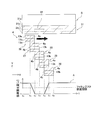
- FIG. 4 is a diagram showing the position and state of the light source with respect to the time axis, the exposure state of the exposure object, and the integrated exposure amount in the first embodiment.
- the horizontal direction in the figure is the X direction
- the operation of the exposure head 4 moving to the right side of the figure with respect to the substrate S will be described. Therefore, the right side of the drawing is referred to as “front side” and the left side of the drawing is referred to as “rear side”.
- the direction orthogonal to the X direction is defined as the Y direction.
- the light emitting diode 13 of the exposure head 4 is divided into a first row portion 13a, a second row portion 13b, and a third row portion 13c in the Y direction.
- Each part is composed of one or a plurality of rows of light emitting diodes 13.
- the exposure region 31 is a region extending in the X direction while having a predetermined width in the Y direction. That is, the longitudinal direction of the exposure region 31 is the X direction, and the lateral direction or the width direction is the Y direction.
- the exposure area 31c is divided.
- a portion where the identification code is marked first is defined as a non-exposure region 32.
- the horizontal axis of the graph is time, but the relative speed between the exposure head 4 and the substrate S is constant, so it may be considered as the movement distance.
- t0 is a relative movement start point
- t1, t2, t3, t4, t5, and t6 are equally spaced.
- two times correspond to the relative length of the exposure head 4. 4 shows a state in which the exposure head 4 is at the first position 26, the second position 27, the third position 28, the fourth position 29, and the fifth position 30 with respect to the substrate S.
- FIG. At the first position 26, the tip 4a of the exposure head 4 corresponds to t2.
- the front end 4a of the exposure head 4 corresponds to t3, and the rear end 4b of the exposure head 4 corresponds to t1.
- the front end 4a of the exposure head 4 corresponds to t4, and the rear end 4b of the exposure head 4 corresponds to t2.
- the front end 4a of the exposure head 4 corresponds to t5, and the rear end 4b of the exposure head 4 corresponds to t3.
- the front end 4a of the exposure head 4 corresponds to t6, and the rear end 4b of the exposure head 4 corresponds to t4.
- step S1 the DC power source 7 lights the exposure head 4. At this time, all the light emitting diodes 13 are turned on. Specifically, the control device 23 transmits a drive signal to the power source body 21, and for example, a voltage is applied from the power source body 21 to the exposure head 4.
- step S2 the XY stage 2 starts an operation of moving the substrate S with respect to the exposure head 4 in the X direction. Thereafter, the substrate S continues to move relative to the exposure head 4 at a constant speed (first exposure step).
- first exposure step it is assumed that the exposure head 4 moves relative to the substrate S in the X direction front side (right side in the figure).
- step S3 the exposure head 4 reaches the non-exposure position, specifically, the tip 4a end of the exposure head 4 reaches the non-exposure region start position (t2). Wait for position 1 to arrive.
- step S4 the second row portion 13b of the exposure head 4 is turned off (hereinafter referred to as a second exposure step).
- step S5 the exposure head 4 leaves the non-exposure area. Specifically, the rear end 4b of the exposure head 4 reaches the non-exposure area end position (t4), that is, the exposure head 4 is the fifth in FIG. Wait for position 30 to be reached.
- step S6 the second row portion 13b of the exposure head 4 is turned on. That is, when the light source moves away from the non-exposure area, the non-exposure light-emitting element is turned on, so that the non-exposure light-emitting element is exposed in the non-exposure area.
- step S7 the process waits for the exposure head 4 to reach the end of the exposure area of the substrate S.
- step S8 the exposure head 4 is turned off.
- step S9 the XY stage 2 ends the operation.
- the non-exposure light-emitting element is turned off during the exposure operation, so that the non-exposure region 32 is secured in the exposure region 31. Therefore, the exposure region and the non-exposure region can be formed without slowing the relative movement speed between the exposure head 4 and the substrate S. In this way, the peripheral exposure is performed in a short time by a simple mechanism.
- the integrated exposure amount of the exposure area and the non-exposure area will be described.
- the value A shown in FIG. 4 is the integrated exposure amount of the second exposure area 31b of the exposure area 31.
- the integrated exposure amount r1 is lower than the photoresist sensitivity threshold, and the integrated exposure amount in the portion after t0 to t1 and t5 is within the photoresist sensitivity region. It has exceeded. Between t1 to t2 and t4 to 5, there are a portion below and above a photoresist sensitivity threshold.
- the integrated exposure amount in the first exposure region 31a and the third exposure region 31c in the exposure region 31 is constant and is the same as the value r3 after t0 to t1 and t5 in the second exposure region 31b.
- both sides (t1 to t2 and t4 to t5) of the non-exposure area 32 are affected by the extinction of the second row portion 13b of the exposure head 4 even though they are not non-exposure areas. Can be close to or below the photoresist sensitivity threshold. Therefore, in the second embodiment, a part of the first embodiment is changed in order to solve such a problem in advance. Hereinafter, a description will be given centering on differences from the first embodiment.
- FIG. 3 common to the first embodiment
- FIG. 2A and 2B are a schematic view and a side view showing a peripheral exposure light source in which light emitting diodes are arranged in a grid of 5 rows and 5 columns.
- the exposure head 4 is turned on.
- all the light emitting diodes 13 emit light, but the second row portion 13b has higher illuminance than the first row portion 13a and the second row portion 13b.
- the illuminance of the second row portion 13b is, for example, about 1.5 times and preferably 1.2 to 1.8 times the illuminance of the first row portion 13a and the second row portion 13b.
- step S2 the XY stage 2 starts an operation of moving the substrate S with respect to the exposure head 4 in the X direction. Thereafter, the substrate S continues to move relative to the exposure head 4 at a constant speed (third exposure step in the first exposure step).
- the exposure head 4 moves relative to the substrate S in the X direction front side (right side in the figure).
- step S3 the exposure head 4 reaches the non-exposure position, specifically, the tip 4a end of the exposure head 4 reaches the non-exposure region start position (t2). Wait for position 1 to arrive.
- step S4 the second row portion 13b of the exposure head 4 is turned off (hereinafter referred to as a second exposure step).
- step S5 the exposure head 4 leaves the non-exposure area. Specifically, the rear end 4b of the exposure head 4 reaches the non-exposure area end position (t4), that is, the exposure head 4 is the fifth in FIG. Wait for position 30 to be reached.
- step S6 the second row portion 13b of the exposure head 4 is turned on. At this time, the second row portion 13b has higher illuminance than the first row portion 13a and the third row portion 13c (hereinafter, the third exposure step in the first exposure step).
- the illuminance of the second row portion 13b is, for example, about 1.5 times and preferably 1.2 to 1.8 times the illuminance of the first row portion 13a and the third row portion 13c.
- step S7 the process waits for the exposure head 4 to reach the end of the exposure area of the substrate S.
- step S8 the exposure head 4 is turned off.
- step S9 the XY stage 2 ends the operation.
- a non-exposed area 32 is formed in the exposed area 31.
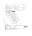
- the value B shown in FIG. 5 is the integrated exposure amount of the second exposure area 31 b of the exposure area 31.
- the integrated exposure amount r4 in the non-exposure region 32 (t2 to t4) is lower than the photoresist sensitivity threshold
- the integrated exposure amount r6 in the portion after t0 to t1 and t5 is the photoresist sensitivity threshold. Is over. Between t1 to t2 and t4 to t5, there are a portion below and above a photoresist sensitivity threshold.
- the integrated exposure amount of the entire region on both sides in the relative movement direction of the non-exposure region 32 is higher than that of the first embodiment after the exposure process. Specifically, a portion exceeding the photoresist sensitivity threshold in the first adjacent region 31A (t1 to t2) adjacent to the rear side of the non-exposed region 32 and the second adjacent region 31B adjacent to the front side of the non-exposed region 32 In (t4 to t5), the portion exceeding the photoresist sensitivity threshold increases. That is, the weakly exposed area below the photoresist sensitivity threshold is small. As described above, with this apparatus, sufficient exposure is performed on both sides of the non-exposure area in the relative movement direction. Therefore, the quality of the boundary in the scanning direction is improved. In this embodiment, the integrated exposure amount r5 in the first exposure region 31a and the third exposure region 31c of the exposure region 31 is constant.
- the non-exposure area is formed inside the exposure area by turning off the second row portion 13b of the exposure head 4, but the non-exposure area may be formed at the end of the exposure area in the Y direction. Good. Therefore, in the third embodiment described below, the non-exposure region is formed by turning off the first row portion 13a of the exposure head 4. Only the parts different from the first embodiment will be described below.
- FIG. 6 is a diagram showing the position and state of the light source with respect to the time axis, the exposure state of the exposure object, and the integrated exposure amount in the third embodiment. A value C shown in FIG.
- FIG. 6 is an integrated exposure amount of the first exposure area 31 a of the exposure area 31.
- a non-exposure region 33 is formed in the first exposure region 31 a within the exposure region 31.
- Control of turning on / off the exposure head 4 is the same as in the first embodiment. Further, as a result of the above series of operations, the obtained result is the same as that of the first embodiment.
- peripheral exposure apparatus (fourth embodiment)
- both sides of the non-exposure area 33 in the relative movement direction (t1 to t2 and t4 to t5) are not affected by the turn-off of the first row portion 13a of the exposure head 4 although they are not non-exposure areas. Is receiving. Therefore, depending on the conditions, it is conceivable that the integrated exposure amount approaches or falls below the photoresist sensitivity threshold. Therefore, in the fourth embodiment, a part of the third embodiment is changed in order to solve such a problem in advance.
- the second row portion 13b of the exposure head 4 has higher illuminance than the first row portion 13a and the third row portion 13c. More specifically, unlike the second embodiment, the illuminance of the light-emitting element for turning off during non-exposure is increased when the exposure head 4 moves to a predetermined area (on the non-exposure area) on both sides in the relative movement direction of the non-exposure area. Only when it is in an adjacent area. Thereby, the influence of exposure by increasing the illuminance of the non-exposure light-emitting element is limited to a certain region.
- FIG. 7 is a control flowchart of the exposure operation in the fourth embodiment.
- FIG. 8 is a diagram showing the position and state of the light source with respect to the time axis, the exposure state of the exposure object, and the integrated exposure amount in the fourth embodiment.
- a value D shown in FIG. 8 is an integrated exposure amount of the first exposure area 31 a of the exposure area 31.
- step S1 the exposure head 4 is turned on. At this time, all the light emitting diodes 13 emit light. In this case, the illuminance of all the light emitting diodes 13 is the same.
- step S2 the exposure head 4 is started to move relative to the substrate S (hereinafter referred to as a first exposure step).
- step S ⁇ b> 11 it is determined whether the exposure head 4 has reached the front side position ahead of the first position 26 with respect to the substrate S.
- the front side position is a position when the tip 4a of the exposure head 4 reaches t1.
- step S12 the first row portion 13a has higher illuminance than the first row portion 13a and the second row portion 13b (hereinafter, the third exposure step in the first exposure step).
- the illuminance of the first row portion 13a is, for example, about 1.5 times and preferably 1.2 to 1.8 times the illuminance of the second row portion 13b and the third row portion 13c.
- step S3 the exposure head 4 reaches the non-exposure position, specifically, the tip 4a end of the exposure head 4 reaches the non-exposure region start position (t2). Wait for position 1 to arrive.
- step S4 the second row portion 13b of the exposure head 4 is turned off (hereinafter referred to as a second exposure step).
- step S5 the exposure head 4 leaves the non-exposure area. Specifically, the rear end 4b of the exposure head 4 reaches the non-exposure area end position (t4), that is, the exposure head 4 is the fifth in FIG. Wait for position 30 to be reached.
- step S6 the first row portion 13a of the exposure head 4 is turned on. At this time, the first row portion 13a has higher illuminance than the second row portion 13b and the third row portion 13c (hereinafter, the third exposure step in the first exposure step).
- the illuminance of the first row portion 13a is, for example, about 1.5 times and preferably 1.2 to 1.8 times the illuminance of the second row portion 13b and the third row portion 13c.
- step S13 it is determined whether the exposure head 4 has reached the rear position on the rear side in the relative movement direction with respect to the substrate S from the fifth position 30.
- the rear end 4b of the exposure head 4 reaches t6.
- step S14 the illuminance of the first row portion 13a is lowered to the same level as the second row portion 13b and the third row portion 13c (hereinafter, the first exposure step).
- step S7 the process waits for the exposure head 4 to reach the end of the exposure area of the substrate S.
- step S8 the exposure head 4 is turned off.
- step S9 the XY stage 2 ends the operation.
- the integrated exposure amount of the entire region on both sides in the relative movement direction of the non-exposure region 33 is higher than that in the third embodiment. Therefore, in the first exposure region 31a of the exposure region 31, the first adjacent region 31A (t1 to t2) adjacent to the rear side of the non-exposure region 33 and the second adjacent region 31B (t4) adjacent to the front side of the non-exposure region 33.
- the cumulative exposure amount of .about.t5) increases, and the portion exceeding the photoresist sensitivity threshold increases. That is, the portion lower than the photoresist sensitivity threshold is smaller than that in the third embodiment.
- the region where the illuminance of the first row portion 13a of the exposure head 4 is increased is limited to a partial region adjacent to both sides of the non-exposure region 33.
- the integrated exposure amount of the third adjacent region 31C adjacent to the rear side of the first adjacent region 31A is larger than the integrated exposure amount of the first adjacent region 31A. It is not excessively higher than the rear side of the region 31C.
- the integrated exposure amount of the fourth adjacent area 31D adjacent to the front side of the second adjacent area 31B is larger than that of the second adjacent area 31B, but is excessively higher than the front side of the fourth adjacent area 31D. is not.
- the region where the integrated exposure amount is large is limited and the degree thereof is small, so that it is possible to prevent the end face from being disturbed by the influence of leakage light.
- the present invention can be widely applied to peripheral exposure apparatuses.
Landscapes
- Physics & Mathematics (AREA)
- General Physics & Mathematics (AREA)
- Exposure Of Semiconductors, Excluding Electron Or Ion Beam Exposure (AREA)
- Exposure And Positioning Against Photoresist Photosensitive Materials (AREA)
- Liquid Crystal (AREA)
- Led Device Packages (AREA)
Abstract
周辺露光装置(1)は、基板(S)の周辺を露光するための装置であって、露光ヘッド(4)と、XYステージ(2)と、制御装置(23)とを備えている。露光ヘッド(4)は、基板(S)と相対移動するX方向に直交するY方向に並んだ複数の発光ダイオード(13)を有する。XYステージ(2)は、露光ヘッド(4)と基板(S)を相対移動させる。制御装置(23)は、相対移動中に複数の発光ダイオード(13)の発光状態を制御するための制御部である。制御装置(23)は、基板(S)を露光するために複数の発光ダイオード(13)を点灯する。また、制御装置(23)は、露光動作中に露光領域(31)内に非露光領域(32)を確保するために複数の発光ダイオード(13)のうち非露光領域(32)に対応する非露光時消灯用の第2列部分(13b)を消灯する。
Description
本発明は、液晶用ガラス基板、半導体ウエハー、感光フィルムなどの露光対象物の周辺所定位置を露光するための周辺露光装置および周辺露光方法に関する。
従来から、液晶用ガラス基板、半導体ウエハー、感光フィルムなどの露光対象物の周辺所定位置を露光するための周辺露光装置が提供され、実用に供されている。
液晶表示パネル、または半導体ウエハー等の基板に配線パターンを形成する際は、先ず基板全面にレジストを塗布し、フォトリソグラフィ法により所望の形状にパターニングして配線パターンが製作される。その際に、通常は、基板周辺部に幅が数mm程度の帯状の余白が製作されるように、マスクパターンの露光位置が決められている。
このため、フォトリソグラフィ工程でポジ型レジストを使用すると、現像処理後、基板周辺部に未露光のレジストが帯状に残存することになる。未露光のレジストが残存すると、下の成膜がエッチング除去されない。そうすると、下の成膜の上に、次の成膜が積層されていくことになるため、後の工程で問題となる。そこで、基板周辺部の不要なレジスト領域を露光・現像して除去する必要がある。
このような問題点を考慮して、従来から、角形基板の周辺露光装置として、例えば、特許文献1に記載された装置が知られている。
従来の周辺露光装置では、露光対象物の周辺部分を連続的に露光するが、周辺露光領域内の一部の領域を非露光領域として残すことがある。これは、その前後に、非露光領域に識別コード等のパターンを形成するためである。識別コードは、プロセス毎および製造ライン全体の歩留まりを向上させるための履歴管理や品質管理等に利用されている。
従来の装置では、露光ヘッドと露光対象物を相対的に移動させることで、連続露光を実現していた。そして、特許文献1に記載の周辺露光装置では、非露光領域を残すためには、露光ヘッドから放射された紫外線の一部を遮蔽板によって遮光している。または、走査中に露光ヘッドの幅方向位置を変更することで非露光領域を形成する周辺露光装置も知られている。
遮蔽板を用いる方法では、遮蔽板を速度制御しながら駆動する必要があり、その結果、機構が複雑になっていた。また、露光ヘッドをいったん停止させて幅方向位置を変更することで非露光部分を残す方法では、処理時間が長くなっていた。つまり、生産性が低下していた。
本発明は上記の問題点に鑑みてなされたものであり、簡単な機構でかつ短い処理時間でもって、非露光部分を含む露光領域を形成可能な周辺露光装置および周辺露光方法を提供することを目的としている。
本発明の一見地に係る周辺露光装置は、露光対象物の周辺を露光するための周辺露光装置であって、光源と、移動装置と、制御部とを備えている。光源は、露光対象物と相対移動する方向に直交する幅方向に並んだ複数の発光素子を有する。移動装置は、光源と露光対象物を相対移動させる。制御部は、相対移動中に複数の発光素子の発光状態を制御する。制御部は、露光対象物を露光するために複数の発光素子を点灯する。また、制御部は、露光動作中に露光領域内に非露光領域を形成するために複数の発光素子のうち非露光領域に対応する非露光時消灯用発光素子を消灯する。
この装置では、露光動作中に非露光時消灯用発光素子が消灯されることで、露光領域内に非露光領域が形成される。したがって、光源と露光対象物の相対移動速度を遅くすることなく、露光領域と非露光領域を形成できる。このようにして、簡単な機構によって短時間で周辺露光が行われる。
この装置では、露光動作中に非露光時消灯用発光素子が消灯されることで、露光領域内に非露光領域が形成される。したがって、光源と露光対象物の相対移動速度を遅くすることなく、露光領域と非露光領域を形成できる。このようにして、簡単な機構によって短時間で周辺露光が行われる。
制御部は、光源が非露光領域に達すると非露光時消灯用発光素子を消灯して、光源が非露光領域から離れると非露光時消灯用発光素子を点灯してもよい。
この装置では、光源が非露光領域から離れると非露光時消灯用発光素子が点灯されるので、非露光領域以外領域では露光が行われる。
この装置では、光源が非露光領域から離れると非露光時消灯用発光素子が点灯されるので、非露光領域以外領域では露光が行われる。
制御部は、非露光領域以外を露光しているときに他の発光素子よりも非露光時消灯用発光素子の照度を高くしてもよい。
この装置では、非露光領域の相対移動方向両側においても、十分な露光が行われる。したがって、走査方向境目の品質が向上する。
この装置では、非露光領域の相対移動方向両側においても、十分な露光が行われる。したがって、走査方向境目の品質が向上する。
制御部は、非露光領域以外を露光しているときであって光源が非露光領域の相対移動方向両側に隣接する所定の領域にあるときのみ、他の発光素子よりも非露光時消灯用発光素子の照度を高くしてもよい。
この装置では、非露光時消灯用発光素子の照度が高くなるのは、光源が非露光領域の相対移動方向両側に隣接する所定の領域にあるときのみなので、非露光領域以外の部分において非露光時消灯用発光素子の照度を高くすることによる露光の影響を与える領域が限定されている。これは、特に、非露光領域が露光領域の幅方向端面に露出している場合に、つまり、非露光時消灯用発光素子が露光ヘッドの幅方向端部に配置されている場合に、顕著な効果が得られる。なぜなら、露光領域の幅方向端面に対応する非露光時消灯用発光素子の照度が高いと、露光領域の幅方向端面における露光が過度になり露光領域の端面が乱れるという不具合が生じることがあるからである。
この装置では、非露光時消灯用発光素子の照度が高くなるのは、光源が非露光領域の相対移動方向両側に隣接する所定の領域にあるときのみなので、非露光領域以外の部分において非露光時消灯用発光素子の照度を高くすることによる露光の影響を与える領域が限定されている。これは、特に、非露光領域が露光領域の幅方向端面に露出している場合に、つまり、非露光時消灯用発光素子が露光ヘッドの幅方向端部に配置されている場合に、顕著な効果が得られる。なぜなら、露光領域の幅方向端面に対応する非露光時消灯用発光素子の照度が高いと、露光領域の幅方向端面における露光が過度になり露光領域の端面が乱れるという不具合が生じることがあるからである。
制御部は、非露光領域以外を露光しているときに他の発光素子よりも非露光時消灯用発光素子の照度を1.2~1.8倍に高くしてもよい。
非露光時消灯用発光素子は、複数の発光素子の中で、露光対象物と相対移動する方向に直交する幅方向の中間部に配置されていてもよい。
非露光時消灯用発光素子は、複数の発光素子の中で、露光対象物と相対移動する方向に直交する幅方向の端部に配置されていてもよい。
本発明の他の見地に係る周辺露光方法は、露光対象物の周辺を露光するための方法である。この方法は、露光対象物と相対移動する方向に直交する幅方向に並んだ複数の発光素子を有する光源と、光源と露光対象物を相対移動させるための移動装置とを備えた周辺露光装置に使用される。周辺露光方法は、以下のステップを備えている。
◎露光対象物を露光するために複数の発光素子を全て点灯しながら露光動作を行う第1露光ステップ
◎露光領域内に非露光領域を形成するために複数の発光素子のうち非露光時消灯用発光素子を消灯した状態で露光動作を行う第2露光ステップ
この方法では、露光動作中に非露光時消灯用発光素子が消灯されることで、露光領域内に非露光領域が形成される。したがって、光源と露光対象物の相対移動速度を遅くすることなく、露光領域と非露光領域を形成できる。このようにして、簡単な機構によって短時間で周辺露光が行われる。
◎露光対象物を露光するために複数の発光素子を全て点灯しながら露光動作を行う第1露光ステップ
◎露光領域内に非露光領域を形成するために複数の発光素子のうち非露光時消灯用発光素子を消灯した状態で露光動作を行う第2露光ステップ
この方法では、露光動作中に非露光時消灯用発光素子が消灯されることで、露光領域内に非露光領域が形成される。したがって、光源と露光対象物の相対移動速度を遅くすることなく、露光領域と非露光領域を形成できる。このようにして、簡単な機構によって短時間で周辺露光が行われる。
第1露光ステップは、第2露光ステップの前後にそれぞれ実行されてもよい。
第1露光ステップは、非露光領域以外を露光しているときに他の発光素子よりも非露光時消灯用発光素子の照度を高くする第3露光ステップを含んでいてもよい。
この方法では、非露光領域の相対移動方向両側においても、十分な露光が行われる。したがって、走査方向境目の品質が向上する。
この方法では、非露光領域の相対移動方向両側においても、十分な露光が行われる。したがって、走査方向境目の品質が向上する。
第3露光ステップは、光源が非露光領域の相対移動方向両側に隣接する所定の領域にあるときのみ実行されてもよい。
この方法では、非露光時消灯用発光素子の照度が高くなるのは、光源が非露光領域の相対移動方向両側に隣接する所定の領域にあるときのみなので、非露光領域以外の部分において非露光時消灯用発光素子の照度を高くすることによる露光の影響を与える領域が限定されている。これは、特に、非露光領域が露光領域の幅方向端面に露出している場合に、つまり、非露光時消灯用発光素子が露光ヘッドの幅方向端部に配置されている場合に、顕著な効果が得られる。なぜなら、露光領域の幅方向端面に対応する非露光時消灯用発光素子の照度が高いと、露光領域の幅方向端面における露光が過度になり露光領域の端面が乱れるという不具合が生じることがあるからである。
この方法では、非露光時消灯用発光素子の照度が高くなるのは、光源が非露光領域の相対移動方向両側に隣接する所定の領域にあるときのみなので、非露光領域以外の部分において非露光時消灯用発光素子の照度を高くすることによる露光の影響を与える領域が限定されている。これは、特に、非露光領域が露光領域の幅方向端面に露出している場合に、つまり、非露光時消灯用発光素子が露光ヘッドの幅方向端部に配置されている場合に、顕著な効果が得られる。なぜなら、露光領域の幅方向端面に対応する非露光時消灯用発光素子の照度が高いと、露光領域の幅方向端面における露光が過度になり露光領域の端面が乱れるという不具合が生じることがあるからである。
非露光領域以外を露光しているときに他の発光素子よりも非露光時消灯用発光素子の照度は1.2~1.8倍であってもよい。
本発明のさらに他の見地に係る記録媒体は、上記の周辺露光方法をコンピュータに実行させるためのプログラムが格納されている。
本発明に係る周辺露光装置および周辺露光方法では、簡単な機構でかつ短い処理時間でもって、非露光部分を含む露光領域を形成できる。
(1)本実施形態の概要
周辺露光装置は、露光対象物の周辺を露光するための装置(例えば、周辺露光装置1)であって、光源(例えば、露光ヘッド4)と、移動装置(例えば、XYステージ2)と、制御部(例えば、制御装置23)とを備えている。光源は、露光対象物(例えば、基板S)と相対移動する方向(例えば、X方向)に直交する幅方向(例えば、Y方向)に並んだ複数の発光素子(例えば、発光ダイオード13)を有する。移動装置は、光源と露光対象物を相対移動させる。制御部は、相対移動中に複数の発光素子の発光状態を制御する。制御部は、露光対象物を露光するために複数の発光素子を点灯するとともに、露光動作中に露光領域内に非露光領域を形成するために複数の発光素子のうち非露光領域に対応する非露光時消灯用発光素子(例えば、第2列部分13b)を消灯する。
この装置では、露光動作中に非露光時消灯用発光素子が消灯されることで、露光領域内に非露光領域(例えば、非露光領域32)が形成される。したがって、光源と露光対象物の相対移動速度を遅くすることなく、露光領域と非露光領域を形成できる。このようにして、簡単な機構によって短時間で周辺露光が行われる。
周辺露光装置は、露光対象物の周辺を露光するための装置(例えば、周辺露光装置1)であって、光源(例えば、露光ヘッド4)と、移動装置(例えば、XYステージ2)と、制御部(例えば、制御装置23)とを備えている。光源は、露光対象物(例えば、基板S)と相対移動する方向(例えば、X方向)に直交する幅方向(例えば、Y方向)に並んだ複数の発光素子(例えば、発光ダイオード13)を有する。移動装置は、光源と露光対象物を相対移動させる。制御部は、相対移動中に複数の発光素子の発光状態を制御する。制御部は、露光対象物を露光するために複数の発光素子を点灯するとともに、露光動作中に露光領域内に非露光領域を形成するために複数の発光素子のうち非露光領域に対応する非露光時消灯用発光素子(例えば、第2列部分13b)を消灯する。
この装置では、露光動作中に非露光時消灯用発光素子が消灯されることで、露光領域内に非露光領域(例えば、非露光領域32)が形成される。したがって、光源と露光対象物の相対移動速度を遅くすることなく、露光領域と非露光領域を形成できる。このようにして、簡単な機構によって短時間で周辺露光が行われる。
(2)周辺露光装置の構造
図1を用いて、周辺露光装置1について説明する。図1は、周辺露光装置の一実施形態を概略的に示す斜視図である。
図1を用いて、周辺露光装置1について説明する。図1は、周辺露光装置の一実施形態を概略的に示す斜視図である。
周辺露光装置1は、例えば、液晶パネルの周辺露光に適用される。
周辺露光装置1は、レジストが塗布された基板Sを支承するXYステージ2と、XYステージ2を支承する回転テーブル3とを有している。周辺露光装置1は、さらに、基板Sに対する周辺露光を行う露光ヘッド4と、露光ヘッド4を保持するスライダー5とを有している。周辺露光装置1は、さらに、露光ヘッド4の出力光強度を検出する照度計6と、露光ヘッド4に駆動電流を供給する直流電源7と、露光ヘッド4の温度を制御する温度制御機構8とを有している。
基板Sとしては、ガラス基板、他の材質製の基板、半導体ウエハー、フィルムなどが例示できる。また、種々の形状のものが採用可能である。
XYステージ2は、基板Sを2次元的に移動させるものである。この実施形態では、XYステージ2は基板SをX方向に移動できる。回転テーブル3は、XYステージ2と共に基板Sを回転させるものである。
図2を用いて、露光ヘッド4を説明する。図2は、発光ダイオードを碁盤目状5行5列に配列した周辺露光用光源を示す概略図および側面図である。露光ヘッド4は、矩形状の基体11と、複数の発光ダイオード13と、複数の光学系部材15とから構成されている。
基体11は、複数の発光ダイオード13を保持する部材であり、概ね正方形の板状部材である。複数の発光ダイオード13は、基体11の下面に設けられ、下方に紫外線を放射することが可能である。
複数の発光ダイオード13は、縦横に整列した状態で配置されている。図2では、発光ダイオード13は、5×5で並べられているが、実際は例えば17mm角に17×17で並べられている。
光学系部材15は、発光ダイオード13に対応して下方に配置されている。発光ダイオード13から発射された紫外線は、光学系部材15を通過することで広がりを防止されている。これにより、露光エリアの寸法精度を高めることができる。
基体11は、複数の発光ダイオード13を保持する部材であり、概ね正方形の板状部材である。複数の発光ダイオード13は、基体11の下面に設けられ、下方に紫外線を放射することが可能である。
複数の発光ダイオード13は、縦横に整列した状態で配置されている。図2では、発光ダイオード13は、5×5で並べられているが、実際は例えば17mm角に17×17で並べられている。
光学系部材15は、発光ダイオード13に対応して下方に配置されている。発光ダイオード13から発射された紫外線は、光学系部材15を通過することで広がりを防止されている。これにより、露光エリアの寸法精度を高めることができる。
スライダー5は、露光ヘッド4をY方向(X方向に直交している)に往復動させるものである。
照度計6は、スライダー5による露光ヘッド4の移動限界位置において露光ヘッド4の出力光を受光するものであり、強度検出信号を直流電源7に供給する。
直流電源7は、所定の出力光強度が得られるように、露光ヘッド4に駆動電圧または電流を供給する電源本体21と、制御装置23とを有している。
制御装置23は、入力機能、記憶機能、比較演算機能、動作指令機能等を備えたコンピュータまたはプログラマブルロジックアレイである。制御装置23は、発光ダイオード13を露光時のみ発光させ、また、必要に応じて露光条件を変化させるように、駆動電圧または電流を制御する。制御装置23は、上記制御を行うために、あらかじめ品種別の駆動電圧または電流のデータを保存している。制御装置23は、図に示すように、CPU23a,メモリ23bを有している。メモリ23bは、制御プログラムが格納されている記録媒体である。
制御装置23には、XYステージ2およびスライダー5から、基板Sに対する露光ヘッド4の位置を知らせるために位置信号が入力される。
制御装置23は、入力機能、記憶機能、比較演算機能、動作指令機能等を備えたコンピュータまたはプログラマブルロジックアレイである。制御装置23は、発光ダイオード13を露光時のみ発光させ、また、必要に応じて露光条件を変化させるように、駆動電圧または電流を制御する。制御装置23は、上記制御を行うために、あらかじめ品種別の駆動電圧または電流のデータを保存している。制御装置23は、図に示すように、CPU23a,メモリ23bを有している。メモリ23bは、制御プログラムが格納されている記録媒体である。
制御装置23には、XYステージ2およびスライダー5から、基板Sに対する露光ヘッド4の位置を知らせるために位置信号が入力される。
また、照度計6により、定期的に出力光強度を測定し、出力光強度測定値を制御装置23に供給し、適切な発光ダイオード13の照射状態を演算させることが好ましく、発光ダイオードが経時劣化した場合でも安定した露光品質を実現できる。
温度制御機構8は、冷却水を生成するためのチラー8aと、冷却水を露光ヘッド4のブラケット(図示せず)に供給して発光ダイオード13を冷却し、再びチラー8aに戻すための冷却水流路8bを有している。温度制御機構8は、さらに、冷却水流路8bに沿って、冷却水流路8bの所定位置に設けたバルブ8c、流量計8d、水圧計8e、および水温センサー8fを有している。なお、水温センサー8fは、ブラケット(図示せず)のすぐ下流側に設けられており、温度検出信号をチラー8aに供給して、チラー8aの動作を制御する。
また、基板Sの搬入、搬出は、図示しない基板移搭ロボット、シャトル搬送移載機構、ローラコンベア等によって行うか、作業者の手作業によって行う。
さらに、図示しないL字状位置合わせガイドもしくはL字状の3点のみ接触するピン型のガイドを設けることが好ましく、XYステージ2に供給された基板Sの位置がずれている場合に、該ガイドに基板Sを押し付けて位置を合わせることができる。
(3)周辺露光装置の動作(概略説明)
周辺露光装置1の動作を概略的に説明する。なお、以下、図示しない識別露光装置によって、基板Sに識別コードはあらかじめ形成されているとして説明する。
周辺露光装置1の動作を概略的に説明する。なお、以下、図示しない識別露光装置によって、基板Sに識別コードはあらかじめ形成されているとして説明する。
最初に、レジストが塗布された基板Sが周辺露光装置1に搬入される。次に、XYステージ2、回転テーブル3が駆動されて基板Sの位置決めが行われる。次に、スライダー5によって、露光ヘッド4を露光すべき周辺位置に正対させる。以上により、周辺露光の準備が完了する。
続いて、XYステージ2によって基板SをX方向に移動させるとともに、直流電源7により露光ヘッド4を動作させることによって、基板Sの1辺に沿って周辺部の不要レジストを露光する。
次いで、XYステージ2、回転テーブル3を動作させるとともに、スライダー5を動作させることによって、露光ヘッド4を他の辺の露光すべき周辺位置に正対させる。そして、基板Sの該当する辺に沿って、周辺部の不要レジストを露光する。
同様にして、基板Sの全ての辺に沿って周辺部の不要レジストを露光する。
同様にして、基板Sの全ての辺に沿って周辺部の不要レジストを露光する。
以上の処理を行えば、矩形の基板Sの4辺全ての周辺露光をことができるが、露光するのはいずれかの辺のみであってもよい。また、周辺部の露光以外に基板内部への露光を行うことも可能である。なお、他の装置に本機能を組み込まれた場合等は、いずれの辺も露光しない場合もある。
あらかじめ露光したい形状全面、またはその形状を分割した形状に露光ヘッド4を配し、ステージを静止した状態で、必要時間照射し露光することも可能である。
また、不要レジスト部への露光の最中にXYステージ2と回転テーブル3とスライダー5とを動作させ、露光端面に凹凸のある形状に合わせて周辺露光を行うことも可能である。
(4)周辺露光装置の動作(第1実施形態)
図3および図4を用いて、第1実施形態における周辺露光装置1の動作を詳細に説明する。図3は、第1実施形態における露光動作の制御フローチャートである。図4は、第1実施形態における時間軸に対する光源の位置および状態、露光対象物の露光状態、積算露光量を示した図である。
以下、図4において、図左右方向がX方向であり、露光ヘッド4は基板Sに対して図右側に移動する動作を説明する。そこで、図右側を「先側」として、図左側を「後側」と称する。図4において、X方向に対して直交する方向をY方向とする。
図3および図4を用いて、第1実施形態における周辺露光装置1の動作を詳細に説明する。図3は、第1実施形態における露光動作の制御フローチャートである。図4は、第1実施形態における時間軸に対する光源の位置および状態、露光対象物の露光状態、積算露光量を示した図である。
以下、図4において、図左右方向がX方向であり、露光ヘッド4は基板Sに対して図右側に移動する動作を説明する。そこで、図右側を「先側」として、図左側を「後側」と称する。図4において、X方向に対して直交する方向をY方向とする。
図4に示すように、露光ヘッド4の発光ダイオード13は、Y方向に、第1列部分13a、第2列部分13b、第3列部分13cに分かれている。各部分は、発光ダイオード13の単数または複数の列から構成されている。
露光領域31は、Y方向に所定の幅を有しながらX方向に長く延びる領域である。つまり、露光領域31の長手方向がX方向であり、短手方向または幅方向がY方向である。露光ヘッド4の第1列部分13aに対応する第1露光領域31a、露光ヘッド4の第2列部分13bに対応する第2露光領域31b、露光ヘッド4の第3列部分13cに対応する第3露光領域31cに分かれている。第2露光領域31bにおいて、識別コードが先にマークされている部分を非露光領域32とする。
図4において、グラフの横軸は時間であるが、露光ヘッド4と基板Sの相対速度は一定であるので、移動距離であると考えてもよい。図4において、t0が相対移動開始点であり、t1、t2、t3、t4、t5、t6の各間は等間隔である。また、t1~t6では、時刻間2つ分が露光ヘッド4の相対方向長さに対応している。図4では、露光ヘッド4が、基板Sに対して、第1位置26、第2位置27、第3位置28、第4位置29、第5位置30にある状態を示している。第1位置26では、露光ヘッド4の先端4aがt2に対応している。第2位置27では、露光ヘッド4の先端4aがt3に対応しており、露光ヘッド4の後端4bがt1に対応している。第3位置28では、露光ヘッド4の先端4aがt4に対応しており、露光ヘッド4の後端4bがt2に対応している。第4位置29では、露光ヘッド4の先端4aがt5に対応しており、露光ヘッド4の後端4bがt3に対応している。第5位置30では、露光ヘッド4の先端4aがt6に対応しており、露光ヘッド4の後端4bがt4に対応している。
図3において、周辺露光装置1が一直線状に周辺露光を行う動作を説明する。
ステップS1では、直流電源7が露光ヘッド4を点灯する。このときに、全ての発光ダイオード13が点灯される。具体的には、制御装置23が電源本体21に駆動信号を送信して、電源本体21から露光ヘッド4に例えば電圧が印加される。
ステップS1では、直流電源7が露光ヘッド4を点灯する。このときに、全ての発光ダイオード13が点灯される。具体的には、制御装置23が電源本体21に駆動信号を送信して、電源本体21から露光ヘッド4に例えば電圧が印加される。
ステップS2では、XYステージ2が基板Sを露光ヘッド4に対してX方向に移動させる動作を開始する。以後、基板Sは露光ヘッド4に対して一定速度で相対移動を続ける(第1露光ステップ)。なお、図4では、露光ヘッド4が基板Sに対してX方向先側(図右側)に移動するとして説明する。
ステップS3では、露光ヘッド4が非露光位置に到達するのを、具体的には露光ヘッド4の先端4a端が非露光領域開始位置(t2)に達する、つまり、露光ヘッド4が図4の第1位置26に到達するのを待つ。
ステップS4では、露光ヘッド4の第2列部分13bが消灯される(以後、第2露光ステップ)。
ステップS5では、露光ヘッド4が非露光領域から離脱するのを、具体的には露光ヘッド4の後端4bが非露光領域終了位置(t4)に達する、つまり露光ヘッド4が図4の第5位置30に到達するのを待つ。
ステップS6では、露光ヘッド4の第2列部分13bが点灯される。つまり、光源が非露光領域から離れると非露光時消灯用発光素子は点灯されるので、非露光領域以外領域では非露光時消灯用発光素子による露光が行われる。これ以降は、露光ヘッド4では全ての発光ダイオード13が点灯している状態である(第1露光ステップ)。
ステップS7では、露光ヘッド4が基板Sの露光領域の終端に達するのを待つ。
ステップS8では、露光ヘッド4が消灯される。
ステップS9では、XYステージ2が動作を終了する。
ステップS5では、露光ヘッド4が非露光領域から離脱するのを、具体的には露光ヘッド4の後端4bが非露光領域終了位置(t4)に達する、つまり露光ヘッド4が図4の第5位置30に到達するのを待つ。
ステップS6では、露光ヘッド4の第2列部分13bが点灯される。つまり、光源が非露光領域から離れると非露光時消灯用発光素子は点灯されるので、非露光領域以外領域では非露光時消灯用発光素子による露光が行われる。これ以降は、露光ヘッド4では全ての発光ダイオード13が点灯している状態である(第1露光ステップ)。
ステップS7では、露光ヘッド4が基板Sの露光領域の終端に達するのを待つ。
ステップS8では、露光ヘッド4が消灯される。
ステップS9では、XYステージ2が動作を終了する。
上記の一連動作の結果、露光動作中に非露光時消灯用発光素子が消灯されるので、露光領域31内に非露光領域32が確保される。したがって、露光ヘッド4と基板Sの相対移動速度を遅くすることなく、露光領域と非露光領域を形成できる。このようにして、簡単な機構によって短時間で周辺露光が行われる。
ここで、図4のグラフに基づいて露光領域および非露光領域の積算露光量を説明する。図4に示された値Aは、露光領域31の第2露光領域31bの積算露光量である。図から明らかなように、非露光領域32(t2~t4)において積算露光量r1はフォトレジスト感度閾値を下回っており、t0~t1およびt5以降の部分の積算露光量は、フォトレジスト感度領域を上回っている。t1~t2、t4~5との間は、フォトレジスト感度閾値を下回る部分と上回る部分とがある。
なお、露光領域31の第1露光領域31aおよび第3露光領域31cにおける積算露光量は、一定であり、第2露光領域31bのt0~t1およびt5以降の値r3と同じである。
ここで、図4のグラフに基づいて露光領域および非露光領域の積算露光量を説明する。図4に示された値Aは、露光領域31の第2露光領域31bの積算露光量である。図から明らかなように、非露光領域32(t2~t4)において積算露光量r1はフォトレジスト感度閾値を下回っており、t0~t1およびt5以降の部分の積算露光量は、フォトレジスト感度領域を上回っている。t1~t2、t4~5との間は、フォトレジスト感度閾値を下回る部分と上回る部分とがある。
なお、露光領域31の第1露光領域31aおよび第3露光領域31cにおける積算露光量は、一定であり、第2露光領域31bのt0~t1およびt5以降の値r3と同じである。
(5)周辺露光装置の動作(第2実施形態)
前記実施形態では、非露光領域32の両側(t1~t2およびt4~t5)は、非露光領域でないにもかかわらず、露光ヘッド4の第2列部分13bの消灯の影響を受けて積算露光量がフォトレジスト感度閾値に近くなるまたは下回ることが考えられる。そこで、第2実施形態ではそのような問題をあらかじめ解決するために第1実施形態の一部を変更している。以下、第1実施形態と異なる部分を中心に説明する。
前記実施形態では、非露光領域32の両側(t1~t2およびt4~t5)は、非露光領域でないにもかかわらず、露光ヘッド4の第2列部分13bの消灯の影響を受けて積算露光量がフォトレジスト感度閾値に近くなるまたは下回ることが考えられる。そこで、第2実施形態ではそのような問題をあらかじめ解決するために第1実施形態の一部を変更している。以下、第1実施形態と異なる部分を中心に説明する。
図3(第1実施形態と共通)及び図5を用いて、第2実施形態を説明する。図2は、発光ダイオードを碁盤目状5行5列に配列した周辺露光用光源を示す概略図および側面図である。
ステップS1では、露光ヘッド4を点灯する。このとき、全ての発光ダイオード13が発光するが、第2列部分13bは、第1列部分13aおよび第2列部分13bに比べて照度が高められる。第1列部分13aおよび第2列部分13bの照度に対して、第2列部分13bの照度は、例えば約1.5倍であり、1.2~1.8倍であることが好ましい。
ステップS1では、露光ヘッド4を点灯する。このとき、全ての発光ダイオード13が発光するが、第2列部分13bは、第1列部分13aおよび第2列部分13bに比べて照度が高められる。第1列部分13aおよび第2列部分13bの照度に対して、第2列部分13bの照度は、例えば約1.5倍であり、1.2~1.8倍であることが好ましい。
ステップS2では、XYステージ2が基板Sを露光ヘッド4に対してX方向に移動させる動作を開始する。以後、基板Sは露光ヘッド4に対して一定速度で相対移動を続ける(第1露光ステップ内の第3露光ステップ)。なお、図4では、露光ヘッド4が基板Sに対してX方向先側(図右側)に移動するとして説明する。
ステップS3では、露光ヘッド4が非露光位置に到達するのを、具体的には露光ヘッド4の先端4a端が非露光領域開始位置(t2)に達する、つまり、露光ヘッド4が図4の第1位置26に到達するのを待つ。
ステップS4では、露光ヘッド4の第2列部分13bが消灯される(以後、第2露光ステップ)。
ステップS5では、露光ヘッド4が非露光領域から離脱するのを、具体的には露光ヘッド4の後端4bが非露光領域終了位置(t4)に達する、つまり露光ヘッド4が図4の第5位置30に到達するのを待つ。
ステップS5では、露光ヘッド4が非露光領域から離脱するのを、具体的には露光ヘッド4の後端4bが非露光領域終了位置(t4)に達する、つまり露光ヘッド4が図4の第5位置30に到達するのを待つ。
ステップS6では、露光ヘッド4の第2列部分13bが点灯される。このとき、第2列部分13bは第1列部分13aおよび第3列部分13cに比べて照度が高められる(以後、第1露光ステップ内の第3露光ステップ)。第1列部分13aおよび第3列部分13cの照度に対して、第2列部分13bの照度は、例えば約1.5倍であり、1.2~1.8倍であることが好ましい。
ステップS7では、露光ヘッド4が基板Sの露光領域の終端に達するのを待つ。
ステップS8では、露光ヘッド4が消灯される。
ステップS9では、XYステージ2が動作を終了する。
ステップS7では、露光ヘッド4が基板Sの露光領域の終端に達するのを待つ。
ステップS8では、露光ヘッド4が消灯される。
ステップS9では、XYステージ2が動作を終了する。
上記の一連動作の結果、露光領域31内に非露光領域32が形成される。ここで、図5のグラフに基づいて露光領域および非露光領域の積算露光量を説明する。図5に示された値Bは、露光領域31の第2露光領域31bの積算露光量である。図から明らかなように、非露光領域32(t2~t4)の積算露光量r4はフォトレジスト感度閾値を下回っており、t0~t1およびt5以降の部分の積算露光量r6は、フォトレジスト感度閾値を上回っている。t1~t2、t4~t5との間は、フォトレジスト感度閾値を下回る部分と上回る部分とがある。
第1実施形態と異なる点として、露光処理後に、非露光領域32の相対移動方向両側の領域全体の積算露光量が第1実施形態より高くなっている。具体的には、非露光領域32の後側に隣接する第1隣接領域31A(t1~t2)においてフォトレジスト感度閾値を上回る部分、および非露光領域32の先側に隣接する第2隣接領域31B(t4~t5)においてフォトレジスト感度閾値を上回る部分が増える。つまり、フォトレジスト感度閾値を下回る弱露光領域が小さくなっている。以上に述べたように、この装置では、非露光領域の相対移動方向両側においても、十分な露光が行われる。したがって、走査方向境目の品質が向上する。
なお、この実施形態では、露光領域31の第1露光領域31aおよび第3露光領域31cにおける積算露光量r5は、一定である。
なお、この実施形態では、露光領域31の第1露光領域31aおよび第3露光領域31cにおける積算露光量r5は、一定である。
(6)周辺露光装置の動作(第3実施形態)
前記実施形態では、露光ヘッド4の第2列部分13bを消灯することによって非露光領域を露光領域の内部に形成していたが、非露光領域は露光領域のY方向端部に形成されてもよい。そこで、以下に述べる第3実施形態では、露光ヘッド4の第1列部分13aを消灯することで、非露光領域を形成する。以下、第1実施形態と異なる部分のみを説明する。
図6を用いて、第3実施形態を説明する。図6は、第3実施形態における時間軸に対する光源の位置および状態、露光対象物の露光状態、積算露光量を示した図である。図6に示された値Cは、露光領域31の第1露光領域31aの積算露光量である。
図6において、露光ヘッド4の第1列部分13aが消灯することで、露光領域31内で第1露光領域31aに非露光領域33が形成される。露光ヘッド4の点灯・消灯制御は第1実施形態と同様である。また、上記の一連動作の結果、得られた結果は第1実施形態と同じである。
前記実施形態では、露光ヘッド4の第2列部分13bを消灯することによって非露光領域を露光領域の内部に形成していたが、非露光領域は露光領域のY方向端部に形成されてもよい。そこで、以下に述べる第3実施形態では、露光ヘッド4の第1列部分13aを消灯することで、非露光領域を形成する。以下、第1実施形態と異なる部分のみを説明する。
図6を用いて、第3実施形態を説明する。図6は、第3実施形態における時間軸に対する光源の位置および状態、露光対象物の露光状態、積算露光量を示した図である。図6に示された値Cは、露光領域31の第1露光領域31aの積算露光量である。
図6において、露光ヘッド4の第1列部分13aが消灯することで、露光領域31内で第1露光領域31aに非露光領域33が形成される。露光ヘッド4の点灯・消灯制御は第1実施形態と同様である。また、上記の一連動作の結果、得られた結果は第1実施形態と同じである。
(7)周辺露光装置の動作(第4実施形態)
前述の第3実施形態では、非露光領域33の相対移動方向両側(t1~t2およびt4~t5)は、非露光領域でないにもかかわらず、露光ヘッド4の第1列部分13aの消灯の影響を受けている。したがって、条件によっては、積算露光量がフォトレジスト感度閾値に近くなり、又は下回ることが考えられる。そこで、第4実施形態ではそのような問題をあらかじめ解決するために第3実施形態の一部を変更している。
具体的には、非露光領域の両側では、第2実施形態のように、露光ヘッド4の第2列部分13bは第1列部分13aおよび第3列部分13cに比べて照度が高められる。さらに具体的には、第2実施形態とは異なり、非露光時消灯用発光素子の照度が高くされるのは、露光ヘッド4が非露光領域の相対移動方向両側の所定の領域(非露光領域に隣接する領域)にあるときのみとしている。それにより、非露光時消灯用発光素子の照度を高くすることによる露光の影響を、一定の領域を限定している。これは、特に、非露光領域が露光領域のY方向端面に露出している場合に、つまり、非露光時消灯用発光素子が露光ヘッドのY方向端部に配置されている場合に、顕著な効果が得られる。なぜなら、露光領域のY方向端面に対応する非露光時消灯用発光素子の照度が高いと、露光領域のY方向端面における露光が過度になり、漏れ光の影響により端面が乱れるといった不具合が生じることがあるからである。
前述の第3実施形態では、非露光領域33の相対移動方向両側(t1~t2およびt4~t5)は、非露光領域でないにもかかわらず、露光ヘッド4の第1列部分13aの消灯の影響を受けている。したがって、条件によっては、積算露光量がフォトレジスト感度閾値に近くなり、又は下回ることが考えられる。そこで、第4実施形態ではそのような問題をあらかじめ解決するために第3実施形態の一部を変更している。
具体的には、非露光領域の両側では、第2実施形態のように、露光ヘッド4の第2列部分13bは第1列部分13aおよび第3列部分13cに比べて照度が高められる。さらに具体的には、第2実施形態とは異なり、非露光時消灯用発光素子の照度が高くされるのは、露光ヘッド4が非露光領域の相対移動方向両側の所定の領域(非露光領域に隣接する領域)にあるときのみとしている。それにより、非露光時消灯用発光素子の照度を高くすることによる露光の影響を、一定の領域を限定している。これは、特に、非露光領域が露光領域のY方向端面に露出している場合に、つまり、非露光時消灯用発光素子が露光ヘッドのY方向端部に配置されている場合に、顕著な効果が得られる。なぜなら、露光領域のY方向端面に対応する非露光時消灯用発光素子の照度が高いと、露光領域のY方向端面における露光が過度になり、漏れ光の影響により端面が乱れるといった不具合が生じることがあるからである。
以下、第3実施形態と異なる部分を中心に説明する。
図7および図8を用いて、第4実施形態を説明する。図7は、第4実施形態における露光動作の制御フローチャートである。図8は、第4実施形態における時間軸に対する光源の位置および状態、露光対象物の露光状態、積算露光量を示した図である。図8に示された値Dは、露光領域31の第1露光領域31aの積算露光量である。
図7および図8を用いて、第4実施形態を説明する。図7は、第4実施形態における露光動作の制御フローチャートである。図8は、第4実施形態における時間軸に対する光源の位置および状態、露光対象物の露光状態、積算露光量を示した図である。図8に示された値Dは、露光領域31の第1露光領域31aの積算露光量である。
ステップS1では、露光ヘッド4が点灯される。このとき、全ての発光ダイオード13が発光する。この場合、全ての発光ダイオード13の照度は同じである。
ステップS2では、基板Sに対して露光ヘッド4が相対移動を開始させられる(以後、第1露光ステップ)。
ステップS11では、露光ヘッド4が基板Sに対して第1位置26より先側の先側位置に到達したかを判断される。先側位置とは、露光ヘッド4の先端4aがt1に到達したときの位置である。
ステップS12では、第1列部分13aは、第1列部分13aおよび第2列部分13bに比べて照度を高められる(以後、第1露光ステップ内の第3露光ステップ)。第2列部分13bおよび第3列部分13cの照度に対して、第1列部分13aの照度は、例えば約1.5倍であり、1.2~1.8倍であることが好ましい。
ステップS2では、基板Sに対して露光ヘッド4が相対移動を開始させられる(以後、第1露光ステップ)。
ステップS11では、露光ヘッド4が基板Sに対して第1位置26より先側の先側位置に到達したかを判断される。先側位置とは、露光ヘッド4の先端4aがt1に到達したときの位置である。
ステップS12では、第1列部分13aは、第1列部分13aおよび第2列部分13bに比べて照度を高められる(以後、第1露光ステップ内の第3露光ステップ)。第2列部分13bおよび第3列部分13cの照度に対して、第1列部分13aの照度は、例えば約1.5倍であり、1.2~1.8倍であることが好ましい。
ステップS3では、露光ヘッド4が非露光位置に到達するのを、具体的には露光ヘッド4の先端4a端が非露光領域開始位置(t2)に達する、つまり、露光ヘッド4が図4の第1位置26に到達するのを待つ。
ステップS4では、露光ヘッド4の第2列部分13bが消灯される(以後、第2露光ステップ)。
ステップS5では、露光ヘッド4が非露光領域から離脱するのを、具体的には露光ヘッド4の後端4bが非露光領域終了位置(t4)に達する、つまり露光ヘッド4が図4の第5位置30に到達するのを待つ。
ステップS5では、露光ヘッド4が非露光領域から離脱するのを、具体的には露光ヘッド4の後端4bが非露光領域終了位置(t4)に達する、つまり露光ヘッド4が図4の第5位置30に到達するのを待つ。
ステップS6では、露光ヘッド4の第1列部分13aが点灯される。このとき、第1列部分13aは、第2列部分13bおよび第3列部分13cに比べて照度を高められる(以後、第1露光ステップ内の第3露光ステップ)。第2列部分13bおよび第3列部分13cの照度に対して、第1列部分13aの照度は、例えば約1.5倍であり、1.2~1.8倍であることが好ましい。
ステップS13では、露光ヘッド4が基板Sに対して第5位置30より相対移動方向後側の後側位置に到達したかを判断する。露光ヘッド4が後側位置に到達するとは、露光ヘッド4の後端4bがt6に到達することをいう。
ステップS14では、第1列部分13aは、第2列部分13bおよび第3列部分13cと同じまで照度を低くさせられる(以後、第1露光ステップ)。
ステップS7では、露光ヘッド4が基板Sの露光領域の終端に達するのを待つ。
ステップS8では、露光ヘッド4が消灯される。
ステップS9では、XYステージ2が動作を終了する。
ステップS14では、第1列部分13aは、第2列部分13bおよび第3列部分13cと同じまで照度を低くさせられる(以後、第1露光ステップ)。
ステップS7では、露光ヘッド4が基板Sの露光領域の終端に達するのを待つ。
ステップS8では、露光ヘッド4が消灯される。
ステップS9では、XYステージ2が動作を終了する。
以上の結果、非露光領域33の相対移動方向両側の領域全体の積算露光量が、第3実施形態より高くなる。したがって、露光領域31の第1露光領域31aにおいて非露光領域33の後側に隣接する第1隣接領域31A(t1~t2)および非露光領域33の先側に隣接する第2隣接領域31B(t4~t5)の積算露光量が多くなり、フォトレジスト感度閾値を上回る部分が増える。つまり、フォトレジスト感度閾値よりも低くなる部分は、第3実施形態と比べて小さくなる。
さらに、この実施形態では、露光ヘッド4の第1列部分13aの照度を高くする領域は、非露光領域33の両側に隣接する部分的な領域に限定しているので、照度アップによる露光領域への悪影響を少なくできる。図8から明らかなように、第1隣接領域31Aの後側に隣接する第3隣接領域31Cの積算露光量は、第1隣接領域31Aの積算露光量よりも大きくなっているが、第3隣接領域31Cより後側と比べて過度に高くなっていない。また、第2隣接領域31Bの先側に隣接する第4隣接領域31Dの積算露光量は第2隣接領域31Bよりも大きくなっているが、第4隣接領域31Dより先側と比べて過度に高くなっていない。このように、積算露光量が大きい領域は限定されており、その程度も小さいため、漏れ光の影響による端面の乱れを防ぐことができる。
(8)他の実施形態
以上、複数の実施形態について説明したが、本発明は上記実施形態に限定されるものではなく、発明の要旨を逸脱しない範囲で種々の変更が可能である。
前記複数の実施形態は必要に応じて組み合わせることも可能である。例えば、露光領域の内部に非露光領域を形成する場合に、第4実施形態(図7、図8)のような点灯制御を行ってもよい。また、露光領域の端面に接する位置に非露光領域を形成する場合に、第2実施形態(図5)のような点灯制御を行ってもよい。
前記実施形態では光源と基板の相対速度は一定であるとしたが、必要に応じて変更してもよい。
前記実施形態では周辺露光動作の前に識別コードがマークさされていたが、識別露光動作の後に周辺露光動作を行ってもよい。
以上、複数の実施形態について説明したが、本発明は上記実施形態に限定されるものではなく、発明の要旨を逸脱しない範囲で種々の変更が可能である。
前記複数の実施形態は必要に応じて組み合わせることも可能である。例えば、露光領域の内部に非露光領域を形成する場合に、第4実施形態(図7、図8)のような点灯制御を行ってもよい。また、露光領域の端面に接する位置に非露光領域を形成する場合に、第2実施形態(図5)のような点灯制御を行ってもよい。
前記実施形態では光源と基板の相対速度は一定であるとしたが、必要に応じて変更してもよい。
前記実施形態では周辺露光動作の前に識別コードがマークさされていたが、識別露光動作の後に周辺露光動作を行ってもよい。
本発明は、周辺露光装置に広く適用できる。
1 周辺露光装置
2 XYテーブル
4 露光ヘッド(光源)
5 スライダー
6 照度計
7 直流電源
8 温度制御機構
8a チラー
8b 冷却水流路
8c バルブ
8d 流量計
8e 水圧計
8f センサー
11 基体
13 ダイオード
15 光学系部材
21 電源本体
23 制御装置
31 露光領域
32 非露光領域
33 非露光領域
2 XYテーブル
4 露光ヘッド(光源)
5 スライダー
6 照度計
7 直流電源
8 温度制御機構
8a チラー
8b 冷却水流路
8c バルブ
8d 流量計
8e 水圧計
8f センサー
11 基体
13 ダイオード
15 光学系部材
21 電源本体
23 制御装置
31 露光領域
32 非露光領域
33 非露光領域
Claims (13)
- 露光対象物の周辺を露光するための周辺露光装置であって、
前記露光対象物と相対移動する方向に直交する幅方向に並んだ複数の発光素子を有する光源と、
前記光源と前記露光対象物を相対移動させるための移動装置と、
相対移動中に前記複数の発光素子の発光状態を制御するための制御部であって、前記露光対象物を露光するために前記複数の発光素子を点灯し、露光動作中に露光領域内に非露光領域を形成するために前記複数の発光素子のうち前記非露光領域に対応する非露光時消灯用発光素子を消灯する制御部と、
を備えた周辺露光装置。 - 前記制御部は、前記光源が前記非露光領域に達すると前記非露光時消灯用発光素子を消灯して、前記光源が前記非露光領域から離れると前記非露光時消灯用発光素子を点灯する、請求項1に記載の周辺露光装置。
- 前記制御部は、前記非露光領域以外を露光しているときに他の発光素子よりも前記非露光時消灯用発光素子の照度を高くする、請求項2に記載の周辺露光装置。
- 前記制御部は、前記非露光領域以外を露光しているときであって前記光源が前記非露光領域の相対移動方向両側に隣接する所定の領域にあるときのみ、他の発光素子よりも前記非露光時消灯用発光素子の照度を高くする、請求項3に記載の周辺露光装置。
- 前記制御部は、前記非露光領域以外を露光しているときに他の発光素子よりも前記非露光時消灯用発光素子の照度を1.2~1.8倍に高くする、請求項3又は4に記載の周辺露光装置。
- 前記非露光時消灯用発光素子は、前記複数の発光素子の中で、前記露光対象物と相対移動する方向に直交する幅方向の中間部に配置されている、請求項1~5のいずれかに記載の周辺露光装置。
- 前記非露光時消灯用発光素子は、前記複数の発光素子の中で、前記露光対象物と相対移動する方向に直交する幅方向の端部に配置されている、請求項1~5のいずれかに記載の周辺露光装置。
- 露光対象物の周辺を露光するための周辺露光方法であって、
前記露光対象物と相対移動する方向に直交する幅方向に並んだ複数の発光素子を有する光源と、前記光源と前記露光対象物を相対移動させるための移動装置とを備えた周辺露光装置において、
前記露光対象物を露光するために前記複数の発光素子全てを点灯しながら露光動作を行う第1露光ステップと、
露光領域内に非露光領域を形成するために前記複数の発光素子のうち非露光時消灯用発光素子を消灯した状態で露光動作を行う第2露光ステップと、
を備えた周辺露光方法。 - 前記第1露光ステップは、前記第2露光ステップの前後にそれぞれ実行される、請求項8に記載の周辺露光方法。
- 前記第1露光ステップは、前記非露光領域以外を露光しているときに他の発光素子よりも前記非露光時消灯用発光素子の照度を高くする第3露光ステップを含んでいる、請求項9に記載の周辺露光方法。
- 前記第3露光ステップは、前記光源が前記非露光領域の相対移動方向両側に隣接する所定の領域にあるときのみ実行される、請求項10に記載の周辺露光方法。
- 前記非露光領域以外を露光しているときに他の発光素子よりも前記非露光時消灯用発光素子の照度は1.2~1.8倍である、請求項10又は11に記載の周辺露光方法。
- 請求項1~12に記載の周辺露光方法をコンピュータに実行させるためのプログラムが格納された記録媒体。
Applications Claiming Priority (2)
| Application Number | Priority Date | Filing Date | Title |
|---|---|---|---|
| JP2010082445A JP2013122470A (ja) | 2010-03-31 | 2010-03-31 | 周辺露光装置および周辺露光方法 |
| JP2010-082445 | 2010-03-31 |
Publications (1)
| Publication Number | Publication Date |
|---|---|
| WO2011125420A1 true WO2011125420A1 (ja) | 2011-10-13 |
Family
ID=44762381
Family Applications (1)
| Application Number | Title | Priority Date | Filing Date |
|---|---|---|---|
| PCT/JP2011/055875 Ceased WO2011125420A1 (ja) | 2010-03-31 | 2011-03-14 | 周辺露光装置および周辺露光方法 |
Country Status (2)
| Country | Link |
|---|---|
| JP (1) | JP2013122470A (ja) |
| WO (1) | WO2011125420A1 (ja) |
Cited By (1)
| Publication number | Priority date | Publication date | Assignee | Title |
|---|---|---|---|---|
| CN105487340A (zh) * | 2014-10-01 | 2016-04-13 | 豪雅冠得股份有限公司 | 用于周边曝光装置的光照射装置 |
Citations (9)
| Publication number | Priority date | Publication date | Assignee | Title |
|---|---|---|---|---|
| JPH06275936A (ja) * | 1993-03-23 | 1994-09-30 | Oki Electric Ind Co Ltd | 回路パターン形成方法 |
| JP2000056466A (ja) * | 1998-08-11 | 2000-02-25 | Dainippon Screen Mfg Co Ltd | 刷版作成装置 |
| JP2001176785A (ja) * | 1999-12-20 | 2001-06-29 | Orc Mfg Co Ltd | 周辺露光装置 |
| JP2004342633A (ja) * | 2003-05-13 | 2004-12-02 | Nikon Corp | 露光装置、照明装置及び露光方法 |
| JP2006278389A (ja) * | 2005-03-28 | 2006-10-12 | Toray Eng Co Ltd | 周辺露光装置 |
| JP2007148361A (ja) * | 2005-11-04 | 2007-06-14 | Orc Mfg Co Ltd | 周辺露光装置およびその方法 |
| US20070153246A1 (en) * | 2005-12-29 | 2007-07-05 | Lg Philips Lcd Co., Ltd. | Apparatus and method for exposing edge of substrate |
| JP2007292999A (ja) * | 2006-04-25 | 2007-11-08 | Y E Data Inc | 露光装置の光源 |
| JP2007298677A (ja) * | 2006-04-28 | 2007-11-15 | Ji Engineering:Kk | 露光装置及び露光方法 |
-
2010
- 2010-03-31 JP JP2010082445A patent/JP2013122470A/ja active Pending
-
2011
- 2011-03-14 WO PCT/JP2011/055875 patent/WO2011125420A1/ja not_active Ceased
Patent Citations (9)
| Publication number | Priority date | Publication date | Assignee | Title |
|---|---|---|---|---|
| JPH06275936A (ja) * | 1993-03-23 | 1994-09-30 | Oki Electric Ind Co Ltd | 回路パターン形成方法 |
| JP2000056466A (ja) * | 1998-08-11 | 2000-02-25 | Dainippon Screen Mfg Co Ltd | 刷版作成装置 |
| JP2001176785A (ja) * | 1999-12-20 | 2001-06-29 | Orc Mfg Co Ltd | 周辺露光装置 |
| JP2004342633A (ja) * | 2003-05-13 | 2004-12-02 | Nikon Corp | 露光装置、照明装置及び露光方法 |
| JP2006278389A (ja) * | 2005-03-28 | 2006-10-12 | Toray Eng Co Ltd | 周辺露光装置 |
| JP2007148361A (ja) * | 2005-11-04 | 2007-06-14 | Orc Mfg Co Ltd | 周辺露光装置およびその方法 |
| US20070153246A1 (en) * | 2005-12-29 | 2007-07-05 | Lg Philips Lcd Co., Ltd. | Apparatus and method for exposing edge of substrate |
| JP2007292999A (ja) * | 2006-04-25 | 2007-11-08 | Y E Data Inc | 露光装置の光源 |
| JP2007298677A (ja) * | 2006-04-28 | 2007-11-15 | Ji Engineering:Kk | 露光装置及び露光方法 |
Cited By (4)
| Publication number | Priority date | Publication date | Assignee | Title |
|---|---|---|---|---|
| CN105487340A (zh) * | 2014-10-01 | 2016-04-13 | 豪雅冠得股份有限公司 | 用于周边曝光装置的光照射装置 |
| JP2016072543A (ja) * | 2014-10-01 | 2016-05-09 | Hoya Candeo Optronics株式会社 | 周辺露光装置用の光照射装置 |
| TWI596443B (zh) * | 2014-10-01 | 2017-08-21 | 豪雅冠得光電股份有限公司 | 用於周邊曝光裝置的光照射裝置 |
| CN105487340B (zh) * | 2014-10-01 | 2018-03-23 | 豪雅冠得股份有限公司 | 用于周边曝光装置的光照射装置 |
Also Published As
| Publication number | Publication date |
|---|---|
| JP2013122470A (ja) | 2013-06-20 |
Similar Documents
| Publication | Publication Date | Title |
|---|---|---|
| TWI603163B (zh) | 曝光裝置、光阻圖案形成方法及記憶媒體 | |
| CN112420567B (zh) | 激光转印装置及使用该装置的转印方法 | |
| KR101672559B1 (ko) | 국소 노광 장치 및 국소 노광 방법 | |
| KR101705380B1 (ko) | 국소 노광 방법 및 국소 노광 장치 | |
| KR101217290B1 (ko) | 주변 노광 장치 | |
| JP5325907B2 (ja) | 局所露光装置 | |
| TW201837980A (zh) | 光處理裝置、塗布顯影裝置、光處理方法及記錄媒體 | |
| CN106716255B (zh) | 光刻设备和制造器件的方法 | |
| JP5489534B2 (ja) | 露光装置及びデバイス製造方法 | |
| US20080206685A1 (en) | Exposure method, method for manufacturing flat panel display substrate, and exposure apparatus | |
| WO2011125420A1 (ja) | 周辺露光装置および周辺露光方法 | |
| KR102729937B1 (ko) | 노광 방법, 및, 노광 장치 | |
| JP2001201862A (ja) | 周辺露光装置 | |
| KR101766251B1 (ko) | 블라인드를 포함하는 노광 장치 및 이의 구동 방법 | |
| TW202343147A (zh) | 輔助曝光裝置、曝光方法及記憶媒體 | |
| JP2006145745A (ja) | パターン描画装置およびパターン描画方法 | |
| JP2016031502A (ja) | 描画装置および描画方法 | |
| JP2006049648A (ja) | 露光装置及び露光方法 | |
| JP6523194B2 (ja) | 補助露光装置 | |
| JP5352433B2 (ja) | 露光装置 | |
| JP2009117516A (ja) | パターン描画装置 | |
| JP2010091839A (ja) | 近接露光装置 |
Legal Events
| Date | Code | Title | Description |
|---|---|---|---|
| 121 | Ep: the epo has been informed by wipo that ep was designated in this application |
Ref document number: 11765322 Country of ref document: EP Kind code of ref document: A1 |
|
| NENP | Non-entry into the national phase |
Ref country code: DE |
|
| 122 | Ep: pct application non-entry in european phase |
Ref document number: 11765322 Country of ref document: EP Kind code of ref document: A1 |
|
| NENP | Non-entry into the national phase |
Ref country code: JP |