WO2011125392A1 - 表示装置および照明装置 - Google Patents
表示装置および照明装置 Download PDFInfo
- Publication number
- WO2011125392A1 WO2011125392A1 PCT/JP2011/054645 JP2011054645W WO2011125392A1 WO 2011125392 A1 WO2011125392 A1 WO 2011125392A1 JP 2011054645 W JP2011054645 W JP 2011054645W WO 2011125392 A1 WO2011125392 A1 WO 2011125392A1
- Authority
- WO
- WIPO (PCT)
- Prior art keywords
- light
- electrode
- light modulation
- modulation layer
- display
- Prior art date
- Legal status (The legal status is an assumption and is not a legal conclusion. Google has not performed a legal analysis and makes no representation as to the accuracy of the status listed.)
- Ceased
Links
Images


Classifications
-
- H—ELECTRICITY
- H04—ELECTRIC COMMUNICATION TECHNIQUE
- H04N—PICTORIAL COMMUNICATION, e.g. TELEVISION
- H04N13/00—Stereoscopic video systems; Multi-view video systems; Details thereof
- H04N13/30—Image reproducers
- H04N13/302—Image reproducers for viewing without the aid of special glasses, i.e. using autostereoscopic displays
- H04N13/31—Image reproducers for viewing without the aid of special glasses, i.e. using autostereoscopic displays using parallax barriers
-
- G—PHYSICS
- G02—OPTICS
- G02F—OPTICAL DEVICES OR ARRANGEMENTS FOR THE CONTROL OF LIGHT BY MODIFICATION OF THE OPTICAL PROPERTIES OF THE MEDIA OF THE ELEMENTS INVOLVED THEREIN; NON-LINEAR OPTICS; FREQUENCY-CHANGING OF LIGHT; OPTICAL LOGIC ELEMENTS; OPTICAL ANALOGUE/DIGITAL CONVERTERS
- G02F1/00—Devices or arrangements for the control of the intensity, colour, phase, polarisation or direction of light arriving from an independent light source, e.g. switching, gating or modulating; Non-linear optics
- G02F1/01—Devices or arrangements for the control of the intensity, colour, phase, polarisation or direction of light arriving from an independent light source, e.g. switching, gating or modulating; Non-linear optics for the control of the intensity, phase, polarisation or colour
- G02F1/13—Devices or arrangements for the control of the intensity, colour, phase, polarisation or direction of light arriving from an independent light source, e.g. switching, gating or modulating; Non-linear optics for the control of the intensity, phase, polarisation or colour based on liquid crystals, e.g. single liquid crystal display cells
- G02F1/1323—Arrangements for providing a switchable viewing angle
-
- G—PHYSICS
- G02—OPTICS
- G02F—OPTICAL DEVICES OR ARRANGEMENTS FOR THE CONTROL OF LIGHT BY MODIFICATION OF THE OPTICAL PROPERTIES OF THE MEDIA OF THE ELEMENTS INVOLVED THEREIN; NON-LINEAR OPTICS; FREQUENCY-CHANGING OF LIGHT; OPTICAL LOGIC ELEMENTS; OPTICAL ANALOGUE/DIGITAL CONVERTERS
- G02F1/00—Devices or arrangements for the control of the intensity, colour, phase, polarisation or direction of light arriving from an independent light source, e.g. switching, gating or modulating; Non-linear optics
- G02F1/01—Devices or arrangements for the control of the intensity, colour, phase, polarisation or direction of light arriving from an independent light source, e.g. switching, gating or modulating; Non-linear optics for the control of the intensity, phase, polarisation or colour
- G02F1/13—Devices or arrangements for the control of the intensity, colour, phase, polarisation or direction of light arriving from an independent light source, e.g. switching, gating or modulating; Non-linear optics for the control of the intensity, phase, polarisation or colour based on liquid crystals, e.g. single liquid crystal display cells
- G02F1/133—Constructional arrangements; Operation of liquid crystal cells; Circuit arrangements
- G02F1/1333—Constructional arrangements; Manufacturing methods
- G02F1/1334—Constructional arrangements; Manufacturing methods based on polymer dispersed liquid crystals, e.g. microencapsulated liquid crystals
-
- G—PHYSICS
- G02—OPTICS
- G02F—OPTICAL DEVICES OR ARRANGEMENTS FOR THE CONTROL OF LIGHT BY MODIFICATION OF THE OPTICAL PROPERTIES OF THE MEDIA OF THE ELEMENTS INVOLVED THEREIN; NON-LINEAR OPTICS; FREQUENCY-CHANGING OF LIGHT; OPTICAL LOGIC ELEMENTS; OPTICAL ANALOGUE/DIGITAL CONVERTERS
- G02F1/00—Devices or arrangements for the control of the intensity, colour, phase, polarisation or direction of light arriving from an independent light source, e.g. switching, gating or modulating; Non-linear optics
- G02F1/01—Devices or arrangements for the control of the intensity, colour, phase, polarisation or direction of light arriving from an independent light source, e.g. switching, gating or modulating; Non-linear optics for the control of the intensity, phase, polarisation or colour
- G02F1/13—Devices or arrangements for the control of the intensity, colour, phase, polarisation or direction of light arriving from an independent light source, e.g. switching, gating or modulating; Non-linear optics for the control of the intensity, phase, polarisation or colour based on liquid crystals, e.g. single liquid crystal display cells
- G02F1/133—Constructional arrangements; Operation of liquid crystal cells; Circuit arrangements
- G02F1/1333—Constructional arrangements; Manufacturing methods
- G02F1/1335—Structural association of cells with optical devices, e.g. polarisers or reflectors
- G02F1/1336—Illuminating devices
- G02F1/133615—Edge-illuminating devices, i.e. illuminating from the side
-
- H—ELECTRICITY
- H04—ELECTRIC COMMUNICATION TECHNIQUE
- H04N—PICTORIAL COMMUNICATION, e.g. TELEVISION
- H04N13/00—Stereoscopic video systems; Multi-view video systems; Details thereof
- H04N13/30—Image reproducers
- H04N13/356—Image reproducers having separate monoscopic and stereoscopic modes
Definitions
- the present invention relates to a display capable of performing two-dimensional display (two-dimensional display) and three-dimensional display (three-dimensional display), and a lighting device suitably applicable as a backlight of such a display.
- a lenticular lens or a parallax barrier is used in order to make it possible to visually recognize a stereoscopic image with the naked eye.
- Patent Document 1 discloses a technique for performing two-dimensional display without losing the resolution.
- a parallax barrier is configured by a liquid crystal element, and in the case of three-dimensional display, the liquid crystal element becomes a parallax barrier by forming an opaque portion. Then, in the case of two-dimensional display, the liquid crystal element does not become a parallax barrier by making the entire surface in a transmissive state, and all the images on the display screen are similarly incident on the left and right eyes. Is possible.
- Patent Document 2 discloses a technique for suppressing a decrease in luminance by using a cylindrical lens and a polymer dispersed liquid crystal (PDLC) instead of a parallax barrier.
- PDLC polymer dispersed liquid crystal
- the present invention has been made in view of such problems, and its object is to provide a display device capable of improving both display luminance and display quality in three-dimensional display, and a lighting device for such a display device. It is to provide.
- the display device of the present invention has a plurality of pixels arranged in a matrix, and illuminates the display panel and a display panel in which the plurality of pixels are driven based on an image signal for two-dimensional display or three-dimensional display. And an illuminating device.
- the illumination device mounted on the display device includes a first transparent member and a second transparent member which are spaced apart from each other and a light source disposed on the side of the first transparent member. This lighting device also includes a first electrode provided on the surface of the first transparent member, a second electrode provided on the surface of the second transparent member, and a gap between the first transparent member and the second transparent member.
- the light modulation layer includes a first region and a second region which have optical anisotropy and different response speeds to an electric field.
- the first region mainly includes a liquid crystal material.
- the second region mainly comprises a polymeric material, and has a linear structure, porous structure or rod-like structure in which the response speed to the electric field is slower than the response speed of the first area. At least one of the first electrode and the second electrode comprises a plurality of partial electrodes.
- the drive unit When performing three-dimensional display, the drive unit applies a voltage indicating that the light modulation layer has a scattering property to a plurality of specific first partial electrodes among the plurality of partial electrodes.
- the drive unit further applies a voltage indicating that the light modulation layer is transparent to the plurality of second partial electrodes excluding the plurality of first partial electrodes among the plurality of partial electrodes to thereby form the plurality of linear illumination lights. It is made to output.
- the driver when the driver performs two-dimensional display, for example, planar illumination in which the entire surface is bright by applying a voltage in which the light modulation layer exhibits a scattering property to all of the plurality of partial electrodes. It is designed to output light.
- the driving unit when the driving unit performs two-dimensional display, for example, the light modulation layer applies a voltage that causes the light modulation layer to exhibit a scattering property to a part of the plurality of partial electrodes, and the light modulation layer scatters among the plurality of partial electrodes.
- planar illumination light in which a part of the surface is dark is output.
- the lighting device of the present invention is a lighting device for a display device capable of performing two-dimensional display and three-dimensional display. This lighting device comprises the same components as the display described above.
- the light modulation layer is provided with the light modulation layer which exhibits scattering or transparency to the light from the light source according to the magnitude of the electric field.
- the light propagating in the light guide plate can be extracted from the area exhibiting scattering (scattering area).
- a voltage in which the light modulation layer exhibits a scattering property is applied to the plurality of specific first partial electrodes, and the light modulation layer is provided to the plurality of second partial electrodes.
- a plurality of linear illumination lights are output by applying a voltage indicating transparency.
- each linear illumination light is incident on the back surface of the display panel, for example, a three-dimensional video signal is input such that each pixel row becomes a three-dimensional pixel in the pixel array corresponding to each linear illumination light.
- each linear illumination light enters the pixel at a common position in each three-dimensional pixel at substantially the same angle, and the pixel from the pixel at a common position in each three-dimensional pixel is the pixel
- the video light modulated by is output.
- the parallax barrier for three-dimensional display, but even if the parallax barrier is provided on the light emission side of the illumination device, the light modulation layer becomes linear at that time. Since only light is output, the rate at which each linear light output from the light modulation layer is absorbed by the parallax barrier is extremely low. Further, in the present invention, since a cylindrical lens is not required for three-dimensional display, there is no possibility that the problem of aberration due to the cylindrical lens will occur.
- a plurality of linear illumination lights are output from the illumination device by setting a part of the light modulation layer as the scattering region, so that display luminance in three-dimensional display can be obtained. And display quality can be improved.
- FIG. 7 is a cross-sectional view illustrating an example of the configuration of a display panel and a backlight in the reception side device of FIG.
- FIG. 14 is a cross-sectional view illustrating another example of the configuration of the display panel and the backlight of FIG. 3.
- FIG. 5 is a cross-sectional view illustrating an example of the configuration of the light modulation element of FIG. 3. It is a perspective view showing an example of the electrode structure of FIG.
- FIG. 7 is a cross-sectional view for illustrating the manufacturing process of the light modulation element of FIG. 3.
- FIG. 14 is a cross-sectional view for illustrating the manufacturing process continued from FIG. 13;
- FIG. 15 is a cross-sectional view for illustrating the manufacturing process continued from FIG. 14;
- It is a schematic diagram for demonstrating the three-dimensional display in the receiving side apparatus of FIG. It is a schematic diagram for demonstrating the two-dimensional display in the receiving side apparatus of FIG. It is a schematic diagram for demonstrating the effect
- FIG. 14 is a cross-sectional view illustrating an example of a first modified example of the configuration of the reception side device in FIG. 3.
- FIG. 14 is a cross-sectional view illustrating an example of a first modified example of the configuration of the reception side device in FIG. 3.
- FIG. 14 is a cross-sectional view illustrating another example of the first modified example of the configuration of the reception side device of FIG. 3.
- FIG. 14 is a cross-sectional view illustrating a second modified example of the configuration of the reception side device of FIG. 3.
- FIG. 16 is a cross-sectional view illustrating a third modification of the configuration of the reception side device of FIG. 3;
- FIG. 32 is a cross-sectional view illustrating an example of the configuration of the parallax barrier of FIG. 31. It is a perspective view showing the 1st modification of the electrode structure of FIG. It is a perspective view showing the 2nd modification of the electrode structure of FIG. It is a perspective view showing the 3rd modification of the electrode structure of FIG.
- FIG. 32 is a cross-sectional view illustrating another example of the configuration of the parallax barrier of FIG. 31. It is a schematic diagram for demonstrating the method to perform three-dimensional display by time division in the receiving side apparatus of FIG. It is a schematic diagram for demonstrating the method to perform three-dimensional display by time division in the receiving side apparatus of FIG.
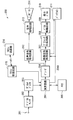
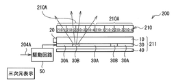
- FIG. 1 is a block diagram showing a configuration example of a transmission and reception system of a television broadcast signal 100A including a reception side apparatus 200 according to a first embodiment of the present invention.
- This transmission / reception system includes, for example, a transmission side apparatus 100 for transmitting a television broadcast signal via a wired (cable TV etc.) or wireless (terrestrial digital waves, satellite waves etc.), and a transmitting side via the above-mentioned wired or wireless
- a receiving device 200 for receiving a television broadcast signal from the device 100.
- the receiving device 200 corresponds to a specific example of the “display device” in the present invention.
- the television broadcast signal 100A includes video data for two-dimensional display (planar display) or video data for three-dimensional display (stereoscopic display).
- the video data for two-dimensional display refers to two-dimensional video data having no viewpoint information.
- video data for three-dimensional display refers to two-dimensional video data having viewpoint information
- video data for three-dimensional display includes a plurality of two-dimensional video data having different viewpoints.
- the transmission side apparatus 100 is, for example, a television broadcast signal transmission apparatus installed at a broadcast station, or a server on the Internet.
- FIG. 2 is a block diagram showing a configuration example of the reception side apparatus 200.
- the reception side device 200 is a display device capable of performing two-dimensional display and three-dimensional display, and is, for example, a television that can be connected to the above-mentioned wired or wireless.
- the receiving device 200 includes, for example, an antenna terminal 201, a digital tuner 202, a demultiplexer 203, an arithmetic circuit 204, and a memory 205.
- the receiving device 200 also includes, for example, a decoder 206, a video signal processing circuit 207, a graphic generation circuit 208, a panel drive circuit 209, a display panel 210, a backlight 211, an audio signal processing circuit 212, an audio amplification circuit 213, and a speaker. It has 214.
- the reception side apparatus 200 further includes, for example, a remote control reception circuit 215 and a remote control transmitter 216.
- the backlight 211 corresponds to a specific example of the “lighting device” in the present invention.
- the antenna terminal 201 is a terminal for inputting a television broadcast signal received by a receiving antenna (not shown).
- the digital tuner 202 processes, for example, a television broadcast signal input to the antenna terminal 201, and outputs a predetermined transport stream corresponding to the user's selected channel.
- the demultiplexer 203 is configured to extract, for example, a partial TS (Transport Stream) corresponding to the channel selected by the user from the transport stream obtained by the digital tuner 202.
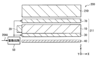
- the arithmetic circuit 204 controls the operation of each unit of the receiving device 200.
- the arithmetic circuit 204 stores, for example, the partial TS obtained by the demultiplexer 203 in the memory 205, and transmits the partial TS read from the memory 205 to the decoder 206. Further, the arithmetic circuit 204 is configured to transmit, for example, a control signal 204A for specifying two-dimensional display or three-dimensional display to the video signal processing circuit 207 and the backlight 211.
- the arithmetic circuit 204 sets the control signal 204A based on, for example, setting information stored in the memory 205, predetermined information included in the partial TS, or setting information input from the remote control reception circuit 215. It has become.
- the memory 205 stores, for example, setting information of the reception side apparatus 200 and manages data.
- the memory 205 can store, for example, partial TSs obtained by the demultiplexer 203 and setting information such as a display method.
- the decoder 206 obtains video data by performing decoding processing on a video PES (Packetized Elementary Stream) packet included in the partial TS obtained by the demultiplexer 203, for example.
- the decoder 206 is also configured to obtain audio data by performing decoding processing on an audio PES packet included in the partial TS obtained by the demultiplexer 203, for example.
- the video data refers to video data for two-dimensional display or video data for three-dimensional display.
- the video signal processing circuit 207 and the graphic generation circuit 208 perform, for example, multi-image processing, superimposing processing of graphic data, and the like on the video data obtained by the decoder 206 as necessary.
- the video signal processing circuit 207 is a case where a signal designating three-dimensional display is input from the arithmetic circuit 204 as the control signal 204A, and the video data input from the decoder 206 is video data for three-dimensional display.
- the video data input from the decoder 206 is video data for three-dimensional display.
- one two-dimensional video data is created using a plurality of two-dimensional video data with different viewpoints included in the three-dimensional display video data input from the decoder 206, and created The video data is selected as video data to be output to the graphic generation circuit 208.
- the video signal processing circuit 207 generates two two-dimensional video data in one horizontal direction.
- the process of arranging the lines alternately is performed in each row to create one image data in which two two-dimensional image data are alternately arranged in the horizontal direction.
- the video signal processing circuit 207 performs four-dimensional video data in the horizontal direction.
- the processing of periodically arranging one by one in each row is performed in each row to create one piece of video data in which four two-dimensional video data are periodically arranged one by one in the horizontal direction.
- the video signal processing circuit 207 is a case where a signal designating 2D display is input as a control signal 204A from the arithmetic circuit 204, and the video data input from the decoder 206 is video data for 3D display. For example, when there is any one of video data of a plurality of two-dimensional video data from different viewpoints included in the video data for three-dimensional display input from the decoder 206, the video is output to the graphic generation circuit 208 It is selected as data.
- the video signal processing circuit 207 is a case where a signal designating 2D display is input as a control signal 204A from the arithmetic circuit 204, and video data input from the decoder 206 is video data for 2D display. When there is, for example, video data for two-dimensional display input from the decoder 206 is selected as video data to be output to the graphic generation circuit 208.
- the graphic generation circuit 208 generates, for example, a UI (User Interface) screen used for screen display.
- the panel drive circuit 209 drives the display panel 210 based on, for example, video data output from the graphic generation circuit 208.
- the audio signal processing circuit 212 is configured to perform processing such as D / A conversion on the audio data obtained by the decoder 206, for example.
- the audio amplification circuit 213 amplifies, for example, the audio signal output from the audio signal processing circuit 212 and supplies the amplified signal to the speaker 214.
- the remote control reception circuit 215 receives, for example, the remote control signal transmitted from the remote control transmitter 216, and supplies the remote control signal to the arithmetic circuit 204.
- the arithmetic circuit 204 is configured to control each unit of the receiving device 200 according to, for example, a remote control signal.
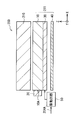
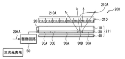
- FIG. 3 illustrates an example of the cross-sectional configuration of the receiving device 200.
- FIG. 3 is represented typically and is not necessarily the same as an actual dimension or shape.
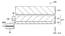
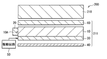
- the receiving device 200 includes a display panel 210 and a backlight 211 disposed behind the display panel 210.
- the backlight 211 corresponds to a specific example of the “lighting device” in the present invention.
- the display panel 210 is for displaying an image.
- the display panel 210 is, for example, a transmissive liquid crystal display panel (LCD (Liquid Crystal Display)) in which each pixel is driven according to a video signal, and has a structure in which a liquid crystal layer is sandwiched between a pair of transparent substrates.
- the display panel 210 includes, in order from the backlight 211 side, a polarizing plate, a transparent substrate, a pixel electrode, an alignment film, a liquid crystal layer, an alignment film, a common electrode, a color filter, a transparent substrate and a polarizing plate. have.
- the transparent substrate is made of a substrate transparent to visible light, such as a plate glass.
- an active drive circuit including TFTs (Thin Film Transistors) and wirings electrically connected to the pixel electrodes is formed on the transparent substrate on the backlight 211 side.
- the pixel electrode and the common electrode are made of, for example, ITO.
- the pixel electrodes are arranged in a lattice on a transparent substrate and function as electrodes for each pixel.
- the common electrode is formed on one surface of the color filter, and functions as a common electrode opposed to each pixel electrode.
- the alignment film is made of, for example, a polymer material such as polyimide, and performs alignment processing on the liquid crystal.
- the liquid crystal layer is made of, for example, liquid crystal in a VA (Vertical Alignment) mode, a TN (Twisted Nematic) mode or a STN (Super Twisted Nematic) mode, and an applied voltage from a driving circuit (not shown) causes the backlight 211 to It has a function of changing the direction of the polarization axis of the emitted light pixel by pixel. Note that the orientation of the transmission axis for each pixel is adjusted in multiple steps by changing the alignment of the liquid crystal in multiple steps.
- VA Vertical Alignment
- TN Transmission Nematic
- STN Super Twisted Nematic
- the color filter separates the light transmitted through the liquid crystal layer into, for example, three primary colors of red (R), green (G) and blue (B), or R, G, B and white (W)
- the color filters for color separation into four colors such as are arranged in correspondence with the arrangement of the pixel electrodes.
- the polarizing plate is a kind of optical shutter, and transmits only light (polarized light) having a certain vibration direction.
- the polarizing plate may be an absorption-type polarizing element that absorbs light (polarization) in the vibration direction other than the transmission axis, but the reflection-type polarizing element that reflects to the backlight 211 side improves the luminance. It is preferable from the viewpoint of
- the polarizing plates are arranged such that their polarization axes are different or parallel to each other by 90 degrees, so that the light emitted from the backlight 211 is transmitted or blocked through the liquid crystal layer.
- the backlight 211 is a lighting device for a display device capable of performing two-dimensional display and three-dimensional display.
- the backlight 211 illuminates the display panel 210 from behind, for example.
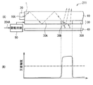
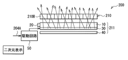
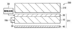
- the light guide plate 10, the light source 20 disposed on the side surface of the light guide plate 10, the light modulation element 30 disposed behind the light guide plate 10, and the reflection A plate 40 and a drive circuit 50 for driving the light modulation element 30 are provided.
- the light guide plate 10 guides the light from the light source 20 disposed on the side surface of the light guide plate 10 to the upper surface of the light guide plate 10.
- the light guide plate 10 has a shape corresponding to the display panel 210 disposed on the upper surface of the light guide plate 10, for example, a rectangular parallelepiped shape surrounded by the upper surface, the lower surface, and the side surface.
- the side surface which the light from the light source 20 injects among the side surfaces of the light-guide plate 10 shall be called the light-incidence surface 10A.
- the light guide plate 10 has, for example, a predetermined patterned shape on at least one of the upper surface and the lower surface, and has a function of scattering and homogenizing the light incident from the light incident surface 10A. There is.
- the light guide plate 10 mainly includes, for example, a transparent thermoplastic resin such as polycarbonate resin (PC) or acrylic resin (polymethyl methacrylate (PMMA)).
- PC polycarbonate resin
- PMMA polymethyl methacrylate
- the light source 20 is a linear light source, and for example, a hot cathode fluorescent lamp (HCFL; Hot Cathode Fluorescent Lamp), a cold cathode fluorescent lamp (CCFL; Cold Cathode Fluorescent Lamp), or a plurality of LEDs (Light Emitting Diodes) arranged in a row It consists of things etc.
- HCFL Hot Cathode Fluorescent Lamp
- CCFL Cold Cathode Fluorescent Lamp
- the light source 20 may be configured to include, for example, a red LED, a green LED, and a blue LED.
- the light source 20 may be provided only on one side surface of the light guide plate 10 (see FIG. 3), or may be provided on two side surfaces, three side surfaces, or all side surfaces of the light guide plate 10.
- the reflection plate 40 is for returning light leaked out from the back of the light guide plate 10 through the light modulation element 30 to the light guide plate 10 side, and has, for example, functions such as reflection, diffusion, and scattering.
- the reflection plate 40 is made of, for example, foamed PET (polyethylene terephthalate), a silver vapor deposition film, a multilayer reflective film, white PET, or the like.
- the reflecting plate 40 can be omitted as required, for example, as shown in FIG.
- the light modulation element 30 is in close contact with the back (lower surface) of the light guide plate 10 without an air layer, and for example, is bonded to the back of the light guide plate 10 via an adhesive (not shown). It is done.
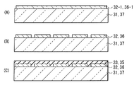
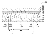
- the light modulation element 30 includes a transparent substrate 31, a lower electrode 32, an alignment film 33, a light modulation layer 34, an alignment film 35, an upper electrode 36 and a transparent substrate 37 as a reflection plate 40. It is arranged in order from the side.
- the lower electrode 32 corresponds to one specific example of the "first electrode” in the present invention
- the upper electrode 36 corresponds to one specific example of the "second electrode” in the present invention.
- the transparent substrates 31 and 37 support the light modulation layer 34 and are generally made of a substrate transparent to visible light, such as a glass plate or a plastic film.
- the lower electrode 32 is provided on the surface of the transparent substrate 31 facing the transparent substrate 37.
- the light modulation element 30 is partially extracted. It consists of a sheet of solid film formed across the surface.
- the upper electrode 36 is provided on the surface of the transparent substrate 37 facing the transparent substrate 31.
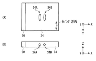
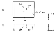
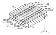
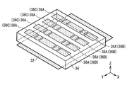
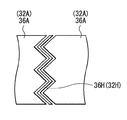
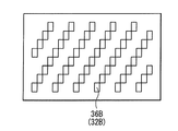
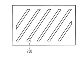
- the upper electrode 36 is constituted by a plurality of partial electrodes 36A.
- the partial electrode 36A corresponds to one specific example of the "first partial electrode" and the "second partial electrode" in the present invention.
- the plurality of partial electrodes 36A have a band shape extending in one direction in the plane (the direction parallel to the light incident surface 10A).
- the partial electrode 36B corresponds to one specific example of the "first partial electrode” in the present invention
- the partial electrode 36C corresponds to one specific example of the "second partial electrode” in the present invention.
- the plurality of partial electrodes 36 B are used to generate linear illumination light when three-dimensional display is performed in the receiving device 200.
- the plurality of partial electrodes 36B are arranged at a pitch P1 (the same pitch as the pixel pitch P2 or a pitch close thereto) corresponding to the pixel pitch P2 (see FIG. 16) when three-dimensional display is performed in the reception side device 200.
- the plurality of partial electrodes 36B and the plurality of partial electrodes 36C are alternately arranged in the arrangement direction (the direction orthogonal to the light incident surface 10A). When two-dimensional display is performed in the reception side apparatus 200, all the partial electrodes 36A are used to generate planar illumination light.
- At least the upper electrode 36 (the electrode on the upper surface side of the backlight 211) of the lower electrode 32 and the upper electrode 36 is formed of a transparent conductive film.
- the transparent conductive film preferably has, for example, the characteristics represented by the following formula (see FIG. 7A).
- the transparent conductive film is made of, for example, a film containing indium tin oxide (ITO; Indium Tin Oxide) (hereinafter referred to as "ITO film").
- ITO film indium tin oxide
- the lower electrode 32 and the upper electrode 36 may be made of indium zinc oxide (IZO), metal nanowires, carbon nanotubes, graphene or the like.
- A1-A2 ⁇ 2.00
- A1 Maximum light absorptivity (%) at 450 nm to 650 nm
- A2 Minimum light absorptivity (%) from 450 nm to 650 nm
- the difference in light absorption of the transparent conductive film be small in the range of 380 to 780 nm.
- the difference between the maximum value and the minimum value of the light absorptivity in the range of 380 to 780 nm is preferably 10.00 or less, more preferably 7.00 or less.
- the difference between the maximum value and the minimum value of the light absorptivity is preferably 2.00 or less within the range of the wavelength range of the light source used. More preferably, it is 00 or less.
- the difference between the maximum value and the minimum value of the light absorptivity is preferably 2.00 or less and 1.00 or less in the range of 450 to 650 nm. Is more preferred.
- the absorptivity is measured using V-550 manufactured by Nippon Bunko Co., and the reflectance and transmittance are measured at 5 ° incidence from the substrate normal direction, and the value of reflectance and transmittance is subtracted from 100%. It is the absorption rate.
- the transparent conductive film in the light modulation element 30 is in the process of propagating the light emitted from the light source 20 in the light guide plate 10.
- the transparent conductive film is a general ITO film, for example, as shown by the broken lines in FIGS. 7B and 7C and the arrows in FIG. 8A, the distance from the light source 20 is long. As it becomes, the component on the long wavelength side increases.
- the transparent conductive film is made of an ITO film with improved film quality, which has the characteristics shown in the above equation, it is shown, for example, in solid lines in FIGS.
- the dye includes a dye or a pigment which absorbs, for example, light on the long wavelength side more than light on the short wavelength side.
- Known materials can be used as the above-mentioned dyes and pigments.
- the formation of the light modulation layer includes a process by ultraviolet irradiation
- the light guide plate containing the dye / pigment and the light modulation element are attached to each other
- the light emitted from the light source repeatedly passes through the light modulation element in the process of propagating in the light guide plate
- the wavelength dependence of absorption of the light modulation element including the ITO film is suppressed.
- the lower electrode 32 (the electrode on the lower surface side of the backlight 211) may not be a transparent material, and may be made of, for example, a metal.
- the lower electrode 32 also has a function of reflecting light incident on the light modulation element 30 from the back of the light guide plate 10 as well as the reflection plate 40. It will be. Therefore, in this case, for example, as shown in FIG. 4, it is possible to eliminate the reflector 40.
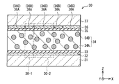
- the portion of the light modulation element 30 corresponding to the portion where the lower electrode 32 and the upper electrode 36 face each other is light
- the modulation cells 30-1 and 30-2 are configured.
- the light modulation cell 30-1 corresponds to a portion of the light modulation element 30 where the lower electrode 32 and the partial electrode 36 B face each other
- the light modulation cell 30-2 is a portion of the light modulation element 30.
- the lower electrode 32 and the partial electrode 36C correspond to portions facing each other.
- the light modulation cell 30-1 and the light modulation cell 30-2 are adjacent to each other.
- Each of the light modulation cells 30-1 and 30-2 can be independently driven by applying a predetermined voltage to the lower electrode 32 and the upper electrode 36 (partial electrode 36A).
- the light from the light source 20 exhibits transparency or scatters. The transparency and the scattering property will be described in detail when the light modulation layer 34 is described.
- the alignment films 33 and 35 align, for example, liquid crystals and monomers used in the light modulation layer 34.
- the type of alignment film for example, there are an alignment film for vertical and an alignment film for horizontal, but in the present embodiment, an alignment film for horizontal is used as the alignment films 33 and 35.
- the alignment film for horizontal use include an alignment film formed by rubbing polyimide, polyamideimide, polyvinyl alcohol and the like, and an alignment film to which a groove shape is given by transfer, etching or the like.
- the alignment film for horizontal for example, an alignment film formed by oblique deposition of an inorganic material such as silicon oxide, a diamond-like carbon alignment film formed by ion beam irradiation, and an electrode pattern slit An alignment film is mentioned.
- the baking temperature after applying the alignment films 33 and 35 on the surfaces of the transparent substrates 31 and 37 be as low as possible in the manufacturing process.
- 35 it is preferable to use a polyamideimide that can be formed at a temperature of 100 ° C. or less.
- either vertical or horizontal alignment film it is sufficient if it has a function of aligning liquid crystal and monomer, and there is no need for reliability due to repeated application of voltage required for a normal liquid crystal display.
- the reliability due to voltage application after device formation is determined by the interface between the polymerized monomer and the liquid crystal.
- the alignment film When a voltage is used to form the alignment film, separate electrodes may be formed for alignment and driving, or dual-frequency liquid crystal in which the sign of dielectric anisotropy is reversed depending on the frequency may be used as the liquid crystal material. it can.
- a magnetic field for formation of alignment film it is preferable to use the material with large magnetic susceptibility anisotropy as an alignment film, for example, it is preferable to use the material with many benzene rings.
- the light modulation layer 34 exhibits scattering or transparency to the light from the light source 20 depending on the magnitude of the electric field.
- the light modulation layer 34 is a composite layer that includes a bulk 34A and a plurality of fine particles 34B dispersed in the bulk 34A.
- the bulk 34A and the microparticles 34B have optical anisotropy.
- the bulk 34A corresponds to the "second region” in the present invention, and the fine particles 34B correspond to the "first region” in the present invention.
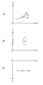
- FIG. 9A schematically shows an example of the alignment state in the microparticles 34B when no voltage is applied between the lower electrode 32 and the upper electrode 36.
- FIG. 9A the description of the orientation state in the bulk 34A is omitted.
- FIG. 9B shows an example of a refractive index ellipsoid showing refractive index anisotropy of the bulk 34A and the fine particles 34B when no voltage is applied between the lower electrode 32 and the upper electrode 36. is there.
- This refractive index ellipsoid represents the refractive index of linearly polarized light incident from various directions as a tensor ellipsoid, and by looking at the cross section of the ellipsoid from the light incident direction, the refractive index is geometrically refractive index You can know In FIG. 9C, the light modulation layer 34 transmits the light L1 directed in the front direction and the light L2 directed in the oblique direction when no voltage is applied between the lower electrode 32 and the upper electrode 36. Is schematically represented.
- FIG. 10A schematically shows an example of the alignment state in the microparticles 34B when a voltage is applied between the lower electrode 32 and the upper electrode 36.
- FIG. 10A shows an example of a refractive index ellipsoid showing refractive index anisotropy of the bulk 34A and the fine particles 34B when a voltage is applied between the lower electrode 32 and the upper electrode 36. is there.
- FIG. 10C when a voltage is applied between the lower electrode 32 and the upper electrode 36, the light L1 directed to the front direction and the light L2 directed to the oblique direction are scattered in the light modulation layer 34. It is a schematic representation of an example of the situation.
- the bulk 34A and the particles 34B are the optical axis AX1 and the particles of the bulk 34A.
- the directions of the optical axes AX2 of the lens 34B are in agreement (parallel) with each other.
- the optical axes AX1 and AX2 indicate lines parallel to the traveling direction of the light beam such that the refractive index has a single value regardless of the polarization direction.
- the directions of the optical axis AX1 and the optical axis AX2 do not have to be always coincident with each other, and the direction of the optical axis AX1 and the direction of the optical axis AX2 may be somewhat deviated due to, for example, a manufacturing error.
- the fine particles 34B are configured such that the optical axis AX2 is parallel to the light incident surface 10A of the light guide plate 10. Further, for example, when no voltage is applied between the lower electrode 32 and the upper electrode 36, the fine particles 34B are configured such that the optical axis AX2 intersects the surfaces of the transparent substrates 31 and 37 at a slight angle ⁇ 1. (See FIG. 9 (B)). The angle ⁇ 1 will be described in detail when describing the material constituting the fine particles 34B.
- the optical axis AX1 of the bulk 34A is fixed regardless of the presence or absence of voltage application between the lower electrode 32 and the upper electrode 36.
- the bulk 34 A has the light axis AX 1 of the bulk 34 A as the light incident surface of the light guide plate 10. It is configured to be parallel to 10A and to intersect the surfaces of the transparent substrates 31 and 37 at a predetermined angle ⁇ 1. That is, when no voltage is applied between the lower electrode 32 and the upper electrode 36, the optical axis AX1 of the bulk 34A is parallel to the optical axis AX2 of the particle 34B.
- the optical axis AX2 does not always need to be parallel to the light incident surface 10A of the light guide plate 10 and intersect the surfaces of the transparent substrates 31 and 37 at the angle ⁇ 1. And the angle ⁇ 1 may intersect at a slightly different angle. Further, the optical axes AX1 and AX2 need not always be parallel to the light incident surface 10A of the light guide plate 10. For example, even if they intersect with the light incident surface 10A of the light guide plate 10 at a small angle Good.
- the ordinary light refractive indexes of the bulk 34A and the fine particles 34B be equal to each other, and the extraordinary light refractive indexes of the bulk 34A and the fine particles 34B be equal to each other.
- the refractive index difference is almost all in all directions including the front direction and the oblique direction. High transparency can be obtained.
- the light L1 directed in the front direction and the light L2 directed in the oblique direction pass through the light modulation layer 34 without being scattered in the light modulation layer 34. .
- the light L from the light source 20 (light from the oblique direction) is an interface of the transparent region 30A (the transparent substrate 31 or the light guide plate 10 with air).
- the brightness (brightness of black display) of the transparent region 30A is lowered as compared with the case where the light modulation element 30 is not provided (the alternate long and short dashed line in FIG. 11B).
- the bulk 34A and the fine particle 34B have the optical axis AX1 and the optical axis AX2 oriented as shown in FIG. They are mutually different (intersect) configurations.
- the particle 34B has the optical axis AX2 of the particle 34B parallel to the light incident surface 10A of the light guide plate 10 and the transparent substrate 31,
- the surface 37 intersects with the surface 37 at an angle ⁇ 2 (eg, 90 °) larger than the angle ⁇ 1.
- the angle ⁇ 2 will be described in detail when describing the material constituting the fine particle 34B.
- the refractive index difference is large in all directions including the front direction and the oblique direction, and high scattering can be obtained.
- the light L1 directed in the front direction and the light L2 directed in the oblique direction are scattered in the light modulation layer 34.
- the light L from the light source 20 (light from the oblique direction) is the interface of the scattering region 30B (the interface between the transparent substrate 31 or the light guide plate 10 and air)
- the light transmitted to the side of the reflection plate 40 is reflected by the reflection plate 40 and is transmitted through the light modulation element 30. Therefore, the luminance of the scattering region 30B is extremely high as compared with the case where the light modulation element 30 is not provided (the alternate long and short dash line in FIG. 11B).
- the brightness (brightness boost) of typical white display is increased.
- the ordinary light refractive index of the bulk 34A and the fine particles 34B may be somewhat shifted due to, for example, a manufacturing error, and is preferably 0.1 or less, more preferably 0.05 or less. Further, the extraordinary refractive index of the bulk 34A and the fine particles 34B may be somewhat shifted due to, for example, a manufacturing error, for example, preferably 0.1 or less, and more preferably 0.05 or less.
- the difference in refractive index between the bulk 34A and the particles 34B is large, the scattering ability of the light modulation layer 34 becomes high, the light guiding condition can be easily broken, and the light from the light guide plate 10 can be easily extracted. .
- the bulk 34A and the microparticles 34B have different response speeds to the electric field.
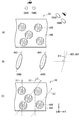
- the bulk 34A has, for example, a linear structure (see FIGS. 12A and 12B), a porous structure, or a rod-like structure having a response speed slower than that of the fine particles 34B.
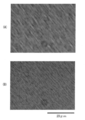
- 12 (A) and 12 (B) are polarization photomicrographs when an electric field is applied to the light modulation element 30, and in FIG. 12 (A) and FIG. Corresponds to the striated structure.
- FIG. 12 (A) shows the streak structure of the bulk 34A when the weight ratio of liquid crystal to monomer is 95: 5
- FIG. 12 (B) shows the weight ratio of liquid crystal to monomer.
- the bulk 34A is formed of, for example, a polymer material obtained by polymerizing low molecular weight monomers.
- the bulk 34A is produced, for example, by polymerizing a material having orientation and polymerization (for example, a monomer) which is oriented along the orientation direction of the fine particles 34B or the orientation direction of the orientation films 33 and 35 by at least one of heat and light. It is formed.
- the linear structure, porous structure or rod-like structure of the bulk 34A is, for example, parallel to the light incident surface 10A of the light guide plate 10 and intersects the surface of the transparent substrates 31 and 37 at a slight angle ⁇ 1.
- the average streak tissue size in the minor axis direction is 0.1 ⁇ m or more and 10 ⁇ m or less from the viewpoint of increasing the scattering property of the light guide light Is preferable, and the range of 0.2 ⁇ m or more and 2.0 ⁇ m or less is more preferable.
- the scattering ability in the light modulation element 30 becomes substantially equal in the visible region of 380 to 780 nm. Therefore, since only light of a specific wavelength component does not increase or decrease in the plane, the balance in the visible region can be balanced in the plane.
- the average muscle tissue size in the minor axis direction is less than 0.1 ⁇ m or exceeds 10 ⁇ m, the scattering ability of the light modulation element 30 is low regardless of the wavelength, and the light modulation element 30 performs light modulation It is difficult to function as an element.
- the average muscle tissue size in the minor axis direction is preferably in the range of 0.5 ⁇ m to 5 ⁇ m, and is in the range of 1 to 3 ⁇ m. Is more preferred.
- the wavelength dependence of scattering in the bulk 34A Sex is suppressed.
- the size of the muscle tissue can be observed with a polarization microscope, a confocal microscope, an electron microscope and the like.
- the fine particles 34B mainly include, for example, a liquid crystal material, and have a response speed sufficiently faster than that of the bulk 34A.
- the liquid crystal material (liquid crystal molecules) contained in the microparticles 34B is, for example, rod-like molecules.
- liquid crystal molecules contained in the fine particles 34B it is preferable to use one having positive dielectric anisotropy (so-called positive liquid crystal).
- the major axis direction of the liquid crystal molecules in the fine particle 34B is parallel to the optical axis AX1.
- the major axes of the liquid crystal molecules in the fine particles 34B are parallel to the light incident surface 10A of the light guide plate 10 and intersect the surfaces of the transparent substrates 31 and 37 at a slight angle ⁇ 1. That is, when no voltage is applied between the lower electrode 32 and the upper electrode 36, the liquid crystal molecules in the fine particles 34B are aligned in an inclined state by an angle ⁇ 1 in a plane parallel to the light incident surface 10A of the light guide plate 10. doing.
- This angle ⁇ 1 is called a pretilt angle, and is preferably in the range of, for example, 0.1 ° or more and 30 ° or less.
- the angle ⁇ 1 is more preferably in the range of 0.5 ° to 10 °, and still more preferably in the range of 0.7 ° to 2 °.
- the angle ⁇ 1 is increased, the scattering efficiency tends to decrease for the reason described later.
- the angle ⁇ 1 is too small, the rising azimuth angle of the liquid crystal at the time of voltage application varies. For example, the liquid crystal may rise in the direction opposite to 180 ° (reverse tilt). As a result, the difference in refractive index between the fine particles 34B and the bulk 34A can not be used effectively, so the scattering efficiency tends to be low and the luminance tends to be low.
- the major axis direction of the liquid crystal molecules intersect (or are orthogonal to) the optical axis AX1 in the fine particles 34B.
- the major axes of the liquid crystal molecules in the fine particles 34B are parallel to the light incident surface 10A of the light guide plate 10 and intersect the surfaces of the transparent substrates 31 and 37 at an angle ⁇ 2 (eg 90 °) larger than the angle ⁇ 1.
- any material having optical anisotropy and being composite with liquid crystal may be used, but in the present embodiment, a low molecular weight monomer cured by ultraviolet light Is preferred. Since it is preferable that the directions of optical anisotropy of the liquid crystal and those formed by polymerizing low molecular weight monomers (polymer material) coincide with each other in the state of no voltage application, before curing with ultraviolet light. Preferably, the liquid crystal and the low molecular weight monomer are aligned in the same direction.
- liquid crystal is used as the fine particles 34B, when the liquid crystal is rod-like molecules, it is preferable that the shape of the monomer material to be used is also rod-like.
- a material having both polymerizability and liquid crystallinity as the monomer material.
- a polymerizable functional group an acrylate group, a methacrylate group, an acryloyloxy group, a methacryloyloxy group, a vinyl ether group and an epoxy group
- at least one functional group selected from the group consisting of These functional groups can be polymerized by irradiation with ultraviolet light, infrared light or electron beam, or by heating.
- a liquid crystalline material having a multifunctional group can also be added in order to suppress the decrease in the degree of alignment upon irradiation with ultraviolet light.
- a bifunctional liquid crystal monomer as a raw material of the bulk 34A.
- a monofunctional monomer can be added to the raw material of the bulk 34A for the purpose of adjusting the temperature showing liquid crystallinity, or a trifunctional or higher monomer can be added for the purpose of improving the crosslink density.
- the optical axis AX2 of the particle 34B is parallel or almost parallel to the optical axis AX1 of the bulk 34A, and in the other light modulation cell 30-2, the optical axis of the particle 34B
- the magnitude of the voltage applied to the pair of electrodes (lower electrode 32 and upper electrode 36) of each of the light modulation cells 30-1 and 30-2 is controlled so that AX2 intersects or is orthogonal to the optical axis AX1 of the bulk 34A. It is supposed to be.
- the drive circuit 50 can make the directions of the optical axes AX1 and AX2 of the bulk 34A and the microparticles 34B coincide (or substantially coincide) with each other or be different (or orthogonal) with each other by electric field control. It has become.
- the drive circuit 50 is configured to cause the backlight 211 to output a plurality of linear illumination lights when a signal designating three-dimensional display is input as the control signal 204A. Specifically, the drive circuit 50 applies a voltage at which the light modulation layer 34 exhibits a scattering property to a specific plurality of partial electrodes 36B among the plurality of partial electrodes 36A, and a plurality of the plurality of partial electrodes 36A. A voltage showing transparency of the light modulation layer 34 is applied to the plurality of partial electrodes 36C except the partial electrode 36B.
- the optical axis AX2 of the fine particles 34B intersects the optical axis AX1 of the bulk 34A, and all the light modulations included in the backlight 211
- the pair of electrodes (lower electrode 32, partial electrode 36A) of each of the light modulation cells 30-1 and 30-2 such that the optical axis AX2 of the fine particles 34B is parallel to the optical axis AX1 of the bulk 34A in the cell 30-2.
- the magnitude of the voltage applied to it is controlled.
- the drive circuit 50 is configured to output planar illumination light from the backlight 211 when a signal designating two-dimensional display is input as the control signal 204A.
- the drive circuit 50 is configured to apply, to all of the plurality of partial electrodes 36A, a voltage at which the light modulation layer 34 exhibits a scattering property.
- the drive circuit 50 causes the light axis AX2 of the particles 34B to intersect the light axis AX1 of the bulk 34A.
- the magnitude of the voltage applied to the pair of electrodes 30-1 and 30-2 (lower electrode 32 and partial electrode 36 A) is controlled.
- a plane having a luminance distribution corresponding to video data from backlight 211 When a signal designating two-dimensional display is input as control signal 204A and a signal relating to video data is also input to drive circuit 50, a plane having a luminance distribution corresponding to video data from backlight 211.
- the illumination light may be configured to output planar illumination light (for example, planar illumination light in which a part of the surface is dark).
- the upper electrode 36 has a layout corresponding to the pixel of the display panel 210.
- the drive circuit 50 causes the light modulation layer 34 to exhibit the scattering property to a part of the plurality of partial electrodes 36A according to the video data.
- the light modulation layer 34 applies a voltage indicating transparency to the one or a plurality of partial electrodes 36A to which the voltage indicating the scattering property is not applied. It is supposed to
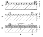
- transparent conductive films 32-1 and 36-1 such as ITO are formed on the transparent substrates 31 and 37 made of a glass substrate or a plastic film substrate (FIG. 13A).
- a resist layer is formed on the entire surface, and then an electrode pattern (lower electrode 32, upper electrode 36) is formed on the resist layer by patterning (FIG. 13B).
- patterning for example, photolithography, laser processing, pattern printing, screen printing, or the like can be used.
- patterning may be performed by screen printing using Merck's "hyper-etch" material, followed by predetermined heating, and then washing with water.
- the electrode pattern is determined by the driving method and the division number of the partial drive.
- the electrode pattern is processed, for example, at or near the pixel pitch of the display device to be used.
- the processing width of the electrode depends on the processing method, it is preferable that it be as thin as possible in terms of light extraction efficiency.
- the processing width of the electrode is, for example, 50 ⁇ m or less, preferably 20 ⁇ m, and more preferably 5 ⁇ m or less.
- an electrode pattern may be formed by firing it.
- the alignment films 33 and 35 are dried and fired (FIG. 13C).
- NMP N-methyl-2-pyrrolidone
- a temperature of about 200 ° C. is required under the atmosphere.
- the alignment films 33 and 35 can be vacuum dried at 100 ° C. and baked. Thereafter, rubbing processing is performed on the alignment films 33 and 35.
- the alignment films 33 and 35 function as alignment films for horizontal alignment, and it is possible to form a pretilt in the rubbing direction of the alignment films 33 and 35.
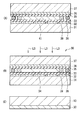
- spacers 38 for forming a cell gap are dispersed on the alignment film 33 in a dry or wet manner (FIG. 14A).
- the spacer 38 may be mixed in the mixture to be dropped.
- pillar spacers can be formed by photolithography.
- a sealing agent 39 for bonding and preventing leakage of liquid crystal is applied, for example, in a frame shape on the alignment film 35 (FIG. 14B).
- the sealant pattern 39 can be formed by a dispenser method or a screen printing method.
- the vacuum bonding method (One Drop Fill method, ODF method) will be described below, but it is also possible to form the light modulation cell 30-1 by a vacuum injection method, a roll bonding method, or the like.
- a mixture 41 of liquid crystal and monomer corresponding to volume determined by the cell gap, cell area, etc. is dropped uniformly on the surface (FIG. 14 (C)).
- a die coater or the like may be used by using the sealant pattern 39 as a bank.
- the liquid crystal and the monomer can use the above-mentioned materials, but the weight ratio of the liquid crystal to the monomer is 98: 2 to 50:50, preferably 95: 5 to 75:25, more preferably 92: 8 to 85:15. is there.
- the driving voltage can be lowered by increasing the ratio of liquid crystal, but if the amount of liquid crystal is too large, the whiteness at the time of voltage application decreases, the response speed decreases after the voltage is turned off, etc. There is a tendency to
- a polymerization initiator is added to the mixture 41.
- the monomer ratio of the polymerization initiator to be added is adjusted in the range of 0.1 to 10% by weight.
- a polymerization inhibitor, a plasticizer, a viscosity modifier and the like can be added to the mixture 41 as necessary.
- the monomer is solid or gel at room temperature, it is preferable to heat the nozzle, the syringe, or the substrate.
- the cell gap can be appropriately selected from the relationship between white luminance (whiteness) and driving voltage, but is 5 to 40 ⁇ m, preferably 6 to 20 ⁇ m, and more preferably 7 to 10 ⁇ m.
- the light modulation element 30 is manufactured.
- the temperature of the cell it is preferable to keep the temperature of the cell unchanged when irradiating with ultraviolet light. It is preferable to use an infrared cut filter or to use a UV-LED as a light source. Since the ultraviolet light intensity affects the structure of the composite material, it is preferably adjusted appropriately from the liquid crystal material and monomer material to be used, and their composition, preferably in the range of 0.1 to 500 mW / cm 2 , more preferably 0. 5 to 30 mW / cm 2 . The driving voltage tends to be lower as the ultraviolet illumination intensity is lower, and a preferable ultraviolet illumination intensity can be selected from both of productivity and characteristics.
- the light modulation element 30 is attached to the light guide plate 10.
- any of adhesion and adhesion may be used, but adhesion and adhesion using a material having a refractive index as close as possible to the refractive index of the light guide plate 10 and the refractive index of the substrate material of the light modulation element 30 are preferable.
- lead wires (not shown) are attached to the lower electrode 32 and the upper electrode 36.
- the transparent substrate 37 having the alignment film 35 formed on the surface of the light guide plate 10 is attached in advance. It is also possible to create the backlight 211 after the combination.
- the backlight 211 can be formed by any of the single wafer method and the roll to roll method.
- each light modulation cell 30-1 in each light modulation cell 30-1, the optical axis AX2 of the fine particle 34B intersects or is orthogonal to the optical axis AX1 of the bulk 34A, and each light modulation cell 30- 2 so that the optical axis AX2 of the fine particles 34B is parallel or almost parallel to the optical axis AX1 of the bulk 34A, the pair of electrodes of the light modulation cells 30-1 and 30-2 (lower electrode 32, partial electrode 36A) Voltage is applied to the Thereby, in the light modulation element 30, each light modulation cell 30-1 becomes a scattering region 30B, and each light modulation cell 30-2 becomes a transmission region 30A.
- the light emitted from the light source 20 and incident into the light guide plate 10 is transmitted through the transmission region 30A of the light modulation element 30 and scattered in the scattering region 30B of the light modulation element 30 (FIG. 11).
- the scattered light light transmitted through the lower surface of the scattering region 30B is reflected by the reflecting plate 40, returned again to the light guide plate 10, and then emitted from the upper surface of the backlight 211.
- light traveling toward the upper surface of the scattering region 30B is emitted from the upper surface of the backlight 211 after transmitting through the light guide plate 10.
- each linear illumination light output in the front direction is incident on the back surface of the display panel 210.
- each pixel row corresponds to the three-dimensional pixel 210A in the pixel array corresponding to each linear illumination light.
- pixels at a common position in each of the three-dimensional pixels 210A for example, 210-1, 210-2, and 210 in FIG. 16.
- Each linear illumination light is incident at substantially the same angle on ⁇ 3 or 210-4).
- the video light modulated by the pixels is output at a predetermined angle.
- the observer since the observer observes images of parallax different from each other with the left and right eyes, the observer recognizes that the display panel 210 displays a three-dimensional image (stereoscopic image).
- the optical axis AX2 of the fine particle 34B intersects or is orthogonal to the optical axis AX1 of the bulk 34A.
- a voltage is applied to the pair of electrodes (lower electrode 32 and partial electrode 36A) of each of the light modulation cells 30-1 and 30-2.
- light emitted from the light source 20 and incident into the light guide plate 10 is scattered in the scattering region 30B formed in the entire light modulation element 30 (FIG. 17).
- planar illumination light output in the front direction is incident on the back surface of the display panel 210.
- two-dimensional video data for two-dimensional display is generated by the video signal processing circuit 207 corresponding to each pixel 210B.
- planar illumination light enters each pixel 210B at all angles, and image light modulated by each pixel 210B is output from each pixel 210B.
- the observer since the observer observes the same image with both eyes, the observer recognizes that the two-dimensional image (planar image) is displayed on the display panel 210.
- the present embodiment there is no need to provide a parallax barrier at the time of three-dimensional display. Further, even if the parallax barrier is provided on the light emission side of the backlight 211, the light modulation layer 34 outputs light only at that time, so each linear shape output from the light modulation layer 34 The rate at which the illumination light is absorbed by the parallax barrier is very low. Further, in the present embodiment, since a cylindrical lens is not required for three-dimensional display, there is no possibility that the problem of aberration due to the cylindrical lens will occur.
- a plurality of linear illumination lights are output from the backlight 211 by using a part of the light modulation element 30 as a scattering region, so display in three-dimensional display Both brightness and display quality can be improved.
- PDLC is formed by mixing a liquid crystal material and an isotropic low molecular weight material and causing phase separation by ultraviolet irradiation, drying of a solvent, etc., and fine particles of the liquid crystal material are dispersed in a polymer material.
- a composite layer has become a composite layer.
- the liquid crystal material in this composite layer exhibits a scattering property since it is randomly oriented when no voltage is applied, but it is oriented in the electric field direction when a voltage is applied, so the ordinary light refractive index of the liquid crystal material and the refractive index of the polymer material When and are equal to each other, they exhibit high transparency in the front direction (normal direction of PDLC).
- a light modulation element using PDLC often has a structure in which PDLC is sandwiched between two glass plates having a transparent conductive film formed on the surface.
- the light incident from the oblique direction is refracted due to the refractive index difference between the air and the glass plate, and the light is incident at a smaller angle. It will be incident on PDLC. Therefore, large scattering does not occur in such a light modulation element. For example, when light is incident from the air at an angle of 80 °, the incident angle of the light to the PDLC is reduced to about 40 ° by refraction at the glass interface.
- the front direction (the normal direction of PDLC)
- the refractive index difference is large in the oblique direction.
- the scattering in the oblique direction can not be reduced, the viewing angle characteristics are poor.
- an optical film such as a diffusion film is provided on the light guide plate, the obliquely leaked light is also diffused in the front direction by the diffusion film or the like, so the light leakage in the front direction becomes large and the modulation ratio in the front direction becomes lower.
- the bulk 34A and the fine particles 34B are formed mainly containing the optically anisotropic material, the scattering property is reduced in the oblique direction, and the transparency can be improved.
- the bulk 34A and the microparticles 34B mainly include optical anisotropic materials having the same ordinary refractive index and the same extraordinary refractive index, and a voltage between the lower electrode 32 and the upper electrode 36. In the region where is not applied, the directions of these optical axes coincide or almost coincide. As a result, the refractive index difference decreases or disappears in all directions including the front direction (the normal direction of the light modulation element 30) and the oblique direction, and high transparency can be obtained. As a result, light leakage in a large range of viewing angles can be reduced or almost eliminated, and viewing angle characteristics can be improved.
- a liquid crystal having ordinary light refractive index 1.5 and extraordinary light refractive index 1.65 and a liquid crystalline monomer having ordinary light refractive index 1.5 and extraordinary light refractive index 1.65 are mixed, and the liquid crystal
- the liquid crystalline monomer is polymerized in a state in which the liquid crystalline monomer is aligned, the optical axis of the liquid crystal and the optical axis of the polymer formed by the polymerization of the liquid crystalline monomer coincide with each other.
- the refractive index can be matched in all directions, and in such a case, the state of high transparency can be realized, and the viewing angle characteristics can be further improved.
- the luminance push-up is a technique for increasing the luminance when white display is performed partially as compared to the case where the entire screen is displayed white.
- This is a commonly used technology for CRTs and PDPs.
- the backlight since the backlight emits light uniformly throughout the image regardless of the image, it is not possible to partially increase the luminance.
- the backlight is an LED backlight in which a plurality of LEDs are two-dimensionally arranged, it is possible to partially turn off the LEDs.
- the luminance becomes lower than in the case where all the LEDs are turned on.
- It is also possible to increase the luminance by increasing the current supplied to the partially lit LED, but in such a case, a large current flows in a very short time. Problems remain in terms of circuit load and reliability.
- the bulk 34A and the fine particles 34B are formed mainly containing the optically anisotropic material, scattering in the oblique direction is suppressed, and light leaked from the light guide plate in the dark state is generated. Few. As a result, since light is guided from the partial dark state part to the partial bright state part, it is possible to realize the luminance boost without increasing the input power to the backlight 211.
- the optical axis AX2 of the particles 34B is parallel to the light incident surface 10A of the light guide plate 10 in a region where a voltage is not applied between the lower electrode 32 and the upper electrode 36. And, it intersects the surfaces of the transparent substrates 31 and 37 at a slight angle ⁇ 1. That is, the liquid crystal molecules contained in the fine particles 34B are aligned in a state in which the liquid crystal molecules are inclined by an angle ⁇ 1 (in a state where a pretilt angle is given) in a plane parallel to the light incident surface 10A.
- the liquid crystal material contained in the fine particles 34B does not rise in a random orientation, but in a plane parallel to the light incident surface 10A.
- the optical axes AX1 and AX2 of the bulk 34A and the fine particles 34B intersect or are orthogonal to each other in a plane parallel to the light incident surface 10A.
- the light vibrating perpendicularly to the transparent substrate 31 feels the difference between the extraordinary refractive index of the fine particles 34B and the ordinary refractive index of the bulk 34A. .
- light propagating in a region where a voltage is applied between the lower electrode 32 and the upper electrode 36 contains a large amount of oblique components.
- an acrylic light guide plate is used as the light guide plate 10
- light in a region to which a voltage is applied between the lower electrode 32 and the upper electrode 36 propagates at an angle of 41.8 ° or more.
- the refractive index difference is large in all directions including the oblique direction, and high scattering can be obtained, so that the display brightness can be improved.
- the display luminance can be further improved by the effect of the above-mentioned luminance boost.
- the optical axes AX1 and AX2 of the bulk 34A and the fine particles 34B are disposed perpendicularly to the light incident surface 10A of the light guide plate 10, and a voltage is applied between the lower electrode 32 and the upper electrode 36
- the liquid crystal material contained in the fine particles 34B is made to rise in a plane perpendicular to the light incident surface 10A, the light vibrating perpendicularly to the transparent substrate 31 is the same as the case described above.
- the light vibrating in a direction parallel to the transparent substrate 31 has the ordinary light refractive index of the fine particles 34B and the ordinary refractive index of the bulk 34A. I will feel the difference.
- the scattering efficiency of light oscillating vertically to the transparent substrate 31 is high, but the scattering efficiency of light oscillating parallel to the transparent substrate 31 is low or zero. Therefore, when the optical axes AX1 and AX2 are disposed perpendicularly to the light incident surface 10A, the scattering efficiency is lower than when the optical axes AX1 and AX2 are disposed parallel to the light incident surface 10A. Therefore, the luminance that can be extracted from the light guide plate 10 is lower than that of the light modulation element 30 of the present embodiment.
- the present embodiment it is possible to improve the display luminance while reducing or almost eliminating the light leakage in the range where the viewing angle is large. As a result, the modulation ratio in the front direction can be increased.
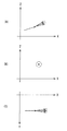
- FIG. 18 and FIG. 19 show an example of the refractive index ellipsoid of the bulk 34A and the fine particle 34B in the light modulation layer 34 of the above embodiment.
- FIG. 18 shows an example of a refractive index ellipsoid of the bulk 34A and the fine particles 34B when no voltage is applied between the lower electrode 32 and the upper electrode 36
- FIG. 19 shows the lower electrode 32.
- refractive index ellipsoids of the bulk 34A and the fine particles 34B when a voltage is applied between the upper electrodes 36 is applied between the upper electrodes 36.
- the optical axis of the bulk 34A and the optical axis of the particles 34B are incident on the light incident on the light guide plate 10. It is directed in a direction parallel to the surface 10A and in a direction intersecting the surfaces of the transparent substrates 31 and 37 at an angle ⁇ 1.
- the optical axis of the bulk 34A is between the lower electrode 32 and the upper electrode 36. It is in the same direction as when no voltage is applied.
- the optical axis of the fine particles 34B is parallel to the light incident surface 10A of the light guide plate 10 and directed to intersect the surfaces of the transparent substrates 31 and 37 at an angle ⁇ 2 (eg, 90 °) larger than the angle ⁇ 1. .
- the bulk 34A does not respond to the voltage change or the bulk 34A
- the long axis direction of the stripe-like structure of the bulk 34A is in the rubbing direction (direction parallel to the light incident surface 10A (Y-axis direction in FIGS. 18 and 19)). Therefore, when a voltage is applied between the lower electrode 32 and the upper electrode 36, the light which is output from the light source 20 and propagates in the light modulation layer 34 is an average of the short axis direction of the stripe-like structure of the bulk 34A.
- the light propagating in the light modulation layer 34 is largely scattered in the thickness direction of the light modulation layer 34 and is not largely scattered in the direction parallel to the light incident surface 10A. That is, in the light modulation layer 34, the scattering property is anisotropic in the Y-axis direction and the Z-axis direction in a plane (YZ plane) parallel to the light incident surface 10A.
- the light modulation layer 34 exhibits anisotropic scattering with respect to light that is output from the light source 20 and propagates in the light modulation layer 34.
- the light modulation layer 34 when considered from the refractive index ellipsoid of the bulk 34A and the fine particles 34B, light propagating in the Z-axis direction in FIG. 19 is in the Y-axis direction (rubbing direction) compared to the polarization component in the X-axis direction.
- the polarization component has higher scattering power. That is, the light modulation layer 34 exhibits anisotropic scattering in the polarization direction with respect to light propagating in the thickness direction of the light modulation layer 34.
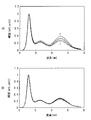
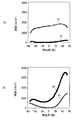
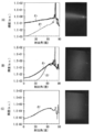
- FIGS. 20A and 20B show the results of measuring the emission angle characteristics of light from the light guide plate.
- FIG. 20 (A) shows the result when the modulation layer 34 is used
- FIG. 20 (B) shows the result when the light modulation layer showing optical isotropy in the plane. It is shown.
- a white reflector is used on the lower surface of the light modulation layer, but a black absorbing layer is used on the lower surface of the light modulation layer instead of the white reflector to accurately know the emission characteristics from the light modulation layer and the light guide plate. Placed.
- the amount of the component is large. Since the two light modulation layers used in the verification differ in the monomer material and liquid crystal material used, it is difficult to compare these two light extraction intensities themselves, but a material having the same optical properties as the light modulation layer is used In such a case, using the light modulation layer 34 having optical anisotropy in the plane can increase the utilization efficiency of light.
- the scattering characteristics of the light modulation layer 34 itself were measured.
- the matching oil 110 and the light modulation layer 34 are put in the cylindrical glass container 100, and the modulation layer 34 is irradiated with the laser light L at a large incident angle ⁇ (for example, 80 degrees) that guides light in the light guide plate. Then, the angular characteristics of the scattering were evaluated.
- ⁇ for example, 80 degrees
- FIG. 22A shows the state of the luminance distribution projected on the measurement surface 130 when the laser light L is made incident on the light modulation layer 34 at a large incident angle ⁇ (for example, 80 degrees). Furthermore, at this time, in a plane perpendicular to the rubbing direction (corresponding to the ZX plane in FIG. 18 and FIG. 19), it is parallel to the optical axis AX1 (not shown) of the bulk 34A in the light modulation layer 34.
- the light intensity distribution obtained when the detector 120 is scanned with the axis as the central axis is shown in FIG. The light intensity distribution at this time corresponds to the distribution in the direction (1) of FIG.
- the light modulation layer 34 A luminance distribution obtained when the detector 120 is scanned with the central axis being an axis orthogonal to the optical axis AX1 (not shown) of the bulk 34A is shown in FIG.
- the light intensity distribution at this time corresponds to the distribution in the direction (2) of FIG.
- the in-plane (corresponding to the ZX plane in FIG. 18 and FIG. 19) perpendicular to the rubbing direction is in-plane parallel to the rubbing direction (FIG. 18).
- the scattering characteristics are higher than in the ZY plane of FIG. 19), and the intensity is different by about 50 times in the front direction (exit angle 0 °) (during voltage application). That is, in the light modulation layer 34, for example, as shown in FIGS. 22A to 22C, scattering in the thickness direction (Z-axis direction) of the light modulation layer 34 is in the rubbing direction (light incident surface 10A). It is found that it has anisotropic scattering properties larger than scattering in the direction parallel to (Y direction).
- the liquid crystal in the particles 34B in a state where the long axis direction of the stripe-like structure of the bulk 34A is directed to the rubbing direction (direction parallel to the light incident surface 10A (Y axis direction in FIG. 18 and FIG. 19)).
- the light modulation layer 34 exhibits the above-mentioned anisotropic scattering with respect to the light emitted from the light source 20.
- FIG. 23A shows the scattering characteristic of the light modulation layer 34.
- FIG. 23B shows the scattering characteristics of the light modulation layer in which the liquid crystal is inclined by the voltage (the pretilt is 90 degrees).
- FIG. 23C shows the scattering characteristics of the normal light modulation layer having in-plane optical anisotropy using an isotropic polymer. As shown in FIGS. 23A to 23C, in the light modulation layer 34, the incident light is largely scattered in the front direction as compared with the other light modulation layers, and only the light modulation layer 34 is anisotropically scattered. It turned out that it shows.
- the reason why the light extraction from the light guide plate is excellent when such anisotropic scattering is exhibited will be described.
- the light guide plate on which the white pattern is printed and the above-mentioned normal light modulation layer are isotropic as shown in FIGS. 24 (A) to (C).
- the incident light is, for example, in the direction perpendicular to the in-plane direction of the light guide plate as shown in FIGS.
- the average streaky tissue size in the minor axis direction of the bulk 34A is preferably 0.1 ⁇ m to 10 ⁇ m, and more preferably 0.2 ⁇ m to 2 ⁇ m. More preferably, it is in the range of not more than 0 ⁇ m.
- a backlight according to a second embodiment of the present invention will be described.
- alignment films for vertical use are used as the alignment films 33 and 35, and in addition, a light modulation layer 64 is provided in place of the light modulation layer 34 of the above embodiment. It differs from the configuration of the backlight 211 of the above embodiment. So, below, the explanation about the common point with the composition of the above-mentioned embodiment is omitted suitably, and the difference with the composition of the above-mentioned embodiment is mainly explained.
- a vertical alignment film is used as the alignment films 33 and 35.
- the vertical alignment film forms a pretilt in which a bulk 64A and fine particles 64B described later are inclined from the transparent substrate 31.
- the alignment film for vertical it is possible to use a silane coupling material, polyvinyl alcohol (PVA), a polyimide-based material, a surfactant or the like. For example, by performing rubbing after coating and drying these materials, a pretilt is formed in the rubbing direction.
- PVA polyvinyl alcohol
- a polyimide-based material a surfactant or the like.
- the baking temperature after applying the alignment films 33 and 35 on the surfaces of the transparent substrates 31 and 37 be as low as possible in the manufacturing process.
- the alignment films 33 and 35 may be pre-tilted without rubbing treatment.
- a method of realizing it for example, there is a method of forming cells in the alignment films 33 and 35 and irradiating the cells with ultraviolet light while applying an oblique electric field by a magnetic field or a slit electrode.
- the light modulation layer 64 is a composite layer including a bulk 64A and a plurality of fine particles 64B dispersed in the bulk 64A, as in the above embodiment.
- the bulk 64A and the microparticles 64B have optical anisotropy.
- FIG. 26A schematically shows an example of the alignment state in the particles 64B when a voltage is not applied between the lower electrode 32 and the upper electrode 36.
- FIG. 26A shows the description of the orientation state in the bulk 64A is omitted.
- FIG. 26B shows an example of a refractive index ellipsoid showing refractive index anisotropy of the bulk 64A and the fine particles 64B when a voltage is not applied between the lower electrode 32 and the upper electrode 36. is there.
- 26C shows that the light L1 directed in the front direction and the light L2 directed in the oblique direction pass through the light modulation layer 64 when no voltage is applied between the lower electrode 32 and the upper electrode 36. Is schematically represented.
- FIG. 27A schematically shows an example of the alignment state in the particles 64B when a voltage is applied between the lower electrode 32 and the upper electrode 36.
- FIG. 27A shows an example of a refractive index ellipsoid showing refractive index anisotropy of the bulk 64A and the fine particles 64B when a voltage is applied between the lower electrode 32 and the upper electrode 36. is there.
- FIG. 27C when a voltage is applied between the lower electrode 32 and the upper electrode 36, the light L1 directed in the front direction and the light L2 directed in the oblique direction are scattered in the light modulation layer 64. It is a schematic representation of an example of the situation.
- the bulk 64A and the particles 64B are the optical axis AX3 of the bulk 64A and the particles.
- the orientations of the optical axes AX4 of 64B are in agreement (parallel) with each other.
- the optical axes AX3 and AX4 indicate lines parallel to the traveling direction of the light beam such that the refractive index has one value regardless of the polarization direction.
- the directions of the optical axis AX3 and the optical axis AX4 do not have to be always consistent with each other, and the direction of the optical axis AX3 and the direction of the optical axis AX4 may be somewhat shifted due to, for example, a manufacturing error.
- the optical axis AX4 is parallel to the light incident surface 10A of the light guide plate 10 when a voltage is not applied between the lower electrode 32 and the upper electrode 36. Further, for example, when no voltage is applied between the lower electrode 32 and the upper electrode 36, the fine particles 64B are configured such that the optical axis AX4 intersects the normal to the transparent substrates 31 and 37 at a slight angle ⁇ 3. (See FIG. 26 (B)). The angle ⁇ 3 will be described in detail when describing the material constituting the fine particle 64B.
- the optical axis AX4 of the bulk 64A is constant regardless of the presence or absence of voltage application between the lower electrode 32 and the upper electrode 36.
- the bulk 64A has the optical axis AX3 of the bulk 64A as the light incident surface of the light guide plate 10. It is configured to be parallel to 10A and to intersect the normals of the transparent substrates 31 and 37 at a slight angle ⁇ 3. That is, when no voltage is applied between the lower electrode 32 and the upper electrode 36, the optical axis AX3 of the bulk 64A is parallel to the optical axis AX4 of the particle 64B.
- optical axis AX4 it is not necessary that the optical axis AX4 always be parallel to the light incident surface 10A of the light guide plate 10 and intersect the normal lines of the transparent substrates 31 and 37 at the angle ⁇ 3.
- the normal of 37 and the angle ⁇ 3 may intersect at a slightly different angle.
- the optical axes AX3 and AX4 need not always be parallel to the light incident surface 10A of the light guide plate 10. For example, even if they intersect with the light incident surface 10A of the light guide plate 10 at a small angle Good.
- the ordinary light refractive indexes of the bulk 64A and the fine particles 64B be equal to each other, and the extraordinary light refractive indexes of the bulk 64A and the fine particles 64B be equal to each other.
- the refractive index difference is almost all in all directions including the front direction and the oblique direction. High transparency can be obtained.
- the light L1 directed in the front direction and the light L2 directed in the oblique direction pass through the light modulation layer 64 without being scattered in the light modulation layer 64. .
- the light L (light from the oblique direction) from the light source 20 is an interface of the transparent region 30A (transparent substrate 31 or at the interface between the light guide plate 10 and air), the brightness (brightness of black display) of the transparent region 30A is the case where the light modulation element 30 is not provided (dotted line in FIG. 11B) Lower by comparison.
- the bulk 64A and the fine particle 64B have the optical axis AX3 and the optical axis AX4 oriented as shown in FIG. They are mutually different (intersect) configurations.
- the particle 64B has the optical axis AX4 of the particle 64B parallel to the light incident surface 10A of the light guide plate 10 and the transparent substrate 31, It intersects with the normal line 37 at an angle ⁇ 4 larger than the angle ⁇ 3 or is parallel to the surfaces of the transparent substrates 31 and 37.
- the angle ⁇ 4 will be described in detail when describing the material constituting the fine particle 64B.
- the light propagating in the area in which the voltage is applied between the lower electrode 32 and the upper electrode 36 contains many oblique components.
- an acrylic light guide plate is used as the light guide plate 10
- light in a region to which a voltage is applied between the lower electrode 32 and the upper electrode 36 propagates at an angle of 41.8 ° or more.
- the difference in refractive index is large, and high scattering can be obtained.
- the light L1 directed in the front direction and the light L2 directed in the oblique direction are scattered in the light modulation layer 64.
- the light L (light from the oblique direction) from the light source 20 is transmitted through the interface (transparent substrate) of the scattering region 30B. 31 or the interface between the light guide plate 10 and the air), and the light transmitted to the side of the reflection plate 40 is reflected by the reflection plate 40 and is transmitted through the light modulation element 30. Therefore, the luminance of the scattering region 30B is extremely high as compared with the case where the light modulation element 30 is not provided (the alternate long and short dash line in FIG. 11B).
- the brightness (brightness boost) of typical white display is increased.
- the ordinary light refractive indexes of the bulk 64A and the fine particles 64B may be somewhat shifted due to, for example, a manufacturing error, and for example, 0.1 or less is preferable and 0.05 or less is more preferable.
- the extraordinary refractive index of the bulk 64A and the fine particles 64B may be somewhat shifted due to, for example, a manufacturing error, and for example, 0.1 or less is preferable and 0.05 or less is more preferable.
- the difference in refractive index between the bulk 64A and the particles 64B is large, the scattering ability of the light modulation layer 64 is high, the light guiding condition can be easily broken, and the light from the light guide plate 10 can be easily extracted. .
- the bulk 64A and the microparticles 64B have different response speeds to the electric field.
- the bulk 64A has, for example, a linear structure or a porous structure that does not respond to an electric field, or a rod-like structure that has a response speed slower than that of the fine particles 64B.
- the bulk 64A is formed of, for example, a polymer material obtained by polymerizing low molecular weight monomers.
- the bulk 64A is produced, for example, by polymerizing a material having orientation and polymerization (for example, a monomer) which is oriented along the orientation direction of the fine particles 64B or the orientation direction of the orientation films 33 and 35 by at least one of heat and light. It is formed.
- the fine particles 64B mainly include, for example, a liquid crystal material, and have a response speed sufficiently faster than that of the bulk 64A.
- the liquid crystal material (liquid crystal molecules) contained in the fine particles 64B is, for example, rod-like molecules.
- liquid crystal molecules contained in the fine particles 64B those having negative dielectric constant anisotropy (so-called negative liquid crystals) are used.
- the major axis direction of the liquid crystal molecules in the particle 64B is parallel to the optical axis AX3.
- the major axes of the liquid crystal molecules in the fine particles 64B are parallel to the light incident surface 10A of the light guide plate 10 and intersect the normals of the transparent substrates 31 and 37 at a slight angle ⁇ 3. That is, when no voltage is applied between the lower electrode 32 and the upper electrode 36, the liquid crystal molecules in the fine particles 64B are aligned in an inclined state at an angle ⁇ 3 in a plane parallel to the light incident surface 10A of the light guide plate 10. doing.
- the angle ⁇ 3 is called a pretilt angle, and is preferably in the range of, for example, 0.1 ° to 30 °.
- the angle ⁇ 3 is more preferably in the range of 0.5 ° to 10 °, and still more preferably in the range of 0.7 ° to 2 °. If the angle ⁇ 3 is reduced, the scattering efficiency tends to decrease for the reason described later.
- the angle ⁇ 3 is too large (for example, approximately 90 °), the falling azimuth angle of the liquid crystal varies when a voltage is applied. For example, the liquid crystal may fall in the direction opposite to 180 ° (reverse tilt). As a result, the difference in refractive index between the fine particles 64B and the bulk 64A can not be used effectively, so the scattering efficiency tends to be low and the luminance tends to be low.
- the major axis direction of the liquid crystal molecules in the fine particle 64B intersects (or is orthogonal to) the optical axis AX3.
- any material having optical anisotropy and being composite with liquid crystal may be used, but in the present embodiment, a low molecular weight monomer cured by ultraviolet light Is preferred. Since it is preferable that the directions of optical anisotropy of the liquid crystal and those formed by polymerizing low molecular weight monomers (polymer material) coincide with each other in the state of no voltage application, before curing with ultraviolet light. Preferably, the liquid crystal and the low molecular weight monomer are aligned in the same direction.
- liquid crystal is used as the fine particles 64B, when the liquid crystal is rod-like molecules, it is preferable that the shape of the monomer material to be used is also rod-like.
- a material having both polymerizability and liquid crystallinity as the monomer material.
- a polymerizable functional group an acrylate group, a methacrylate group, an acryloyloxy group, a methacryloyloxy group, a vinyl ether group and an epoxy group
- at least one functional group selected from the group consisting of These functional groups can be polymerized by irradiation with ultraviolet light, infrared light or electron beam, or by heating.
- a liquid crystalline material having a multifunctional group can also be added in order to suppress the decrease in the degree of alignment upon irradiation with ultraviolet light.
- a bifunctional liquid crystal monomer as a raw material of the bulk 64A.
- a monofunctional monomer can be added to the bulk 64A raw material for the purpose of adjusting the temperature showing liquid crystallinity, or a trifunctional or higher monomer can be added for the purpose of improving the crosslink density.
- the pair of electrodes of the light modulation cells 30-1 and 30-2 (lower electrode 32, partial electrode 36A) Voltage is applied to the Thereby, the light emitted from the light source 20 and incident into the light guide plate 10 is transmitted through the transmission region 30A in the light modulation element 30 in which the optical axis AX3 and the optical axis AX4 are parallel or substantially parallel to each other.
- the light emitted from the light source 20 and incident into the light guide plate 10 is scattered in the light modulation element 30 in the scattering region 30B in which the optical axis AX3 and the optical axis AX4 intersect or are orthogonal to each other (see FIG. 11).
- the scattered light light transmitted through the lower surface of the scattering region 30B is reflected by the reflecting plate 40, returned again to the light guide plate 10, and then emitted from the upper surface of the backlight 211.
- light traveling toward the upper surface of the scattering region 30B is emitted from the upper surface of the backlight 211 after transmitting through the light guide plate 10.
- each linear illumination light output in the front direction is incident on the back surface of the display panel 210.
- each pixel row corresponds to the three-dimensional pixel 210A in the pixel array corresponding to each linear illumination light.
- pixels at a common position in each of the three-dimensional pixels 210A for example, 210-1, 210-2, and 210 in FIG. 16.
- Each linear illumination light is incident at substantially the same angle on ⁇ 3 or 210-4).
- the video light modulated by the pixels is output at a predetermined angle.
- the observer since the observer observes images of parallax different from each other with the left and right eyes, the observer recognizes that the display panel 210 displays a three-dimensional image (stereoscopic image).
- the optical axis AX4 of the fine particle 64B intersects or is orthogonal to the optical axis AX3 of the bulk 64A.
- a voltage is applied to the pair of electrodes (lower electrode 32 and partial electrode 36A) of each of the light modulation cells 30-1 and 30-2.
- light emitted from the light source 20 and incident into the light guide plate 10 is scattered in the scattering region 30B formed in the entire light modulation element 30 (FIG. 17).
- planar illumination light output in the front direction is incident on the back surface of the display panel 210.
- two-dimensional video data for two-dimensional display is generated by the video signal processing circuit 207 corresponding to each pixel 210B.
- planar illumination light enters each pixel 210B at all angles, and image light modulated by each pixel 210B is output from each pixel 210B.
- the observer since the observer observes the same image with both eyes, the observer recognizes that the two-dimensional image (planar image) is displayed on the display panel 210.
- the light modulation layer 64 outputs light only in a linear manner at that time, and therefore each linear light output from the light modulation layer 64 The rate at which the illumination light is absorbed by the parallax barrier is very low. Further, in the present embodiment, since a cylindrical lens is not required for three-dimensional display, there is no possibility that the problem of aberration due to the cylindrical lens will occur.
- a plurality of linear illumination lights are output from the backlight 211 by using a part of the light modulation element 30 as a scattering region, so display in three-dimensional display Both brightness and display quality can be improved.
- the bulk 64A and the fine particles 64B are formed mainly containing the optical anisotropic material, the scattering property is reduced in the oblique direction, and the transparency can be improved.
- the bulk 64A and the fine particle 64B mainly include optical anisotropic materials having the same ordinary refractive index and the same extraordinary refractive index, and the voltage between the lower electrode 32 and the upper electrode 36 In the region where is not applied, the directions of these optical axes coincide or almost coincide.
- the refractive index difference decreases or disappears in all directions including the front direction (the normal direction of the light modulation element 30) and the oblique direction, and high transparency can be obtained.
- light leakage in a large range of viewing angles can be reduced or almost eliminated, and viewing angle characteristics can be improved.
- a liquid crystal having ordinary light refractive index 1.5 and extraordinary light refractive index 1.65 and a liquid crystalline monomer having ordinary light refractive index 1.5 and extraordinary light refractive index 1.65 are mixed, and the liquid crystal
- the liquid crystalline monomer is polymerized in a state in which the liquid crystalline monomer is aligned, the optical axis of the liquid crystal and the optical axis of the polymer formed by the polymerization of the liquid crystalline monomer coincide with each other.
- the refractive index can be matched in all directions, and in such a case, the state of high transparency can be realized, and the viewing angle characteristics can be further improved.
- the bulk 64A and the fine particles 64B are mainly formed including the optically anisotropic material, the scattering in the oblique direction is suppressed, and the leakage light from the light guide plate in the dark state is small. Therefore, since the light is guided from the partial dark state part to the partial bright state part, luminance boost can be realized without increasing the power input to the backlight.
- the optical axis AX4 of the fine particles 64B is parallel to the light incident surface 10A of the light guide plate 10 in a region where a voltage is not applied between the lower electrode 32 and the upper electrode 36. And it intersects with the normal of the transparent substrates 31 and 37 at a slight angle ⁇ 3. That is, the liquid crystal molecules contained in the fine particles 64B are aligned in a state in which the liquid crystal molecules are inclined by an angle ⁇ 3 in a plane parallel to the light incident surface 10A (a state in which the pretilt angle is given).
- the liquid crystal material contained in the fine particles 64B does not fall in random orientation, and falls down in a plane parallel to the light incident surface 10A.
- the optical axes AX3 and AX4 of the bulk 64A and the fine particle 64B intersect or are orthogonal to each other in a plane parallel to the light incident surface 10A.
- the light vibrating perpendicularly to the transparent substrate 31 feels the difference between the ordinary light refractive index of the fine particles 64B and the extraordinary light refractive index of the bulk 64A. .
- light propagating in a region where a voltage is applied between the lower electrode 32 and the upper electrode 36 contains a large amount of oblique components.
- an acrylic light guide plate is used as the light guide plate 10
- light in a region to which a voltage is applied between the lower electrode 32 and the upper electrode 36 propagates at an angle of 41.8 ° or more.
- the refractive index difference becomes large, and high scattering property can be obtained, so that the display brightness can be improved.
- the display luminance can be further improved by the effect of the above-mentioned luminance boost.
- the optical axes AX3 and AX4 of the bulk 64A and the fine particles 64B are disposed perpendicularly to the light incident surface 10A of the light guide plate 10 when no voltage is applied, a voltage is applied between the lower electrode 32 and the upper electrode 36
- the liquid crystal material contained in the particles 64B is made to fall in a plane perpendicular to the light incident surface 10A, the light oscillating perpendicularly to the transparent substrate 31 is the particles as in the case described above.
- the difference between the ordinary light refractive index of 64B and the extraordinary light refractive index of bulk 64A but the light vibrating in the direction parallel to transparent substrate 31 is the difference between the ordinary light refractive index of fine particles 64B and the ordinary light refractive index of bulk 64A.
- the scattering efficiency of light oscillating vertically to the transparent substrate 31 is high, but the scattering efficiency of light oscillating parallel to the transparent substrate 31 is low or zero. Therefore, when the optical axes AX3 and AX4 are disposed perpendicularly to the light incident surface 10A, the scattering efficiency is lower than when the optical axes AX3 and AX4 are disposed parallel to the light incident surface 10A. Therefore, the luminance that can be extracted from the light guide plate 10 is lower than that of the light modulation element 30 of the present embodiment.
- the liquid crystal tilts in random directions, so the refractive index difference is the optical axis of the bulk 64A and the fine particle 64B.
- the difference between the refractive index when AX3 and AX4 are parallel to the light incident surface 10A of the light guide plate 10 is the average of the refractive index difference when perpendicular. Therefore, also in these cases, the luminance that can be taken out is lower than when the optical axes AX3 and AX4 of the bulk 64A and the fine particles 64B are parallel to the light incident surface 10A of the light guide plate 10.
- the present embodiment it is possible to improve the display luminance while reducing or almost eliminating the light leakage in the range where the viewing angle is large. As a result, the modulation ratio in the front direction can be increased.
- the light modulation element 30 is in close contact with and is joined to the back (lower surface) of the light guide plate 10 without an air layer interposed therebetween.
- the light modulation element 30 may be provided inside the light guide plate 10, for example, as shown in FIG. However, even in this case, it is necessary that the light modulation element 30 be in close contact with and be joined to the light guide plate 10 without an air layer.
- an optical sheet 60 for example, a diffusion plate, a diffusion sheet, a lens film, A polarization separation sheet or the like may be provided.
- part of the light emitted obliquely from the light guide plate 10 rises in the front direction, so that the modulation ratio can be effectively improved.
- a parallax barrier 70 may be provided on the light emission side of the backlight 211.
- the parallax barrier 70 limits the light output area of the backlight 211 to an area facing the plurality of partial electrodes 36B or an area corresponding thereto, and an area adjacent to the scattering area 30B (for example, And the noise light which may be output from the end of the transmission region 30A).
- the parallax barrier 70 extends the light output area of the backlight 211 to an area where the lower electrode 32 and the upper electrode 36 face each other or an area corresponding thereto. And transmits the light output from the light modulation element 30.
- the parallax barrier 70 corresponds to one specific example of the “light transmission region control unit” in the present invention.
- the parallax barrier 70 includes, in order from the light guide plate 10 side, the polarizing plate 71, the transparent substrate 72, the transparent electrode 73, the alignment film 74, the liquid crystal layer 75, the alignment film 76, and the transparent electrode 77. , A transparent substrate 78 and a polarizing plate 79.
- the transparent substrates 72 and 78 are made of a substrate transparent to visible light, for example, a plate glass. Although not shown, for example, an active drive circuit including TFTs and wirings electrically connected to the transparent electrode 73 is formed on the transparent substrate on the light guide plate 10 side.
- the transparent electrodes 73 and 77 are made of, for example, ITO.
- the transparent electrode 73 is composed of a plurality of partial electrodes 73A. The plurality of partial electrodes 73A are formed on the transparent substrate 72.
- the plurality of partial electrodes 73A have a band shape extending in one direction in the plane (the direction parallel to the light incident surface 10A).
- the width W3 of a specific plurality of partial electrodes 73B among the plurality of partial electrodes 73A is narrower than the width W4 of the plurality of partial electrodes 73C excluding the plurality of partial electrodes 73B among the plurality of partial electrodes 73A.
- the plurality of partial electrodes 73B are used for transmitting and blocking linear illumination light when three-dimensional display is performed in the receiving device 200.
- the plurality of partial electrodes 73B are arranged at a pitch P3 (the same pitch as the pixel pitch P2 or a pitch close thereto) corresponding to the pixel pitch P2 (see FIG.
- the plurality of partial electrodes 73B and the plurality of partial electrodes 73C are alternately arranged in the arrangement direction (the direction orthogonal to the light incident surface 10A).
- all the partial electrodes 73A are used to generate planar illumination light.
- the transparent electrodes 77 are formed on one surface of the transparent substrate 78, and function as common electrodes opposed to the respective partial electrodes 73A.
- the alignment films 74 and 76 are made of, for example, a polymer material such as polyimide, and perform alignment processing on the liquid crystal.
- the liquid crystal layer 75 is made of, for example, a VA mode, TN mode or STN mode liquid crystal, and the direction of the polarization axis of light from the light guide plate 10 is changed by the voltage applied from the drive circuit 50 every facing portion with the partial electrode 73A.
- the polarizing plates 71 and 79 are a kind of optical shutter, and transmit only light (polarized light) having a certain vibration direction.
- the polarizing plates 71 and 79 may be absorption type polarization elements that absorb light (polarization) in the vibration direction other than the transmission axis, but are reflection type polarization elements that are reflected to the light guide plate 10 side. It is also good.
- the polarizing plates 71 and 79 are disposed so that their polarization axes are different from each other by 90 degrees or in parallel, so that light from the light guide plate 10 side is transmitted or blocked through the liquid crystal layer 75. It has become.
- the drive circuit 50 causes the parallax barrier 70 to function as a slit-like light transmission unit. Specifically, the drive circuit 50 applies a voltage at which the parallax barrier 70 exhibits transparency to a plurality of specific partial electrodes 73B among the plurality of partial electrodes 73A, and a plurality of the plurality of partial electrodes 73A. A voltage with which the parallax barrier 70 exhibits a light shielding property is applied to the plurality of partial electrodes 73C except the partial electrode 73B.
- the drive circuit 50 is configured to cause the entire parallax barrier 70 to function as a light transmission portion when a signal for designating two-dimensional display is input as the control signal 204A. Specifically, the drive circuit 50 applies a voltage at which the parallax barrier 70 exhibits transparency to each of the partial electrodes 73A.
- the parallax barrier 70 is provided on the light emission side of the backlight 211, when a plurality of linear illumination lights are output from the light modulation element 30, they are adjacent to the scattering area 30B. Noise light that can be output from the area can be blocked. Thereby, at the time of three-dimensional display, light is incident on each pixel 210-1, 210-2, 210-3 or 210-4 (see FIG. 16) at an angle different from the angle at which each linear illumination light is incident. Light can be reduced. As a result, clear three-dimensional video can be obtained.
- the lower electrode 32 is a solid film
- the upper electrode 36 is constituted by a plurality of strip-like partial electrodes 36A.
- the lower electrode 32 may be configured of a plurality of strip-like partial electrodes 32A
- the upper electrode 36 may be a solid film.
- each partial electrode 32A has the same configuration as each partial electrode 36A.
- the lower electrode 32 may be configured by a plurality of strip-shaped partial electrodes 32A
- the upper electrode 36 may also be configured by a plurality of strip-shaped partial electrodes 36A.
- the lower electrode 32 may be a solid film
- the upper electrode 36 may be a block-like partial electrode (not shown) with a fine lead-out line arranged in a matrix.
- each partial electrode included in a plurality of specific rows parallel to the light incident surface 10A is the above-described partial electrode 36B and is parallel to the light incident surface 10A.
- Each partial electrode included in another example is the above-mentioned partial electrode 36C.
- the side part of the lower side electrode 32 and the upper side electrode 36 was linear in each said embodiment and those modifications, it may be nonlinear.
- the side portion of the partial electrode 36B adjacent to the partial electrode 36C may have an uneven shape.
- the side portion of the partial electrode 36C adjacent to the partial electrode 36B may have an uneven shape.
- the side portion of the partial electrode 32B adjacent to the partial electrode 32C may have an uneven shape.
- a side portion of the partial electrode 32C adjacent to the partial electrode 32B may have an uneven shape.
- the concavo-convex shape formed on each of the partial electrodes 32B, 32C, 36B, 36C is, for example, a zigzag shape, a wave shape, a lamp shape, a trapezoidal shape or a random shape as shown in FIGS. It has become.
- 36B (32B) means 36B or 32B, and the same applies to other symbols.
- each partial electrode 36B is constituted by a plurality of convex parts 36D arranged along the side part, and the concavo-convex shape of each partial electrode 36C is a plurality of convex parts 36E arranged along the side part It is composed of The plurality of convex portions 36D and the plurality of convex portions 36E are alternately arranged, for example, as shown in FIGS. 36 (A) to 36 (E).
- each partial electrode 32B is constituted by a plurality of convex portions 32D arranged along the side part
- the concavo-convex shape of each partial electrode 32C is equal to a plurality of convex parts arranged along the side part It is comprised by the convex part 32E.
- the plurality of convex portions 32D and the plurality of convex portions 32E are alternately arranged, for example, as shown in FIGS. 36 (A) to (E).
- the width of the gap (slit portion) between the side portion of each partial electrode 36B on which the uneven shape is formed and the side portion on which the uneven shape of each partial electrode 36C is formed is smaller than a predetermined size There is. Similarly, the width of the gap (slit portion) between the side portion of each partial electrode 32B on which the uneven shape is formed and the side portion on which the uneven shape of each partial electrode 32C is formed is also a predetermined size or less It has become.
- the tip 36F of each convex portion 36D is disposed outside the concave portion 36G formed between two convex portions 36E adjacent to each other.
- the tip 32F of each convex portion 32D is disposed outside the concave portion 32G formed between two convex portions 32E adjacent to each other. ing.
- the tip 36F of each convex portion 36D may be disposed in the concave portion 36G.
- the tip 32F of each protrusion 32D may be disposed in the recess 32G.
- the slit portion It is preferable that the width of is as narrow as possible. On the other hand, when it is desired to positively blur the edge of the luminance profile of the linear illumination light, it is preferable that the width of the slit portion is not narrowed too much.
- the edge of the luminance profile of the linear illumination light is blurred, for example, it is possible to eliminate the sudden switching of the display image when the viewer (not shown) moves.
- each partial electrode 36B and each partial electrode 36C it is not necessary to provide the uneven shape on both sides adjacent to each other, and the uneven shape may be provided on only one of the side portions. It is also good.
- each partial electrode 32B and each partial electrode 32C it is not necessary that the concavo-convex shape is necessarily provided on both sides adjacent to each other, and the concavo-convex shape is provided on only one of the side parts. May be
- the lower electrode 32 and the upper electrode 36 are not patterned in the inside, but may be formed in at least one of the lower electrode 32 and the upper electrode 36. Patterning may be applied. In this case, the pattern density of the patterned electrode of the lower electrode 32 and the upper electrode 36 is different according to the distance from the light source 20.
- the partial electrode 36A When the partial electrode 36A is patterned, for example, as shown in FIGS. 38A and 38B, the partial electrode 36A is provided with a plurality of openings H1, and the density of the openings H1 is the upper side
- the entire electrode 36 is different depending on the distance from the light source 20.
- the shape of the opening H1 is, for example, circular as shown in FIGS. 38 (A) and 38 (B).
- the shape of the opening H1 may be any other shape, and may be, for example, an elliptical shape or a polygonal shape. In the example shown in FIG.
- the number of openings H1 of per unit area has a constant regardless of the distance from the light source 20, the diameter r 1 of the opening H1, the distance from the light source 20 Is getting smaller as
- the diameter r 1 near the light source 20 is a 2
- the diameter r 1 at the most distance from the light source 20 is a 3 ( ⁇ a 2 ). It is illustrated. Therefore, in any of the examples shown in FIGS.
- the density of the openings H1 becomes sparser as the distance from the light source 20 becomes longer ( Smaller).
- the pattern density of the upper electrode 36 (the occupancy of the portion of the upper electrode 36 other than the opening H1 per unit area) becomes denser (larger) as the distance from the light source 20 increases. .
- the partial electrode 32A When the partial electrode 32A is patterned, for example, as shown in FIGS. 39A and 39B, the partial electrode 32A is provided with a plurality of openings H2, and the density of the openings H2 is lower
- the entire side electrode 32 varies depending on the distance from the light source 20.
- the density of the openings H2 may be different depending on the distance from the light source 20, or may be constant regardless of the distance from the light source 20.
- the shape of the opening H2 may be another shape, for example, an elliptical shape or a polygonal shape. In the example shown in FIG.
- the number of openings H2 of per unit area has a constant regardless of the distance from the light source 20, the diameter r 2 of the opening H2, the distance from the light source 20 Is getting smaller as Note that if the FIG. 39 (B), and the diameter r 2 of the light source 20 near a a 5, the diameter r 2 of the farthest from the light source 20 is in the a 6 ( ⁇ a 5) It is illustrated. Therefore, in any of the examples shown in FIGS.
- the density of the openings H2 (the occupancy of the openings H2 per unit area) becomes sparser as the distance from the light source 20 becomes longer ( Smaller).
- the pattern density of the lower electrode 32 (the occupancy ratio per unit area of the portion of the lower electrode 32 other than the opening H2 of the lower electrode 32) becomes denser (larger as the distance from the light source 20 increases) Yes).
- both of the partial electrodes 32A and 36A are patterned, the patterning shown in, for example, FIG. 38 (A) or 38 (B) is performed on the partial electrode 36A, and for example, FIG. The patterning shown in FIG. 39A or FIG. 39B is performed.
- the pattern density of both of the partial electrodes 32A and 36A does not necessarily have to be different depending on the distance from the light source 20.
- the pattern density of the partial electrode 32A (density of the opening H2) differs depending on the distance from the light source 20 with respect to the entire lower electrode 32, or the pattern density of the partial electrode 36A (density of the opening H1) May differ depending on the distance from the light source 20 with respect to the entire upper electrode 36.
- the opening H1 may be provided at a position completely facing the opening H2, but the opening H1 is provided at a position facing a part of the opening H2. It is preferable that the opening H2 be provided or not be opposed to the opening H2.
- the diameter of the opening H1 and the diameter of the opening H2 may be equal to each other or may be different from each other.
- the inside of at least one of the lower electrode 32 and the upper electrode 36 is patterned. Furthermore, the pattern density of the patterned electrode of the lower electrode 32 and the upper electrode 36 is different depending on the distance from the light source 20 with respect to the entire electrode. Therefore, the density distribution of the transparent area and the scattering area in the light emission area can be made a desired distribution. Thereby, the luminance on the light source 20 side of the light emission area of the backlight 211 is suppressed lower than in the case where the light modulation element 30 is not provided, and the light emission area of the backlight 211 on the opposite side to the light source 20 The luminance can be higher than in the case where the light modulation element 30 is not provided.
- the in-plane luminance is equalized not only when the entire light emission area of the backlight 211 is in the dark state, but also when, for example, the entire light emission area of the backlight 211 is in the bright state.
- black display is performed in a region closer to the light source 20 than a region to display white and a region farther from the light source 20 than a region to display white, it is possible to equalize the black luminance of these regions Become. From the above, in the present modification, it is possible to increase the modulation ratio while making the in-plane luminance uniform.
- the same voltage may be applied from drive circuit 50 to each partial electrode 36A regardless of the distance from light source 20.
- a voltage corresponding to the distance from 20 may be applied from the drive circuit 50.
- the same voltage may be applied from drive circuit 50 to each partial electrode 32A regardless of the distance from light source 20.
- a voltage according to the distance from the light source 20 may be applied from the drive circuit 50.
- each partial electrode 36A or each partial electrode 32A when a voltage corresponding to the distance from the light source 20 is applied to each partial electrode 36A or each partial electrode 32A, illumination light such that only a part of the top surface of the backlight 211 has white brightness
- the white light is output, it is possible to reduce the possibility of causing a difference in the magnitude of the white brightness when the portion to be the white brightness is close to the light source 20 and when it is far from the light source 20.
- each partial electrode 36A may be further configured by a plurality of microelectrodes.
- each partial electrode 32A may be further configured by a plurality of microelectrodes.
- upper electrode 36 configured as a solid film may be configured by a plurality of microelectrodes.
- the lower electrode 32 configured as a solid film may be configured by a plurality of microelectrodes.
- one partial electrode 32A of two partial electrodes 32A adjacent to each other is provided.
- a partial electrode 32H may be further provided in a gap between the concave and convex shape and the concave and convex shape of the other partial electrode 32A so as to extend along the concave and convex shape of the side portion of the partial electrode 32A.
- a power supply (not shown) for applying a voltage to the partial electrodes 36A, 36H, 32A, 32H is provided, and the following formula is satisfied for the partial electrodes 36A, 36H, 32A, 32H from this power supply It is preferable to apply a voltage.
- V1 voltage that the power supply applies to one of two adjacent partial electrodes 36A
- V2 voltage that the power supply applies to the partial electrode 36H
- V3 voltage that the power supply applies to the other of two adjacent partial electrodes 36A
- V4 voltage that the power supply applies to one of two adjacent partial electrodes 32A
- V5 voltage that the power supply applies to the partial electrode 32H
- V6 voltage that the power supply applies to the other of the two adjacent partial electrodes 32A
- each partial electrode 36B or each partial electrode 32B may be configured of, for example, a plurality of microelectrodes.
- the plurality of microelectrodes may be arranged in a rectangular shape as a whole, for example, as shown in FIG. 41, the plurality of microelectrodes 36B-1 and 36B-2 may be arranged in a plane. They may be arranged diagonally inside (step barrier type).
- step barrier type when each partial electrode 36B or each partial electrode 32B extends in an oblique direction in the plane, or the plurality of micro electrodes 36B-1 and 36B-2 described above are arranged in the oblique direction in the plane.
- the partial electrodes 73B in the parallax barrier 70 also extend in the same direction (in the oblique direction).
- a drive circuit (not shown) for driving the display panel 210 may drive the display panel 210 in a time-division manner.
- the drive circuit 50 switches the output point of the linear illumination light in the three-dimensional display of the backlight 211 in synchronization with the switching of the display of the display panel 210.
- the drive circuit 50 outputs linear illumination light from the portion corresponding to the odd-numbered electrode counted from the light source 20 side among the plurality of partial electrodes 36B (32B), As shown in FIG.
- linear illumination light is output from a location corresponding to even-numbered electrodes counted from the light source 20 side among the plurality of partial electrodes 36B (32B).
- a drive circuit (not shown) for driving the display panel 210 applies a voltage corresponding to the video signal to the pixel corresponding to the portion on which the linear illumination light is incident among the plurality of pixels of the display panel 210. Apply. By performing this switching at a high speed, the observer can perceive twice as many pixels as the number of pixels that are lit at the moment, and the substantial resolution can be increased.
Landscapes
- Physics & Mathematics (AREA)
- Engineering & Computer Science (AREA)
- Multimedia (AREA)
- Signal Processing (AREA)
- Nonlinear Science (AREA)
- Chemical & Material Sciences (AREA)
- Crystallography & Structural Chemistry (AREA)
- General Physics & Mathematics (AREA)
- Optics & Photonics (AREA)
- Mathematical Physics (AREA)
- Liquid Crystal (AREA)
- Dispersion Chemistry (AREA)
- Planar Illumination Modules (AREA)
- Testing, Inspecting, Measuring Of Stereoscopic Televisions And Televisions (AREA)
Priority Applications (4)
| Application Number | Priority Date | Filing Date | Title |
|---|---|---|---|
| CN201180002301.2A CN102449383B (zh) | 2010-04-07 | 2011-03-01 | 显示和照明装置 |
| EP11765294A EP2426401A1 (en) | 2010-04-07 | 2011-03-01 | Display device and lighting device |
| US13/322,014 US20120069063A1 (en) | 2010-04-07 | 2011-03-01 | Display and illumination device |
| KR1020117028516A KR20130008442A (ko) | 2010-04-07 | 2011-03-01 | 표시 장치 및 조명 장치 |
Applications Claiming Priority (2)
| Application Number | Priority Date | Filing Date | Title |
|---|---|---|---|
| JP2010089044A JP2011222237A (ja) | 2010-04-07 | 2010-04-07 | 照明装置および表示装置 |
| JP2010-089044 | 2010-04-07 |
Publications (1)
| Publication Number | Publication Date |
|---|---|
| WO2011125392A1 true WO2011125392A1 (ja) | 2011-10-13 |
Family
ID=44762355
Family Applications (1)
| Application Number | Title | Priority Date | Filing Date |
|---|---|---|---|
| PCT/JP2011/054645 Ceased WO2011125392A1 (ja) | 2010-04-07 | 2011-03-01 | 表示装置および照明装置 |
Country Status (7)
| Country | Link |
|---|---|
| US (1) | US20120069063A1 (enExample) |
| EP (1) | EP2426401A1 (enExample) |
| JP (1) | JP2011222237A (enExample) |
| KR (1) | KR20130008442A (enExample) |
| CN (1) | CN102449383B (enExample) |
| TW (1) | TW201211628A (enExample) |
| WO (1) | WO2011125392A1 (enExample) |
Cited By (4)
| Publication number | Priority date | Publication date | Assignee | Title |
|---|---|---|---|---|
| WO2012153779A1 (ja) * | 2011-05-10 | 2012-11-15 | ソニー株式会社 | 照明装置および表示装置 |
| WO2014024688A1 (ja) * | 2012-08-08 | 2014-02-13 | ソニー株式会社 | 表示装置および照明装置 |
| CN106033157A (zh) * | 2015-03-07 | 2016-10-19 | 上海冠显光电科技有限公司 | 一种液晶显示装置 |
| US10429037B2 (en) | 2014-11-07 | 2019-10-01 | 3M Innovative Properties Company | Optical device including switchable diffuser |
Families Citing this family (24)
| Publication number | Priority date | Publication date | Assignee | Title |
|---|---|---|---|---|
| JP5467388B2 (ja) | 2010-04-06 | 2014-04-09 | ソニー株式会社 | 照明装置および表示装置 |
| JP5699786B2 (ja) * | 2011-04-28 | 2015-04-15 | ソニー株式会社 | 表示装置および照明装置 |
| JP2015045665A (ja) * | 2011-12-28 | 2015-03-12 | シャープ株式会社 | 立体表示装置 |
| WO2013157341A1 (ja) * | 2012-04-18 | 2013-10-24 | 凸版印刷株式会社 | 液晶表示装置 |
| JP5532075B2 (ja) * | 2012-04-18 | 2014-06-25 | 凸版印刷株式会社 | 液晶表示装置 |
| JP6035866B2 (ja) * | 2012-05-22 | 2016-11-30 | ソニー株式会社 | 照明装置および表示装置 |
| JP5998720B2 (ja) | 2012-08-01 | 2016-09-28 | セイコーエプソン株式会社 | 液晶表示装置および電子機器 |
| CN102789103A (zh) * | 2012-08-10 | 2012-11-21 | 京东方科技集团股份有限公司 | 液晶光栅及显示装置 |
| JP5954097B2 (ja) * | 2012-10-11 | 2016-07-20 | ソニー株式会社 | 表示装置 |
| JP2014102295A (ja) * | 2012-11-16 | 2014-06-05 | Sony Corp | 表示装置、表示方法及び記録媒体 |
| KR102193561B1 (ko) | 2014-03-06 | 2020-12-23 | 삼성디스플레이 주식회사 | 입체영상 표시 장치 |
| CN104062765B (zh) * | 2014-07-11 | 2016-11-23 | 张家港康得新光电材料有限公司 | 2d与3d影像切换显示设备和柱状透镜元件 |
| CN105807485A (zh) * | 2014-12-30 | 2016-07-27 | 上海冠显光电科技有限公司 | 液晶显示模组、装置及控制方法 |
| JP6602695B2 (ja) * | 2016-03-01 | 2019-11-06 | 株式会社ジャパンディスプレイ | 表示装置 |
| JP2017207581A (ja) * | 2016-05-17 | 2017-11-24 | 株式会社ジャパンディスプレイ | 表示装置 |
| JP2018180333A (ja) * | 2017-04-14 | 2018-11-15 | 株式会社ジャパンディスプレイ | 表示装置及び表示モジュール |
| EP3625503B1 (en) * | 2017-05-14 | 2024-11-06 | LEIA Inc. | Multiview backlight, display, and method employing active emitter arrays |
| CN109426026B (zh) * | 2017-09-05 | 2022-08-23 | 京东方科技集团股份有限公司 | 显示面板及其制备方法和显示装置 |
| JP7083102B2 (ja) * | 2017-11-29 | 2022-06-10 | Tianma Japan株式会社 | 光線方向制御デバイス及び表示装置 |
| KR102557951B1 (ko) * | 2018-08-27 | 2023-07-21 | 삼성전자주식회사 | 디스플레이 장치 |
| JP7160334B2 (ja) * | 2018-11-22 | 2022-10-25 | 株式会社ジャパンディスプレイ | 表示装置 |
| KR102660065B1 (ko) * | 2018-12-06 | 2024-04-22 | 엘지디스플레이 주식회사 | 백라이트 유닛 및 이를 이용한 표시 장치 |
| KR102148086B1 (ko) * | 2018-12-17 | 2020-08-25 | 주식회사 엠알케이 | 면발광체 및 이를 구비하는 투명 표시 장치 |
| CN112017604B (zh) * | 2019-05-31 | 2022-07-08 | 京东方科技集团股份有限公司 | 一种驱动方法、驱动装置、显示装置和计算机可读存储介质 |
Citations (3)
| Publication number | Priority date | Publication date | Assignee | Title |
|---|---|---|---|---|
| JP2007057925A (ja) * | 2005-08-25 | 2007-03-08 | Nec Corp | 光学素子、光源及び表示装置 |
| JP2007094038A (ja) * | 2005-09-29 | 2007-04-12 | Toshiba Matsushita Display Technology Co Ltd | 多重画像表示装置 |
| JP2007514273A (ja) * | 2003-11-07 | 2007-05-31 | コーニンクレッカ フィリップス エレクトロニクス エヌ ヴィ | 自動立体ディスプレイ用の導波管 |
Family Cites Families (7)
| Publication number | Priority date | Publication date | Assignee | Title |
|---|---|---|---|---|
| JP2003162915A (ja) * | 2001-11-28 | 2003-06-06 | Alps Electric Co Ltd | 面発光体および液晶表示装置 |
| KR100649039B1 (ko) * | 2004-01-15 | 2006-11-27 | 샤프 가부시키가이샤 | 표시 소자 및 표시 장치, 및 표시 소자의 제조 방법 |
| KR100880724B1 (ko) * | 2007-03-14 | 2009-02-02 | 제일모직주식회사 | 광확산 물질을 포함하는 액정표시장치용 도광판 및 이를이용한 액정표시장치 백라이트 유닛 |
| CN201107515Y (zh) * | 2007-05-14 | 2008-08-27 | 安徽华东光电技术研究所 | 自由立体显示器用高亮度背光源设备 |
| TWI354115B (en) * | 2007-10-05 | 2011-12-11 | Ind Tech Res Inst | Three-dimensional display apparatus |
| JP2010026356A (ja) * | 2008-07-23 | 2010-02-04 | Seiko Epson Corp | 電気光学装置、表示方法、電気光学装置の駆動方法及び電子機器 |
| JP4386299B1 (ja) * | 2008-10-09 | 2009-12-16 | 健治 吉田 | パララックスバリア、裸眼立体映像表示装置 |
-
2010
- 2010-04-07 JP JP2010089044A patent/JP2011222237A/ja active Pending
-
2011
- 2011-03-01 WO PCT/JP2011/054645 patent/WO2011125392A1/ja not_active Ceased
- 2011-03-01 EP EP11765294A patent/EP2426401A1/en not_active Withdrawn
- 2011-03-01 KR KR1020117028516A patent/KR20130008442A/ko not_active Withdrawn
- 2011-03-01 US US13/322,014 patent/US20120069063A1/en not_active Abandoned
- 2011-03-01 CN CN201180002301.2A patent/CN102449383B/zh not_active Expired - Fee Related
- 2011-03-24 TW TW100110164A patent/TW201211628A/zh unknown
Patent Citations (3)
| Publication number | Priority date | Publication date | Assignee | Title |
|---|---|---|---|---|
| JP2007514273A (ja) * | 2003-11-07 | 2007-05-31 | コーニンクレッカ フィリップス エレクトロニクス エヌ ヴィ | 自動立体ディスプレイ用の導波管 |
| JP2007057925A (ja) * | 2005-08-25 | 2007-03-08 | Nec Corp | 光学素子、光源及び表示装置 |
| JP2007094038A (ja) * | 2005-09-29 | 2007-04-12 | Toshiba Matsushita Display Technology Co Ltd | 多重画像表示装置 |
Cited By (8)
| Publication number | Priority date | Publication date | Assignee | Title |
|---|---|---|---|---|
| WO2012153779A1 (ja) * | 2011-05-10 | 2012-11-15 | ソニー株式会社 | 照明装置および表示装置 |
| US9513487B2 (en) | 2011-05-10 | 2016-12-06 | Sony Corporation | Illumination device including a light modulation layer, and a display unit including the illumination device |
| WO2014024688A1 (ja) * | 2012-08-08 | 2014-02-13 | ソニー株式会社 | 表示装置および照明装置 |
| JP2014035448A (ja) * | 2012-08-08 | 2014-02-24 | Sony Corp | 表示装置および照明装置 |
| US9785006B2 (en) | 2012-08-08 | 2017-10-10 | Sony Corporation | Display apparatus and illumination unit |
| US10429037B2 (en) | 2014-11-07 | 2019-10-01 | 3M Innovative Properties Company | Optical device including switchable diffuser |
| US10801699B2 (en) | 2014-11-07 | 2020-10-13 | 3M Innovative Properties Company | Optical device switchable diffuser |
| CN106033157A (zh) * | 2015-03-07 | 2016-10-19 | 上海冠显光电科技有限公司 | 一种液晶显示装置 |
Also Published As
| Publication number | Publication date |
|---|---|
| CN102449383A (zh) | 2012-05-09 |
| EP2426401A1 (en) | 2012-03-07 |
| KR20130008442A (ko) | 2013-01-22 |
| TW201211628A (en) | 2012-03-16 |
| JP2011222237A (ja) | 2011-11-04 |
| US20120069063A1 (en) | 2012-03-22 |
| CN102449383B (zh) | 2014-08-06 |
Similar Documents
| Publication | Publication Date | Title |
|---|---|---|
| CN102449383B (zh) | 显示和照明装置 | |
| CN102759048B (zh) | 显示装置和照明单元 | |
| TWI477818B (zh) | Lighting device and display device | |
| CN102768405B (zh) | 显示装置和照明单元 | |
| US9494803B2 (en) | Display apparatus and illumination unit | |
| US9257063B2 (en) | Display unit | |
| JP5948813B2 (ja) | 照明装置および表示装置 | |
| US9581749B2 (en) | Lighting unit, display, and three-dimensional display | |
| JP5929083B2 (ja) | 表示装置 | |
| JP2013050694A (ja) | 照明装置および表示装置 |
Legal Events
| Date | Code | Title | Description |
|---|---|---|---|
| WWE | Wipo information: entry into national phase |
Ref document number: 201180002301.2 Country of ref document: CN |
|
| WWE | Wipo information: entry into national phase |
Ref document number: 13322014 Country of ref document: US |
|
| WWE | Wipo information: entry into national phase |
Ref document number: 2011765294 Country of ref document: EP |
|
| ENP | Entry into the national phase |
Ref document number: 20117028516 Country of ref document: KR Kind code of ref document: A |
|
| 121 | Ep: the epo has been informed by wipo that ep was designated in this application |
Ref document number: 11765294 Country of ref document: EP Kind code of ref document: A1 |
|
| NENP | Non-entry into the national phase |
Ref country code: DE |