WO2011122531A1 - 発光装置、発光装置モジュール及び発光装置の製造方法 - Google Patents
発光装置、発光装置モジュール及び発光装置の製造方法 Download PDFInfo
- Publication number
- WO2011122531A1 WO2011122531A1 PCT/JP2011/057555 JP2011057555W WO2011122531A1 WO 2011122531 A1 WO2011122531 A1 WO 2011122531A1 JP 2011057555 W JP2011057555 W JP 2011057555W WO 2011122531 A1 WO2011122531 A1 WO 2011122531A1
- Authority
- WO
- WIPO (PCT)
- Prior art keywords
- light emitting
- light
- emitting device
- sealing material
- side wall
- Prior art date
- Legal status (The legal status is an assumption and is not a legal conclusion. Google has not performed a legal analysis and makes no representation as to the accuracy of the status listed.)
- Ceased
Links
Images




Classifications
-
- H—ELECTRICITY
- H10—SEMICONDUCTOR DEVICES; ELECTRIC SOLID-STATE DEVICES NOT OTHERWISE PROVIDED FOR
- H10H—INORGANIC LIGHT-EMITTING SEMICONDUCTOR DEVICES HAVING POTENTIAL BARRIERS
- H10H20/00—Individual inorganic light-emitting semiconductor devices having potential barriers, e.g. light-emitting diodes [LED]
- H10H20/80—Constructional details
- H10H20/85—Packages
- H10H20/855—Optical field-shaping means, e.g. lenses
- H10H20/856—Reflecting means
-
- H—ELECTRICITY
- H10—SEMICONDUCTOR DEVICES; ELECTRIC SOLID-STATE DEVICES NOT OTHERWISE PROVIDED FOR
- H10H—INORGANIC LIGHT-EMITTING SEMICONDUCTOR DEVICES HAVING POTENTIAL BARRIERS
- H10H20/00—Individual inorganic light-emitting semiconductor devices having potential barriers, e.g. light-emitting diodes [LED]
- H10H20/01—Manufacture or treatment
- H10H20/036—Manufacture or treatment of packages
- H10H20/0362—Manufacture or treatment of packages of encapsulations
-
- H—ELECTRICITY
- H10—SEMICONDUCTOR DEVICES; ELECTRIC SOLID-STATE DEVICES NOT OTHERWISE PROVIDED FOR
- H10H—INORGANIC LIGHT-EMITTING SEMICONDUCTOR DEVICES HAVING POTENTIAL BARRIERS
- H10H20/00—Individual inorganic light-emitting semiconductor devices having potential barriers, e.g. light-emitting diodes [LED]
- H10H20/80—Constructional details
- H10H20/85—Packages
- H10H20/8502—Surface mount technology [SMT] type packages
-
- H—ELECTRICITY
- H10—SEMICONDUCTOR DEVICES; ELECTRIC SOLID-STATE DEVICES NOT OTHERWISE PROVIDED FOR
- H10H—INORGANIC LIGHT-EMITTING SEMICONDUCTOR DEVICES HAVING POTENTIAL BARRIERS
- H10H20/00—Individual inorganic light-emitting semiconductor devices having potential barriers, e.g. light-emitting diodes [LED]
- H10H20/80—Constructional details
- H10H20/85—Packages
- H10H20/8506—Containers
-
- H—ELECTRICITY
- H10—SEMICONDUCTOR DEVICES; ELECTRIC SOLID-STATE DEVICES NOT OTHERWISE PROVIDED FOR
- H10H—INORGANIC LIGHT-EMITTING SEMICONDUCTOR DEVICES HAVING POTENTIAL BARRIERS
- H10H20/00—Individual inorganic light-emitting semiconductor devices having potential barriers, e.g. light-emitting diodes [LED]
- H10H20/80—Constructional details
- H10H20/85—Packages
- H10H20/8508—Package substrates, e.g. submounts
-
- H—ELECTRICITY
- H10—SEMICONDUCTOR DEVICES; ELECTRIC SOLID-STATE DEVICES NOT OTHERWISE PROVIDED FOR
- H10H—INORGANIC LIGHT-EMITTING SEMICONDUCTOR DEVICES HAVING POTENTIAL BARRIERS
- H10H20/00—Individual inorganic light-emitting semiconductor devices having potential barriers, e.g. light-emitting diodes [LED]
- H10H20/80—Constructional details
- H10H20/85—Packages
- H10H20/852—Encapsulations
- H10H20/853—Encapsulations characterised by their shape
-
- H—ELECTRICITY
- H10—SEMICONDUCTOR DEVICES; ELECTRIC SOLID-STATE DEVICES NOT OTHERWISE PROVIDED FOR
- H10W—GENERIC PACKAGES, INTERCONNECTIONS, CONNECTORS OR OTHER CONSTRUCTIONAL DETAILS OF DEVICES COVERED BY CLASS H10
- H10W90/00—Package configurations
- H10W90/701—Package configurations characterised by the relative positions of pads or connectors relative to package parts
- H10W90/751—Package configurations characterised by the relative positions of pads or connectors relative to package parts of bond wires
- H10W90/754—Package configurations characterised by the relative positions of pads or connectors relative to package parts of bond wires between a chip and a stacked insulating package substrate, interposer or RDL
Definitions
- the present invention relates to a light emitting device in which a light emitting element is sealed in a substrate and a method for manufacturing the same.
- the present invention also relates to a light-emitting device module in which light-emitting devices in which light-emitting elements are sealed in a base are arranged in parallel in one direction.
- Patent Document 1 A conventional light emitting device is disclosed in Patent Document 1.
- This light-emitting device includes a base body having a bottomed truncated cone-shaped filling hole in the upper part, and a light-emitting element such as an LED is installed on the bottom surface of the filling hole.
- the filling hole is filled with a sealing material made of a transparent resin, and the light emitting element is sealed.
- the light emitted from the light emitting element is guided upward and laterally inside the sealing material, and the light traveling in the lateral direction is reflected by the inner peripheral wall of the filling hole made of the inclined surface and travels upward. Thereby, light is emitted from the upper surface of the filling hole at a predetermined directivity angle corresponding to the inclination angle of the inner peripheral wall of the filling hole.
- Patent Document 2 discloses a light emitting device in which a sealing material protrudes above the filling hole. Light emission of the light emitting element is guided through the inside of the sealing material and emitted from the upper surface and the peripheral surface of the sealing material above the filling hole. Thereby, the directivity angle of the emitted light of the light emitting device can be widened.
- Japanese Unexamined Patent Publication No. 2004-253404 pages 6 to 10 and FIG. 5
- Japanese Patent Laid-Open No. 2006-60253 page 3 to page 4, FIG. 1
- FIG. 18 is a perspective view showing an edge light type backlight used in a liquid crystal display device or the like.
- the backlight 50 includes a light emitting device module 40 having a plurality of light emitting devices 1 and a light guide plate 51.
- a plurality of light emitting devices 1 are mounted on a substrate 41, and the light emitting devices 1 are linearly arranged in one direction.
- the flat light guide plate 51 has an emission surface 51a facing a display panel (not shown).
- the light emitting device module 40 is disposed so as to face the incident surface 51b formed from one side surface of the light guide plate 51, and the upper surface of the light emitting device 1 faces the incident surface 51b.
- the light emitting device 1 emits light in the direction of the incident surface 51b (X direction). Light incident on the light guide plate 51 from the incident surface 51b is guided through the light guide plate 51 and emitted from the output surface 51a. Thereby, the display panel is illuminated.
- each light emitting device 1 is arranged in the juxtaposed direction (Y direction) of the light emitting device 1 and the direction perpendicular to the juxtaposed direction (Z direction) by the inclination of the inner peripheral wall of the filling hole. It has a predetermined directivity angle. For this reason, when the space
- a light emitting device of the present invention includes a base body in which a filling groove having an open surface on two surfaces facing in one direction is recessed, a light emitting element installed on the bottom surface of the filling groove, And a sealing material made of a transparent resin that fills the filling groove and seals the light emitting element.
- the light emitting element is arranged on the bottom surface of the filling groove recessed in the base body, and the light emitting element is sealed by filling the filling groove with the sealing material.
- the filling groove has two open surfaces that face in one direction, and light emitted from the light emitting element is emitted from the upper surface of the filling groove while being guided through the sealing material, and from the open surface facing the side surface.
- the directivity angle of the emitted light of the light emitting device is small in the direction in which the side walls of the filling groove face each other, and increases in the direction in which the open surface faces.
- the present invention is characterized in that, in the light emitting device having the above configuration, the base is formed of ceramic.
- the present invention is characterized in that, in the light emitting device having the above configuration, a step portion lower than a lower end of the open surface is formed on the bottom surface of the filling groove, and the light emitting element is arranged in the step portion. According to this configuration, a part of the light emitted from the light emitting element is blocked by the wall surface of the stepped portion, and the amount of emitted light from the open surface and the directivity angle in the direction in which the open surface is opposed are suppressed. Further, since the sealing material is in contact with the wall surface of the stepped portion, the contact area with the substrate is increased, and the adhesion strength of the sealing material is improved.
- the present invention is characterized in that, in the light emitting device having the above configuration, opposing sidewalls of the filling groove are formed non-parallel at both ends.
- the light-emitting device module of the present invention is characterized in that a plurality of light-emitting devices having the above-described configuration are arranged side by side, and the open surfaces of the adjacent light-emitting devices are arranged to face each other.
- the light emitting device manufacturing method of the present invention includes an element installation step of installing a light emitting element on a bottom surface of a concave portion provided in a base material, and a sealing material made of a transparent resin filled in the concave portion. And a sealing material filling step for cutting the two opposing surfaces of the sealing material together with the first side wall and the second side wall across the first side wall and the second side wall facing each other in the recess. And a cutting step.
- a concave portion having an annular inner wall or an inner wall with two opposite surfaces opened is recessed in the base material, and the light emitting element is installed on the bottom surface of the recess by bonding or the like in the element installation step.
- the sealing material filling step the recess is filled with the sealing material, and the light emitting element is sealed.
- the sealing material cutting step two opposing surfaces of the sealing material intersecting the first side wall and the second side wall facing the recess are cut by dicing or the like. Thereby, the two opposing surfaces of the recess filled with the sealing material are cut to form a filling groove having an open surface opened by the cut surface of the sealing material.
- the recess in the method of manufacturing a light emitting device having the above-described configuration, has an annular inner peripheral wall in which the first side wall and the second side wall are connected by a connecting portion, and the connecting portion is cut in the sealing material cutting step. It is characterized by having been removed.
- the base material is provided with a recess having an annular inner wall.
- the sealing material cutting step the sealing material is cut so as to intersect with the first side wall and the second side wall that face each other, and the connecting portion that connects the first side wall and the second side wall is removed.
- the present invention is characterized in that, in the method for manufacturing a light emitting device having the above-described configuration, the depth of cut in the sealing material cutting step is shallower than the depth of the recess. According to this configuration, the sealing material is cut while leaving the lower portion of the recess in the sealing material cutting step, and the open surface of the filling groove that fills the sealing material is formed by the cut surface. Thereby, the step part lower than the lower end of an open surface is formed in the bottom face of a filling groove.
- the present invention is characterized in that, in the method of manufacturing a light emitting device having the above-described configuration, the first side wall and the second side wall are formed non-parallel near the cutting position in the sealing material cutting step. According to this configuration, the opening area of the open surface is varied depending on the cutting position in the sealing material cutting step. Therefore, the amount of light emitted from the open surface can be adjusted by the cutting position.
- the filling groove that is recessed in the base and filled with the sealing material has the open surfaces on the two surfaces facing in one direction, so that the light emission of the light emitting element guides the sealing material.
- the light is emitted from the upper surface and the open surface.
- the directivity angle of the emitted light of the light emitting device can be reduced in the direction in which the side walls of the filling groove face each other, and can be increased in the direction in which the open surface faces. Therefore, the interval between the light emitting devices can be increased in a device in which a plurality of light emitting devices are arranged in one direction, so that the cost of the device equipped with the light emitting device can be reduced and the light use efficiency can be improved.
- a plurality of light emitting devices having open surfaces on two surfaces that are recessed in the base and filled with the sealing material in one direction are arranged side by side. Since the open surfaces are opposed to each other, the interval between the light emitting devices can be increased. Therefore, it is possible to reduce the cost of the light emitting device module and improve the light use efficiency.
- the sealing material cutting is performed by cutting the two opposing surfaces of the sealing material together with the first side wall and the second side wall so as to intersect the first side wall and the second side wall facing the recess. Since the process is provided, it is possible to easily realize a filling groove that is filled with a sealing material and has open surfaces on two surfaces facing in one direction.
- AA sectional view of FIG. The top view which shows the base material of the light-emitting device of 1st Embodiment of this invention.
- BB sectional view of FIG. The top view which shows the element installation process of the light-emitting device of 1st Embodiment of this invention.
- the top view which shows the slice process of the light-emitting device of 1st Embodiment of this invention.
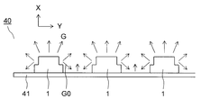
- the front view which shows the light-emitting device module which mounts the light-emitting device of 1st Embodiment of this invention.
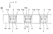
- the top view which shows the light-emitting device module which mounts the light-emitting device of 1st Embodiment of this invention.
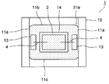
- the top view which shows the other aspect of the light-emitting device of 1st Embodiment of this invention.
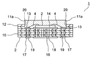
- Sectional drawing which shows the further another aspect of the light-emitting device of 1st Embodiment of this invention.
- the perspective view which shows the light-emitting device of 2nd Embodiment of this invention.
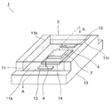
- FIG. 1 and 2 are perspective views showing the light emitting device of the first embodiment.
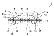
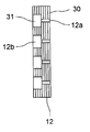
- FIG. 3 is a cross-sectional view taken along the line AA in FIG.
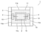
- the light emitting device 1 includes a base body 10 having a filling groove 11 provided in a concave shape on the upper surface.
- the filling groove 11 has side walls 11b and 11c that extend in one direction and are opposed to each other, and has open surfaces 11a that are opened on two opposed surfaces at both ends of the side walls 11b and 11c.
- the substrate 10 is formed by laminating ceramic sheets 12.
- the base 10 is provided with a heat radiating via 18 and an electrode via 19 extending downward from the bottom surface of the filling groove 11 and penetrating therethrough.
- a heat transfer portion 14 is formed on the upper surface of the heat dissipation via 18, and a heat dissipation portion 16 is formed on the lower surface.
- the light emitting element 2 made of LED is fixed on the heat transfer section 14 by adhesion or the like. This The light emitting element 2 is installed on the bottom surface of the filling groove 11. The heat generated by the light emitting element 2 is transmitted from the heat transfer section 14 to the heat dissipation section 16 through the heat dissipation via 18 to dissipate heat.
- a terminal 13 is formed on the upper surface of the electrode via 19 and an electrode 17 is formed on the lower surface.
- the terminal 13 and the electrode 17 are electrically connected by the electrode via 19.
- the light emitting element 2 is connected to the terminal 13 by a wire 4.
- the filling groove 11 is filled with a sealing material 3 made of a transparent resin containing dispersed phosphor particles.
- the light emitting element 2 is sealed by the sealing material 3.
- the light emitted from the light emitting element 2 is guided through the sealing material 3 and is converted in wavelength when it reaches the phosphor. Then, the wavelength-converted light and the light that does not reach the phosphor are mixed and emitted from the upper surface of the filling groove 11 and emitted from the open surface 11a facing the side surface. Thereby, the directivity angle of the emitted light of the light emitting device 1 is small in the direction in which the side walls 11b and 11c of the filling groove 11 face each other, and increases in the direction in which the open surface 11a faces.
- the manufacturing process of the light emitting device 1 includes a base material forming process, an element installation process, a sealing material filling process, a sealing material cutting process, and a slicing process.
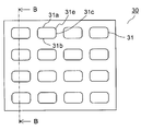
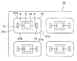
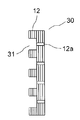
- FIG. 4 is a plan view showing the base material 30 formed in the base material forming step.
- FIG. 5 is a cross-sectional view taken along the line BB in FIG.
- a plurality of ceramic sheets 12 having a thickness of about 0.1 mm are laminated. Thereby, the base material 30 is formed.
- Each lower ceramic sheet 12 is provided with a hole 12a.
- the heat radiation via 18 and the electrode via 19 are formed by the hole 12a.
- the heat radiating via 18 and the electrode via 19 are filled with a conductive material.
- Each upper ceramic sheet 12 is provided with a hole 12b.
- a plurality of recesses 31 are formed in the matrix by being recessed in the upper surface of the base material 30 by the holes 12b.
- the concave portion 31 is formed in a substantially rectangular shape in plan view having an annular inner peripheral wall, and curved surface portions 31e are provided at four corners.
- the recessed part 31 has the 1st, 2nd side wall 31a, 31b which the both ends are mutually non-parallel, and it connects with the connection part 31c which the both ends of the 1st side wall 31a and the 2nd side wall 31b mutually opposed. Is done.
- the base material 30 is obtained by firing and integrating at about 1000 ° C. in a firing furnace.
- the terminal 13, the electrode 17, the heat transfer part 14, and the heat dissipation part 16 may be formed by firing simultaneously with the ceramic sheet 12, or may be formed after firing. Thereafter, the terminal 13, the electrode 17, the heat transfer unit 14, and the heat dissipation unit 16 are plated.
- FIG. 6 is a plan view showing an element installation process.
- the light emitting element 2 is bonded onto the heat transfer section 14 with a resin having a good thermal conductivity or a metal material having a good thermal conductivity.
- the light emitting element 2 is disposed on the bottom surface of the recess 31.
- the terminal part (not shown) of the light emitting element 2 and the terminal 13 are connected by the wire 4.
- FIG. 7 is a plan view showing a sealing material filling step.
- the sealing material 3 is filled into the recess 31.
- the light emitting element 2 is sealed by curing the sealing material 3.
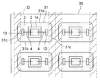
- FIG. 8 is a plan view showing a sealing material cutting step.
- the sealing material cutting step the sealing material 3 is cut across the first and second side walls 31a and 31b of the recess 31 by dicing using a rotating grindstone or the like.
- D indicates the cutting position of the rotating grindstone.
- the cutting depth of the rotating grindstone is the same as that of the concave portion 31, and the sealing material 3 is cut by grooving with the rotating grindstone.
- the first and second side walls 31a and 31b of the recess 31 are simultaneously cut, and the connecting portion 31c of the recess 31 is removed.
- the sealing material 3 is exposed laterally at both ends of the first and second side walls 31a and 31b, and an open surface 11a (see FIG. 1) of the filling groove 11 is formed.
- the side walls 11b and 11c (see FIG. 1) of the filling groove 11 are formed by the first and second side walls 31a and 31b.
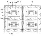
- FIG. 9 is a plan view showing a slicing step.
- the substrate material 30 is fully cut at a predetermined position around the recess 31 by dicing using a rotating grindstone or the like.
- E and F indicate cutting positions of the rotating grindstone.
- a plurality of bases 10 (refer to Drawing 1) are cut out from base material 30, and light-emitting device 1 is obtained.
- FIGS. 10 and 11 are a front view and a top view showing a light emitting device module 40 in which a plurality of the above light emitting devices 1 are arranged side by side.
- the light emitting device module 40 is used in the backlight 50 shown in FIG.
- the light emitting device 1 is mounted on a substrate 41 extending in one direction, and a plurality of light emitting devices 1 are arranged in parallel in one direction. Moreover, the open surface 11a of the adjacent light-emitting device 1 is opposingly arranged.
- the substrate 41 exposes a resin or metal main material having a high surface reflectance.
- the emitted light of the light emitting device 1 is emitted from the upper surface and the open surface 11a as indicated by an arrow G. Since the directivity angle of the emitted light is large in the direction in which the open surface 11a faces (Y direction), the interval between the light emitting devices 1 can be increased. Further, since the directivity angle of the emitted light of the light emitting device 1 is small in the direction in which the side walls 11b and 11c of the filling groove 11 face each other, the light traveling on the outside of the incident surface 51b (see FIG. 18) of the light guide plate 51 and the incident surface 51b The light reflected by can be reduced. Therefore, the cost of the light emitting device module 40 can be reduced and the light use efficiency can be improved.
- FIG. 12 is a plan view showing the light emitting device 1 formed thereby. Since the first side wall 31a and the second side wall 31b are formed non-parallel at both ends by the curved surface portion 31e, the opening area of the open surface 11a can be varied depending on the cutting position. Thereby, the light quantity of the emitted light from the open surface 11a can be adjusted with a cutting position.
- FIG. 13 is a cross-sectional view showing the light emitting device 1 formed thereby, and shows the same cross section as that of FIG. Since the cutting depth for cutting the sealing material 3 is shallower than the depth of the recess 31, a stepped portion 20 lower than the lower end of the open surface 11 a is formed at the bottom of the filling groove 11.
- a part of the light emitted from the light emitting element 2 arranged in the stepped portion 20 is blocked by the wall surface of the stepped portion 20, and the amount of light emitted from the open surface 11a and the directivity angle in the direction in which the open surface 11a faces are suppressed. Is done. Thereby, the directivity angle can be adjusted by changing the cutting depth. Further, since the sealing material 3 is in contact with the wall surface of the stepped portion 20, the contact area with the base 10 is increased, and the adhesion strength of the sealing material 3 can be improved.
- the filling groove 11 that is recessed in the base 10 and filled with the sealing material 3 has the open surfaces 11a on the two surfaces facing in one direction.
- the light is guided and emitted from the upper surface and the open surface 11a.
- the directivity angle of the emitted light of the light emitting device 1 can be reduced in the direction in which the side walls 11b and 11c of the filling groove 11 face each other, and can be increased in the direction in which the open surface 11a faces.
- the interval between the light emitting devices 1 can be increased in a device such as the light emitting device module 40 in which a plurality of light emitting devices 1 are arranged in one direction, thereby reducing the cost of the device equipped with the light emitting device 1 and using light. Efficiency can be improved.
- the step part 20 lower than the lower end of the open surface 11a is formed on the bottom surface of the filling groove 11 and the light emitting element 2 is arranged in the step part 20, the contact area between the sealing material 3 and the substrate 10 increases. The adhesion strength of the sealing material 3 can be improved.
- the two opposing surfaces of the sealing material 3 are cut together with the first side wall 31a and the second side wall 31b so as to intersect the first side wall 31a and the second side wall 31b facing each other of the recess 31 provided in the base material 30. Since the sealing material cutting step is provided, it is possible to easily realize the filling groove 11 having the open surfaces 11a on the two surfaces that are filled with the sealing material 3 and face in one direction.
- the stepped portion 20 can be easily formed at the bottom of the filling groove 11. Thereby, the light quantity and directivity angle of the emitted light from the open surface 11a can be adjusted easily.
- the opening area of the open surface 11a can be varied depending on the cutting position. Thereby, the light quantity of the emitted light from the open surface 11a can be adjusted with a cutting position.
- FIG. 14 shows a perspective view of the light emitting device 1 of the second embodiment.
- the base material 30 is fully cut in the sealing material cutting step to cut out the base 10. Thereby, it can serve as a sealing material cutting process and a slicing process. Accordingly, the number of manufacturing steps for the light emitting device 1 can be reduced.
- the stepped portion 20 shown in FIG. 13 can be formed by narrowing the opening area of the holes 12b (see FIG. 5) of some ceramic sheets 12. Thereby, the depth of the stepped portion 20 is determined when the base material 30 is formed in the base material forming process.
- the depth of the stepped portion 20 is changed by changing the cutting depth of the sealing material cutting step after the sealing agent 3 is filled. Can be varied. Therefore, when the light-emitting device 1 in which the depth of the stepped portion 20 is different for a plurality of models is required, the work-in-process can be made common if the sealing material cutting step and the slicing step are separated.
- the recess 31 provided in the base material 30 has a first side wall 31a and a second side wall 31b formed in a substantially rectangular shape in a plan view, but the first side wall 31a and the second side wall facing each other.
- the side wall 31b may be formed by a curved surface.
- the 1st side wall 31a and the 2nd side wall 31b can be formed non-parallel in the cutting position vicinity of a sealing material cutting process.
- the connecting portion 31c that connects the first side wall 31a and the second side wall 31b is formed in an oval shape or a circle that is integral with the first side wall 31a and the second side wall 31b in plan view. May be.
- the recess 31 of the base material 30 may be formed in a groove shape extending in one direction as shown in FIGS. 16 shows a plan view of the base material 30, and FIG. 17 shows a cross-sectional view taken along the line CC of FIG.
- a light-emitting device 1 similar to that shown in FIGS. 1 and 14 can be obtained according to the cutting depth in the sealing material cutting step.
- the first side wall 31a and the second side wall 31b opposed to the recess 31 may be viewed in a plan view to have a wave shape.
- the 1st side wall 31a and the 2nd side wall 31b can be formed non-parallel in the cutting position vicinity of a sealing material cutting process.
- the present invention can be used for an edge light type backlight mounted with a light emitting device module in which light emitting elements are arranged in one direction, a light source for a scanner, LED illumination, and the like.
Landscapes
- Led Device Packages (AREA)
Abstract
【課題】発光装置を搭載した機器のコストを削減するとともに光の利用効率を向上できる発光装置を提供する。 【解決手段】一方向に対向する二面に開放面11aを有した充填溝11が凹設される基体10と、充填溝11の底面に設置される発光素子2と、充填溝11に充填して発光素子2を封止する透明樹脂から成る封止材3とを備えた。
Description
本発明は、基体内に発光素子を封止した発光装置及びその製造方法に関する。また本発明は、基体内に発光素子を封止した発光装置を一方向に並設した発光装置モジュールに関する。
従来の発光装置は特許文献1に開示されている。この発光装置は上部に有底の円錐台形状の充填孔を凹設した基体を備え、充填孔の底面にLED等の発光素子が設置される。充填孔内には透明樹脂から成る封止材が充填され、発光素子が封止される。
発光素子の発光は封止材の内部を上方及び側方に導光し、側方に進行した光は傾斜面から成る充填孔の内周壁で反射して上方に進行する。これにより、充填孔の上面から充填孔の内周壁の傾斜角度に応じた所定の指向角で光が出射される。
また、特許文献2には充填孔よりも上方に封止材を突出させた発光装置が開示されている。発光素子の発光は封止材の内部を導光し、充填孔よりも上方の封止材の上面及び周面から出射される。これにより、発光装置の出射光の指向角を広くすることができる。
図18は液晶表示装置等に用いられるエッジライト型のバックライトを示す斜視図である。バックライト50は複数の発光装置1を有する発光装置モジュール40と、導光板51とを備えている。発光装置モジュール40は基板41上に複数の発光装置1を実装し、発光装置1が直線状に一方向に並設される。平板状の導光板51は表示パネル(不図示)に対向して出射面51aが配置される。導光板51の一側面から成る入射面51bに対向して発光装置モジュール40が配置され、発光装置1の上面が入射面51bに対向する。
発光装置1は入射面51bの方向(X方向)に光を出射する。入射面51bから導光板51に入射した光は導光板51内を導光して出射面51aから出射される。これにより、表示パネルが照明される。
上記特許文献1に開示された発光装置によると、各発光装置1は充填孔の内周壁の傾斜によって発光装置1の並設方向(Y方向)及び並設方向に垂直な方向(Z方向)に所定の指向角を有する。このため、発光装置1の間隔が大きくなると、発光装置1間の領域に光量が不足して暗部が形成され、輝度ムラが発生する。従って、暗部が形成されないように発光装置1の間隔を小さくする必要があるため、発光装置1を多く必要として発光装置モジュール40のコストがかかる問題があった。
上記特許文献2に開示された発光装置によると、Y方向の指向角が広くなるため、発光装置1の間隔を大きくすることができる。従って、発光装置モジュール40のコストを削減することができる。しかしながら、Z方向の指向角も広くなるため、入射面51aの外側に進行する光や入射面51aで反射する光が増加する。従って、発光装置1の出射光の利用効率が低下する問題があった。
本発明は、発光装置を搭載した機器のコストを削減するとともに光の利用効率を向上できる発光装置及びその製造方法を提供することを目的とする。また本発明は、コストを削減するとともに光の利用効率を向上できる発光装置モジュールを提供することを目的とする。
上記目的を達成するために本発明の発光装置は、一方向に対向する二面に開放面を有した充填溝が凹設される基体と、前記充填溝の底面に設置される発光素子と、前記充填溝に充填して前記発光素子を封止する透明樹脂から成る封止材とを備えたことを特徴としている。
この構成によると、基体に凹設された充填溝の底面に発光素子が配され、充填溝内に封止材を充填して発光素子が封止される。充填溝は一方向に対向する二面に開放面が形成され、発光素子の発光は封止材を導光して充填溝の上面から出射されるとともに側面に対向する開放面から出射される。これにより、発光装置の出射光の指向角は充填溝の側壁が対向する方向に小さく、開放面が対向する方向に大きくなる。
また本発明は、上記構成の発光装置において、前記基体がセラミックにより形成されることを特徴としている。
また本発明は、上記構成の発光装置において、前記充填溝の底面に前記開放面の下端よりも低い段部を形成し、前記発光素子を前記段部内に配したことを特徴としている。この構成によると、発光素子で発光した光の一部が段部の壁面によって遮られ、開放面からの出射光の光量及び開放面が対向する方向の指向角が抑制される。また、封止材が段部の壁面と接するため基体との接触面積が増加し、封止材の付着強度が向上する。
また本発明は、上記構成の発光装置において、前記充填溝の対向する側壁が両端部で非平行に形成されることを特徴としている。
また本発明の発光装置モジュールは、上記構成の発光装置を複数並設し、隣接する前記発光装置の前記開放面が対向配置されることを特徴としている。
また本発明の発光装置の製造方法は、基体素材に凹設された凹部の底面に発光素子を設置する素子設置工程と、前記凹部内に透明樹脂から成る封止材を充填して前記発光素子を封止する封止材充填工程と、前記凹部の対向する第1側壁及び第2側壁に交差して前記封止材の対向する二面を第1側壁及び第2側壁とともに切断する封止材切断工程とを備えたことを特徴としている。
この構成によると、環状の内壁または対向する二面が開放された内壁を有する凹部が基体素材に凹設され、素子設置工程で凹部の底面に発光素子が接着等により設置される。封止材充填工程では凹部内に封止材が充填され、発光素子が封止される。封止材切断工程では凹部の対向する第1側壁及び第2側壁に交差して封止材の対向する二面がダイシング加工等によって切断される。これにより、封止材を充填した凹部の対向する二面が切断され、封止材の切断面で開放される開放面を有した充填溝が形成される。
また本発明は、上記構成の発光装置の製造方法において、前記凹部が第1側壁と第2側壁とを連結部で連結した環状の内周壁を有し、前記封止材切断工程で前記連結部を除去したことを特徴としている。この構成によると、基体素材には環状の内壁を有する凹部が凹設される。封止材切断工程で封止材は対向する第1側壁及び第2側壁に交差して切断され、第1側壁と第2側壁とを連結する連結部が除去される。
また本発明は、上記構成の発光装置の製造方法において、前記封止材切断工程の切り込み深さが前記凹部の深さよりも浅いことを特徴としている。この構成によると、封止材切断工程で凹部の下部を残して封止材が切断され、切断面によって封止材を充填する充填溝の開放面が形成される。これにより、開放面の下端よりも低い段部が充填溝の底面に形成される。
また本発明は、上記構成の発光装置の製造方法において、第1側壁及び第2側壁が前記封止材切断工程の切断位置近傍で非平行に形成されることを特徴としている。この構成によると、封止材切断工程の切断位置によって開放面の開口面積が可変される。従って、開放面の出射光の光量を切断位置によって調整することができる。
本発明の発光装置によると、基体に凹設して封止材を充填した充填溝が一方向に対向する二面に開放面を有するので、発光素子の発光は封止材を導光して上面及び開放面から出射される。これにより、発光装置の出射光の指向角を充填溝の側壁が対向する方向に小さく、開放面が対向する方向に大きくすることができる。従って、複数の発光装置を一方向に並設した機器において発光装置の間隔を大きくすることができ、発光装置を搭載した機器のコストを削減するとともに光の利用効率を向上することができる。
また本発明の発光装置モジュールによると、基体に凹設して封止材を充填した充填溝が一方向に対向する二面に開放面を有する発光装置を複数並設し、隣接する発光装置の開放面が対向配置されるので、発光装置の間隔を大きくすることができる。従って、発光装置モジュールのコストを削減するとともに光の利用効率を向上することができる。
また本発明の発光装置の製造方法によると、凹部の対向する第1側壁及び第2側壁に交差して封止材の対向する二面を第1側壁及び第2側壁とともに切断する封止材切断工程を備えるので、封止材を充填して一方向に対向する二面に開放面を有する充填溝を容易に実現することができる。
以下に本発明の実施形態を図面を参照して説明する。図1、図2は第1実施形態の発光装置を示す斜視図である。また、図3は図1のA-A断面図を示している。発光装置1は上面に充填溝11を凹設した基体10を備えている。充填溝11は一方向に延びて対向する側壁11b、11cを有し、側壁11b、11cの両端の対向する二面に開放された開放面11aを有している。
基体10はセラミックシート12を積層して形成される。基体10には充填溝11の底面から下方に延びて貫通する放熱ビア18及び電極ビア19が設けられる。放熱ビア18の上面には伝熱部14が形成され、下面には放熱部16が形成される。
伝熱部14上にはLEDから成る発光素子2が接着等により固着される。これにより、
発光素子2が充填溝11の底面に設置される。発光素子2の発熱は放熱ビア18を介して
伝熱部14から放熱部16に伝えられて放熱する。
発光素子2が充填溝11の底面に設置される。発光素子2の発熱は放熱ビア18を介して
伝熱部14から放熱部16に伝えられて放熱する。
電極ビア19の上面には端子13が形成され、下面には電極17が形成される。電極ビア19によって端子13と電極17とが導通する。発光素子2はワイヤー4によって端子13に接続される。
充填溝11内には蛍光体の粒子を分散して含有した透明樹脂から成る封止材3が充填される。封止材3によって発光素子2が封止される。
発光素子2の発光は封止材3を導光し、蛍光体に到達すると波長変換される。そして、波長変換された光と蛍光体に到達しない光とが混合して充填溝11の上面から出射されるとともに側面の対向する開放面11aから出射される。これにより、発光装置1の出射光の指向角は充填溝11の側壁11b、11cが対向する方向に小さく、開放面11aが対向する方向に大きくなる。
次に、発光装置1の製造方法を説明する。発光装置1の製造工程は基体素材形成工程、素子設置工程、封止材充填工程、封止材切断工程及びスライス工程を備えている。図4は基体素材形成工程で形成される基体素材30を示す平面図である。また、図5は図4のB-B断面図を示している。
基体素材形成工程では厚さが約0.1mmの複数のセラミックシート12を積層する。これにより、基体素材30が形成される。下部の各セラミックシート12には孔部12aが設けられる。孔部12aによって放熱ビア18及び電極ビア19(図3参照)が形成される。放熱ビア18及び電極ビア19には導電性材料が充填される。
上部の各セラミックシート12には孔部12bが設けられる。孔部12bによって基体素材30の上面に凹設してマトリクス状に配置される複数の凹部31が形成される。凹部31は環状の内周壁を有した平面視略矩形に形成され、四隅に曲面部31eが設けられる。これにより、凹部31は互いに対向して両端部が非平行な第1、第2側壁31a、31bを有し、第1側壁31aと第2側壁31bとの両端が互いに対向した連結部31cにより連結される。
セラミックシート12が積層されると焼成炉により約1000℃で焼成して一体化され、基体素材30が得られる。この時、端子13、電極17、伝熱部14及び放熱部16(いずれも図3参照)をセラミックシート12と同時に焼成して形成してもよく、焼成後に形成してもよい。その後、端子13、電極17、伝熱部14及び放熱部16にはメッキが施される。
次に、図6は素子設置工程を示す平面図である。素子設置工程では熱伝導性の良い樹脂または熱伝導性の良い金属材料等により伝熱部14上に発光素子2が接着される。これにより、凹部31の底面に発光素子2が配される。そして、ワイヤー4により発光素子2の端子部(不図示)と端子13とが接続される。
次に、図7は封止材充填工程を示す平面図である。封止材充填工程では凹部31内に封止材3が充填される。封止材3の硬化によって発光素子2が封止される。
次に、図8は封止材切断工程を示す平面図である。封止材切断工程では回転砥石を用いたダイシング加工等によって封止材3が凹部31の第1、第2側壁31a、31bに交差して切断される。図中、Dは回転砥石の切断位置を示している。回転砥石の切り込み深さは凹部31と同じ深さになっており、回転砥石により溝加工して封止材3が切断される。
この時、凹部31の第1、第2側壁31a、31bが同時に切断され、凹部31の連結部31cが除去される。これにより、第1、第2側壁31a、31bの両端で封止材3が側方に面して露出し、充填溝11の開放面11a(図1参照)が形成される。また、第1、第2側壁31a、31bにより充填溝11の側壁11b、11c(図1参照)が形成される。
次に、図9はスライス工程を示す平面図である。スライス工程では回転砥石を用いたダイシング加工等によって凹部31の周囲の所定位置で基体素材30がフルカットされる。図中、E、Fは回転砥石の切断位置を示している。これにより、基体素材30から複数の基体10(図1参照)が切り出され、発光装置1が得られる。
図10、図11は上記の発光装置1を複数並設した発光装置モジュール40を示す正面図及び上面図である。発光装置モジュール40は前述の図18に示すバックライト50等に用いられる。発光装置1は一方向に延びる基板41上に実装され、複数の発光装置1が直線状に一方向に並設される。また、隣接する発光装置1の開放面11aが対向配置される。基板41は表面の反射率を高くした樹脂または金属の主材を露出する。
発光装置1の出射光は矢印Gに示すように上面及び開放面11aから出射される。出射光の指向角は開放面11aが対向する方向(Y方向)に大きいため、発光装置1の間隔を大きくすることができる。また、発光装置1の出射光の指向角は充填溝11の側壁11b、11cが対向する方向に小さいため、導光板51の入射面51b(図18参照)の外側に進行する光や入射面51bで反射する光を減少させることができる。従って、発光装置モジュール40のコストを削減できるとともに光の利用効率を向上することができる。
また、基板41の反射率が高いため、開放面11aから出射して基板41に到達した光(矢印G0)は基板41で反射して入射面51bの方向(X方向)に進行する。従って、光の利用効率をより向上することができる。
尚、前述の図7に示す封止材切断工程で凹部31の曲面部31e上を切断してもよい。図12はこれにより形成した発光装置1を示す平面図である。曲面部31eによって第1側壁31a及び第2側壁31bが両端部で非平行に形成されるため、切断位置によって開放面11aの開口面積を可変することができる。これにより、開放面11aからの出射光の光量を切断位置によって調整することができる。
また、封止材切断工程の切り込み深さを凹部31の深さよりも浅くしてもよい。図13はこれにより形成した発光装置1を示す断面図であり、前述の図3と同じ断面を示している。凹部31の深さよりも封止材3を切断する切り込み深さが浅いため、充填溝11の底部には開放面11aの下端よりも低い段部20が形成される。
段部20内に配される発光素子2で発光した光の一部は段部20の壁面によって遮られ、開放面11aからの出射光の光量及び開放面11aが対向する方向の指向角が抑制される。これにより、切り込み深さを可変することによって指向角を調整することができる。また、封止材3が段部20の壁面と接するため基体10との接触面積が増加し、封止材3の付着強度を向上することができる。
本実施形態によると、基体10に凹設して封止材3を充填した充填溝11が一方向に対向する二面に開放面11aを有するので、発光素子2の発光は封止材3を導光して上面及び開放面11aから出射される。これにより、発光装置1の出射光の指向角を充填溝11の側壁11b、11cが対向する方向に小さく、開放面11aが対向する方向に大きくすることができる。従って、複数の発光装置1を一方向に並設した発光装置モジュール40等の機器において発光装置1の間隔を大きくすることができ、発光装置1を搭載した機器のコストを削減するとともに光の利用効率を向上することができる。
また、充填溝11の底面に開放面11aの下端よりも低い段部20を形成して発光素子2を段部20内に配したので、封止材3と基体10との接触面積が増加し、封止材3の付着強度を向上することができる。
また、基材素材30に凹設した凹部31の対向する第1側壁31a及び第2側壁31bに交差して封止材3の対向する二面を第1側壁31a及び第2側壁31bとともに切断する封止材切断工程を備えるので、封止材3を充填して一方向に対向する二面に開放面11aを有する充填溝11を容易に実現することができる。
また、封止材切断工程の切り込み深さが凹部31の深さよりも浅いので、充填溝11の底部に容易に段部20を形成することができる。これにより、開放面11aからの出射光の光量及び指向角を容易に調整することができる。
また、凹部31の第1側壁31a及び第2側壁31bが封止材切断工程の切断位置近傍で非平行に形成されるので、切断位置によって開放面11aの開口面積を可変することができる。これにより、開放面11aからの出射光の光量を切断位置によって調整することができる。
次に、図14は第2実施形態の発光装置1の斜視図を示している。説明の便宜上、前述の図1~図9に示す第1実施形態と同様の部分には同一の符号を付している。本実施形態は、封止材切断工程で基体素材30をフルカットして基体10を切り出している。これにより、封止材切断工程とスライス工程とを兼ねることができる。従って、発光装置1の製造工数を削減することができる。
この時、前述の図13に示す段部20は一部のセラミックシート12の孔部12b(図5参照)の開口面積を狭くすることにより形成することができる。これにより、段部20の深さは基体素材30を基体素材形成工程で形成した際に決められる。
第1実施形態に示すように封止材切断工程とスライス工程とを別工程で行うと、封止剤3の充填後に封止材切断工程の切り込み深さを可変して段部20の深さを可変することができる。従って、複数の機種に対して段部20の深さが異なる発光装置1を必要とする場合は、封止材切断工程とスライス工程とを別工程にすると仕掛品を共通化することができる。
第1、第2実施形態において、基体素材30に設けた凹部31は第1側壁31a及び第2側壁31bが略平面の平面視略矩形に形成されるが、対向する第1側壁31a及び第2側壁31bを曲面により形成してもよい。これにより、第1側壁31a及び第2側壁31bを封止材切断工程の切断位置近傍で非平行に形成することができる。この時、図15に示すように、第1側壁31a及び第2側壁31bを連結する連結部31cを平面的に見て第1側壁31a及び第2側壁31bと一体の楕円形や円形に形成してもよい。
また、基材素材30の凹部31を図16、図17に示すように一方向に延びる溝形状に形成してもよい。図16は基材素材30の平面図を示し、図17は図16のC-C断面図を示している。封止材切断工程の切断深さに応じて前述の図1、図14と同様の発光装置1を得ることができる。
この時、凹部31の対向する第1側壁31a及び第2側壁31bを平面的に見て波形状にしてもよい。これにより、第1側壁31a及び第2側壁31bを封止材切断工程の切断位置近傍で非平行に形成することができる。
本発明によると、発光素子を一方向に並設した発光装置モジュールを搭載するエッジライト型バックライト、スキャナ用光源、LED照明等に利用することができる。
1 発光装置
2 発光素子
3 封止材
4 ワイヤー
10 基体
11 充填溝
11a 開放面
11b、11c 側壁
12 セラミックシート
12a 孔部
13 端子
14 伝熱部
16 放熱部
17 電極
18 放熱ビア
19 電極ビア
20 段部
30 基体素材
31 凹部
31a 第1側壁
31b 第2側壁
31c 連結部
32 溝部
40 発光装置モジュール
41 基板
2 発光素子
3 封止材
4 ワイヤー
10 基体
11 充填溝
11a 開放面
11b、11c 側壁
12 セラミックシート
12a 孔部
13 端子
14 伝熱部
16 放熱部
17 電極
18 放熱ビア
19 電極ビア
20 段部
30 基体素材
31 凹部
31a 第1側壁
31b 第2側壁
31c 連結部
32 溝部
40 発光装置モジュール
41 基板
Claims (9)
- 一方向に対向する二面に開放面を有した充填溝が凹設される基体と、前記充填溝の底面に設置される発光素子と、前記充填溝に充填して前記発光素子を封止する透明樹脂から成る封止材とを備えたことを特徴とする発光装置。
- 前記基体がセラミックにより形成されることを特徴とする請求項1に記載の発光装置。
- 前記充填溝の底面に前記開放面の下端よりも低い段部を形成し、前記発光素子を前記段部内に配したことを特徴とする請求項1または請求項2に記載の発光装置。
- 前記充填溝の対向する側壁が両端部で非平行に形成されることを特徴とする請求項1に記載の発光装置。
- 請求項1に記載の発光装置を複数並設し、隣接する前記発光装置の前記開放面が対向配置されることを特徴とする発光装置モジュール。
- 基体素材に凹設された凹部の底面に発光素子を設置する素子設置工程と、前記凹部内に透明樹脂から成る封止材を充填して前記発光素子を封止する封止材充填工程と、前記凹部の対向する第1側壁及び第2側壁に交差して前記封止材の対向する二面を第1側壁及び第2側壁とともに切断する封止材切断工程とを備えたことを特徴とする発光装置の製造方法。
- 前記凹部が第1側壁と第2側壁とを連結部で連結した環状の内周壁を有し、前記封止材切断工程で前記連結部を除去したことを特徴とする請求項6に記載の発光装置の製造方法。
- 前記封止材切断工程の切り込み深さが前記凹部の深さよりも浅いことを特徴とする請求項7に記載の発光装置の製造方法。
- 第1側壁及び第2側壁が前記封止材切断工程の切断位置近傍で非平行に形成されることを特徴とする請求項6~請求項8のいずれかに記載の発光装置の製造方法。
Applications Claiming Priority (2)
| Application Number | Priority Date | Filing Date | Title |
|---|---|---|---|
| JP2010074839A JP2013127994A (ja) | 2010-03-29 | 2010-03-29 | 発光装置、発光装置モジュール及び発光装置の製造方法 |
| JP2010-074839 | 2010-03-29 |
Publications (1)
| Publication Number | Publication Date |
|---|---|
| WO2011122531A1 true WO2011122531A1 (ja) | 2011-10-06 |
Family
ID=44712227
Family Applications (1)
| Application Number | Title | Priority Date | Filing Date |
|---|---|---|---|
| PCT/JP2011/057555 Ceased WO2011122531A1 (ja) | 2010-03-29 | 2011-03-28 | 発光装置、発光装置モジュール及び発光装置の製造方法 |
Country Status (2)
| Country | Link |
|---|---|
| JP (1) | JP2013127994A (ja) |
| WO (1) | WO2011122531A1 (ja) |
Cited By (5)
| Publication number | Priority date | Publication date | Assignee | Title |
|---|---|---|---|---|
| JP2017168819A (ja) * | 2016-01-28 | 2017-09-21 | マブン オプトロニックス カンパニー リミテッドMaven Optronics Co., Ltd. | 非対称放射パターンを有する発光素子およびその製造方法 |
| US10008648B2 (en) | 2015-10-08 | 2018-06-26 | Semicon Light Co., Ltd. | Semiconductor light emitting device |
| KR20190118977A (ko) * | 2018-04-11 | 2019-10-21 | 니치아 카가쿠 고교 가부시키가이샤 | 발광장치 |
| US10553768B2 (en) | 2018-04-11 | 2020-02-04 | Nichia Corporation | Light-emitting device |
| US11664479B2 (en) | 2020-12-17 | 2023-05-30 | Nichia Corporation | Light emitting device and planar light source |
Families Citing this family (5)
| Publication number | Priority date | Publication date | Assignee | Title |
|---|---|---|---|---|
| US9864372B2 (en) | 2015-03-12 | 2018-01-09 | Nightingale Intelligent Systems | Automated drone systems |
| US11038086B2 (en) | 2016-03-07 | 2021-06-15 | Semicon Light Co., Ltd. | Semiconductor light-emitting element and manufacturing method therefor |
| KR101824589B1 (ko) * | 2016-05-31 | 2018-03-15 | 주식회사 세미콘라이트 | 반도체 발광소자 구조물 |
| KR101768549B1 (ko) * | 2016-03-22 | 2017-08-17 | 우리이앤엘 주식회사 | 반도체 발광소자 및 이를 제조하는 방법 |
| JP2021034642A (ja) * | 2019-08-28 | 2021-03-01 | 浜松ホトニクス株式会社 | 光半導体装置及び光半導体装置の製造方法 |
Citations (6)
| Publication number | Priority date | Publication date | Assignee | Title |
|---|---|---|---|---|
| JP2004039778A (ja) * | 2002-07-02 | 2004-02-05 | Matsushita Electric Ind Co Ltd | 照明用発光素子 |
| JP2004127604A (ja) * | 2002-09-30 | 2004-04-22 | Citizen Electronics Co Ltd | 発光ダイオード及びバックライトユニット |
| JP2006216821A (ja) * | 2005-02-04 | 2006-08-17 | Citizen Electronics Co Ltd | 発光ダイオード |
| WO2008059650A1 (en) * | 2006-11-14 | 2008-05-22 | Harison Toshiba Lighting Corp. | Light emitting device, its manufacturing method and its mounted substrate |
| JP2008166462A (ja) * | 2006-12-28 | 2008-07-17 | Nichia Chem Ind Ltd | 発光装置 |
| JP2009038184A (ja) * | 2007-08-01 | 2009-02-19 | Harison Toshiba Lighting Corp | 半導体発光装置、光源装置及び面状発光装置 |
-
2010
- 2010-03-29 JP JP2010074839A patent/JP2013127994A/ja active Pending
-
2011
- 2011-03-28 WO PCT/JP2011/057555 patent/WO2011122531A1/ja not_active Ceased
Patent Citations (6)
| Publication number | Priority date | Publication date | Assignee | Title |
|---|---|---|---|---|
| JP2004039778A (ja) * | 2002-07-02 | 2004-02-05 | Matsushita Electric Ind Co Ltd | 照明用発光素子 |
| JP2004127604A (ja) * | 2002-09-30 | 2004-04-22 | Citizen Electronics Co Ltd | 発光ダイオード及びバックライトユニット |
| JP2006216821A (ja) * | 2005-02-04 | 2006-08-17 | Citizen Electronics Co Ltd | 発光ダイオード |
| WO2008059650A1 (en) * | 2006-11-14 | 2008-05-22 | Harison Toshiba Lighting Corp. | Light emitting device, its manufacturing method and its mounted substrate |
| JP2008166462A (ja) * | 2006-12-28 | 2008-07-17 | Nichia Chem Ind Ltd | 発光装置 |
| JP2009038184A (ja) * | 2007-08-01 | 2009-02-19 | Harison Toshiba Lighting Corp | 半導体発光装置、光源装置及び面状発光装置 |
Cited By (6)
| Publication number | Priority date | Publication date | Assignee | Title |
|---|---|---|---|---|
| US10008648B2 (en) | 2015-10-08 | 2018-06-26 | Semicon Light Co., Ltd. | Semiconductor light emitting device |
| JP2017168819A (ja) * | 2016-01-28 | 2017-09-21 | マブン オプトロニックス カンパニー リミテッドMaven Optronics Co., Ltd. | 非対称放射パターンを有する発光素子およびその製造方法 |
| KR20190118977A (ko) * | 2018-04-11 | 2019-10-21 | 니치아 카가쿠 고교 가부시키가이샤 | 발광장치 |
| US10553768B2 (en) | 2018-04-11 | 2020-02-04 | Nichia Corporation | Light-emitting device |
| KR102738697B1 (ko) | 2018-04-11 | 2024-12-06 | 니치아 카가쿠 고교 가부시키가이샤 | 발광장치 |
| US11664479B2 (en) | 2020-12-17 | 2023-05-30 | Nichia Corporation | Light emitting device and planar light source |
Also Published As
| Publication number | Publication date |
|---|---|
| JP2013127994A (ja) | 2013-06-27 |
Similar Documents
| Publication | Publication Date | Title |
|---|---|---|
| JP2013127994A (ja) | 発光装置、発光装置モジュール及び発光装置の製造方法 | |
| KR102215923B1 (ko) | 발광 모듈의 제조 방법 및 발광 모듈 | |
| US11187842B2 (en) | Light emitting module | |
| CN112310056B (zh) | 发光装置和面发光光源 | |
| JP5533830B2 (ja) | 線状光源装置 | |
| JP4144498B2 (ja) | 線状光源装置及びその製造方法、並びに、面発光装置 | |
| JP5545279B2 (ja) | 面状光源装置 | |
| JP2020087889A (ja) | 発光モジュール | |
| EP3511981B1 (en) | High light extraction efficiency, wavelength-converted devices | |
| JP7723290B2 (ja) | Ledパッケージ及び集積型発光装置 | |
| CN104576882A (zh) | 发光装置 | |
| TWI794592B (zh) | 發光模組 | |
| US20190355783A1 (en) | Led module | |
| WO2011122530A1 (ja) | 発光装置モジュール | |
| KR20170045698A (ko) | 발광 다이오드 패키지구조 | |
| CN114326204B (zh) | 发光模块以及面状光源 | |
| JP5507315B2 (ja) | 発光装置、バックライト光源およびその製造方法 | |
| WO2011122529A1 (ja) | 発光装置及び発光装置モジュール | |
| KR20140011080A (ko) | 디스플레이 장치 | |
| US20100238687A1 (en) | Semiconductor light emitting device | |
| JP2016167569A (ja) | 発光装置 | |
| JP5851262B2 (ja) | 線状光源装置、面発光装置、および液晶表示装置 | |
| US11506933B2 (en) | Light-emitting module, method for manufacturing the same, and liquid-crystal display device | |
| CN110364608B (zh) | 晶片级线型光源发光装置 | |
| JP2005167136A (ja) | 半導体発光装置及びその製造方法 |
Legal Events
| Date | Code | Title | Description |
|---|---|---|---|
| 121 | Ep: the epo has been informed by wipo that ep was designated in this application |
Ref document number: 11762755 Country of ref document: EP Kind code of ref document: A1 |
|
| NENP | Non-entry into the national phase |
Ref country code: DE |
|
| 122 | Ep: pct application non-entry in european phase |
Ref document number: 11762755 Country of ref document: EP Kind code of ref document: A1 |
|
| NENP | Non-entry into the national phase |
Ref country code: JP |