WO2011122497A1 - Transparent conductive film, method for producing same, and electronic device using transparent conductive film - Google Patents
Transparent conductive film, method for producing same, and electronic device using transparent conductive film Download PDFInfo
- Publication number
- WO2011122497A1 WO2011122497A1 PCT/JP2011/057459 JP2011057459W WO2011122497A1 WO 2011122497 A1 WO2011122497 A1 WO 2011122497A1 JP 2011057459 W JP2011057459 W JP 2011057459W WO 2011122497 A1 WO2011122497 A1 WO 2011122497A1
- Authority
- WO
- WIPO (PCT)
- Prior art keywords
- transparent conductive
- conductive film
- film
- gas barrier
- layer
- Prior art date
Links
Images


Classifications
-
- B—PERFORMING OPERATIONS; TRANSPORTING
- B32—LAYERED PRODUCTS
- B32B—LAYERED PRODUCTS, i.e. PRODUCTS BUILT-UP OF STRATA OF FLAT OR NON-FLAT, e.g. CELLULAR OR HONEYCOMB, FORM
- B32B9/00—Layered products comprising a layer of a particular substance not covered by groups B32B11/00 - B32B29/00
-
- C—CHEMISTRY; METALLURGY
- C23—COATING METALLIC MATERIAL; COATING MATERIAL WITH METALLIC MATERIAL; CHEMICAL SURFACE TREATMENT; DIFFUSION TREATMENT OF METALLIC MATERIAL; COATING BY VACUUM EVAPORATION, BY SPUTTERING, BY ION IMPLANTATION OR BY CHEMICAL VAPOUR DEPOSITION, IN GENERAL; INHIBITING CORROSION OF METALLIC MATERIAL OR INCRUSTATION IN GENERAL
- C23C—COATING METALLIC MATERIAL; COATING MATERIAL WITH METALLIC MATERIAL; SURFACE TREATMENT OF METALLIC MATERIAL BY DIFFUSION INTO THE SURFACE, BY CHEMICAL CONVERSION OR SUBSTITUTION; COATING BY VACUUM EVAPORATION, BY SPUTTERING, BY ION IMPLANTATION OR BY CHEMICAL VAPOUR DEPOSITION, IN GENERAL
- C23C14/00—Coating by vacuum evaporation, by sputtering or by ion implantation of the coating forming material
- C23C14/22—Coating by vacuum evaporation, by sputtering or by ion implantation of the coating forming material characterised by the process of coating
- C23C14/48—Ion implantation
-
- C—CHEMISTRY; METALLURGY
- C08—ORGANIC MACROMOLECULAR COMPOUNDS; THEIR PREPARATION OR CHEMICAL WORKING-UP; COMPOSITIONS BASED THEREON
- C08J—WORKING-UP; GENERAL PROCESSES OF COMPOUNDING; AFTER-TREATMENT NOT COVERED BY SUBCLASSES C08B, C08C, C08F, C08G or C08H
- C08J7/00—Chemical treatment or coating of shaped articles made of macromolecular substances
- C08J7/04—Coating
- C08J7/0427—Coating with only one layer of a composition containing a polymer binder
-
- C—CHEMISTRY; METALLURGY
- C08—ORGANIC MACROMOLECULAR COMPOUNDS; THEIR PREPARATION OR CHEMICAL WORKING-UP; COMPOSITIONS BASED THEREON
- C08J—WORKING-UP; GENERAL PROCESSES OF COMPOUNDING; AFTER-TREATMENT NOT COVERED BY SUBCLASSES C08B, C08C, C08F, C08G or C08H
- C08J7/00—Chemical treatment or coating of shaped articles made of macromolecular substances
- C08J7/04—Coating
- C08J7/043—Improving the adhesiveness of the coatings per se, e.g. forming primers
-
- C—CHEMISTRY; METALLURGY
- C08—ORGANIC MACROMOLECULAR COMPOUNDS; THEIR PREPARATION OR CHEMICAL WORKING-UP; COMPOSITIONS BASED THEREON
- C08J—WORKING-UP; GENERAL PROCESSES OF COMPOUNDING; AFTER-TREATMENT NOT COVERED BY SUBCLASSES C08B, C08C, C08F, C08G or C08H
- C08J7/00—Chemical treatment or coating of shaped articles made of macromolecular substances
- C08J7/04—Coating
- C08J7/044—Forming conductive coatings; Forming coatings having anti-static properties
-
- C—CHEMISTRY; METALLURGY
- C08—ORGANIC MACROMOLECULAR COMPOUNDS; THEIR PREPARATION OR CHEMICAL WORKING-UP; COMPOSITIONS BASED THEREON
- C08J—WORKING-UP; GENERAL PROCESSES OF COMPOUNDING; AFTER-TREATMENT NOT COVERED BY SUBCLASSES C08B, C08C, C08F, C08G or C08H
- C08J7/00—Chemical treatment or coating of shaped articles made of macromolecular substances
- C08J7/04—Coating
- C08J7/048—Forming gas barrier coatings
-
- C—CHEMISTRY; METALLURGY
- C08—ORGANIC MACROMOLECULAR COMPOUNDS; THEIR PREPARATION OR CHEMICAL WORKING-UP; COMPOSITIONS BASED THEREON
- C08J—WORKING-UP; GENERAL PROCESSES OF COMPOUNDING; AFTER-TREATMENT NOT COVERED BY SUBCLASSES C08B, C08C, C08F, C08G or C08H
- C08J7/00—Chemical treatment or coating of shaped articles made of macromolecular substances
- C08J7/12—Chemical modification
- C08J7/123—Treatment by wave energy or particle radiation
-
- C—CHEMISTRY; METALLURGY
- C23—COATING METALLIC MATERIAL; COATING MATERIAL WITH METALLIC MATERIAL; CHEMICAL SURFACE TREATMENT; DIFFUSION TREATMENT OF METALLIC MATERIAL; COATING BY VACUUM EVAPORATION, BY SPUTTERING, BY ION IMPLANTATION OR BY CHEMICAL VAPOUR DEPOSITION, IN GENERAL; INHIBITING CORROSION OF METALLIC MATERIAL OR INCRUSTATION IN GENERAL
- C23C—COATING METALLIC MATERIAL; COATING MATERIAL WITH METALLIC MATERIAL; SURFACE TREATMENT OF METALLIC MATERIAL BY DIFFUSION INTO THE SURFACE, BY CHEMICAL CONVERSION OR SUBSTITUTION; COATING BY VACUUM EVAPORATION, BY SPUTTERING, BY ION IMPLANTATION OR BY CHEMICAL VAPOUR DEPOSITION, IN GENERAL
- C23C14/00—Coating by vacuum evaporation, by sputtering or by ion implantation of the coating forming material
- C23C14/22—Coating by vacuum evaporation, by sputtering or by ion implantation of the coating forming material characterised by the process of coating
- C23C14/56—Apparatus specially adapted for continuous coating; Arrangements for maintaining the vacuum, e.g. vacuum locks
- C23C14/562—Apparatus specially adapted for continuous coating; Arrangements for maintaining the vacuum, e.g. vacuum locks for coating elongated substrates
-
- C—CHEMISTRY; METALLURGY
- C23—COATING METALLIC MATERIAL; COATING MATERIAL WITH METALLIC MATERIAL; CHEMICAL SURFACE TREATMENT; DIFFUSION TREATMENT OF METALLIC MATERIAL; COATING BY VACUUM EVAPORATION, BY SPUTTERING, BY ION IMPLANTATION OR BY CHEMICAL VAPOUR DEPOSITION, IN GENERAL; INHIBITING CORROSION OF METALLIC MATERIAL OR INCRUSTATION IN GENERAL
- C23C—COATING METALLIC MATERIAL; COATING MATERIAL WITH METALLIC MATERIAL; SURFACE TREATMENT OF METALLIC MATERIAL BY DIFFUSION INTO THE SURFACE, BY CHEMICAL CONVERSION OR SUBSTITUTION; COATING BY VACUUM EVAPORATION, BY SPUTTERING, BY ION IMPLANTATION OR BY CHEMICAL VAPOUR DEPOSITION, IN GENERAL
- C23C14/00—Coating by vacuum evaporation, by sputtering or by ion implantation of the coating forming material
- C23C14/58—After-treatment
-
- H—ELECTRICITY
- H01—ELECTRIC ELEMENTS
- H01B—CABLES; CONDUCTORS; INSULATORS; SELECTION OF MATERIALS FOR THEIR CONDUCTIVE, INSULATING OR DIELECTRIC PROPERTIES
- H01B5/00—Non-insulated conductors or conductive bodies characterised by their form
- H01B5/14—Non-insulated conductors or conductive bodies characterised by their form comprising conductive layers or films on insulating-supports
-
- C—CHEMISTRY; METALLURGY
- C08—ORGANIC MACROMOLECULAR COMPOUNDS; THEIR PREPARATION OR CHEMICAL WORKING-UP; COMPOSITIONS BASED THEREON
- C08J—WORKING-UP; GENERAL PROCESSES OF COMPOUNDING; AFTER-TREATMENT NOT COVERED BY SUBCLASSES C08B, C08C, C08F, C08G or C08H
- C08J2367/00—Characterised by the use of polyesters obtained by reactions forming a carboxylic ester link in the main chain; Derivatives of such polymers
- C08J2367/02—Polyesters derived from dicarboxylic acids and dihydroxy compounds
-
- C—CHEMISTRY; METALLURGY
- C08—ORGANIC MACROMOLECULAR COMPOUNDS; THEIR PREPARATION OR CHEMICAL WORKING-UP; COMPOSITIONS BASED THEREON
- C08J—WORKING-UP; GENERAL PROCESSES OF COMPOUNDING; AFTER-TREATMENT NOT COVERED BY SUBCLASSES C08B, C08C, C08F, C08G or C08H
- C08J2369/00—Characterised by the use of polycarbonates; Derivatives of polycarbonates
-
- C—CHEMISTRY; METALLURGY
- C08—ORGANIC MACROMOLECULAR COMPOUNDS; THEIR PREPARATION OR CHEMICAL WORKING-UP; COMPOSITIONS BASED THEREON
- C08J—WORKING-UP; GENERAL PROCESSES OF COMPOUNDING; AFTER-TREATMENT NOT COVERED BY SUBCLASSES C08B, C08C, C08F, C08G or C08H
- C08J2483/00—Characterised by the use of macromolecular compounds obtained by reactions forming in the main chain of the macromolecule a linkage containing silicon with or without sulfur, nitrogen, oxygen, or carbon only; Derivatives of such polymers
- C08J2483/14—Characterised by the use of macromolecular compounds obtained by reactions forming in the main chain of the macromolecule a linkage containing silicon with or without sulfur, nitrogen, oxygen, or carbon only; Derivatives of such polymers in which at least two but not all the silicon atoms are connected by linkages other than oxygen atoms
-
- Y—GENERAL TAGGING OF NEW TECHNOLOGICAL DEVELOPMENTS; GENERAL TAGGING OF CROSS-SECTIONAL TECHNOLOGIES SPANNING OVER SEVERAL SECTIONS OF THE IPC; TECHNICAL SUBJECTS COVERED BY FORMER USPC CROSS-REFERENCE ART COLLECTIONS [XRACs] AND DIGESTS
- Y10—TECHNICAL SUBJECTS COVERED BY FORMER USPC
- Y10T—TECHNICAL SUBJECTS COVERED BY FORMER US CLASSIFICATION
- Y10T428/00—Stock material or miscellaneous articles
- Y10T428/31504—Composite [nonstructural laminate]
- Y10T428/31652—Of asbestos
- Y10T428/31663—As siloxane, silicone or silane
Definitions
- the present invention relates to a transparent conductive film excellent in gas barrier properties and transparency, a method for producing the same, and an electronic device using the transparent conductive film.
- a polymer molded body such as a plastic film is inexpensive and excellent in processability, and thus has been used in various fields with a desired function.
- gas barrier plastic films that prevent the permeation of water vapor and oxygen are used in order to maintain the taste and freshness by suppressing the oxidation and alteration of proteins and fats and oils.
- a transparent plastic film is used instead of a glass plate as a substrate having electrodes in a display such as a liquid crystal display or an electroluminescence (EL) display in order to realize a reduction in thickness, weight, and flexibility. It is being considered.
- the plastic film has a problem that it easily transmits water vapor, oxygen, and the like as compared with a glass plate, and easily causes deterioration of elements inside the display.
- Patent Document 1 a flexible display substrate in which a transparent gas barrier layer made of a metal oxide is laminated on a transparent plastic film has been proposed.
- the flexible display substrate described in this document is obtained by laminating a transparent gas barrier layer made of a metal oxide on the surface of a transparent plastic film by vapor deposition, ion plating, sputtering, or the like.
- a transparent gas barrier layer made of a metal oxide
- ion plating ion plating
- sputtering or the like.
- this method has a problem in that sufficient gas barrier performance cannot be obtained unless the thickness of the gas barrier layer is in the micron order.
- the thickness of the gas barrier layer is 0.1 ⁇ m, it is described that the water vapor transmission rate is 0.50 g / m 2 / day.
- a transparent conductive film using a transparent plastic substrate uses ITO (tin-doped indium oxide) as a transparent conductive material. Since ITO uses indium, which is a rare metal, zinc oxide-based conductive materials have been proposed in recent years as ITO alternative transparent conductive materials. However, the zinc oxide-based conductive material has a problem of deterioration of sheet resistance value under wet heat conditions as compared with ITO.
- a transparent conductive material in which a zinc oxide film doped with silicon is provided on a hard coat layer provided on a plastic substrate has been proposed (see Patent Document 3).
- a transparent conductive material is a silicon oxide-doped zinc oxide film that reduces the temporal change of the sheet resistance value in a high temperature and high humidity environment, but the crystallinity is lowered and the conductivity is impaired. There is a problem.
- a transparent heating element has been proposed in which gallium oxide is added to the transparent conductive layer to improve heat resistance (see Patent Document 4).
- a transparent heating element must contain gallium oxide under predetermined conditions, and there is a problem that manufacturing conditions are limited.
- the water vapor barrier property is improved by providing an overcoat layer mainly composed of polyolefin on the transparent conductive layer (see Patent Document 6). Attempts have been made to control the sheet resistance in a high temperature environment by laminating a heat-resistant conductive layer on a gallium oxide-zinc oxide transparent conductive material.
- the sheet resistance value control under wet heat conditions is shown by increasing the doping amount of gallium oxide to a thickness of 400 nm (non-patent document). 1).
- the productivity itself is extremely inferior to the formation of the transparent conductive film at 400 nm, and the amount of gallium oxide to be doped is very large, which is not realistic from the viewpoint of the cost of raw materials.
- JP 2000-338901 A JP 2007-237588 A JP-A-8-45452 JP-A-6-187833 JP 2009-199812 A JP 2009-110897 A
- the present invention has been made in view of the above-described conventional technology, and has an excellent gas barrier property and transparent conductivity, and further has a low sheet resistance value even after a moist heat environment, and is excellent in conductivity.
- An object is to provide an electronic device using the manufacturing method and a transparent conductive film.
- the present inventors are composed of at least a material containing oxygen atoms and silicon atoms, and the surface layer portion has oxygen atoms, nitrogen atoms and silicon atoms present. It has been found that a film having a gas barrier layer having a specific value and having a film density of 2.4 to 4.0 g / cm 3 in the surface layer portion has excellent gas barrier properties. As a result, it was found that by laminating a zinc oxide-based conductive material, a transparent conductive film having a low sheet resistance value and excellent conductivity even after a wet heat environment was obtained, and the present invention was completed. Furthermore, it has been found that the gas barrier layer can be easily and efficiently manufactured by implanting ions into a layer containing a polysilazane compound, and the present invention has been completed.
- a gas barrier layer and a transparent conductive film are provided on at least one surface of a base material, and the gas barrier layer is made of a material containing at least oxygen atoms, nitrogen atoms, and silicon atoms.
- the oxygen atom existing ratio is 60 to 75%
- the nitrogen atom existing ratio is 0 to 10%
- the silicon atom existing is based on the total amount of oxygen atoms, nitrogen atoms and silicon atoms.
- the transparent conductive film is characterized in that the ratio is 25 to 35% and the film density in the surface layer portion of the gas barrier layer is 2.4 to 4.0 g / cm 3 .
- a second aspect of the present invention is the transparent conductive film according to the first aspect, wherein the gas barrier layer includes a polysilazane compound.
- a third aspect of the present invention is the transparent conductive film according to the first or second aspect, wherein the polysilazane compound is perhydropolysilazane.
- the gas barrier layer is a layer obtained by implanting ions into a layer containing a polysilazane compound. In the film.
- a fifth aspect of the present invention is characterized in that the ions are ionized at least one gas selected from the group consisting of hydrogen, nitrogen, oxygen, argon, helium, neon, xenon and krypton. It exists in the transparent conductive film as described in a 4th aspect.
- the gas barrier layer is a layer obtained by implanting ions into a layer containing a polysilazane compound by plasma ion implantation.
- the transparent conductive film is a layer obtained by implanting ions into a layer containing a polysilazane compound by plasma ion implantation.
- the gas barrier layer has a water vapor transmission rate of less than 0.50 g / m 2 / day in an atmosphere of 40 ° C. and 90% relative humidity. It exists in the transparent conductive film as described in the aspect.
- the eighth aspect of the present invention is the transparent conductive film according to any one of the first to seventh aspects, wherein the transparent conductive film is made of a metal oxide.
- the metal oxide is an indium oxide or a zinc oxide, and the main component is 90% by mass or more of indium oxide or zinc oxide, respectively. 8. It is in the transparent conductive film as described in any one of aspects.
- a step of implanting ions into a surface layer portion of a layer containing a polysilazane compound in a film having a layer containing a polysilazane compound on the surface and a step of forming a transparent conductive film thereon
- a transparent conductive film thereon
- An eleventh aspect of the present invention is characterized in that in the step of implanting ions, at least one gas selected from the group consisting of hydrogen, nitrogen, oxygen, argon, helium, neon, xenon and krypton is ion-implanted.
- at least one gas selected from the group consisting of hydrogen, nitrogen, oxygen, argon, helium, neon, xenon and krypton is ion-implanted.
- plasma ion implantation of at least one gas selected from the group consisting of hydrogen, nitrogen, oxygen, argon, helium, neon, xenon, and krypton is performed in the ion implantation step. It exists in the manufacturing method of the transparent conductive film as described in 10th aspect.
- the film is a long film having a layer containing a polysilazane compound on the surface, and ions are implanted into the layer containing the polysilazane compound while conveying the film in a certain direction.
- the method for producing a transparent conductive film according to any one of the tenth to twelfth aspects.
- an electronic device characterized by using the transparent conductive film described in any one of the first to ninth aspects.
- the transparent conductive film of the present invention can provide a transparent conductive film having excellent gas barrier performance, low sheet resistance even after wet heat environment, and excellent transparency and conductivity.
- the transparent conductive film of the present invention having excellent gas barrier properties can be produced safely and simply.
- the transparent conductive film of the present invention has a low sheet resistance even after a wet heat environment and has excellent gas barrier properties and transparent conductivity, it can be used to provide electronic devices such as displays and solar cells.
- the present invention will be described in detail by dividing it into 1) a transparent conductive film, 2) a method for producing a transparent conductive film, and 3) an electronic device.
- the transparent conductive film of the present invention comprises a gas barrier layer and a transparent conductive film on at least one side of a substrate, and the gas barrier layer contains at least oxygen atoms, nitrogen atoms and silicon atoms. It is composed of a material, and in the surface layer portion of the gas barrier layer, the oxygen atom existing ratio is 60 to 75% and the nitrogen atom existing ratio is 0 to 10% with respect to the total amount of oxygen atoms, nitrogen atoms and silicon atoms.
- the silicon atom content is 25 to 35%, and the film density in the surface layer portion of the gas barrier layer is 2.4 to 4.0 g / cm 3 .
- the transparent conductive film of the present invention has a gas barrier layer, (A) It is composed of a material containing at least an oxygen atom and a silicon atom, (B) In the surface layer portion, the proportion of oxygen atoms to the total amount of oxygen atoms, nitrogen atoms and silicon atoms is 60 to 75%, preferably 63.0 to 70.0%, and the proportion of nitrogen atoms is 0 to 10%, preferably 0.1 to 6.0%, the presence ratio of silicon atoms is 25 to 35%, preferably 29.0 to 32.0%, (C) The film density in the surface layer portion is 2.4 to 4.0 g / cm 3 .
- Examples of such a gas barrier layer include a layer obtained by implanting ions into a layer containing a polysilazane compound, as will be described later.
- the surface layer portion of the gas barrier layer refers to the surface of the gas barrier layer and a region from the surface to a depth of 5 nm.
- the surface of the gas barrier layer includes a boundary surface with another layer.
- the abundance ratio of oxygen atoms, nitrogen atoms and silicon atoms in the surface layer is measured by the method described in the examples.
- the film density can be calculated using an X-ray reflectivity method (XRR).
- XRR X-ray reflectivity method
- X-rays are totally reflected when they are incident on the thin film on the substrate at a very shallow angle.
- the angle of incident X-rays exceeds the total reflection critical angle, X-rays enter the thin film and are divided into transmitted waves and reflected waves at the thin film surface and interface, and the reflected waves interfere.
- the density of the film can be obtained. Note that the thickness of the thin film can also be obtained from measurement while changing the incident angle and analyzing the interference signal of the reflected wave accompanying the change in the optical path difference.
- the total reflection critical angle and film density can be measured and calculated using an X-ray reflectivity measuring apparatus.
- the film density can be measured by the following method, and in detail, it can be measured by the method described in Examples.
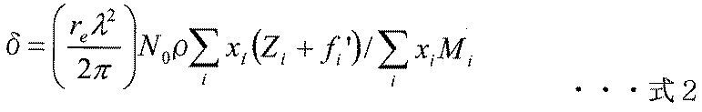
- the refractive index n of a substance with respect to X-rays and ⁇ of the real part of the refractive index n are expressed by the following formulas 1 and 2.
- re is the classical radius of the electron (2.818 ⁇ 10 ⁇ 15 m)
- N 0 is the Avogadro number
- ⁇ is the X-ray wavelength
- ⁇ is the density (g / cm 3 )
- Zi Mi Xi represents the atomic number
- fi ′ represents the atomic scattering factor (anomalous dispersion term) of the i-th atom.
- the total reflection critical angle ⁇ c is given by Equation 3 when ⁇ related to absorption is ignored.
- ⁇ c is a value that can be obtained from the X-ray reflectivity
- re, N 0 , and ⁇ are constants
- Zi, Mi, and fi ′ are values specific to the constituent atoms.
- xi atomic number ratio (molar ratio)
- the film density in the surface layer portion of the gas barrier layer is measured by the method described in Examples and is obtained using Equation 4.
- the transparent conductive film of the present invention is a layer obtained by implanting ions into a layer containing a polysilazane compound (hereinafter sometimes referred to as “polysilazane layer”) (hereinafter referred to as “ion implantation region”). There may be a thing having).
- a layer obtained by implanting ions into this polysilazane layer has a function as a gas barrier layer.
- the ion implantation region preferably satisfies the above requirements (a) to (c).
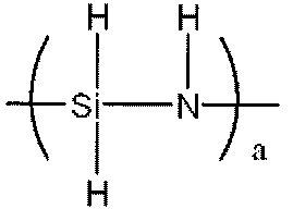
- polysilazane used in the present invention a compound having a repeating unit represented by the following formula (1) is preferable.
- the number average molecular weight of the polysilazane compound to be used is not particularly limited, but is preferably 100 to 50,000.
- n represents an arbitrary natural number.
- Rx, Ry, and Rz each independently represent a hydrogen atom, an unsubstituted or substituted alkyl group, an unsubstituted or substituted cycloalkyl group, an unsubstituted or substituted alkenyl group, unsubstituted or substituted Represents a non-hydrolyzable group such as an aryl group having a group or an alkylsilyl group;
- alkyl group of the unsubstituted or substituted alkyl group examples include a methyl group, an ethyl group, an n-propyl group, an isopropyl group, an n-butyl group, an isobutyl group, a sec-butyl group, a t-butyl group, Examples thereof include alkyl groups having 1 to 10 carbon atoms such as n-pentyl group, isopentyl group, neopentyl group, n-hexyl group, n-heptyl group and n-octyl group.
- Examples of the unsubstituted or substituted cycloalkyl group include cycloalkyl groups having 3 to 10 carbon atoms such as a cyclobutyl group, a cyclopentyl group, a cyclohexyl group, and a cycloheptyl group.
- alkenyl group of an unsubstituted or substituted alkenyl group examples include, for example, a vinyl group, 1-propenyl group, 2-propenyl group, 1-butenyl group, 2-butenyl group, 3-butenyl group and the like having 2 to 2 carbon atoms. 10 alkenyl groups are mentioned.
- substituents for the alkyl group, cycloalkyl group and alkenyl group include halogen atoms such as fluorine atom, chlorine atom, bromine atom and iodine atom; hydroxyl group; thiol group; epoxy group; glycidoxy group; (meth) acryloyloxy group
- halogen atoms such as fluorine atom, chlorine atom, bromine atom and iodine atom
- hydroxyl group such as hydroxyl group; thiol group; epoxy group; glycidoxy group; (meth) acryloyloxy group
- An unsubstituted or substituted aryl group such as a phenyl group, a 4-methylphenyl group, and a 4-chlorophenyl group;
- aryl group of an unsubstituted or substituted aryl group examples include aryl groups having 6 to 10 carbon atoms such as a phenyl group, a 1-naphthyl group, and a 2-naphthyl group.
- substituent of the aryl group examples include halogen atoms such as fluorine atom, chlorine atom, bromine atom and iodine atom; alkyl groups having 1 to 6 carbon atoms such as methyl group and ethyl group; carbon numbers such as methoxy group and ethoxy group 1-6 alkoxy groups; nitro groups; cyano groups; hydroxyl groups; thiol groups; epoxy groups; glycidoxy groups; (meth) acryloyloxy groups; unsubstituted phenyl groups, 4-methylphenyl groups, 4-chlorophenyl groups, etc.
- substituent of the aryl group examples include an aryl group having a substituent.
- alkylsilyl group examples include a trimethylsilyl group, a triethylsilyl group, a triisopropylsilyl group, a tri-t-butylsilyl group, a methyldiethylsilyl group, a dimethylsilyl group, a diethylsilyl group, a methylsilyl group, and an ethylsilyl group.
- Rx, Ry, and Rz a hydrogen atom, an alkyl group having 1 to 6 carbon atoms, or a phenyl group is preferable, and a hydrogen atom is particularly preferable.
- Examples of the polysilazane compound having a repeating unit represented by the formula (1) include inorganic polysilazanes in which Rx, Ry, and Rz are all hydrogen atoms, and organic polysilazanes in which at least one of Rx, Ry, and Rz is not a hydrogen atom. There may be.
- inorganic polysilazane the following
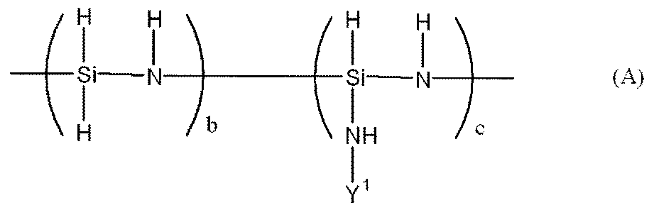
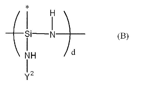
- Perhydropolysilazane having a linear structure having a repeating unit represented by formula (II), a molecular weight of 690 to 2000, and 3 to 10 SiH 3 groups in one molecule Japanese Patent Publication No. 63-16325)
- Examples thereof include perhydropolysilazane having a structure, a branched structure, and a cyclic structure.
- Examples of the organic polysilazane include the following (i) to (v).
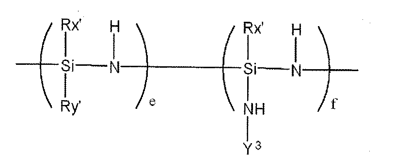
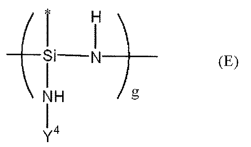
- Rx ′ is an unsubstituted or substituted alkyl group, an unsubstituted or substituted cycloalkyl group, an unsubstituted or substituted alkenyl group, unsubstituted or substituted An aryl group having a group, or an alkylsilyl group.
- Rx ′ is also the same), and having a cyclic structure having a degree of polymerization of 3 to 5, (Ii) — (Rx′SiHNRz ′) — (Rz ′) is an unsubstituted or substituted alkyl group, an unsubstituted or substituted cycloalkyl group, an unsubstituted or substituted alkenyl group, unsubstituted or An aryl group having a substituent or an alkylsilyl group) as a repeating unit, mainly having a cyclic structure with a degree of polymerization of 3 to 5, (Iii) — (Rx′Ry′SiNH) — (Ry ′ is an unsubstituted or substituted alkyl group, unsubstituted or substituted cycloalkyl group, unsubstituted or substituted alkenyl group, unsubstituted Or an aryl group having a substituent or an al
- the organic polysilazane can be produced by a conventionally known method. For example, it can be obtained by reacting ammonia or a primary amine with a reaction product of an unsubstituted or substituted halogenosilane compound represented by the following formula (2) and a secondary amine.
- the secondary amine, ammonia, and primary amine to be used may be appropriately selected according to the structure of the target polysilazane compound.
- a modified polysilazane compound can also be used as the polysilazane compound.
- the modified polysilazane include, for example, a polymetallosilazane containing a metal atom (the metal atom may be crosslinked) and repeating units of [(SiH 2 ) g (NH) h )] and [(SiH 2 ) i O] (wherein, g, h, i are each independently 1, 2 or 3.
- polysiloxazane JP 62-195024 discloses represented by)
- boron compound polysilazane Polyborosilazane produced by reacting polysilazane (Japanese Patent Laid-Open No.
- polymetallosilazane produced by reacting polysilazane and metal alkoxide Japanese Patent Laid-Open No. 63-81122, etc.
- inorganic silazane high polymer And modified polysilazanes JP-A-1-138108, etc.
- copolymerized silazanes obtained by introducing an organic component into polysilazane JP-A-2-175726, etc.
- Low temperature ceramicized polysilazanes Japanese Patent Laid-Open No.
- a polysilazane composition obtained by adding amines and / or acids Japanese Patent Laid-Open No. 9-31333
- a modified polysilazane obtained by adding alcohol such as methanol or hexamethyldisilazane to a terminal N atom to perhydropolysilazane JP-A -345826, JP Patent Laid-Open No. 4-63833 publication
- the polysilazane compound used in the present invention is preferably an inorganic polysilazane in which Rx, Ry, and Rz are all hydrogen atoms, and an organic polysilazane in which at least one of Rx, Ry, and Rz is not a hydrogen atom, From the viewpoint of forming an injection layer having excellent gas barrier properties, inorganic polysilazane is more preferable.
- the polysilazane compound a commercially available product as a glass coating material or the like can be used as it is.
- the layer containing a polysilazane compound may contain other components in addition to the polysilazane compound as long as the object of the present invention is not impaired.
- other components include curing agents, other polymers, anti-aging agents, light stabilizers, and flame retardants.
- the content of the polysilazane compound in the layer containing the polysilazane compound is preferably 50% by weight or more, more preferably 70% by weight or more from the viewpoint of forming an ion implantation region having excellent gas barrier properties. .
- the method for forming a layer containing a polysilazane compound is not particularly limited.
- a layer-forming solution containing at least one polysilazane compound, optionally other components, a solvent, and the like on a film-like substrate is used.
- coating on a suitable support body, and drying and forming the obtained coating film moderately is mentioned.
- the coating apparatus known apparatuses such as a spin coater, a knife coater, and a gravure coater can be used.
- Heating is performed at 80 to 150 ° C. for several tens of seconds to several tens of minutes.
- the layer containing the polysilazane compound is subjected to a plasma polymerization treatment by bringing a gas of a plasma polymerizable silazane compound such as dimethyldisilazane, tetramethyldisilazane, or hexamethyldisilazane into contact with a film-like substrate.
- a plasma polymerizable silazane compound such as dimethyldisilazane, tetramethyldisilazane, or hexamethyldisilazane
- the thickness of the layer containing the polysilazane compound to be formed is not particularly limited, but is usually 20 nm to 100 ⁇ m, preferably 30 to 500 nm, more preferably 40 to 200 nm. In the present invention, a transparent conductive film having sufficient gas barrier performance can be obtained even when the layer containing the polysilazane compound is nano-order.
- the gas barrier layer is preferably a layer containing at least one polysilazane compound, and more preferably has an ion-implanted region into which ions are implanted.
- the ion implantation amount may be appropriately determined according to the intended use (necessary gas barrier property, transparency, etc.) of the formed article to be formed.
- ions to be implanted include rare gases such as argon, helium, neon, krypton, and xenon, ions such as fluorocarbon, hydrogen, nitrogen, oxygen, carbon dioxide, chlorine, fluorine, sulfur, hydrocarbon, and silicon compounds; gold, silver And ions of conductive metals such as copper, platinum, nickel, palladium, chromium, titanium, molybdenum, niobium, tantalum, tungsten, and aluminum.
- rare gases such as argon, helium, neon, krypton, and xenon
- ions such as fluorocarbon, hydrogen, nitrogen, oxygen, carbon dioxide, chlorine, fluorine, sulfur, hydrocarbon, and silicon compounds
- gold, silver And ions of conductive metals such as copper, platinum, nickel, palladium, chromium, titanium, molybdenum, niobium, tantalum, tungsten, and aluminum.
- hydrogen, nitrogen, oxygen, argon, helium, neon, xenon, krypton, and silicon compounds can be implanted more easily and an ion implantation region having particularly excellent gas barrier properties and transparency can be obtained.
- at least one ion selected from the group consisting of hydrocarbons is preferred.
- the method for implanting ions is not particularly limited, and examples thereof include a method in which a layer containing a polysilazane compound is formed and then ions are implanted into the layer containing the polysilazane compound.
- Examples of the ion implantation method include a method of irradiating ions accelerated by an electric field (ion beam), a method of implanting ions in plasma, and the like. Among them, in the present invention, the latter method of implanting plasma ions is preferable because a gas barrier film can be easily obtained.
- plasma is generated in an atmosphere containing a plasma generation gas such as a rare gas, and a negative high voltage pulse is applied to a layer containing a polysilazane compound, whereby ions (positive ions) in the plasma are applied. Can be injected into the surface portion of the layer containing the polysilazane compound.
- a plasma generation gas such as a rare gas
- a negative high voltage pulse is applied to a layer containing a polysilazane compound, whereby ions (positive ions) in the plasma are applied.
- ions positive ions
- the thickness of the portion where the ion implantation region is formed can be controlled by the implantation conditions such as the type of ion, applied voltage, treatment time, etc., depending on the thickness of the layer containing the polysilazane compound, the intended use of the transparent conductive film, etc. Usually, it is 10 to 1000 nm.
- the ion implantation can be confirmed by performing an elemental analysis measurement at around 10 nm from the surface using X-ray photoelectron spectroscopy (XPS).
- XPS X-ray photoelectron spectroscopy
- the transparent conductive film of the present invention comprises a gas barrier layer and a transparent conductive film to be described later on at least one side of the substrate, but may further comprise other layers.
- the arrangement position of the other layers is not particularly limited, and the other layers may be a single layer or two or more of the same or different types.
- the base material which consists of materials other than a polysilazane compound is mentioned, for example.
- layers, such as a hard-coat layer can be provided for the purpose of shielding the oligomer component and low molecular component of the said base material, for example. It does not specifically limit as a hard-coat layer, The well-known thing which consists of energy-beam curable resin and thermosetting resin can be used.
- the thickness of the hard coat layer is preferably from 0.1 to 20 ⁇ m, particularly preferably from 1 to 10 ⁇ m.
- the substrate of the transparent conductive film of the present invention is not particularly limited as long as it meets the purpose of the transparent conductive film.
- polyimide, polyamide, polyamideimide, polyphenylene ether, polyetherketone, polyetheretherketone examples include polyolefin, polyester, polycarbonate, polysulfone, polyethersulfone, polyphenylsulfone, modified polysulfone, polyphenylene sulfide, polyarylate, acrylic resin, cycloolefin polymer, aromatic polymer, polyurethane polymer, and the like.
- fever and the radiation using the thermosetting type or radiation-curable resin are mentioned. These may also contain various additives such as antioxidants, flame retardants, high refractive materials, low refractive materials, and lubricants as long as they do not impair gas barrier properties, transparency, and conductivity.
- polyester, polyamide or cycloolefin polymer is preferable, and polyester or cycloolefin polymer is more preferable because of excellent transparency and versatility.
- polyester examples include polyethylene terephthalate, polybutylene terephthalate, polyethylene naphthalate, and polyarylate.
- polyamide examples include wholly aromatic polyamide, nylon 6, nylon 66, nylon copolymer, and the like.
- cycloolefin polymers include norbornene polymers, monocyclic olefin polymers, cyclic conjugated diene polymers, vinyl alicyclic hydrocarbon polymers, and hydrides thereof. Specific examples thereof include Apel (an ethylene-cycloolefin copolymer manufactured by Mitsui Chemicals), Arton (a norbornene polymer manufactured by JSR), Zeonoa (a norbornene polymer manufactured by Nippon Zeon), and the like. .
- the thickness of these base materials is preferably 0.01 to 0.5 mm, more preferably 0.05 to 0.25 mm. If it is these ranges, it is preferable at the point of transparency and bending resistance, and handling is easy.
- the arrangement position of the gas barrier layer is not particularly limited, but the transparent conductive film is directly on the ion implantation region for reasons such as efficient production. A structure that contacts is preferable.
- the gas barrier layer of the transparent conductive film of this invention may be formed only in the single side
- the transparent conductive film of the present invention is characterized in that a transparent conductive film is laminated on a gas barrier layer.
- the film can be provided with a function as an electrode and can be suitably used for an organic EL display element or the like.
- the composition of the transparent conductive film is not particularly limited.
- metals such as platinum, gold, silver, and copper, graphene, carbon materials such as carbon nanotubes, polyarinin, polyacetylene, polythiophene, polyparaphenylene vinylene, and polyethylenedioxythiophene
- Organic conductive materials such as tin oxide, indium oxide, cadmium oxide, tin-doped indium oxide (ITO), composite oxides such as tin and gallium-doped indium oxide (IGZO), chalcogenides, lanthanum hexaboride, titanium nitride, titanium carbide
- Non-oxidized compounds such as zinc oxide, zinc oxide and other oxides, zinc oxide doped indium oxide, fluorine doped indium oxide, antimony doped tin oxide, fluorine doped tin oxide, aluminum doped zinc oxide, gallium doped zinc oxide and other zinc oxide Conductive material And the like.
- the zinc oxide-based conductive material is mainly composed of zinc oxide, and preferably contains 90% by mass or more of zinc oxide, but the other composition is not particularly limited, for example, the resistivity is reduced. Therefore, various additives such as aluminum, indium, boron, gallium, silicon, tin, germanium, antimony, iridium, rhenium, cerium, zirconium, scandium, and yttrium may be added. These various additives may contain at least one kind, and the addition amount is preferably 0.05 to 10% by mass.
- the organic conductive material may contain iodine, arsenic pentafluoride, alkali metal, polyanion poly (styrene sulfonate), etc. as a dopant.
- Specific examples include polyethylene dioxythiophene (trade name “CLEVIOS P AI 4083” manufactured by Starck Vitec Co., Ltd.).
- the composition of the transparent conductive film is zinc-doped conductive material such as tin-doped indium oxide (ITO), zinc oxide, zinc oxide-doped indium oxide (IZO, registered trademark), or fluorine-containing tin oxide (FTO). It is preferable.
- ITO tin-doped indium oxide
- IZO zinc oxide-doped indium oxide
- FTO fluorine-containing tin oxide
- the transparent conductive film can be formed by a conventionally known method, for example, a sputtering method, an ion plating method, a vacuum deposition method, a chemical vapor deposition method, a coating method such as a bar coater or a micro gravure coater, etc. Can be formed.
- a film with gas barrier properties is preliminarily subjected to heat treatment in a temperature range not exceeding the melting point of the film under vacuum or atmospheric pressure, or a process of performing plasma treatment or ultraviolet irradiation treatment is provided. May be.
- the thickness of the transparent conductive film varies depending on the application, but is, for example, 10 nm to 5 ⁇ m, preferably 20 nm to 1000 nm, and more preferably 20 nm to 500 nm.
- the transparent conductive film of the present invention has excellent gas barrier properties, transparency and conductivity, and when the shape thereof is a film or sheet (hereinafter referred to as “film”), it has excellent bending resistance. Those which are excellent and maintain the gas barrier property even when they are bent are preferred.
- the transparent conductive film of the present invention has an excellent gas barrier property because the transparent conductive film of the present invention has a small gas permeability such as water vapor.
- the water vapor transmission rate is preferably less than 0.50 g / m 2 / day and more preferably 0.35 g / m 2 / day or less in an atmosphere of 40 ° C. and 90% relative humidity.
- steam, of a transparent conductive film can be measured using a well-known gas-permeability measuring apparatus.
- the sheet resistance value of the transparent conductive film of the present invention is preferably 1000 ⁇ / ⁇ or less, more preferably 500 ⁇ / ⁇ or less, and further preferably 100 ⁇ / ⁇ or less.
- the sheet resistance value of a transparent conductive film can be measured by a well-known method.
- the transparent conductive film of the present invention has an initial sheet resistance value of R 0, and sheet resistance values after being put into a 60 ° C. and 60 ° C. and 90% RH environment for 7 days, respectively, as R 1 and R 2 .
- T 1 is preferably 1.0 or less, more preferably 0.5 or less, and even more preferably 0.1 or less.
- T 2 is preferably 1.0 or less, and more preferably 0.2 or less.
- the visible light transmittance is a transmittance at a wavelength of 550 nm, preferably 70% or more, and more preferably 75% or more.
- the visible light transmittance of the transparent conductive film can be measured using a known visible light transmittance measuring device.
- the thickness of the transparent conductive film of the present invention is not particularly limited, but when used as an electronic device member, a thickness of about 1 to 1000 ⁇ m is preferable.
- the method for producing a transparent conductive film of the present invention includes a step of implanting ions into a surface layer portion of a layer containing a polysilazane compound in a film having a layer containing a polysilazane compound on the surface, and It has the process of forming a transparent conductive film on this ion implantation area
- a production method in which ions are implanted into a layer containing a polysilazane compound while a long film having a layer containing a polysilazane compound is conveyed in a certain direction is preferable.
- the film having a layer containing a polysilazane compound is a film in which a layer containing a polysilazane compound is formed on a substrate.
- a long film can be unwound from an unwinding roll, and ions can be injected while being conveyed in a certain direction, and can be wound up by a winding roll.
- the resulting film can be produced continuously.
- the long film having a layer containing a polysilazane compound may include only a layer containing a polysilazane compound or may include other layers.
- the same materials as those described above can be used.
- the thickness of the long film having a layer containing a polysilazane compound is preferably 1 ⁇ m to 500 ⁇ m, more preferably 5 ⁇ m to 300 ⁇ m, from the viewpoint of operability of unwinding, winding and conveying.
- the method for implanting ions into the layer containing the polysilazane compound is not particularly limited.
- a method of forming an ion implantation region in the surface layer portion of the layer by plasma ion implantation is particularly preferable.
- a negative high voltage pulse is applied to a layer surface exposed to a plasma and containing a polysilazane compound, so that ions in the plasma are implanted into the surface layer of the layer to form an ion implantation region. Is the method.
- (A) a method in which ions existing in plasma generated using an external electric field are implanted into the surface portion of the layer, or (B) the layer is formed without using an external electric field.
- a method of injecting ions present in the plasma generated only by the electric field by the negative high voltage pulse to be applied to the surface portion of the layer is preferable.
- the pressure during ion implantation is preferably 0.01 to 1 Pa.
- the pressure during plasma ion implantation is in such a range, a uniform ion implantation region can be easily and efficiently formed, and an ion implantation region having both transparency and gas barrier properties can be efficiently formed. Can do.
- the processing operation is simple, and the processing time can be greatly shortened. Further, the entire layer can be processed uniformly, and ions in the plasma can be continuously injected into the surface portion of the layer with high energy when a negative high voltage pulse is applied. Furthermore, without applying special other means such as radio frequency (hereinafter abbreviated as “RF”) or a high frequency power source such as a microwave, just applying a negative high voltage pulse to the layer, A high-quality ion-implanted region can be uniformly formed on the surface portion of the layer.
- RF radio frequency
- a high frequency power source such as a microwave
- the pulse width when applying a negative high voltage pulse is preferably 1 to 15 ⁇ sec.
- the pulse width is in such a range, a transparent and uniform ion implantation region can be formed more easily and efficiently.
- the applied voltage when generating plasma is preferably -1 kV to -50 kV, more preferably -1 kV to -30 kV, and particularly preferably -5 kV to -20 kV. If ion implantation is performed at an applied voltage greater than ⁇ 1 kV, the ion implantation amount (dose amount) becomes insufficient, and desired performance cannot be obtained. On the other hand, if ion implantation is performed at a value smaller than ⁇ 50 kV, the film is charged at the time of ion implantation, and problems such as coloring of the film occur, which is not preferable.
- Plasma ion-implanted ion species include: rare gases such as argon, helium, neon, krypton, and xenon, ions such as fluorocarbon, hydrogen, nitrogen, oxygen, carbon dioxide, chlorine, fluorine, sulfur, hydrocarbons, and silicon compounds; gold And ions of conductive metals such as silver, copper, platinum, nickel, palladium, chromium, titanium, molybdenum, niobium, tantalum, tungsten, and aluminum.
- rare gases such as argon, helium, neon, krypton, and xenon
- ions such as fluorocarbon, hydrogen, nitrogen, oxygen, carbon dioxide, chlorine, fluorine, sulfur, hydrocarbons, and silicon compounds
- gold And ions of conductive metals such as silver, copper, platinum, nickel, palladium, chromium, titanium, molybdenum, niobium, tantalum, tungsten, and aluminum.
- a plasma ion implantation apparatus is used when ions in plasma are implanted into the surface of the layer.
- high-frequency power is applied to a feedthrough that applies a negative high-voltage pulse to a layer containing an ( ⁇ ) polysilazane compound (hereinafter sometimes referred to as “ion-implanted layer”).
- ion-implanted layer a layer containing an ( ⁇ ) polysilazane compound
- An apparatus for attracting and injecting ions in plasma by applying a negative pulse while controlling the temperature by controlling the pulse constant and heating the layer to be ion-implanted 001-156003) ( ⁇ ) a plasma ion implantation apparatus for generating plasma using an external electric field such as a high-frequency power source such as a microwave, and attracting and injecting ions in the plasma by applying a high voltage pulse; ( ⁇ ) A plasma ion implantation apparatus for injecting ions in plasma generated only by an electric field generated by applying a high voltage pulse without using an external electric field.
- the plasma ion implantation apparatus ( ⁇ ) or ( ⁇ ) because the processing operation is simple, the processing time can be greatly shortened, and it is suitable for continuous use.
- FIG. 1 is a diagram showing an outline of a continuous plasma ion implantation apparatus including the plasma ion implantation apparatus ( ⁇ ).
- 1a is a long film having a layer containing a polysilazane compound (hereinafter referred to as "film"), 11a is a chamber, 20a is a turbo molecular pump, 3a is a film 1a before being ion-implanted.
- 5a is a winding roll for winding the ion-implanted film 1a into a roll shape
- 2a is a high voltage applied rotation can
- 6a is a film feeding roll
- 10a is a gas inlet
- 7a is a high voltage pulse
- a power source 4 is a plasma discharge electrode (external electric field).
- FIG. 1B is a perspective view of the high-voltage applying rotation can 2a, and 15 is a high-voltage introduction terminal (feedthrough).
- the long film 1a having a layer containing a polysilazane compound to be used on the surface is a film in which a layer containing a polysilazane compound is formed on a substrate (other layers).
- the film 1a is transported in the chamber 11a from the unwinding roll 3a in the direction of the arrow X in FIG. It is wound up on a roll 5a.
- the film 1a is transported by rotating the high voltage application rotating can 2a at a constant speed. ing.
- the rotation of the high voltage application rotation can 2a is performed by rotating the central shaft 13 of the high voltage introduction terminal 15 by a motor.
- the high voltage introduction terminal 15 and the plurality of delivery rolls 6a with which the film 1a comes into contact are made of an insulator, and are formed, for example, by coating the surface of alumina with a resin such as polytetrafluoroethylene.
- the high voltage application rotation can 2a is made of a conductor, and can be formed of stainless steel, for example.
- the conveyance speed of the film 1a can be set as appropriate.
- the film 1a is transported from the unwinding roll 3a and is ion-implanted into the surface portion (layer containing the polysilazane compound) until the film 1a is wound on the winding roll 5a, so that a desired ion-implanted region is formed.
- the film winding speed (conveyance speed) is usually 0.1 to 3 m / min, preferably 0.2 to 2.5 m / min, although it depends on the applied voltage and the scale of the apparatus.
- the chamber 11a is evacuated by a turbo molecular pump 20a connected to a rotary pump to reduce the pressure.
- the degree of reduced pressure is usually 1 ⁇ 10 ⁇ 4 Pa to 1 Pa, preferably 1 ⁇ 10 ⁇ 3 Pa to 1 ⁇ 10 ⁇ 2 Pa.
- a gas for ion implantation such as nitrogen (hereinafter sometimes referred to as “ion implantation gas”) is introduced into the chamber 11a from the gas inlet 10a, and the reduced pressure ion implantation gas is introduced into the chamber 11a. Atmosphere.
- the ion implantation gas is also a plasma generation gas.
- plasma is generated by the plasma discharge electrode 4 (external electric field).
- a method for generating plasma a known method using a high-frequency power source such as a microwave or RF may be used.
- the negative high voltage pulse 9a is applied by the high voltage pulse power source 7a connected to the high voltage application rotation can 2a via the high voltage introduction terminal 15.
- a negative high-voltage pulse is applied to the high-voltage application rotation can 2a, ions in the plasma are induced and injected into the surface of the film around the high-voltage application rotation can 2a (in FIG. 1A, the arrow Y) A film 1b is obtained.
- the pressure during ion implantation (the pressure of the plasma gas in the chamber 11a) is preferably 0.01 to 1 Pa, and the pulse width during ion implantation is 1 to 15 ⁇ sec.
- the applied voltage when applying a negative high voltage to the high-voltage applying rotation can 2a is preferably ⁇ 1 kV to ⁇ 50 kV.
- the apparatus shown in FIG. 2 includes the plasma ion implantation apparatus ( ⁇ ).
- This plasma ion implantation apparatus generates plasma only by an electric field by a high voltage pulse applied without using an external electric field (that is, plasma discharge electrode 4 in FIG. 1).
- the film (film-like molded product) 1c is removed from the unwinding roll 3b by rotating the high voltage application rotating can 2b in the same manner as the apparatus of FIG. It is conveyed in the direction of the middle arrow X and is taken up by the take-up roll 5b.
- ion implantation into the surface portion of the layer containing the polysilazane compound of the film is performed as follows.
- the film 1c is placed in the chamber 11b, and the inside of the chamber 11b is evacuated by the turbo molecular pump 20b connected to the rotary pump to reduce the pressure.
- an ion implantation gas such as nitrogen is introduced into the chamber 11b from the gas introduction port 10b, and the inside of the chamber 11b is made a reduced pressure ion implantation gas atmosphere.
- the pressure at the time of ion implantation (the pressure of the plasma gas in the chamber 11b) is 10 Pa or less, preferably 0.01 to 5 Pa, more preferably 0.01 to 1 Pa.
- the high voltage pulse power supply 7b connected to the high voltage application rotation can 2b through the high voltage introduction terminal (not shown) is conveyed while the film 1c is conveyed in the direction of X in FIG. Apply 9b.
- the applied voltage when applying a negative high voltage to the high-voltage applying rotation can 2b, the pulse width, and the pressure during ion implantation are the same as those in the continuous plasma ion implantation apparatus shown in FIG.
- the plasma generating means for generating plasma is also used by the high voltage pulse power source, no special other means such as a high frequency power source such as RF or microwave is required.
- a high frequency power source such as RF or microwave
- plasma is generated, ions in the plasma are implanted into the surface portion of the film containing the polysilazane compound, and an ion implantation region is continuously formed, and the surface portion of the film is formed.
- a film provided with a gas barrier layer in which an ion implantation region is formed can be mass-produced.
- a transparent conductive film is formed on the gas barrier layer thus manufactured.
- the transparent conductive film can be formed from a metal oxide by a conventionally known method.
- a zinc oxide-based transparent conductive film that has a problem of changing the sheet resistance value under a humid heat environment will be described below.
- As the zinc oxide-based transparent conductive material at least one of aluminum, indium, boron, gallium, silicon, tin, germanium, antimony, iridium, rhenium, cerium, zirconium, scandium and yttrium is used to reduce the resistivity. It is preferable to contain 0.05 to 15% by mass.
- such a zinc oxide-based transparent conductive material it is formed by a conventionally known method, for example, by sputtering, ion plating, vacuum deposition, chemical vapor deposition, or the like. be able to.
- the film on which the gas barrier layer is formed is preliminarily heated in a temperature range that does not exceed the melting point of the film under vacuum or atmospheric pressure, or plasma treatment or ultraviolet irradiation treatment is performed. It may be provided.
- FIG. 3 shows a schematic cross section of a typical configuration of the transparent conductive film of the present invention.
- the transparent conductive film 100 includes a film-like substrate 110, a gas barrier layer 120, and a transparent conductive film 130.
- the gas barrier layer 120 is made of a layer containing a polysilazane compound, has an ion implantation region 121 formed by ion implantation in the surface layer portion of the gas barrier layer 120, and includes a transparent conductive film 130 on the gas barrier layer 120.
- the transparent conductive film 100 may include a layer made of another material.
- the transparent conductive film 130 is directly formed on the gas barrier layer 120, but a layer made of another material may be interposed between the film-like base material 110 and the gas barrier layer 120.
- a layer made of a material may be interposed, or may be interposed between them.
- a layer made of another material may be formed on the opposite side of the film-like substrate 110 where the gas barrier layer 120 is formed, and on the opposite side of the transparent conductive film 130 where the gas barrier layer 120 is formed.
- a layer made of another material may be formed.
- the transparent conductive film of this invention is not limited to the above-mentioned structure, What is necessary is just to have comprised the base material, the gas barrier layer, and the transparent conductive film, and each layer is laminated
- a plurality of layers may be laminated.
- the transparent conductive film of the present invention has excellent gas barrier properties and transparent conductivity, and therefore, when used in an electronic device, it can prevent deterioration of elements due to gas such as water vapor. Moreover, since the light transmittance is high, it is suitable as a display member such as a touch panel, a liquid crystal display, and an EL display;
- the electronic device of the present invention includes the transparent conductive film of the present invention.
- Specific examples include a liquid crystal display, an organic EL display, an inorganic EL display, electronic paper, a solar battery, and an organic transistor.
- the electronic device of the present invention includes the transparent conductive film of the present invention, it has excellent gas barrier properties and transparent conductivity.
- the X-ray photoelectron spectrometer used the film thickness measuring method by the X-ray reflectivity method, the plasma ion implantation device, the water vapor transmission rate measuring device and measurement conditions, the visible light transmission measuring device, and the following.
- the plasma ion implantation apparatus used is an apparatus for ion implantation using an external electric field.
- the film density in the surface layer portion of the gas barrier layer was calculated from the total reflection critical angle ⁇ c obtained by measuring the X-ray reflectivity under the following measurement conditions.
- the measuring apparatus and measurement conditions are as follows.
- Measuring device Sample horizontal X-ray diffractometer for thin film evaluation “SmartLab” manufactured by Rigaku Corporation Measurement conditions: X-ray source: Cu-K ⁇ 1 (wavelength: 1.54059 mm) Optical system: Parallel beam optical system Incident side slit system: Ge (220) 2 crystal, height limiting slit 5 mm, incident slit 0.05 mm Light receiving side slit system; Light receiving slit 0.10mm Solar slit 5 ° Detector; Scintillation counter Tube voltage and tube current; 45kV-200mA Scanning axis; 2 ⁇ / ⁇ Scan mode; continuous scan scan range; 0.1-3.0 deg. Scanning speed: 1 deg. / Min.
- a or B was used as the polysilazane compound.
- RF power source JEOL Ltd., model number “RF” 56000
- High voltage pulse power supply “PV-3-HSHV-0835” manufactured by Kurita Manufacturing Co., Ltd.
- Transmittance measuring device When the water vapor transmission rate is 0.01 g / m 2 / day or more, “L89-500” manufactured by LYSSY is used, and when the water vapor transmission rate is less than 0.01 g / m 2 / day, TECHNOLOX “Deltaperm” manufactured by Komatsu Ltd. was used. Measurement conditions: 90% relative humidity, 40 ° C
- Visible light transmittance measuring device “UV-3101PC” manufactured by Shimadzu Corporation Measurement conditions: wavelength 550 nm
- Example 1 A polyethylene terephthalate film (“PET188 A-4300” manufactured by Toyobo Co., Ltd., thickness: 188 ⁇ m, hereinafter referred to as “PET film”) as a base material was coated with A as a polysilazane compound and heated at 120 ° C. for 1 minute. Then, a 60 nm (thickness) layer containing perhydropolysilazane was formed on the PET film to obtain a molded product. Next, argon (Ar) was ion-implanted into the surface of the layer containing perhydropolysilazane using the plasma ion implantation apparatus shown in FIG. 1 to form a gas barrier layer.
- PET film polyethylene terephthalate film
- Plasma generated gas Ar ⁇ Gas flow rate: 100sccm ⁇ Duty ratio: 0.5% ⁇ Repetition frequency: 1000Hz ⁇ Applied voltage: -10kV ⁇ RF power supply: frequency 13.56 MHz, applied power 1000 W -Chamber internal pressure: 0.2 Pa ⁇ Pulse width: 5 ⁇ sec Treatment time (ion implantation time): 5 minutes Transport speed: 0.2 m / min.
- Example 1 Using a zinc oxide target material (Sumitomo Metal Mining Co., Ltd.) containing 5.7% by mass of Ga 2 O 3 on the surface of the obtained gas barrier layer by DC magnetron sputtering, the film thickness is oxidized to 100 nm. A layer made of a zinc-based conductive material was formed, and the intended transparent conductive film 1 of Example 1 was produced.
- a zinc oxide target material Suditomo Metal Mining Co., Ltd.
- Example 2 A transparent conductive film of Example 2 was obtained in the same manner as in Example 1 except that the heating time was changed from 1 minute to 5 minutes.
- Example 3 A transparent conductive film of Example 3 was obtained in the same manner as in Example 2 except that the thickness of the layer containing perhydropolysilazane formed on the PET film was changed from 60 nm to 100 nm.
- Example 4 A transparent conductive film of Example 4 was obtained in the same manner as in Example 2 except that the thickness of the layer containing perhydropolysilazane formed on the PET film was changed from 60 nm to 150 nm.
- Example 5 A transparent conductive film of Example 5 was obtained in the same manner as in Example 1 except that the heating time was changed from 1 minute to 20 minutes.
- Example 6 A transparent conductive film of Example 6 was produced in the same manner as in Example 2 except that nitrogen (N 2 ) was used instead of argon as the plasma generating gas.
- Example 7 A transparent conductive film of Example 7 was produced in the same manner as in Example 2 except that the applied voltage at the time of ion implantation was changed to ⁇ 10 kV and changed to ⁇ 5 kV.
- Example 8 A transparent conductive film of Example 8 was produced in the same manner as Example 2 except that the applied voltage at the time of ion implantation was changed to ⁇ 10 kV to ⁇ 15 kV.
- Example 9 A transparent conductive film of Example 9 was produced in the same manner as in Example 2 except that the polysilazane compound B was used instead of the polysilazane compound A.
- Example 10 A transparent conductive film of Example 10 was produced in the same manner as in Example 2 except that hydrogen (H 2 ) was used instead of argon as the plasma generating gas.
- Example 11 A transparent conductive film of Example 11 was produced in the same manner as Example 2 except that oxygen (O 2 ) was used instead of argon as the plasma generating gas.
- Example 12 A transparent conductive film of Example 12 was produced in the same manner as in Example 2 except that helium (He) was used instead of argon as the plasma generation gas.
- He helium
- Example 13 A transparent conductive film of Example 13 was produced in the same manner as Example 2 except that neon (Ne) was used instead of argon as the plasma generating gas.
- Example 14 A transparent conductive film of Example 14 was produced in the same manner as Example 2 except that xenon (Xe) was used instead of argon as the plasma generating gas.
- Example 15 A transparent conductive film of Example 15 was produced in the same manner as in Example 2 except that krypton (Kr) was used instead of argon as the plasma generating gas.
- Example 16 instead of the PET film used in Example 1, polyethylene naphthalate (made by Teijin DuPont Co., Ltd., thickness: 200 ⁇ m, trade name: Q65FA) (hereinafter referred to as “PEN film”) is used as the base material for the polysilazane compound A.
- PEN film polyethylene naphthalate (made by Teijin DuPont Co., Ltd., thickness: 200 ⁇ m, trade name: Q65FA) (hereinafter referred to as “PEN film”) is used as the base material for the polysilazane compound A.
- PEN film polyethylene naphthalate
- a transparent conductive film of Example 16 was produced in the same manner as in Example 1 except that argon was applied and argon was ion-implanted.
- Example 17 A polysulfone film having a thickness of 100 ⁇ m was obtained by extrusion molding using polysulfone (manufactured by BASF Japan Ltd., product name “Ultrazone S3010”) instead of the PET film used in Example 1.
- a transparent conductive film of Example 17 was produced in the same manner as in Example 1 except that the obtained polysulfone film was used.
- Example 18 A polycarbonate film having a thickness of 100 ⁇ m was obtained by extrusion molding using polycarbonate (produced by Idemitsu Kosan Co., Ltd., product name “Taflon LC2200”) instead of the PET film used in Example 1.
- a transparent conductive film of Example 18 was produced in the same manner as in Example 1 except that the obtained polycarbonate film was used.
- Example 19 A polyarylate film having a thickness of 100 ⁇ m was obtained by extrusion molding using polyarylate (product name “P-1001” manufactured by Unitika Co., Ltd.) as a substrate instead of the PET film used in Example 1.
- a transparent conductive film of Example 19 was produced in the same manner as Example 1 except that the obtained polyarylate film was used.
- Example 20 As in Example 1, except that an alicyclic hydrocarbon resin film (manufactured by Zeon Kasei Co., Ltd., thickness: 100 ⁇ m, product name “Zeonor ZF16”) was used as a substrate instead of the PET film used in Example 1. A transparent conductive film of Example 20 was produced.
- an alicyclic hydrocarbon resin film manufactured by Zeon Kasei Co., Ltd., thickness: 100 ⁇ m, product name “Zeonor ZF16”
- Zeonor ZF16 alicyclic hydrocarbon resin film
- Comparative Example 1 A transparent conductive film of Comparative Example 1 was produced in the same manner as Example 1 except that ion implantation was not performed. That is, a layer containing perhydropolysilazane was formed on a PET film, and a transparent conductive film was formed thereon to obtain a transparent conductive film of Comparative Example 1.
- Comparative Example 2 A transparent conductive film of Comparative Example 2 was produced in the same manner as in Example 1 except that a layer containing perhydropolysilazane was not formed on the PET film. That is, the transparent conductive film of Comparative Example 2 was obtained by plasma ion implantation of argon on the surface of the PET film.
- Example 3 The layer containing perhydropolysilazane of the molded product obtained in Example 2 was plasma-treated using argon (Ar) as a plasma generation gas. A transparent conductive film was formed on the plasma treated surface to produce a transparent conductive film of Comparative Example 3. The plasma treatment was performed in a state where the applied voltage of the apparatus used in the example was 0 kV and no plasma ion implantation occurred.
- Plasma generated gas Ar ⁇ Gas flow rate: 100sccm ⁇ Duty ratio: 0.5% ⁇ Repetition frequency: 1000Hz ⁇ Applied voltage: 0 kV ⁇ RF power supply: frequency 13.56 MHz, applied power 1000 W -Chamber internal pressure: 0.2 Pa ⁇ Pulse width: 5 ⁇ sec Treatment time (ion implantation time): 5 minutes Transport speed: 0.2 m / min.
- each element was implanted by performing an elemental analysis measurement near 10 nm from the surface using XPS (manufactured by ULVAC-PHI). Confirmed that it was.
- Example 6 it was difficult to distinguish between nitrogen contained in the silazane compound and implanted nitrogen ions, and the implanted ions in Examples 10 and 12 could not be detected by XPS. In consideration of the operation, it was confirmed that ions were implanted in other examples, and the gas barrier property was improved, it was clear that ions were implanted.
- Table 1 shows the type of polysilazane compound used in each example and comparative example, the heating time (min) for obtaining a molded product, the thickness of the formed layer (nm), the plasma generation gas used, and the applied voltage. (KV) is described collectively.
- the transparent conductive films of Examples 1 to 20 had a low water vapor transmission rate and high gas barrier properties as compared with the transparent conductive films of Comparative Examples 1 to 3.
- the change in sheet resistance value after the wet heat test is significantly small in all of the transparent conductive films of Examples 1 to 20, whereas in Comparative Examples 1 to 3, the sheet resistance values are all greatly increased under wet heat conditions. Rose. From these facts, it was found that the combination of the gas barrier layer and the transparent conductive film shown in the present invention can realize an extremely stable sheet resistance value.
- the transparent conductive film of the present invention can be suitably used as an electronic device member such as a flexible display member or a solar battery back sheet.
- the transparent conductive film of the present invention having excellent gas barrier properties can be produced safely and simply.
- the transparent conductive film of the present invention has excellent gas barrier properties and transparency, it can be suitably used for electronic devices such as displays and solar cells.
Abstract
Description
本発明の透明導電性フィルムは、基材の少なくとも片面にガスバリア層と、透明導電膜とを具備し、前記ガスバリア層が、少なくとも、酸素原子、窒素原子及びケイ素原子を含む材料から構成されてなり、前記ガスバリア層の表層部における、酸素原子、窒素原子及びケイ素原子の存在量全体に対する、酸素原子の存在割合が60~75%、窒素原子の存在割合が0~10%、ケイ素原子の存在割合が25~35%であり、かつ、前記ガスバリア層の表層部における膜密度が、2.4~4.0g/cm3であることを特徴とする。 1) Transparent conductive film The transparent conductive film of the present invention comprises a gas barrier layer and a transparent conductive film on at least one side of a substrate, and the gas barrier layer contains at least oxygen atoms, nitrogen atoms and silicon atoms. It is composed of a material, and in the surface layer portion of the gas barrier layer, the oxygen atom existing ratio is 60 to 75% and the nitrogen atom existing ratio is 0 to 10% with respect to the total amount of oxygen atoms, nitrogen atoms and silicon atoms. The silicon atom content is 25 to 35%, and the film density in the surface layer portion of the gas barrier layer is 2.4 to 4.0 g / cm 3 .
本発明の透明導電性フィルムはガスバリア層を有し、該ガスバリア層は、
(a)少なくとも、酸素原子及びケイ素原子を含む材料から構成されてなり、
(b)表層部における、酸素原子、窒素原子及びケイ素原子の存在量全体に対する、酸素原子の存在割合が60~75%、好ましくは、63.0~70.0%、窒素原子の存在割合が0~10%、好ましくは、0.1~6.0%、ケイ素原子の存在割合が25~35%、好ましくは29.0~32.0%であり、
(c)表層部における膜密度が、2.4~4.0g/cm3である。 <Gas barrier layer>
The transparent conductive film of the present invention has a gas barrier layer,
(A) It is composed of a material containing at least an oxygen atom and a silicon atom,
(B) In the surface layer portion, the proportion of oxygen atoms to the total amount of oxygen atoms, nitrogen atoms and silicon atoms is 60 to 75%, preferably 63.0 to 70.0%, and the proportion of nitrogen atoms is 0 to 10%, preferably 0.1 to 6.0%, the presence ratio of silicon atoms is 25 to 35%, preferably 29.0 to 32.0%,
(C) The film density in the surface layer portion is 2.4 to 4.0 g / cm 3 .


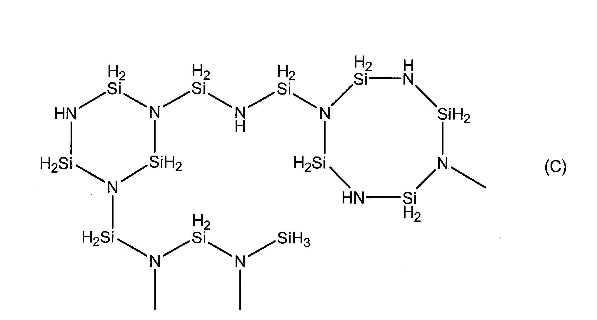
で表される繰り返し単位を有する直鎖状構造を有し、690~2000の分子量を持ち、一分子中に3~10個のSiH3基を有するペルヒドロポリシラザン(特公昭63-16325号公報)、式(A)で表される繰り返し単位を有する、直鎖状構造と分岐構造を有するペルヒドロポリシラザン、又は式(C)で表されるペルヒドロポリシラザン構造を有する、分子内に、直鎖状構造、分岐構造及び環状構造を有するペルヒドロポリシラザン等が挙げられる。
Perhydropolysilazane having a linear structure having a repeating unit represented by formula (II), a molecular weight of 690 to 2000, and 3 to 10 SiH 3 groups in one molecule (Japanese Patent Publication No. 63-16325) A perhydropolysilazane having a linear structure and a branched structure, having a repeating unit represented by the formula (A), or a perhydropolysilazane structure represented by the formula (C), which is linear in the molecule Examples thereof include perhydropolysilazane having a structure, a branched structure, and a cyclic structure.
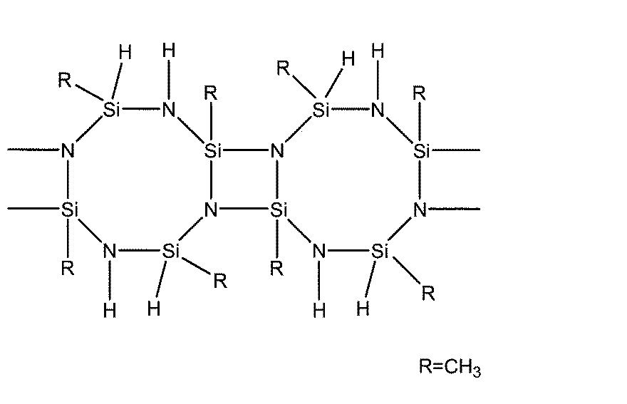
(i)-(Rx´SiHNH)-(Rx´は、無置換若しくは置換基を有するアルキル基、無置換若しくは置換基を有するシクロアルキル基、無置換若しくは置換基を有するアルケニル基、無置換若しくは置換基を有するアリール基、又はアルキルシリル基を表す。以下のRx´も同様である。)を繰り返し単位として、主として重合度が3~5の環状構造を有するもの、
(ii)-(Rx´SiHNRz´)-(Rz´は、無置換若しくは置換基を有するアルキル基、無置換若しくは置換基を有するシクロアルキル基、無置換若しくは置換基を有するアルケニル基、無置換若しくは置換基を有するアリール基、又はアルキルシリル基を表す。)を繰り返し単位として、主として重合度が3~5の環状構造を有するもの、
(iii)-(Rx´Ry´SiNH)-(Ry´は、無置換若しくは置換基を有するアルキル基、無置換若しくは置換基を有するシクロアルキル基、無置換若しくは置換基を有するアルケニル基、無置換若しくは置換基を有するアリール基、又はアルキルシリル基を表す。)を繰り返し単位として、主として重合度が3~5の環状構造を有するもの、
(iv)下記式で表される構造を分子内に有するポリオルガノ(ヒドロ)シラザン、 Examples of the organic polysilazane include the following (i) to (v).
(I) — (Rx′SiHNH) — (Rx ′ is an unsubstituted or substituted alkyl group, an unsubstituted or substituted cycloalkyl group, an unsubstituted or substituted alkenyl group, unsubstituted or substituted An aryl group having a group, or an alkylsilyl group. The following Rx ′ is also the same), and having a cyclic structure having a degree of polymerization of 3 to 5,
(Ii) — (Rx′SiHNRz ′) — (Rz ′) is an unsubstituted or substituted alkyl group, an unsubstituted or substituted cycloalkyl group, an unsubstituted or substituted alkenyl group, unsubstituted or An aryl group having a substituent or an alkylsilyl group) as a repeating unit, mainly having a cyclic structure with a degree of polymerization of 3 to 5,
(Iii) — (Rx′Ry′SiNH) — (Ry ′ is an unsubstituted or substituted alkyl group, unsubstituted or substituted cycloalkyl group, unsubstituted or substituted alkenyl group, unsubstituted Or an aryl group having a substituent or an alkylsilyl group) as a repeating unit, mainly having a cyclic structure with a degree of polymerization of 3 to 5,
(Iv) a polyorgano (hydro) silazane having a structure represented by the following formula in the molecule;
本発明の透明導電性フィルムの基材は、透明導電性フィルムの目的に合致するものであれば特に制限されず、例えばポリイミド、ポリアミド、ポリアミドイミド、ポリフェニレンエーテル、ポリエーテルケトン、ポリエーテルエーテルケトン、ポリオレフィン、ポリエステル、ポリカーボネート、ポリスルフォン、ポリエーテルスルフォン、ポリフェニルサルフォン、変性ポリサルフォン、ポリフェニレンスルフィド、ポリアリレート、アクリル系樹脂、シクロオレフィン系ポリマー、芳香族系重合体、ポリウレタン系ポリマー等が挙げられる。さらに、熱硬化型もしくは放射線硬化型樹脂を用いて熱や放射線で硬化したフィルム等が挙げられる。またこれらに酸化防止剤や難燃剤や高屈折材料や低屈折材料や滑剤等の各種添加剤をガスバリア性、透明性、導電性を損なわない範囲で含んでも良い。 <Base material>
The substrate of the transparent conductive film of the present invention is not particularly limited as long as it meets the purpose of the transparent conductive film. For example, polyimide, polyamide, polyamideimide, polyphenylene ether, polyetherketone, polyetheretherketone, Examples include polyolefin, polyester, polycarbonate, polysulfone, polyethersulfone, polyphenylsulfone, modified polysulfone, polyphenylene sulfide, polyarylate, acrylic resin, cycloolefin polymer, aromatic polymer, polyurethane polymer, and the like. Furthermore, the film etc. which hardened | cured with the heat | fever and the radiation using the thermosetting type or radiation-curable resin are mentioned. These may also contain various additives such as antioxidants, flame retardants, high refractive materials, low refractive materials, and lubricants as long as they do not impair gas barrier properties, transparency, and conductivity.
本発明の透明導電性フィルムは、ガスバリア層上に透明導電膜が積層された構成を特徴とする。透明導電膜を設けることにより、該フィルムに電極としての機能を付与することができ、有機EL表示素子などに好適に使用することができる。透明導電膜の組成としては特に制約はないが、例えば、白金、金、銀、銅等の金属、グラフェン、カーボンナノチューブ等の炭素材料、ポリアリニン、ポリアセチレン、ポリチオフェン、ポリパラフェニレンビニレン、ポリエチレンジオキシチオフェン等の有機導電材料、酸化錫、酸化インジウム、酸化カドミウム、錫ドープ酸化インジウム(ITO)、錫およびガリウムドープ酸化インジウム(IGZO)等の複合酸化物、カルコゲナイド、六ホウ化ランタン、窒化チタン、炭化チタンなどの非酸化化合物、酸化亜鉛、二酸化亜鉛等の酸化物、酸化亜鉛ドープ酸化インジウム、フッ素ドープ酸化インジウム、アンチモンドープ酸化錫、フッ素ドープ酸化錫、アルミニウムドープ酸化亜鉛、ガリウムドープ酸化亜鉛などの酸化亜鉛系導電材料が挙げられる。 <Transparent conductive film>
The transparent conductive film of the present invention is characterized in that a transparent conductive film is laminated on a gas barrier layer. By providing a transparent conductive film, the film can be provided with a function as an electrode and can be suitably used for an organic EL display element or the like. The composition of the transparent conductive film is not particularly limited. For example, metals such as platinum, gold, silver, and copper, graphene, carbon materials such as carbon nanotubes, polyarinin, polyacetylene, polythiophene, polyparaphenylene vinylene, and polyethylenedioxythiophene Organic conductive materials such as tin oxide, indium oxide, cadmium oxide, tin-doped indium oxide (ITO), composite oxides such as tin and gallium-doped indium oxide (IGZO), chalcogenides, lanthanum hexaboride, titanium nitride, titanium carbide Non-oxidized compounds such as zinc oxide, zinc oxide and other oxides, zinc oxide doped indium oxide, fluorine doped indium oxide, antimony doped tin oxide, fluorine doped tin oxide, aluminum doped zinc oxide, gallium doped zinc oxide and other zinc oxide Conductive material And the like.
T1=(R1-R0)/R0
T2=(R2-R0)/R0 In addition, the transparent conductive film of the present invention has an initial sheet resistance value of R 0, and sheet resistance values after being put into a 60 ° C. and 60 ° C. and 90% RH environment for 7 days, respectively, as R 1 and R 2 . When the sheet resistance value change rates T 1 and T 2 are represented by the following formula, T 1 is preferably 1.0 or less, more preferably 0.5 or less, and even more preferably 0.1 or less. T 2 is preferably 1.0 or less, and more preferably 0.2 or less.
T 1 = (R 1 -R 0 ) / R 0
T 2 = (R 2 −R 0 ) / R 0
本発明の透明導電性フィルムの製造方法は、ポリシラザン化合物を含む層を表面に有するフィルムの、前記ポリシラザン化合物を含む層の表層部に、イオンを注入する工程および該イオン注入領域の上に透明導電膜を形成する工程を有することを特徴とする。 2) Method for producing transparent conductive film The method for producing a transparent conductive film of the present invention includes a step of implanting ions into a surface layer portion of a layer containing a polysilazane compound in a film having a layer containing a polysilazane compound on the surface, and It has the process of forming a transparent conductive film on this ion implantation area | region.
本発明の透明導電性フィルムは、優れたガスバリア性と透明導電性を有しているので、電子デバイスに用いた場合、水蒸気等のガスによる素子の劣化を防ぐことができる。また、光の透過性が高いので、タッチパネル、液晶ディスプレイ、ELディスプレイ等のディスプレイ部材;太陽電池用透明電極や有機トランジスタ用電極等として好適である。 3) Electronic device The transparent conductive film of the present invention has excellent gas barrier properties and transparent conductivity, and therefore, when used in an electronic device, it can prevent deterioration of elements due to gas such as water vapor. Moreover, since the light transmittance is high, it is suitable as a display member such as a touch panel, a liquid crystal display, and an EL display;
下記に示す測定条件にて、ガスバリア層の表層部の酸素原子、窒素原子及びケイ素原子の存在割合の測定を行った。
測定装置:「PHI Quantera SXM」アルバックファイ社製
X線ビーム径:100μm
電力値:25W
電圧:15kV
取り出し角度:45° (X-ray photoelectron spectrometer)
Under the measurement conditions shown below, the abundance ratio of oxygen atoms, nitrogen atoms and silicon atoms in the surface layer portion of the gas barrier layer was measured.
Measuring device: “PHI Quantera SXM” ULVAC-PHI X-ray beam diameter: 100 μm
Electric power value: 25W
Voltage: 15kV
Extraction angle: 45 °
ガスバリア層の表層部における膜密度は、下記に示す測定条件にてX線の反射率を測定して全反射臨界角度θcを求め、その値から算出した。
測定装置と測定条件は以下の通りである。
測定装置:薄膜評価用試料水平型X線回折装置「SmartLab」株式会社リガク製
測定条件:
X線源;Cu-Kα1(波長:1.54059Å)
光学系;並行ビーム光学系
入射側スリット系;Ge(220)2結晶、高さ制限スリット5mm、入射スリット0.05mm
受光側スリット系;受光スリット 0.10mm
ソーラースリット 5°
検出器;シンチレーションカウンター
管電圧・管電流;45kV-200mA
走査軸;2θ/θ
走査モード;連続スキャン
走査範囲;0.1-3.0deg.
走査速度;1deg./min.
サンプリング間隔;0.002°/step
なお、原子数比(xi)は、X線光電子分光測定により得られたガスバリア層の表層部における酸素原子、窒素原子及びケイ素原子の存在割合を用いた。 (Measurement method of film density by X-ray reflectivity method)
The film density in the surface layer portion of the gas barrier layer was calculated from the total reflection critical angle θc obtained by measuring the X-ray reflectivity under the following measurement conditions.
The measuring apparatus and measurement conditions are as follows.
Measuring device: Sample horizontal X-ray diffractometer for thin film evaluation “SmartLab” manufactured by Rigaku Corporation Measurement conditions:
X-ray source: Cu-Kα1 (wavelength: 1.54059 mm)
Optical system: Parallel beam optical system Incident side slit system: Ge (220) 2 crystal, height limiting slit 5 mm, incident slit 0.05 mm
Light receiving side slit system; Light receiving slit 0.10mm
Solar slit 5 °
Detector; Scintillation counter Tube voltage and tube current; 45kV-200mA
Scanning axis; 2θ / θ
Scan mode; continuous scan scan range; 0.1-3.0 deg.
Scanning speed: 1 deg. / Min.
Sampling interval; 0.002 ° / step
As the atomic ratio (xi), the ratio of oxygen atoms, nitrogen atoms and silicon atoms in the surface layer portion of the gas barrier layer obtained by X-ray photoelectron spectroscopy was used.
A:ペルヒドロポリシラザンを主成分とするコーティング剤(クラリアントジャパン社製、「アクアミカNL110-20」)
B:飽和炭化水素基を有するオルガノポリシラザン化合物の混合物を主成分とするコーティング材(クラリアントジャパン社製、「tutoProm Bright」) The following A or B was used as the polysilazane compound.
A: Coating agent mainly composed of perhydropolysilazane (manufactured by Clariant Japan, "Aquamica NL110-20")
B: Coating material mainly composed of a mixture of organopolysilazane compounds having a saturated hydrocarbon group (manufactured by Clariant Japan, “tutoProm Bright”)
RF電源:日本電子社製、型番号「RF」56000
高電圧パルス電源:栗田製作所社製、「PV-3-HSHV-0835」 (Plasma ion implantation system)
RF power source: JEOL Ltd., model number “RF” 56000
High voltage pulse power supply: “PV-3-HSHV-0835” manufactured by Kurita Manufacturing Co., Ltd.
透過率測定器:水蒸気透過率が0.01g/m2/day以上のとき、LYSSY社製、「L89-500」を用い、水蒸気透過率が0.01g/m2/day未満のとき、TECHNOLOX社製、「deltaperm」を用いた。
測定条件:相対湿度90%、40℃ (Measurement of water vapor transmission rate)
Transmittance measuring device: When the water vapor transmission rate is 0.01 g / m 2 / day or more, “L89-500” manufactured by LYSSY is used, and when the water vapor transmission rate is less than 0.01 g / m 2 / day, TECHNOLOX “Deltaperm” manufactured by Komatsu Ltd. was used.
Measurement conditions: 90% relative humidity, 40 ° C
可視光透過率測定装置:島津製作所社製、「UV-3101PC」
測定条件:波長550nm (Measurement of visible light transmittance)
Visible light transmittance measuring device: “UV-3101PC” manufactured by Shimadzu Corporation
Measurement conditions: wavelength 550 nm
23℃50%RH環境下で透明導電性フィルムのシート抵抗値(透明導電膜の表面抵抗率)を測定する装置として、「LORESTA―GP MCP-T600」 三菱化学社製を使用した。またプローブは「PROBE TYPE LSP」株式会社三菱化学アナリック社製を用いた。 (Sheet resistance value)
“LORESTA-GP MCP-T600” manufactured by Mitsubishi Chemical Corporation was used as an apparatus for measuring the sheet resistance value of the transparent conductive film (surface resistivity of the transparent conductive film) in an environment of 23 ° C. and 50% RH. The probe used was “PROBE TYPE LSP” manufactured by Mitsubishi Chemical Analytical Corporation.
透明導電性フィルムを60℃および60℃90%RH環境下にそれぞれ7日間投入した。取り出し後、23℃50%RH環境下で1日調温・調湿を行い、シート抵抗値を測定した。投入前のシート抵抗値R0と、60℃7日間投入後のシート抵抗値R1、60℃90%RH7日間投入後のシート抵抗値R2の値から以下のような計算式で評価を行った。ここで、RHとは相対湿度のことをいう。
T1=(R1-R0)/R0
T2=(R2-R0)/R0 (Moisture and heat resistance test)
The transparent conductive film was put in an environment of 60 ° C. and 60 ° C. and 90% RH for 7 days, respectively. After taking out, temperature control and humidity control were performed for one day in an environment of 23 ° C. and 50% RH, and a sheet resistance value was measured. A sheet resistance value R 0 of predose, the evaluation in calculations as follows from the value of the sheet resistance value R 1, 60 ℃ 90% RH7_nichikantonyugonoshitoteikochi R 2 after turned 60 ° C. 7 days conducted It was. Here, RH means relative humidity.
T 1 = (R 1 -R 0 ) / R 0
T 2 = (R 2 −R 0 ) / R 0
基材としてのポリエチレンテレフタレートフィルム(東洋紡績社製、「PET188 A-4300」、厚さ188μm、以下、「PETフィルム」という。)に、ポリシラザン化合物としてAを塗布し、120℃で1分間加熱してPETフィルム上にペルヒドロポリシラザンを含む厚さ60nm(膜厚)の層を形成して成形物を得た。次に、図1に示すプラズマイオン注入装置を用いてペルヒドロポリシラザンを含む層の表面に、アルゴン(Ar)をプラズマイオン注入し、ガスバリア層とした。 Example 1
A polyethylene terephthalate film (“PET188 A-4300” manufactured by Toyobo Co., Ltd., thickness: 188 μm, hereinafter referred to as “PET film”) as a base material was coated with A as a polysilazane compound and heated at 120 ° C. for 1 minute. Then, a 60 nm (thickness) layer containing perhydropolysilazane was formed on the PET film to obtain a molded product. Next, argon (Ar) was ion-implanted into the surface of the layer containing perhydropolysilazane using the plasma ion implantation apparatus shown in FIG. 1 to form a gas barrier layer.
・プラズマ生成ガス:Ar
・ガス流量:100sccm
・Duty比:0.5%
・繰り返し周波数:1000Hz
・印加電圧:-10kV
・RF電源:周波 13.56MHz、印加電力 1000W
・チャンバー内圧:0.2Pa
・パルス幅:5μsec
・処理時間(イオン注入時間):5分間
・搬送速度:0.2m/min. The conditions for plasma ion implantation are shown below.
・ Plasma generated gas: Ar
・ Gas flow rate: 100sccm
・ Duty ratio: 0.5%
・ Repetition frequency: 1000Hz
・ Applied voltage: -10kV
・ RF power supply: frequency 13.56 MHz, applied power 1000 W
-Chamber internal pressure: 0.2 Pa
・ Pulse width: 5μsec
Treatment time (ion implantation time): 5 minutes Transport speed: 0.2 m / min.
・基板温度:室温
・DC出力:500W
・キャリアガス:アルゴン
・真空度:0.3~0.8Paの範囲 The conditions for the transparent conductive film formation step using gallium-doped zinc oxide are shown below.
-Substrate temperature: Room temperature-DC output: 500W
・ Carrier gas: Argon ・ Vacuum degree: 0.3 to 0.8 Pa
加熱時間を1分間から5分間に変更した以外は、実施例1と同様にして実施例2の透明導電性フィルムを得た。 (Example 2)
A transparent conductive film of Example 2 was obtained in the same manner as in Example 1 except that the heating time was changed from 1 minute to 5 minutes.
PETフィルム上に形成するペルヒドロポリシラザンを含む層の厚さを60nmから100nmとした以外は、実施例2と同様にして実施例3の透明導電性フィルムを得た。 (Example 3)
A transparent conductive film of Example 3 was obtained in the same manner as in Example 2 except that the thickness of the layer containing perhydropolysilazane formed on the PET film was changed from 60 nm to 100 nm.
PETフィルム上に形成するペルヒドロポリシラザンを含む層の厚さを60nmから150nmとした以外は、実施例2と同様にして実施例4の透明導電性フィルムを得た。 Example 4
A transparent conductive film of Example 4 was obtained in the same manner as in Example 2 except that the thickness of the layer containing perhydropolysilazane formed on the PET film was changed from 60 nm to 150 nm.
加熱時間を1分間から20分間に変更した以外は、実施例1と同様にして実施例5の透明導電性フィルムを得た。 (Example 5)
A transparent conductive film of Example 5 was obtained in the same manner as in Example 1 except that the heating time was changed from 1 minute to 20 minutes.
プラズマ生成ガスとしてアルゴンに変えて窒素(N2)を用いた以外は、実施例2と同様にして実施例6の透明導電性フィルムを作製した。 (Example 6)
A transparent conductive film of Example 6 was produced in the same manner as in Example 2 except that nitrogen (N 2 ) was used instead of argon as the plasma generating gas.
イオン注入を行う際の印加電圧を-10kVに変えて-5kVとした以外は、実施例2と同様にして実施例7の透明導電性フィルムを作製した。 (Example 7)
A transparent conductive film of Example 7 was produced in the same manner as in Example 2 except that the applied voltage at the time of ion implantation was changed to −10 kV and changed to −5 kV.
イオン注入を行う際の印加電圧を-10kVに変えて-15kVとした以外は、実施例2と同様にして実施例8の透明導電性フィルムを作製した。 (Example 8)
A transparent conductive film of Example 8 was produced in the same manner as Example 2 except that the applied voltage at the time of ion implantation was changed to −10 kV to −15 kV.
ポリシラザン化合物Aの変わりに、ポリシラザン化合物Bを用いた以外は、実施例2と同様にして実施例9の透明導電性フィルムを作製した。 Example 9
A transparent conductive film of Example 9 was produced in the same manner as in Example 2 except that the polysilazane compound B was used instead of the polysilazane compound A.
プラズマ生成ガスとしてアルゴンに変えて水素(H2)を用いた以外は、実施例2と同様にして実施例10の透明導電性フィルムを作製した。 (Example 10)
A transparent conductive film of Example 10 was produced in the same manner as in Example 2 except that hydrogen (H 2 ) was used instead of argon as the plasma generating gas.
プラズマ生成ガスとしてアルゴンに変えて酸素(O2)を用いた以外は、実施例2と同様にして実施例11の透明導電性フィルムを作製した。 (Example 11)
A transparent conductive film of Example 11 was produced in the same manner as Example 2 except that oxygen (O 2 ) was used instead of argon as the plasma generating gas.
プラズマ生成ガスとしてアルゴンに変えてヘリウム(He)を用いた以外は、実施例2と同様にして実施例12の透明導電性フィルムを作製した。 (Example 12)
A transparent conductive film of Example 12 was produced in the same manner as in Example 2 except that helium (He) was used instead of argon as the plasma generation gas.
プラズマ生成ガスとしてアルゴンに変えてネオン(Ne)を用いた以外は、実施例2と同様にして実施例13の透明導電性フィルムを作製した。 (Example 13)
A transparent conductive film of Example 13 was produced in the same manner as Example 2 except that neon (Ne) was used instead of argon as the plasma generating gas.
プラズマ生成ガスとしてアルゴンに変えてキセノン(Xe)を用いた以外は、実施例2と同様にして実施例14の透明導電性フィルムを作製した。 (Example 14)
A transparent conductive film of Example 14 was produced in the same manner as Example 2 except that xenon (Xe) was used instead of argon as the plasma generating gas.
プラズマ生成ガスとしてアルゴンに変えてクリプトン(Kr)を用いた以外は、実施例2と同様にして実施例15の透明導電性フィルムを作製した。 (Example 15)
A transparent conductive film of Example 15 was produced in the same manner as in Example 2 except that krypton (Kr) was used instead of argon as the plasma generating gas.
実施例1に用いたPETフィルムの代わりに基材としてポリエチレンナフタレート(帝人デュポン株式会社製、厚さ200μm,商品名Q65FA)(以下、「PENフィルム」という。)の易接着面にポリシラザン化合物Aを塗布してアルゴンをイオン注入した以外は実施例1と同様に実施例16の透明導電性フィルムを作製した。 (Example 16)
Instead of the PET film used in Example 1, polyethylene naphthalate (made by Teijin DuPont Co., Ltd., thickness: 200 μm, trade name: Q65FA) (hereinafter referred to as “PEN film”) is used as the base material for the polysilazane compound A. A transparent conductive film of Example 16 was produced in the same manner as in Example 1 except that argon was applied and argon was ion-implanted.
実施例1に用いたPETフィルムの代わりに基材として、ポリサルフォン(BASFジャパン株式会社製、製品名「ウルトラゾーンS3010」)を用いて、押出し成形にて厚さ100μmのポリサルフォンフィルムを得た。この得られたポリサルフォンフィルムを使用した以外は実施例1と同様にして、実施例17の透明導電性フィルムを作製した。 (Example 17)
A polysulfone film having a thickness of 100 μm was obtained by extrusion molding using polysulfone (manufactured by BASF Japan Ltd., product name “Ultrazone S3010”) instead of the PET film used in Example 1. A transparent conductive film of Example 17 was produced in the same manner as in Example 1 except that the obtained polysulfone film was used.
実施例1に用いたPETフィルムの代わりに基材として、ポリカーボネート(出光興産株式会社製、製品名「タフロンLC2200」)を用いて、押出し成形にて厚さ100μmのポリカーボネートフィルムを得た。得られたポリカーボネートフィルムを使用した以外は実施例1と同様に実施例18の透明導電性フィルムを作製した。 (Example 18)
A polycarbonate film having a thickness of 100 μm was obtained by extrusion molding using polycarbonate (produced by Idemitsu Kosan Co., Ltd., product name “Taflon LC2200”) instead of the PET film used in Example 1. A transparent conductive film of Example 18 was produced in the same manner as in Example 1 except that the obtained polycarbonate film was used.
実施例1に用いたPETフィルムの代わりに基材として、ポリアリレート(ユニチカ株式会社製 製品名「P-1001」)を用いて、押出し成形にて、厚み100μmのポリアリレートフィルムを得た。得られたポリアリレートフィルムを使用した以外は実施例1と同様に実施例19の透明導電性フィルムを作製した。 (Example 19)
A polyarylate film having a thickness of 100 μm was obtained by extrusion molding using polyarylate (product name “P-1001” manufactured by Unitika Co., Ltd.) as a substrate instead of the PET film used in Example 1. A transparent conductive film of Example 19 was produced in the same manner as Example 1 except that the obtained polyarylate film was used.
実施例1に用いたPETフィルムの代わりに基材として、脂環式炭化水素樹脂フィルム(ゼオン化成社製、厚さ100μm,製品名「ゼオノアZF16」)を使用した以外は実施例1と同様に実施例20の透明導電性フィルムを作製した。 (Example 20)
As in Example 1, except that an alicyclic hydrocarbon resin film (manufactured by Zeon Kasei Co., Ltd., thickness: 100 μm, product name “Zeonor ZF16”) was used as a substrate instead of the PET film used in Example 1. A transparent conductive film of Example 20 was produced.
イオン注入を行わない以外は、実施例1と同様にして比較例1の透明導電性フィルムを作製した。すなわち、PETフィルム上にペルヒドロポリシラザンを含む層を形成しその上に透明導電膜を成膜して比較例1の透明導電性フィルムとした。 (Comparative Example 1)
A transparent conductive film of Comparative Example 1 was produced in the same manner as Example 1 except that ion implantation was not performed. That is, a layer containing perhydropolysilazane was formed on a PET film, and a transparent conductive film was formed thereon to obtain a transparent conductive film of Comparative Example 1.
PETフィルム上にペルヒドロポリシラザンを含む層を形成しない以外は、実施例1と同様にして比較例2の透明導電性フィルムを作製した。すなわち、PETフィルムの表面にアルゴンをプラズマイオン注入して比較例2の透明導電性フィルムとした。 (Comparative Example 2)
A transparent conductive film of Comparative Example 2 was produced in the same manner as in Example 1 except that a layer containing perhydropolysilazane was not formed on the PET film. That is, the transparent conductive film of Comparative Example 2 was obtained by plasma ion implantation of argon on the surface of the PET film.
実施例2で得られた成形物のペルヒドロポリシラザンを含む層にアルゴン(Ar)をプラズマ生成ガスとして用いてプラズマ処理した。そのプラズマ処面に透明導電膜を形成して比較例3の透明導電性フィルムを作製した。プラズマ処理は、実施例で用いた装置の印加電圧を0kVとしてプラズマイオン注入が起きない状態で行った。 (Comparative Example 3)
The layer containing perhydropolysilazane of the molded product obtained in Example 2 was plasma-treated using argon (Ar) as a plasma generation gas. A transparent conductive film was formed on the plasma treated surface to produce a transparent conductive film of Comparative Example 3. The plasma treatment was performed in a state where the applied voltage of the apparatus used in the example was 0 kV and no plasma ion implantation occurred.
・プラズマ生成ガス:Ar
・ガス流量:100sccm
・Duty比:0.5%
・繰り返し周波数:1000Hz
・印加電圧:0kV
・RF電源:周波 13.56MHz、印加電力 1000W
・チャンバー内圧:0.2Pa
・パルス幅:5μsec
・処理時間(イオン注入時間):5分間
・搬送速度:0.2m/min. The conditions for the plasma treatment are shown below.
・ Plasma generated gas: Ar
・ Gas flow rate: 100sccm
・ Duty ratio: 0.5%
・ Repetition frequency: 1000Hz
・ Applied voltage: 0 kV
・ RF power supply: frequency 13.56 MHz, applied power 1000 W
-Chamber internal pressure: 0.2 Pa
・ Pulse width: 5μsec
Treatment time (ion implantation time): 5 minutes Transport speed: 0.2 m / min.

1b、1d・・・フィルム
2a、2b・・・高電圧印加回転キャン
3a、3b・・・巻き出しロール
4・・・プラズマ放電用電極
5a、5b・・・巻き取りロール
6a、6b・・・送り出し用ロール
7a、7b・・・高電圧パルス電源
9a、9b・・・高電圧パルス
10a、10b・・・ガス導入口
11a、11b・・・チャンバー
13・・・中心軸
15・・・高電圧導入端子
20a、20b・・・ターボ分子ポンプ
100・・・透明導電性フィルム
110・・・基材
120・・・ガスバリア層
121・・・イオン注入領域
130・・・透明導電膜 DESCRIPTION OF
Claims (14)
- 基材の少なくとも片面にガスバリア層と、透明導電膜とを具備し、前記ガスバリア層が、少なくとも、酸素原子、窒素原子及びケイ素原子を含む材料から構成されてなり、
前記ガスバリア層の表層部における、酸素原子、窒素原子及びケイ素原子の存在量全体に対する、酸素原子の存在割合が60~75%、窒素原子の存在割合が0~10%、ケイ素原子の存在割合が25~35%であり、かつ、
前記ガスバリア層の表層部における膜密度が、2.4~4.0g/cm3であることを特徴とする透明導電性フィルム。 A gas barrier layer and a transparent conductive film are provided on at least one surface of the base material, and the gas barrier layer is composed of a material containing at least an oxygen atom, a nitrogen atom, and a silicon atom,
In the surface layer portion of the gas barrier layer, the oxygen atom content rate is 60 to 75%, the nitrogen atom content rate is 0 to 10%, and the silicon atom content rate is based on the total abundance of oxygen atoms, nitrogen atoms, and silicon atoms. 25-35%, and
A transparent conductive film, wherein a film density in a surface layer portion of the gas barrier layer is 2.4 to 4.0 g / cm 3 . - 前記ガスバリア層が、ポリシラザン化合物を含むことを特徴とする請求項1に記載の透明導電性フィルム。 The transparent conductive film according to claim 1, wherein the gas barrier layer contains a polysilazane compound.
- 前記ポリシラザン化合物が、ペルヒドロポリシラザンであることを特徴とする請求項1または2に記載の透明導電性フィルム。 The transparent conductive film according to claim 1 or 2, wherein the polysilazane compound is perhydropolysilazane.
- 前記ガスバリア層が、ポリシラザン化合物を含む層にイオンが注入されて得られる層であることを特徴とする請求項1~3のいずれか1項に記載の透明導電性フィルム。 The transparent conductive film according to any one of claims 1 to 3, wherein the gas barrier layer is a layer obtained by implanting ions into a layer containing a polysilazane compound.
- 前記イオンが、水素、窒素、酸素、アルゴン、ヘリウム、ネオン、キセノンおよびクリプトンからなる群から選ばれる少なくとも一種のガスがイオン化されたものであることを特徴とする請求項4に記載の透明導電性フィルム。 5. The transparent conductive material according to claim 4, wherein the ions are ions obtained by ionizing at least one gas selected from the group consisting of hydrogen, nitrogen, oxygen, argon, helium, neon, xenon, and krypton. the film.
- 前記ガスバリア層が、ポリシラザン化合物を含む層に、プラズマイオン注入によりイオンが注入されて得られた層であることを特徴とする請求項4または5に記載の透明導電性フィルム。 6. The transparent conductive film according to claim 4, wherein the gas barrier layer is a layer obtained by implanting ions by plasma ion implantation into a layer containing a polysilazane compound.
- 前記ガスバリア層の40℃、相対湿度90%雰囲気下での水蒸気透過率が0.50g/m2/day未満であることを特徴とする請求項1~6のいずれか1項に記載の透明導電性フィルム。 The transparent conductive material according to any one of claims 1 to 6, wherein the gas barrier layer has a water vapor permeability of less than 0.50 g / m 2 / day in an atmosphere of 40 ° C and a relative humidity of 90%. Sex film.
- 前記透明導電膜が金属酸化物からなる請求項1~7のいずれか1項に記載の透明導電性フィルム。 The transparent conductive film according to any one of claims 1 to 7, wherein the transparent conductive film is made of a metal oxide.
- 前記金属酸化物がインジウム系酸化物もしくは亜鉛系酸化物であり、主成分がそれぞれ酸化インジウムもしくは酸化亜鉛が90質量%以上であることを特徴とする請求項1~8のいずれか1項に記載の透明導電性フィルム。 9. The metal oxide according to claim 1, wherein the metal oxide is an indium oxide or a zinc oxide, and the main component is 90% by mass or more of indium oxide or zinc oxide, respectively. Transparent conductive film.
- ポリシラザン化合物を含む層を表面に有するフィルムの、前記ポリシラザン化合物を含む層の表層部に、イオンを注入する工程と、この上に、透明導電膜を形成する工程とを有する透明導電性フィルムの製造方法。 Production of a transparent conductive film having a step of implanting ions into a surface layer portion of a layer containing a polysilazane compound, and a step of forming a transparent conductive film thereon, of the film having a layer containing a polysilazane compound on the surface Method.
- 前記イオンを注入する工程で、水素、窒素、酸素、アルゴン、ヘリウム、ネオン、キセノンおよびクリプトンからなる群から選ばれる少なくとも一種のガスをイオン注入することを特徴とする請求項10に記載の透明導電性フィルムの製造方法。 11. The transparent conductive material according to claim 10, wherein in the step of implanting ions, at least one gas selected from the group consisting of hydrogen, nitrogen, oxygen, argon, helium, neon, xenon and krypton is ion-implanted. For producing a conductive film.
- 前記イオンを注入する工程で、水素、窒素、酸素、アルゴン、ヘリウム、ネオン、キセノンおよびクリプトンからなる群から選ばれる少なくとも一種のガスをプラズマイオン注入することを特徴とする請求項10に記載の透明導電性フィルムの製造方法。 The transparent ion according to claim 10, wherein at least one gas selected from the group consisting of hydrogen, nitrogen, oxygen, argon, helium, neon, xenon, and krypton is implanted in the ion implantation step. A method for producing a conductive film.
- 前記フィルムがポリシラザン化合物を含む層を表面に有する長尺のフィルムであり、これを一定方向に搬送しながら、前記ポリシラザン化合物を含む層に、イオンを注入することを特徴とする請求項10~12のいずれか1項に記載の透明導電性フィルムの製造方法。 The film is a long film having a layer containing a polysilazane compound on the surface, and ions are implanted into the layer containing the polysilazane compound while conveying the film in a certain direction. The manufacturing method of the transparent conductive film of any one of these.
- 請求項1~9のいずれか1項に記載の透明導電性フィルムを用いたことを特徴とする電子デバイス。 An electronic device comprising the transparent conductive film according to any one of claims 1 to 9.
Priority Applications (5)
| Application Number | Priority Date | Filing Date | Title |
|---|---|---|---|
| US13/576,708 US20120295120A1 (en) | 2010-03-31 | 2011-03-25 | Transparent conductive film, process for producing same, and electronic device employing transparent conductive film |
| CN201180014405.5A CN102811853B (en) | 2010-03-31 | 2011-03-25 | Transparent conductive film, method for producing same, and electronic device using transparent conductive film |
| JP2012508265A JP5404915B2 (en) | 2010-03-31 | 2011-03-25 | Transparent conductive film, method for producing the same, and electronic device using transparent conductive film |
| EP11762728.1A EP2556954B1 (en) | 2010-03-31 | 2011-03-25 | Transparent conductive film and electronic device using transparent conductive film |
| KR1020127022569A KR101382429B1 (en) | 2010-03-31 | 2011-03-25 | Transparent conductive film, method for producing same, and electronic device using transparent conductive film |
Applications Claiming Priority (2)
| Application Number | Priority Date | Filing Date | Title |
|---|---|---|---|
| JP2010-084522 | 2010-03-31 | ||
| JP2010084522 | 2010-03-31 |
Publications (1)
| Publication Number | Publication Date |
|---|---|
| WO2011122497A1 true WO2011122497A1 (en) | 2011-10-06 |
Family
ID=44712203
Family Applications (1)
| Application Number | Title | Priority Date | Filing Date |
|---|---|---|---|
| PCT/JP2011/057459 WO2011122497A1 (en) | 2010-03-31 | 2011-03-25 | Transparent conductive film, method for producing same, and electronic device using transparent conductive film |
Country Status (7)
| Country | Link |
|---|---|
| US (1) | US20120295120A1 (en) |
| EP (1) | EP2556954B1 (en) |
| JP (1) | JP5404915B2 (en) |
| KR (1) | KR101382429B1 (en) |
| CN (1) | CN102811853B (en) |
| TW (1) | TWI492248B (en) |
| WO (1) | WO2011122497A1 (en) |
Cited By (11)
| Publication number | Priority date | Publication date | Assignee | Title |
|---|---|---|---|---|
| WO2013065812A1 (en) * | 2011-11-04 | 2013-05-10 | リンテック株式会社 | Gas barrier film, method for producing same, gas barrier film laminate, member for electronic devices, and electronic device |
| JP2013142941A (en) * | 2012-01-06 | 2013-07-22 | Dainippon Printing Co Ltd | Touch panel member and display device having touch panel member |
| WO2013125351A1 (en) * | 2012-02-21 | 2013-08-29 | リンテック株式会社 | Gas barrier structure and method for forming gas barrier structure |
| KR20140128308A (en) * | 2012-02-21 | 2014-11-05 | 린텍 가부시키가이샤 | Organic electronic element and method for manufacturing organic electronic element |
| KR20140138621A (en) * | 2012-03-22 | 2014-12-04 | 린텍 가부시키가이샤 | Transparent conductive laminate and electronic device or module |
| WO2015118724A1 (en) * | 2014-02-07 | 2015-08-13 | リンテック株式会社 | Transparent conductive laminate, method for producing transparent conductive laminate, and electronic device formed using transparent conductive laminate |
| WO2015118725A1 (en) * | 2014-02-07 | 2015-08-13 | リンテック株式会社 | Transparent conductive film, method for producing transparent conductive film, and electronic device formed using transparent conductive film |
| JP2015147983A (en) * | 2014-02-07 | 2015-08-20 | リンテック株式会社 | Transparent conductive film, method for manufacturing the same and electronic device formed using transparent conductive film |
| WO2016009801A1 (en) * | 2014-07-14 | 2016-01-21 | コニカミノルタ株式会社 | Gas barrier film and electronic device |
| WO2017164209A1 (en) * | 2016-03-23 | 2017-09-28 | 三菱マテリアル株式会社 | Laminated transparent conductive film, laminated wiring film, and method for producing laminated wiring film |
| JP2017179594A (en) * | 2016-03-23 | 2017-10-05 | 三菱マテリアル株式会社 | Laminated transparent conductive film, laminated wiring film, and production method of laminated wiring film |
Families Citing this family (22)
| Publication number | Priority date | Publication date | Assignee | Title |
|---|---|---|---|---|
| US9340869B2 (en) * | 2008-08-19 | 2016-05-17 | Lintec Corporation | Formed article, method for producing the same, electronic device member, and electronic device |
| JP5379530B2 (en) | 2009-03-26 | 2013-12-25 | リンテック株式会社 | Molded body, manufacturing method thereof, electronic device member and electronic device |
| JP5704610B2 (en) | 2009-05-22 | 2015-04-22 | リンテック株式会社 | Molded body, manufacturing method thereof, electronic device member and electronic device |
| JP5697230B2 (en) | 2010-03-31 | 2015-04-08 | リンテック株式会社 | Molded body, manufacturing method thereof, member for electronic device, and electronic device |
| CN103249767B (en) | 2010-08-20 | 2015-05-06 | 琳得科株式会社 | Molding, production method therefor, part for electronic devices and electronic device |
| TWI457235B (en) * | 2010-09-21 | 2014-10-21 | Lintec Corp | A gas barrier film, a manufacturing method thereof, an electronic device element, and an electronic device |
| TWI535561B (en) | 2010-09-21 | 2016-06-01 | Lintec Corp | A molded body, a manufacturing method thereof, an electronic device element, and an electronic device |
| EP2700500A4 (en) | 2011-09-08 | 2015-02-25 | Lintec Corp | Modified polysilazane film and method for producing gas barrier film |
| KR20130078764A (en) * | 2011-12-30 | 2013-07-10 | 코오롱인더스트리 주식회사 | Transparent conductive film |
| WO2013108487A1 (en) | 2012-01-20 | 2013-07-25 | リンテック株式会社 | Gas barrier film and gas barrier film production method |
| JPWO2015037585A1 (en) * | 2013-09-12 | 2017-03-02 | 日本ゼオン株式会社 | Optical element |
| JP6398986B2 (en) * | 2013-10-24 | 2018-10-03 | コニカミノルタ株式会社 | Gas barrier film |
| KR101676522B1 (en) * | 2013-11-29 | 2016-11-15 | 제일모직주식회사 | Gas barrier film and method for preparing the same |
| WO2015118726A1 (en) * | 2014-02-07 | 2015-08-13 | リンテック株式会社 | Transparent conductive laminate, method for producing transparent conductive laminate, and electronic device formed using transparent conductive laminate |
| AU2015288030B2 (en) * | 2014-07-08 | 2020-03-05 | Xyleco, Inc. | Marking plastic-based products |
| US9875987B2 (en) * | 2014-10-07 | 2018-01-23 | Nxp Usa, Inc. | Electronic devices with semiconductor die attached with sintered metallic layers, and methods of formation of such devices |
| GB201515985D0 (en) * | 2015-09-09 | 2015-10-21 | Pilkington Group Ltd | Deposition process |
| KR20170048787A (en) * | 2015-10-27 | 2017-05-10 | 세메스 주식회사 | Apparatus and Method for treating a substrate |
| JP7211740B2 (en) * | 2017-09-13 | 2023-01-24 | 住友化学株式会社 | Gas barrier films and flexible electronic devices |
| CN108873532B (en) * | 2018-06-07 | 2021-03-02 | Tcl华星光电技术有限公司 | Preparation method of three-dimensional electrode |
| WO2019238236A1 (en) * | 2018-06-14 | 2019-12-19 | Applied Materials, Inc. | Roller device for guiding a flexible substrate, use of a roller device for transporting a flexible substrate, vacuum processing apparatus, and method of processing a flexible substrate |
| US11476641B1 (en) * | 2019-06-25 | 2022-10-18 | Mac Thin Films, Inc. | Window for laser protection |
Citations (31)
| Publication number | Priority date | Publication date | Assignee | Title |
|---|---|---|---|---|
| JPS62195024A (en) | 1986-02-12 | 1987-08-27 | Toa Nenryo Kogyo Kk | Polysiloxazane, silicon oxynitride yarn and production thereof |
| JPS6316325B2 (en) | 1983-12-29 | 1988-04-08 | Toa Nenryo Kogyo Kk | |
| JPS6381122A (en) | 1986-09-24 | 1988-04-12 | Toa Nenryo Kogyo Kk | Production of novel polytitanosilazane |
| JPH01138108A (en) | 1987-08-13 | 1989-05-31 | Sekiyu Sangyo Katsuseika Center | Inorganic silazane high-polymer, its production and use thereof |
| JPH0284437A (en) | 1988-03-24 | 1990-03-26 | Tonen Corp | Polyborosilazane and production thereof |
| JPH02175726A (en) | 1988-12-26 | 1990-07-09 | Sekiyu Sangyo Katsuseika Center | Copolysilazane and its production |
| JPH0463833A (en) | 1990-06-30 | 1992-02-28 | Tonen Corp | Modified polysilazane and preparation thereof |
| JPH05238827A (en) | 1992-02-26 | 1993-09-17 | Tonen Corp | Coating composition and coating process |
| JPH05345826A (en) | 1991-12-04 | 1993-12-27 | Tonen Corp | Modified polysilazane and its production |
| JPH0664105A (en) * | 1992-08-12 | 1994-03-08 | Mitsui Toatsu Chem Inc | Gas barrier transparent conductive laminate |
| JPH06122852A (en) | 1992-10-09 | 1994-05-06 | Tonen Corp | Coating composition and method for coating using the same |
| JPH06187833A (en) | 1992-09-11 | 1994-07-08 | Asahi Glass Co Ltd | Transparent conductive film |
| JPH06299118A (en) | 1993-04-20 | 1994-10-25 | Tonen Corp | Coating composition and method for coating |
| JPH06306329A (en) | 1993-02-24 | 1994-11-01 | Tonen Corp | Composition and method for coating |
| JPH0845452A (en) | 1994-08-01 | 1996-02-16 | Takamisawa Denki Seisakusho:Kk | Ion balance measuring device and measuring method for the balance |
| JPH0931333A (en) | 1995-07-13 | 1997-02-04 | Tonen Corp | Composition and method for forming siliceous ceramics and ceramic film made thereof |
| JPH09143289A (en) | 1995-11-20 | 1997-06-03 | Agency Of Ind Science & Technol | Prevention of deterioration of plastic molding material |
| JPH09237159A (en) * | 1995-12-13 | 1997-09-09 | Gunze Ltd | Resistor film type transparent touch panel |
| JPH1034790A (en) * | 1996-07-24 | 1998-02-10 | Mitsui Petrochem Ind Ltd | Laminate |
| JP2000338901A (en) | 1999-06-01 | 2000-12-08 | Matsushita Electric Ind Co Ltd | Manufacture of flexible display substrate |
| JP2001026887A (en) | 1999-07-12 | 2001-01-30 | Agency Of Ind Science & Technol | Surface modifying method and surface modifying device |
| JP2001156013A (en) | 1999-11-26 | 2001-06-08 | Natl Inst Of Advanced Industrial Science & Technology Meti | Method and device for reforming surface |
| JP2006070238A (en) * | 2004-08-05 | 2006-03-16 | Lintec Corp | Method for continuous surface modification of polymer film, apparatus for continuous surface modification and polymer film in which ion injection layer is formed |
| JP2007237588A (en) | 2006-03-09 | 2007-09-20 | Kyodo Printing Co Ltd | Gas-barrier film and method for producing the film |
| JP2008204683A (en) * | 2007-02-19 | 2008-09-04 | Toppan Printing Co Ltd | Transparent conductive film |
| JP2008235165A (en) * | 2007-03-23 | 2008-10-02 | Konica Minolta Holdings Inc | Method of manufacturing roll-like resin film having transparent conductive film |
| JP2008270115A (en) * | 2007-04-25 | 2008-11-06 | Toppan Printing Co Ltd | Transparent conductive gas barrier film |
| JP2009110897A (en) | 2007-11-01 | 2009-05-21 | Toray Ind Inc | Transparent conductive film |
| JP2009199812A (en) | 2008-02-20 | 2009-09-03 | Oike Ind Co Ltd | Base board with transparent conductive film |
| WO2010021326A1 (en) * | 2008-08-19 | 2010-02-25 | リンテック株式会社 | Moulded article, method for producing the same, electronic device member, and electronic device |
| WO2010107018A1 (en) * | 2009-03-17 | 2010-09-23 | リンテック株式会社 | Molded article, process for producing the molded article, member for electronic device, and electronic device |
Family Cites Families (16)
| Publication number | Priority date | Publication date | Assignee | Title |
|---|---|---|---|---|
| US5907382A (en) * | 1994-12-20 | 1999-05-25 | Kabushiki Kaisha Toshiba | Transparent conductive substrate and display apparatus |
| US5965629A (en) * | 1996-04-19 | 1999-10-12 | Korea Institute Of Science And Technology | Process for modifying surfaces of materials, and materials having surfaces modified thereby |
| CN1237199C (en) * | 2000-06-21 | 2006-01-18 | 日本板硝子株式会社 | Substrate with transperant conductive film and organic electroluminescence device using the substrate |
| US6962756B2 (en) * | 2001-11-02 | 2005-11-08 | Mitsubishi Gas Chemical Company, Inc. | Transparent electrically-conductive film and its use |
| KR100483988B1 (en) * | 2001-11-29 | 2005-04-15 | 삼성에스디아이 주식회사 | Method of Varying Transmittance in transparent conductive film |
| JP3971639B2 (en) * | 2002-04-18 | 2007-09-05 | 大日本印刷株式会社 | Barrier film, laminated material using the same, packaging container, image display medium, and barrier film manufacturing method |
| JP4261902B2 (en) * | 2002-12-26 | 2009-05-13 | 大日本印刷株式会社 | Barrier film and laminate using the same, packaging container, image display medium, and barrier film manufacturing method |
| US7898010B2 (en) * | 2004-07-01 | 2011-03-01 | Micron Technology, Inc. | Transparent conductor based pinned photodiode |
| JP4716773B2 (en) * | 2005-04-06 | 2011-07-06 | 富士フイルム株式会社 | Gas barrier film and organic device using the same |
| KR20090001922A (en) * | 2007-05-29 | 2009-01-09 | 주식회사 신한은행 | System and method for judging auto-delaying of giving credit and program recording medium |
| TW200903710A (en) * | 2007-07-11 | 2009-01-16 | Promos Technologies Inc | Manufacturing method for shallow trench isolation |
| WO2009054464A1 (en) * | 2007-10-26 | 2009-04-30 | Teijin Limited | Transparent conductive laminate and transparent touch panel |
| JP5069582B2 (en) * | 2008-02-05 | 2012-11-07 | 有限会社コンタミネーション・コントロール・サービス | Method for forming silica film |
| JP5297125B2 (en) * | 2008-09-09 | 2013-09-25 | グンゼ株式会社 | Gas barrier film with transparent conductive film and touch panel using the same |
| CN102245379B (en) * | 2008-12-12 | 2015-06-24 | 琳得科株式会社 | Laminate, method for producing same, electronic device member, and electronic device |
| JP5566130B2 (en) * | 2009-02-26 | 2014-08-06 | キヤノン株式会社 | Method for manufacturing liquid discharge head |
-
2011
- 2011-03-25 WO PCT/JP2011/057459 patent/WO2011122497A1/en active Application Filing
- 2011-03-25 US US13/576,708 patent/US20120295120A1/en not_active Abandoned
- 2011-03-25 EP EP11762728.1A patent/EP2556954B1/en active Active
- 2011-03-25 JP JP2012508265A patent/JP5404915B2/en active Active
- 2011-03-25 KR KR1020127022569A patent/KR101382429B1/en active IP Right Grant
- 2011-03-25 CN CN201180014405.5A patent/CN102811853B/en active Active
- 2011-03-31 TW TW100111311A patent/TWI492248B/en active
Patent Citations (31)
| Publication number | Priority date | Publication date | Assignee | Title |
|---|---|---|---|---|
| JPS6316325B2 (en) | 1983-12-29 | 1988-04-08 | Toa Nenryo Kogyo Kk | |
| JPS62195024A (en) | 1986-02-12 | 1987-08-27 | Toa Nenryo Kogyo Kk | Polysiloxazane, silicon oxynitride yarn and production thereof |
| JPS6381122A (en) | 1986-09-24 | 1988-04-12 | Toa Nenryo Kogyo Kk | Production of novel polytitanosilazane |
| JPH01138108A (en) | 1987-08-13 | 1989-05-31 | Sekiyu Sangyo Katsuseika Center | Inorganic silazane high-polymer, its production and use thereof |
| JPH0284437A (en) | 1988-03-24 | 1990-03-26 | Tonen Corp | Polyborosilazane and production thereof |
| JPH02175726A (en) | 1988-12-26 | 1990-07-09 | Sekiyu Sangyo Katsuseika Center | Copolysilazane and its production |
| JPH0463833A (en) | 1990-06-30 | 1992-02-28 | Tonen Corp | Modified polysilazane and preparation thereof |
| JPH05345826A (en) | 1991-12-04 | 1993-12-27 | Tonen Corp | Modified polysilazane and its production |
| JPH05238827A (en) | 1992-02-26 | 1993-09-17 | Tonen Corp | Coating composition and coating process |
| JPH0664105A (en) * | 1992-08-12 | 1994-03-08 | Mitsui Toatsu Chem Inc | Gas barrier transparent conductive laminate |
| JPH06187833A (en) | 1992-09-11 | 1994-07-08 | Asahi Glass Co Ltd | Transparent conductive film |
| JPH06122852A (en) | 1992-10-09 | 1994-05-06 | Tonen Corp | Coating composition and method for coating using the same |
| JPH06306329A (en) | 1993-02-24 | 1994-11-01 | Tonen Corp | Composition and method for coating |
| JPH06299118A (en) | 1993-04-20 | 1994-10-25 | Tonen Corp | Coating composition and method for coating |
| JPH0845452A (en) | 1994-08-01 | 1996-02-16 | Takamisawa Denki Seisakusho:Kk | Ion balance measuring device and measuring method for the balance |
| JPH0931333A (en) | 1995-07-13 | 1997-02-04 | Tonen Corp | Composition and method for forming siliceous ceramics and ceramic film made thereof |
| JPH09143289A (en) | 1995-11-20 | 1997-06-03 | Agency Of Ind Science & Technol | Prevention of deterioration of plastic molding material |
| JPH09237159A (en) * | 1995-12-13 | 1997-09-09 | Gunze Ltd | Resistor film type transparent touch panel |
| JPH1034790A (en) * | 1996-07-24 | 1998-02-10 | Mitsui Petrochem Ind Ltd | Laminate |
| JP2000338901A (en) | 1999-06-01 | 2000-12-08 | Matsushita Electric Ind Co Ltd | Manufacture of flexible display substrate |
| JP2001026887A (en) | 1999-07-12 | 2001-01-30 | Agency Of Ind Science & Technol | Surface modifying method and surface modifying device |
| JP2001156013A (en) | 1999-11-26 | 2001-06-08 | Natl Inst Of Advanced Industrial Science & Technology Meti | Method and device for reforming surface |
| JP2006070238A (en) * | 2004-08-05 | 2006-03-16 | Lintec Corp | Method for continuous surface modification of polymer film, apparatus for continuous surface modification and polymer film in which ion injection layer is formed |
| JP2007237588A (en) | 2006-03-09 | 2007-09-20 | Kyodo Printing Co Ltd | Gas-barrier film and method for producing the film |
| JP2008204683A (en) * | 2007-02-19 | 2008-09-04 | Toppan Printing Co Ltd | Transparent conductive film |
| JP2008235165A (en) * | 2007-03-23 | 2008-10-02 | Konica Minolta Holdings Inc | Method of manufacturing roll-like resin film having transparent conductive film |
| JP2008270115A (en) * | 2007-04-25 | 2008-11-06 | Toppan Printing Co Ltd | Transparent conductive gas barrier film |
| JP2009110897A (en) | 2007-11-01 | 2009-05-21 | Toray Ind Inc | Transparent conductive film |
| JP2009199812A (en) | 2008-02-20 | 2009-09-03 | Oike Ind Co Ltd | Base board with transparent conductive film |
| WO2010021326A1 (en) * | 2008-08-19 | 2010-02-25 | リンテック株式会社 | Moulded article, method for producing the same, electronic device member, and electronic device |
| WO2010107018A1 (en) * | 2009-03-17 | 2010-09-23 | リンテック株式会社 | Molded article, process for producing the molded article, member for electronic device, and electronic device |
Non-Patent Citations (1)
| Title |
|---|
| See also references of EP2556954A4 |
Cited By (28)
| Publication number | Priority date | Publication date | Assignee | Title |
|---|---|---|---|---|
| KR20200006168A (en) * | 2011-11-04 | 2020-01-17 | 린텍 가부시키가이샤 | Gas barrier film, method for producing same, gas barrier film laminate, member for electronic devices, and electronic device |
| WO2013065812A1 (en) * | 2011-11-04 | 2013-05-10 | リンテック株式会社 | Gas barrier film, method for producing same, gas barrier film laminate, member for electronic devices, and electronic device |
| CN107953623A (en) * | 2011-11-04 | 2018-04-24 | 琳得科株式会社 | Gas barrier film and its manufacture method, gas barrier film stack, use for electronic equipment component and electronic device |
| KR20140079803A (en) * | 2011-11-04 | 2014-06-27 | 린텍 가부시키가이샤 | Gas barrier film, method for producing same, gas barrier film laminate, member for electronic devices, and electronic device |
| CN104066576A (en) * | 2011-11-04 | 2014-09-24 | 琳得科株式会社 | Gas barrier film, method for producing same, gas barrier film laminate, member for electronic devices, and electronic device |
| KR102064143B1 (en) * | 2011-11-04 | 2020-01-08 | 린텍 가부시키가이샤 | Gas barrier film, method for producing same, gas barrier film laminate, member for electronic devices, and electronic device |
| KR102168722B1 (en) * | 2011-11-04 | 2020-10-22 | 린텍 가부시키가이샤 | Gas barrier film, method for producing same, gas barrier film laminate, member for electronic devices, and electronic device |
| JPWO2013065812A1 (en) * | 2011-11-04 | 2015-04-02 | リンテック株式会社 | GAS BARRIER FILM AND MANUFACTURING METHOD THEREOF, GAS BARRIER FILM LAMINATE, ELECTRONIC DEVICE MEMBER, AND ELECTRONIC DEVICE |
| JP2013142941A (en) * | 2012-01-06 | 2013-07-22 | Dainippon Printing Co Ltd | Touch panel member and display device having touch panel member |
| JP5408818B1 (en) * | 2012-02-21 | 2014-02-05 | リンテック株式会社 | Gas barrier structure and method for forming gas barrier structure |
| KR20140128308A (en) * | 2012-02-21 | 2014-11-05 | 린텍 가부시키가이샤 | Organic electronic element and method for manufacturing organic electronic element |
| EP2819486B1 (en) * | 2012-02-21 | 2019-11-13 | LINTEC Corporation | Method for manufacturing organic electronic element |
| KR102039390B1 (en) * | 2012-02-21 | 2019-11-04 | 린텍 가부시키가이샤 | Organic electronic element and method for manufacturing organic electronic element |
| WO2013125351A1 (en) * | 2012-02-21 | 2013-08-29 | リンテック株式会社 | Gas barrier structure and method for forming gas barrier structure |
| KR102005598B1 (en) * | 2012-03-22 | 2019-07-30 | 린텍 가부시키가이샤 | Transparent conductive laminate and electronic device or module |
| KR20140138621A (en) * | 2012-03-22 | 2014-12-04 | 린텍 가부시키가이샤 | Transparent conductive laminate and electronic device or module |
| WO2015118725A1 (en) * | 2014-02-07 | 2015-08-13 | リンテック株式会社 | Transparent conductive film, method for producing transparent conductive film, and electronic device formed using transparent conductive film |
| JPWO2015119239A1 (en) * | 2014-02-07 | 2017-03-30 | リンテック株式会社 | Transparent conductive film, method for producing transparent conductive film, and electronic device using transparent conductive film |
| JP2015147983A (en) * | 2014-02-07 | 2015-08-20 | リンテック株式会社 | Transparent conductive film, method for manufacturing the same and electronic device formed using transparent conductive film |
| WO2015119239A1 (en) * | 2014-02-07 | 2015-08-13 | リンテック株式会社 | Transparent conductive film, method for producing transparent conductive film, and electronic device formed using transparent conductive film |
| WO2015118724A1 (en) * | 2014-02-07 | 2015-08-13 | リンテック株式会社 | Transparent conductive laminate, method for producing transparent conductive laminate, and electronic device formed using transparent conductive laminate |
| KR101905298B1 (en) | 2014-07-14 | 2018-10-05 | 코니카 미놀타 가부시키가이샤 | Gas barrier film and electronic device |
| WO2016009801A1 (en) * | 2014-07-14 | 2016-01-21 | コニカミノルタ株式会社 | Gas barrier film and electronic device |
| JPWO2016009801A1 (en) * | 2014-07-14 | 2017-04-27 | コニカミノルタ株式会社 | Gas barrier film and electronic device |
| JP2017179594A (en) * | 2016-03-23 | 2017-10-05 | 三菱マテリアル株式会社 | Laminated transparent conductive film, laminated wiring film, and production method of laminated wiring film |
| KR20180126470A (en) * | 2016-03-23 | 2018-11-27 | 미쓰비시 마테리알 가부시키가이샤 | A laminated transparent conductive film, a laminated wiring film, and a method for manufacturing a laminated wiring film |
| WO2017164209A1 (en) * | 2016-03-23 | 2017-09-28 | 三菱マテリアル株式会社 | Laminated transparent conductive film, laminated wiring film, and method for producing laminated wiring film |
| KR102333536B1 (en) * | 2016-03-23 | 2021-11-30 | 미쓰비시 마테리알 가부시키가이샤 | Manufacturing method of laminated transparent conductive film, laminated wiring film, and laminated wiring film |
Also Published As
| Publication number | Publication date |
|---|---|
| JPWO2011122497A1 (en) | 2013-07-08 |
| CN102811853A (en) | 2012-12-05 |
| KR20120123115A (en) | 2012-11-07 |
| CN102811853B (en) | 2015-05-20 |
| US20120295120A1 (en) | 2012-11-22 |
| KR101382429B1 (en) | 2014-04-08 |
| EP2556954A4 (en) | 2013-09-04 |
| TWI492248B (en) | 2015-07-11 |
| EP2556954B1 (en) | 2019-09-25 |
| TW201222567A (en) | 2012-06-01 |
| EP2556954A1 (en) | 2013-02-13 |
| JP5404915B2 (en) | 2014-02-05 |
Similar Documents
| Publication | Publication Date | Title |
|---|---|---|
| JP5404915B2 (en) | Transparent conductive film, method for producing the same, and electronic device using transparent conductive film | |
| JP4956692B1 (en) | Molded body, manufacturing method thereof, member for electronic device, and electronic device | |
| JP5808747B2 (en) | Molded body, manufacturing method thereof, member for electronic device, and electronic device | |
| JP5372240B2 (en) | Transparent conductive film, method for producing the same, and electronic device using transparent conductive film | |
| EP2620278B1 (en) | Gas-barrier film, process for producing same, member for electronic device, and electronic device | |
| EP2433980B1 (en) | Molded object, process for producing same, member for electronic device, and electronic device | |
| EP2830068B1 (en) | Transparent conductive laminate and electronic device or module | |
| WO2012050160A1 (en) | Transparent conductive film, production method therefor, material for electronic device, and electronic device | |
| JP5781350B2 (en) | GAS BARRIER LAMINATE, ITS MANUFACTURING METHOD, ELECTRONIC DEVICE MEMBER AND ELECTRONIC DEVICE |
Legal Events
| Date | Code | Title | Description |
|---|---|---|---|
| WWE | Wipo information: entry into national phase |
Ref document number: 201180014405.5 Country of ref document: CN |
|
| 121 | Ep: the epo has been informed by wipo that ep was designated in this application |
Ref document number: 11762728 Country of ref document: EP Kind code of ref document: A1 |
|
| WWE | Wipo information: entry into national phase |
Ref document number: 2012508265 Country of ref document: JP |
|
| WWE | Wipo information: entry into national phase |
Ref document number: 13576708 Country of ref document: US |
|
| WWE | Wipo information: entry into national phase |
Ref document number: 2011762728 Country of ref document: EP |
|
| ENP | Entry into the national phase |
Ref document number: 20127022569 Country of ref document: KR Kind code of ref document: A |
|
| NENP | Non-entry into the national phase |
Ref country code: DE |