WO2011122323A1 - 可変分光素子 - Google Patents
可変分光素子 Download PDFInfo
- Publication number
- WO2011122323A1 WO2011122323A1 PCT/JP2011/055995 JP2011055995W WO2011122323A1 WO 2011122323 A1 WO2011122323 A1 WO 2011122323A1 JP 2011055995 W JP2011055995 W JP 2011055995W WO 2011122323 A1 WO2011122323 A1 WO 2011122323A1
- Authority
- WO
- WIPO (PCT)
- Prior art keywords
- pair
- opposing surfaces
- optical substrates
- gravity
- centers
- Prior art date
- Legal status (The legal status is an assumption and is not a legal conclusion. Google has not performed a legal analysis and makes no representation as to the accuracy of the status listed.)
- Ceased
Links
Images


Classifications
-
- G—PHYSICS
- G01—MEASURING; TESTING
- G01B—MEASURING LENGTH, THICKNESS OR SIMILAR LINEAR DIMENSIONS; MEASURING ANGLES; MEASURING AREAS; MEASURING IRREGULARITIES OF SURFACES OR CONTOURS
- G01B7/00—Measuring arrangements characterised by the use of electric or magnetic techniques
- G01B7/003—Measuring arrangements characterised by the use of electric or magnetic techniques for measuring position, not involving coordinate determination
-
- G—PHYSICS
- G01—MEASURING; TESTING
- G01B—MEASURING LENGTH, THICKNESS OR SIMILAR LINEAR DIMENSIONS; MEASURING ANGLES; MEASURING AREAS; MEASURING IRREGULARITIES OF SURFACES OR CONTOURS
- G01B7/00—Measuring arrangements characterised by the use of electric or magnetic techniques
- G01B7/30—Measuring arrangements characterised by the use of electric or magnetic techniques for measuring angles or tapers; for testing the alignment of axes
-
- G—PHYSICS
- G01—MEASURING; TESTING
- G01J—MEASUREMENT OF INTENSITY, VELOCITY, SPECTRAL CONTENT, POLARISATION, PHASE OR PULSE CHARACTERISTICS OF INFRARED, VISIBLE OR ULTRAVIOLET LIGHT; COLORIMETRY; RADIATION PYROMETRY
- G01J3/00—Spectrometry; Spectrophotometry; Monochromators; Measuring colours
- G01J3/12—Generating the spectrum; Monochromators
- G01J3/26—Generating the spectrum; Monochromators using multiple reflection, e.g. Fabry-Perot interferometer, variable interference filters
-
- G—PHYSICS
- G02—OPTICS
- G02B—OPTICAL ELEMENTS, SYSTEMS OR APPARATUS
- G02B26/00—Optical devices or arrangements for the control of light using movable or deformable optical elements
- G02B26/001—Optical devices or arrangements for the control of light using movable or deformable optical elements based on interference in an adjustable optical cavity
Definitions
- the present invention relates to a variable spectroscopic element.
- a capacitance sensor for measuring the surface interval is arranged on the opposite surface, and the capacitance A sensor that measures the current surface interval at a predetermined sampling cycle, compares the measured surface interval with the desired surface interval, and drives the actuator based on the comparison result to adjust the surface interval.
- Known for example, see JP-A-6-241899.
- variable spectroscopic element as described in Japanese Patent Application Laid-Open No. 2008-129149 and Japanese Patent Application Laid-Open No. 6-241899 is used, for example, in a spectroscopic endoscope apparatus that acquires an image whose spectral characteristics are continuously changed.
- the surface distance of the optical substrate must be changed by controlling the actuator within a very short time of one frame of the sampling period of image acquisition. .
- variable spectroscopic element as described in Japanese Patent Application Laid-Open No. 2008-129149 and Japanese Patent Application Laid-Open No. 6-241899 are as follows. Actuator control must be accurate because it is greatly affected by the degree.
- the present invention has been made in view of such problems of the prior art, and an object thereof is to provide a variable spectroscopic element capable of changing optical characteristics at high speed and accurately.
- variable spectroscopic element of the present invention is disposed on each of a pair of optical substrates disposed so as to face each other with a space therebetween, and each of the facing surfaces of the pair of optical substrates. At least one of the pair of optical substrates and the first to fourth capacitance sensors that detect a surface interval between the opposing surfaces of the pair of optical substrates at each arrangement position.
- the first capacitance sensor and the third capacitance sensor is disposed at a position that is symmetric with respect to a line connecting the centers of gravity of the opposing surfaces of the pair of optical substrates, and the second capacitance sensor and the fourth capacitance sensor.
- Capacitance sensor Each of the first to fourth actuators is disposed on a position symmetrical with respect to a line connecting the centers of gravity of the opposing surfaces of the pair of optical substrates, and each of the first to fourth actuators Each of the first to fourth capacitance sensors is arranged on a line extending from the center of gravity to the center of each of the first to fourth capacitance sensors. The signals from the first to fourth capacitance sensors are opposed to the pair of optical substrates.
- the optical substrate that calculates the distance between the centroids of the surfaces to be moved and moves to a plane perpendicular to the line connecting the centroids from the signal from the first capacitance sensor and the signal from the third capacitance sensor
- the first angle formed by the opposing surfaces of the first and second surfaces is calculated and moved from a signal perpendicular to the line connecting the centers of gravity based on the signal from the second capacitance sensor and the signal from the fourth capacitance sensor.
- the facing of the optical substrate And calculating the second angle formed by the surface to be driven, driving the first and third actuators based on the distance between the centroids and the first angle, and setting the distance between the centroids and the second angle. And a controller for driving the second and third actuators.
- each of the first to fourth capacitance sensors and each of the first to fourth actuators connects the centers of gravity of the opposing surfaces of the pair of optical substrates. It is preferably arranged at an overlapping position when viewed from the direction along the axis with the elliptical line as an axis, and satisfies the following conditional expression.
- x 1 , x 2 , x 3 and x 4 are the distances between the pair of optical substrates at the positions where the first to fourth capacitance sensors are arranged
- ⁇ is the first distance.
- An angle of 1, ⁇ is the second angle
- r is a distance from the center of gravity on the opposing surface of the movable substrate to the capacitance sensor.
- control unit may determine the distance between the centroids based on the average of the surface distances between the opposing surfaces of the pair of optical substrates at the positions where the first to fourth capacitance sensors are disposed.
- first angle is calculated from the difference in surface spacing between the opposing surfaces of the pair of optical substrates at the positions where the first and third capacitance sensors are arranged, and the second and fourth static sensors are calculated. It is preferable that the second angle is calculated from a difference in surface interval between the opposing surfaces of the pair of optical substrates at the position where the capacitance sensor is disposed.
- each of the first to fourth capacitance sensors and each of the first to fourth actuators connects the centers of gravity of the opposing surfaces of the pair of optical substrates. It is preferably arranged at a position overlapping with the line as an axis when viewed from the direction along the axis, and the following conditional expression is satisfied.
- x is the distance between the centers of gravity
- x 1 , x 2 , x 3 and x 4 are the distances between the opposing surfaces of the pair of optical substrates at the positions where the first to fourth capacitance sensors are arranged.
- ⁇ is the first angle
- ⁇ is the second angle
- R 1 and R 2 are predetermined coefficients.
- variable spectroscopic element of the present invention includes a pair of optical substrates disposed so as to be opposed to each other with a gap therebetween, and a surface facing each of the pair of optical substrates.
- First to fourth capacitance sensors having a pair of arranged electrode portions and detecting a surface interval between the opposed surfaces of the pair of optical substrates at the respective disposed positions; and
- the first capacitance sensor And the third capacitance sensor are arranged at positions symmetrical with respect to a line connecting the centers of gravity of the opposing surfaces of the pair of optical substrates, and the second capacitance sensor and the third capacitance sensor With the fourth capacitance sensor
- the first to fourth capacitance sensors and the first to fourth actuators are arranged symmetrically with respect to a line connecting the centers of gravity of the opposing surfaces of the pair of optical substrates.
- the first to fourth static plates are arranged annularly so as to be alternately spaced from each other with a line connecting the centers of gravity of the opposing surfaces of the pair of optical substrates as an axis.
- a first angle formed by a surface perpendicular to a line connecting the centers of gravity and the opposed surfaces of the optical substrate to be moved is calculated using a value of a surface interval between the opposed surfaces of the pair of optical substrates at a position.
- variable spectroscopic element capable of changing an optical characteristic at high speed and accurately.
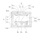
- FIG. 1 is a cross-sectional view illustrating the etalon device of the variable spectral element according to the first embodiment.
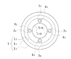
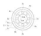
- FIG. 2 is a plan view of the etalon device of FIG.
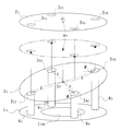
- FIG. 3 is a schematic diagram showing the operation of a pair of optical substrates and four piezoelectric elements of the etalon device of FIG.
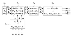
- FIG. 4 is a block diagram illustrating calculation performed by the control unit of the variable spectral element according to the first embodiment.
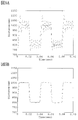
- FIG. 5 is a graph showing response characteristics of the etalon device of FIG. 1, FIG. 5A is a graph when controlled by a conventional variable spectroscopic element, and 5B is a graph when controlled by the variable spectroscopic element of this embodiment. .
- FIG. 1 is a cross-sectional view illustrating the etalon device of the variable spectral element according to the first embodiment.
- FIG. 2 is a plan view of the etalon device of FIG.
- FIG. 3 is a schematic diagram showing the
- FIG. 6 is a plan view showing a first modification of the etalon device of FIG.
- FIG. 7 is a plan view showing a second modification of the etalon device of FIG.
- FIG. 8 is a plan view showing a third modification of the etalon device of FIG.
- FIG. 9 is a sectional view showing a fourth modification of the etalon device of FIG.
- FIG. 10 is a cross-sectional view illustrating the etalon device of the variable spectral element according to the second embodiment.
- FIG. 11 is a plan view of the etalon device of FIG.
- variable spectroscopic element A first embodiment of the variable spectroscopic element according to the present invention will be described with reference to FIGS. 1 to 5, and thereafter, four modified examples will be described with reference to FIGS.
- FIG. 1 is a sectional view showing an etalon device for a variable spectroscopic element according to the present embodiment.
- FIG. 2 is a plan view of the etalon device of FIG.
- FIG. 3 is a schematic diagram showing the operation of a pair of optical substrates and four piezoelectric elements of the etalon device of FIG.
- FIG. 4 is a block diagram illustrating the calculation performed by the control unit of the variable spectral element according to the first embodiment.
- 5 is a graph showing response characteristics of the etalon device of FIG. 1, FIG. 5A is a graph when controlled by a conventional variable spectroscopic element, and FIG. 5B is a graph when controlled by a variable spectroscopic element of this embodiment. It is.
- FIG. 5A is a graph when controlled by a conventional variable spectroscopic element
- FIG. 5B is a graph when controlled by a variable spectroscopic element of this embodiment. It is.
- FIG. 5A is a graph when controlled by
- FIG. 6 is a plan view showing a first modification of the etalon device of FIG.
- FIG. 7 is a plan view showing a second modification of the etalon device of FIG.
- FIG. 8 is a plan view showing a third modification of the etalon device of FIG.
- FIG. 9 is a cross-sectional view showing a fourth modification of the etalon device of FIG.
- variable spectroscopic element is configured by the etalon device shown in FIGS. 1 and 2 and a control unit (not shown).
- this etalon device includes a pair of optical substrates 2 in the outer frame 1 and a capacitance that is a means for measuring a surface interval between the opposing surfaces of the pair of optical substrates 2.
- the sensor is an actuator for moving one of the pair of optical substrates 2 and includes a piezoelectric element whose driving is controlled by a control unit (not shown).
- the outer frame 1, the annular member 1 2 in one end surface of the tubular member 1 1 is constituted by attaching the annular member 1 3 on the other.
- circular openings 1 2 a and 1 3 a are formed in the annular members 1 2 and 1 3 at substantially the center thereof. In this etalon device, the openings 1 2 a and 1 3 are formed. Light passes through a.
- the pair of optical substrates 2 includes a fixed substrate 2 1 and a movable substrate 2 2 that are arranged so that opposing surfaces are parallel to each other with a space therebetween.
- the fixed substrate 2 1 the opening 1 2 a in the interior of the outer frame 1, 1 3 disc which is fixed to the annular member 1 2 of the outer frame 1 so as to cross the axis of the light passing through the a Shaped optical member.
- the movable substrate 2 2 is a disc-shaped optical member held by the piezo element so as to cross the light passing through the openings 1 2 a and 1 3 a.
- the movable substrate 2 2 has a direction along the axis of light passing through the openings 1 2 a and 1 3 a, that is, the center of gravity of each of the opposing surfaces of the pair of optical substrates.
- the first capacitance sensor 3 1 , the second capacitance sensor 3 2 , the third capacitance sensor 3 3 , and the fourth capacitance sensor 3 4 have a pair of electrodes 3 11 , 3 12 , 3 21 , respectively. And 3 22 , 3 31 and 3 32 , 3 41 and 3 42 .
- the pair of electrodes are opposed to each other at positions where the light passing through the openings 1 2 a and 1 3 a of the outer frame 1 is not blocked on the opposing surfaces of the pair of optical substrates 2. are arranged.
- these capacitance sensors have a characteristic that the capacitance between the electrodes changes in inverse proportion to the surface spacing.
- the value acquired by these capacitance sensors is converted into the surface interval value of the optical substrate 2 and output to a control unit (not shown).
- the first piezo element 4 1 , the second piezo element 4 2 , the third piezo element 4 3 , and the fourth piezo element 4 4 respectively transmit the light passing through the openings 1 2 a and 1 3 a inside the outer frame 1. It is fixed to the annular member 1 3 of the outer frame 1 so as not to block.
- the first piezo element 4 1 is the first capacitance sensor 3 1
- the second piezo element 4 2 is the second capacitance sensor 3 2
- the third piezo element 4 3 is the third capacitance sensor 3.
- the fourth piezo element 4 4 are arranged at an overlapping position when viewed from the direction along the line connecting the centroids of the surfaces of the fourth electrostatic capacitance sensor 3 4 and the pair of optical substrates 2 facing each other. .
- the first capacitance sensor 3 1 and the first piezo element 4 1 , and the third capacitance sensor 3 3 and the third piezo element 4 3 are respectively centroids of the opposing surfaces of the pair of optical substrates 2. As viewed from the direction along the line connecting the centroids, they are arranged at positions symmetrical with respect to the line connecting the centers of gravity.
- the second capacitance sensor 3 2 and the second piezo element 4 2 , and the fourth capacitance sensor 3 4 and the fourth piezo element 4 4 are respectively centroids of the opposing surfaces of the pair of optical substrates 2. As viewed from the direction along the line connecting the centroids, they are arranged at positions symmetrical with respect to the line connecting the centers of gravity.
- the first capacitance sensor 3 1 and the first piezo element 4 1 , the second capacitance sensor 3 2 and the second piezo element 4 2 , the third capacitance sensor 3 3 and the third piezo element 4. 3 and the fourth capacitance sensor 3 4 and the fourth piezo element 4 4 are arranged at equal intervals as viewed from the direction along the line connecting the centers of gravity of the opposing surfaces of the pair of optical substrates 2. Yes.
- the second piezoelectric element 4 2 based on the second capacitive sensor 3 and second output values, based on the output value of the third capacitive sensor 3 3 the third piezoelectric element 4 3 had fourth drives the piezoelectric elements 4 4 based on the output value of the fourth capacitive sensors 3 4.
- the first piezo element 4 1 is accurately driven, and the surface interval of the pair of optical substrates 2 at the arrangement position of the first capacitance sensor 3 1 is set to the target value x o. also, then, the interference caused when the first piezoelectric element 4 1 second piezoelectric element 4 2 and 4 piezoelectric element 4 4 which is arranged adjacent to the drive surface distance from the target value x o Sometimes changed.
- variable spectroscopic element the four output values from the first to fourth capacitance sensors 3 1 , 3 2 , 3 3 , and 3 4 are converted into three parameters for calculation, The driving of the first to fourth piezo elements 4 1 , 4 2 , 4 3 , 4 4 is controlled.
- variable spectroscopic element of this embodiment as shown in FIG. 3, when the movable substrate 2 2 is moved with respect to the fixed substrate 2 1 and the surface interval between the pair of optical substrates 2 is set to x o , as shown in FIG. 4, through the target value input section 5 1 to the control unit, the target distance between the center of gravity G 2 opposing faces of the center of gravity G 1 and the movable substrate 2 2 opposing surfaces of the fixed substrate 2 1 the value x o, inputs the target value phi o of the target value theta o and the second angle of the first angle and those of the plane perpendicular to the line connecting the center of gravity between the opposing surfaces of the movable substrate 2 2 is formed .
- the sensor output conversion unit 5 2 uses the first to fourth capacitance sensors 3 1 , 3 2 , 3 3 , and 3 4 to measure the surface distance x of the optical substrate at the position where each capacitance sensor is arranged. 1 , x 2 , x 3 , x 4 are obtained, and the surface distances x 1 , x 2 , x 3 , x 4 are obtained from the current value x of the distance between the center of gravity G 1 and the center of gravity G 2 , the first It converts into the current value ⁇ of the angle and the current value ⁇ of the second angle.
- the first to fourth capacitive sensor from the center of gravity G 2 of opposing surfaces of the movable substrate 2 2 is a known value 3 1, 3 2, 3 3, 3 4 electrodes 3 12, 3 22, 3 32 , by using the distance r 31, r 32, r 33 , r 34 of 3 to 42 the center of the fixed substrate 2 2 opposite the surface, the following equation holds.
- sin ⁇ (x 3 ⁇ x 1 ) / (r 31 + r 33 )
- sin ⁇ (x 4 ⁇ x 2 ) / (r 32 + r 34 )
- the difference value calculating unit 3 input through the target value input unit 5 first target value x o, ⁇ o, ⁇ o and, converted x sensor output conversion unit 5 2, theta, phi
- the difference values ex, e ⁇ , and e ⁇ are calculated.
- the command value calculating unit 4 performs PID control based calculated by the difference value calculating unit 5 3 difference ex, E.theta, the E?, The command value x c, theta c, determine the phi c.
- the command values x c , ⁇ c , and ⁇ c obtained by the command value calculator 5 4 are changed to the first to fourth piezo elements 4 1 , 4 2 , 4 3 , 4 4 .
- the command values x c1 , x c2 , x c3 , and x c4 are converted for the respective values.
- the command values x c1 , x c2 , x c3 , x c4 are respectively input to piezo element drivers (not shown) that drive the corresponding first to fourth piezo elements 4 1 , 4 2 , 4 3 , 4 4.
- a drive voltage is applied to each of the first to fourth piezoelectric elements 4 1 , 4 2 , 4 3 , 4 4 by the driver.
- the command values x c1 , x c2 , x c3 , x c4 for the first to fourth piezo elements 4 1 , 4 2 , 4 3 , 4 4 are known values that are the first to fourth piezo elements. Using the distances r 41 , r 42 , r 43 , r 44 on the opposing surface of the fixed substrate 2 2 to the center of the elements 4 1 , 4 2 , 4 3 , 4 4 , the following equation is established.
- the command values x c1 , x c2 , x c3 , x c4 for each of the above are obtained by the following equations.
- the first to fourth piezo elements 4 1 , 4 2 , 4 3 , 4 4 are driven by voltages applied by the piezo element driver based on the command values x c1 , x c2 , x c3 , x c4 respectively. It is, by moving the movable substrate 2 2, changing the surface interval x of the pair of optical substrates 2.
- FIG. 5 is a graph showing experimental results on response characteristics of the etalon device when feedback control is performed in the variable spectroscopic element.
- the vertical axis represents the surface separation (nm) between the pair of optical substrates
- the horizontal axis represents time (sec)
- FIG. 5A shows the experimental results using the conventional variable spectroscopic element
- FIG. 5B shows the experiment using the variable spectroscopic element of this example. It is a result.
- a signal is input by switching the target value every 0.02 seconds.
- variable spectroscopic element of this example has a very short time until the distance between the surfaces of the pair of optical substrates converges, compared to the conventional variable spectroscopic element. Therefore, the variable spectroscopic element of the present invention can accurately change the optical characteristics even when the optical characteristics are continuously and rapidly changed.
- the etalon device shown in FIG. 6 is different from the etalon device of the variable spectroscopic element of the above embodiment, and the first capacitance sensor 3 1 and the first piezo element 4 1 , the second capacitance sensor 3 2 and the second piezo device. and element 4 2, and the third capacitive sensor 3 3 and the third piezoelectric element 4 3, and the fourth capacitive sensor 3 4 and the fourth piezoelectric element 4 4, the pair of optical substrates 2 opposite faces They are not arranged at regular intervals as seen from the direction along the line connecting the centers of gravity.
- the first capacitance sensor 3 1, the first piezo element 4 1 , the third capacitance sensor 3 3, the third piezo element 4 3 , and the second capacitance sensor 3. 2 and the second piezo element 4 2 , the fourth capacitance sensor 3 4 and the fourth piezo element 4 4 as viewed from the direction along the line connecting the centers of gravity of the opposing surfaces of the pair of optical substrates 2.
- the control unit can perform control by performing the same calculation as the etalon device of the variable spectral element of the above-described embodiment.
- the etalon device shown in FIGS. 7 and 8 is different from the etalon device of the variable spectroscopic element of the above embodiment, and the first capacitance sensor 3 1 , the first piezo element 4 1 , the second capacitance sensor 3 2, and the second one . 2 piezo elements 4 2 , third capacitance sensor 3 3 and third piezo element 4 3 , fourth capacitance sensor 3 4 and fourth piezo element 4 4 are respectively disposed on the opposing surfaces of the pair of optical substrates 2. As seen from the direction along the line connecting the centroids, they are arranged at positions that do not overlap.
- the first to fourth piezo elements 4 1 , 4 2 , 4 3 as viewed from the direction along the line connecting the centers of gravity of the opposing surfaces of the pair of optical substrates 2, If each of 4 4 is arranged on a line extending in the central direction of each of the first to fourth capacitance sensors 3 1 , 3 2 , 3 3 , 3 4 , the control unit can Control can be performed by performing the same calculation as the etalon device of the variable spectroscopic element.
- the etalon device shown in FIG. 9 does not include the outer frame 1 unlike the etalon device of the variable spectroscopic element of the above embodiment, and includes the first piezo element 4 1 , the second piezo element 4 2 , and the third piezo element 4 3. , fourth piezoelectric element 4 4 are each, so as not to block the light passing through the etalon device, it is fixed to the fixed substrate 2 1 opposite the surface.
- control unit can perform control by performing the same calculation as the etalon device of the variable spectral element of the above-described embodiment.
- Example 2
- a second embodiment of a variable spectroscopic element provided with an etalon device that is a variable spectroscopic element according to the present invention will be described with reference to FIGS.
- the member which comprises the etalon apparatus of the variable spectroscopy element of a present Example is the same as the member which comprises the etalon apparatus of Example 1, while attaching the same code
- the configuration of the control unit of the variable spectroscopic element of the present embodiment and the calculation performed internally are almost the same as the calculation performed by the control unit of the variable spectroscopic element of Example 1, a detailed description thereof is as follows. Omitted.
- FIG. 10 is a cross-sectional view showing the etalon device of the variable spectroscopic element according to the present embodiment.
- FIG. 11 is a plan view of the etalon device of FIG.
- variable spectral element etalon device of the present embodiment unlike the variable spectral element etalon device of the first embodiment, the first to fourth piezoelectric elements 4 1 , 4 2 , 4 3 , 4 4 and the first to fourth piezoelectric elements.
- Capacitance sensors 3 1 , 3 2 , 3 3 , and 3 4 are annularly formed so as to be alternately spaced at an equal interval when viewed from the direction along the line connecting the centers of gravity of the opposing surfaces of the pair of optical substrates 2. Has been placed.
- the distance x between the centers of gravity of the opposing surfaces of the pair of optical substrates 2 is determined from the output values of the first to fourth capacitance sensors 3 1 , 3 2 , 3 3 , and 3 4.
- the first angle ⁇ is calculated from the output values of the first and third capacitance sensors 3 1 and 3 3
- the second value is calculated from the output values of the second and fourth capacitance sensors 3 2 and 3 4 .
- the angle ⁇ is calculated.
- the drive of the first and third piezo elements 4 1 and 4 3 is controlled based on the distance x between the centroids and the first angle ⁇
- the drive of the second and fourth piezo elements 4 2 and 4 4 is controlled. Control is performed based on the interval x and the second angle ⁇ .
- the interval x between the centroids and the first are obtained using all the output values of the first to fourth capacitance sensors 3 1 , 3 2 , 3 3 , 3 4 .
- the angle ⁇ and the second angle ⁇ are calculated.
- the driving of each of the first to fourth piezoelectric elements 4 1 , 4 2 , 4 3 , 4 4 is controlled based on the distance x between the centers of gravity, the first angle ⁇ , and the second angle ⁇ .
- the capacitance sensor 3 and the corresponding piezo element 4 are arranged at positions overlapping each other when viewed from the direction along the line connecting the centers of gravity of the opposing surfaces of the pair of optical substrates 2.
- the distance between the opposing surfaces of the pair of optical substrates 2 detected by the electrostatic capacity sensor 3 is determined based on the optical position at the first to fourth piezoelectric elements 4 1 , 4 2 , 4 3 , 4 4. Since the substrate spacings x 1 , x 2 , x 3 , and x 4 are converted, the same control as in the first embodiment can be performed.
- variable spectroscopic element of the present embodiment is different from the conventional variable spectroscopic element until the distance between the surfaces of the pair of optical substrates 2 converges. The time is very short. Therefore, the variable spectroscopic element of the present invention can accurately change the optical characteristics even when the optical characteristics are continuously and rapidly changed.
- variable spectroscopic element of the present invention can change the optical characteristics at high speed and accurately, it can be suitably used in spectroscopic endoscopes and the like, and is extremely useful in practice.
Landscapes
- Physics & Mathematics (AREA)
- General Physics & Mathematics (AREA)
- Spectroscopy & Molecular Physics (AREA)
- Optics & Photonics (AREA)
- Mechanical Light Control Or Optical Switches (AREA)
- Spectrometry And Color Measurement (AREA)
- Measurement Of Length, Angles, Or The Like Using Electric Or Magnetic Means (AREA)
Priority Applications (3)
| Application Number | Priority Date | Filing Date | Title |
|---|---|---|---|
| EP11762563A EP2555037A1 (en) | 2010-03-30 | 2011-03-15 | Variable spectral element |
| CN201180017145.7A CN102834760B (zh) | 2010-03-30 | 2011-03-15 | 可变分光元件 |
| US13/617,425 US8482737B2 (en) | 2010-03-30 | 2012-09-14 | Variable spectral element |
Applications Claiming Priority (2)
| Application Number | Priority Date | Filing Date | Title |
|---|---|---|---|
| JP2010078213A JP5363393B2 (ja) | 2010-03-30 | 2010-03-30 | 可変分光素子 |
| JP2010-078213 | 2010-03-30 |
Related Child Applications (1)
| Application Number | Title | Priority Date | Filing Date |
|---|---|---|---|
| US13/617,425 Continuation US8482737B2 (en) | 2010-03-30 | 2012-09-14 | Variable spectral element |
Publications (1)
| Publication Number | Publication Date |
|---|---|
| WO2011122323A1 true WO2011122323A1 (ja) | 2011-10-06 |
Family
ID=44712044
Family Applications (1)
| Application Number | Title | Priority Date | Filing Date |
|---|---|---|---|
| PCT/JP2011/055995 Ceased WO2011122323A1 (ja) | 2010-03-30 | 2011-03-15 | 可変分光素子 |
Country Status (5)
| Country | Link |
|---|---|
| US (1) | US8482737B2 (enExample) |
| EP (1) | EP2555037A1 (enExample) |
| JP (1) | JP5363393B2 (enExample) |
| CN (1) | CN102834760B (enExample) |
| WO (1) | WO2011122323A1 (enExample) |
Cited By (1)
| Publication number | Priority date | Publication date | Assignee | Title |
|---|---|---|---|---|
| US8482737B2 (en) | 2010-03-30 | 2013-07-09 | Olympus Corporation | Variable spectral element |
Families Citing this family (4)
| Publication number | Priority date | Publication date | Assignee | Title |
|---|---|---|---|---|
| JP5363394B2 (ja) * | 2010-03-30 | 2013-12-11 | オリンパス株式会社 | 可変分光素子 |
| JP5530375B2 (ja) | 2011-02-01 | 2014-06-25 | オリンパス株式会社 | 可変分光素子 |
| US8893565B2 (en) * | 2012-07-13 | 2014-11-25 | Nokia Corporation | Apparatus for sensing |
| FR3005750B1 (fr) * | 2013-05-14 | 2016-09-16 | Cie Ind Des Lasers - Cilas | Dispositif optique d'obturation rapide. |
Citations (4)
| Publication number | Priority date | Publication date | Assignee | Title |
|---|---|---|---|---|
| JPH06241899A (ja) | 1993-01-29 | 1994-09-02 | Shimadzu Corp | エタロン駆動機構 |
| JP2008129149A (ja) | 2006-11-17 | 2008-06-05 | Olympus Corp | 可変分光素子 |
| JP2008197362A (ja) * | 2007-02-13 | 2008-08-28 | Olympus Corp | 可変分光素子 |
| JP2010224011A (ja) * | 2009-03-19 | 2010-10-07 | Olympus Corp | エタロン装置及びそれを備えた光学ユニット |
Family Cites Families (5)
| Publication number | Priority date | Publication date | Assignee | Title |
|---|---|---|---|---|
| JP3812550B2 (ja) * | 2003-07-07 | 2006-08-23 | セイコーエプソン株式会社 | 波長可変光フィルタ |
| JP2008183350A (ja) * | 2007-01-31 | 2008-08-14 | Olympus Corp | 可変分光素子、分光装置および内視鏡システム |
| JP5798709B2 (ja) * | 2009-03-04 | 2015-10-21 | セイコーエプソン株式会社 | 光フィルター及びそれを備えた光モジュール |
| JP5363393B2 (ja) | 2010-03-30 | 2013-12-11 | オリンパス株式会社 | 可変分光素子 |
| JP5363394B2 (ja) * | 2010-03-30 | 2013-12-11 | オリンパス株式会社 | 可変分光素子 |
-
2010
- 2010-03-30 JP JP2010078213A patent/JP5363393B2/ja not_active Expired - Fee Related
-
2011
- 2011-03-15 EP EP11762563A patent/EP2555037A1/en not_active Withdrawn
- 2011-03-15 CN CN201180017145.7A patent/CN102834760B/zh not_active Expired - Fee Related
- 2011-03-15 WO PCT/JP2011/055995 patent/WO2011122323A1/ja not_active Ceased
-
2012
- 2012-09-14 US US13/617,425 patent/US8482737B2/en not_active Expired - Fee Related
Patent Citations (4)
| Publication number | Priority date | Publication date | Assignee | Title |
|---|---|---|---|---|
| JPH06241899A (ja) | 1993-01-29 | 1994-09-02 | Shimadzu Corp | エタロン駆動機構 |
| JP2008129149A (ja) | 2006-11-17 | 2008-06-05 | Olympus Corp | 可変分光素子 |
| JP2008197362A (ja) * | 2007-02-13 | 2008-08-28 | Olympus Corp | 可変分光素子 |
| JP2010224011A (ja) * | 2009-03-19 | 2010-10-07 | Olympus Corp | エタロン装置及びそれを備えた光学ユニット |
Cited By (1)
| Publication number | Priority date | Publication date | Assignee | Title |
|---|---|---|---|---|
| US8482737B2 (en) | 2010-03-30 | 2013-07-09 | Olympus Corporation | Variable spectral element |
Also Published As
| Publication number | Publication date |
|---|---|
| US8482737B2 (en) | 2013-07-09 |
| CN102834760A (zh) | 2012-12-19 |
| EP2555037A1 (en) | 2013-02-06 |
| JP2011209574A (ja) | 2011-10-20 |
| JP5363393B2 (ja) | 2013-12-11 |
| US20130016359A1 (en) | 2013-01-17 |
| CN102834760B (zh) | 2014-11-26 |
Similar Documents
| Publication | Publication Date | Title |
|---|---|---|
| JP5363393B2 (ja) | 可変分光素子 | |
| JP6135408B2 (ja) | トルクセンサ、駆動装置、及びロボット | |
| US8272266B2 (en) | Gyroscopes using surface electrodes | |
| JP2014153389A5 (enExample) | ||
| US8848196B2 (en) | Spectrophotometer having prompt spectrophotometric measurement | |
| CN102822720B (zh) | 可变分光元件 | |
| JP2013092474A5 (enExample) | ||
| WO2014155448A1 (ja) | ミラーデバイス | |
| JP5822321B2 (ja) | 回転角加速度測定装置 | |
| JP2011209574A5 (enExample) | ||
| JP2010224011A (ja) | エタロン装置及びそれを備えた光学ユニット | |
| JP5530375B2 (ja) | 可変分光素子 | |
| US11060909B2 (en) | Spectrometer, analysis equipment, and wavelength-variable light source | |
| JP2011209575A5 (enExample) | ||
| JP6424479B2 (ja) | アクチュエータ及びアクチュエータの制御方法 | |
| JP5797035B2 (ja) | 可変分光素子 | |
| JP2012133093A5 (enExample) | ||
| RU142012U1 (ru) | Привод микрозеркала | |
| JP2008030182A (ja) | 定振幅機構及びこれを用いた電位センサ | |
| WO2018135223A4 (en) | Spectrometer, analysis equipment, and wavelength-variable light source | |
| JP2012143294A (ja) | 可変分光素子、分光装置および内視鏡装置 | |
| WO2010023767A1 (ja) | 変位センサ |
Legal Events
| Date | Code | Title | Description |
|---|---|---|---|
| WWE | Wipo information: entry into national phase |
Ref document number: 201180017145.7 Country of ref document: CN |
|
| 121 | Ep: the epo has been informed by wipo that ep was designated in this application |
Ref document number: 11762563 Country of ref document: EP Kind code of ref document: A1 |
|
| REEP | Request for entry into the european phase |
Ref document number: 2011762563 Country of ref document: EP |
|
| WWE | Wipo information: entry into national phase |
Ref document number: 2011762563 Country of ref document: EP |
|
| NENP | Non-entry into the national phase |
Ref country code: DE |