EP2555037A1 - Variable spectral element - Google Patents
Variable spectral element Download PDFInfo
- Publication number
- EP2555037A1 EP2555037A1 EP11762563A EP11762563A EP2555037A1 EP 2555037 A1 EP2555037 A1 EP 2555037A1 EP 11762563 A EP11762563 A EP 11762563A EP 11762563 A EP11762563 A EP 11762563A EP 2555037 A1 EP2555037 A1 EP 2555037A1
- Authority
- EP
- European Patent Office
- Prior art keywords
- pair
- optical substrates
- centers
- mass
- capacitive sensors
- Prior art date
- Legal status (The legal status is an assumption and is not a legal conclusion. Google has not performed a legal analysis and makes no representation as to the accuracy of the status listed.)
- Withdrawn
Links
Images


Classifications
-
- G—PHYSICS
- G01—MEASURING; TESTING
- G01B—MEASURING LENGTH, THICKNESS OR SIMILAR LINEAR DIMENSIONS; MEASURING ANGLES; MEASURING AREAS; MEASURING IRREGULARITIES OF SURFACES OR CONTOURS
- G01B7/00—Measuring arrangements characterised by the use of electric or magnetic techniques
- G01B7/003—Measuring arrangements characterised by the use of electric or magnetic techniques for measuring position, not involving coordinate determination
-
- G—PHYSICS
- G01—MEASURING; TESTING
- G01B—MEASURING LENGTH, THICKNESS OR SIMILAR LINEAR DIMENSIONS; MEASURING ANGLES; MEASURING AREAS; MEASURING IRREGULARITIES OF SURFACES OR CONTOURS
- G01B7/00—Measuring arrangements characterised by the use of electric or magnetic techniques
- G01B7/30—Measuring arrangements characterised by the use of electric or magnetic techniques for measuring angles or tapers; for testing the alignment of axes
-
- G—PHYSICS
- G01—MEASURING; TESTING
- G01J—MEASUREMENT OF INTENSITY, VELOCITY, SPECTRAL CONTENT, POLARISATION, PHASE OR PULSE CHARACTERISTICS OF INFRARED, VISIBLE OR ULTRAVIOLET LIGHT; COLORIMETRY; RADIATION PYROMETRY
- G01J3/00—Spectrometry; Spectrophotometry; Monochromators; Measuring colours
- G01J3/12—Generating the spectrum; Monochromators
- G01J3/26—Generating the spectrum; Monochromators using multiple reflection, e.g. Fabry-Perot interferometer, variable interference filters
-
- G—PHYSICS
- G02—OPTICS
- G02B—OPTICAL ELEMENTS, SYSTEMS OR APPARATUS
- G02B26/00—Optical devices or arrangements for the control of light using movable or deformable optical elements
- G02B26/001—Optical devices or arrangements for the control of light using movable or deformable optical elements based on interference in an adjustable optical cavity
Definitions
- This invention relates to a variable spectroscopic element.
- Variable spectroscopic elements each including an etalon device and a control unit have been known up to now as a variable spectroscopic element in which one of or both of a pair of optical substrates arranged opposite at a distance from each other are moved by an actuator like a piezoelectric device so that a distance between the surfaces of the optical substrates opposite to each other or a distance between the reflective films formed on the surfaces of the optical substrates opposite to each other (which is generically called “surface distance between the optical substrates” hereinafter) is changed to make it possible to vary optical characteristics of the variable spectroscopic element.
- an actuator like a piezoelectric device
- variable spectroscopic elements include a variable spectroscopic element in which: capacitive sensors for measuring a surface distance between the optical substrates are arranged on the surfaces of the optical substrates opposite to each other respectively in order to make the optical substrates have a desired surface distance; a present surface distance between the optical substrates is measured by the capacitive sensors with a predetermined sampling period; the measured surface distance between the optical substrates is compared with a desired surface distance between the optical substrates; and an actuator is made to operate on the basis of the result of the comparison between the measured surface distance and the desired surface distance so that the surface distance between the optical substrates is adjusted.
- capacitive sensors for measuring a surface distance between the optical substrates are arranged on the surfaces of the optical substrates opposite to each other respectively in order to make the optical substrates have a desired surface distance
- a present surface distance between the optical substrates is measured by the capacitive sensors with a predetermined sampling period
- the measured surface distance between the optical substrates is compared with a desired surface distance between the optical substrates
- variable spectroscopic elements as disclosed in Japanese Patent TOKUKAI No. 2008-129149 and Japanese Patent TOKUKAI No. Hei 6-241899 have to be made to vary their optical characteristics continuously and at high speed, for example, as in the case where the variable spectroscopic elements are used for spectroscopic endoscope apparatuses with which images are obtained while the spectral characteristics are continuously varied, the actuators have to be controlled to change a surface distance between the optical substrates for a extremely short period of time corresponding to one frame of sampling periods for acquiring images.
- variable spectroscopic elements as disclosed in Japanese Patent TOKUKAI No. 2008-129149 and Japanese Patent TOKUKAI No. Hei 6-241899 are considerably affected by parallelism of the surfaces of a pair of the optical substrates opposite to each other or parallelism of the reflective films formed on the surfaces of the optical substrates opposite to each other, so that the actuators have to be controlled accurately.
- the present invention is made in view of such problems in prior arts.
- the objective of the present invention is to offer a variable spectroscopic element capable of changing its optical characteristics at high speed and accurately.
- variable spectroscopic element includes a pair of optical substrates which are arranged opposite at a distance from each other, first, second, third, and fourth capacitive sensors each of which includes a pair of electrodes placed on the surfaces of the pair of the optical substrates opposite to each other respectively and each of which detects a distance between the surfaces of the pair of the optical substrates opposite to each other at the each placed position, and first, second, third, and fourth actuators which move at least one of the pair of the optical substrates relative to the other optical substrate to change a distance between the surfaces of the pair of the optical substrates opposite to each other; the first and third capacitive sensors are placed at positions at which the first and third capacitive sensors are symmetrical with respect to a line connecting the centers of mass of the surfaces of the pair of the optical substrates opposite to each other, respectively; the second and fourth capacitive sensors are placed at positions at which the second and fourth capacitive sensors
- the control unit calculates a distance between the centers of mass of the surfaces of the optical substrates by taking the average of distances between the surfaces of the pair of the optical substrates opposite to each other at the positions at which the first, second, third, and fourth capacitive sensors are placed respectively; the control unit calculates the first angle with a difference between distances between the surfaces of the pair of the optical substrates opposite to each other at the positions at which the first and third capacitive sensors are placed respectively; and the control unit calculates the second angle with a difference between distances between the surfaces of the pair of the optical substrates opposite to each other at the positions at which the second and fourth capacitive sensors are placed respectively.
- variable spectroscopic element includes a pair of optical substrates which are arranged opposite at a distance from each other, first, second, third, and fourth capacitive sensors each of which includes a pair of electrodes placed on the surfaces of the pair of the optical substrates opposite to each other respectively and each of which detects a distance between the surfaces of the pair of the optical substrates opposite to each other at the each placed position, and first, second, third, and fourth actuators which move at least one of the pair of the optical substrates relative to the other optical substrate to change a distance between the surfaces of the pair of the optical substrates opposite to each other; the first and third capacitive sensors are placed at positions at which the first and third capacitive sensors are symmetrical with respect to a line connecting the centers of mass of the surfaces of the pair of the optical substrates opposite to each other, respectively; the second and fourth capacitive sensors are placed at positions at which the second and fourth capaci
- the present invention can offer a variable spectroscopic element capable of changing its optical characteristics at high speed and accurately.
- variable spectroscopic element of the embodiment 1 is explained using Figs. 1 to 5 , and four examples of variations of the variable spectroscopic element of the embodiment 1 are explained using Figs. 6 to 9 .
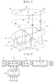
- Fig. 1 is a cross sectional view showing an etalon device in a variable spectroscopic element according to the present embodiment.
- Fig. 2 is a plane view showing the etalon device shown in Fig. 1 .
- Fig. 3 is a schematic view showing operations of a pair of optical substrates and four piezoelectric devices in the etalon device shown in Fig. 1 .
- Fig. 4 is a block diagram showing an operation which is performed by a control unit of the variable spectroscopic element according to the embodiment 1.
- Fig. 5 is a graph showing the response characteristic of the etalon device shown in Fig. 1 , Fig.
- Fig. 5A is a graph showing the response characteristic in the case where a variable spectroscopic element in prior art is controlled
- Fig. 5B is a graph showing the response characteristic in the case where the variable spectroscopic element according to the present embodiment is controlled.
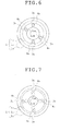
- Fig. 6 is a plane view showing the first example of variations of the etalon device shown in Fig. 1 .
- Fig. 7 is a plane view showing the second example of variations of the etalon device shown in Fig. 1 .
- Fig. 8 is a plane view showing the third example of variations of the etalon device shown in Fig. 1 .
- Fig. 9 is a cross sectional view showing the fourth example of variations of the etalon device shown in Fig. 1 .
- variable spectroscopic element includes an etalon device which is shown in Figs. 1 and 2 and a control unit which is not shown in the drawings.
- this etalon device includes a pair of optical substrates 2, capacitive sensors for measuring a distance between the surfaces of the pair of the optical substrates 2 opposite to each other, and piezoelectric devices which are actuators for moving one substrate of the pair of the optical substrates 2 and the operation of which is controlled by the control unit not shown in the drawings, the pair of the optical substrates 2, the capacitive sensors, and the piezoelectric devices being placed on the inside of an outer frame 1 of the etalon device.
- the outer frame 1 is formed by fitting an annular member 1 2 to one end surface of a cylindrical member 1 1 and fitting an annular member 1 3 to the other end surface of the cylindrical member 1 1 .
- circular openings 1 2 a and 1 3 a are formed in the approximately middle portions of the annular members 1 2 and 1 3 , respectively. And, light passes through the openings 1 2 a and 1 3 a in this etalon device.
- the pair of the optical substrates 2 consists of a fixed substrate 2 1 and a movable substrate 2 2 which are arranged while the surfaces of the optical substrates 2 opposite to each other are being separate from each other and are being parallel to each other.
- the fixed substrate 2 1 is a disk-like optical member which is fixed to the annular member 1 2 of the outer frame 1 on the inside of the outer frame 1 while crossing the axis of light passing through the openings 1 2 a and 1 3 a.
- the movable substrate 2 2 is a disk-like optical member which is held by the piezoelectric devices while crossing light passing through the openings 1 2 a and 1 3 a.
- Such a pair of the optical substrates 2 is formed in such a way that the piezoelectric devices move the movable substrate 2 2 along the axis of light passing through the openings 1 2 a and 1 3 a or along the line connecting the centers of mass of the surfaces of the pair of the optical substrates opposite to each other so that a distance between the surfaces of the optical substrates opposite to each other can be changed.
- a first capacitive sensor 3 1 , a second capacitive sensor 3 2 , a third capacitive sensor 3 3 , and a fourth capacitive sensor 3 4 consist of a pair of electrodes 3 11 and 3 12 , a pair of electrodes 3 21 and 3 22 , a pair of electrodes 3 31 and 3 32 , and a pair of electrodes 3 41 and 3 42 , respectively. And, these pairs of the electrodes are arranged at positions on the surfaces of the pair of the optical substrates 2 opposite to each other at which these electrodes do not intercept light passing through the openings 1 2 a and 1 3 a of the outer frame 1, respectively while the electrodes of each of the pairs of the electrodes are facing each other.
- these capacitive sensors have characteristics in which electrostatic capacities between their electrodes change in inverse proportion to a distance between the surfaces of the optical substrates. And, in this etalon device, values acquired by these capacitive sensors are transformed into values of distances between the surfaces of the optical substrates 2 to be outputted to the control unit which is not shown in the drawings.
- a first piezoelectric device 4 1 , a second piezoelectric device 4 2 , a third piezoelectric device 4 3 , and a fourth piezoelectric device 4 4 are fixed to the annular member 1 3 of the outer frame 1 on the inside of the outer frame 1 in such a way that these piezoelectric devices do not intercept light passing through the openings 1 2 a and 1 3 a.
- the first, second, third, and fourth capacitive sensors 3 1 , 3 2 , 3 3 , and 3 4 and the first, second, third, and fourth piezoelectric devices 4 1 , 4 2 , 4 3 , and 4 4 are arranged at positions at which the first piezoelectric device 4 1 overlaps with the first capacitive sensor 3 1 , the second piezoelectric device 4 2 overlaps with the second capacitive sensor 3 2 , the third piezoelectric device 4 3 overlaps with the third capacitive sensor 3 3 , and the fourth piezoelectric device 4 overlaps with the fourth capacitive sensor 3 4 when these capacitive sensors and these piezoelectric devices are viewed from the direction along the line connecting the centers of mass of the surfaces of the pair of the optical substrates 2 opposite to each other, respectively.
- the first capacitive sensor 3 1 , the third capacitive sensor 3 3 , the first piezoelectric device 4 1 , and the third piezoelectric device 4 3 are arranged at positions at which the first capacitive sensor 3 1 and the first piezoelectric device 4 1 are symmetrical to the third capacitive sensor 3 3 and the third piezoelectric device 4 3 with respect to the line connecting the centers of mass of the surfaces of the pair of the optical substrates 2 opposite to each other when the first and third capacitive sensors and the first and third piezoelectric devices are viewed from the direction along the line connecting the centers of mass of the surfaces of the pair of the optical substrates 2, respectively.
- the second capacitive sensor 3 2 , the fourth capacitive sensor 3 4 , the second piezoelectric device 4 2 , and the fourth piezoelectric device 4 4 are arranged at positions at which the second capacitive sensor 3 2 and the second piezoelectric device 4 2 are symmetrical to the fourth capacitive sensor 3 4 and the fourth piezoelectric device 4 4 with respect to the line connecting the centers of mass of the surfaces of the pair of the optical substrates 2 opposite to each other when the second and fourth capacitive sensors and the second and fourth piezoelectric devices are viewed from the direction along the line connecting the centers of mass of the surfaces of the pair of the optical substrates 2, respectively.
- the first capacitive sensor 3 1 and the first piezoelectric device 4 1 , the second capacitive sensor 3 2 and the second piezoelectric device 4 2 , the third capacitive sensor 3 3 and the third piezoelectric device 4 3 , and the fourth capacitive sensor 3 4 and the fourth piezoelectric device 4 4 are arranged at regular intervals when these capacitive sensors and these piezoelectric devices are viewed from the direction along the line connecting the centers of mass of the surfaces of the pair of the optical substrates 2 opposite to each other.
- etalon devices in the prior art are operated in such a way that: the first piezoelectric device 4 1 is driven on the basis of an output value of the first capacitive sensor 3 1 so that the surface distance at the positions at which the first capacitive sensor 3 1 is placed has the target value of x 0 ; and, similarly, the second piezoelectric device 4 2 is driven on the basis of an output value of the second capacitive sensor 3 2 , the third piezoelectric device 4 3 is driven on the basis of an output value of the third capacitive sensor 3 3 , and the fourth piezoelectric device 4 4 is driven on the basis of an output value of the fourth capacitive sensor 3 4 .
- Another ways of solving it include a way of giving each of the piezoelectric devices a value which is calculated in advance against the interference from another piezoelectric device as a command value.
- a calculation of that command value is very complicated, so that it takes a long time to make the surface distance between the pair of the optical substrates 2 reach the target value of x 0 , similarly.
- variable spectroscopic element in the variable spectroscopic element according to the present embodiment, four output values from the first to fourth capacitive sensors 3 1 , 3 2 , 3 3 , and 3 4 are transformed into three parameters and operations are performed. In such a manner, drive control of the first to fourth piezoelectric devices 4 1 , 4 2 , 4 3 , and 4 4 is performed.
- the target value x 0 of a distance between the center of mass G 1 of the surface of the fixed substrate 2 1 and the center of mass G 2 of the surface of the movable substrate 2 2 , these surfaces being opposite to each other, a target value ⁇ 0 of a first angle made between the surface perpendicular to the line connecting the centers of mass G 1 and G 2 and the surface of the movable substrate 2 2 opposite to the surface perpendicular to the line, and a target value ⁇ 0 of a second angle made between the surface perpendicular to the line connecting the centers of mass G 1 and G 2 and the surface of the movable substrate 2 2 opposite to the surface perpendicular to the line are first inputted into the control unit through a target value input part 5 1 , as shown in Fig.
- a sensor output transformation part 5 2 acquires surface distances x 1 , x 2 , x 3 , and x 4 between the optical substrates at the positions at which the first, second, third, and fourth capacitive sensors 3 1 , 3 2 , 3 3 , and 3 4 are placed respectively, the surface distances x 1 , x 2 , x 3 , and x 4 at the respective positions being measured by these capacitive sensors 3 1 , 3 2 , 3 3 , and 3 4 respectively.
- the sensor output transformation part 5 2 transforms the surface distances x 1 , x 2 , x 3 , and x 4 into the present value x of a distance between the centers of mass G 1 and G 2 , the present value ⁇ of the first angle, and the present value ⁇ of the second angle.
- a difference value calculating part 5 3 calculates a value ex of a difference between the target value x 0 inputted through the target value input part 5 1 and the value x transformed by the sensor output transformation part 5 2 , a value e ⁇ of a difference between the target value ⁇ 0 inputted through the target value input part 5 1 and the value ⁇ transformed by the sensor output transformation part 5 2 , and a value e ⁇ of a difference between the target value ⁇ 0 inputted through the target value input part 5 1 and the value ⁇ transformed by the sensor output transformation part 5 2 .
- a command value calculating part 5 4 carries out PID control on the basis of the difference values ex, e ⁇ , and e ⁇ that are calculated by the difference value calculating part 5 3 , and the command value calculating part 5 4 finds command values x c , ⁇ c , and ⁇ c .
- a command value transformation part 5 5 transforms the command values x c , ⁇ c , and ⁇ c that are found by the command value calculating part 5 4 , into command values x c1 , x c2 , x c3 , and x c4 for the first to fourth piezoelectric devices 4 1 , 4 2 , 4 3 , and 4 4 respectively.
- the command values x c1 , x c2 , x c3 , and x c4 for the first to fourth piezoelectric devices 4 1 , 4 2 , 4 3 , and 4 4 respectively are inputted into a piezoelectric device-driving driver which drives the first, second, third, and fourth piezoelectric devices 4 1 , 4 2 , 4 3 , and 4 4 and which is not shown in the drawings, and a drive voltage is applied to each of the first to fourth piezoelectric devices 4 1 , 4 2 , 4 3 , and 4 4 by this piezoelectric device-driving driver.
- the first to fourth piezoelectric devices 4 1 , 4 2 , 4 3 , and 4 4 are driven by the voltages that are applied by the piezoelectric device-driving driver on the basis of the command values x c1 , x c2 , x c3 , and x c4 respectively, so that the movable substrate 2 2 is moved and the surface distance x between the pair of the optical substrates 2 is changed.
- Fig. 5 is a graph showing experimental results on the response characteristics of etalon devices when feedback control is performed in each of variable spectroscopic elements. Besides, a surface distance between the pair of the optical substrates (nm) is plotted on the vertical axis and time (sec) is plotted on the horizontal axis, and Fig. 5A shows an experimental result in a variable spectroscopic element in the prior art, and Fig. 5B shows an experimental result in the variable spectroscopic element of the present embodiment. Besides, in this experiment, as shown with broken lines, signals are inputted while the target value is being changed every 0.02 seconds.
- variable spectroscopic elements of the present embodiment can change their optical characteristics accurately even though the optical characteristics are changed continuously and at high speed.
- An etalon device shown in Fig. 6 is different from the etalon device of the variable spectroscopic element of the above-described embodiment.
- the first capacitive sensor 3 1 and the first piezoelectric device 4 1 , the second capacitive sensor 3 2 and the second piezoelectric device 4 2 , the third capacitive sensor 3 3 and the third piezoelectric device 4 3 , and the fourth capacitive sensor 3 4 and the fourth piezoelectric device 4 4 are not arranged at regular intervals when these capacitive sensors and these piezoelectric devices are viewed from the direction along the line connecting the centers of mass of the surfaces of the pair of the optical substrates 2 opposite to each other.
- the control unit can control the etalon device shown in Fig. 6 by performing the same operation as is performed in the etalon device of the variable spectroscopic
- Etalon devices shown in Figs. 7 and 8 are different from the etalon device of the variable spectroscopic element of the above-described embodiment.
- the first capacitive sensor 3 1 and the first piezoelectric device 4 1 , the second capacitive sensor 3 2 and the second piezoelectric device 4 2 , the third capacitive sensor 3 3 and the third piezoelectric device 4 3 , and the fourth capacitive sensor 3 4 and the fourth piezoelectric device 4 4 are arranged while the first capacitive sensor 3 1 and the first piezoelectric device 4 1 , the second capacitive sensor 3 2 and the second piezoelectric device 4 2 , the third capacitive sensor 3 3 and the third piezoelectric device 4 3 , and the fourth capacitive sensor 3 4 and the fourth piezoelectric device 4 4 are not overlapping with each other respectively, when these capacitive sensors and these piezoelectric devices are viewed from the direction along the line connecting the centers of mass of
- the control units can control the etalon devices shown in Figs. 7 and 8 by performing the same operation as is performed in the etalon device of the variable spectroscopic element of the above-described embodiment, even though these capacitive sensors and these piezoelectric devices are arranged as shown in Fig. 7 or 8 .
- An etalon device shown in Fig. 9 is different from the etalon device of the variable spectroscopic element of the above-described embodiment.
- the etalon device shown in Fig. 9 does not include the outer frame 1, and the first piezoelectric device 4 1 , the second piezoelectric device 4 2 , the third piezoelectric device 4 3 , and the fourth piezoelectric device 4 4 are fixed on the surface of the fixed substrate 2 1 opposite to the other surface in such a way that the first piezoelectric device 4 1 , the second piezoelectric device 4 2 , the third piezoelectric device 4 3 , and the fourth piezoelectric device 4 4 do not intercept light passing through the etalon device.
- control unit can control the etalon device shown in Fig. 9 by performing the same operation as is performed in the etalon device of the variable spectroscopic element of the above-described embodiment, even though these capacitive sensors and these piezoelectric devices are arranged as shown in Fig. 9 .
- a variable spectroscopic element of the embodiment 2 which is provided with an etalon device of a variable spectroscopic element according to the present invention is explained using Figs. 10 and 11 .
- components constituting the etalon device of the variable spectroscopic element of the present embodiment are the same as those constituting the etalon device of the embodiment 1 respectively. Accordingly, components having the same constitution are given the same reference numeral as in the embodiment 1, and detailed explanations of these components are omitted.
- a constitution of a control unit of the variable spectroscopic element of the present embodiment and operation performed in the control unit for the present embodiment are approximately the same as those for the control unit of the variable spectroscopic element of the embodiment 1. Accordingly, detailed explanations of these matters are omitted.
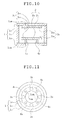
- Fig. 10 is a cross sectional view showing an etalon device in a variable spectroscopic element according to the present embodiment.
- Fig. 11 is a plane view showing the etalon device shown in Fig. 10 .
- An etalon device of the variable spectroscopic element according to the present embodiment is different from the etalon device of the variable spectroscopic element of the embodiment 1.
- the first to fourth piezoelectric devices 4 1 , 4 2 , 4 3 , and 4 4 and the first to fourth capacitive sensors 3 1 , 3 2 , 3 3 , and 3 4 are arranged at regular intervals on a circle while the piezoelectric devices are alternating with the capacitive sensors, when these capacitive sensors and these piezoelectric devices are viewed from the direction along the line connecting the centers of mass of the surfaces of the pair of the optical substrates 2 opposite to each other.
- variable spectroscopic element of the embodiment 1 a distance x between the centers of mass of the surfaces of the pair of the optical substrates 2 opposite to each other is calculated with output values from the first to fourth capacitive sensors 3 1 , 3 2 , 3 3 , and 3 4 , a first angle ⁇ is calculated with output values from the first and third capacitive sensors 3 1 and 3 3 , and a second angle ⁇ is calculated with output values from the second and fourth capacitive sensors 3 2 and 3 4 .
- operations of the first and third piezoelectric devices 4 1 and 4 3 are controlled on the basis of the distance x between the centers of mass of the surfaces and the first angle ⁇
- operations of the second and fourth piezoelectric devices 4 2 and 4 4 are controlled on the basis of the distance x between the centers of mass of the surfaces and the second angle ⁇ .
- variable spectroscopic element of the present embodiment a distance x between the centers of mass of the surfaces of the pair of the optical substrates 2 opposite to each other, a first angle ⁇ , and a second angle ⁇ are calculated with all of output values from the first to fourth capacitive sensors 3 1 , 3 2 , 3 3 , and 3 4 . And, operations of the first to fourth piezoelectric devices 4 1 , 4 2 , 4 3 , and 4 4 are controlled on the basis of the distance x between the centers of mass of the surfaces, the first angle ⁇ , and the second angle ⁇ .
- the capacitive sensors 3 and the piezoelectric devices 4 are not arranged at positions at which the capacitive sensors 3 are overlapping with the piezoelectric devices 4 respectively when these capacitive sensors and these piezoelectric devices are viewed from the direction along the line connecting the centers of mass of the surfaces of the pair of the optical substrates 2 opposite to each other, a distance between the surfaces of the pair of the optical substrates 2 opposite to each other, which is detected by the capacitive sensors 3, is transformed into surface distances x 1 , x 2 , x 3 , and x 4 between the optical substrates at positions at which the first to fourth piezoelectric devices 4 1 , 4 2 , 4 3 , and 4 4 are placed respectively. As a result, it is possible to perform the same control as is performed in the embodiment 1.
- variable spectroscopic elements of the present embodiment can change their optical characteristics accurately even though their optical characteristics are changed continuously and at high speed.
- Variable spectroscopic elements according to the present invention can be favorably used for spectroscopic endoscopes and so on because the variable spectroscopic endoscopes can change their optical characteristics at high speed and accurately. As a result, the variable spectroscopic elements according to the present invention are extremely practically useful.
Landscapes
- Physics & Mathematics (AREA)
- General Physics & Mathematics (AREA)
- Spectroscopy & Molecular Physics (AREA)
- Optics & Photonics (AREA)
- Mechanical Light Control Or Optical Switches (AREA)
- Spectrometry And Color Measurement (AREA)
- Measurement Of Length, Angles, Or The Like Using Electric Or Magnetic Means (AREA)
Applications Claiming Priority (2)
| Application Number | Priority Date | Filing Date | Title |
|---|---|---|---|
| JP2010078213A JP5363393B2 (ja) | 2010-03-30 | 2010-03-30 | 可変分光素子 |
| PCT/JP2011/055995 WO2011122323A1 (ja) | 2010-03-30 | 2011-03-15 | 可変分光素子 |
Publications (1)
| Publication Number | Publication Date |
|---|---|
| EP2555037A1 true EP2555037A1 (en) | 2013-02-06 |
Family
ID=44712044
Family Applications (1)
| Application Number | Title | Priority Date | Filing Date |
|---|---|---|---|
| EP11762563A Withdrawn EP2555037A1 (en) | 2010-03-30 | 2011-03-15 | Variable spectral element |
Country Status (5)
| Country | Link |
|---|---|
| US (1) | US8482737B2 (enExample) |
| EP (1) | EP2555037A1 (enExample) |
| JP (1) | JP5363393B2 (enExample) |
| CN (1) | CN102834760B (enExample) |
| WO (1) | WO2011122323A1 (enExample) |
Cited By (1)
| Publication number | Priority date | Publication date | Assignee | Title |
|---|---|---|---|---|
| EP2804032A1 (fr) * | 2013-05-14 | 2014-11-19 | Compagnie Industrielle des Lasers Cilas | Dispositif optique d'obturation rapide |
Families Citing this family (4)
| Publication number | Priority date | Publication date | Assignee | Title |
|---|---|---|---|---|
| JP5363393B2 (ja) | 2010-03-30 | 2013-12-11 | オリンパス株式会社 | 可変分光素子 |
| JP5363394B2 (ja) * | 2010-03-30 | 2013-12-11 | オリンパス株式会社 | 可変分光素子 |
| JP5530375B2 (ja) | 2011-02-01 | 2014-06-25 | オリンパス株式会社 | 可変分光素子 |
| US8893565B2 (en) * | 2012-07-13 | 2014-11-25 | Nokia Corporation | Apparatus for sensing |
Family Cites Families (9)
| Publication number | Priority date | Publication date | Assignee | Title |
|---|---|---|---|---|
| JPH06241899A (ja) * | 1993-01-29 | 1994-09-02 | Shimadzu Corp | エタロン駆動機構 |
| JP3812550B2 (ja) * | 2003-07-07 | 2006-08-23 | セイコーエプソン株式会社 | 波長可変光フィルタ |
| JP5085101B2 (ja) | 2006-11-17 | 2012-11-28 | オリンパス株式会社 | 可変分光素子 |
| JP2008183350A (ja) * | 2007-01-31 | 2008-08-14 | Olympus Corp | 可変分光素子、分光装置および内視鏡システム |
| JP2008197362A (ja) * | 2007-02-13 | 2008-08-28 | Olympus Corp | 可変分光素子 |
| JP5798709B2 (ja) * | 2009-03-04 | 2015-10-21 | セイコーエプソン株式会社 | 光フィルター及びそれを備えた光モジュール |
| JP2010224011A (ja) * | 2009-03-19 | 2010-10-07 | Olympus Corp | エタロン装置及びそれを備えた光学ユニット |
| JP5363393B2 (ja) | 2010-03-30 | 2013-12-11 | オリンパス株式会社 | 可変分光素子 |
| JP5363394B2 (ja) * | 2010-03-30 | 2013-12-11 | オリンパス株式会社 | 可変分光素子 |
-
2010
- 2010-03-30 JP JP2010078213A patent/JP5363393B2/ja not_active Expired - Fee Related
-
2011
- 2011-03-15 EP EP11762563A patent/EP2555037A1/en not_active Withdrawn
- 2011-03-15 CN CN201180017145.7A patent/CN102834760B/zh not_active Expired - Fee Related
- 2011-03-15 WO PCT/JP2011/055995 patent/WO2011122323A1/ja not_active Ceased
-
2012
- 2012-09-14 US US13/617,425 patent/US8482737B2/en not_active Expired - Fee Related
Non-Patent Citations (1)
| Title |
|---|
| See references of WO2011122323A1 * |
Cited By (2)
| Publication number | Priority date | Publication date | Assignee | Title |
|---|---|---|---|---|
| EP2804032A1 (fr) * | 2013-05-14 | 2014-11-19 | Compagnie Industrielle des Lasers Cilas | Dispositif optique d'obturation rapide |
| FR3005750A1 (fr) * | 2013-05-14 | 2014-11-21 | Cilas | Dispositif optique d'obturation rapide. |
Also Published As
| Publication number | Publication date |
|---|---|
| US8482737B2 (en) | 2013-07-09 |
| CN102834760A (zh) | 2012-12-19 |
| WO2011122323A1 (ja) | 2011-10-06 |
| JP2011209574A (ja) | 2011-10-20 |
| JP5363393B2 (ja) | 2013-12-11 |
| US20130016359A1 (en) | 2013-01-17 |
| CN102834760B (zh) | 2014-11-26 |
Similar Documents
| Publication | Publication Date | Title |
|---|---|---|
| EP2555037A1 (en) | Variable spectral element | |
| EP3232246B1 (en) | Method and device for monitoring movement of mirrors in a mems device | |
| JP2013238755A5 (enExample) | ||
| EP3054580A1 (en) | Optical module | |
| EP2998777A1 (de) | Piezoelektrischer positionssensor für piezoelektrisch angetriebene resonante mikrospiegel | |
| US8848196B2 (en) | Spectrophotometer having prompt spectrophotometric measurement | |
| JP2013092474A5 (enExample) | ||
| US20150270477A1 (en) | Actuator | |
| JP2010145988A (ja) | 可変型回折格子装置 | |
| WO2014155448A1 (ja) | ミラーデバイス | |
| KR102207614B1 (ko) | Mems 미러 스캐너 구동 방법 및 위 방법을 이용한 mems 미러 스캐너 구동 장치 | |
| EP2555038A1 (en) | Variable spectral element | |
| JP2010224011A (ja) | エタロン装置及びそれを備えた光学ユニット | |
| US11060909B2 (en) | Spectrometer, analysis equipment, and wavelength-variable light source | |
| JP5530375B2 (ja) | 可変分光素子 | |
| EP4312071A1 (en) | Image projection device and control method for image projection device | |
| EP4109165A1 (en) | Optical scanning device and control method thereof | |
| Protopopov | Beam alignment and positioning techniques | |
| US11815627B2 (en) | Mirror assembly for light steering with reduced finger thickness | |
| US12345875B2 (en) | Optical scanning device which detects a deflection angle of a mirror unit based on outputs from light detectors | |
| US20210405348A1 (en) | Reduced nonlinearities for resonant deflection of a scanning mirror | |
| US20210405349A1 (en) | Actuation of a scanning mirror using an elastic coupling | |
| Overstolz et al. | Compact And Stress-Released Piston Tip-Tilt Mirror | |
| Chen et al. | Application of twisting algorithm to a 2D electrostatic MEMS micromirror |
Legal Events
| Date | Code | Title | Description |
|---|---|---|---|
| PUAI | Public reference made under article 153(3) epc to a published international application that has entered the european phase |
Free format text: ORIGINAL CODE: 0009012 |
|
| 17P | Request for examination filed |
Effective date: 20120924 |
|
| AK | Designated contracting states |
Kind code of ref document: A1 Designated state(s): AL AT BE BG CH CY CZ DE DK EE ES FI FR GB GR HR HU IE IS IT LI LT LU LV MC MK MT NL NO PL PT RO RS SE SI SK SM TR |
|
| DAX | Request for extension of the european patent (deleted) | ||
| RAP1 | Party data changed (applicant data changed or rights of an application transferred) |
Owner name: OLYMPUS CORPORATION |
|
| RIN1 | Information on inventor provided before grant (corrected) |
Inventor name: WAKAI, HIROSHI |
|
| STAA | Information on the status of an ep patent application or granted ep patent |
Free format text: STATUS: THE APPLICATION HAS BEEN WITHDRAWN |
|
| 18W | Application withdrawn |
Effective date: 20161229 |