WO2011122176A1 - 半導体装置の製造方法、表示装置およびその製造方法 - Google Patents
半導体装置の製造方法、表示装置およびその製造方法 Download PDFInfo
- Publication number
- WO2011122176A1 WO2011122176A1 PCT/JP2011/053819 JP2011053819W WO2011122176A1 WO 2011122176 A1 WO2011122176 A1 WO 2011122176A1 JP 2011053819 W JP2011053819 W JP 2011053819W WO 2011122176 A1 WO2011122176 A1 WO 2011122176A1
- Authority
- WO
- WIPO (PCT)
- Prior art keywords
- film
- channel layer
- manufacturing
- gate insulating
- insulating film
- Prior art date
- Legal status (The legal status is an assumption and is not a legal conclusion. Google has not performed a legal analysis and makes no representation as to the accuracy of the status listed.)
- Ceased
Links
Images



Classifications
-
- H—ELECTRICITY
- H10—SEMICONDUCTOR DEVICES; ELECTRIC SOLID-STATE DEVICES NOT OTHERWISE PROVIDED FOR
- H10D—INORGANIC ELECTRIC SEMICONDUCTOR DEVICES
- H10D30/00—Field-effect transistors [FET]
- H10D30/60—Insulated-gate field-effect transistors [IGFET]
- H10D30/67—Thin-film transistors [TFT]
- H10D30/6729—Thin-film transistors [TFT] characterised by the electrodes
- H10D30/6737—Thin-film transistors [TFT] characterised by the electrodes characterised by the electrode materials
- H10D30/6739—Conductor-insulator-semiconductor electrodes
-
- H—ELECTRICITY
- H10—SEMICONDUCTOR DEVICES; ELECTRIC SOLID-STATE DEVICES NOT OTHERWISE PROVIDED FOR
- H10D—INORGANIC ELECTRIC SEMICONDUCTOR DEVICES
- H10D30/00—Field-effect transistors [FET]
- H10D30/01—Manufacture or treatment
- H10D30/021—Manufacture or treatment of FETs having insulated gates [IGFET]
- H10D30/031—Manufacture or treatment of FETs having insulated gates [IGFET] of thin-film transistors [TFT]
- H10D30/0312—Manufacture or treatment of FETs having insulated gates [IGFET] of thin-film transistors [TFT] characterised by the gate electrodes
- H10D30/0316—Manufacture or treatment of FETs having insulated gates [IGFET] of thin-film transistors [TFT] characterised by the gate electrodes of lateral bottom-gate TFTs comprising only a single gate
-
- H—ELECTRICITY
- H10—SEMICONDUCTOR DEVICES; ELECTRIC SOLID-STATE DEVICES NOT OTHERWISE PROVIDED FOR
- H10D—INORGANIC ELECTRIC SEMICONDUCTOR DEVICES
- H10D30/00—Field-effect transistors [FET]
- H10D30/01—Manufacture or treatment
- H10D30/021—Manufacture or treatment of FETs having insulated gates [IGFET]
- H10D30/031—Manufacture or treatment of FETs having insulated gates [IGFET] of thin-film transistors [TFT]
- H10D30/0321—Manufacture or treatment of FETs having insulated gates [IGFET] of thin-film transistors [TFT] comprising silicon, e.g. amorphous silicon or polysilicon
-
- H—ELECTRICITY
- H10—SEMICONDUCTOR DEVICES; ELECTRIC SOLID-STATE DEVICES NOT OTHERWISE PROVIDED FOR
- H10D—INORGANIC ELECTRIC SEMICONDUCTOR DEVICES
- H10D30/00—Field-effect transistors [FET]
- H10D30/60—Insulated-gate field-effect transistors [IGFET]
- H10D30/67—Thin-film transistors [TFT]
- H10D30/6729—Thin-film transistors [TFT] characterised by the electrodes
- H10D30/673—Thin-film transistors [TFT] characterised by the electrodes characterised by the shapes, relative sizes or dispositions of the gate electrodes
- H10D30/6732—Bottom-gate only TFTs
-
- H—ELECTRICITY
- H10—SEMICONDUCTOR DEVICES; ELECTRIC SOLID-STATE DEVICES NOT OTHERWISE PROVIDED FOR
- H10D—INORGANIC ELECTRIC SEMICONDUCTOR DEVICES
- H10D30/00—Field-effect transistors [FET]
- H10D30/60—Insulated-gate field-effect transistors [IGFET]
- H10D30/67—Thin-film transistors [TFT]
- H10D30/674—Thin-film transistors [TFT] characterised by the active materials
- H10D30/6741—Group IV materials, e.g. germanium or silicon carbide
- H10D30/6743—Silicon
- H10D30/6745—Polycrystalline or microcrystalline silicon
-
- G—PHYSICS
- G02—OPTICS
- G02F—OPTICAL DEVICES OR ARRANGEMENTS FOR THE CONTROL OF LIGHT BY MODIFICATION OF THE OPTICAL PROPERTIES OF THE MEDIA OF THE ELEMENTS INVOLVED THEREIN; NON-LINEAR OPTICS; FREQUENCY-CHANGING OF LIGHT; OPTICAL LOGIC ELEMENTS; OPTICAL ANALOGUE/DIGITAL CONVERTERS
- G02F1/00—Devices or arrangements for the control of the intensity, colour, phase, polarisation or direction of light arriving from an independent light source, e.g. switching, gating or modulating; Non-linear optics
- G02F1/01—Devices or arrangements for the control of the intensity, colour, phase, polarisation or direction of light arriving from an independent light source, e.g. switching, gating or modulating; Non-linear optics for the control of the intensity, phase, polarisation or colour
- G02F1/13—Devices or arrangements for the control of the intensity, colour, phase, polarisation or direction of light arriving from an independent light source, e.g. switching, gating or modulating; Non-linear optics for the control of the intensity, phase, polarisation or colour based on liquid crystals, e.g. single liquid crystal display cells
- G02F1/133—Constructional arrangements; Operation of liquid crystal cells; Circuit arrangements
- G02F1/136—Liquid crystal cells structurally associated with a semi-conducting layer or substrate, e.g. cells forming part of an integrated circuit
- G02F1/1362—Active matrix addressed cells
- G02F1/1368—Active matrix addressed cells in which the switching element is a three-electrode device
Definitions
- the present invention relates to a method of manufacturing a semiconductor device, a display device, and a method of manufacturing the same, and more particularly to a method of manufacturing a semiconductor device that reduces off-current, a display device including such a semiconductor device, and a method of manufacturing the same.
- an active matrix liquid crystal display device has been provided with a thin film transistor (hereinafter referred to as “TFT”) having a channel layer made of an amorphous silicon film as a switching element of a pixel formation portion.
- TFT thin film transistor
- liquid crystal display devices have been developed with higher definition, and accordingly, TFTs are also required to have low on-resistance in order to shorten the charge time of the pixel capacitance of the pixel formation portion. It was.
- a microcrystalline silicon film having a higher mobility has been used instead of an amorphous silicon film as a channel layer of a TFT.
- the microcrystalline silicon film contains not only microcrystalline components but also amorphous components. Therefore, crystallinity mismatch occurs at the interface between the microcrystalline component and the amorphous component in the microcrystalline silicon film, and dangling bonds are formed.
- the dangling bonds cause a drain current (hereinafter referred to as “off current” or “leakage current”) that flows between the source electrode and the drain electrode when the TFT is in an off state.
- off current a drain current
- dangling bonds contained in the microcrystalline silicon film are terminated with hydrogen ions or hydrogen radicals, and the off-current flowing through the TFT is reduced.
- Japanese Unexamined Patent Application Publication No. 2008-124111 discloses a TFT manufacturing method in which the surface of a channel layer made of a polycrystalline silicon film is exposed to plasma generated by applying high-frequency power to a gas containing oxygen or a gas containing nitrogen. Is described. As a result, the dangling bonds present on the surface of the channel layer are terminated, so that the off-current of the TFT is reduced.
- the dangling bonds that cause off-current generation are not only formed in the microcrystalline silicon film serving as the channel layer, but also formed in the silicon nitride film used as the gate insulating film.
- the channel layer is a microcrystalline silicon film
- the silicon nitride film serving as the gate insulating film is an amorphous film.
- the channel layer is also an amorphous silicon film, since both are amorphous films, dangling bonds existing on the surface of the silicon nitride film are terminated by dangling bonds of the amorphous silicon film. As a result, the number of dangling bonds on the surface of the silicon nitride film is reduced, so that the off current is reduced.
- the channel layer is a microcrystalline silicon film
- crystallinity mismatch occurs at the interface between the microcrystalline silicon film and the silicon nitride film, so that the dangling bonds existing on the surface of the silicon nitride film are microcrystalline silicon. It becomes difficult to be terminated by dangling bonds existing on the surface of the film. As a result, there is a problem that many dangling bonds remain on the surface of the silicon nitride film, and an off-current caused by the remaining dangling bonds flows.
- the ohmic contact layer formed between the channel layer of the TFT and the source electrode and the drain electrode is also a microcrystalline silicon film, the dangling bonds remain in the ohmic contact layer without being terminated. ing. For this reason, unless the dangling bonds remaining in the ohmic contact layer are terminated, there is a problem that an off-current caused by the dangling bonds in the ohmic contact layer flows.
- Japanese Unexamined Patent Application Publication No. 2008-124111 describes that a dangling bond existing on the surface of a polycrystalline silicon film serving as a channel layer is terminated. However, the termination of dangling bonds existing in the surface of the gate insulating film or in the ohmic contact layer is not described. For this reason, it is not possible to reduce the off-current due to the dangling bonds existing in the surface of the gate insulating film or in the ohmic contact layer.
- an object of the present invention is to provide a method for manufacturing a semiconductor device that reduces off-current.
- a method for manufacturing a semiconductor device comprising a gate insulating film including an amorphous nitride semiconductor film, Ions generated from a gas containing nitrogen, or dangling bonds existing on the surface of either the gate insulating film in which the channel layer is to be formed or the channel layer in which the gate insulating film is to be formed, It includes a first termination step that terminates with a radical.
- the ions or radicals generated from the nitrogen-containing gas are contained in plasma generated by applying high-frequency power to the nitrogen-containing gas, or in a gas obtained by heating the nitrogen-containing gas to a predetermined temperature. It is an ion or a radical.
- the first termination step includes Forming a gate insulating film on the insulating substrate so as to cover the gate electrode; and A first plasma processing step of exposing the surface of the gate insulating film to plasma generated by applying high-frequency power to the nitrogen-containing gas; A channel layer forming step of forming a channel layer on the gate insulating film processed by the first plasma processing step.
- the first termination step includes Forming a gate insulating film on the insulating substrate so as to cover the gate electrode; and A first gas treatment step of exposing the surface of the gate insulating film to a gas obtained by heating the gas containing nitrogen to a predetermined temperature; A channel layer forming step of forming a channel layer on the gate insulating film processed by the first gas processing step.
- the method further includes an ohmic contact layer forming step of patterning the impurity-doped crystalline semiconductor film to form ohmic contact layers on both ends of the channel layer, respectively.
- the first termination step includes A channel layer forming step of forming the channel layer on the insulating substrate; A third plasma treatment step of exposing the surface of the channel layer to plasma generated by applying high-frequency power to the nitrogen-containing gas; A gate insulating film forming step of forming the gate insulating film on an upper surface of the channel layer processed by the third plasma processing step; And a gate electrode forming step of forming the gate electrode on the gate insulating film.
- the first termination step includes A channel layer forming step of forming the channel layer on the insulating substrate; A third gas treatment step of exposing the surface of the channel layer to a gas obtained by heating the gas containing nitrogen to a predetermined temperature; A gate insulating film forming step of forming the gate insulating film on an upper surface of the channel layer processed by the third gas processing step; And a gate electrode forming step of forming the gate electrode on the gate insulating film.
- the gas containing nitrogen is ammonia gas.
- the crystalline semiconductor film is a microcrystalline silicon film;
- the gate insulating film is an amorphous silicon nitride film.
- the crystalline semiconductor film is a microcrystalline silicon film;
- the gate insulating film is an amorphous silicon oxynitride film.
- a twelfth aspect of the present invention is the fifth or sixth aspect of the present invention.
- the crystalline semiconductor film doped with impurities is a microcrystalline silicon film doped with impurities.
- a thirteenth aspect of the present invention is a display device including a plurality of semiconductor devices on an insulating substrate, A display device, wherein the semiconductor device is manufactured by a method for manufacturing a semiconductor device according to any one of the first to twelfth aspects of the present invention.
- a fourteenth aspect of the present invention is a method for manufacturing a display device comprising a plurality of semiconductor devices on an insulating substrate,
- the method for manufacturing the display device includes a step of manufacturing the semiconductor device by the method for manufacturing a semiconductor device according to any one of the first to twelfth aspects of the present invention.
- a dangling bond existing on the surface of the gate insulating film where the channel layer is to be formed or a dangling bond existing on the surface of the channel layer where the gate insulating film is to be formed is provided. Is terminated by ions or radicals generated from a gas containing nitrogen. This reduces the number of dangling bonds on their surface. After that, even if a channel layer is formed on the surface of the gate insulating film in which the dangling bond is terminated or a gate insulating film is formed on the surface of the channel layer in which the dangling bond is terminated, the crystallinity mismatch The number of unbonded hands due to the increase hardly increases. For this reason, the off-current flowing through the semiconductor device can be reduced.
- plasma generated by applying high-frequency power to a gas containing nitrogen as ions or radicals that terminate dangling bonds or a gas containing nitrogen is heated to a predetermined temperature. Ions and radicals contained in the generated gas. Thereby, the termination
- the surface of the gate insulating film is changed to a gas containing nitrogen. It is exposed to plasma generated by applying high frequency power. At this time, the dangling bonds existing on the surface of the gate insulating film are terminated by ions or radicals contained in the plasma, so that dangling bonds are reduced. Even when a channel layer including a crystalline semiconductor film is formed over the gate insulating film, the number of dangling bonds due to mismatch in crystallinity between the gate insulating film and the channel layer is hardly increased. Accordingly, off current flowing in the semiconductor device can be reduced.
- the surface of the gate insulating film is heated to a predetermined temperature after forming the gate insulating film including the amorphous nitride semiconductor film and before forming the channel layer. Exposed to nitrogen-containing gas. At this time, dangling bonds existing on the surface of the gate insulating film are terminated by ions or radicals contained in the gas heated to a predetermined temperature. Accordingly, off current flowing in the semiconductor device can be reduced.
- the crystalline semiconductor film doped with impurities is formed so as to cover the channel layer.
- the crystalline semiconductor film doped with impurities is exposed to plasma generated by applying high-frequency power to a gas containing nitrogen.
- dangling bonds existing at the crystal grain boundaries of the crystalline semiconductor film doped with impurities are terminated by ions or radicals contained in the plasma.
- the number of dangling bonds present at the crystal grain boundaries of the crystalline semiconductor film doped with impurities is reduced, so that the off-current flowing through the semiconductor device can be further reduced.
- the crystalline semiconductor film doped with impurities is formed so as to cover the channel layer.
- the crystalline semiconductor film doped with impurities is exposed to a gas containing nitrogen heated to a predetermined temperature.
- dangling bonds present at the crystal grain boundaries of the crystalline semiconductor film doped with impurities are terminated by ions or radicals contained in the gas heated to a predetermined temperature.
- the number of dangling bonds present at the crystal grain boundaries of the crystalline semiconductor film doped with impurities is reduced, so that the off-current flowing through the semiconductor device can be further reduced.
- the surface of the channel is It is exposed to plasma generated by applying high-frequency power to a gas containing gas.
- the dangling bonds existing on the surface of the channel layer are terminated by ions or radicals contained in the plasma, the number of dangling bonds decreases.
- the number of dangling bonds due to the crystallinity mismatch between the channel layer and the gate insulating film hardly increases. Accordingly, off current flowing in the semiconductor device can be reduced.
- the surface of the channel is Exposure to gas heated to the temperature of At this time, since the dangling bonds existing on the surface of the channel layer are terminated by ions or radicals heated to a predetermined temperature, the number of dangling bonds decreases. Further, even when a gate insulating film is formed over the channel layer, the number of dangling bonds due to the crystallinity mismatch between the channel layer and the gate insulating film hardly increases. Accordingly, off current flowing in the semiconductor device can be reduced.
- the gas containing nitrogen is ammonia gas. For this reason, it is easy to generate ions or radicals that terminate dangling bonds by applying high-frequency power or heating. Therefore, the termination of the dangling hand can be efficiently performed, so that the off-current flowing through the semiconductor device can be easily reduced.
- the crystalline semiconductor film is a microcrystalline silicon film
- the gate insulating film is an amorphous silicon nitride film.
- the crystalline semiconductor film is a microcrystalline silicon film
- the gate insulating film is an amorphous silicon oxynitride film. Also in this case, the same effect as that of the tenth aspect of the present invention is achieved.
- the crystalline semiconductor film doped with impurities is a microcrystalline silicon film
- the off-current is reduced in the semiconductor device manufactured by the manufacturing method according to any one of the first to twelfth aspects of the present invention. If the switching element of the display device is formed using such a semiconductor device, the image signal accumulated in the pixel capacitance of each pixel formation portion can be held for a long time. Thereby, the display device can display a high-quality image. In addition, by forming a display device drive circuit using a semiconductor device, the display device can manufacture a display device with low power consumption.
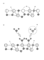
- FIG. 1 is a schematic diagram which shows the surface of the silicon nitride film 1 before performing ammonia plasma processing
- (b) is a schematic diagram which shows the surface of the silicon nitride film 1 after performing ammonia plasma processing.
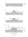
- (A)-(d) is process sectional drawing which shows each manufacturing process of TFT shown in FIG. (E) to (g) are process cross-sectional views illustrating each manufacturing process of the TFT shown in FIG.
- FIG. (H) to (j) are process cross-sectional views showing respective manufacturing processes of the TFT shown in FIG. (A)-(d) is process sectional drawing which shows each manufacturing process of the top gate type TFT concerning 2nd Embodiment.
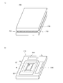
- (A) is a figure which shows the structure of the liquid crystal panel contained in an active matrix type liquid crystal display device
- (b) is a figure which shows the structure of the TFT substrate contained in the liquid crystal panel shown in (a).
- FIG. 1 is a cross-sectional view showing a configuration of a bottom gate type TFT 10 used for basic examination.
- the configuration of the TFT 10 will be described with reference to FIG.
- a gate electrode 20 is formed on a glass substrate 15 which is an insulating substrate.
- a gate insulating film 30 made of a silicon nitride film (SiNx) is formed so as to cover the entire glass substrate 15 including the gate electrode 20.
- the film thickness of the gate insulating film 30 is, for example, 350 nm.
- An island-shaped channel layer 40 is formed on the surface of the gate insulating film 30 so as to extend left and right across the gate electrode 20 in plan view.
- the film thickness of the channel layer 40 is 15 nm, for example.
- the channel layer 40 is made of an intrinsic microcrystalline silicon film that does not contain impurities.
- An etching stopper layer 50 made of a silicon nitride film is formed at the center of the surface of the channel layer 40.
- An ohmic contact layer 60a extending from the upper left surface of the etching stopper layer 50 to the left end portion of the channel layer 40, and an ohmic contact extending so as to cover from the upper right surface of the etching stopper layer 50 to the right end portion of the channel layer 40 Layer 60b is formed. Since the TFT 10 is an n-channel type, these ohmic contact layers 60a and 60b are made of a microcrystalline silicon film (hereinafter referred to as “n + silicon film”) doped with an n-type impurity at a high concentration, and an etching stopper layer 50. It is separated on the upper surface of the left and right.
- the ohmic contact layer 60a functions as a source region, and the ohmic contact layer 60b functions as a drain region.
- a source electrode 70a extending from the right end portion on the ohmic contact layer 60a to the gate insulating film 30 so as to cover the ohmic contact layer 60a, and a gate insulating film 30 covering the ohmic contact layer 60b from the left end portion on the ohmic contact layer 60b.
- a drain electrode 70b extending upward is formed.
- the source electrode 70a is connected so as to be in ohmic contact with the channel layer 40 via the ohmic contact layer 60a
- the drain electrode 70b is connected so as to be in ohmic contact with the channel layer 40 via the ohmic contact layer 60b.
- a protective film 80 made of a silicon nitride film is formed so as to cover the entire glass substrate 15 including the source electrode 70a and the drain electrode 70b.
- the off current was measured using the TFT 10.
- the off-current measurement is performed after the formation of the silicon nitride film to be the gate insulating film 30 and before the formation of the microcrystalline silicon film to be the channel layer 40 on the surface of the gate insulating film 30 by ammonia plasma treatment or ammonia. It performed about TFT10 which performed the flow process.
- the ammonia plasma treatment refers to a treatment in which high-frequency power is applied to ammonia gas supplied to the chamber to generate plasma, and the surface of the silicon nitride film is exposed to the generated plasma.
- the ammonia plasma treatment was performed under the following condition (1).
- Condition (1) Gas used: Ammonia (flow rate: 70 sccm) Degree of vacuum in chamber: 200 Pa Insulating substrate temperature: 250 ° C High frequency power supply output power: 60W Processing time: 15 sec
- the ammonia flow process is a process in which the ammonia gas supplied to the chamber is heated and the surface of the silicon nitride film is exposed to the heated ammonia gas.
- the ammonia flow treatment was performed under the condition (2) shown below.
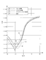
- FIG. 2 is a diagram showing the Vg-Id characteristics of the TFT 10.
- FIG. 2 shows the Vg-Id characteristics of the TFT 10 manufactured under the following four conditions.
- A When ammonia flow treatment is performed
- B When ammonia plasma treatment is performed
- C In
- B when n + silicon film is further subjected to ammonia flow treatment
- D Ammonia flow treatment is also performed by ammonia plasma When no treatment was applied (conventional conditions)
- the TFT 10 Since the TFT 10 is an n-channel type, the TFT 10 is turned off when a negative voltage is applied to the gate electrode 20. However, a slight off current flows between the source electrode 70a and the drain electrode 70b at this time. As shown in FIG. 2, the current value of the off current becomes the smallest when a voltage of about ⁇ 10 V is applied to the gate electrode 20 in any case. However, the minimum value of the current that flows when a voltage of about ⁇ 10 V is applied is different. Therefore, the cases (A) to (C) are evaluated based on the case (D). In the case of (D), the current value of the off-current decreases only to about 1 ⁇ 10 ⁇ 12 A.
- the minimum current value of the off current is reduced to about 5 ⁇ 10 ⁇ 13 A.
- the minimum current value of the off current further decreases to about 3 ⁇ 10 ⁇ 14 A. From these results, it was found that the off-current can be reduced by applying ammonia flow treatment or ammonia plasma treatment to the surface of the silicon nitride film. Further, comparing the ammonia plasma treatment and the ammonia flow treatment, it was found that the ammonia plasma treatment can further reduce the off-current. From this, it is considered that the ammonia plasma treatment is easier to terminate dangling bonds existing on the surface of the silicon nitride film than the ammonia flow treatment. In FIG.
- FIG. 3A is a schematic diagram showing the surface of the silicon nitride film before the ammonia plasma treatment is performed
- FIG. 3B is a schematic diagram showing the surface of the silicon nitride film after the ammonia plasma treatment is performed. It is. As shown in FIG. 3A, the silicon atoms 31 existing in the silicon nitride film are bonded to the adjacent silicon atoms 31 via the nitrogen atoms 32 or directly bonded.
- the plasma generated from the ammonia gas contains a lot of NH 2 ions 35. Therefore, as shown in FIG. 3B, when the surface of the silicon nitride film, which is an amorphous film, is exposed to plasma, NH 2 ions 35 contained in the plasma are unbonded on the surface of the silicon nitride film. Since it joins with the hand 33 and terminates the unjoined hand 33, the number of the unjoined hand 33 decreases. After that, even when a microcrystalline silicon film serving as a channel layer is formed, the number of dangling bonds due to the crystallinity mismatch between the silicon nitride film and the channel layer is hardly increased. Thereby, the off-current flowing through the TFT 10 can be reduced.
- the plasma generated from the ammonia gas contains not only NH 2 ions but also H radicals, NH radicals, NH ions, etc., and these radicals or ions also exist on the surface of the silicon nitride film.
- the joint 33 is terminated.
- the ammonia gas in the chamber is heated to 220 to 250 ° C., whereby the bond between the nitrogen atom and the hydrogen atom (NH bond) in the ammonia molecule is broken or excited by thermal energy. Or As a result, ions such as NH 2 ions and radicals such as H radicals and NH radicals are generated. Therefore, by exposing the surface of the silicon nitride film to heated ammonia gas, these ions or radicals are bonded to the dangling bonds 33 existing on the surface of the silicon nitride film, and many dangling bonds 33 are terminated. To do. Note that the ratio of N—H bonds cut by heating depends on the heating temperature. For example, at 220 to 250 ° C., if the ratio of N—H bonds to be cut is estimated, It is about 1/1000.
- the amorphous silicon film is a film formed by plasma enhanced chemical vapor deposition (CVD) and has a thickness of 25 nm.
- the ammonia plasma treatment was performed under the following condition (3).
- Condition (3) Gas used: Ammonia (flow rate: 100 sccm) Degree of vacuum in chamber: 200 Pa Insulating substrate temperature: 250 ° C High frequency power output: 60W Processing time: 60 sec
- the ammonia flow treatment was performed under the following condition (4).
- FIG. 4 is a diagram showing the refractive index of an amorphous silicon film subjected to ammonia plasma treatment or ammonia flow treatment. Note that the refractive index of the amorphous silicon film was measured by ellipsometry.
- the refractive index when the amorphous silicon film is not subjected to any treatment is 4.225.
- the refractive index of the amorphous silicon film subjected to ammonia plasma treatment is 4.206
- the refractive index of the amorphous silicon film subjected to ammonia flow treatment is 4.217.
- the refractive index when the ammonia plasma treatment is performed is smaller. From this, it can be seen that the ammonia plasma treatment terminates more dangling bonds of the amorphous silicon film than the ammonia flow treatment.
- the surface of the silicon nitride film that becomes the gate insulating film 30 is subjected to ammonia plasma treatment shown in the condition (1), and then a microcrystalline silicon film that becomes the channel layer 40 is formed. Further, a case where an ammonia flow process is performed after forming an n + silicon film to be ohmic contact layers 60a and 60b on the microcrystalline silicon film will be described.
- the ammonia flow treatment was performed under the following condition (5).
- the off current of the TFT 10 subjected to such processing is as shown in FIG. 2C, and the minimum current value is about 1 ⁇ 10 ⁇ 13 A. From this, it was found that the off-current decreases as in the cases of (A) and (B). Thus, in order to reduce the off-current of the TFT, it is effective to perform the ammonia flow treatment not only on the surface of the gate insulating film but also on the n + silicon film that becomes the ohmic contact layers 60a and 60b. all right. Moreover, it turned out that the same result can be obtained even if ammonia plasma treatment is performed instead of ammonia flow treatment.
- TFT manufacturing method> A method for manufacturing the bottom gate TFT 10 according to the first embodiment of the present invention will be described.
- a TFT that functions as a switching element provided in each pixel formation portion of the display panel will be described as an example, and the manufacturing method will be described.
- the present invention is not limited to this, and can also be applied to the manufacture of TFTs constituting a drive circuit provided around the display panel of a liquid crystal display device.
- a metal film (not shown) having a thickness of, for example, 100 to 500 nm and containing titanium (Ti) as a main component is formed on the glass substrate 15 by sputtering.
- a metal film mainly composed of Ti a metal film mainly composed of tungsten (W), molybdenum (Mo), aluminum (Al) or the like, or a metal film made of an alloy thereof is formed. Also good.
- a resist pattern (not shown) is formed on the surface of the metal film using a photolithography method. As shown in FIG. 5A, the metal film is etched by wet etching using the resist pattern as a mask to form the gate electrode 20. Thereafter, the resist pattern is peeled off. Note that the gate electrode 20 may be formed by using a dry etching method instead of the wet etching method.
- a silicon nitride film to be the gate insulating film 30 is formed by plasma CVD so as to cover the entire glass substrate 15 including the gate electrode 20.
- the thickness of the silicon nitride film is, for example, 200 to 500 nm, and preferably 350 nm.
- a silicon nitride film is formed under the following conditions.
- Deposition source gas Monosilane (SiH 4 ) (flow rate 10 sccm) Nitrogen (N 2 ) (flow rate 100 sccm) Ammonia (NH 3 ) (flow rate 70 sccm) Dilution gas: Hydrogen (H 2 ) (flow rate 200 sccm) Insulating substrate temperature: 250 ° C Degree of vacuum in chamber: 200 Pa High-frequency power output: 125W
- the surface of the silicon nitride film is subjected to ammonia plasma treatment. Since the conditions of the ammonia plasma treatment are the same as the condition (1) used in the basic study, the description thereof is omitted.
- ammonia flow treatment may be performed instead of ammonia plasma treatment. Since the conditions of the ammonia flow treatment are the same as the condition (2) used in the basic study, the description thereof is omitted.
- a microcrystalline silicon film 41 is formed on the surface of the gate insulating film 30.
- the microcrystalline silicon film 41 is formed using a high-density plasma CVD apparatus such as an ICP (Inductively Coupled Plasma) method or a surface wave plasma method.
- the microcrystalline silicon film 41 is formed under the conditions that the temperature of the insulating substrate is 300 ° C., the degree of vacuum in the chamber is 110 Pa, the output of the high frequency power source is 250 W, and the flow rates of monosilane gas and hydrogen gas are 30 sccm and 3000 sccm, respectively.
- the film thickness of the microcrystalline silicon film 41 formed in this manner is 10 to 20 nm, preferably 15 nm.
- a silicon nitride film 51 is formed on the surface of the microcrystalline silicon film 41 using a plasma CVD method.
- the film formation conditions for the silicon nitride film 51 are the same except for the film formation conditions for the gate insulating film 30 and the film thickness.
- the film thickness of the silicon nitride film 51 is, for example, 150 nm.
- a resist pattern 55 is formed on the surface of the silicon nitride film 51 by a photolithography method at a position facing the gate electrode 20 with the microcrystalline silicon film 41 interposed therebetween.
- the silicon nitride film 51 is etched by plasma etching using the resist pattern 55 as a mask. As a result, an etching stopper layer 50 is formed at the center of the surface of the microcrystalline silicon film 41. Thereafter, the resist pattern 55 is peeled off.
- n.sup. + Made of microcrystalline silicon and containing, for example, n-type impurities at a high concentration is formed by high-density plasma CVD so as to cover the entire glass substrate 15 including the etching stopper layer 50.
- a silicon film 61 is formed.
- the film thickness of the n + silicon film 61 is 30 to 50 nm, preferably 35 nm.
- phosphine (PH 3 ) gas is used to dope n-type impurities.
- ammonia flow process to the n + silicon film 61. Since the conditions for the ammonia flow treatment are the same as the conditions (5) used in the basic study, the description thereof is omitted. Instead of performing an ammonia flow process on the n + silicon film 61, an ammonia plasma process may be performed.
- a resist pattern (not shown) is formed on the surface of the n + silicon film 61 using a photolithography technique. Using the resist pattern as a mask, n + silicon film 61 and microcrystalline silicon film 41 are successively etched by dry etching. Thereby, the n + silicon layer 62 and the channel layer 40 are formed. Thereafter, the resist pattern is peeled off. Next, a source metal film 71 is formed by sputtering so as to cover the entire glass substrate 15 including the n + silicon layer 62.
- the source metal film 71 is, for example, a metal film having a thickness of 50 to 200 nm and containing titanium.
- a resist pattern 75 having an opening above the etching stopper layer 50 is formed on the surface of the source metal film 71 using a photolithography method.
- the source metal film 71 is etched by a wet etching method using the resist pattern 75 as a mask to form a source electrode 70a and a drain electrode 70b. Note that the source metal film 71 may be etched by plasma etching instead of wet etching.
- the n + silicon layer 62 is etched by plasma etching to form two ohmic contact layers 60 a and 60 b separated on the upper and lower sides of the etching stopper layer 50. Since the etching stopper layer 50 made of silicon nitride is formed on the upper surface of the channel layer 40, the etching of the n + silicon film 61 is stopped by the etching stopper layer 50, and the channel layer 40 is not etched. .
- the ohmic contact layer 60a formed in this way extends so as to cover from the upper left end of the etching stopper layer 50 to the left end of the channel layer 40, and the ohmic contact layer 60b extends from the upper right end of the etching stopper layer 50.
- the channel layer 40 extends to cover the right end portion.
- a protective film 80 made of silicon nitride is formed so as to cover the entire glass substrate 15 including the source electrode 70a and the drain electrode 70b.
- the protective film 80 is formed by a plasma CVD method using a source gas containing monosilane gas and ammonia gas, and the film thickness is, for example, 200 nm.
- the TFT 10 is manufactured through the series of manufacturing processes described above.
- the dangling bonds present on the surface of the silicon nitride film are NH 2 contained in the heated ammonia gas. Terminated by ions such as ions or radicals such as NH radicals. Thereby, the off-current of the TFT 10 can be reduced as in the case where the ammonia plasma treatment is performed.
- the gate insulating film 30 but also the n + silicon film 61 to be the ohmic contact layers 60 a and 60 b are present at the crystal grain boundaries of the n + silicon film 61 by performing ammonia plasma treatment or ammonia flow treatment. Unbound hands are terminated. Thereby, the off current of the TFT 10 can be further reduced.
- Ammonia gas is likely to generate ions and radicals that terminate dangling bonds by applying high-frequency power or heating. Thereby, the termination of the dangling bonds existing on the gate insulating film 30 can be performed efficiently, so that the off-current flowing through the TFT 10 can be easily reduced.
- Second Embodiment> A method for manufacturing the top gate type TFT 110 according to the second embodiment of the present invention will be described. Similar to the TFT 10 according to the first embodiment, the TFT 110 functions as a switching element provided in each pixel formation portion of the display panel as an example, and a manufacturing method thereof will be described. However, the present invention is not limited to this, and can also be applied to the manufacture of TFTs constituting a drive circuit provided around the display panel of a liquid crystal display device.
- FIG. 8A to FIG. 8D are process cross-sectional views showing each manufacturing process of the TFT 110.
- the base insulating film 120 is formed on the glass substrate 115.
- the base insulating film 120 is a stacked insulating film in which a silicon oxide film is stacked on the upper surface of a silicon nitride film.
- a microcrystalline silicon film 131 is formed so as to cover the base insulating film 120. Similar to the microcrystalline silicon film 41 of the first embodiment, the microcrystalline silicon film 131 is formed by using a high-density plasma CVD apparatus.
- an ammonia flow process is performed on the surface of the microcrystalline silicon film 131.
- the ammonia flow treatment is performed under the following conditions. Gas used: Ammonia (flow rate: 100 sccm) Temperature in the chamber: 220-250 ° C Degree of vacuum in chamber: 145 Pa Processing time: 180 sec
- the microcrystalline silicon film 131 is patterned by a photolithography method to form an island-shaped channel layer 130.
- a silicon nitride film 141 is formed by plasma CVD so as to cover the entire glass substrate 115 including the channel layer.
- a gate electrode 150 is formed by patterning a refractory metal film (not shown) such as titanium formed on the silicon nitride film 141 by photolithography.
- the silicon nitride film 141 is etched using the gate electrode 150 as a mask to form a gate insulating film 140 sandwiched between the gate electrode 150 and the channel layer 130.
- the channel layer 130 is doped with an n-type impurity by ion implantation or the like.
- regions doped with n-type impurities become a source region 130a and a drain region 130b, respectively, and a region sandwiched between the source region 130a and the drain region 130b becomes a channel region 130c.
- an interlayer insulating film 160 is formed so as to cover the entire glass substrate 115, and contact holes 170 reaching the source region 130a and the drain region 130b are opened in the interlayer insulating film 160, respectively.
- a source electrode 180a and a drain electrode 180b made of a refractory metal such as titanium and electrically connected to the source region 130a and the drain region 130b through the contact hole 170 are formed.
- a protective film (not shown) is formed so as to cover the entire glass substrate 115.
- the silicon nitride film 141 formed on the upper surface of the channel layer 130 obtained by etching the microcrystalline silicon film 131 is an amorphous film.
- the silicon nitride film 141 is formed on the top surface of the microcrystalline silicon film 131, many unbonded hands existing on the surface of the microcrystalline silicon film 131 remain without being terminated. Therefore, after the microcrystalline silicon film 131 is formed and before the silicon nitride film 141 is formed, the surface of the microcrystalline silicon film 131 is subjected to an ammonia flow process to nitride the surface of the microcrystalline silicon film 131.
- the manufacturing method of the TFT 110 even if ammonia plasma treatment is performed instead of performing ammonia flow treatment on the surface of the microcrystalline silicon film 131, dangling bonds existing on the surface of the microcrystalline silicon film 131 are terminated. , The off-state current of the TFT 110 can be reduced.
- the gate insulating films 30 and 140 in the first and second embodiments have been described as being silicon nitride films.
- the gate insulating films 30 and 140 are not limited to the silicon nitride film, but may be any insulating film containing nitrogen and silicon, such as a silicon oxynitride film (SiON). Good.
- the off current of the TFTs 10 and 110 can be reduced by performing the above-described ammonia plasma treatment or ammonia flow treatment on the surface of the insulating film.
- the channel layers 40 and 130 of the first and second embodiments have been described as being formed of a microcrystalline silicon film.
- the channel layers 40 and 130 may be formed of a polycrystalline silicon film.
- the polycrystalline silicon film is also a crystalline silicon film, many dangling bonds are formed on the surface of the silicon nitride film that is an amorphous film. Therefore, before the polycrystalline silicon film is formed, the surface of the silicon nitride film is subjected to the above-described ammonia plasma treatment or ammonia flow treatment to reduce the number of dangling bonds on the silicon nitride film, and then the polycrystalline silicon film. When a film is formed, the off current of the TFT 10 can be reduced.
- the present invention can be applied to a crystalline silicon film including not only a microcrystalline silicon film but also a polycrystalline silicon film.
- the semiconductor material constituting the channel layers 40 and 130 and the ohmic contact layers 60a and 60b of the first and second embodiments is silicon.
- the channel layers 40 and 130 and the ohmic contact layers 60a and 60b may be formed of a semiconductor material such as germanium silicon.
- the TFTs 10 and 110 manufactured by the manufacturing method described in each of the above embodiments can reduce off-current. Therefore, a configuration of a liquid crystal display device using such TFTs 10 and 110 will be described.
- FIG. 9A is a diagram illustrating a configuration of a liquid crystal panel 200 included in the active matrix liquid crystal display device
- FIG. 9B is a diagram illustrating a TFT substrate 210 included in the liquid crystal panel 200 illustrated in FIG. FIG.
- the liquid crystal panel 200 includes two glass substrates disposed to face each other so as to sandwich the liquid crystal layer, and a liquid crystal layer (not shown) sandwiched between the two glass substrates. And a sealing material 230 that seals the liquid crystal layer.
- a glass substrate in which a plurality of pixel forming portions including TFTs are formed in a matrix is called a TFT substrate 210, which is disposed to face the TFT substrate 210, and a color filter or the like is formed.
- the glass substrate is referred to as a CF substrate 220.
- the TFT substrate 210 includes a plurality of pixel forming portions 221.
- FIG. 9B shows only one pixel formation portion 221 for convenience, but a plurality of pixel formation portions 221 are formed in a matrix on the TFT substrate 210.
- a TFT functioning as the switching element 222 and a pixel electrode 223 connected to the switching element 222 are formed in the pixel formation portion 221.
- a gate driver 240 and a source driver 250 are provided in the frame area outside the pixel formation portion 221.
- the gate driver 240 outputs a control signal for controlling the timing for turning on / off the switching element 222 to the gate wiring GL, and the source driver 250 outputs an image signal for displaying an image on the pixel forming unit 221 and an image signal.
- a control signal for controlling is output to the source line SL.
- the image signal applied to the source wiring SL is connected to the pixel electrode via the switching element 222. 223.
- the pixel electrode 223 forms a pixel capacitance together with a common electrode (not shown) formed on the CF substrate 220 and holds a given image signal.
- the backlight corresponding to the image signal is transmitted through the pixel forming unit 221 and the image is displayed on the liquid crystal panel 200.
- the contact resistance of the TFTs 10 and 110 is small, so that the current flowing through the switching elements 222 can be increased.
- the switching element 222 can charge the image capacitance given from the source wiring SL to the pixel capacitor in a short time, and therefore, the number of the pixel formation portions 221 is increased to increase the definition of the liquid crystal panel 200. Is possible.
- the gate driver 240 and the source driver 250 are formed on the TFT substrate 210 using continuous grain boundary crystal silicon (Continuous Grain silicon), if the gate driver 240 and the source driver 250 are configured using the TFTs 10 and 110, The operating speed of the gate driver 240 and the source driver 250 can be increased. As a result, the circuit scale of the gate driver 240 and the source driver 250 is reduced, so that the frame of the liquid crystal panel 200 can be reduced and the power consumption of the liquid crystal display device can be reduced.
- continuous grain boundary crystal silicon Continuous Grain silicon
- the TFT 10 according to the first embodiment or the TFT 110 according to the second embodiment can also be used for a display device such as an organic EL (Electroluminescence) display device or a plasma display device.
- a display device such as an organic EL (Electroluminescence) display device or a plasma display device.
- the present invention is suitable for a display device such as an active matrix liquid crystal display device, and particularly suitable for a switching element formed in the pixel formation portion or a transistor of a drive circuit for driving the pixel formation portion. .
Landscapes
- Thin Film Transistor (AREA)
Abstract
ガラス基板上にゲート絶縁膜となる窒化シリコン膜を成膜した後であって、チャネル層となる微結晶シリコン膜を成膜する前の窒化シリコン膜の表面には、シリコン原子(31)の未結合手(33)が存在する。そこで、窒化シリコン膜の表面にアンモニアプラズマ処理を施す。その結果、窒化シリコン膜の表面の未結合手(33)は、プラズマ中に含まれるNH2イオン(35)などのイオンまたはNHラジカルなどのラジカルによって終端される。これにより、その後に微結晶シリコン膜を成膜しても、ゲート絶縁膜とチャネル層との結晶性の不整合に起因する未結合手の数はほとんど増加せず、TFTに流れるオフ電流を低減することができる。
Description
本発明は、半導体装置の製造方法、表示装置およびその製造方法に関し、特に、オフ電流を低減する半導体装置の製造方法、そのような半導体装置を含む表示装置およびその製造方法に関する。
従来、アクティブマトリクス型液晶表示装置には、画素形成部のスイッチング素子として、非晶質シリコン膜からなるチャネル層を備えた薄膜トランジスタ(Thin Film Transistor:以下、「TFT」と略す)が設けられていた。しかし、近年、液晶表示装置の高精細化が進展し、それに伴ってTFTでも、画素形成部の画素容量の充電時間を短くするために、オン抵抗を小さくすることが要求されるようになってきた。このような要求に対応するため、TFTのチャネル層として、非晶質シリコン膜の代わりに、移動度がより大きな微結晶シリコン膜が用いられるようになってきた。
微結晶シリコン膜は、微結晶成分だけでなく非晶質成分も含む。このため、微結晶シリコン膜内の微結晶成分と非晶質成分との界面で結晶性の不整合が生じ、未結合手(dangling bond)が形成される。未結合手は、TFTがオフ状態の時にソース電極とドレイン電極との間に流れるドレイン電流(以下、「オフ電流」または「リーク電流」という)を発生させる原因になる。そこで、微結晶シリコン膜を水素プラズマに晒すことによって、微結晶シリコン膜内に含まれる未結合手を水素イオンや水素ラジカルで終端し、TFTに流れるオフ電流を低減していた。
日本の特開2008-124111号公報には、多結晶シリコン膜からなるチャネル層の表面を、酸素を含むガス、または窒素を含むガスに高周波電力を印加して生成したプラズマに晒すTFTの製造方法が記載されている。これにより、チャネル層の表面に存在する未結合手が終端されるので、TFTのオフ電流は低減される。
しかし、オフ電流の発生原因となる未結合手は、チャネル層となる微結晶シリコン膜内に形成されているだけではなく、ゲート絶縁膜として用いられる窒化シリコン膜にも形成されている。特に、チャネル層が微結晶シリコン膜である場合には、窒化シリコン膜の表面に多くの未結合手が存在する。これは次の理由によると考えられる。ゲート絶縁膜となる窒化シリコン膜は非晶質膜である。チャネル層も非晶質シリコン膜である場合には、いずれも非晶質膜なので、窒化シリコン膜の表面に存在する未結合手は非晶質シリコン膜の未結合手によって終端される。この結果、窒化シリコン膜の表面の未結合手は減少するので、オフ電流は低減される。
しかしながら、チャネル層が微結晶シリコン膜である場合、微結晶シリコン膜と窒化シリコン膜との界面で結晶性の不整合が生じるので、窒化シリコン膜の表面に存在する未結合手は、微結晶シリコン膜の表面に存在する未結合手によって終端されにくくなる。この結果、窒化シリコン膜の表面に多くの未結合手が残り、残った未結合手に起因するオフ電流が流れるという問題がある。
また、TFTのチャネル層と、ソース電極およびドレイン電極との間にそれぞれ形成されるオーミックコンタクト層も微結晶シリコン膜である場合には、オーミックコンタクト層内にも未結合手が終端されずに残っている。このため、オーミックコンタクト層内に残っている未結合手を終端しなければ、オーミックコンタクト層内の未結合手に起因するオフ電流が流れるという問題もある。
日本の特開2008-124111号公報には、チャネル層となる多結晶シリコン膜の表面に存在する未結合手を終端することが記載されている。しかし、ゲート絶縁膜の表面や、オーミックコンタクト層内に存在する未結合手を終端することは記載されていない。このため、ゲート絶縁膜の表面や、オーミックコンタクト層内に存在する未結合手に起因するオフ電流を低減することはできない。
そこで、本発明は、オフ電流を低減する半導体装置の製造方法を提供することを目的とする。
本発明の第1の局面は、絶縁基板上に、結晶性半導体膜からなる島状のチャネル層と、前記チャネル層の導電性を制御するためのゲート電極と、前記ゲート電極と前記チャネル層との間に設けられ、非晶質窒化半導体膜を含むゲート絶縁膜とを備えた半導体装置の製造方法であって、
前記チャネル層が形成されるべき前記ゲート絶縁膜、または、前記ゲート絶縁膜が形成されるべき前記チャネル層のいずれかの表面に存在する未結合手を、窒素を含むガスから生成されたイオンまたはラジカルによって終端する第1の終端工程を含むことを特徴とする。
前記チャネル層が形成されるべき前記ゲート絶縁膜、または、前記ゲート絶縁膜が形成されるべき前記チャネル層のいずれかの表面に存在する未結合手を、窒素を含むガスから生成されたイオンまたはラジカルによって終端する第1の終端工程を含むことを特徴とする。
本発明の第2の局面は、本発明の第1の局面において、
前記窒素を含むガスから生成されたイオンまたはラジカルは、前記窒素を含むガスに高周波電力を印加することにより生成したプラズマ、または、前記窒素を含むガスを所定の温度に加熱したガスに含まれる、イオンまたはラジカルであることを特徴とする。
前記窒素を含むガスから生成されたイオンまたはラジカルは、前記窒素を含むガスに高周波電力を印加することにより生成したプラズマ、または、前記窒素を含むガスを所定の温度に加熱したガスに含まれる、イオンまたはラジカルであることを特徴とする。
本発明の第3の局面は、本発明の第1の局面において、
前記第1の終端工程は、
前記絶縁基板上に、前記ゲート電極を覆うように前記ゲート絶縁膜を形成するゲート絶縁膜形成工程と、
前記ゲート絶縁膜の表面を、前記窒素を含むガスに高周波電力を印加することにより生成したプラズマに晒す第1のプラズマ処理工程と、
前記第1のプラズマ処理工程によって処理された前記ゲート絶縁膜上にチャネル層を形成するチャネル層形成工程とを含むことを特徴とする。
前記第1の終端工程は、
前記絶縁基板上に、前記ゲート電極を覆うように前記ゲート絶縁膜を形成するゲート絶縁膜形成工程と、
前記ゲート絶縁膜の表面を、前記窒素を含むガスに高周波電力を印加することにより生成したプラズマに晒す第1のプラズマ処理工程と、
前記第1のプラズマ処理工程によって処理された前記ゲート絶縁膜上にチャネル層を形成するチャネル層形成工程とを含むことを特徴とする。
本発明の第4の局面は、本発明の第1の局面において、
前記第1の終端工程は、
前記絶縁基板上に、前記ゲート電極を覆うように前記ゲート絶縁膜を形成するゲート絶縁膜形成工程と、
前記ゲート絶縁膜の表面を、前記窒素を含むガスを所定の温度に加熱したガスに晒す第1のガス処理工程と、
前記第1のガス処理工程によって処理された前記ゲート絶縁膜上にチャネル層を形成するチャネル層形成工程とを含むことを特徴とする。
前記第1の終端工程は、
前記絶縁基板上に、前記ゲート電極を覆うように前記ゲート絶縁膜を形成するゲート絶縁膜形成工程と、
前記ゲート絶縁膜の表面を、前記窒素を含むガスを所定の温度に加熱したガスに晒す第1のガス処理工程と、
前記第1のガス処理工程によって処理された前記ゲート絶縁膜上にチャネル層を形成するチャネル層形成工程とを含むことを特徴とする。
本発明の第5の局面は、本発明の第3または第4の局面において、
前記チャネル層を覆うように、不純物をドープされた結晶性半導体膜を形成する半導体膜形成工程と、
前記不純物をドープされた結晶性半導体層の表面を、前記窒素を含むガスに高周波電力を印加することにより生成したプラズマに晒す第2のプラズマ処理工程と
前記第2のプラズマ処理工程によって処理された前記不純物をドープされた結晶性半導体膜をパターニングして、前記チャネル層の両端部上にオーミックコンタクト層をそれぞれ形成するオーミックコンタクト層形成工程とをさらに含むことを特徴とする。
前記チャネル層を覆うように、不純物をドープされた結晶性半導体膜を形成する半導体膜形成工程と、
前記不純物をドープされた結晶性半導体層の表面を、前記窒素を含むガスに高周波電力を印加することにより生成したプラズマに晒す第2のプラズマ処理工程と
前記第2のプラズマ処理工程によって処理された前記不純物をドープされた結晶性半導体膜をパターニングして、前記チャネル層の両端部上にオーミックコンタクト層をそれぞれ形成するオーミックコンタクト層形成工程とをさらに含むことを特徴とする。
本発明の第6の局面は、本発明の第3または第4の局面において、
前記チャネル層を覆うように、不純物をドープされた結晶性半導体膜を形成する半導体膜形成工程と、
前記不純物をドープされた結晶性半導体層の表面を、前記窒素を含むガスを所定の温度に加熱したガスに晒す第2のガス処理工程と、
前記第2のガス処理工程によって処理された前記不純物をドープされた結晶性半導体膜をパターニングして、前記チャネル層の両端部上にオーミックコンタクト層をそれぞれ形成するオーミックコンタクト層形成工程とをさらに含むことを特徴とする。
前記チャネル層を覆うように、不純物をドープされた結晶性半導体膜を形成する半導体膜形成工程と、
前記不純物をドープされた結晶性半導体層の表面を、前記窒素を含むガスを所定の温度に加熱したガスに晒す第2のガス処理工程と、
前記第2のガス処理工程によって処理された前記不純物をドープされた結晶性半導体膜をパターニングして、前記チャネル層の両端部上にオーミックコンタクト層をそれぞれ形成するオーミックコンタクト層形成工程とをさらに含むことを特徴とする。
本発明の第7の局面は、本発明の第1の局面において、
前記第1の終端工程は、
前記絶縁基板上に、前記チャネル層を形成するチャネル層形成工程と、
前記チャネル層の表面を、前記窒素を含むガスに高周波電力を印加することにより生成したプラズマに晒す第3のプラズマ処理工程と、
前記第3のプラズマ処理工程によって処理された前記チャネル層の上面に前記ゲート絶縁膜を形成するゲート絶縁膜形成工程と、
前記ゲート絶縁膜上に前記ゲート電極を形成するゲート電極形成工程とを含むことを特徴とする。
前記第1の終端工程は、
前記絶縁基板上に、前記チャネル層を形成するチャネル層形成工程と、
前記チャネル層の表面を、前記窒素を含むガスに高周波電力を印加することにより生成したプラズマに晒す第3のプラズマ処理工程と、
前記第3のプラズマ処理工程によって処理された前記チャネル層の上面に前記ゲート絶縁膜を形成するゲート絶縁膜形成工程と、
前記ゲート絶縁膜上に前記ゲート電極を形成するゲート電極形成工程とを含むことを特徴とする。
本発明の第8の局面は、本発明の第1の局面において、
前記第1の終端工程は、
前記絶縁基板上に、前記チャネル層を形成するチャネル層形成工程と、
前記チャネル層の表面を、前記窒素を含むガスを所定の温度に加熱したガスに晒す第3のガス処理工程と、
前記第3のガス処理工程によって処理された前記チャネル層の上面に前記ゲート絶縁膜を形成するゲート絶縁膜形成工程と、
前記ゲート絶縁膜上に前記ゲート電極を形成するゲート電極形成工程とを含むことを特徴とする。
前記第1の終端工程は、
前記絶縁基板上に、前記チャネル層を形成するチャネル層形成工程と、
前記チャネル層の表面を、前記窒素を含むガスを所定の温度に加熱したガスに晒す第3のガス処理工程と、
前記第3のガス処理工程によって処理された前記チャネル層の上面に前記ゲート絶縁膜を形成するゲート絶縁膜形成工程と、
前記ゲート絶縁膜上に前記ゲート電極を形成するゲート電極形成工程とを含むことを特徴とする。
本発明の第9の局面は、本発明の第1の局面において、
前記窒素を含むガスはアンモニアガスであることを特徴とする。
前記窒素を含むガスはアンモニアガスであることを特徴とする。
本発明の第10の局面は、本発明の第1の局面において、
前記結晶性半導体膜は微結晶シリコン膜であり、
前記ゲート絶縁膜は非晶質窒化シリコン膜であることを特徴とする。
前記結晶性半導体膜は微結晶シリコン膜であり、
前記ゲート絶縁膜は非晶質窒化シリコン膜であることを特徴とする。
本発明の第11の局面は、本発明の第1の局面において、
前記結晶性半導体膜は微結晶シリコン膜であり、
前記ゲート絶縁膜は非晶質酸窒化シリコン膜であることを特徴とする。
前記結晶性半導体膜は微結晶シリコン膜であり、
前記ゲート絶縁膜は非晶質酸窒化シリコン膜であることを特徴とする。
本発明の第12の局面は、本発明の第5または第6の局面において、
前記不純物をドープされた結晶性半導体膜は、不純物をドープされた微結晶シリコン膜であることを特徴とする。
前記不純物をドープされた結晶性半導体膜は、不純物をドープされた微結晶シリコン膜であることを特徴とする。
本発明の第13の局面は、絶縁基板上に複数の半導体装置を備えた表示装置であって、
前記半導体装置は、本発明の第1から第12のいずれかの局面に係る半導体装置の製造方法によって製造されたことを特徴とする、表示装置。
前記半導体装置は、本発明の第1から第12のいずれかの局面に係る半導体装置の製造方法によって製造されたことを特徴とする、表示装置。
本発明の第14の局面は、絶縁基板上に複数の半導体装置を備えた表示装置の製造方法であって、
前記表示装置の製造方法は、本発明の第1から第12のいずれかの局面に係る半導体装置の製造方法によって前記半導体装置を製造する工程を含むことを特徴とする。
前記表示装置の製造方法は、本発明の第1から第12のいずれかの局面に係る半導体装置の製造方法によって前記半導体装置を製造する工程を含むことを特徴とする。
本発明の第1の局面によれば、チャネル層が形成されるべきゲート絶縁膜の表面に存在する未結合手、または、ゲート絶縁膜が形成されるべきチャネル層の表面に存在する未結合手は、窒素を含むガスから生成されたイオンまたはラジカルによって終端される。これにより、それらの表面の未結合手が減少する。その後、未結合手が終端されたゲート絶縁膜の表面にチャネル層を形成したり、未結合手が終端されたチャネル層の表面にゲート絶縁膜を形成したりしても、結晶性の不整合に起因する未結合手の数はほとんど増加しない。このため、半導体装置に流れるオフ電流を低減することができる。
本発明の第2の局面によれば、未結合手を終端するイオンやラジカルとして、窒素を含むガスに高周波電力を印加することにより生成したプラズマ、または、窒素を含むガスを所定の温度に加熱したガスに含まれるイオンやラジカルを利用する。これにより、未結合手の終端を効率よく行なうことができる。
本発明の第3の局面によれば、非晶質窒化半導体膜を含むゲート絶縁膜を形成した後であって、チャネル層を形成する前に、ゲート絶縁膜の表面を、窒素を含むガスに高周波電力を印加することにより生成したプラズマに晒す。このとき、ゲート絶縁膜の表面に存在する未結合手は、プラズマに含まれるイオンまたはラジカルによって終端されるので、未結合手は減少する。ゲート絶縁膜上に結晶性半導体膜を含むチャネル層を形成しても、ゲート絶縁膜とチャネル層との結晶性の不整合に起因する未結合手の数はほとんど増加しない。これにより、半導体装置に流れるオフ電流を低減することができる。
本発明の第4の局面によれば、非晶質窒化半導体膜を含むゲート絶縁膜を形成した後であって、チャネル層を形成する前に、ゲート絶縁膜の表面を、所定の温度に加熱した窒素を含むガスに晒す。このとき、ゲート絶縁膜の表面に存在する未結合手は、所定の温度に加熱されたガスに含まれるイオンまたはラジカルによって終端される。これにより、半導体装置に流れるオフ電流を低減することができる。
本発明の第5の局面によれば、チャネル層を覆うように、不純物をドープされた結晶性半導体膜を形成する。次に、不純物をドープされた結晶性半導体膜を、窒素を含むガスに高周波電力を印加することにより生成したプラズマに晒す。このとき、不純物をドープされた結晶性半導体膜の結晶粒界に存在する未結合手は、プラズマに含まれるイオンまたはラジカルによって終端される。これにより、不純物をドープされた結晶性半導体膜の結晶粒界に存在する未結合手は減少するので、半導体装置に流れるオフ電流をさらに低減することができる。
本発明の第6の局面によれば、チャネル層を覆うように不純物をドープされた結晶性半導体膜を形成する。次に、不純物をドープされた結晶性半導体膜を、所定の温度に加熱した窒素を含むガスに晒す。このとき、不純物をドープされた結晶性半導体膜の結晶粒界に存在する未結合手は、所定の温度に加熱されたガスに含まれるイオンまたはラジカルによって終端される。これにより、不純物をドープされた結晶性半導体膜の結晶粒界に存在する未結合手は減少するので、半導体装置に流れるオフ電流をさらに低減することができる。
本発明の第7の局面によれば、結晶性半導体膜を含むチャネル層を形成した後であって、非晶質窒化半導体膜を含むゲート絶縁膜を形成する前に、チャネルの表面を、窒素を含むガスに高周波電力を印加することにより生成したプラズマに晒す。このとき、チャネル層の表面に存在する未結合手は、プラズマに含まれるイオンまたはラジカルによって終端されるので、未結合手の数は減少する。さらに、チャネル層上にゲート絶縁膜を形成しても、チャネル層とゲート絶縁膜との結晶性の不整合に起因する未結合手の数はほとんど増加しない。これにより、半導体装置に流れるオフ電流を低減することができる。
本発明の第8の局面によれば、結晶性半導体膜を含むチャネル層を形成した後であって、非晶質窒化半導体膜を含むゲート絶縁膜を形成する前に、チャネルの表面を、所定の温度に加熱されたガスに晒す。このとき、チャネル層の表面に存在する未結合手は、所定の温度に加熱されたイオンまたはラジカルによって終端されるので、未結合手の数は減少する。さらに、チャネル層上にゲート絶縁膜を形成しても、チャネル層とゲート絶縁膜との結晶性の不整合に起因する未結合手の数はほとんど増加しない。これにより、半導体装置に流れるオフ電流を低減することができる。
本発明の第9の局面によれば、窒素を含むガスはアンモニアガスである。このため、高周波電力を印加したり、加熱したりすることにより、未結合手を終端するイオンやラジカルを生成しやすい。したがって、未結合手の終端を効率的に行なうことができるので、半導体装置に流れるオフ電流を容易に低減することができる。
本発明の第10の局面によれば、結晶性半導体膜は微結晶シリコン膜であり、ゲート絶縁膜は非晶質窒化シリコン膜である。この場合、窒素を含むイオンまたはラジカルによってその表面に存在する未結合手を効率的に終端することができる。これにより、半導体装置に流れるオフ電流を容易に低減することができる。
本発明の第11の局面によれば、結晶性半導体膜は微結晶シリコン膜であり、ゲート絶縁膜は非晶質酸窒化シリコン膜である。この場合も、本発明の第10の局面と同様の効果を奏する。
本発明の第12の局面によれば、不純物をドープされた結晶性半導体膜は微結晶シリコン膜であるので、窒素を含むイオンまたはラジカルによって、結晶性半導体膜の結晶粒界に存在する未結合手を効率的に終端することができる。これにより、半導体装置に流れるオフ電流を容易に低減することができる。
本発明の第13の局面によれば、本発明の第1から第12のいずれかの局面に係る製造方法によって製造された半導体装置では、オフ電流が低減される。このような半導体装置を用いて表示装置のスイッチング素子を形成すれば、各画素形成部の画素容量に蓄積された画像信号を長時間保持することができる。これにより、表示装置は高品位の画像を表示することができる。また、半導体装置を用いて表示装置の駆動回路を形成することにより、表示装置は低消費電力の表示装置を製造することができる。
本発明の第14の局面によれば、本発明の第14の局面と同様の効果を奏する。
<1.基礎検討>
<1.1 TFTの構成>
基礎検討に使用したTFT10の構成を説明する。図1は、基礎検討に使用したボトムゲート型TFT10の構成を示す断面図である。図1を参照して、TFT10の構成を説明する。絶縁基板であるガラス基板15上に、ゲート電極20が形成されている。ゲート電極20を含むガラス基板15の全体を覆うように、窒化シリコン膜(SiNx)からなるゲート絶縁膜30が形成されている。ゲート絶縁膜30の膜厚は、例えば350nmである。
<1.1 TFTの構成>
基礎検討に使用したTFT10の構成を説明する。図1は、基礎検討に使用したボトムゲート型TFT10の構成を示す断面図である。図1を参照して、TFT10の構成を説明する。絶縁基板であるガラス基板15上に、ゲート電極20が形成されている。ゲート電極20を含むガラス基板15の全体を覆うように、窒化シリコン膜(SiNx)からなるゲート絶縁膜30が形成されている。ゲート絶縁膜30の膜厚は、例えば350nmである。
ゲート絶縁膜30の表面に、平面視においてゲート電極20を跨いで左右に延びる島状のチャネル層40が形成されている。チャネル層40の膜厚は、例えば15nmである。チャネル層40は、不純物を含まない真性の微結晶シリコン膜からなる。
チャネル層40の表面の中央に、窒化シリコン膜からなるエッチングストッパ層50が形成されている。エッチングストッパ層50の左端上面からチャネル層40の左端部まで覆うように延在するオーミックコンタクト層60aと、エッチングストッパ層50の右端上面からチャネル層40の右端部まで覆うように延在するオーミックコンタクト層60bが形成されている。TFT10はnチャネル型であるので、これらのオーミックコンタクト層60a,60bは、n型不純物を高濃度にドープした微結晶シリコン膜(以下、「n+シリコン膜」という)からなり、エッチングストッパ層50の上面で左右に分離されている。オーミックコンタクト層60aはソース領域として機能し、オーミックコンタクト層60bはドレイン領域として機能する。
オーミックコンタクト層60a上の右端部からオーミックコンタクト層60aを覆ってゲート絶縁膜30上まで延在するソース電極70aと、オーミックコンタクト層60b上の左端部からオーミックコンタクト層60bを覆ってゲート絶縁膜30上まで延在するドレイン電極70bとが形成されている。ソース電極70aはオーミックコンタクト層60aを介してチャネル層40とオーミック接触するように接続され、ドレイン電極70bはオーミックコンタクト層60bを介してチャネル層40とオーミック接触するように接続されている。さらに、ソース電極70aとドレイン電極70bを含むガラス基板15の全体を覆うように、窒化シリコン膜からなる保護膜80が形成されている。
<1.2 検討内容>
上記TFT10を用いてオフ電流を測定した。オフ電流の測定は、ゲート絶縁膜30となる窒化シリコン膜の成膜後であって、チャネル層40となる微結晶シリコン膜の成膜前に、ゲート絶縁膜30の表面にアンモニアプラズマ処理またはアンモニアフロー処理を施したTFT10について行なった。
上記TFT10を用いてオフ電流を測定した。オフ電流の測定は、ゲート絶縁膜30となる窒化シリコン膜の成膜後であって、チャネル層40となる微結晶シリコン膜の成膜前に、ゲート絶縁膜30の表面にアンモニアプラズマ処理またはアンモニアフロー処理を施したTFT10について行なった。
ここで、アンモニアプラズマ処理とは、チャンバに供給されたアンモニアガスに高周波電力を印加してプラズマを生成し、窒化シリコン膜の表面を生成したプラズマに晒す処理をいう。アンモニアプラズマ処理は以下に示す条件(1)により行なった。
条件(1)
使用するガス : アンモニア(流量:70sccm)
チャンバ内の真空度 : 200Pa
絶縁基板温度 : 250℃
高周波電源の出力電力 : 60W
処理時間 : 15sec
条件(1)
使用するガス : アンモニア(流量:70sccm)
チャンバ内の真空度 : 200Pa
絶縁基板温度 : 250℃
高周波電源の出力電力 : 60W
処理時間 : 15sec
アンモニアフロー処理とは、チャンバに供給されたアンモニアガスを加熱し、窒化シリコン膜の表面を加熱したアンモニアガスに晒す処理をいう。アンモニアフロー処理は以下に示す条件(2)により行なった。
条件(2)
使用するガス : アンモニア(流量:70sccm)
チャンバ内の温度 : 220~250℃
チャンバ内の真空度 : 200Pa
処理時間 : 180sec
条件(2)
使用するガス : アンモニア(流量:70sccm)
チャンバ内の温度 : 220~250℃
チャンバ内の真空度 : 200Pa
処理時間 : 180sec
窒化シリコン膜の成膜後、微結晶シリコン膜の成膜前に、窒化シリコン膜の表面にアンモニアプラズマ処理またはアンモニアフロー処理を施したTFT10について、Vg-Id特性(ゲート電圧-ドレイン電流特性)を測定した。図2は、TFT10のVgーId特性を示す図である。図2には、次の4つの条件で製造したTFT10のVg-Id特性が記載されている。
(A)アンモニアフロー処理を施した場合
(B)アンモニアプラズマ処理を施した場合
(C)(B)において、さらにn+シリコン膜にアンモニアフロー処理を施した場合
(D)アンモニアフロー処理もアンモニアプラズマ処理も施さなかった場合(従来条件)
(A)アンモニアフロー処理を施した場合
(B)アンモニアプラズマ処理を施した場合
(C)(B)において、さらにn+シリコン膜にアンモニアフロー処理を施した場合
(D)アンモニアフロー処理もアンモニアプラズマ処理も施さなかった場合(従来条件)
TFT10はnチャネル型であるため、ゲート電極20に負電圧が印加されたときに、TFT10はオフ状態になる。しかし、このときソース電極70aとドレイン電極70bとの間にわずかなオフ電流が流れる。このオフ電流の電流値は、図2に示すように、いずれの場合もゲート電極20に約-10Vの電圧が印加されたときに、最も小さくなる。しかし、約-10Vの電圧を印加したときに流れる電流の最小値はそれぞれ異なる。そこで、(D)の場合を基準にして、(A)~(C)の場合を評価する。(D)の場合は、オフ電流の電流値は約1×10-12Aまでしか低下しない。
しかし、(A)の場合には、オフ電流の最小電流値は約5×10-13A程度にまで低下する。(B)の場合には、オフ電流の最小電流値はさらに低下して、約3×10-14A程度になる。これらの結果から、窒化シリコン膜の表面にアンモニアフロー処理またはアンモニアプラズマ処理を施せば、オフ電流を低減できることがわかった。また、アンモニアプラズマ処理とアンモニアフロー処理とを比較すると、アンモニアプラズマ処理の方が、オフ電流をより低減できることがわかった。このことから、アンモニアプラズマ処理は、アンモニアフロー処理よりも、窒化シリコン膜の表面に存在する未結合手を終端しやすいと考えられる。なお、図2において、(C)の場合は、窒化シリコン膜の表面にアンモニアプラズマ処理を施すとともに、さらにn+シリコン膜(オーミックコンタクト層60a、60b)の表面にもアンモニアフロー処理を施した場合である。この場合も、(B)の場合のように、オフ電流が低下するが、その詳細は後述する。
上述のように、窒化シリコン膜の表面にアンモニアプラズマ処理またはアンモニアフロー処理を施すことにより、TFT10のオフ電流を低減することができる理由を次のように考える。図3(a)は、アンモニアプラズマ処理を施す前の窒化シリコン膜の表面を示す模式図であり、図3(b)は、アンモニアプラズマ処理を施した後の窒化シリコン膜の表面を示す模式図である。図3(a)に示すように、窒化シリコン膜に存在するシリコン原子31は、隣接するシリコン原子31と、窒素原子32を介して結合したり、直接結合したりしている。しかし、窒化シリコン膜の表面には、窒素原子32や他のシリコン原子31と結合していないシリコン原子31の未結合手33が存在する。このような窒化シリコン膜をゲート絶縁膜30とするTFT10では、ゲート絶縁膜30の表面に存在する未結合手33を介してオフ電流が流れる。
アンモニアガスから生成されたプラズマには、NH2イオン35が多く含まれている。そこで、図3(b)に示すように、非晶質膜である窒化シリコン膜の表面をプラズマに晒せば、プラズマ中に含まれるNH2イオン35が、窒化シリコン膜の表面に存在する未結合手33と結合し、未結合手33を終端するので、未結合手33の数が減少する。その後、チャネル層となる微結晶シリコン膜を形成しても、窒化シリコン膜とチャネル層との結晶性の不整合に起因する未結合手の数はほとんど増加しない。これにより、TFT10に流れるオフ電流を低減することができる。
なお、アンモニアガスから生成されたプラズマには、NH2イオンだけでなく、Hラジカル、NHラジカル、NHイオンなどが含まれており、それらのラジカルまたはイオンによっても窒化シリコン膜の表面に存在する未結合手33は終端される。
また、アンモニアフロー処理では、チャンバ内のアンモニアガスを220~250℃に加熱することにより、アンモニア分子内の窒素原子と水素原子との結合(N-H結合)が熱エネルギーによって切断されたり、励起されたりする。この結果、NH2イオンなどのイオンや、HラジカルおよびNHラジカルなどのラジカルが生成される。したがって、窒化シリコン膜の表面を、加熱されたアンモニアガスに晒すことにより、これらのイオンまたはラジカルが、窒化シリコン膜の表面に存在する未結合手33と結合し、多くの未結合手33を終端する。なお、加熱によって切断されるN-H結合の割合は、加熱温度に依存し、例えば220~250℃では、切断されるN-H結合の割合を概算すれば、全N-H結合数の約1/1000程度である。
次に、非晶質シリコン膜に、アンモニアプラズマ処理を施した場合、またはアンモニアフロー処理を施した場合について説明する。非晶質シリコン膜はプラズマCVD(Plasma Enhanced Chemical Vapor Deposition)法によって成膜された膜で、その膜厚は25nmとする。アンモニアプラズマ処理は以下に示す条件(3)により行なった。
条件(3)
使用するガス : アンモニア(流量:100sccm)
チャンバ内の真空度 : 200Pa
絶縁基板温度 : 250℃
高周波電源の出力 : 60W
処理時間 : 60sec
条件(3)
使用するガス : アンモニア(流量:100sccm)
チャンバ内の真空度 : 200Pa
絶縁基板温度 : 250℃
高周波電源の出力 : 60W
処理時間 : 60sec
また、アンモニアフロー処理は以下に示す条件(4)により行なった。
条件(4)
使用するガス : アンモニア(流量:100sccm)
チャンバ内の温度 : 220~250℃
チャンバ内の真空度 : 200Pa
処理時間 : 180sec
条件(4)
使用するガス : アンモニア(流量:100sccm)
チャンバ内の温度 : 220~250℃
チャンバ内の真空度 : 200Pa
処理時間 : 180sec
図4は、アンモニアプラズマ処理またはアンモニアフロー処理を施した非晶質シリコン膜の屈折率を示す図である。なお、非晶質シリコン膜の屈折率は、エリプソメトリ法によって測定した。
図4に示すように、非晶質シリコン膜に何も処理を施していない場合(従来条件)の屈折率は4.225である。これに対して、アンモニアプラズマ処理を施した非晶質シリコン膜の屈折率は4.206であり、アンモニアフロー処理を施した非晶質シリコン膜の屈折率は4.217である。非晶質シリコン膜にアンモニアプラズマ処理またはアンモニアフロー処理を施すことにより、アンモニアプラズマ処理もアンモニアフロー処理も施さない場合に比べて、非晶質シリコン膜の屈折率を小さくすることができる。非晶質シリコン膜の屈折率が小さくなったのは、以下の理由によると考えられる。終端されずに残っていた未結合手、または、未結合手を終端していた水素イオンおよびラジカルがアンモニアガスなどに含まれる水素イオンまたはラジカルなどと反応して水素ガスになって抜けていくことによって発生した未結合手が、非晶質シリコン膜の表面に存在する。これらの未結合手に、NH2イオンやNHイオンなどが結合し、非晶質シリコン膜の表面が窒化されたためと考えられる。このように、非晶質シリコン膜にアンモニアプラズマ処理またはアンモニアフロー処理を施せば、非晶質シリコン膜に存在する未結合手を終端することができる。また、アンモニアプラズマ処理を施した場合とアンモニアフロー処理を施した場合とを比較すると、アンモニアプラズマ処理を施した場合の屈折率がより小さくなっている。このことから、アンモニアプラズマ処理の方が、アンモニアフロー処理よりも、非晶質シリコン膜の未結合手をより多く終端することがわかる。
次に、TFT10において、ゲート絶縁膜30となる窒化シリコン膜の表面に条件(1)に示すアンモニアプラズマ処理を施した後に、チャネル層40となる微結晶シリコン膜を成膜する。さらに、微結晶シリコン膜上にオーミックコンタクト層60a、60bとなるn+シリコン膜を成膜した後に、アンモニアフロー処理を施した場合について説明する。アンモニアフロー処理は以下に示す条件(5)により行なった。
条件(5)
使用するガス : アンモニア(流量:100sccm)
チャンバ内の温度 : 220~250℃
チャンバ内の真空度 : 145Pa
処理時間 : 180sec
条件(5)
使用するガス : アンモニア(流量:100sccm)
チャンバ内の温度 : 220~250℃
チャンバ内の真空度 : 145Pa
処理時間 : 180sec
このような処理を施したTFT10のオフ電流は、図2に示す(C)の場合のようになり、その最小電流値は約1×10-13Aになる。このことから、(A)や(B)の場合と同様に、オフ電流が低下することがわかった。これにより、TFTのオフ電流を低減するためには、ゲート絶縁膜の表面だけでなく、さらにオーミックコンタクト層60a、60bとなるn+シリコン膜にもアンモニアフロー処理を施すことが有効であることがわかった。また、アンモニアフロー処理の代わりに、アンモニアプラズマ処理を施しても同様の結果を得られることがわかった。
<2.第1の実施形態>
<2.1 TFTの製造方法>
本発明の第1の実施形態に係るボトムゲート型TFT10の製造方法について説明する。ここでは、アクティブマトリクス型液晶表示装置の製造プロセスにおいて、表示パネルの各画素形成部に設けられたスイッチング素子として機能するTFTを例に挙げ、その製造方法を説明する。しかし、本発明はこれに限定されず、液晶表示装置の表示パネルの周辺に設けられる駆動回路を構成するTFTの製造にも適用される。
<2.1 TFTの製造方法>
本発明の第1の実施形態に係るボトムゲート型TFT10の製造方法について説明する。ここでは、アクティブマトリクス型液晶表示装置の製造プロセスにおいて、表示パネルの各画素形成部に設けられたスイッチング素子として機能するTFTを例に挙げ、その製造方法を説明する。しかし、本発明はこれに限定されず、液晶表示装置の表示パネルの周辺に設けられる駆動回路を構成するTFTの製造にも適用される。
図5(a)~図5(d)、図6(e)~図6(g)、および図7(h)~図7(j)は、図1に示すTFT10の各製造工程を示す工程断面図である。これらの図を参照しつつ、TFT10の製造方法を説明する。まず、ガラス基板15上に、スパッタリング法によって、例えば膜厚が100~500nmであり、チタン(Ti)を主成分とする金属膜(図示しない)を成膜する。なお、Tiを主成分とする金属膜の代わりに、タングステン(W)、モリブデン(Mo)、アルミニウム(Al)等を主成分とする金属膜、またはそれらの合金からなる金属膜を成膜してもよい。
金属膜の表面に、フォトリソグラフィ法を用いてレジストパターン(図示しない)を形成する。図5(a)に示すように、レジストパターンをマスクにして、金属膜をウエットエッチング法によりエッチングし、ゲート電極20を形成する。その後、レジストパターンを剥離する。なお、ウエットエッチング法の代わりに、ドライエッチング法を用いてゲート電極20を形成してもよい。
図5(b)に示すように、ゲート電極20を含むガラス基板15の全体を覆うように、プラズマCVD法を用いて、ゲート絶縁膜30となる窒化シリコン膜を成膜する。窒化シリコン膜の膜厚は、例えば膜厚200~500nmであり、好ましくは350nmである。この場合、窒化シリコン膜を次の条件で成膜する。
成膜原料ガス : モノシラン(SiH4)(流量10sccm)
窒素(N2)(流量100sccm)
アンモニア(NH3)(流量70sccm)
希釈ガス : 水素(H2)(流量200sccm)
絶縁基板温度 : 250℃
チャンバ内の真空度 : 200Pa
高周波電源の出力 : 125W
成膜原料ガス : モノシラン(SiH4)(流量10sccm)
窒素(N2)(流量100sccm)
アンモニア(NH3)(流量70sccm)
希釈ガス : 水素(H2)(流量200sccm)
絶縁基板温度 : 250℃
チャンバ内の真空度 : 200Pa
高周波電源の出力 : 125W
窒化シリコン膜の表面に存在する未結合手を終端するために、窒化シリコン膜の表面にアンモニアプラズマ処理を施す。アンモニアプラズマ処理の条件は、基礎検討で使用した条件(1)と同じであるので、その説明を省略する。
なお、アンモニアプラズマ処理の代わりに、アンモニアフロー処理を施してもよい。アンモニアフロー処理の条件は、基礎検討で使用した条件(2)と同じであるので、その説明を省略する。
図5(c)に示すように、ゲート絶縁膜30の表面に、微結晶シリコン膜41を成膜する。微結晶シリコン膜41は、ICP(Inductively Coupled Plasma:誘導結合プラズマ)方式または表面波プラズマ方式などの高密度プラズマCVD装置を用いて成膜される。微結晶シリコン膜41は、例えば、絶縁基板の温度を300℃、チャンバ内の真空度を110Pa、高周波電源の出力を250W、モノシランガスと水素ガスの流量をそれぞれ30sccm、3000sccmとする条件で成膜される。このようにして形成される微結晶シリコン膜41の膜厚は、10~20nmであり、好ましくは15nmである。
図5(d)に示すように、プラズマCVD法を用いて、微結晶シリコン膜41の表面に窒化シリコン膜51を成膜する。窒化シリコン膜51の成膜条件は、ゲート絶縁膜30の成膜条件と膜厚を除いて同じである。窒化シリコン膜51の膜厚は例えば150nmである。次に、窒化シリコン膜51の表面上であって、微結晶シリコン膜41を間に挟んでゲート電極20と対向する位置に、フォトリソグラフィ法によってレジストパターン55を形成する。
図6(e)に示すように、レジストパターン55をマスクにして、プラズマエッチング法により窒化シリコン膜51をエッチングする。この結果、微結晶シリコン膜41の表面の中央にエッチングストッパ層50が形成される。その後、レジストパターン55を剥離する。
図6(f)に示すように、エッチングストッパ層50を含むガラス基板15の全体を覆うように、高密度プラズマCVD法によって、例えばn型不純物を高濃度に含み、微結晶シリコンからなるn+シリコン膜61を成膜する。n+シリコン膜61の膜厚は30~50nm、好ましくは35nmである。n+シリコン膜61の成膜には、モノシランガスと水素ガスだけでなく、n型不純物をドープするためにホスフィン(PH3)ガスも使用される。
次に、n+シリコン膜61内の未結合手を終端するために、n+シリコン膜61にアンモニアフロー処理を施す。アンモニアフロー処理の条件は、基礎検討で使用した条件(5)と同じであるので、その説明を省略する。なお、n+シリコン膜61にアンモニアフロー処理を施す代わりに、アンモニアプラズマ処理を施してもよい。
図6(g)に示すように、n+シリコン膜61の表面に、フォトリソグラフィ技術を用いてレジストパターン(図示しない)を形成する。レジストパターンをマスクにして、ドライエッチング法により、n+シリコン膜61と微結晶シリコン膜41とを連続してエッチングする。これにより、n+シリコン層62とチャネル層40が形成される。その後、レジストパターンを剥離する。次に、n+シリコン層62を含むガラス基板15の全体を覆うように、スパッタリング法によってソースメタル膜71を成膜する。ソースメタル膜71は、例えば、膜厚が50~200nmで、チタンを含む金属膜である。
図7(h)に示すように、ソースメタル膜71の表面に、フォトリソグラフィ法を用いて、エッチングストッパ層50の上方に開口部を有するレジストパターン75を形成する。図7(i)に示すように、レジストパターン75をマスクにして、ウエットエッチング法によりソースメタル膜71をエッチングし、ソース電極70aとドレイン電極70bを形成する。なお、ウエットエッチング法の代わりにプラズマエッチング法によって、ソースメタル膜71をエッチングしてもよい。
さらに、レジストパターン75をマスクにして、プラズマエッチング法によりn+シリコン層62をエッチングし、エッチングストッパ層50の上面で左右に分離された2つのオーミックコンタクト層60a、60bを形成する。なお、チャネル層40の上面に、窒化シリコンからなるエッチングストッパ層50が形成されているので、n+シリコン膜61のエッチングはエッチングストッパ層50によって停止し、チャネル層40がエッチングされることはない。このようにして形成されたオーミックコンタクト層60aはエッチングストッパ層50の左上端部からチャネル層40の左端部までを覆うように延在し、オーミックコンタクト層60bはエッチングストッパ層50の右上端部からチャネル層40の右端部までを覆うように延在する。
図7(j)に示すように、ソース電極70aとドレイン電極70bを含むガラス基板15の全体を覆うように、窒化シリコンからなる保護膜80を成膜する。保護膜80は、プラズマCVD法により、モノシランガスとアンモニアガスを含む原料ガスを用いて成膜され、その膜厚は例えば200nmである。以上説明した一連の製造工程によって、TFT10が製造される。
<2.2 効果>
以上説明したように、ゲート絶縁膜30となる窒化シリコン膜を成膜した後であって、微結晶シリコン膜41を成膜する前に、窒化シリコン膜の表面にアンモニアプラズマ処理を施す。これにより、非晶質膜である窒化シリコン膜の表面に存在する未結合手は、プラズマ中に含まれるNH2イオンなどのイオンまたはNHラジカルなどのラジカルによって終端されるので、未結合手は減少する。その後、チャネル層40となる微結晶シリコン膜41を形成しても、ゲート絶縁膜30とチャネル層40との結晶性の不整合に起因する未結合手の数はほとんど増加しない。これにより、TFT10に流れるオフ電流を低減することができる。
以上説明したように、ゲート絶縁膜30となる窒化シリコン膜を成膜した後であって、微結晶シリコン膜41を成膜する前に、窒化シリコン膜の表面にアンモニアプラズマ処理を施す。これにより、非晶質膜である窒化シリコン膜の表面に存在する未結合手は、プラズマ中に含まれるNH2イオンなどのイオンまたはNHラジカルなどのラジカルによって終端されるので、未結合手は減少する。その後、チャネル層40となる微結晶シリコン膜41を形成しても、ゲート絶縁膜30とチャネル層40との結晶性の不整合に起因する未結合手の数はほとんど増加しない。これにより、TFT10に流れるオフ電流を低減することができる。
また、窒化シリコン膜の表面に、アンモニアプラズマ処理を施す代わりに、アンモニアフロー処理を施した場合にも、窒化シリコン膜の表面に存在する未結合手は、加熱されたアンモニアガスに含まれるNH2イオンなどのイオンまたはNHラジカルなどのラジカルによって終端される。これにより、アンモニアプラズマ処理を施した場合と同様に、TFT10のオフ電流を低減することができる。
さらに、ゲート絶縁膜30だけでなく、オーミックコンタクト層60a、60bとなるn+シリコン膜61にも、アンモニアプラズマ処理またはアンモニアフロー処理を施すことにより、n+シリコン膜61の結晶粒界に存在する未結合手が終端される。これにより、さらにTFT10のオフ電流を低減することができる。
アンモニアガスは、高周波電力を印加したり、加熱したりして、未結合手を終端するイオンやラジカルを生成しやすい。これにより、ゲート絶縁膜30上に存在する未結合手の終端を効率的に行なうことができるので、TFT10に流れるオフ電流を容易に低減することができる。
<3.第2の実施形態>
本発明の第2の実施形態に係るトップゲート型TFT110の製造方法について説明する。TFT110も、第1の実施形態に係るTFT10と同様に、表示パネルの各画素形成部に設けられたスイッチング素子として機能するTFTを例に挙げ、その製造方法を説明する。しかし、本発明はこれに限定されず、液晶表示装置の表示パネルの周辺に設けられる駆動回路を構成するTFTの製造にも適用される。
本発明の第2の実施形態に係るトップゲート型TFT110の製造方法について説明する。TFT110も、第1の実施形態に係るTFT10と同様に、表示パネルの各画素形成部に設けられたスイッチング素子として機能するTFTを例に挙げ、その製造方法を説明する。しかし、本発明はこれに限定されず、液晶表示装置の表示パネルの周辺に設けられる駆動回路を構成するTFTの製造にも適用される。
図8(a)~図8(d)は、TFT110の各製造工程を示す工程断面図である。まず、図8(a)に示すように、ガラス基板115上に、下地絶縁膜120を形成する。下地絶縁膜120は、窒化シリコン膜の上面に酸化シリコン膜を積層した積層絶縁膜である。次に、下地絶縁膜120を覆うように、微結晶シリコン膜131を成膜する。微結晶シリコン膜131は、第1の実施形態の微結晶シリコン膜41と同様に、高密度プラズマCVD装置を用いて成膜される。
次に、微結晶シリコン膜131の表面に、アンモニアフロー処理を施す。アンモニアフロー処理は以下に示す条件により行なう。
使用するガス : アンモニア(流量:100sccm)
チャンバ内の温度 : 220~250℃
チャンバ内の真空度 : 145Pa
処理時間 : 180sec
使用するガス : アンモニア(流量:100sccm)
チャンバ内の温度 : 220~250℃
チャンバ内の真空度 : 145Pa
処理時間 : 180sec
図8(b)に示すように、微結晶シリコン膜131をフォトリソグラフィ法によってパターニングし、島状のチャネル層130を形成する。チャネル層を含むガラス基板115の全体を覆うように、プラズマCVD法によって、窒化シリコン膜141を形成する。窒化シリコン膜141上に成膜したチタンなどの高融点金属膜(図示しない)をフォトリソグラフィ法によってパターニングし、ゲート電極150を形成する。
図8(c)に示すように、ゲート電極150をマスクにして、窒化シリコン膜141をエッチングし、ゲート電極150とチャネル層130とによって挟まれたゲート絶縁膜140を形成する。次に、ゲート電極150をマスクにして、イオン注入法などにより、チャネル層130にn型不純物をドープする。チャネル層130のうち、n型不純物をドープされた領域はそれぞれソース領域130aおよびドレイン領域130bになり、ソース領域130aとドレイン領域130bとによって挟まれた領域はチャネル領域130cになる。
図8(d)に示すように、ガラス基板115の全体を覆うように層間絶縁膜160を形成し、層間絶縁膜160に、ソース領域130aとドレイン領域130bにそれぞれ到達するコンタクトホール170を開口する。次に、チタンなどの高融点金属からなり、コンタクトホール170を介してソース領域130aおよびドレイン領域130bとそれぞれ電気的に接続されるソース電極180aおよびドレイン電極180bを形成する。次に、ガラス基板115の全体を覆うように、保護膜(図示しない)を成膜する。
このようにして形成されたTFT110では、微結晶シリコン膜131をエッチングしたチャネル層130の上面に形成される窒化シリコン膜141は非晶質膜である。基礎検討において説明したように、微結晶シリコン膜131の上面に窒化シリコン膜141を形成した場合、微結晶シリコン膜131の表面に存在する未結合手の多くが終端されずに残る。そこで、微結晶シリコン膜131の成膜後であって、窒化シリコン膜141の成膜前に、微結晶シリコン膜131の表面にアンモニアフロー処理を施し、微結晶シリコン膜131の表面を窒化する。これにより、微結晶シリコン膜131の表面に存在した未結合手の多くは、プラズマ中に含まれるNH2イオンなどのイオンまたはラジカルによって終端されるので、未結合手は減少する。このため、チャネル層130となる微結晶シリコン膜131上に、ゲート絶縁膜140となる窒化シリコン膜を形成しても、チャネル層130とゲート絶縁膜140との結晶性の不整合に起因する未結合手の数はほとんど増加しない。したがって、TFT110に流れるオフ電流を低減することができる。
なお、TFT110の製造方法において、微結晶シリコン膜131の表面にアンモニアフロー処理を施す代わりに、アンモニアプラズマ処理を施しても、微結晶シリコン膜131の表面に存在する未結合手は終端されるので、TFT110のオフ電流を低減することができる。
<5.第1および第2の実施形態の変形例>
第1および第2の実施形態のゲート絶縁膜30、140は、窒化シリコン膜であるとして説明した。しかし、いずれのTFT10、110においても、ゲート絶縁膜30、140は窒化シリコン膜に限定されることなく、例えば酸窒化シリコン膜(SiON)などのように、窒素とシリコンを含む絶縁膜であればよい。この場合も、絶縁膜の表面に、上述のアンモニアプラズマ処理やアンモニアフロー処理を施すことにより、TFT10、110のオフ電流を低減することができる。
第1および第2の実施形態のゲート絶縁膜30、140は、窒化シリコン膜であるとして説明した。しかし、いずれのTFT10、110においても、ゲート絶縁膜30、140は窒化シリコン膜に限定されることなく、例えば酸窒化シリコン膜(SiON)などのように、窒素とシリコンを含む絶縁膜であればよい。この場合も、絶縁膜の表面に、上述のアンモニアプラズマ処理やアンモニアフロー処理を施すことにより、TFT10、110のオフ電流を低減することができる。
また、第1および第2の実施形態のチャネル層40、130は、微結晶シリコン膜によって形成されているとして説明した。しかし、チャネル層40、130は多結晶シリコン膜によって形成されていてもよい。例えば、TFT10において、多結晶シリコン膜も結晶性シリコン膜であるので、非晶質膜である窒化シリコン膜の表面に多くの未結合手が形成される。したがって、多結晶シリコン膜を成膜する前に、窒化シリコン膜の表面に上述のアンモニアプラズマ処理やアンモニアフロー処理を施すことにより、窒化シリコン膜上の未結合手を減少させた後に、多結晶シリコン膜を成膜すれば、TFT10のオフ電流を低減することができる。このように、本発明は、微結晶シリコン膜だけでなく、多結晶シリコン膜も含む結晶性のシリコン膜に適用することができる。
また、第1および第2の実施形態のチャネル層40、130やオーミックコンタクト層60a、60bを構成する半導体材料はシリコンであると説明した。しかし、チャネル層40、130やオーミックコンタクト層60a、60bを、ゲルマニウムシリコンなどの半導体材料で形成してもよい。
<4.第3の実施形態>
上述の各実施形態において説明した製造方法によって製造されたTFT10、110は、オフ電流を低減することができる。そこで、このようなTFT10、110を用いた液晶表示装置の構成について説明する。
上述の各実施形態において説明した製造方法によって製造されたTFT10、110は、オフ電流を低減することができる。そこで、このようなTFT10、110を用いた液晶表示装置の構成について説明する。
図9(a)は、アクティブマトリクス型液晶表示装置に含まれる液晶パネル200の構成を示す図であり、図9(b)は、図9(a)に示す液晶パネル200に含まれるTFT基板210の構成を示す図である。図9(a)に示すように、液晶パネル200は、液晶層を挟持するように対向して配置された2枚のガラス基板と、2枚のガラス基板によって挟持された液晶層(図示しない)と、液晶層を封止する封止材230とを含む。ガラス基板のうち、TFTを含む複数の画素形成部がマトリクス状に形成されたガラス基板をTFT基板210といい、TFT基板210と対向して配置され、カラーフィルタ(Color Filter)等が形成されたガラス基板をCF基板220という。
図9(b)に示すように、TFT基板210は、複数の画素形成部221を含む。図9(b)には、便宜上1つの画素形成部221しか記載されていないが、TFT基板210には複数の画素形成部221がマトリクス状に形成されている。画素形成部221には、スイッチング素子222として機能するTFTと、スイッチング素子222に接続された画素電極223とが形成されている。画素形成部221の外側の額縁領域には、ゲートドライバ240とソースドライバ250(ゲートドライバ240とソースドライバ250をまとめて「駆動回路」ということがある)とが設けられている。ゲートドライバ240は、スイッチング素子222をオン/オフさせるタイミングを制御する制御信号をゲート配線GLに出力し、ソースドライバ250は、画素形成部221に画像を表示させる画像信号および画像信号を出力するタイミングを制御する制御信号をソース配線SLに出力する。
ゲート配線GLを順に活性化して、活性化されたゲート配線GLに接続されたスイッチング素子222をオン状態にすることにより、ソース配線SLに与えられた画像信号はスイッチング素子222を介して、画素電極223に与えられる。画素電極223は、CF基板220に形成された共通電極(図示しない)とともに画素容量を形成し、与えられた画像信号を保持する。この結果、画像信号に応じたバックライト光が画素形成部221を透過し、画像が液晶パネル200に表示される。
上述の各実施形態において説明したTFT10、110を用いて画素形成部221のスイッチング素子222を形成すれば、TFT10、110のコンタクト抵抗が小さいので、スイッチング素子222に流れる電流を大きくすることができる。これにより、スイッチング素子222は、ソース配線SLから与えられる画像信号を、短時間で画素容量に充電できるようになるので、画素形成部221の数を増やして液晶パネル200の高精細化を図ることが可能になる。
また、連続粒界結晶シリコン(Continuous Grain silicon )を用いてゲートドライバ240およびソースドライバ250をTFT基板210上に形成する場合、TFT10、110を用いてゲートドライバ240およびソースドライバ250を構成すれば、ゲートドライバ240およびソースドライバ250の動作速度を速くすることができる。その結果、ゲートドライバ240およびソースドライバ250の回路規模が小さくなるので、液晶パネル200の額縁を小さくすることができるとともに、液晶表示装置の低消費電力化を図ることができる。
なお、第1の実施形態に係るTFT10、または第2の実施形態に係るTFT110は、有機EL(Electroluminescence)表示装置やプラズマ表示装置などの表示装置にも用いることができる。
本発明は、アクティブマトリクス型液晶表示装置等のような表示装置に適しており、特に、その画素形成部に形成されるスイッチング素子、または、画素形成部を駆動する駆動回路のトランジスタに適している。
10、110…薄膜トランジスタ(TFT)
15、115…ガラス基板(絶縁基板)
20、150…ゲート電極
30…ゲート絶縁膜(窒化シリコン膜)
40、130…チャネル層
130a…ソース領域
130b…ドレイン領域
41…微結晶シリコン膜
60a、60b…オーミックコンタクト層
61…n+シリコン膜
140…ゲート絶縁膜
141…窒化シリコン膜
200…液晶パネル
222…スイッチング素子
240…ゲートドライバ
250…ソースドライバ
15、115…ガラス基板(絶縁基板)
20、150…ゲート電極
30…ゲート絶縁膜(窒化シリコン膜)
40、130…チャネル層
130a…ソース領域
130b…ドレイン領域
41…微結晶シリコン膜
60a、60b…オーミックコンタクト層
61…n+シリコン膜
140…ゲート絶縁膜
141…窒化シリコン膜
200…液晶パネル
222…スイッチング素子
240…ゲートドライバ
250…ソースドライバ
Claims (14)
- 絶縁基板上に、結晶性半導体膜からなる島状のチャネル層と、前記チャネル層の導電性を制御するためのゲート電極と、前記ゲート電極と前記チャネル層との間に設けられ、非晶質窒化半導体膜を含むゲート絶縁膜とを備えた半導体装置の製造方法であって、
前記チャネル層が形成されるべき前記ゲート絶縁膜、または、前記ゲート絶縁膜が形成されるべき前記チャネル層のいずれかの表面に存在する未結合手を、窒素を含むガスから生成されたイオンまたはラジカルによって終端する第1の終端工程を含むことを特徴とする、半導体装置の製造方法。 - 前記窒素を含むガスから生成されたイオンまたはラジカルは、前記窒素を含むガスに高周波電力を印加することにより生成したプラズマ、または、前記窒素を含むガスを所定の温度に加熱したガスに含まれる、イオンまたはラジカルであることを特徴とする、請求項1に記載の半導体装置の製造方法。
- 前記第1の終端工程は、
前記絶縁基板上に、前記ゲート電極を覆うように前記ゲート絶縁膜を形成するゲート絶縁膜形成工程と、
前記ゲート絶縁膜の表面を、前記窒素を含むガスに高周波電力を印加することにより生成したプラズマに晒す第1のプラズマ処理工程と、
前記第1のプラズマ処理工程によって処理された前記ゲート絶縁膜上にチャネル層を形成するチャネル層形成工程とを含むことを特徴とする、請求項1に記載の半導体装置の製造方法。 - 前記第1の終端工程は、
前記絶縁基板上に、前記ゲート電極を覆うように前記ゲート絶縁膜を形成するゲート絶縁膜形成工程と、
前記ゲート絶縁膜の表面を、前記窒素を含むガスを所定の温度に加熱したガスに晒す第1のガス処理工程と、
前記第1のガス処理工程によって処理された前記ゲート絶縁膜上にチャネル層を形成するチャネル層形成工程とを含むことを特徴とする、請求項1に記載の半導体装置の製造方法。 - 前記チャネル層を覆うように、不純物をドープされた結晶性半導体膜を形成する半導体膜形成工程と、
前記不純物をドープされた結晶性半導体層の表面を、前記窒素を含むガスに高周波電力を印加することにより生成したプラズマに晒す第2のプラズマ処理工程と
前記第2のプラズマ処理工程によって処理された前記不純物をドープされた結晶性半導体膜をパターニングして、前記チャネル層の両端部上にオーミックコンタクト層をそれぞれ形成するオーミックコンタクト層形成工程とをさらに含むことを特徴とする、請求項3または請求項4に記載の半導体装置の製造方法。 - 前記チャネル層を覆うように、不純物をドープされた結晶性半導体膜を形成する半導体膜形成工程と、
前記不純物をドープされた結晶性半導体層の表面を、前記窒素を含むガスを所定の温度に加熱したガスに晒す第2のガス処理工程と、
前記第2のガス処理工程によって処理された前記不純物をドープされた結晶性半導体膜をパターニングして、前記チャネル層の両端部上にオーミックコンタクト層をそれぞれ形成するオーミックコンタクト層形成工程とをさらに含むことを特徴とする、請求項3または請求項4に記載の半導体装置の製造方法。 - 前記第1の終端工程は、
前記絶縁基板上に、前記チャネル層を形成するチャネル層形成工程と、
前記チャネル層の表面を、前記窒素を含むガスに高周波電力を印加することにより生成したプラズマに晒す第3のプラズマ処理工程と、
前記第3のプラズマ処理工程によって処理された前記チャネル層の上面に前記ゲート絶縁膜を形成するゲート絶縁膜形成工程と、
前記ゲート絶縁膜上に前記ゲート電極を形成するゲート電極形成工程とを含むことを特徴とする、請求項1に記載の半導体装置の製造方法。 - 前記第1の終端工程は、
前記絶縁基板上に、前記チャネル層を形成するチャネル層形成工程と、
前記チャネル層の表面を、前記窒素を含むガスを所定の温度に加熱したガスに晒す第3のガス処理工程と、
前記第3のガス処理工程によって処理された前記チャネル層の上面に前記ゲート絶縁膜を形成するゲート絶縁膜形成工程と、
前記ゲート絶縁膜上に前記ゲート電極を形成するゲート電極形成工程とを含むことを特徴とする、請求項1に記載の半導体装置の製造方法。 - 前記窒素を含むガスはアンモニアガスであることを特徴とする、請求項1に記載の半導体装置の製造方法。
- 前記結晶性半導体膜は微結晶シリコン膜であり、
前記ゲート絶縁膜は非晶質窒化シリコン膜であることを特徴とする、請求項1に記載の半導体装置の製造方法。 - 前記結晶性半導体膜は微結晶シリコン膜であり、
前記ゲート絶縁膜は非晶質酸窒化シリコン膜であることを特徴とする、請求項1に記載の半導体装置の製造方法。 - 前記不純物をドープされた結晶性半導体膜は、不純物をドープされた微結晶シリコン膜であることを特徴とする、請求項5または請求項6に記載の半導体装置の製造方法。
- 絶縁基板上に複数の半導体装置を備えた表示装置であって、
前記半導体装置は、請求項1~12のいずれか1項に記載の半導体装置の製造方法によって製造されたことを特徴とする、表示装置。 - 絶縁基板上に複数の半導体装置を備えた表示装置の製造方法であって、
前記表示装置の製造方法は、請求項1~12のいずれか1項に記載の半導体装置の製造方法によって前記半導体装置を製造する工程を含むことを特徴とする、表示装置の製造方法。
Applications Claiming Priority (2)
| Application Number | Priority Date | Filing Date | Title |
|---|---|---|---|
| JP2010-074022 | 2010-03-29 | ||
| JP2010074022 | 2010-03-29 |
Publications (1)
| Publication Number | Publication Date |
|---|---|
| WO2011122176A1 true WO2011122176A1 (ja) | 2011-10-06 |
Family
ID=44711908
Family Applications (1)
| Application Number | Title | Priority Date | Filing Date |
|---|---|---|---|
| PCT/JP2011/053819 Ceased WO2011122176A1 (ja) | 2010-03-29 | 2011-02-22 | 半導体装置の製造方法、表示装置およびその製造方法 |
Country Status (1)
| Country | Link |
|---|---|
| WO (1) | WO2011122176A1 (ja) |
Citations (4)
| Publication number | Priority date | Publication date | Assignee | Title |
|---|---|---|---|---|
| JPH06177155A (ja) * | 1992-12-08 | 1994-06-24 | Sony Corp | 半導体薄膜の形成方法及びmos型トランジスタの作製方法 |
| JPH08293471A (ja) * | 1995-04-21 | 1996-11-05 | Sony Corp | 薄膜の製造方法および薄膜素子の製造方法 |
| JP2000208775A (ja) * | 1999-01-18 | 2000-07-28 | Furontekku:Kk | 半導体装置とその製造方法 |
| JP2009302525A (ja) * | 2008-05-16 | 2009-12-24 | Semiconductor Energy Lab Co Ltd | 薄膜トランジスタ及びその作製方法 |
-
2011
- 2011-02-22 WO PCT/JP2011/053819 patent/WO2011122176A1/ja not_active Ceased
Patent Citations (4)
| Publication number | Priority date | Publication date | Assignee | Title |
|---|---|---|---|---|
| JPH06177155A (ja) * | 1992-12-08 | 1994-06-24 | Sony Corp | 半導体薄膜の形成方法及びmos型トランジスタの作製方法 |
| JPH08293471A (ja) * | 1995-04-21 | 1996-11-05 | Sony Corp | 薄膜の製造方法および薄膜素子の製造方法 |
| JP2000208775A (ja) * | 1999-01-18 | 2000-07-28 | Furontekku:Kk | 半導体装置とその製造方法 |
| JP2009302525A (ja) * | 2008-05-16 | 2009-12-24 | Semiconductor Energy Lab Co Ltd | 薄膜トランジスタ及びその作製方法 |
Similar Documents
| Publication | Publication Date | Title |
|---|---|---|
| US10297694B2 (en) | Semiconductor device and method for manufacturing same | |
| CN101681931B (zh) | 电路基板和显示装置 | |
| CN107112364B (zh) | 半导体装置、其制造方法、及具备半导体装置的显示装置 | |
| CN101414638B (zh) | 显示装置和显示装置的制造方法 | |
| WO2016076168A1 (ja) | 半導体装置およびその製造方法 | |
| JP2008124392A (ja) | 半導体装置、その製造方法及び表示装置 | |
| CN101933148B (zh) | 半导体元件及其制造方法 | |
| CN102097325A (zh) | 半导体装置及其制造方法、显示装置 | |
| US20100237355A1 (en) | Thin film transistor, method for manufacturing thin film transistor, and display device | |
| WO2013111533A1 (ja) | 薄膜トランジスタ基板の製造方法及びその方法により製造された薄膜トランジスタ基板 | |
| CN110660867A (zh) | 薄膜晶体管、显示装置和薄膜晶体管的制造方法 | |
| US20190243194A1 (en) | Active matrix substrate and method for manufacturing same | |
| CN101644862B (zh) | 显示装置及显示装置的制造方法 | |
| JP2001217424A (ja) | 薄膜トランジスタおよびそれを用いた液晶表示装置 | |
| US20190296050A1 (en) | Active matrix substrate and method for manufacturing same | |
| JP5636304B2 (ja) | 薄膜トランジスタ回路基板及びその製造方法 | |
| US20130087802A1 (en) | Thin film transistor, fabrication method therefor, and display device | |
| JP4082459B2 (ja) | 表示装置の製造方法 | |
| WO2015119073A1 (ja) | 半導体装置およびその製造方法 | |
| WO2013065600A1 (ja) | 薄膜トランジスタ、その製造方法、および表示装置 | |
| US12100711B2 (en) | Active matrix substrate and method for manufacturing same | |
| KR101743111B1 (ko) | 박막 트랜지스터 및 그 제조 방법 | |
| US8970799B2 (en) | Liquid crystal display device and method of manufacturing the same | |
| CN106057679A (zh) | 氧化物半导体薄膜晶体管的制作方法 | |
| CN100550426C (zh) | 薄膜晶体管及其制造方法 |
Legal Events
| Date | Code | Title | Description |
|---|---|---|---|
| 121 | Ep: the epo has been informed by wipo that ep was designated in this application |
Ref document number: 11762416 Country of ref document: EP Kind code of ref document: A1 |
|
| NENP | Non-entry into the national phase |
Ref country code: DE |
|
| 122 | Ep: pct application non-entry in european phase |
Ref document number: 11762416 Country of ref document: EP Kind code of ref document: A1 |
|
| NENP | Non-entry into the national phase |
Ref country code: JP |