WO2011108368A1 - 走査電子顕微鏡及びそれを用いた検査方法 - Google Patents
走査電子顕微鏡及びそれを用いた検査方法 Download PDFInfo
- Publication number
- WO2011108368A1 WO2011108368A1 PCT/JP2011/053440 JP2011053440W WO2011108368A1 WO 2011108368 A1 WO2011108368 A1 WO 2011108368A1 JP 2011053440 W JP2011053440 W JP 2011053440W WO 2011108368 A1 WO2011108368 A1 WO 2011108368A1
- Authority
- WO
- WIPO (PCT)
- Prior art keywords
- electron microscope
- scanning electron
- control electrode
- sample
- deflector
- Prior art date
- Legal status (The legal status is an assumption and is not a legal conclusion. Google has not performed a legal analysis and makes no representation as to the accuracy of the status listed.)
- Ceased
Links
Images



Classifications
-
- H—ELECTRICITY
- H01—ELECTRIC ELEMENTS
- H01J—ELECTRIC DISCHARGE TUBES OR DISCHARGE LAMPS
- H01J37/00—Discharge tubes with provision for introducing objects or material to be exposed to the discharge, e.g. for the purpose of examination or processing thereof
- H01J37/26—Electron or ion microscopes; Electron or ion diffraction tubes
- H01J37/28—Electron or ion microscopes; Electron or ion diffraction tubes with scanning beams
-
- H—ELECTRICITY
- H01—ELECTRIC ELEMENTS
- H01J—ELECTRIC DISCHARGE TUBES OR DISCHARGE LAMPS
- H01J37/00—Discharge tubes with provision for introducing objects or material to be exposed to the discharge, e.g. for the purpose of examination or processing thereof
- H01J37/02—Details
- H01J37/04—Arrangements of electrodes and associated parts for generating or controlling the discharge, e.g. electron-optical arrangement or ion-optical arrangement
- H01J37/09—Diaphragms; Shields associated with electron or ion-optical arrangements; Compensation of disturbing fields
-
- H—ELECTRICITY
- H01—ELECTRIC ELEMENTS
- H01J—ELECTRIC DISCHARGE TUBES OR DISCHARGE LAMPS
- H01J37/00—Discharge tubes with provision for introducing objects or material to be exposed to the discharge, e.g. for the purpose of examination or processing thereof
- H01J37/02—Details
- H01J37/04—Arrangements of electrodes and associated parts for generating or controlling the discharge, e.g. electron-optical arrangement or ion-optical arrangement
- H01J37/10—Lenses
- H01J37/145—Combinations of electrostatic and magnetic lenses
-
- H—ELECTRICITY
- H01—ELECTRIC ELEMENTS
- H01J—ELECTRIC DISCHARGE TUBES OR DISCHARGE LAMPS
- H01J2237/00—Discharge tubes exposing object to beam, e.g. for analysis treatment, etching, imaging
- H01J2237/15—Means for deflecting or directing discharge
- H01J2237/1506—Tilting or rocking beam around an axis substantially at an angle to optical axis
-
- H—ELECTRICITY
- H01—ELECTRIC ELEMENTS
- H01J—ELECTRIC DISCHARGE TUBES OR DISCHARGE LAMPS
- H01J2237/00—Discharge tubes exposing object to beam, e.g. for analysis treatment, etching, imaging
- H01J2237/153—Correcting image defects, e.g. stigmators
- H01J2237/1534—Aberrations
-
- H—ELECTRICITY
- H01—ELECTRIC ELEMENTS
- H01J—ELECTRIC DISCHARGE TUBES OR DISCHARGE LAMPS
- H01J2237/00—Discharge tubes exposing object to beam, e.g. for analysis treatment, etching, imaging
- H01J2237/26—Electron or ion microscopes
- H01J2237/2611—Stereoscopic measurements and/or imaging
Definitions
- the present invention relates to a scanning electron microscope used for inspection and measurement and an inspection method using the same.
- a scanning electron microscope (SEM) used for observation, inspection, and measurement of a sample using an electron beam accelerates electrons emitted from the electron source and irradiates them by focusing on the sample surface with an electrostatic or electromagnetic lens. This is called a primary electron. Secondary electrons and reflected electrons are generated from the sample by the incidence of primary electrons. By detecting these secondary electrons and reflected electrons while deflecting and scanning the electron beam, a scanned image of a fine pattern and composition distribution on the sample can be obtained. (For example, see Patent Documents 1 and 2 and Non-Patent Document 1)
- Two desirable functions in a scanning electron microscope are: (1) a wide field of view can be scanned without significantly reducing the resolution of the electron beam, and (2) an image can be obtained with an inclined beam. Can be mentioned.
- semiconductors become finer, a two-dimensional high-speed inspection of a resist pattern has become necessary, and scanning with a wide field of view is required for expanding the inspection region and reducing shrinkage.
- device structures have been three-dimensionalized, and it has become necessary to form inclined beams for three-dimensional inspection. In order to achieve these objects, it is necessary to reduce the deflection aberration caused by the deflection of the electron beam.
- Patent Document 1 and Non-Patent Document 1 disclose a technique in which a plurality of electromagnetic deflectors are installed so as to overlap the cuts of the magnetic body of the electromagnetic lens immediately above the sample, that is, to overlap the magnetic field of the electron lens.
- Patent Document 2 discloses an example in which a plurality of electromagnetic deflectors are provided and electrodes are provided so as to overlap with the magnetic field of the electron lens.
- the electromagnetic lens and the electromagnetic deflector are arranged to overlap each other (for example, the height in the vertical direction).
- the conventional method makes it physically difficult to install the electromagnetic deflector. It is also difficult to realize wide field deflection and a tilted beam having a desired angle with the same electromagnetic deflector arrangement.
- An object of the present invention is to provide a scanning electron microscope with small aberration and high resolution that can realize a wide field deflection and a tilted beam of a desired angle, and an inspection method using the same.
- an electron source an electromagnetic lens that converges and irradiates an electron beam emitted from the electron source, a secondary electron signal and reflected electrons generated from the sample
- a scanning electron microscope having a control electrode for accelerating or decelerating the beam.
- An electron source an electromagnetic lens that converges and irradiates the electron beam emitted from the electron source; and means for obtaining a sample image based on secondary electron signals and reflected electrons generated from the sample;
- a two-stage control for accelerating or decelerating the electron beam provided at a position where the electromagnetic deflector provided above the electromagnetic lens and the vertical position overlap with the electromagnetic deflector.
- a scanning electron microscope characterized by having an electrode.
- the inspection method using the scanning electron microscope includes a step of accelerating the electron beam by the control electrode and irradiating the sample, and a sample based on a secondary electron signal or reflected electrons generated from the sample. And a step of obtaining an image.
- the electron beam is decelerated by the control electrode and irradiated on the sample from an oblique direction, and secondary electron signals and reflected electrons generated from the sample are applied to the sample. And a step of obtaining a sample image on the basis of the inspection method.
- an electromagnetic deflector provided above the electromagnetic lens and a control electrode provided at a position where the height position overlaps the electromagnetic deflector with respect to the vertical direction, wide field deflection and an inclined beam of a desired angle Therefore, it is possible to provide a high-resolution scanning electron microscope with small aberration and an inspection method using the same.
- FIG. 1 is a schematic diagram of a scanning electron microscope according to Example 1.
- FIG. 1 is a cross-sectional view of main electron optical systems of a scanning electron microscope according to Example 1.
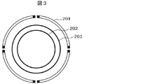
- FIG. 1 is a top view of main electron optical systems of a scanning electron microscope according to Example 1.
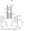
- FIG. 6 is a cross-sectional view of main electron optical systems of a scanning electron microscope according to Example 2.
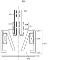
- FIG. 6 is a cross-sectional view of main electron optical systems of a scanning electron microscope according to Embodiment 3.
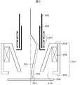
- FIG. 6 is a cross-sectional view of main electron optical systems of a scanning electron microscope according to Example 4.
- FIG. It is an electron orbit figure in the case of wide field deflection. It is an electron orbit figure in the case of an inclined beam.
- the main feature is that an electromagnetic deflector is provided above the electromagnetic lens directly above the sample, and an electrode for accelerating or decelerating electrons is provided so as to overlap with the electromagnetic deflector (for example, the height position overlaps with the vertical direction). . That is, the main feature is that an electrostatic lens is provided above the electromagnetic lens directly above the sample so as to overlap the electromagnetic deflector.
- the electrode By providing the electrode, it becomes possible to control the energy of electrons in the region where the electromagnetic deflector acts, and therefore it is possible to control the deflection chromatic aberration caused by the electromagnetic deflector. As a result, a tilt beam having a wide field deflection and a desired angle can be realized without interfering with the electromagnetic lens.
- FIG. 1 The first embodiment will be described with reference to FIGS. 1 to 3, 7 and 8.
- FIG. 1 The first embodiment will be described with reference to FIGS. 1 to 3, 7 and 8.
- FIG. 1 is an overall schematic diagram of a scanning electron microscope according to the first embodiment.
- the electron beam 102 emitted from the electron gun 101 is imaged on the sample by the condenser lens 103 and the electromagnetic lens 108.
- the objective lens is mainly composed of an electromagnetic lens 108 and an electrostatic lens generated by an electric field between the electromagnetic lens 108 and the sample 109.
- the secondary electrons and reflected electrons 104 emitted from the sample are detected by a detector 105 in the middle.
- the electron beam on the sample is scanned two-dimensionally by the electromagnetic deflector 106, and as a result, a two-dimensional image can be obtained.
- the two-dimensional image is displayed on the display device 119.
- Reference numeral 110 is a holder for placing a sample
- reference numeral 111 is an electron gun controller
- reference numeral 112 is a condenser lens controller
- reference numeral 114 is a scanning deflector controller
- reference numeral 115 is an electromagnetic lens controller
- reference numeral 116 is a sample voltage controller.
- Reference numeral 117 denotes a storage device
- reference numeral 118 denotes a control calculation unit of the entire apparatus.
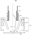
- FIG. 2 and 3 show a part of the electro-optical configuration in the apparatus.
- FIG. 2 is a schematic sectional view and FIG. 3 is a top view.
- the electromagnetic deflector 201 uses two stages in conjunction with each other, and a control electrode 202 capable of accelerating or decelerating electrons overlaps the electromagnetic deflector (with respect to the vertical direction). (Positions overlap).
- the inside of the control electrode has a cylindrical shape as shown in FIG. 3, and accelerates or decelerates electrons by applying a potential.
- the lower end of this electrode is above the opening 210 of the magnetic body of the electromagnetic lens 207 immediately above the sample, and avoids interference with the electromagnetic lens.
- the electromagnetic lens 207 is large and includes an upper magnetic path 204, a lower magnetic path 205, and an electromagnetic coil 206 made of a magnetic material.
- a positive potential is applied to a portion (upper magnetic path) 204 of the magnetic body of the electromagnetic lens, and axial aberrations are reduced by accelerating electrons.
- the additional electrode 203 exists above the upper end of the control electrode according to the present embodiment, and as a result, the electrostatic lens composed of three electrodes overlaps the electromagnetic deflector.
- the upper electrode is a ground electrode.
- Reference numeral 208 denotes a sample.
- the effect of the control electrode in this embodiment is first in controlling deflection chromatic aberration.
- deflection chromatic aberration is the most important aberration among deflection aberrations.
- the deflection chromatic aberration includes a deflection chromatic aberration caused by a deflector in which a difference in deflection sensitivity of the deflector is caused by a difference in electron velocity, and a deflection chromatic aberration caused by a lens in which a difference in focal length of the lens is caused by a difference in electron velocity. Since the final deflection chromatic aberration is the sum of the two, if the deflection chromatic aberration caused by the deflector changes, the final deflection chromatic aberration also changes.
- Fig. 7 shows a conceptual diagram of the electron orbit.
- Slow electrons having low energy with respect to the fast electron trajectory A701 both have a large deflection effect of the deflector and a lens effect of the lens.
- the low-speed electron trajectory A702 in FIG. 7 is a trajectory when only the deflection action works greatly, and the low-speed electron orbit B703 is a trajectory when only the lens action works greatly.
- the difference in position between the low-speed trajectory and the high-speed trajectory on the sample is the deflection chromatic aberration, which is the chromatic aberration caused by the deflector and the chromatic aberration caused by the lens, respectively.
- the chromatic aberration caused by the deflector acts in the direction in which the chromatic aberration caused by the lens is integrated.
- the deflection chromatic aberration caused by the deflector can be reduced, and the resolution can be prevented from deteriorating when deflecting a wide field of view.
- the electromagnetic deflector 201 and the control electrode 202 are installed apart from the electromagnetic lens, there are few physical restrictions, and compatibility with the electromagnetic lens 207 with a short focus and high resolution is possible.
- the deflection chromatic aberration caused by the lens mainly occurs in the vicinity of the sample, but a certain amount of the deflection chromatic aberration caused by the lens also occurs in this region.
- the control electrode 202 by applying a voltage to the control electrode 202, the potential difference from a portion (upper magnetic path) 204 of the magnetic material is reduced, and the lens effect is weakened, so that the deflection chromatic aberration due to the lens can be reduced. That is, the electromagnetic deflector 201 is disposed in the electrostatic lens above the electromagnetic lens 207, and an aberration reduction effect due to in-lens deflection is obtained.
- an additional electrode 203 exists between the electromagnetic deflector 201 and the control electrode 202. That is, there are double electrodes inside the position overlapping with the electromagnetic deflector 201. In this embodiment, electrons are accelerated or decelerated by the inner control electrode 202 of the two.
- the outer additional electrode 203 is grounded and serves as a vacuum partition for keeping the electron beam path in a vacuum. The effect of this structure is that the vacuum partition can be grounded by controlling the electron beam with a separate electrode from the vacuum partition, and the mechanical structure is simplified.
- the control electrode 202 has a structure spreading outward near the lower end, and shields the electron beam passage region from the external potential. This ensures the effect of the control electrode 202.
- Fig. 8 shows the electron trajectory when the tilted beam is formed.
- the slow electron trajectory C802 is obtained by increasing only the deflection action
- the slow electron trajectory D803 is obtained by increasing only the lens action.
- the deviation between the slow electron orbit D803 and the fast electron orbit B801 and the deviation between the slow electron orbit C and the fast electron orbit B are in the opposite directions.
- the resolution of the tilted beam can be improved by canceling the deflection chromatic aberration caused by the deflector that controls the deflection chromatic aberration caused by the lens, which is generated when the trajectory of the chromatic aberration tilted beam caused by the lens is made.
- the tilt angle there is a correlation between the tilt angle and the chromatic aberration caused by the lens, and the greater the canceling chromatic aberration, the larger the tilt angle can be obtained.
- the resolution of the electron beam tilted by 4 degrees could be 3 nm. This is a significant improvement in resolution compared to the conventional 7 nm. As a result, it is possible to observe the side wall of the reverse-tapered line pattern, and to manage the taper angle.
- this embodiment not only enables wide field of view deflection and tilted beam, but also allows switching only by changing the potential of the control electrode 202 according to each mode. Specifically, it accelerates in the wide field mode and decelerates in the tilt beam mode. In this case, since the control electrode is located above the electromagnetic lens, it is also a great feature that switching is possible without interference with the electromagnetic lens.
- a scanning electron microscope having a small aberration and a high resolution capable of realizing a wide field deflection and a tilted beam having a desired angle, and an inspection method using the same. I was able to.
- FIG. 4 shows a cross-sectional view of the main part of the electron optical configuration of the scanning electron microscope according to the present embodiment.
- the overall configuration of the apparatus is the same as that of the first embodiment.
- an electrostatic deflector 301 is provided on the control electrode 202.
- the electrostatic deflector 301 is for performing minute deflection.
- the electromagnetic deflector 201 largely deflects the electron beam on the sample surface, and then two-dimensional scanning is performed in conjunction with the two stages of the electrostatic deflector. I do. Since the electrostatic deflector 301 can increase the scanning speed (about 4 times that of the electromagnetic deflector), it is effective in suppressing charging of the insulator sample.
- the electrostatic deflector is installed above the control electrode in order to prevent interference between the electrostatic deflector and the control electrode.
- the electrostatic deflector used in this example is an octupole electrostatic deflector.
- a scanning electron microscope having a small aberration and a high resolution capable of realizing a wide field deflection and a tilted beam having a desired angle, and an inspection method using the same. I was able to. Further, by providing an electrostatic deflector, high resolution measurement could be realized even with an insulating film pattern.
- FIG. 5 shows a cross section of the main part of the electron optical configuration of the scanning electron microscope according to the present embodiment.
- the overall configuration of the apparatus is the same as that of the first embodiment.
- the control electrode 403 is short and the position of the electromagnetic deflector 201 overlaps, but does not necessarily cover the whole. The effect of this embodiment can be obtained even if the control electrode 403 partially overlaps the electromagnetic deflector 201.
- the effect of shortening the control electrode 403 is that the degree of freedom in the position of the electrostatic deflector 401 is increased.
- the deflection sensitivity can be increased by lowering the position of the electrostatic deflector 401.
- the resolution when the 50 ⁇ m square was deflected by the electromagnetic deflector was 3.3 nm. .
- higher resolution than the conventional 5 nm can be achieved.
- the uniformity in the visual field could be greatly improved to ⁇ 0.23 nm.
- a scanning electron microscope having a small aberration and a high resolution capable of realizing a wide field deflection and a tilted beam having a desired angle, and an inspection method using the same. I was able to. Moreover, by shortening the control electrode and bringing the electrostatic deflector and the electromagnetic deflector closer, the deflection sensitivity can be increased and higher resolution measurement can be performed.
- FIG. 6 shows a part of the electron optical configuration of the scanning electron microscope according to the present embodiment.
- the overall configuration of the apparatus is the same as that of the first embodiment.
- the control electrode is divided into an upper control electrode 502 and a lower control electrode 501. Different potentials can be applied to the respective electrodes, and more complicated electron velocity control is possible.
- the upper control electrode 502 and the lower control electrode 501 are arranged to overlap the upper deflector 504 and the lower deflector 503 of the electromagnetic deflector, respectively. As a result, the velocity of electrons in each deflector can be controlled.
- 2.8 kV is applied to the upper control electrode 502
- 3 kV is applied to the lower control electrode
- 6 kV is applied to a part of the magnetic material (upper magnetic path)
- ⁇ 2.7 kV is applied to the sample.
- the resolution when the angle is deflected is 2.8 nm, and high resolution scanning with a wide field of view can be realized.
- an 8-pole 2-stage electrostatic deflector is used as the offset superimposed electrostatic deflector 601. This applies the same offset voltage to the deflection voltage of each electrode of the electrostatic deflector. As a result, it is possible to reduce the chromatic aberration caused by the electrostatic deflector and the lens effect between the control electrode and the deflection chromatic aberration in the electrostatic deflection.
- an offset voltage of 2.8 kV the chromatic aberration of electrostatic deflection could be halved compared to the conventional case.
- a scanning electron microscope having a small aberration and a high resolution capable of realizing a wide field deflection and a tilted beam having a desired angle, and an inspection method using the same. I was able to.
- the use of an offset superimposed electrostatic deflector can reduce the aberration in electrostatic deflection.
- control electrodes of the previous examples have a continuous structure on the circuit, but it is clear that the same effect can be obtained even if the control electrodes are divided in the rotation direction.
- it can also be used as an electrostatic deflector.
- the electrostatic deflector also serves as a control electrode, thereby reducing the space occupied by the optical element and wiring. The number can be reduced.
- Electron gun 102 ... Electron beam, 103 ... Condenser lens, 104 ... Secondary electron and reflected electron, 105 ... Detector, 106 ... Electromagnetic deflector, 108 ... Electromagnetic lens, 109 ... Sample, 110 ... Holder, 111 ... Electron gun control unit 112... Condenser lens control unit 114. Scanning deflector control unit 115. Electromagnetic lens control unit 116. Sample voltage control unit 117 117 Storage device 118. Display device 201 ... Electromagnetic deflector 202 ... Control electrode 203 ... Additional electrode 204 ... Part of magnetic material (upper magnetic path) 205 ... Lower magnetic path 206 ...
- Electromagnetic coil 207 Electromagnetic lens 210 ... Magnetic body opening 301.
- Electrostatic deflector 401 Electrostatic deflector 403 Control electrode 501 Lower control electrode 502 Upper control electrode 503 Lower deflector 50 ... upper deflector, 601 ... offset superimposed electrostatic deflector, 701 ... fast electron orbit A, 702 ... slow electron orbit A, 703 ... slow electron orbit B, 801 ... fast electron orbit B, 802 ... slow electron orbit C, 803 ... Slow electron trajectory D.
Landscapes
- Chemical & Material Sciences (AREA)
- Analytical Chemistry (AREA)
- Testing Or Measuring Of Semiconductors Or The Like (AREA)
Abstract
Description
Claims (19)
- 電子源と、
前記電子源から放出された電子ビームを試料上に収束して照射する電磁レンズと、
前記試料から発生する2次電子信号や反射電子に基づいて試料像を得る手段と、
前記電磁レンズの上方に設けられた電磁偏向器と、
鉛直方向に対して高さ位置が前記電磁偏向器と重なる位置に、離間して設けられ、前記電子ビームを加速もしくは減速する制御電極とを有することを特徴とする走査電子顕微鏡。 - 請求項1記載の走査電子顕微鏡において、
前記電磁偏向器と制御電極の間に、更に付加電極を設けることを特徴とする走査電子顕微鏡。 - 請求項2記載の走査電子顕微鏡において、
前記付加電極が真空隔壁であることを特徴とする走査電子顕微鏡。 - 請求項1記載の走査電子顕微鏡において、
前記制御電極は下端近傍で外側に広がる構造になっていること特徴とする走査電子顕微鏡。 - 請求項1記載の走査電子顕微鏡において、
前記制御電極の下方に第2の制御電極を設けることを特徴とする走査電子顕微鏡。 - 請求項1記載の走査電子顕微鏡において、
前記電磁レンズの磁性体の1部に電位が印加されていることを特徴とする走査電子顕微鏡。 - 請求項5記載の走査電子顕微鏡において、
前記制御電極に、前記第2の制御電極や前記磁性体の1部に印加した正の電位より低い正の電位が印加されていることを特徴とする走査電子顕微鏡。 - 請求項1記載の走査電子顕微鏡において、
前記制御電極の上方に静電偏向器が配置されていることを特徴とする走査電子顕微鏡。 - 請求項8記載の走査電子顕微鏡において、
前記静電偏向器の各極にオフセット電位が印加されていることを特徴とする走査電子顕微鏡。 - 請求項1記載の走査電子顕微鏡において、
前記制御電極には正負の電位が印加出来ることを特徴とする走査電子顕微鏡。 - 請求項1記載の走査電子顕微鏡において、
前記制御電極は広視野モードでは加速し、傾斜ビームモードでは減速することを特徴とする走査電子顕微鏡。 - 電子源と、
前記電子源から放出された電子ビームを試料上に収束して照射する電磁レンズと、
前記試料から発生する2次電子信号や反射電子に基づいて試料像を得る手段と、
前記電磁レンズの上方に設けられた電磁偏向器と、
鉛直方向に対して高さ位置が前記電磁偏向器と重なる位置に、離間して設けられ、前記電子ビームを加速もしくは減速する2段の制御電極とを有することを特徴とする走査電子顕微鏡。 - 請求項12記載の走査電子顕微鏡において、
前記電磁偏向器が2段であり、上部の偏向器と上部の制御電極が、下部の偏向器と下部の制御電極がそれぞれ重なる位置に設けることを特徴とする走査電子顕微鏡。 - 請求項12記載の走査電子顕微鏡において、
前記制御電極が加速型であることを特徴とする走査電子顕微鏡。 - 請求項12記載の走査電子顕微鏡において、
前記制御電極が広視野モードでは加速型に、傾斜ビームモードでは減速型に、切り替え可能であることを特徴とする走査電子顕微鏡。 - 請求項1記載の走査電子顕微鏡を用いた検査方法であって、
前記電子ビームを前記制御電極により加速して前記試料に照射する工程と、
前記試料から発生する2次電子信号や反射電子に基づいて試料像を得る工程と、を有することを特徴とする検査方法。 - 請求項1記載の走査電子顕微鏡を用いた検査方法であって、
前記電子ビームを前記制御電極により減速し、斜め方向から前記試料に照射する工程と、
前記試料から発生する2次電子信号や反射電子に基づいて試料像を得る工程と、を有することを特徴とする検査方法。 - 請求項12記載の走査電子顕微鏡を用いた検査方法であって、
前記電子ビームを前記2段の制御電極により加速して前記試料に照射する工程と、
前記試料から発生する2次電子信号や反射電子に基づいて試料像を得る工程と、を有することを特徴とする検査方法。 - 請求項12記載の走査電子顕微鏡を用いた検査方法であって、
前記電子ビームを前記2段の制御電極により減速し、斜め方向から前記試料に照射する工程と、
前記試料から発生する2次電子信号や反射電子に基づいて試料像を得る工程と、を有することを特徴とする検査方法。
Priority Applications (2)
| Application Number | Priority Date | Filing Date | Title |
|---|---|---|---|
| JP2012503059A JP5308572B2 (ja) | 2010-03-02 | 2011-02-18 | 走査電子顕微鏡及びそれを用いた検査方法 |
| US13/521,254 US8637820B2 (en) | 2010-03-02 | 2011-02-18 | Scanning electron microscope and inspection method using same |
Applications Claiming Priority (2)
| Application Number | Priority Date | Filing Date | Title |
|---|---|---|---|
| JP2010-045509 | 2010-03-02 | ||
| JP2010045509 | 2010-03-02 |
Publications (1)
| Publication Number | Publication Date |
|---|---|
| WO2011108368A1 true WO2011108368A1 (ja) | 2011-09-09 |
Family
ID=44542029
Family Applications (1)
| Application Number | Title | Priority Date | Filing Date |
|---|---|---|---|
| PCT/JP2011/053440 Ceased WO2011108368A1 (ja) | 2010-03-02 | 2011-02-18 | 走査電子顕微鏡及びそれを用いた検査方法 |
Country Status (3)
| Country | Link |
|---|---|
| US (1) | US8637820B2 (ja) |
| JP (1) | JP5308572B2 (ja) |
| WO (1) | WO2011108368A1 (ja) |
Cited By (3)
| Publication number | Priority date | Publication date | Assignee | Title |
|---|---|---|---|---|
| WO2013161684A1 (ja) * | 2012-04-24 | 2013-10-31 | 株式会社日立ハイテクノロジーズ | 荷電粒子線装置 |
| JP2015162265A (ja) * | 2014-02-25 | 2015-09-07 | 株式会社ホロン | 静電型回転場偏向器を用いた荷電粒子線装置 |
| WO2015166849A1 (ja) * | 2014-04-28 | 2015-11-05 | 株式会社日立ハイテクノロジーズ | 電子線装置 |
Families Citing this family (4)
| Publication number | Priority date | Publication date | Assignee | Title |
|---|---|---|---|---|
| US8921782B2 (en) * | 2012-11-30 | 2014-12-30 | Kla-Tencor Corporation | Tilt-imaging scanning electron microscope |
| CN108807118B (zh) * | 2018-06-08 | 2024-05-07 | 聚束科技(北京)有限公司 | 一种扫描电子显微镜系统及样品探测方法 |
| TWI854246B (zh) | 2021-08-23 | 2024-09-01 | 日商紐富來科技股份有限公司 | 多帶電粒子束描繪方法及多帶電粒子束描繪裝置 |
| CN120432373A (zh) * | 2025-04-29 | 2025-08-05 | 东方晶源微电子科技(北京)股份有限公司 | 电子束装置 |
Citations (5)
| Publication number | Priority date | Publication date | Assignee | Title |
|---|---|---|---|---|
| JPS62219445A (ja) * | 1986-03-20 | 1987-09-26 | Jeol Ltd | 電子線装置 |
| JPH08195345A (ja) * | 1994-11-18 | 1996-07-30 | Hitachi Ltd | 電子ビーム描画装置 |
| JPH11162384A (ja) * | 1997-11-27 | 1999-06-18 | Hitachi Ltd | 走査電子顕微鏡 |
| JP2001015055A (ja) * | 1999-04-15 | 2001-01-19 | Applied Materials Inc | 荷電粒子ビームカラム |
| JP2006294962A (ja) * | 2005-04-13 | 2006-10-26 | Hitachi High-Technologies Corp | 電子ビーム描画装置および描画方法 |
Family Cites Families (13)
| Publication number | Priority date | Publication date | Assignee | Title |
|---|---|---|---|---|
| US4340481A (en) * | 1975-02-15 | 1982-07-20 | Asahi Kasei Kogyo Kabushiki | Membrane filtration type hollow fibers |
| JPH08138611A (ja) | 1994-11-04 | 1996-05-31 | Nikon Corp | 荷電粒子線装置 |
| US6452175B1 (en) | 1999-04-15 | 2002-09-17 | Applied Materials, Inc. | Column for charged particle beam device |
| US7223974B2 (en) * | 2002-05-22 | 2007-05-29 | Applied Materials, Israel, Ltd. | Charged particle beam column and method for directing a charged particle beam |
| US7800062B2 (en) * | 2002-06-11 | 2010-09-21 | Applied Materials, Inc. | Method and system for the examination of specimen |
| US6825475B2 (en) * | 2002-09-19 | 2004-11-30 | Applied Materials Israel, Ltd. | Deflection method and system for use in a charged particle beam column |
| US7034297B2 (en) * | 2003-03-05 | 2006-04-25 | Applied Materials, Israel, Ltd. | Method and system for use in the monitoring of samples with a charged particle beam |
| US7170068B2 (en) * | 2005-05-12 | 2007-01-30 | Applied Materials, Israel, Ltd. | Method and system for discharging a sample |
| JP5185506B2 (ja) * | 2006-03-23 | 2013-04-17 | 株式会社日立ハイテクノロジーズ | 荷電粒子線パターン測定装置 |
| US7525091B2 (en) * | 2006-08-23 | 2009-04-28 | Applied Materials, Israel, Ltd. | Charged particle beam system and a method for inspecting a sample |
| JP5237728B2 (ja) * | 2008-08-29 | 2013-07-17 | 日本電子株式会社 | 粒子線装置 |
| EP2518755B1 (en) * | 2011-04-26 | 2014-10-15 | FEI Company | In-column detector for particle-optical column |
| EP2573796B1 (en) * | 2011-09-22 | 2014-05-07 | Carl Zeiss Microscopy Limited | Particle beam system having a hollow light guide |
-
2011
- 2011-02-18 US US13/521,254 patent/US8637820B2/en not_active Expired - Fee Related
- 2011-02-18 JP JP2012503059A patent/JP5308572B2/ja not_active Expired - Fee Related
- 2011-02-18 WO PCT/JP2011/053440 patent/WO2011108368A1/ja not_active Ceased
Patent Citations (5)
| Publication number | Priority date | Publication date | Assignee | Title |
|---|---|---|---|---|
| JPS62219445A (ja) * | 1986-03-20 | 1987-09-26 | Jeol Ltd | 電子線装置 |
| JPH08195345A (ja) * | 1994-11-18 | 1996-07-30 | Hitachi Ltd | 電子ビーム描画装置 |
| JPH11162384A (ja) * | 1997-11-27 | 1999-06-18 | Hitachi Ltd | 走査電子顕微鏡 |
| JP2001015055A (ja) * | 1999-04-15 | 2001-01-19 | Applied Materials Inc | 荷電粒子ビームカラム |
| JP2006294962A (ja) * | 2005-04-13 | 2006-10-26 | Hitachi High-Technologies Corp | 電子ビーム描画装置および描画方法 |
Cited By (8)
| Publication number | Priority date | Publication date | Assignee | Title |
|---|---|---|---|---|
| WO2013161684A1 (ja) * | 2012-04-24 | 2013-10-31 | 株式会社日立ハイテクノロジーズ | 荷電粒子線装置 |
| JP2013229104A (ja) * | 2012-04-24 | 2013-11-07 | Hitachi High-Technologies Corp | 荷電粒子線装置 |
| US9312091B2 (en) | 2012-04-24 | 2016-04-12 | Hitachi High-Technologies Corporation | Charged particle beam apparatus |
| JP2015162265A (ja) * | 2014-02-25 | 2015-09-07 | 株式会社ホロン | 静電型回転場偏向器を用いた荷電粒子線装置 |
| WO2015166849A1 (ja) * | 2014-04-28 | 2015-11-05 | 株式会社日立ハイテクノロジーズ | 電子線装置 |
| CN106165054A (zh) * | 2014-04-28 | 2016-11-23 | 株式会社日立高新技术 | 电子线装置 |
| US9966218B2 (en) | 2014-04-28 | 2018-05-08 | Hitachi High-Technologies Corporation | Electron beam device |
| CN106165054B (zh) * | 2014-04-28 | 2018-08-28 | 株式会社日立高新技术 | 电子线装置 |
Also Published As
| Publication number | Publication date |
|---|---|
| JPWO2011108368A1 (ja) | 2013-06-24 |
| JP5308572B2 (ja) | 2013-10-09 |
| US20120286158A1 (en) | 2012-11-15 |
| US8637820B2 (en) | 2014-01-28 |
Similar Documents
| Publication | Publication Date | Title |
|---|---|---|
| US20220392734A1 (en) | Certain improvements of multi-beam generating and multi-beam deflecting units | |
| JP5308572B2 (ja) | 走査電子顕微鏡及びそれを用いた検査方法 | |
| JP4215282B2 (ja) | 静電対物レンズ及び電気走査装置を装備したsem | |
| EP1703538B1 (en) | Charged particle beam device for high spatial resolution and multiple perspective imaging | |
| US8921782B2 (en) | Tilt-imaging scanning electron microscope | |
| JP5791060B2 (ja) | 電子ビームウェーハ検査システム及びその作動方法 | |
| CN1666101B (zh) | 带电粒子束装置和侦测样本的方法 | |
| WO2016121225A1 (ja) | 荷電粒子線装置及び走査電子顕微鏡 | |
| US6897442B2 (en) | Objective lens arrangement for use in a charged particle beam column | |
| US9543053B2 (en) | Electron beam equipment | |
| JP2014220241A5 (ja) | ||
| JP4141211B2 (ja) | 粒子ビーム装置 | |
| JP5492306B2 (ja) | 電子ビーム装置 | |
| US20040173746A1 (en) | Method and system for use in the monitoring of samples with a charged particles beam | |
| JP4006946B2 (ja) | 走査電子顕微鏡 | |
| KR100518812B1 (ko) | 주사 전자 현미경과 그 유사 장치에서 빈 필터에 의해발생되는 광행차의 감소 | |
| JP5478683B2 (ja) | 荷電粒子線の照射方法及び荷電粒子線装置 | |
| JP6462729B2 (ja) | 荷電粒子線装置及び走査電子顕微鏡 | |
| WO2019049261A1 (ja) | 電子銃および電子ビーム応用装置 | |
| WO2016121226A1 (ja) | 荷電粒子線装置及び走査電子顕微鏡 | |
| JP4128487B2 (ja) | 荷電粒子線装置 | |
| JPH0864163A (ja) | 荷電粒子ビーム装置 | |
| JP2005063983A (ja) | 走査電子顕微鏡 | |
| JP4792074B2 (ja) | 基板検査方法および基板検査装置 | |
| JP2012173008A (ja) | 光電子顕微鏡 |
Legal Events
| Date | Code | Title | Description |
|---|---|---|---|
| 121 | Ep: the epo has been informed by wipo that ep was designated in this application |
Ref document number: 11750480 Country of ref document: EP Kind code of ref document: A1 |
|
| WWE | Wipo information: entry into national phase |
Ref document number: 13521254 Country of ref document: US |
|
| WWE | Wipo information: entry into national phase |
Ref document number: 2012503059 Country of ref document: JP |
|
| NENP | Non-entry into the national phase |
Ref country code: DE |
|
| 122 | Ep: pct application non-entry in european phase |
Ref document number: 11750480 Country of ref document: EP Kind code of ref document: A1 |