WO2011105272A1 - 有機光電変換デバイスの製造方法 - Google Patents
有機光電変換デバイスの製造方法 Download PDFInfo
- Publication number
- WO2011105272A1 WO2011105272A1 PCT/JP2011/053335 JP2011053335W WO2011105272A1 WO 2011105272 A1 WO2011105272 A1 WO 2011105272A1 JP 2011053335 W JP2011053335 W JP 2011053335W WO 2011105272 A1 WO2011105272 A1 WO 2011105272A1
- Authority
- WO
- WIPO (PCT)
- Prior art keywords
- film
- layer
- photoelectric conversion
- organic
- rolling
- Prior art date
- Legal status (The legal status is an assumption and is not a legal conclusion. Google has not performed a legal analysis and makes no representation as to the accuracy of the status listed.)
- Ceased
Links
Images



Classifications
-
- H—ELECTRICITY
- H10—SEMICONDUCTOR DEVICES; ELECTRIC SOLID-STATE DEVICES NOT OTHERWISE PROVIDED FOR
- H10K—ORGANIC ELECTRIC SOLID-STATE DEVICES
- H10K71/00—Manufacture or treatment specially adapted for the organic devices covered by this subclass
- H10K71/50—Forming devices by joining two substrates together, e.g. lamination techniques
-
- H—ELECTRICITY
- H10—SEMICONDUCTOR DEVICES; ELECTRIC SOLID-STATE DEVICES NOT OTHERWISE PROVIDED FOR
- H10K—ORGANIC ELECTRIC SOLID-STATE DEVICES
- H10K77/00—Constructional details of devices covered by this subclass and not covered by groups H10K10/80, H10K30/80, H10K50/80 or H10K59/80
- H10K77/10—Substrates, e.g. flexible substrates
- H10K77/111—Flexible substrates
-
- Y—GENERAL TAGGING OF NEW TECHNOLOGICAL DEVELOPMENTS; GENERAL TAGGING OF CROSS-SECTIONAL TECHNOLOGIES SPANNING OVER SEVERAL SECTIONS OF THE IPC; TECHNICAL SUBJECTS COVERED BY FORMER USPC CROSS-REFERENCE ART COLLECTIONS [XRACs] AND DIGESTS
- Y02—TECHNOLOGIES OR APPLICATIONS FOR MITIGATION OR ADAPTATION AGAINST CLIMATE CHANGE
- Y02E—REDUCTION OF GREENHOUSE GAS [GHG] EMISSIONS, RELATED TO ENERGY GENERATION, TRANSMISSION OR DISTRIBUTION
- Y02E10/00—Energy generation through renewable energy sources
- Y02E10/50—Photovoltaic [PV] energy
- Y02E10/549—Organic PV cells
-
- Y—GENERAL TAGGING OF NEW TECHNOLOGICAL DEVELOPMENTS; GENERAL TAGGING OF CROSS-SECTIONAL TECHNOLOGIES SPANNING OVER SEVERAL SECTIONS OF THE IPC; TECHNICAL SUBJECTS COVERED BY FORMER USPC CROSS-REFERENCE ART COLLECTIONS [XRACs] AND DIGESTS
- Y02—TECHNOLOGIES OR APPLICATIONS FOR MITIGATION OR ADAPTATION AGAINST CLIMATE CHANGE
- Y02P—CLIMATE CHANGE MITIGATION TECHNOLOGIES IN THE PRODUCTION OR PROCESSING OF GOODS
- Y02P70/00—Climate change mitigation technologies in the production process for final industrial or consumer products
- Y02P70/50—Manufacturing or production processes characterised by the final manufactured product
Definitions
- the present invention relates to a method for producing an organic photoelectric conversion device, in particular, a method for producing a polymer organic photoelectric conversion device.
- Organic photoelectric conversion devices such as organic EL light-emitting elements
- organic EL light-emitting elements are being researched and developed in low molecular weight materials and high molecular weight materials for the purpose of application to lighting, displays, etc., and commercialization is also progressing gradually.
- the emission characteristics of recent organic EL light emitting devices of low molecular weight materials are based on the multilayer structure in which films with functions such as carrier injection, transport, blocking, and light emission are stacked, and the use of triplet excitons by phosphorescent materials. Luminous efficiency has been greatly improved.
- the peak value of white power efficiency is 64 lm / W, 34 lm / W at 1,000 cd / m 2 , and the energy utilization of a conventional incandescent lamp The efficiency (12 to 17 lm / W) has been exceeded (see Non-Patent Document 1).
- a general manufacturing method of a low molecular weight organic EL light emitting element is to form each layer of organic EL and a cathode in a vacuum system on a glass substrate on which a transparent electrode such as ITO is formed.
- mass production technology is progressing, such as increasing the deposition rate by using a linear deposition source to deal with a large area and bringing the evaporation source closer to the substrate.
- it has not yet reached the cost, performance, and reliability of existing LCDs and fluorescent lamps.
- the basic idea is that, unlike a low-molecular layer structure of single-functional films, the functions are concentrated in one molecule and in principle a single-layer device structure. Film formation is coating, and there is a great merit in principle in terms of productivity, such as the possibility of applying a roll-to-roll method using a plastic substrate.
- a conjugated polymer which is a typical material has a charge transport function and a light emission function due to delocalization of ⁇ electrons on a chain skeleton. Therefore, one-dimensional LED can be formed with one molecule in principle by copolymerization of monomers having respective functions.
- the low molecular weight system is the closest to the practical stage at present, but the productivity is essentially the deposition rate, and the reliability is essentially the result of the deposition film formation principle and characteristics of crystallization from amorphous. I have a problem.
- polymer systems currently do not have low performance and reliability, but there is no substantial difference between low molecules and polymers in terms of light emission and charge transport functions.
- a polymer system it is structurally stable due to molecular bonds such as a chain, and the degree of crystallization is less than that of a low molecular system. Therefore, it is reasonable to consider that this difference is caused by the polymer film quality and device structure actually formed.
- the polymer film is formed by coating, so the solvent always remains.
- High polymer systems have been said to be superior to low molecular weight systems in terms of productivity, but the reason for this is that the EL function is one molecule as in the case of conjugated polymers. Therefore, a single-layer device structure can be formed by coating. However, in reality, a multilayer structure is required as described above. Therefore, it is essentially difficult to draw out ideal performance as long as coating film formation is performed.
- the present invention has been proposed in view of the above, and an object of the present invention is to realize a high-molecular organic photoelectric conversion device with a multilayer structure similar to a low-molecular organic photoelectric conversion device.
- Means for solving the above problems are as follows.
- Manufacturing method of organic photoelectric conversion device is described.
- a multilayer structure similar to that of a low-molecular organic photoelectric conversion device can be realized by forming the polymer organic photoelectric conversion device by the same technique as that of a plastic film manufacturing method currently industrialized.
- Polymer materials are more diverse than low-molecular materials, and can control the spatial arrangement of functional units against the backdrop of plastic molding as well as individual molecular designs.
- impurities are greatly reduced, resulting in a high-quality film.
- the structure is more stable than that of low molecular weight systems and the resistance to water and oxygen is high.
- the film production speed in extrusion molding, rolling, stretching, etc. is as high as several hundreds m / min and the apparatus cost is low, so that the mass production is high and the low cost required for lighting applications can be realized.
- FIG. 1 which shows typically composition (a) of a polymer organic electroluminescent light emitting element, and an illuminating device (b) using the same Schematic diagram showing a manufacturing method in which an organic EL film formed by extrusion is laminated to an anode substrate to form a cathode electrode
- Diagram showing the principle configuration of multilayer extruder (a) and the principle of multilayer thin film formation
- Schematic diagram showing a manufacturing method for forming a cathode electrode by thinning an extruded organic EL film by rolling and stretching, laminating it on an anode substrate
- Schematic diagram showing a manufacturing method using an auxiliary substrate for rolling and stretching Diagram showing the structure of the anode substrate Schematic diagram of cathode and passivation film forming apparatus
- FIG. 1 (a) shows an organic EL device structure obtained by the present invention.
- a polymer organic EL film 2 is bonded to an anode substrate 1 serving as an electrode substrate, and a cathode electrode 3 is added thereon.
- the surface of the anode substrate is made of an ITO electrode and an insulating film partially covering the ITO electrode, and the anode terminal 4 is formed on the back surface of the substrate. It is manufactured in the form of a continuous tape in which a polymer organic EL film and a cathode electrode are continuously laminated, and the entire surface is covered with a passivation film 6 (a part of which is shown in the figure).
- the cathode electrode is formed by vapor deposition as will be described later.
- the cathode terminal 5 is placed on the cathode electrode surface.
- the tape is cut so that both terminals come to the ends, and this becomes the unit linear light emitter 7.
- the linear light emitters are arranged in a plane and a portion of the passivation film is removed to expose the anode and cathode terminals, which are connected by common terminal lead lines 8 and 9, respectively. Configure flat illumination.
- FIG. 2 schematically shows adhesion of the polymer organic EL film 2 in FIG. 1 to the anode substrate.
- the film-like anode substrate 11 is wound around a reel 10 and travels by a reel-to-reel (RtR) mechanism (one winding reel is not shown in the figure).
- the polymer organic EL film 12 formed by extrusion from the multilayer extruder 14 is made into a thin film by a rolling or stretching roller 16 and pressed onto the anode substrate 11 by a laminating roller 15.
- the cathode electrode and the passivation film are continuously added in the vapor deposition machine 13.
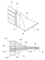
- only one stage of rolling or stretching rollers is shown, but it goes without saying that multiple stages are used depending on the film thickness. This also applies to the following drawings.
- FIG. 3A is a principle configuration diagram of a multilayer extrusion molding machine.
- the organic EL material melted by the extruder 20 is introduced into the feed block 21.
- a multi-layer prototype having a space and a layer order proportional to the film thickness of each layer is formed in the multi-layer manifold 22, formed to a final film thickness by the T-die mold 23, and injected from the exit slit 24.
- FIG. 3 (b) schematically shows a state in which a four-layer film is formed in the longitudinal section of the central portion of this configuration.
- parallel flows of laminar flows 32-1 to 32-4 having different thicknesses are formed, and then flow into the T-die mold 23 to gradually reduce the film thickness in proportion.
- a multilayer film 35 having a film thickness and width determined by the die exit slit 34 is formed.
- FIG. 4 shows a method of dividing the organic EL layer into several, and installing a plurality of extruders corresponding to each of the organic EL layers as shown in FIG. Indicates.
- the film-like anode substrate 41 is wound around a reel 40 and travels by an RtR mechanism (one winding reel is not shown in the figure).
- the polymer organic EL film formed by extrusion from the single-layer or multilayer extruder 42-1 is thinned by a rolling or stretching machine 43-1 and pressed onto the anode substrate 41 by a laminating roller 44-1. Thereafter, the single layer or multilayer extruders 42-2 and 42-3 are similarly laminated on the previous polymer organic EL film.
- a cathode electrode and a passivation film are continuously added in the vapor deposition machine 45.
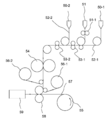
- FIG. 5 shows a method of thinning a polymer organic EL multilayer film extruded using a base film.
- the film On the base film 52-1 having a thickness of the order of mm formed by the extrusion molding machine 50-1, the film is formed by the multilayer extrusion molding machine 51 for polymer organic EL and further thinned by the rolling or stretching roller 51-1.
- the molecular organic EL multilayer film is laminated by a laminating roller 53-1.
- a base film 52-2 having a thickness of the order of mm is formed by an extruder 50-2, and is laminated on the polymer organic EL multilayer film by a laminating roller 53-2.
- the laminated film is thinned by a rolling or stretching machine 54, and the base film is taken up by base film take-up rollers 56-1 and 56-2.
- the polymer organic EL film is wound around a laminating roller 58 and then laminated on an anode substrate 57 that is wound around a reel 55 and travels by an RtR mechanism, and a cathode electrode is formed by a vapor deposition device 59. 4 and 5, the film is thinned by rolling and stretching following extrusion molding. However, when the film is sufficiently thinned by extrusion molding, the rolling and stretching processes can be omitted.
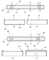
- FIG. 6 shows the structure of the film-like anode substrate.
- the substrate material is mainly transparent plastic, and the ITO electrode 61 is formed on a wide roll, and the continuous tape 60 slit to the width to be used is used as the base tape of the anode substrate.
- Reference numeral 68 denotes a through hole of the substrate, which is used for monitoring the tape running and positioning the cathode portion.
- Cu is formed on the entire surface of the base tape by sputtering or the like, and the Cu on the ITO is removed by etching leaving the peripheral portion of the base tape by a photolithography process as shown in FIG. 62 is formed.
- FIG. 6B corresponding to the A-A ′ cross section of FIG. 6, a part of Cu on the back surface of the base tape is left to be an anode terminal 63.
- FIG. 6 (c) corresponding to the cross-section B-B 'in FIG. 6 (a)
- Cu on the back surface other than the terminal portion is removed to become an EL light emission surface.
- F and G in FIGS. 6 (a) and 6 (d) are cutting parts.
- Reference numeral 64 in FIG. 6 (c) is a side cross section of the ITO reinforcing electrode, and shows contact with ITO. Further, Ni, Au or the like is plated on this surface to greatly reduce the voltage drop due to ITO resistance.
- the side surface and the peripheral portion of the base tape are covered with the SiOx insulating layer 65, and in particular, the SiOx layer 66 corresponding to the cathode terminal portion is provided on a part of the ITO surface.
- This film provides insulation between the anode and the cathode.
- 6E shows a C-C ′ cross section of FIG. 6D
- FIG. 6F shows an E-E ′ cross section.
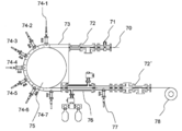
- FIG. 7 shows a method of continuously forming a cathode electrode on an anode substrate base tape laminated with a polymer organic EL film by running RtR as shown in FIG. 2, FIG. 4, and FIG.
- the anode substrate 70 laminated with the polymer organic EL film is introduced into the cathode deposition chamber 73 through the atmospheric pressure plasma surface treatment 71 and the differential exhaust system 72.
- the base tape is in close contact with the rotating drum 75, and a cathode electrode is formed by a plurality of LiF or MoOx and Al vapor deposition sources 74.
- a multi-layered organic passivation deposition system 76 and an oxide deposition system 77 are used to form a passivation layer of an alternating oxide film-organic film (only one stage is shown in the figure), and then through a differential exhaust system 72 '. And is wound on a reel 78.
- Example 1 As a starting material for the anode substrate, a 0.1 mm thick wide PEN roll film sputtered with ITO was cut into a 20 mm wide reel by a slitter. This reel was sputtered with a mask having a width of 18 mm on the ITO surface with a magnetron sputtering device incorporating an RtR mechanism, the remaining portion was sputtered with 100 nm of Cu, and Cu removal on the back surface and electrode formation were performed using an RtR photolithographic device.
- the polymer organic EL material As the polymer organic EL material, a dispersion system in which the base material is PVK (poly (N-vinylcarbazole)) was used.
- the hole transport layer was doped with PVK-PEDOT, the electron transport layer was PVK-PBD, and the light-emitting layer was doped with a low-molecular light emitter in PVK.
- Coumarin 6 was used for green, DCM for red, and TPB for blue.
- the final film thickness was 75 to 80 nm for each charge transport layer, 15 nm for each light emitting layer, and the total film thickness of 5 layers was 200 nm.
- the manifold of the multi-layer extrusion molding machine for 5 layers was made into the space
- die was 5 micrometers, and the width
- the inner surface of the T-die mold was subjected to CMP polishing, and DLC (DiamondiaLike Carbon) was coated by CVD.
- the organic EL film coming out from the outlet of the T-die mold is thinned by a five-stage hot rolling roller and pressed onto the anode substrate tape by the mechanism shown in FIG. 2, and this is applied to the RtR cathode and the passivation composition shown in FIG.
- the cathode was deposited with 0.5 nm LiF and 300 nm Al.
- the passivation film was formed by stacking 5 pairs with a multilayer structure in which SiOx film 30 nm and polyurea-based compound vapor-deposited polymer film 2 ⁇ m were alternately stacked.
- Example 2 As a starting material for the anode substrate, a 0.1 mm thick wide PEN roll film sputtered with ITO was cut into a 20 mm wide reel by a slitter. This reel was sputtered with a mask having a width of 18 mm on the ITO surface with a magnetron sputtering device incorporating an RtR mechanism, the remaining portion was sputtered with 100 nm of Cu, and Cu removal on the back surface and electrode formation were performed using an RtR photolithographic device.
- the hole transport layer is a polymer having TPD in the side chain
- the electron transport layer is a polymer having PBD in the side chain
- the light emitting layer is phosphorescence corresponding to iridium complex RGB in the side chain.
- Polymers having respective materials were used.
- the final film thickness was 75 to 80 nm for each charge transport layer, 15 nm for each light emitting layer, and the total film thickness of 5 layers was 200 nm.
- a multilayer extruder for RGB light emitting layer 3 layers, an extruder for each of hole and electron transport layers and an individual extruder were used.
- the exit slit gap of the T-die mold for the light emitting layer, hole, and electron transport layer was 5 ⁇ m, and the width was all 18 mm.
- the inner surface of each T-die mold was subjected to CMP polishing, and DLC was coated by CVD.
- the extruded film was immediately uniaxially stretched to a given thickness by a 5-stage hot roller without cooling.
- the surface of the hot roller was finished to a surface roughness of about 1 nm using EEM (Elast Emission Machining) for surface processing and final finishing by plasma CVM (Chemical Vaporization Machining).
- the organic EL film having reached the final film thickness is pressure-bonded to the anode substrate tape by the mechanism shown in FIG. 4, and this is the RtR cathode and passivation film forming machine shown in FIG. Was evaporated at 300 nm.
- the passivation film 5 pairs were laminated in a multilayer structure in which SiOx films 30 nm and polyurea-based compound vapor-deposited polymer films 2 ⁇ m were alternately stacked.
- the present invention has been described above by exemplifying the polymer organic EL elements as Examples 1 and 2.
- the present invention is not limited to this, and the polymer organic photoelectric conversion device in general includes a solar cell using a polymer organic material. Applicable to the manufacture of
Landscapes
- Engineering & Computer Science (AREA)
- Manufacturing & Machinery (AREA)
- Electroluminescent Light Sources (AREA)
- Photovoltaic Devices (AREA)
Abstract
本発明の課題は、高分子有機光電変換デバイスを低分子有機光電変換デバイスと同様な多層構造を実現することである。 フィルム状の電極基板を用意する工程と、高分子有機材料を光電変換機能が生ずる順に重ねた層を多層押出成形する工程と、該層を圧延ないし延伸によって成形する工程と、該フィルム状の電極基板上に圧延ないし延伸によって成形された該層をラミネートする工程とを含む有機光電変換デバイスの製造方法である。
Description
本発明は、有機光電変換デバイスの製造方法、特に高分子有機光電変換デバイスの製造方法に関するものである。
有機光電変換デバイス、例えば有機EL発光素子は、照明、ディスプレイ等への適用を目標に低分子系材料、高分子系材料において研究開発が進められ、製品化も徐々に進んでいる。最近の低分子系材料の有機EL発光素子の発光特性は、キャリアの注入、輸送、ブロック、発光等それぞれの機能を持つ膜を積層した多層構造と燐光材料による三重項励起子の利用によって全体の発光効率が大きく向上してきた。特に、発光層をRGBに対応した3層のドーピング層にした例では、白色のパワー効率のピーク値として64lm/W、1、000cd/m2で34lm/Wと、従来の白熱灯のエネルギー利用効率(12~17lm/W)を超えるようになってきた(非特許文献1参照)。
低分子系有機EL発光素子の一般的な製造方法は、ITO等の透明電極を成膜したガラス基板上に真空系で有機EL各層、陰極を形成する。生産技術の面では、線状蒸着源により大面積に対応し、蒸発源を基板に近接させ蒸着レートを上げる等の量産技術が進展しつつある。しかしながら既存のLCD、蛍光灯等に対してコスト、性能、信頼性の面でまだ及ばない。
次に高分子材料の場合、低分子系における単機能膜の積層構造と違い、一つの分子に機能を集約し原理的には単層のデバイス構造というのが基本的な考え方である。成膜は塗布であり、プラスチック基板を用いたロール・ツウ・ロール方式の適用の可能性等生産性の面で原理的に大きなメリットがある。典型的な材料である共役系高分子は、鎖状の骨格上のπ電子の非局在性により電荷輸送機能と発光機能を有する。従ってそれぞれの機能を持つモノマーの共重合により原理的に一分子で一次元のLEDを形成することができる。
しかしながら現実には正孔輸送層と発光・電子輸送層の2層積層構造、またチャージバランス、信頼性等の面から正孔注入層上にインターレイヤーを必要とする。このように実際には単層で輸送、発光の機能を両立させることは中々難しい上、このような層構造に於いてもパワー効率は10lm/Wの程度と低分子系と比較すると非常に低い(例えば、非特許文献2参照)。
高分子系の多層化は塗布のため下地膜の溶解、加熱の影響等を考慮すると組み合わされる材料と層数が限定され、実際上は2~3層が限度である。塗布された膜を架橋構造にして、上層を塗布する際の溶解を防ごうという提案はあるが(特許文献1、2等)、未だデバイス化されたという報告はない。
このように低分子系が目下製品化に最も近いレベルにあり、実際にディスプレイへの実用化が進んでいるが、照明デバイスへの適用を考えた場合、上記性能では現行の標準的な照明体である蛍光灯に未だ及ばない。即ち、蛍光灯の場合輝度レベルは10,000cd/ m2以上、そのレベルでの効率100lm/W以上、寿命40型で12,000時間以上である。特に低分子系では高効率が実現されていると言われているが、性能の発表データの殆どが2mm平方程度の小面積での値であり、この面積を僅か数cm2程度に拡大しただけで途端に効率、信頼性が低下する。これは大面積基板を扱う真空蒸着量産装置での不純物、パーティクル、膜厚の不均一性等の制御の難しさを示唆している。
照明装置への適用を考える場合の更に重要な因子は、コストである。照明製品の市場価格はディスプレイの1/10以下である。この観点から見ると低分子系の生産性に本質的な問題がある。即ち、低分子系の蒸着レートは高々0.2~0.3nm/s程度で現行TFTの成膜レートよりも1桁以上低い。従って、蛍光灯と同一効率でも100倍の生産性向上が必要となる。
しかしながら一般に成膜レートを上げると膜質が低下すること、通電、経時による分子結合形態(morphology)の変化等蒸着膜には原理的に検討すべき点が多い。また、発光層等はゲスト分子を少量ドープするが、量産レベルでの多元蒸着の空間的、時間的安定化も大きな問題である。更に低分子系の膜は本質的にはフレキシブルではないので、高信頼化のためにはガラス基板が必須で、従ってこれに対する生産装置は枚葉式装置となり、装置の機構面からも生産性に制限が出てくる。このように、低分子系は目下実用の段階に最も近いと言われているが、その生産性は蒸着レート、信頼性はアモルファスからの結晶化という蒸着成膜の原理、特性に帰着する本質的問題を抱えている。
一方、高分子系は目下性能、信頼性共に低分子に及ばないが、発光、電荷輸送機能に関して低分子と高分子で本質的な差がある訳でない。また高分子系の場合は鎖状等の分子結合により構造的に安定であり、結晶化の程度は低分子系よりも少ない。従ってこの差は実際に形成されている高分子の膜質とデバイス構造に原因があると考えるのが妥当であろう。膜質について言えば高分子膜は塗布で形成されるため溶媒は必ず残留する。
実際、塗布膜から溶媒を完全に除去しようとすると高真空中で1時間以上の加熱が必要であり、高分子膜の性能データはこのような処理を行ったものが多い。この他高分子材料の精製、分子量分布等の問題、特に溶媒に溶ける分子構造とするため使える有機EL材料の制限及び可溶化構造とすることによる性能の変化等の影響が考えられる。デバイス構造の面からは、単層ないし2層構造ではチャージバランスをとるのが困難であることが推測される。
高分子系は、生産性に優れていることが、低分子系に較べて優位であると言われて来たが、その根拠は、共役系高分子の場合のようにEL機能を一個の分子に集約できるので、単層膜のデバイス構造を塗布成膜で形成出来るという点である。但し実際には前述のように多層構造が必要となっている。従って塗布成膜を行う限り理想的な性能を引き出すことは本質的に困難である。
Appl.Phys.Lett. 91 263503 (2008)
Adv.Mater. 20 696-702 (2008)
本発明は、上記に鑑み提案されたものであり、本発明の課題は、高分子有機光電変換デバイスを、低分子有機光電変換デバイスと同様な多層構造で実現することである。
上記課題を解決するための手段は次のとおりである。
(1)フィルム状の電極基板を用意する工程と、高分子有機材料を光電変換機能が生ずる順に重ねた層を多層押出成形する工程と、該層を圧延ないし延伸によって成形する工程と、該フィルム状の電極基板上に圧延ないし延伸によって成形された該層をラミネートする工程とを含む有機光電変換デバイスの製造方法。
(2)上記フィルム状の電極基板上に圧延ないし延伸によって成形された該層をラミネートする工程の後に、上記層上に電極を形成する工程をさらに含むことを特徴とする(1)に記載の有機光電変換デバイスの製造方法。
(3)上記有機光電変換デバイスは、高分子有機ELデバイスであることを特徴とする(1)又は(2)に記載の有機光電変換デバイスの製造方法。
(1)フィルム状の電極基板を用意する工程と、高分子有機材料を光電変換機能が生ずる順に重ねた層を多層押出成形する工程と、該層を圧延ないし延伸によって成形する工程と、該フィルム状の電極基板上に圧延ないし延伸によって成形された該層をラミネートする工程とを含む有機光電変換デバイスの製造方法。
(2)上記フィルム状の電極基板上に圧延ないし延伸によって成形された該層をラミネートする工程の後に、上記層上に電極を形成する工程をさらに含むことを特徴とする(1)に記載の有機光電変換デバイスの製造方法。
(3)上記有機光電変換デバイスは、高分子有機ELデバイスであることを特徴とする(1)又は(2)に記載の有機光電変換デバイスの製造方法。
本発明によれば、高分子有機光電変換デバイスを現在工業化されているプラスチックフィルムの製造方法と同一の手法で形成することによって、低分子有機光電変換デバイスと同様な多層構造が実現される。高分子材料は低分子系よりも多様性があり個々の分子設計のみならずプラスチック成形を背景に機能単位の空間配置も制御可能である。特に熱溶融状態を変形してフィルム状としているので、従来の塗布による高分子膜と異なり不純物は大幅に低減され高品質の膜となっている。更に低分子系より構造が安定しており水、酸素に対する耐性も高い。また押出成形・圧延・延伸等でのフィルム製造の速度は数100m/minと高速で且つ装置コストも低く、大量生産性が高く照明用途等に要求される低コスト実現を可能にする。
以下高分子有機EL素子を例示して本発明を説明する。
図1(a)は、本発明により得られた有機EL素子構造を示したものである。
電極基板となる陽極基板1に高分子有機ELフィルム2を接着して、この上に陰極電極3を付加する構成である。陽極基板の表面はITO電極とこれを一部覆う絶縁膜からなり、陽極端子4は基板裏面に形成されている。高分子有機ELフィルム、陰極電極を連続的に積層し、全体にパッシベーション膜6(図はその一部を示す)を被覆した連続テープの形で製造される。陰極電極は後述するように蒸着によって形成する。陰極端子5は陰極電極面上に置く。この両端子が端部に来る形でテープを切断、これが単位線状発光体7となる。
図1(b)は、この線状発光体を平面状に並べてパッシベーション膜を一部除去して陽極、陰極端子を露出して、各々の共通端子引き出し線8、9で接続したものであり、平面照明を構成する。
図1(a)は、本発明により得られた有機EL素子構造を示したものである。
電極基板となる陽極基板1に高分子有機ELフィルム2を接着して、この上に陰極電極3を付加する構成である。陽極基板の表面はITO電極とこれを一部覆う絶縁膜からなり、陽極端子4は基板裏面に形成されている。高分子有機ELフィルム、陰極電極を連続的に積層し、全体にパッシベーション膜6(図はその一部を示す)を被覆した連続テープの形で製造される。陰極電極は後述するように蒸着によって形成する。陰極端子5は陰極電極面上に置く。この両端子が端部に来る形でテープを切断、これが単位線状発光体7となる。
図1(b)は、この線状発光体を平面状に並べてパッシベーション膜を一部除去して陽極、陰極端子を露出して、各々の共通端子引き出し線8、9で接続したものであり、平面照明を構成する。
図2は、図1における高分子有機ELフィルム2の陽極基板への接着を模式的に示したものである。フィルム状の陽極基板11はリール10に巻かれており、リール・ツウ・リール(RtR)機構によって走行する(図では片方の巻取り用のリールは図示されていない)。多層押出成形機14から押出成形で形成された高分子有機ELフィルム12は、圧延ないし延伸ローラー16によって薄膜化されラミネートローラー15によって陽極基板11に圧着される。次に連続して蒸着機13に於いて陰極電極並びにパッシベーション膜が付加される。図では圧延ないし延伸ローラーは1段のみ表示しているが、膜厚によっては多段を用いることは云うまでもない。この点は以下の図においても同様である。
図3(a)は、多層押出成形機の原理構成図である。押出機20によって溶融された有機EL材料がフィードブロック21に導入される。次に多層化マニホールド22で各層の膜厚に比例したスペースと層順からなる多層構造の原型が形成され、T-ダイ金型23により最終膜厚まで成形されて、出口スリット24から射出される。
図3(b)はこの構成の中心部縦断面において、4層膜が形成される状態を模式的に示したものである。多層化マニホールド22においてそれぞれ厚みの異なる層流32-1~32-4の平行な流れが形成され、続いてT-ダイ金型23に流入して徐々に膜厚が比例して薄くなり、最終的にダイの出口スリット34で決まる膜厚、幅を持つ多層膜35が形成される。
図3(b)はこの構成の中心部縦断面において、4層膜が形成される状態を模式的に示したものである。多層化マニホールド22においてそれぞれ厚みの異なる層流32-1~32-4の平行な流れが形成され、続いてT-ダイ金型23に流入して徐々に膜厚が比例して薄くなり、最終的にダイの出口スリット34で決まる膜厚、幅を持つ多層膜35が形成される。
図4は、図2の有機EL一括多層フィルム化方法に対して、有機EL層を幾つかに分割してそれぞれに対応する押出成形機を42-1~42-3のように複数設置する方法を示す。フィルム状の陽極基板41はリール40に巻かれており、RtR機構によって走行する(図では片方の巻取り用のリールは図示されていない)。単層ないし多層押出成形機42-1から押出成形で形成された高分子有機ELフィルムは、圧延ないし延伸機43-1により薄膜化され、ラミネートローラー44-1によって陽極基板41に圧着される。以下単層ないし多層押出成形機42-2、42-3についても同様に前の高分子有機ELフィルム上にラミネートされる。次に連続して蒸着機45に於いて陰極電極並びにパッシベーション膜が付加される。
図5は、ベースフィルムを用いて押出成形された高分子有機EL多層フィルムを薄膜化する方法を示す。押出成形機50-1によって成形されたmmオーダーの厚みのベースフィルム52-1上に、高分子有機EL用多層押出成形機51によって成形され圧延ないし延伸ローラー51-1により更に薄膜化された高分子有機EL多層フィルムをラミネートローラー53-1によってラミネートする。
更に押出成形機50-2によってmmオーダーの厚みのベースフィルム52-2を成形し、ラミネートローラー53-2によって高分子有機EL多層フィルム上にラミネートする。この積層フィルムは圧延ないし延伸機54によって薄膜化され、ベースフィルムは、ベースフィルム巻取りローラー56-1及び56-2によって巻き取られる。
高分子有機ELフィルムは、ラミネートローラー58に巻かれた後、リール55に巻かれRtR機構で走行する陽極基板57上に該ラミネートローラー58によってラミネートされ、蒸着機59により陰極電極が形成される。
なお図4、5では押出成形に続いて圧延・延伸により薄膜化しているが、押出成形により十分な薄膜化がなされる場合には、圧延・延伸の工程は省略することができる。
更に押出成形機50-2によってmmオーダーの厚みのベースフィルム52-2を成形し、ラミネートローラー53-2によって高分子有機EL多層フィルム上にラミネートする。この積層フィルムは圧延ないし延伸機54によって薄膜化され、ベースフィルムは、ベースフィルム巻取りローラー56-1及び56-2によって巻き取られる。
高分子有機ELフィルムは、ラミネートローラー58に巻かれた後、リール55に巻かれRtR機構で走行する陽極基板57上に該ラミネートローラー58によってラミネートされ、蒸着機59により陰極電極が形成される。
なお図4、5では押出成形に続いて圧延・延伸により薄膜化しているが、押出成形により十分な薄膜化がなされる場合には、圧延・延伸の工程は省略することができる。
図6はフィルム状の陽極基板の構造を示す。基板材料は主として透明プラスチックで広幅のロールにITO電極61を成膜し、使用する幅にスリッティングした連続テープ60を陽極基板の基材テープとして用いる。68は基板の貫通孔でテープ走行のモニタ及び陰極部の位置等合わせに用いる。この基材テープの全面にCuをスパッタ等で成膜し、フォトリソ工程により図6(a)に示すようにITO上のCuを基材テープの周辺部を残してエッチングで除去し、ITO補強電極62を形成する。同図A-A’断面に対応した図6(b)に示すように基材テープ背面の一部のCuを残し陽極端子63とする。
図6(a) B-B’断面に対応する図6(c)に示すように、端子部以外の背面のCuは除去され、EL発光の出射面となる。図6(a)、(d)におけるF、Gは切断部である。図6(c)の64はITO補強電極の側断面で、ITOとの接触を示しており、更にこの表面にNi、Au等をメッキしてITO抵抗による電圧降下を大幅に低減する。陽極基板の最終形態は図6(d)に示すように基材テープの側面と周辺部をSiOx絶縁層65で被覆、特にITO面の一部に陰極端子部に対応するSiOx層66を設ける。この膜によって陽極と陰極の絶縁を取る。図6(e)は、図6(d)のC-C’断面、図6(f)はE-E’断面を示す。
図7は、図2、図4、図5に示すようにRtR走行して高分子有機ELフィルムをラミネートした陽極基板基材テープに連続して陰極電極を形成する方法を示す。高分子有機ELフィルムをラミネートされた陽極基板70は、大気圧プラズマ表面処理71、差動排気系72を経て陰極蒸着チャンバー73に導入される。基材テープは回転ドラム75に密着しており、複数のLiF又はMoOx及びAlの蒸着源74によって陰極電極が成膜される。その後多段の有機パッシベーション蒸着系76、酸化物蒸着系77を用いて酸化膜-有機膜の交互多層膜のパッシベーション層を形成(図では1段のみ示した)、差動排気系72’を経由してリール78に巻き取られる。
[実施例1]
陽極基板の出発材としてITOがスパッタされた厚み0.1mmの幅広のPENロールフィルムをスリッタによって幅20mmのリールにカットしたものを用いた。このリールをRtR機構を内臓したマグネトロンスパッタ装置により、ITO面は幅18mmのマスクをかけ、残る部分は全面100nmのCuをスパッタ、背面のCu除去と電極形成はRtRフォトリソ装置を用いて行った。この基材テープの両面に幅20mmのレジストフィルムを貼り付け、該テープ側面にNi、Auの順で10μmのメッキ膜を形成、このリールにRtR機構を内臓したマグネトロンスパッタ装置により、SiOx(x=1.6)を300nmスパッタした後、大気圧プラズマ装置によりエッチングを行った。
陽極基板の出発材としてITOがスパッタされた厚み0.1mmの幅広のPENロールフィルムをスリッタによって幅20mmのリールにカットしたものを用いた。このリールをRtR機構を内臓したマグネトロンスパッタ装置により、ITO面は幅18mmのマスクをかけ、残る部分は全面100nmのCuをスパッタ、背面のCu除去と電極形成はRtRフォトリソ装置を用いて行った。この基材テープの両面に幅20mmのレジストフィルムを貼り付け、該テープ側面にNi、Auの順で10μmのメッキ膜を形成、このリールにRtR機構を内臓したマグネトロンスパッタ装置により、SiOx(x=1.6)を300nmスパッタした後、大気圧プラズマ装置によりエッチングを行った。
高分子有機EL材料としては、基材をPVK(poly(N-vinylcarbazole))とする分散系を用いた。正孔輸送層はPVK-PEDOT、電子輸送層はPVK-PBD、発光層は低分子の発光体をPVKにドープした。緑色はCoumarin 6、赤色はDCM、青色はTPBを用いた。最終的な膜厚は各電荷輸送層が75~80nm、発光層が各15nm、5層の総膜厚を200nmとした。
5層用の多層押出成形機のマニホールドを上記膜厚に比例した間隔とし、T-ダイ金型の出口スリット間隙を5μm、幅を18mmとした。T-ダイ金型の内面はCMP研磨を施し更にDLC(Diamond Like Carbon)をCVDによって被覆した。T-ダイ金型の出口から出た有機ELフィルムは5段の熱圧延ローラーによって薄膜化され図2に示すような機構によって陽極基板テープに圧着、これを図6に示したRtR陰極並びにパッシベーション成膜機でまず陰極はLiFを0.5nm、Alを300nm蒸着した。パッシベーション膜はSiOx膜30nm、ポリ尿素系化合物の蒸着重合膜2μmを交互に積み重ねた多層構造で5ペア積層した。
[実施例2]
陽極基板の出発材としてITOがスパッタされた厚み0.1mmの幅広のPENロールフィルムをスリッタによって幅20mmのリールにカットしたものを用いた。このリールをRtR機構を内臓したマグネトロンスパッタ装置により、ITO面は幅18mmのマスクをかけ、残る部分は全面100nmのCuをスパッタ、背面のCu除去と電極形成はRtRフォトリソ装置を用いて行った。この基材テープの両面に幅20mmのレジストフィルムを貼り付け、該基材テープ側面にNi、Auの順で10μmのメッキ膜を形成、このリールにRtR機構を内臓したマグネトロンスパッタ装置により、SiOx(x=1.6)を300nmスパッタした後、大気圧プラズマ装置によりエッチングを行った。
陽極基板の出発材としてITOがスパッタされた厚み0.1mmの幅広のPENロールフィルムをスリッタによって幅20mmのリールにカットしたものを用いた。このリールをRtR機構を内臓したマグネトロンスパッタ装置により、ITO面は幅18mmのマスクをかけ、残る部分は全面100nmのCuをスパッタ、背面のCu除去と電極形成はRtRフォトリソ装置を用いて行った。この基材テープの両面に幅20mmのレジストフィルムを貼り付け、該基材テープ側面にNi、Auの順で10μmのメッキ膜を形成、このリールにRtR機構を内臓したマグネトロンスパッタ装置により、SiOx(x=1.6)を300nmスパッタした後、大気圧プラズマ装置によりエッチングを行った。
高分子有機EL材料としては、正孔輸送層はTPDを側鎖に有する高分子、電子輸送層はPBDを側鎖に有する高分子、発光層は側鎖にイリジウム錯体系のRGBに対応する燐光材料をそれぞれ有する高分子を用いた。最終的な膜厚は各電荷輸送層が75~80nm、発光層が各15nm、5層の総膜厚を200nmとした。
RGB発光層3層用の多層押出成形機及び正孔、電子輸送層各々の押出成形機と個別の押出成形機を用いた。発光層用、正孔、電子輸送層用T-ダイ金型の出口スリット間隙を5μm、幅は全て18mmとした。各T-ダイ金型の内面はCMP研磨を施し更にDLCをCVDによって被覆した。押し出された膜は冷却することなく直ちに5段のホットローラーによって所与の厚さまで一軸延伸した。ホットローラーの表面は、プラズマCVM(Chemical Vaporization Machining)による表面加工と最終仕上げにEEM(Elast Emission Machining)を用いて1nm程度の表面粗さに仕上げたものを用いた。
最終膜厚に達した有機ELフィルムは図4に示すような機構によって陽極基板テープに圧着、これを図6に示したRtR陰極並びにパッシベーション成膜機で、まず陰極はLiFを0.5nm、Alを300nm蒸着した。パッシベーション膜は、SiOx膜30nm、ポリ尿素系化合物の蒸着重合膜2μmを交互に積み重ねた多層構造で5ペア積層した。
以上実施例1、2として高分子有機EL素子を例示して本発明を説明したが、本発明はこれに限らず、高分子有機材料を用いた太陽電池等を含む高分子有機光電変換デバイス全般の製造に適用できる。
1:陽極基板、2:高分子有機ELフィルム、3:陰極電極、4:陽極端子、5:陰極端子、6:パッシベーション膜、7:単位線状発光体、8、9:共通端子引き出し線、10:リール、11:陽極基板、12:押出成形で形成された高分子有機ELフィルム、13:蒸着機、14:多層押出成形機、15:ラミネートローラー、16:圧延ないし延伸ローラー、20:押出機、21:フィードブロック、22:多層化マニホールド、23:T-ダイ金型、24:出口スリット、32-1~32-4:多層化マニホールドにおける層流、33-1~33-4:T-ダイによる各層流の厚みの比例減少、34:出口スリット位置、35:押し出された多層膜、40:リール、41:陽極基板、42-1~3:単層ないし多層押出成形機、43-1~3:圧延ないし延伸機、44-1~3:ラミネートローラー、45:蒸着機、50-1、2:押出成形機、51:高分子有機EL用多層押出成形機、51-1:圧延ないし延伸ローラー、52-1、2:ベースフィルム、53-1、2:ラミネートローラー、54:圧延ないし延伸機、55:リール、56-1、2:ベースフィルム巻取りローラー、57:陽極基板、58:ラミネートローラー、59:蒸着機、60:連続テープ、61:ITO電極、62:ITO補強電極、63:陽極端子、64:ITO補強電極(側断面)、65:SiOx絶縁層、66:陰極端子部に対応するSiOx層、67:陰極電極(端子)、68:貫通孔、70:高分子有機ELフィルムがラミネートされた陽極基板、71:大気圧プラズマ表面処理、72、72’:差動排気系、73:陰極蒸着チャンバー、74-1~7:LiF又はMoOx及びAlの蒸着源、75:回転ドラム、76:有機パッシベーション蒸着系、77:酸化物蒸着系、78:リール
Claims (3)
- フィルム状の電極基板を用意する工程と、高分子有機材料を光電変換機能が生ずる順に重ねた層を多層押出成形する工程と、該層を圧延ないし延伸によって成形する工程と、該フィルム状の電極基板上に圧延ないし延伸によって成形された該層をラミネートする工程とを含む有機光電変換デバイスの製造方法。
- 上記フィルム状の電極基板上に圧延ないし延伸によって成形された該層をラミネートする工程の後に、上記層上に電極を形成する工程をさらに含むことを特徴とする請求項1に記載の有機光電変換デバイスの製造方法。
- 上記有機光電変換デバイスは、高分子有機ELデバイスであることを特徴とする請求項1又は2に記載の有機光電変換デバイスの製造方法。
Priority Applications (1)
| Application Number | Priority Date | Filing Date | Title |
|---|---|---|---|
| JP2012501754A JP5196511B2 (ja) | 2010-02-23 | 2011-02-17 | 有機光電変換デバイスの製造方法 |
Applications Claiming Priority (2)
| Application Number | Priority Date | Filing Date | Title |
|---|---|---|---|
| JP2010036846 | 2010-02-23 | ||
| JP2010-036846 | 2010-02-23 |
Publications (1)
| Publication Number | Publication Date |
|---|---|
| WO2011105272A1 true WO2011105272A1 (ja) | 2011-09-01 |
Family
ID=44506685
Family Applications (1)
| Application Number | Title | Priority Date | Filing Date |
|---|---|---|---|
| PCT/JP2011/053335 Ceased WO2011105272A1 (ja) | 2010-02-23 | 2011-02-17 | 有機光電変換デバイスの製造方法 |
Country Status (2)
| Country | Link |
|---|---|
| JP (1) | JP5196511B2 (ja) |
| WO (1) | WO2011105272A1 (ja) |
Citations (5)
| Publication number | Priority date | Publication date | Assignee | Title |
|---|---|---|---|---|
| JP2004151472A (ja) * | 2002-10-31 | 2004-05-27 | Konica Minolta Holdings Inc | 光学フィルム、その製造方法、それを用いた偏光板及び表示装置 |
| JP2005292420A (ja) * | 2004-03-31 | 2005-10-20 | Dainippon Printing Co Ltd | 液晶パネル用ベースフィルム、液晶パネル用機能フィルム、機能フィルムの製造方法、および機能フィルムの製造装置 |
| JP2006302814A (ja) * | 2005-04-25 | 2006-11-02 | Konica Minolta Holdings Inc | 有機エレクトロルミネッセンス層の形成方法及び有機エレクトロルミネッセンス素子 |
| JP2008071726A (ja) * | 2006-09-15 | 2008-03-27 | Hirano Tecseed Co Ltd | 有機elシート製造装置 |
| JP2008300045A (ja) * | 2007-05-29 | 2008-12-11 | Konica Minolta Holdings Inc | エレクトロルミネッセンス素子の製造方法 |
Family Cites Families (4)
| Publication number | Priority date | Publication date | Assignee | Title |
|---|---|---|---|---|
| JP2003332079A (ja) * | 2002-05-16 | 2003-11-21 | Japan Steel Works Ltd:The | 有機el及びこれを用いた光触媒装置並びにこれらの製造方法 |
| WO2004046767A2 (en) * | 2002-11-19 | 2004-06-03 | John Daniels | Organic and inorganic light active devices |
| US7675230B2 (en) * | 2003-07-10 | 2010-03-09 | Ideal Star Inc. | Light-emitting element and device |
| JP5351559B2 (ja) * | 2008-05-22 | 2013-11-27 | リンテック株式会社 | シート状発光性部材、電界発光シート、シート状発光性部材の製造方法及び電界発光シートの製造方法 |
-
2011
- 2011-02-17 JP JP2012501754A patent/JP5196511B2/ja not_active Expired - Fee Related
- 2011-02-17 WO PCT/JP2011/053335 patent/WO2011105272A1/ja not_active Ceased
Patent Citations (5)
| Publication number | Priority date | Publication date | Assignee | Title |
|---|---|---|---|---|
| JP2004151472A (ja) * | 2002-10-31 | 2004-05-27 | Konica Minolta Holdings Inc | 光学フィルム、その製造方法、それを用いた偏光板及び表示装置 |
| JP2005292420A (ja) * | 2004-03-31 | 2005-10-20 | Dainippon Printing Co Ltd | 液晶パネル用ベースフィルム、液晶パネル用機能フィルム、機能フィルムの製造方法、および機能フィルムの製造装置 |
| JP2006302814A (ja) * | 2005-04-25 | 2006-11-02 | Konica Minolta Holdings Inc | 有機エレクトロルミネッセンス層の形成方法及び有機エレクトロルミネッセンス素子 |
| JP2008071726A (ja) * | 2006-09-15 | 2008-03-27 | Hirano Tecseed Co Ltd | 有機elシート製造装置 |
| JP2008300045A (ja) * | 2007-05-29 | 2008-12-11 | Konica Minolta Holdings Inc | エレクトロルミネッセンス素子の製造方法 |
Also Published As
| Publication number | Publication date |
|---|---|
| JPWO2011105272A1 (ja) | 2013-06-20 |
| JP5196511B2 (ja) | 2013-05-15 |
Similar Documents
| Publication | Publication Date | Title |
|---|---|---|
| JP3824644B2 (ja) | 有機発光デバイスの製造 | |
| US7033850B2 (en) | Roll-to-sheet manufacture of OLED materials | |
| WO2012046741A1 (ja) | 有機el装置 | |
| CN103155702B (zh) | 有机电致发光装置及其制造方法 | |
| JP2009123532A (ja) | 有機エレクトロルミネッセンス素子及びその製造方法、保護フィルム | |
| JPH04500582A (ja) | エレクトロルミネセント素子 | |
| WO2007034647A1 (ja) | 有機エレクトロルミネッセンス素子の製造方法、有機エレクトロルミネッセンス表示装置 | |
| CN103872084A (zh) | 制作柔性有机电子装置的方法 | |
| JP6597619B2 (ja) | 透明電極、透明電極の製造方法、及び、電子デバイス | |
| JP4288732B2 (ja) | 発光素子を製造するための転写体の製造方法 | |
| WO2010032721A1 (ja) | 有機エレクトロルミネッセンス素子 | |
| WO2020206980A1 (zh) | 柔性oled显示装置及制备方法 | |
| WO2012046738A1 (ja) | 有機el装置 | |
| WO2021031322A1 (zh) | Oled显示面板及其制备方法 | |
| JP4253883B2 (ja) | 発光素子の製造方法 | |
| US10333100B2 (en) | Organic electroluminescent device | |
| JP2014127392A (ja) | 有機el装置用樹脂組成物及び有機el装置 | |
| JP2005038661A (ja) | 有機エレクトロルミネッセンス素子、表示装置、照明装置及び光源 | |
| JP2016051569A (ja) | 有機エレクトロルミネッセンス素子 | |
| TW200950580A (en) | Organic electroluminescence device and process for production of the same | |
| CN105679968A (zh) | 制造oled的系统和方法 | |
| JP5196511B2 (ja) | 有機光電変換デバイスの製造方法 | |
| JPWO2014103802A1 (ja) | 有機エレクトロルミネッセンスパネルの製造方法 | |
| JP6213254B2 (ja) | 有機エレクトロルミネッセンス素子の製造方法 | |
| CN114555653A (zh) | 组合物、固化物、有机电致发光显示元件用密封材料及有机电致发光显示装置 |
Legal Events
| Date | Code | Title | Description |
|---|---|---|---|
| 121 | Ep: the epo has been informed by wipo that ep was designated in this application |
Ref document number: 11747236 Country of ref document: EP Kind code of ref document: A1 |
|
| WWE | Wipo information: entry into national phase |
Ref document number: 2012501754 Country of ref document: JP |
|
| NENP | Non-entry into the national phase |
Ref country code: DE |
|
| 122 | Ep: pct application non-entry in european phase |
Ref document number: 11747236 Country of ref document: EP Kind code of ref document: A1 |