WO2011105170A1 - 太陽電池 - Google Patents
太陽電池 Download PDFInfo
- Publication number
- WO2011105170A1 WO2011105170A1 PCT/JP2011/051781 JP2011051781W WO2011105170A1 WO 2011105170 A1 WO2011105170 A1 WO 2011105170A1 JP 2011051781 W JP2011051781 W JP 2011051781W WO 2011105170 A1 WO2011105170 A1 WO 2011105170A1
- Authority
- WO
- WIPO (PCT)
- Prior art keywords
- layer
- photoelectric conversion
- conversion unit
- solar cell
- light
- Prior art date
- Legal status (The legal status is an assumption and is not a legal conclusion. Google has not performed a legal analysis and makes no representation as to the accuracy of the status listed.)
- Ceased
Links
Images


Classifications
-
- H—ELECTRICITY
- H10—SEMICONDUCTOR DEVICES; ELECTRIC SOLID-STATE DEVICES NOT OTHERWISE PROVIDED FOR
- H10F—INORGANIC SEMICONDUCTOR DEVICES SENSITIVE TO INFRARED RADIATION, LIGHT, ELECTROMAGNETIC RADIATION OF SHORTER WAVELENGTH OR CORPUSCULAR RADIATION
- H10F10/00—Individual photovoltaic cells, e.g. solar cells
- H10F10/10—Individual photovoltaic cells, e.g. solar cells having potential barriers
- H10F10/17—Photovoltaic cells having only PIN junction potential barriers
- H10F10/172—Photovoltaic cells having only PIN junction potential barriers comprising multiple PIN junctions, e.g. tandem cells
-
- H—ELECTRICITY
- H10—SEMICONDUCTOR DEVICES; ELECTRIC SOLID-STATE DEVICES NOT OTHERWISE PROVIDED FOR
- H10F—INORGANIC SEMICONDUCTOR DEVICES SENSITIVE TO INFRARED RADIATION, LIGHT, ELECTROMAGNETIC RADIATION OF SHORTER WAVELENGTH OR CORPUSCULAR RADIATION
- H10F77/00—Constructional details of devices covered by this subclass
- H10F77/40—Optical elements or arrangements
- H10F77/42—Optical elements or arrangements directly associated or integrated with photovoltaic cells, e.g. light-reflecting means or light-concentrating means
- H10F77/48—Back surface reflectors [BSR]
-
- Y—GENERAL TAGGING OF NEW TECHNOLOGICAL DEVELOPMENTS; GENERAL TAGGING OF CROSS-SECTIONAL TECHNOLOGIES SPANNING OVER SEVERAL SECTIONS OF THE IPC; TECHNICAL SUBJECTS COVERED BY FORMER USPC CROSS-REFERENCE ART COLLECTIONS [XRACs] AND DIGESTS
- Y02—TECHNOLOGIES OR APPLICATIONS FOR MITIGATION OR ADAPTATION AGAINST CLIMATE CHANGE
- Y02E—REDUCTION OF GREENHOUSE GAS [GHG] EMISSIONS, RELATED TO ENERGY GENERATION, TRANSMISSION OR DISTRIBUTION
- Y02E10/00—Energy generation through renewable energy sources
- Y02E10/50—Photovoltaic [PV] energy
- Y02E10/52—PV systems with concentrators
-
- Y—GENERAL TAGGING OF NEW TECHNOLOGICAL DEVELOPMENTS; GENERAL TAGGING OF CROSS-SECTIONAL TECHNOLOGIES SPANNING OVER SEVERAL SECTIONS OF THE IPC; TECHNICAL SUBJECTS COVERED BY FORMER USPC CROSS-REFERENCE ART COLLECTIONS [XRACs] AND DIGESTS
- Y02—TECHNOLOGIES OR APPLICATIONS FOR MITIGATION OR ADAPTATION AGAINST CLIMATE CHANGE
- Y02E—REDUCTION OF GREENHOUSE GAS [GHG] EMISSIONS, RELATED TO ENERGY GENERATION, TRANSMISSION OR DISTRIBUTION
- Y02E10/00—Energy generation through renewable energy sources
- Y02E10/50—Photovoltaic [PV] energy
- Y02E10/548—Amorphous silicon PV cells
Definitions
- the present invention relates to a solar cell including a reflective layer that reflects a part of incident light.
- Solar cells are expected as a new energy source because they can directly convert light from the sun, which is a clean and inexhaustible energy source, into electricity.
- a solar cell absorbs light incident on a solar cell between a transparent electrode layer provided on the light incident side and a back electrode layer provided on the opposite side of the light incident side, and generates a photogenerated carrier.
- a photoelectric conversion unit to be generated is provided.
- a plurality of photoelectric conversion units are provided as a laminate that contributes to photoelectric conversion, and most of the incident light contributes to photoelectric conversion.
- Such a plurality of photoelectric conversion units can contribute a part of the light transmitted without contributing to the photoelectric conversion by the photoelectric conversion unit provided on the light incident side to the photoelectric conversion by another photoelectric conversion unit. Therefore, the amount of light absorbed in the photoelectric conversion unit increases. As a result, the number of photogenerated carriers generated in the photoelectric conversion unit increases, so that the power generation efficiency of the solar cell is improved.
- Patent Document 1 discloses that a solar cell is provided with a low refractive index layer made of silicon oxide (SiO). As a result, a part of the incident light is reflected and incident on the photoelectric conversion part on the light incident side, and the other photoelectric conversion part on the back electrode layer side is reflected by the back electrode layer and the like. The reflected light can be reflected and confined again.
- SiO silicon oxide
- the present invention has been made in view of the above problems, and an object thereof is to provide a solar cell with improved power generation efficiency.
- the solar cell according to the present invention includes a light-receiving surface electrode layer, a first photoelectric conversion unit stacked on the light-receiving surface electrode layer, and a reflective layer stacked on the first photoelectric conversion unit and having a SiO layer and a silicon layer. And a second photoelectric conversion part laminated on the reflective layer, and a back electrode layer laminated on the second photoelectric conversion part.
- the present invention it is possible to provide a solar cell in which the loss of generated photogenerated carriers is suppressed and the power generation efficiency is improved.
- FIG. 1 is a cross-sectional view of a solar cell 10 according to the first embodiment of the present invention.
- the solar cell 10 includes a substrate 1, a light receiving surface electrode layer 2, a stacked body 3, and a back electrode layer 4, and has a structure in which the light receiving surface is sequentially stacked from the back surface.
- the substrate 1 has translucency and is made of a translucent material such as glass or plastic.
- the light-receiving surface electrode layer 2 is laminated on the substrate 1 and has conductivity and translucency.
- a metal oxide such as tin oxide (SnO 2 ), zinc oxide (ZnO), indium oxide (In 2 O 3 ), or titanium oxide (TiO 2 ) can be used. These metal oxides may be doped with fluorine (F), tin (Sn), aluminum (Al), iron (Fe), gallium (Ga), niobium (Nb), or the like.
- the laminate 3 is provided between the light-receiving surface electrode layer 2 and the back electrode layer 4.
- the stacked body 3 includes a first photoelectric conversion unit 31, a reflective layer 32, and a second photoelectric conversion unit 33.
- the first photoelectric conversion unit 31, the reflection layer 32, and the second photoelectric conversion unit 33 are sequentially stacked from the light receiving surface electrode layer 2 side.
- the first photoelectric conversion unit 31 generates photogenerated carriers by light incident from the light receiving surface electrode layer 2 side or light reflected from the reflective layer 32.
- the first photoelectric conversion unit 31 has a pin junction in which a p-type amorphous silicon layer 31a, an i-type amorphous silicon layer 31b, and an n-type amorphous silicon layer 31c are stacked from the substrate 1 side.
- the reflective layer 32 reflects a part of the light transmitted through the first photoelectric conversion unit 31 to the first photoelectric conversion unit 31 side.
- the reflective layer 32 includes a first layer 32a, an intermediate layer 32b, and a second layer 32c.
- the first layer 32a, the intermediate layer 32b, and the second layer 32c are stacked so as to sequentially contact from the first photoelectric conversion unit 31 side. Therefore, the first layer 32 a is formed so as to be in contact with the first photoelectric conversion unit 31.
- n-type amorphous silicon oxide (SiO) is used as a main transparent conductive material.
- the SiO used here has a low refractive index in order to reflect a large amount of light by the first photoelectric conversion unit 31 and the second photoelectric conversion unit 33 described later. Since the reflectance can be increased as the difference in refractive index between the contacting surfaces increases, the refractive index of a material mainly composed of silicon is about 4.3 in light having a wavelength of 550 nm. The refractive index is preferably less than 2.4.
- the intermediate layer 32b having a refractive index of 2.2 is used.
- the refractive index of SiO can be controlled by adjusting the amount of O in the film, and the refractive index can be lowered by increasing the amount of O in the SiO film.
- the intermediate layer 32b has a thickness of 50 nm, but is preferably 30 to 150 nm.
- the second layer 32c is formed in contact with the intermediate layer 32b.
- the first layer 32a is a material whose contact resistance (contact resistance) value with the first photoelectric conversion unit 31 is smaller than the contact resistance value between the SiO used as the intermediate layer 32b and the first photoelectric conversion unit 31. Is used as the subject. That is, the material constituting the first layer 32a is such that the contact resistance value between the first photoelectric conversion unit 31 and the first layer 32a is the contact resistance when the first photoelectric conversion unit 31 and the intermediate layer 32b are in direct contact with each other. Selected to be less than the value.
- the second layer 32c is also made of a material having a small contact resistance value between the second photoelectric conversion unit 33 and the contact resistance value between SiO used as the intermediate layer 32b and the second photoelectric conversion unit 33. Used as the subject. That is, the material constituting the second layer 32c is such that the contact resistance value between the second photoelectric conversion unit 33 and the second layer 32c is the contact resistance value when the second photoelectric conversion unit 33 and the intermediate layer 32b are in direct contact. Is selected to be less than
- intrinsic crystalline silicon is used for the first layer 32a and the second layer 32c.
- the thickness of the first layer 32a and the second layer 32c is 30 nm, but is preferably 10 to 50 nm.
- the first layer 32a and the second layer 32c are examples of the “Si layer” of the present invention.
- the intermediate layer 32b is an example of the “SiO layer” in the present invention.
- the material constituting the first layer 32a and the second layer 32c is such that the resistance value at both ends of the stacked body 3 including the first layer 32a and the second layer 32c does not include the first layer 32a and the second layer 32c. It is preferable to select so as to be smaller than the resistance values at both ends of the laminate 3.
- the second photoelectric conversion unit 33 generates a photogenerated carrier by light that passes through the first photoelectric conversion unit 31 and is incident from the light receiving surface electrode layer 2 side, or light that is reflected from the back electrode layer 4.
- the second photoelectric conversion unit 33 has a pin junction in which a p-type crystalline silicon layer 33a, an i-type crystalline silicon layer 33b, and an n-type crystalline silicon layer 33c are stacked from the substrate 1 side.
- the back electrode layer 4 is composed of one or more layers having conductivity.
- the back electrode layer has a configuration in which a layer containing ZnO and a layer containing Ag are stacked from the stacked body 3 side. It was.
- the present invention is not limited to this, and the back electrode layer 4 may have only a layer containing Ag.
- the reflective layer 32 includes the first layer 32a, the intermediate layer 32b, and the second layer 32c.
- a first layer 32a or a second layer 32c is formed between the intermediate layer 32b made of SiO and the first photoelectric conversion unit 31 or the second photoelectric conversion unit 33, respectively. Therefore, the power generation efficiency of the solar cell 10 can be improved. This effect will be described in detail below.
- an intermediate layer 32b mainly made of SiO is disposed between the first layer 32a and the second layer 32c made of silicon. Thereby, the following effects are acquired.
- the first layer 32a and the second layer 32c whose main body is made of silicon suppresses the diffusion of O from the intermediate layer 32b whose main body is SiO to the first photoelectric conversion unit 31 and the second photoelectric conversion unit 33. .
- the refractive index of the second layer 32c composed mainly of silicon is higher than that of the intermediate layer 32b composed mainly of SiO, light is incident on the interface between the second layer 32c and the intermediate layer 32b from the second layer 32c side. Can be reflected to the second layer 32c side. That is, light can be confined in the second photoelectric conversion unit 33 again, and more light can be contributed to photoelectric conversion.
- the short-circuit current generated in the solar cell 10 increases as the reflectance at the interface between the intermediate layer 32b and the first photoelectric conversion unit 31 or between the intermediate layer 32b and the second photoelectric conversion unit 33 is increased.
- the reduction in the fill factor (FF) of the solar cell 10 due to the increase in the series resistance value can be suppressed, and the power generation efficiency of the solar cell 10 can be improved.
- the reflectance of the reflective layer 32 can be increased while suppressing a decrease in the fill factor of the solar cell 10 due to an increase in the series resistance value in the entire solar cell 10.
- the refractive index of the intermediate layer 32b with respect to light having a wavelength of 550 nm is set to less than 2.4.
- the reflectance at the interface between the intermediate layer 32b and silicon having a refractive index of about 4.3 can be 8% or more. Accordingly, the amount of light incident on the first photoelectric conversion unit 31 made of amorphous silicon can be increased, and the same effect as when the thickness of the first photoelectric conversion unit 31 is substantially increased can be obtained. .
- the intermediate layer 32b is made amorphous. Thereby, a refractive index can be made small compared with the case where it is crystalline. Thereby, the difference in refractive index between the n-type amorphous silicon layer 31c and the second layer 32c mainly composed of silicon can be increased, and the reflection effect can be increased.
- the first layer 32a and the second layer 32c from intrinsic silicon, the power generation efficiency caused by the diffusion of impurities into the first photoelectric conversion unit 31 and the second photoelectric conversion unit 33 and the deterioration of the film quality. Loss can be suppressed while being absorbed by the first layer 32a and the second layer 32c.
- the first layer 32a is made crystalline. Thereby, the first layer 32a serves as an underlayer, and the crystal component in the intermediate layer 32b mainly composed of SiO can be increased. As a result, the conductivity can be increased by increasing the crystal component in SiO.
- Intrinsic crystalline silicon is used as the second layer 32c.
- the 2nd photoelectric conversion part 33 when the 2nd photoelectric conversion part 33 is made into crystalline silicon, the 2nd photoelectric conversion part 33 can be crystal-grown by using the 2nd layer 32c as a base layer, and it can crystallize better. As a result, the film quality of the second photoelectric conversion unit 33 is improved, and the power generation efficiency of the solar cell 10 can be improved.
- Silicon is used for the n-type amorphous silicon layer 31c.
- the activation rate of phosphorus (P), arsenic (As), etc. used as n-type dopants can be increased as compared with silicon oxide, and the internal electric field in the i-type amorphous silicon layer 31b can be strengthened.
- more photogenerated carriers generated from the incident light can be taken out, and the short-circuit current (I sc ) can be improved.
- Amorphous silicon is used as the n-type amorphous silicon layer 31c.
- the band gap difference from the i-type amorphous silicon layer 31b can be reduced as compared with crystalline silicon.
- the reduction in the fill factor (FF) of the solar cell 10 is suppressed, and the power generation efficiency of the solar cell 10 is increased. be able to.
- FIG. 2 is a cross-sectional view of the solar cell 20 according to the second embodiment of the present invention.
- the solar cell 20 includes the substrate 1, the light-receiving surface electrode layer 2, the first photoelectric conversion unit 31, the intermediate layer 32, the second photoelectric conversion unit 33, the back electrode layer 4, And has a structure in which the light receiving surface and the back surface are sequentially stacked.
- the second embodiment is different from the first embodiment in that the intermediate layer 32 includes an intermediate layer 32b made of n-type silicon oxide and a second layer 32d made of n-type crystalline silicon.
- the intermediate layer 32 b and the second layer 32 d are sequentially stacked on the first photoelectric conversion unit 31. That is, the intermediate layer 32b has a structure sandwiched between the n-type amorphous silicon layer 31c and the second layer 32d.
- the intermediate layer 33b is the same as that in the first embodiment.
- the second layer 32d is made of silicon (Si) doped with an n-type dopant such as P (phosphorus).
- the thickness of the second layer 32d is 20 nm, but is preferably 10 to 50 nm.
- the intermediate layer 32b mainly made of SiO is disposed between the n-type amorphous silicon layer 31c and the second layer 32d made of n-type crystalline silicon.
- the intermediate layer 32b composed mainly of amorphous silicon oxide has a lower refractive index than the n-type amorphous silicon layer 31c composed mainly of silicon or the second layer 32d composed of n-type crystalline silicon. Therefore, by adopting a configuration in which the intermediate layer 32b and the n-type amorphous silicon layer 31c are in contact with each other, when light enters the interface between the n-type amorphous silicon layer 31c and the intermediate layer 32b from the light receiving surface side, Light can be reflected to the surface side. As a result, it is possible to make more light incident on the i-type amorphous silicon layer 31b again and contribute to photoelectric conversion.
- the intermediate layer 32b and the second layer 32d are brought into contact with each other, when light enters the interface between the intermediate layer 32b and the second layer 32d from the back surface side, the light can be reflected to the back surface side. As a result, light can be confined in the i-type crystalline silicon layer 33b, and more light can be contributed to photoelectric conversion.
- the second layer 32d made of n-type crystalline silicon is disposed between the intermediate layer 32b and the second photoelectric conversion layer 33.
- the second layer 32d made mainly of silicon suppresses the diffusion of O from the intermediate layer 32b made of silicon oxide into the i-type crystalline silicon layer 33b.
- An n-type amorphous silicon layer 31c, an intermediate layer 32b made of n-type silicon oxide, a second layer 32d made of n-type crystalline silicon, and a p-type crystalline silicon layer 33a of the second photoelectric conversion layer 33 are sequentially formed. And a structure in which they are stacked and contacted. As a result, the n-type amorphous silicon layer 31c having the same kind of polarity and the intermediate layer 32b are in contact with each other, thereby increasing the contact resistance at the interface between the n-type amorphous silicon layer 31c and the intermediate layer 32b. Can be prevented.
- the second layer 32d made of n-type crystalline silicon made of the same material and the p-type crystalline silicon layer 33a are in contact with each other, at the interface between the second layer 32d and the p-type crystalline silicon layer 33a It is possible to prevent the contact resistance from increasing. As a result, by reducing the series resistance value of the entire solar cell 10 caused by the contact resistance, the reduction of the fill factor (FF) of the solar cell 10 is suppressed, and the power generation efficiency of the solar cell 10 is increased. Can do.
- FF fill factor
- the number of photoelectric conversion units included in the stacked body 3 is two (the first photoelectric conversion unit 31 and the second photoelectric conversion unit 33), but is not limited thereto. It is not something.
- the laminate 3 may include three or more photoelectric conversion units.
- the reflective layer 32 can be provided between any two adjacent photoelectric conversion units.
- the reflective layer 32 includes the first layer 32a, the intermediate layer 32b, and the second layer 32c, but is not limited thereto. Specifically, the reflective layer 32 may include the first layer 32a and the intermediate layer 32b, or may include the intermediate layer 32b and the second layer 32c.
- the first photoelectric conversion unit 31 includes the p-type amorphous silicon layer 31a, the i-type amorphous silicon layer 31b, and the n-type amorphous silicon layer.
- 31c has a pin junction laminated from the substrate 1 side, but is not limited to this.
- the first photoelectric conversion unit 31 has a pin junction in which a p-type crystalline silicon layer, an i-type crystalline silicon layer, and an n-type crystalline silicon layer are stacked from the substrate 1 side. May be.
- crystalline silicon includes microcrystalline silicon and polycrystalline silicon.
- the second photoelectric conversion unit 33 includes a p-type crystalline silicon layer 33a, an i-type crystalline silicon layer 33b, and an n-type crystalline silicon layer 33c. Although it has the pin junction laminated
- the first photoelectric conversion unit 31 and the second photoelectric conversion unit 33 have pin junctions, but are not limited thereto. Specifically, even if at least one of the first photoelectric conversion unit 31 and the second photoelectric conversion unit 33 has a pn junction in which a p-type silicon layer and an n-type silicon layer are stacked from the substrate 1 side. Good.
- the solar cell 10 has the structure by which the light-receiving surface electrode layer 2, the laminated body 3, and the back surface electrode layer 4 were laminated
- the present invention is not limited to this.
- the solar cell 10 may have a configuration in which the back electrode layer 4, the stacked body 3, and the light receiving surface electrode layer 2 are sequentially stacked on the substrate 1.
- the solar cell according to the present invention will be specifically described with reference to examples.
- the present invention is not limited to those shown in the following examples, and can be implemented with appropriate modifications within a range not changing the gist thereof.
- Example 1 A solar cell 10 according to Example 1 shown in FIG. 1 was produced as follows.
- an SnO 2 layer (light-receiving surface electrode layer 2) was formed on a glass substrate (substrate 1) having a thickness of 4 mm by using a sputtering method, a plasma CVD method, or the like.
- a p-type amorphous silicon layer 31a, an i-type amorphous silicon layer 31b, and an n-type amorphous silicon layer are formed on the SnO 2 layer (light-receiving surface electrode layer 2) using a plasma CVD method.
- 31c were sequentially stacked to form a first cell (first photoelectric conversion unit 31).
- the p-type amorphous silicon layer 31a contains a silicon-containing gas such as silane (SiH 4 ), disilane (Si 2 H 6 ), dichlorosilane (SiH 2 Cl 2 ), or a p-type dopant such as diborane (B 2 H 6 ).
- a film is formed by using a mixed gas obtained by mixing a gas and a diluent gas such as hydrogen (H 2 ) as a source gas.
- a carbon-containing gas such as methane (CH 4 ) is further added to improve the light transmittance, and silane (SiH 4 ), methane (CH 4 ), diborane (B 2 H 6 ), and hydrogen (H
- the mixed gas consisting of 2 is used as the raw material gas.
- the i-type amorphous silicon layer 31b is a mixture obtained by mixing a silicon-containing gas such as silane (SiH 4 ), disilane (Si 2 H 6 ), dichlorosilane (SiH 2 Cl 2 ) and a diluent gas such as hydrogen (H 2 ).
- a silicon-containing gas such as silane (SiH 4 ), disilane (Si 2 H 6 ), dichlorosilane (SiH 2 Cl 2 ) and a diluent gas such as hydrogen (H 2 ).
- a gas as a source gas.
- a mixed gas composed of silane (SiH 4 ) and hydrogen (H 2 ) is used as a source gas.
- the n-type amorphous silicon layer 31c includes a silicon-containing gas such as silane (SiH 4 ), disilane (Si 2 H 6 ), dichlorosilane (SiH 2 Cl 2 ), an n-type dopant-containing gas such as phosphine (PH 3 ),
- a silicon-containing gas such as silane (SiH 4 ), disilane (Si 2 H 6 ), dichlorosilane (SiH 2 Cl 2 ), an n-type dopant-containing gas such as phosphine (PH 3 )
- a mixed gas composed of silane (SiH 4 ), phosphine (PH 3 ), and hydrogen (H 2 ) is used as a source gas.
- the reflective layer 32 was formed on the first photoelectric conversion unit 31 by using a plasma CVD method. Specifically, the intrinsic microcrystalline silicon layer (first layer 32a), the SiO layer (intermediate layer 32b), and the intrinsic microcrystalline silicon layer (third layer 32c) are placed on the first cell (first photoelectric conversion unit 31). By sequentially laminating, the reflective layer 32 having a three-layer structure was formed.
- a source gas obtained by mixing the same gas as that of the i-type amorphous silicon layer 31b is used.
- a mixed gas composed of silane (SiH 4 ) and hydrogen (H 2 ) is used as a source gas.
- the SiO layer (intermediate layer 32b) is made of a mixed gas used when forming the n-type amorphous silicon layer 31c with an oxygen-containing gas such as carbon dioxide (CO 2 ) as a source gas. Is formed.
- a mixed gas composed of silane (SiH 4 ), phosphine (PH 3 ), hydrogen (H 2 ), and carbon dioxide (CO 2 ) is used as a source gas.
- a p-type microcrystalline silicon layer 33a, an i-type microcrystalline silicon layer 33b, and an n-type microcrystalline silicon layer 33c are stacked on the reflective layer 32 by using a plasma CVD method. Part 33 was formed.
- a source gas obtained by mixing the same gas as the p-type amorphous silicon layer 31a is used.
- a mixed gas composed of silane (SiH 4 ), methane (CH 4 ), diborane (B 2 H 6 ), and hydrogen (H 2 ) is used as a source gas.
- the i-type microcrystalline silicon layer uses a source gas obtained by mixing the same gas as that of the i-type amorphous silicon layer 31b.
- a mixed gas composed of silane (SiH 4 ) and hydrogen (H 2 ) is used as a source gas.
- n-type microcrystalline silicon layer (n-type crystalline silicon layer 33c)
- a source gas obtained by mixing the same gas as that of the n-type amorphous silicon layer 31c is used.
- a mixed gas composed of silane (SiH 4 ), phosphine (PH 3 ), and hydrogen (H 2 ) is used as a source gas.
- Intrinsic microcrystalline silicon layer (first layer 32a), intrinsic microcrystalline silicon layer (third layer 32c), p-type microcrystalline silicon layer (p-type crystalline silicon layer 33a), i-type microcrystalline silicon (i-type crystalline)
- the silicon layer 33b) and the n-type microcrystalline silicon layer (n-type crystalline silicon layer 33c) are respectively formed into a p-type amorphous silicon layer 31a, an i-type amorphous silicon layer 31b, and an n-type amorphous silicon layer 31c. It can be crystallized by a method such as increasing the hydrogen dilution or increasing the RF power.
- a ZnO layer and an Ag layer were formed on the second photoelectric conversion unit 33 by sputtering.
- the thicknesses of the ZnO layer and the Ag layer (back electrode layer 4) were 90 nm and 200 nm, respectively.
- Table 1 shows the conditions for forming the first photoelectric conversion unit 31, the reflective layer 32, and the second photoelectric conversion unit 33 described above.
- the solar cell 10 having the reflective layer 32 including the SiO layer (intermediate layer 32b) was formed between the first photoelectric conversion unit 31 and the second photoelectric conversion unit 33. Further, an intrinsic microcrystalline silicon layer (first layer 32a) is interposed between the SiO layer (intermediate layer 32b) and the first photoelectric conversion unit 31, and the SiO layer (intermediate layer 32b) and the second photoelectric conversion unit 33 are inserted. An intrinsic microcrystalline silicon layer (second layer 32c) is interposed between the two.
- Example 2 Except for the configuration of the reflective layer 32, the solar cell 10 according to Example 2 shown in FIG.
- the reflective layer 32 was formed on the first photoelectric conversion unit 31 by using a plasma CVD method. Specifically, a reflective layer 32 having a two-layer structure was formed by sequentially laminating an intrinsic microcrystalline silicon layer (first layer 32 a) and a SiO layer (intermediate layer 32 b) on the first photoelectric conversion unit 31. .
- the intrinsic microcrystalline silicon layer (first layer 32a) and the SiO layer (intermediate layer 32b) were formed in the same manner as in the first example.
- the reflective layer 32 On the reflective layer 32, the 2nd photoelectric conversion part 33, the ZnO layer, and the Ag layer (back electrode layer 4) were formed in order.
- Table 2 shows the formation conditions of the first photoelectric conversion unit 31, the reflective layer 32, and the second photoelectric conversion unit 33 described above.
- the solar cell 10 having the reflective layer 32 including the SiO layer was formed between the first photoelectric conversion unit 31 and the second photoelectric conversion unit 33.
- an intrinsic microcrystalline silicon layer was interposed between the SiO layer (intermediate layer 32 b) and the first photoelectric conversion unit 31.
- Example 3 Except for the configuration of the reflective layer 32, the solar cell 10 according to Example 3 shown in FIG.
- the reflective layer 32 was formed on the first photoelectric conversion unit 31 by using a plasma CVD method. Specifically, a reflective layer 32 having a two-layer structure was formed by sequentially laminating an SiO layer (intermediate layer 32b) and an intrinsic microcrystalline silicon layer (second layer 32c) on the first photoelectric conversion unit 31. .
- the SiO layer (intermediate layer 32b) and the intrinsic microcrystalline silicon layer (second layer 32c) were formed in the same manner as in the first example.
- the reflective layer 32 On the reflective layer 32, the 2nd photoelectric conversion part 33, the ZnO layer, and the Ag layer (back electrode layer 4) were formed in order.
- Table 3 shows the conditions for forming the first photoelectric conversion unit 31, the reflective layer 32, and the second photoelectric conversion unit 33 described above.
- the solar cell 10 including the reflective layer 32 including the intermediate layer 32 b was formed between the first photoelectric conversion unit 31 and the second photoelectric conversion unit 33. Further, an intrinsic microcrystalline silicon layer (second layer 32c) between the SiO layer (intermediate layer 32b) and the second photoelectric conversion unit 33 was inserted.
- a SnO 2 layer (light-receiving surface electrode layer 12) and a first photoelectric conversion unit 131 were sequentially formed on a glass substrate (substrate 11) having a thickness of 4 mm.
- the reflective layer 132 was formed on the first photoelectric conversion unit 131 by using a plasma CVD method.
- Comparative Example 1 only the SiO layer was formed on the first photoelectric conversion unit 131, and the SiO layer was used as the reflective layer 132.
- Table 4 shows the formation conditions of the first photoelectric conversion unit 131, the reflective layer 132, and the second photoelectric conversion unit 133 described above.
- the formation conditions of the 1st photoelectric conversion part 131 and the 2nd photoelectric conversion part 133 are the same as the formation conditions in the said Example 1.
- FIG. The thicknesses of the ZnO layer and the Ag layer (back electrode layer 14) were 90 nm and 200 nm, respectively, as in Example 1.
- the solar cell 20 having the reflective layer 132 formed of the SiO layer is formed between the first photoelectric conversion unit 131 and the second photoelectric conversion unit 133.
- Example 1 As shown in Table 5, in Example 1, Example 2 and Example 3, it was confirmed that the curve factor increased from that of the comparative example, and the power generation efficiency was higher than that of the comparative example.
- the first layer (32a) or SiO between the SiO layer (intermediate layer 32b) and the first photoelectric conversion unit 31 is used. It was confirmed that at least one of the second layers (32c) was disposed between the layer (intermediate layer 32b) and the second photoelectric conversion unit 33. This is because the contact resistance at the interface between the SiO layer (intermediate layer 32b) and the first photoelectric conversion unit 31, or between the SiO layer (intermediate layer 32b) and the second photoelectric conversion unit 33, the first layer (32a) and the second layer. This is probably because the series resistance value in the solar cell 10 could be reduced by arranging (32c).
- Example 1 Example 2 and Example 3 which concern on said 1st Embodiment, and the comparative example were created and characteristic evaluation was performed, characteristic evaluation was not performed in 2nd Embodiment.
- characteristic evaluation was not performed in 2nd Embodiment.
- the effects of (2), (3), (6), (7) and (8) can be obtained as in the first embodiment, the second embodiment is similarly applied to the comparative example. It is considered that better characteristics can be obtained.
- the example according to the second embodiment shown in FIG. 2 may have the same configuration as that of Example 1 except for the reflective layer 32.
- the reflective layer 32 can be formed on the first photoelectric conversion unit 31 by using the plasma CVD method after the first photoelectric conversion unit 31 is formed.
- a reflective layer 32 having a two-layer structure is formed by sequentially laminating an SiO layer (intermediate layer 32b) and an n-type microcrystalline silicon layer (second layer 32d) on the first photoelectric conversion unit 31. can do.
- the SiO layer (intermediate layer 32b) and the n-type microcrystalline silicon layer (second layer 32d) are the SiO layer (intermediate layer 32b) and the n-type microcrystalline silicon layer (n-type crystalline silicon layer 33c) of the first embodiment.
- the first photoelectric conversion unit 31, the reflective layer 32, and the second photoelectric conversion unit 33 can be formed by using the formation conditions shown in Table 6.
- the solar cell 10 having the intermediate layer 32b and the n-type crystalline silicon layer 32d can be formed between the first photoelectric conversion unit 31 and the second photoelectric conversion unit 33.
- the present invention can be used for solar cells.
Landscapes
- Photovoltaic Devices (AREA)
Abstract
【課題】発電効率を向上させつつ、発生した光生成キャリアをより多く取り出すことができる太陽電池を提供する。 【解決手段】太陽電池10が、受光面電極層2と、受光面電極層2上に積層された第1光電変換部31と、第1光電変換部31上に積層され、SiO層32bとシリコン層32a,32cとを有する反射層32と、反射層32上に積層された第2光電変換部33と、第2光電変換部33上に積層された裏面電極層4と、を含む。
Description
本発明は、入射した光の一部を反射する反射層を備える太陽電池に関する。
太陽電池は、クリーンで無尽蔵のエネルギー源である太陽からの光を直接電気に変換できることから、新しいエネルギー源として期待されている。
一般的に、太陽電池は、光入射側に設けられる透明電極層と、光入射側の反対側に設けられる裏面電極層との間に、太陽電池に入射した光を吸収して光生成キャリアを生成する光電変換部を備えている。
従来から、光電変換に寄与する積層体として複数の光電変換部を設け、入射した光の多くを光電変換に寄与させることが知られている。このような複数の光電変換部は、光入射側に設けられた光電変換部で光電変換に寄与することなく透過した光の一部を、他の光電変換部により光電変換に寄与させることができるため、光電変換部において吸収される光の量が増加する。その結果、光電変換部において生成される光生成キャリアが増加するため、太陽電池の発電効率が向上する。
発電効率をさらに向上させるためには、光電変換部において生成される光生成キャリアを増加させることが有効である。そこで特許文献1には、太陽電池に酸化シリコン(SiO)からなる低屈折率層を設けることが開示されている。これにより、入射した光の一部を反射して光入射側の光電変換部に入射させるとともに、裏面電極層側の他の光電変換部においては、入射した光のうち裏面電極層などにより反射された光を再度反射して閉じ込めることができる。
特開2003-258279
しかしながら、近年、太陽電池の発電効率のさらなる向上が求められている。酸化シリコン(SiO)からなる低屈折率層を用いた場合、隣接する光電変換部とのコンタクト抵抗が大きくなり、生成された光生成キャリアをロスする問題が生じていた。
本発明は、上記の問題に鑑みてなされたものであり、発電効率を向上させた太陽電池を提供することを目的とする。
本発明に係る太陽電池は、受光面電極層と、受光面電極層上に積層された第1光電変換部と、第1光電変換部上に積層され、SiO層とシリコン層とを有する反射層と、反射層上に積層された第2光電変換部と、第2光電変換部上に積層された裏面電極層と、を含むことを要旨とする。
本発明によれば、発生した光生成キャリアのロスを抑制し、発電効率を向上させた太陽電池を提供することができる。
図面を用いて、本発明の実施形態について説明する。以下の図面の記載において、同一又は類似の部分には、同一又は類似の符号を付している。ただし、図面は模式的なものであり、各寸法の比率等は現実のものとは異なることに留意すべきである。従って、具体的な寸法等は以下の説明を参酌して判断すべきものである。又、図面相互間においても互いの寸法の関係や比率が異なる部分が含まれていることは勿論である。
[第1実施形態]
〈太陽電池の構成〉
以下において、本発明の第1実施形態に係る太陽電池の構成について、図1を参照しながら説明する。
〈太陽電池の構成〉
以下において、本発明の第1実施形態に係る太陽電池の構成について、図1を参照しながら説明する。
図1は、本発明の第1実施形態に係る太陽電池10の断面図である。
太陽電池10は、基板1と、受光面電極層2と、積層体3と、裏面電極層4とを備え、順次受光面から裏面に向かい積層された構造を有する。
基板1は、透光性を有し、ガラス、プラスチック等の透光性材料により構成される。
受光面電極層2は、基板1上に積層されており、導電性および透光性を有する。受光面電極層2としては、酸化錫(SnO2)、酸化亜鉛(ZnO)、酸化インジウム(In2O3)、又は酸化チタン(TiO2)などの金属酸化物を用いることができる。尚、これらの金属酸化物に、フッ素(F)、錫(Sn)、アルミニウム(Al)、鉄(Fe)、ガリウム(Ga)、ニオブ(Nb)などがドープされていてもよい。
積層体3は、受光面電極層2と裏面電極層4との間に設けられる。積層体3は、第1光電変換部31と、反射層32と、第2光電変換部33とを含む。
第1光電変換部31、反射層32、および第2光電変換部33は、受光面電極層2側から順に積層される。
第1光電変換部31は、受光面電極層2側から入射する光、又は反射層32から反射される光により光生成キャリアを生成する。第1光電変換部31は、p型非晶質シリコン層31aと、i型非晶質シリコン層31bと、n型非晶質シリコン層31cとが基板1側から積層されたpin接合を有する。
反射層32は、第1光電変換部31を透過した光の一部を第1光電変換部31側に反射する。反射層32は、第1層32a、中間層32bおよび第2層32cを含む。
第1層32a、中間層32b、および第2層32cは、第1光電変換部31側から順次、接触するように積層される。従って、第1層32aは、第1光電変換部31に接触するように形成される。
中間層32bは、主体となる透光性導電材料としてn型非晶質酸化シリコン(SiO)が用いられる。ここで用いられるSiOは、第1光電変換部31および後述する第2光電変換部33により多くの光を反射するために低屈折率のものが用いられる。なお、接する面の屈折率差が大きいほど反射率を大きくすることができるため、550nmの波長の光において、シリコンを主体とする材料の屈折率は4.3程度であることから、SiOの屈折率は2.4未満とすることが好適であり、ここでは屈折率が2.2の中間層32bを用いた。なお、SiOの屈折率は、膜中のOの量を調整することによりコントロールすることができ、SiO膜中のOの量を多くすることにより屈折率を低くすることができる。また、本実施形態においては、中間層32bは、膜厚を50nmとしたが、30~150nmとすることが好適である。
第2層32cは、中間層32b上に接触するように形成される。
第1層32aとしては、第1光電変換部31とのコンタクト抵抗(接触抵抗)値が、中間層32bとして用いられるSiOと第1光電変換部31との間のコンタクト抵抗値に比べ、小さい材料が主体として用いられる。即ち、第1層32aを構成する材料は、第1光電変換部31と第1層32aとのコンタクト抵抗値が、第1光電変換部31と中間層32bとを直接接触させた場合のコンタクト抵抗値未満となるように選択される。
同様に第2層32cも、第2光電変換部33との間のコンタクト抵抗値が、中間層32bとして用いられるSiOと第2光電変換部33との間のコンタクト抵抗値に比べ、小さい材料が主体として用いられる。即ち、第2層32cを構成する材料は第2光電変換部33と第2層32cとのコンタクト抵抗値が、第2光電変換部33と中間層32bとを直接接触させた場合のコンタクト抵抗値未満となるように選択される。
本実施形態では、第1層32aおよび第2層32cとして真性結晶質シリコンを用いた。この場合、第1層32aおよび第2層32cの膜厚を30nmとしたが、10~50nmとすることが好適である。
尚、本発明の第1実施形態にあっては、第1層32aおよび第2層32cが本発明の「Si層」の一例である。また、中間層32bが、本発明の「SiO層」の一例である。
また、第1層32aおよび第2層32cを構成する材料は、第1層32aおよび第2層32cを含む積層体3の両端の抵抗値が、第1層32aおよび第2層32cを含まない積層体3の両端の抵抗値よりも小さくなるように選択されることが好ましい。
第2光電変換部33は、第1光電変換部31を透過して受光面電極層2側から入射する光、又は裏面電極層4から反射される光により光生成キャリアを生成する。第2光電変換部33は、p型結晶質シリコン層33aと、i型結晶質シリコン層33bと、n型結晶質シリコン層33cとが基板1側から積層されたpin接合を有する。
裏面電極層4は、導電性を有する1または複数の層からなる。裏面電極層4としては、ZnO、銀(Ag)などを用いることができ、本実施形態では、裏面電極層が、ZnOを含む層と、Agを含む層とを積層体3側から積層した構成とした。しかし、これに限るものではなく、裏面電極層4は、Agを含む層のみを有していてもよい。
〈作用および効果〉
本発明の第1実施形態に係る太陽電池10によれば、反射層32が、第1層32a、中間層32b、および第2層32cから構成される。そして、SiOからなる中間層32bと第1光電変換部31、もしくは第2光電変換部33との間には、それぞれ第1層32aもしくは第2層32cが形成される。そのため、太陽電池10の発電効率を向上させることができる。このような効果について、以下に詳説する。
本発明の第1実施形態に係る太陽電池10によれば、反射層32が、第1層32a、中間層32b、および第2層32cから構成される。そして、SiOからなる中間層32bと第1光電変換部31、もしくは第2光電変換部33との間には、それぞれ第1層32aもしくは第2層32cが形成される。そのため、太陽電池10の発電効率を向上させることができる。このような効果について、以下に詳説する。
(1)反射層32において、主体がSiOからなる中間層32bを、シリコンからなる第1層32aと第2層32cとの間に配置する。これにより、以下の効果が得られる。
(a)主体がシリコンからなる第1層32aと第2層32cが、主体がSiOからなる中間層32bから第1光電変換部31や第2光電変換部33にOが拡散することを抑制する。この結果、第1光電変換部31や第2光電変換部33にOが拡散して膜質が低下することに起因する発電効率の低下を抑制することができる。
(b)主体がシリコンからなる第1層32aは、主体がSiOからなる中間層32bに比べて屈折率が高いため、第1層32a側から第1層32aと中間層32bの界面に光が入射したとき、第1層32a側に光を反射させることができる。つまり、再度第1光電変換部31に光を入射させることができ、より多くの光を光電変換に寄与させることができる。
また、主体がシリコンからなる第2層32cも同様に、主体がSiOからなる中間層32bに比べて屈折率が高いため、第2層32c側から第2層32cと中間層32bの界面に光が入射したとき、第2層32c側に光を反射させることができる。つまり、再度第2光電変換部33に光を閉じ込めることができ、より多くの光を光電変換に寄与させることができる。
(c)中間層32bと第1光電変換部31、および中間層32bと第2光電変換部33とが直接接触することを防止する。これにより、SiOと光電変換部の接触界面における高いコンタクト抵抗値に起因する太陽電池10のシリーズ抵抗(直列抵抗)値の増大を抑制することができる。
従って、太陽電池10において発生する短絡電流については、中間層32bと第1光電変換部31、もしくは中間層32bと第2光電変換部33との界面での反射率が高められることによって増加するとともに、シリーズ抵抗値の増大による太陽電池10の曲線因子(F.F.)の減少を抑制し、太陽電池10の発電効率の向上を図ることができる。このような構成によれば、太陽電池10全体におけるシリーズ抵抗値の増大により太陽電池10の曲線因子が低下することを抑制しつつ、反射層32の反射率を高めることができる。
(2)550nmの波長の光に対する中間層32bの屈折率を2.4未満とする。これにより、中間層32bと4.3程度の屈折率を有するシリコンとの界面における反射率を8%以上とすることができる。従って、非晶質シリコンからなる第1光電変換部31に入射する光を多くすることができ、実質的に第1光電変換部31の厚さを厚くしたときと同様の効果を得ることができる。この結果、厚さが厚いほど問題となる第1光電変換部31の光劣化を抑制しつつ、第1光電変換部31において生成される光生成キャリアの減少を抑制することができる。
(3)中間層32bを非結晶とする。これにより、結晶質とした場合に比べて屈折率を小さくすることができる。これにより、主体がシリコンからなるn型非晶質シリコン層31cや第2層32cとの屈折率差を大きくすることができ、反射効果を大きくすることができる。
(4)第1層32aおよび第2層32cとして用いたシリコンを真性とする。これにより、以下の効果が得られる。
(a)第1層32aと第2層32cから第1光電変換部31や第2光電変換部33に導電性を有する不純物が拡散することがない。この結果、第1光電変換部31や第2光電変換部33に不純物が拡散して膜質が低下することに起因する発電効率の低下を抑制することができる。さらには、主体がSiOからなる中間層32bから拡散するOについては、第1層32aと第2層32cが真性であることにより、第1光電変換部31や第2光電変換部33にOが拡散することをより良く防止することができる。
(b)第1層32aと第2層32cにおける光吸収を一導電型シリコンに比べて小さくできる。従って、第1層32aおよび第2層32cでの光吸収を小さくすることができ、より多くの光を透過させて発電に寄与させることができる。
従って、第1層32aと第2層32cを真性シリコンとすることにより、第1光電変換部31や第2光電変換部33に不純物が拡散して膜質が低下することに起因して生じる発電効率の低下を抑制しつつ、第1層32aおよび第2層32cで吸収されて生じるロスを抑制することができる。
(5)第1層32aを結晶質とする。これにより、第1層32aが下地層の役割を果たし、主体がSiOからなる中間層32bにおける結晶成分を多くすることができる。この結果、SiO中の結晶成分を多くすることにより、導電性を高めることができる。
(6)第2層32cとして真性結晶質シリコンを用いる。これにより、第2光電変換部33を結晶質シリコンとした場合においては、第2層32cを下地層として第2光電変換部33を結晶成長させることができ、より良く結晶化させることができる。この結果、第2光電変換部33の膜質が向上し、太陽電池10の発電効率を向上させることができる。
(7)n型非晶質シリコン層31cとしてシリコンを用いる。これにより、酸化シリコンに比べ、n型ドーパントとして用いられるリン(P)、ヒ素(As)などの活性化率を高くすることができ、i型非晶質シリコン層31bにおける内部電界を強くすることができる。これにより、入射した光から発生した光生成キャリアをより多く取り出すことが可能となり、短絡電流(Isc)を向上させることができる。
(8)n型非晶質シリコン層31cとして非晶質シリコンを用いる。これにより、結晶質シリコンに比べ、i型非晶質シリコン層31bとのバンドギャップ差を小さくすることができる。この結果、バンドギャップ差に起因する太陽電池10全体におけるシリーズ抵抗値を減少させることにより、太陽電池10の曲線因子(F.F.)の減少を抑制して、太陽電池10の発電効率を高めることができる。
[第2実施形態]
〈太陽電池の構成〉
以下において、本発明の第2実施形態に係る太陽電池の構成について、図2を参照しながら説明する。なお、第1実施形態と同様の構成には同じ符号を用いて説明を省略する。
〈太陽電池の構成〉
以下において、本発明の第2実施形態に係る太陽電池の構成について、図2を参照しながら説明する。なお、第1実施形態と同様の構成には同じ符号を用いて説明を省略する。
図2は、本発明の第2実施形態に係る太陽電池20の断面図である。
太陽電池20は、第1実施形態と同様、基板1と、受光面電極層2と、第1光電変換部31と、中間層32と、第2光電変換部33と、裏面電極層4と、を備え、順次受光面から裏面に向かい積層された構造を有する。
第2実施形態では、中間層32をn型酸化シリコンからなる中間層32bとn型結晶質シリコンからなる第2層32dで構成する点で第1実施形態と異なる。中間層32bと第2層32dは、第1光電変換部31上に順次、積層される。すなわち、中間層32bは、n型非晶質シリコン層31cと第2層32dに挟まれた構造となる。
中間層33bは、第1実施形態と同様のものが用いられる。
第2層32dは、P(リン)等のn型ドーパントがドープされたシリコン(Si)が用いられる。本実施形態においては、第2層32dの膜厚を20nmとしたが、10~50nmとすることが好適である。
〈作用および効果〉
本発明の第2実施形態に係る太陽電池20によれば、第1実施形態の(2)、(3)、(6)、(7)および(8)と同様の効果の他、下記の効果が得られるため、太陽電池20の発電効率を向上させることができる。
本発明の第2実施形態に係る太陽電池20によれば、第1実施形態の(2)、(3)、(6)、(7)および(8)と同様の効果の他、下記の効果が得られるため、太陽電池20の発電効率を向上させることができる。
(9)主体がSiOからなる中間層32bを、n型非晶質シリコン層31cとn型結晶質シリコンからなる第2層32dの間に配置する。主体が非晶質酸化シリコンからなる中間層32bは、主体がシリコンからなるn型非晶質シリコン層31cやn型結晶質シリコンからなる第2層32dに比べ、屈折率が低い。このため、中間層32bとn型非晶質シリコン層31cを接触させる構成とすることにより、受光面側からn型非晶質シリコン層31cと中間層32bの界面に光が入射したとき、受光面側に光を反射させることができる。この結果、再度i型非晶質シリコン層31bにより多くの光を入射させ、光電変換に寄与させることができる。
また、中間層32bと第2層32dを接触させる構成とすることにより、裏面側から中間層32bと第2層32dの界面に光が入射したとき、裏面側に光を反射させることができる。この結果、i型結晶質シリコン層33bに光を閉じ込め、より多くの光を光電変換に寄与させることができる。
(10)中間層32bと第2光電変換層33の間に、n型結晶質シリコンからなる第2層32dを配置した構成とする。これにより、主体がシリコンからなる第2層32dが酸化シリコンからなる中間層32bからi型結晶質シリコン層33bにOが拡散することを抑制する。この結果、i型結晶質シリコン層33bにOが拡散して膜質が低下することに起因する発電効率の低下を抑制することができる。
(11)n型非晶質シリコン層31cにn型酸化シリコンからなる中間層32b、n型結晶質シリコンからなる第2層32d、第2光電変換層33のp型結晶質シリコン層33aが順次、積層され、接触する構造とする。これにより、同種の極性を有するn型非晶質シリコン層31cと中間層32bが接触する構造とすることにより、n型非晶質シリコン層31cと中間層32bの界面においてコンタクト抵抗が高くなることを防止することができる。さらに、同種の材料からなるn型結晶質シリコンからなる第2層32dとp型結晶質シリコン層33aが接触する構造とすることにより、第2層32dとp型結晶質シリコン層33aの界面においてコンタクト抵抗が高くなることを防止することができる。この結果、コンタクト抵抗に起因する太陽電池10全体におけるシリーズ抵抗値を減少させることにより、太陽電池10の曲線因子(F.F.)の減少を抑制して、太陽電池10の発電効率を高めることができる。
〈その他の実施形態〉
本発明は上記の実施形態によって説明したが、この開示の一部をなす論述および図面はこの発明を限定するものであると理解すべきではない。この開示から当業者には様々な代替実施形態、実施例および運用技術が明らかとなろう。
本発明は上記の実施形態によって説明したが、この開示の一部をなす論述および図面はこの発明を限定するものであると理解すべきではない。この開示から当業者には様々な代替実施形態、実施例および運用技術が明らかとなろう。
例えば、上述した第1実施形態および第2実施形態では、積層体3に含まれる光電変換部が2つ(第1光電変換部31および第2光電変換部33)であるが、これに限定されるものではない。具体的には、積層体3には、3つ以上の光電変換部が含まれていてもよい。このような場合、反射層32は、任意の隣接する2つの光電変換部の間に設けることができる。
また、上述した第1実施形態では、反射層32は、第1層32a、中間層32bおよび第2層32cを含むが、これに限定されるものではない。具体的には、反射層32は、第1層32aおよび中間層32bを含むとしても、また中間層32bおよび第2層32cとを含むとしてもよい。
また、上述した第1実施形態および第2実施形態では、第1光電変換部31は、p型非晶質シリコン層31aと、i型非晶質シリコン層31bと、n型非晶質シリコン層31cとが基板1側から積層されたpin接合を有するが、これに限定されるものではない。具体的には、第1光電変換部31は、p型結晶質シリコン層と、i型結晶質シリコン層と、n型結晶質シリコン層とが基板1側から積層されたpin接合を有していてもよい。尚、結晶質シリコンには、微結晶シリコンや多結晶シリコンが含まれるものとする。
さらに、上述した第1実施形態および第2実施形態では、第2光電変換部33は、p型結晶質シリコン層33aと、i型結晶質シリコン層33bと、n型結晶質シリコン層33cとが基板1側から積層されたpin接合を有するが、これに限定されるものではない。具体的には、第2光電変換部33は、p型非晶質シリコン層と、i型非晶質シリコン層と、n型非晶質シリコン層とが基板1側から積層されたpin接合を有していてもよい。
また、上述した第1実施形態および第2実施形態では、第1光電変換部31および第2光電変換部33は、pin接合を有するが、これに限定されるものではない。具体的には、第1光電変換部31および第2光電変換部33の少なくとも一方が、p型シリコン層と、n型シリコン層とが基板1側から積層されたpn接合を有していてもよい。
また、上述した第1実施形態では、太陽電池10は、基板1上に、受光面電極層2と、積層体3と、裏面電極層4とが順に積層された構成を有しているが、これに限定されるものではない。具体的には、太陽電池10は、基板1上に、裏面電極層4と、積層体3と、受光面電極層2とが順に積層された構成を有していてもよい。
このように、本発明はここでは記載していない様々な実施形態等を含むことは勿論である。従って、本発明の技術的範囲は上記の説明から妥当な特許請求の範囲に係る発明特定事項によってのみ定められるものである。
以下、本発明に係る太陽電池について、実施例を挙げて具体的に説明する。但し、本発明は、下記の実施例に示したものに限定されるものではなく、その要旨を変更しない範囲において、適宜変更して実施することができるものである。
〈実施例1〉
以下のようにして、図1に示す実施例1に係る太陽電池10を作製した。
以下のようにして、図1に示す実施例1に係る太陽電池10を作製した。
まず、厚さ4mmのガラス基板(基板1)上に、スパッタリング法やプラズマCVD法等を用いて、SnO2層(受光面電極層2)を形成した。
次に、SnO2層(受光面電極層2)上に、プラズマCVD法を用いて、p型非晶質シリコン層31aと、i型非晶質シリコン層31bと、n型非晶質シリコン層31cとを順次積層し、第1セル(第1光電変換部31)を形成した。
p型非晶質シリコン層31aは、シラン(SiH4)、ジシラン(Si2H6)、ジクロルシラン(SiH2Cl2)等のシリコン含有ガス、ジボラン(B2H6)等のp型ドーパント含有ガス、および水素(H2)等の希釈ガスを混合した混合ガスを原料ガスとすることにより成膜される。本実施例では、光透過率を向上させるためにさらにメタン(CH4)等の炭素含有ガスを加え、シラン(SiH4)、メタン(CH4)、ジボラン(B2H6)および水素(H2)からなる混合ガスを原料ガスとして用いる。
i型非晶質シリコン層31bは、シラン(SiH4)、ジシラン(Si2H6)、ジクロルシラン(SiH2Cl2)等のシリコン含有ガスと水素(H2)等の希釈ガスを混合した混合ガスを原料ガスとすることにより成膜される。本実施例では、シラン(SiH4)と水素(H2)からなる混合ガスを原料ガスとして用いる。
n型非晶質シリコン層31cは、シラン(SiH4)、ジシラン(Si2H6)、ジクロルシラン(SiH2Cl2)等のシリコン含有ガス、フォスフィン(PH3)等のn型ドーパント含有ガス、および水素(H2)等の希釈ガスを混合した混合ガスを原料ガスとすることにより成膜される。本実施例では、シラン(SiH4)、フォスフィン(PH3)および水素(H2)からなる混合ガスを原料ガスとして用いる。
次に、第1光電変換部31上に、プラズマCVD法を用いて、反射層32を形成した。具体的には、真性微結晶シリコン層(第1層32a)、SiO層(中間層32b)および真性微結晶シリコン層(第3層32c)を第1セル(第1光電変換部31)上に順次積層することによって、3層構造を有する反射層32を形成した。
真性微結晶シリコン層(第1層32a)と真性微結晶シリコン層(第3層32c)は、i型非晶質シリコン層31bと同様のガスを混合してなる原料ガスが用いられる。本実施例では、シラン(SiH4)と水素(H2)からなる混合ガスを原料ガスとして用いる。
SiO層(中間層32b)は、n型非晶質シリコン層31cを成膜する際に用いた混合ガスに、二酸化炭素(CO2)等の酸素含有ガスを加えたものを原料ガスとすることにより成膜される。本実施例では、シラン(SiH4)、フォスフィン(PH3)および水素(H2)、二酸化炭素(CO2)からなる混合ガスを原料ガスとして用いる。
次に、反射層32上に、プラズマCVD法を用いて、p型微結晶シリコン層33aと、i型微結晶シリコン層33bと、n型微結晶シリコン層33cとを積層し、第2光電変換部33を形成した。
p型微結晶シリコン層(p型結晶質シリコン層33a)は、p型非晶質シリコン層31aと同様のガスを混合してなる原料ガスが用いられる。本実施例では、シラン(SiH4)、メタン(CH4)、ジボラン(B2H6)および水素(H2)からなる混合ガスを原料ガスとして用いる。
i型微結晶シリコン層(i型結晶質シリコン層33b)は、i型非晶質シリコン層31bと同様のガスを混合してなる原料ガスが用いられる。本実施例では、シラン(SiH4)と水素(H2)からなる混合ガスを原料ガスとして用いる。
n型微結晶シリコン層(n型結晶質シリコン層33c)は、n型非晶質シリコン層31cと同様のガスを混合してなる原料ガスが用いられる。本実施例では、シラン(SiH4)、フォスフィン(PH3)および水素(H2)からなる混合ガスを原料ガスとして用いる。
真性微結晶シリコン層(第1層32a)、真性微結晶シリコン層(第3層32c)、p型微結晶シリコン層(p型結晶質シリコン層33a)、i型微結晶シリコン(i型結晶質シリコン層33b)およびn型微結晶シリコン層(n型結晶質シリコン層33c)は、それぞれp型非晶質シリコン層31a、i型非晶質シリコン層31bおよびn型非晶質シリコン層31cに比べて水素希釈度を高める、もしくはRFパワーを大きくする等の方法により、結晶化させることができる。
次に、第2光電変換部33上に、スパッタ法を用いて、ZnO層およびAg層(裏面電極層4)を形成した。尚、ZnO層およびAg層(裏面電極層4)の厚さは、それぞれ90nm、200nmとした。
上述した第1光電変換部31、反射層32および第2光電変換部33の形成条件を表1に示す。

以上により、本実施例1では、第1光電変換部31と第2光電変換部33との間に、SiO層(中間層32b)を含む反射層32を有する太陽電池10を形成した。また、SiO層(中間層32b)と第1光電変換部31との間に真性微結晶シリコン層(第1層32a)を介挿し、SiO層(中間層32b)と第2光電変換部33との間の真性微結晶シリコン層(第2層32c)を介挿した。
〈実施例2〉
反射層32の構成を除き、実施例1と同様に図3に示す実施例2に係る太陽電池10を作製した。
反射層32の構成を除き、実施例1と同様に図3に示す実施例2に係る太陽電池10を作製した。
実施例1同様、第1光電変換部31まで作成した後、第1光電変換部31上に、プラズマCVD法を用いて、反射層32を形成した。具体的には、真性微結晶シリコン層(第1層32a)およびSiO層(中間層32b)を第1光電変換部31上に順次積層することによって、2層構造を有する反射層32を形成した。
真性微結晶シリコン層(第1層32a)とSiO層(中間層32b)は、それぞれ第1実施例と同様にして形成した。
そして、反射層32上に、第2光電変換部33、ZnO層およびAg層(裏面電極層4)を順次形成した。
上述した第1光電変換部31、反射層32および第2光電変換部33の形成条件を表2に示す。

以上により、本実施例2では、第1光電変換部31と第2光電変換部33との間に、SiO層(中間層32b)を含む反射層32を有する太陽電池10を形成した。また、SiO層(中間層32b)と第1光電変換部31との間に真性微結晶シリコン層(第1層32a)を介挿した。
〈実施例3〉
反射層32の構成を除き、実施例1と同様に図4に示す実施例3に係る太陽電池10を作製した。
反射層32の構成を除き、実施例1と同様に図4に示す実施例3に係る太陽電池10を作製した。
実施例1同様、第1光電変換部31まで作成した後、第1光電変換部31上に、プラズマCVD法を用いて、反射層32を形成した。具体的には、SiO層(中間層32b)および真性微結晶シリコン層(第2層32c)を第1光電変換部31上に順次積層することによって、2層構造を有する反射層32を形成した。
SiO層(中間層32b)と真性微結晶シリコン層(第2層32c)は、それぞれ第1実施例と同様にして形成した。
そして、反射層32上に、第2光電変換部33、ZnO層およびAg層(裏面電極層4)を順次形成した。
上述した第1光電変換部31、反射層32および第2光電変換部33の形成条件を表3に示す。

以上により、本実施例3では、第1光電変換部31と第2光電変換部33との間に、中間層32bを含む反射層32を有する太陽電池10を形成した。また、SiO層(中間層32b)と第2光電変換部33との間の真性微結晶シリコン層(第2層32c)を介挿した。
〈比較例〉
以下のようにして、図5に示す比較例に係る太陽電池20を作製した。
以下のようにして、図5に示す比較例に係る太陽電池20を作製した。
まず、上記実施例1と同様にして、厚さ4mmのガラス基板(基板11)上に、SnO2層(受光面電極層12)、第1光電変換部131を順次形成した。
次に、第1光電変換部131上に、プラズマCVD法を用いて、反射層132を形成した。本比較例1では、第1光電変換部131上にSiO層のみを形成し、当該SiO層を反射層132とした。
次に、上記実施例1と同様にして、反射層132上に、第2光電変換部133、ZnO層およびAg層(裏面電極層14)を順次形成した。
上述した第1光電変換部131、反射層132、および第2光電変換部133の形成条件を表4に示す。尚、第1光電変換部131、第2光電変換部133の形成条件は、上記実施例1における形成条件と同様である。また、ZnO層およびAg層(裏面電極層14)の厚さは、上記実施例1と同様に、それぞれ90nm、200nmとした。
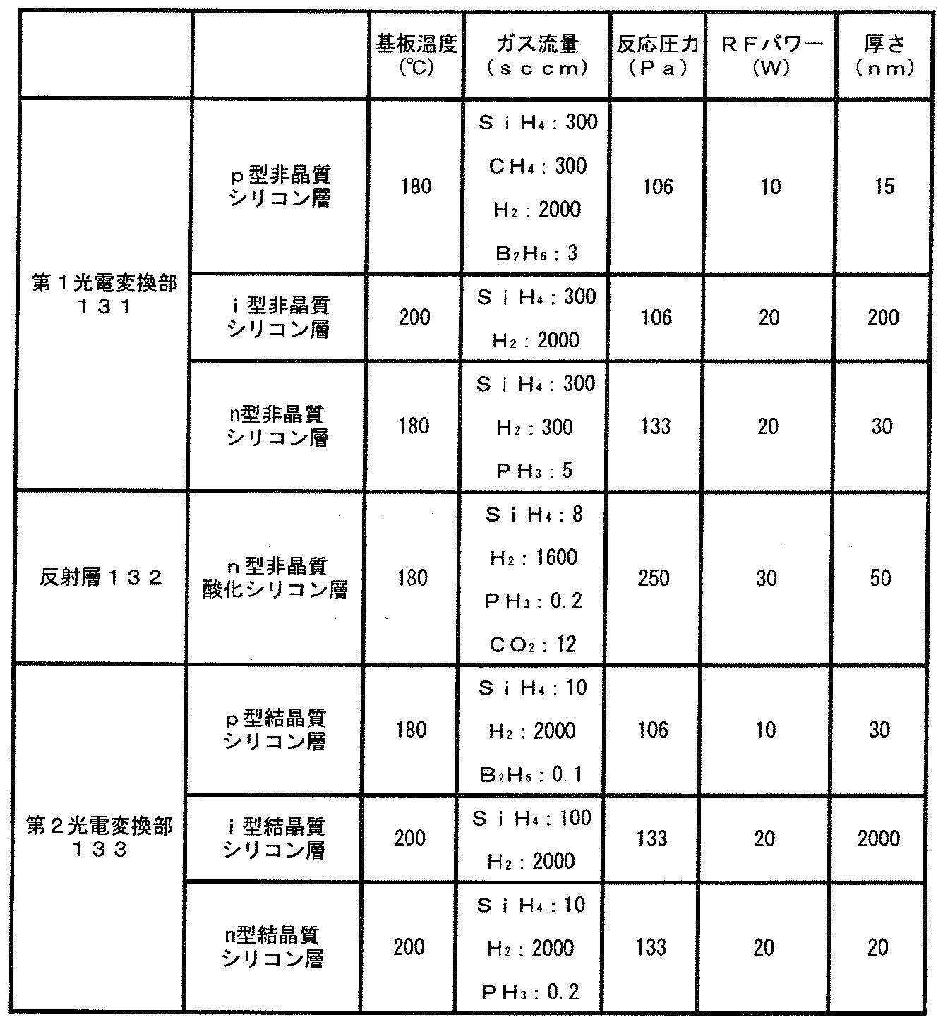
以上により、本比較例では、第1光電変換部131と第2光電変換部133との間に、SiO層により構成される反射層132を有する太陽電池20を形成した。
〈特性評価〉
実施例1、実施例2、実施例3および比較例に係る太陽電池について、開放電圧、短絡電流、曲線因子および発電効率の各特性値の比較を行った。比較結果を表5に示す。尚、表5においては、比較例における各特性値を1.00として規格化して表している。
実施例1、実施例2、実施例3および比較例に係る太陽電池について、開放電圧、短絡電流、曲線因子および発電効率の各特性値の比較を行った。比較結果を表5に示す。尚、表5においては、比較例における各特性値を1.00として規格化して表している。
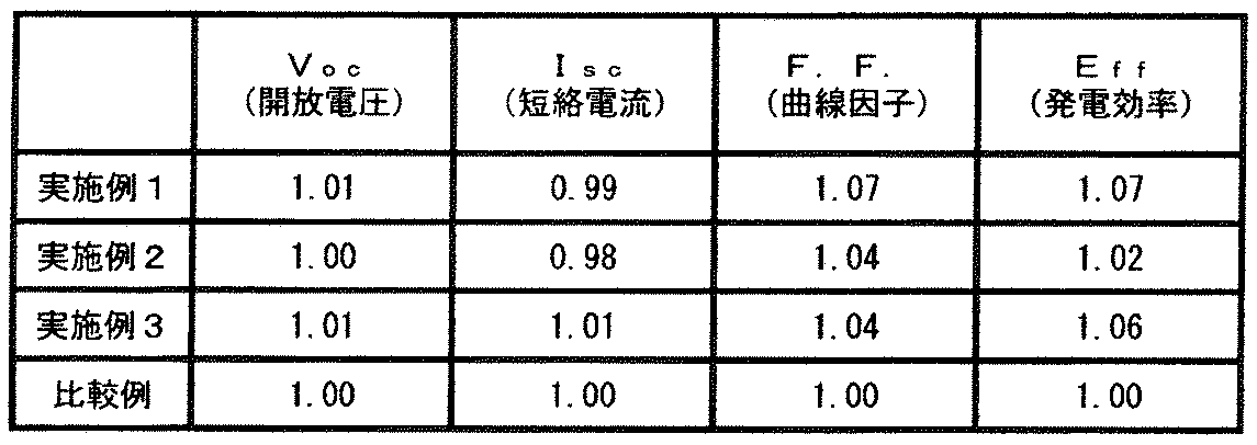
表5に示すように、実施例1、実施例2および実施例3では、曲線因子については比較例よりも増加し、発電効率が比較例よりも高くなることが確認された。
曲線因子については、実施例1、実施例2および実施例3に係る太陽電池10では、SiO層(中間層32b)と第1光電変換部31との間に第1層(32a)、もしくはSiO層(中間層32b)と第2光電変換部33との間に第2層(32c)の少なくとも一方を配置することにより増加させることが確認できた。これは、SiO層(中間層32b)と第1光電変換部31、もしくはSiO層(中間層32b)と第2光電変換部33の界面におけるコンタクト抵抗を、第1層(32a)や第2層(32c)を配置することにより小さくして、太陽電池10におけるシリーズ抵抗値を低下させることができたためと考えられる。
従って、曲線因子の改善により、いずれの実施例でもより多くの電力を取り出すことが可能となり、実施例1および実施例2では比較例に比べて短絡電流が小さくなってしまったものの、比較例よりも発電効率を向上させることができることが確認された。
なお、上記の第1実施形態に係る実施例1、実施例2および実施例3と、比較例を作成し、特性評価を行ったが、第2実施形態においては特性評価を行わなかった。しかしながら、第1実施形態と同じように(2)、(3)、(6)、(7)および(8)の効果を得ることができため、第2実施形態についても同様に、比較例に比べて良好な特性が得られると考えられる。
図2に示す第2実施形態に係る実施例は、反射層32を除き、実施例1と同様の構成とすればよい。実施例1同様、第1光電変換部31まで作成した後、第1光電変換部31上に、プラズマCVD法を用いることにより、反射層32を形成することができる。具体的には、SiO層(中間層32b)およびn型微結晶シリコン層(第2層32d)を第1光電変換部31上に順次積層することによって、2層構造を有する反射層32を形成することができる。
SiO層(中間層32b)とn型微結晶シリコン層(第2層32d)は、第1実施例のSiO層(中間層32b)、n型微結晶シリコン層(n型結晶質シリコン層33c)と同様にして形成すればよく、第1光電変換部31、反射層32および第2光電変換部33は表6に示す形成条件を用いることにより形成することができる。

以上により、第1光電変換部31と第2光電変換部33との間に、中間層32bとn型結晶質シリコン層32dを有する太陽電池10を形成することができる。
1,11…基板
2,12…受光面電極層
3…積層体
31,131…第1光電変換部
32,132…反射層
33,133…第2光電変換部
4,14…裏面電極層
10,20…太陽電池
2,12…受光面電極層
3…積層体
31,131…第1光電変換部
32,132…反射層
33,133…第2光電変換部
4,14…裏面電極層
10,20…太陽電池
本発明は、太陽電池に利用可能である。
Claims (8)
- 受光面電極層と、
前記受光面電極層上に積層された第1光電変換部と、
前記第1光電変換部上に積層され、SiO層とシリコン層とを有する反射層と、
前記反射層上に積層された第2光電変換部と、
前記第2光電変換部上に積層された裏面電極層と、
を含むことを特徴とする太陽電池。 - 前記SiO層は、非晶質であることを特徴とする請求項1に記載の太陽電池。
- 前記シリコン層は、結晶質シリコンであることを特徴とする請求項1に記載の太陽電池。
- 前記SiO層は、550nmの波長の光に対する屈折率が2.4未満であることを特徴とする請求項1に記載の太陽電池。
- 前記第2光電変換素子は、結晶質であることを特徴とする請求項1に記載の太陽電池。
- 前記第1光電変換素子は、非晶質であることを特徴とする請求項1に記載の太陽電池。
- 前記シリコン層は、真性シリコンであることを特徴とする請求項1に記載の太陽電池。
- 前記シリコン層は、一導電型シリコンであることを特徴とする請求項1に記載の太陽電池。
Priority Applications (2)
| Application Number | Priority Date | Filing Date | Title |
|---|---|---|---|
| CN2011800100678A CN102763224A (zh) | 2010-02-26 | 2011-01-28 | 太阳能电池 |
| US13/585,497 US20120305062A1 (en) | 2010-02-26 | 2012-08-14 | Solar cell |
Applications Claiming Priority (4)
| Application Number | Priority Date | Filing Date | Title |
|---|---|---|---|
| JP2010041482 | 2010-02-26 | ||
| JP2010-041482 | 2010-02-26 | ||
| JP2010-144866 | 2010-06-25 | ||
| JP2010144866A JP2011199235A (ja) | 2010-02-26 | 2010-06-25 | 太陽電池 |
Related Child Applications (1)
| Application Number | Title | Priority Date | Filing Date |
|---|---|---|---|
| US13/585,497 Continuation US20120305062A1 (en) | 2010-02-26 | 2012-08-14 | Solar cell |
Publications (1)
| Publication Number | Publication Date |
|---|---|
| WO2011105170A1 true WO2011105170A1 (ja) | 2011-09-01 |
Family
ID=44506591
Family Applications (1)
| Application Number | Title | Priority Date | Filing Date |
|---|---|---|---|
| PCT/JP2011/051781 Ceased WO2011105170A1 (ja) | 2010-02-26 | 2011-01-28 | 太陽電池 |
Country Status (4)
| Country | Link |
|---|---|
| US (1) | US20120305062A1 (ja) |
| JP (1) | JP2011199235A (ja) |
| CN (1) | CN102763224A (ja) |
| WO (1) | WO2011105170A1 (ja) |
Cited By (2)
| Publication number | Priority date | Publication date | Assignee | Title |
|---|---|---|---|---|
| WO2012099198A1 (ja) * | 2011-01-21 | 2012-07-26 | 三洋電機株式会社 | 太陽電池 |
| WO2013102576A1 (en) * | 2012-01-04 | 2013-07-11 | Tel Solar Ag | Intermediate reflection structure in thin film solar cells |
Families Citing this family (2)
| Publication number | Priority date | Publication date | Assignee | Title |
|---|---|---|---|---|
| KR101292061B1 (ko) * | 2010-12-21 | 2013-08-01 | 엘지전자 주식회사 | 박막 태양전지 |
| CN103066153A (zh) * | 2012-12-28 | 2013-04-24 | 福建铂阳精工设备有限公司 | 硅基薄膜叠层太阳能电池及其制造方法 |
Citations (3)
| Publication number | Priority date | Publication date | Assignee | Title |
|---|---|---|---|---|
| JP2001308354A (ja) * | 2000-04-24 | 2001-11-02 | Sharp Corp | 積層型太陽電池 |
| WO2005011001A1 (ja) * | 2003-07-24 | 2005-02-03 | Kaneka Corporation | 積層型光電変換装置 |
| JP2006319068A (ja) * | 2005-05-11 | 2006-11-24 | Kaneka Corp | 多接合型シリコン系薄膜光電変換装置、及びその製造方法 |
Family Cites Families (3)
| Publication number | Priority date | Publication date | Assignee | Title |
|---|---|---|---|---|
| JP4158267B2 (ja) * | 1999-03-15 | 2008-10-01 | 富士電機ホールディングス株式会社 | 非単結晶太陽電池 |
| US7671271B2 (en) * | 2006-03-08 | 2010-03-02 | National Science And Technology Dev. Agency | Thin film solar cell and its fabrication process |
| US8203071B2 (en) * | 2007-01-18 | 2012-06-19 | Applied Materials, Inc. | Multi-junction solar cells and methods and apparatuses for forming the same |
-
2010
- 2010-06-25 JP JP2010144866A patent/JP2011199235A/ja active Pending
-
2011
- 2011-01-28 WO PCT/JP2011/051781 patent/WO2011105170A1/ja not_active Ceased
- 2011-01-28 CN CN2011800100678A patent/CN102763224A/zh active Pending
-
2012
- 2012-08-14 US US13/585,497 patent/US20120305062A1/en not_active Abandoned
Patent Citations (3)
| Publication number | Priority date | Publication date | Assignee | Title |
|---|---|---|---|---|
| JP2001308354A (ja) * | 2000-04-24 | 2001-11-02 | Sharp Corp | 積層型太陽電池 |
| WO2005011001A1 (ja) * | 2003-07-24 | 2005-02-03 | Kaneka Corporation | 積層型光電変換装置 |
| JP2006319068A (ja) * | 2005-05-11 | 2006-11-24 | Kaneka Corp | 多接合型シリコン系薄膜光電変換装置、及びその製造方法 |
Cited By (2)
| Publication number | Priority date | Publication date | Assignee | Title |
|---|---|---|---|---|
| WO2012099198A1 (ja) * | 2011-01-21 | 2012-07-26 | 三洋電機株式会社 | 太陽電池 |
| WO2013102576A1 (en) * | 2012-01-04 | 2013-07-11 | Tel Solar Ag | Intermediate reflection structure in thin film solar cells |
Also Published As
| Publication number | Publication date |
|---|---|
| JP2011199235A (ja) | 2011-10-06 |
| US20120305062A1 (en) | 2012-12-06 |
| CN102763224A (zh) | 2012-10-31 |
Similar Documents
| Publication | Publication Date | Title |
|---|---|---|
| JP4940309B2 (ja) | 太陽電池 | |
| KR101292061B1 (ko) | 박막 태양전지 | |
| JP5156379B2 (ja) | シリコン系薄膜光電変換装置、及びその製造方法 | |
| JP2009231505A (ja) | 太陽電池 | |
| JP2008270562A (ja) | 多接合型太陽電池 | |
| US20120097227A1 (en) | Solar cells | |
| JP5291633B2 (ja) | シリコン系薄膜光電変換装置およびその製造方法 | |
| JP2011199235A (ja) | 太陽電池 | |
| JP2009158288A (ja) | 透明導電膜及び透明導電膜を用いた太陽電池 | |
| CN101325225A (zh) | 一种提高晶硅太阳电池短波响应的发射极结构 | |
| JP2007305826A (ja) | シリコン系薄膜太陽電池 | |
| US20110220177A1 (en) | Tandem photovoltaic device with dual function semiconductor layer | |
| KR101784439B1 (ko) | 박막 태양전지 | |
| JPWO2005109526A1 (ja) | 薄膜光電変換装置 | |
| JPWO2006006359A1 (ja) | 薄膜光電変換装置 | |
| WO2011105171A1 (ja) | 太陽電池およびその製造方法 | |
| JP5371284B2 (ja) | 薄膜光電変換装置 | |
| KR20110090316A (ko) | 태양전지 | |
| US20140130861A1 (en) | Solar cell | |
| KR20100086597A (ko) | 광기전력 장치 | |
| JP2011216586A (ja) | 積層型光電変換装置および積層型光電変換装置の製造方法 | |
| JP2014063769A (ja) | 太陽電池 | |
| JP2013008866A (ja) | 薄膜光電変換装置 | |
| JPWO2005088734A1 (ja) | 映像投射装置 | |
| JPWO2005088734A6 (ja) | 薄膜光電変換装置 |
Legal Events
| Date | Code | Title | Description |
|---|---|---|---|
| WWE | Wipo information: entry into national phase |
Ref document number: 201180010067.8 Country of ref document: CN |
|
| 121 | Ep: the epo has been informed by wipo that ep was designated in this application |
Ref document number: 11747134 Country of ref document: EP Kind code of ref document: A1 |
|
| NENP | Non-entry into the national phase |
Ref country code: DE |
|
| 122 | Ep: pct application non-entry in european phase |
Ref document number: 11747134 Country of ref document: EP Kind code of ref document: A1 |