WO2011105152A1 - ペリレンテトラカルボン酸ジイミド化合物を含有してなる有機半導体材料、及び有機半導体素子 - Google Patents
ペリレンテトラカルボン酸ジイミド化合物を含有してなる有機半導体材料、及び有機半導体素子 Download PDFInfo
- Publication number
- WO2011105152A1 WO2011105152A1 PCT/JP2011/051324 JP2011051324W WO2011105152A1 WO 2011105152 A1 WO2011105152 A1 WO 2011105152A1 JP 2011051324 W JP2011051324 W JP 2011051324W WO 2011105152 A1 WO2011105152 A1 WO 2011105152A1
- Authority
- WO
- WIPO (PCT)
- Prior art keywords
- organic semiconductor
- group
- semiconductor material
- organic
- compound
- Prior art date
- Legal status (The legal status is an assumption and is not a legal conclusion. Google has not performed a legal analysis and makes no representation as to the accuracy of the status listed.)
- Ceased
Links
Images




Classifications
-
- C—CHEMISTRY; METALLURGY
- C07—ORGANIC CHEMISTRY
- C07D—HETEROCYCLIC COMPOUNDS
- C07D471/00—Heterocyclic compounds containing nitrogen atoms as the only ring hetero atoms in the condensed system, at least one ring being a six-membered ring with one nitrogen atom, not provided for by groups C07D451/00 - C07D463/00
- C07D471/02—Heterocyclic compounds containing nitrogen atoms as the only ring hetero atoms in the condensed system, at least one ring being a six-membered ring with one nitrogen atom, not provided for by groups C07D451/00 - C07D463/00 in which the condensed system contains two hetero rings
- C07D471/04—Ortho-condensed systems
-
- H—ELECTRICITY
- H10—SEMICONDUCTOR DEVICES; ELECTRIC SOLID-STATE DEVICES NOT OTHERWISE PROVIDED FOR
- H10K—ORGANIC ELECTRIC SOLID-STATE DEVICES
- H10K85/00—Organic materials used in the body or electrodes of devices covered by this subclass
- H10K85/60—Organic compounds having low molecular weight
- H10K85/615—Polycyclic condensed aromatic hydrocarbons, e.g. anthracene
- H10K85/621—Aromatic anhydride or imide compounds, e.g. perylene tetra-carboxylic dianhydride or perylene tetracarboxylic di-imide
-
- H—ELECTRICITY
- H10—SEMICONDUCTOR DEVICES; ELECTRIC SOLID-STATE DEVICES NOT OTHERWISE PROVIDED FOR
- H10K—ORGANIC ELECTRIC SOLID-STATE DEVICES
- H10K10/00—Organic devices specially adapted for rectifying, amplifying, oscillating or switching; Organic capacitors or resistors having potential barriers
- H10K10/40—Organic transistors
- H10K10/46—Field-effect transistors, e.g. organic thin-film transistors [OTFT]
- H10K10/462—Insulated gate field-effect transistors [IGFETs]
- H10K10/484—Insulated gate field-effect transistors [IGFETs] characterised by the channel regions
Definitions
- the present invention relates to an organic semiconductor material containing a perylene tetracarboxylic acid diimide compound having a specific structure.
- the organic semiconductor material of the present invention is particularly suitable for forming an organic semiconductor layer in an organic thin film transistor (OFET) element.
- OFET organic thin film transistor
- inorganic compounds have been used in semiconductor elements such as organic electroluminescent elements, photoelectric conversion elements, and organic thin film transistor (OFET) elements used in electronic devices.
- semiconductor elements such as organic electroluminescent elements, photoelectric conversion elements, and organic thin film transistor (OFET) elements used in electronic devices.
- OFET organic thin film transistor
- a semiconductor using an inorganic compound has a problem in that the manufacturing process is expensive, and it is difficult to increase the area and the environmental load is large.
- Materials used for OFETs are required to have high carrier mobility (higher performance of the device) and excellent solubility (ease of coating process), but there is a problem that it is difficult to combine both.
- Patent Documents 1 to 3 disclose perylenetetracarboxylic acid diimide derivatives.
- Patent Documents 4 to 7 disclose perylenetetracarboxylic acid diimide compounds having a branched alkyl chain.
- an object of the present invention is to provide an organic semiconductor material that has excellent solubility and can exhibit high carrier mobility, and an organic semiconductor layer and an organic semiconductor element using the same.
- a perylenetetracarboxylic acid diimide compound having a specific structure has excellent solubility, and an organic semiconductor material containing the perylenetetracarboxylic acid diimide compound is It was found to be suitable for the coating process.
- the present inventors have found that the organic semiconductor material exhibits high carrier mobility, and have found that the object can be solved by producing an organic semiconductor element using the organic semiconductor material.
- the present invention has been made on the basis of the above knowledge, and provides an organic semiconductor material containing at least one perylenecarboxylic acid diimide compound represented by the following general formula (I).
- the present invention also provides an organic semiconductor layer formed by forming the organic semiconductor material.
- the present invention also provides an organic semiconductor element having at least one organic semiconductor layer.
- the present invention it is possible to provide an organic semiconductor material that has excellent solubility and can exhibit high carrier mobility.
- the coating process in semiconductor manufacturing becomes easy due to excellent solubility, and high performance of the element can be realized due to high carrier mobility.
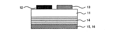
- FIG. 2 is a cross-sectional view showing a configuration example of the organic semiconductor element of the present invention (an organic thin film transistor element manufactured in an example in a modification of the bottom gate-top contact type in FIG. 1A).
- the perylenetetracarboxylic acid diimide compound used in the organic semiconductor material of the present invention is a compound represented by the above general formula (I), has an unsubstituted perylene skeleton, and is excellent in solubility.
- R 1 and R 1 ′ may be the same or different from each other.
- the unsubstituted alkyl group having 1 to 30 carbon atoms represented by R 1 and R 1 ′ in the general formula (I) may be a linear alkyl group, a branched alkyl group, or a cyclic alkyl group.
- unsubstituted alkyl group examples include methyl, ethyl, propyl, isopropyl, butyl, s-butyl, t-butyl, isobutyl, amyl, isoamyl, t-amyl, hexyl, heptyl, isoheptyl, t-heptyl, n -Octyl, isooctyl, t-octyl, n-nonyl, n-decyl, n-dodecyl, n-tridecyl, n-tetradecyl, n-pentadecyl, n-hexadecyl, n-heptadecyl, n-octadecyl, 1-ethylhexyl, 2-ethylhexyl, 3-ethylhexyl, 1-butyloctyl,
- Examples of the substituted alkyl group having 1 to 30 carbon atoms represented by R 1 and R 1 ′ in the general formula (I) include those obtained by substituting the unsubstituted alkyl group.
- Examples of the substituent for substituting the unsubstituted alkyl group include methoxy, ethoxy, propoxy, isopropoxy, butyloxy, sec-butoxy, tert-butoxy, isobutoxy, amyloxy, isoamyloxy, tert-amyloxy, hexyloxy, cyclohexyloxy, Alkoxy groups such as heptyloxy, isoheptyloxy, tertiary heptyloxy, n-octyloxy, isooctyloxy, tertiary octyloxy, 2-ethylhexyloxy, nonyloxy, decyloxy; methylthio, ethylthio, propylthio
- the number of carbon atoms of the entire group represented by R 1, R 1 'including the substituent is assumed to satisfy the range of 30 or less.
- the substituted alkyl group also preferably has a branched structure.
- R 1 is an alkyl group represented by any one of the following general formulas (II) to (IV)
- R 1 ′ is A compound that is an alkyl group represented by any one of formulas (II ′ ) to (IV ′ ) is preferred.
- R a and R b in the following general formulas (II) to (IV) and R a ′ and R b ′ in the following general formulas (II ′ ) to (IV ′ ) have no substituent, It is more preferable because the raw materials are easily available.
- those alkyl groups R 1 and / or R 1 ' is substituted by one or more fluorine atoms in the general formula (I) has high stability in the atmosphere of the element when the organic semiconductor device Therefore, it is preferable.
- a compound having 10 to 30, particularly 10 to 25, carbon atoms of R 1 and R 1 ′ in the general formula (I) is preferable because it has particularly excellent carrier mobility when an organic semiconductor element is formed.
- those in which R 1 and R 1 ′ in the above general formula (I) are unsubstituted alkyl groups are preferred from the viewpoint of improving crystallinity and increasing intermolecular interaction.
- perylenetetracarboxylic acid diimide compound used in the present invention represented by the above general formula (I) include the following compound Nos. 1-No. 26, but is not limited to these compounds.
- any of the perylenetetracarboxylic acid diimide compounds represented by the above general formula (I) is not limited to the production method, and can be obtained by a method using a known general reaction. For example, it can be produced by a reaction of perylenetetracarboxylic dianhydride and an amine as shown in the following reaction route.
- the organic semiconductor material of the present invention may contain at least one perylenetetracarboxylic acid diimide compound. That is, the organic semiconductor material of the present invention may consist of only one or two or more of the above-mentioned perylenetetracarboxylic acid diimide compounds, or in addition to the above perylenetetracarboxylic acid diimide compound, one or two of them as necessary. You may contain a seed
- the solvent examples include, but are not limited to, water, alcohol solvents, diol solvents, ketone solvents, ester solvents, ether solvents, aliphatic or alicyclic hydrocarbon solvents, and aromatic hydrocarbon solvents.
- examples thereof include a solvent, a hydrocarbon solvent having a cyano group, a halogenated hydrocarbon solvent, and other solvents.
- alcohol solvent examples include methanol, ethanol, propanol, isopropanol, 1-butanol, isobutanol, 2-butanol, tertiary butanol, pentanol, isopentanol, 2-pentanol, neopentanol, and third pentanol.
- diol solvent examples include ethylene glycol, propylene glycol, 1,2-butanediol, 1,3-butanediol, 1,4-butanediol, 1,5-pentanediol, neopentyl glycol, isoprene glycol (3- Methyl-1,3-butanediol), 1,2-hexanediol, 1,6-hexanediol, 3-methyl-1,5-pentanediol, 1,2-octanediol, octanediol (2-ethyl-1) , 3-hexanediol), 2-butyl-2-ethyl-1,3-propanediol, 2,5-dimethyl-2,5-hexanediol, 1,2-cyclohexanediol, 1,4-cyclohexanediol, 1 , 4-cyclohexane
- ketone solvents examples include acetone, ethyl methyl ketone, methyl isopropyl ketone, methyl butyl ketone, methyl isobutyl ketone, methyl amyl ketone, methyl hexyl ketone, ethyl butyl ketone, diethyl ketone, dipropyl ketone, diisobutyl ketone, and methyl amyl ketone. , Cyclohexanone, methylcyclohexanone and the like.
- ester solvents examples include methyl formate, ethyl formate, methyl acetate, ethyl acetate, isopropyl acetate, butyl acetate, isobutyl acetate, 2 butyl acetate, 3 butyl acetate, amyl acetate, isoamyl acetate, 3 amyl acetate, acetic acid Phenyl, methyl propionate, ethyl propionate, isopropyl propionate, butyl propionate, isobutyl propionate, sec-butyl propionate, tert-butyl propionate, amyl propionate, isoamyl propionate, tertiary amyl propionate, propionic acid Phenyl, methyl 2-ethylhexanoate, ethyl 2-ethylhexanoate, propyl 2-ethylhexanoate, isopropyl
- ether solvent examples include tetrahydrofuran, tetrahydropyran, morpholine, ethylene glycol dimethyl ether, diethylene glycol dimethyl ether, dipropylene glycol dimethyl ether, triethylene glycol dimethyl ether, dibutyl ether, diethyl ether, dioxane and the like.
- Examples of the aliphatic or alicyclic hydrocarbon solvents include pentane, hexane, cyclohexane, methylcyclohexane, dimethylcyclohexane, ethylcyclohexane, heptane, octane, decalin, solvent naphtha, turpentine oil, D-limonene, pinene, mineral spirit, Examples include Swazol # 310 (Cosmo Matsuyama Oil Co., Ltd., Solvesso # 100 (Exxon Chemical Co., Ltd.)).
- aromatic hydrocarbon solvent examples include benzene, toluene, ethylbenzene, xylene, mesitylene, diethylbenzene, cumene, isobutylbenzene, cymene, tetralin and the like.
- hydrocarbon solvent having a cyano group examples include acetonitrile, 1-cyanopropane, 1-cyanobutane, 1-cyanohexane, cyanocyclohexane, cyanobenzene, 1,3-dicyanopropane, 1,4-dicyanobutane, 1,6 -Dicyanohexane, 1,4-dicyanocyclohexane, 1,4-dicyanobenzene and the like.
- halogenated hydrocarbon solvent examples include carbon tetrachloride, chloroform, dichloromethane, trichloroethylene, chlorobenzene, dichlorobenzene, and trichlorobenzene.
- organic solvents examples include N-methyl-2-pyrrolidone, dimethyl sulfoxide, dimethylformamide, aniline, triethylamine, pyridine, and carbon disulfide.
- preferable solvents include chloroform, dichloromethane, toluene, xylene, mesitylene, tetrahydrofuran, tetrahydropyran, chlorobenzene, dichlorobenzene, trichlorobenzene, and the like.
- the content is not particularly limited as long as it does not hinder the formation of an organic semiconductor layer using the organic semiconductor material. It can be suitably selected from the range of 100 parts by mass or more with respect to 100 parts by mass of the perylenecarboxylic acid diimide compound represented by the formula (I), and is preferably selected from the range of 500 to 1000000 parts by mass.
- the perylene carboxylic acid diimide compound has high solubility, an organic semiconductor material having good coating properties and high organic semiconductor layer production efficiency can be obtained even if the solvent content is relatively small. it can.
- the content of the solvent is preferably 100 to 100,000 parts by mass, more preferably 7000 to 20000 parts by mass with respect to 100 parts by mass of the perylenecarboxylic acid diimide compound represented by the general formula (I). It is desirable to select from a range.
- a component that can be used for forming an organic semiconductor layer in an organic semiconductor element can be used without any particular limitation.
- the optional component include metal oxides.
- these optional components are contained, there is no particular limitation, but from the viewpoint of not impairing the function of the organic semiconductor layer, it is 30 with respect to 100 parts by mass of the perylenecarboxylic acid diimide compound represented by the general formula (I). It is preferable to make it the range below a mass part.
- the organic semiconductor material of the present invention is useful for forming an organic semiconductor layer in a semiconductor element such as an organic electroluminescence element, a photoelectric conversion element, or an organic thin film transistor (OFET) element.
- a semiconductor element such as an organic electroluminescence element, a photoelectric conversion element, or an organic thin film transistor (OFET) element.
- the organic semiconductor layer of the present invention is a thin film formed by forming the organic semiconductor material of the present invention.
- the organic semiconductor layer of the present invention can be the same as the conventional organic semiconductor layer except that the organic semiconductor material of the present invention is used for forming the organic semiconductor layer.
- the organic semiconductor layer of the present invention is usually formed on a support.
- the organic semiconductor layer of the present invention may remain formed on the support, or may optionally be a single layer of the organic semiconductor layer by removing the support.
- the organic-semiconductor layer of this invention is a layer which passed the process which removes a solvent.
- Examples of the method for producing the organic semiconductor layer of the present invention include vapor deposition, physical vapor deposition (PVD), chemical vapor deposition (CVD), atomic layer deposition (ALD), and atomic layer epitaxy (ALE). ), Dry processes such as molecular beam epitaxy (MBE), vapor phase epitaxy (VPE), sputtering, plasma polymerization, etc .; dip coating, casting, air knife coating, curtain coating, roller coating, wire Examples thereof include a method of forming a coating film on a support by a wet process such as a bar coating method, a gravure coating method, a spin coating method, an LB method, a printing method, an ink jet method or an extrusion coating method.
- PVD physical vapor deposition
- CVD chemical vapor deposition
- ALD atomic layer deposition
- ALE atomic layer epitaxy
- Dry processes such as molecular beam epitaxy (MBE), vapor phase epitaxy (VPE), sputtering, plasma
- a spin coating method, a casting method, a dip coating method, an ink jet method, a printing method, and the like are preferable because an organic semiconductor layer can be easily produced.
- the perylenecarboxylic acid diimide compound represented by the general formula (I) itself or the organic semiconductor material of the present invention in the form of a solution obtained by dissolving or dispersing the compound in the solvent is appropriately used.
- the organic semiconductor material of the present invention in the form of the solution is used.
- the film thickness of the organic semiconductor layer of the present invention is not particularly limited, but is generally 1 nm to 100 ⁇ m, more preferably 1 nm to 500 nm. If the film thickness is smaller than 1 nm, defects are likely to occur in the film, and if it is larger than 100 ⁇ m, the leakage current increases, which is not preferable.
- the organic semiconductor layer of the present invention may be doped by a conventional method, and a dopant may be introduced during or after the formation of the organic semiconductor layer.
- the dopant examples include donor dopants such as alkali metals, alkaline earth metals, rare earth metals, metal oxides, ammonium ions, and phosphonium ions, and acceptor dopants such as halogen compounds, transition metal compounds, and electrolyte anions.
- donor dopants such as alkali metals, alkaline earth metals, rare earth metals, metal oxides, ammonium ions, and phosphonium ions
- acceptor dopants such as halogen compounds, transition metal compounds, and electrolyte anions.
- the support is not particularly limited, and examples thereof include glass, a resin substrate, quartz, single crystal silicon, polycrystalline silicon, and amorphous silicon.
- the organic semiconductor element of the present invention is not particularly limited as long as it has at least one organic semiconductor layer of the present invention. Except for this point, the organic semiconductor element can be the same as the conventional organic semiconductor element.
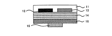
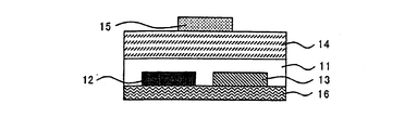
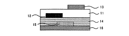
- the structural example of the organic-semiconductor element of this invention is shown as sectional drawing in FIG.1 and FIG.2.
- FIG. 1A shows a bottom gate-top contact type
- FIG. 1B shows a bottom gate-bottom contact type
- FIGS. 1C and 1D show a top gate-bottom contact type
- 1 (e) and (f) represent a bottom gate-top & bottom contact type
- FIG. 1 (g) represents a vertical electrostatic induction transistor (SIT).
- FIG. 2 is a modification of the bottom gate-top contact type of FIG. 1 and 2, reference numeral 11 denotes an organic semiconductor layer of the present invention.
- a noble metal material such as platinum, gold, or silver
- a metal material such as copper or aluminum
- a conductive material such as carbon
- a transparent conductive material such as ITO, tin oxide, or fluorine-doped tin oxide
- Examples thereof include a highly doped n-type doped silicon wafer and a highly doped p-type doped silicon wafer. These may be used alone or in combination.
- the thickness of the gate electrode 15 layer is not particularly limited, but is preferably 500 nm or less, and more preferably 100 nm or less.
- the insulating layer 14 various insulating films can be used. For example, silicon oxide, aluminum oxide, barium strontium titanate, barium zirconate titanate, lead zirconate titanate, lead lanthanum titanate, strontium titanate Barium titanate, barium magnesium fluoride, bismuth titanate, strontium bismuth titanate, tantalum oxide, strontium bismuth tantalate, bismuth tantalate niobate, titanium oxide, yttrium oxide, silicon nitride, aluminum nitride, and the like.
- the thickness of the insulating layer 14 is not specifically limited, It is 500 nm or less, More preferably, it is 300 nm or less.
- the insulating layer 14 is preferably a thin film, and is particularly preferably 100 nm or less.
- 12 is a drain electrode
- 13 is a source electrode
- 16 is a substrate.
- Synthesis Examples 1 to 8 are synthesis examples of the perylenetetracarboxylic acid diimide compound used for the organic semiconductor material of the present invention.
- a solution-like organic semiconductor material was prepared using the compound obtained in Synthesis Examples 1 to 8 or a comparative compound, and an organic semiconductor layer was formed using the organic semiconductor material. And the organic-semiconductor element was created and the element was evaluated.
- Step 2 19.3 g (68.0 mmol) of the tosyl compound, 57 ml of dimethylformamide, and 13.9 g (74.8 mmol) of potassium phthalimide were charged, and the temperature was raised to 120 ° C. and reacted for 3 hours. Ultrapure water and toluene were added to separate the oil and water, and the organic layer was extracted.
- magnesium sulfate was added to the organic layer that was washed and dried in the same manner and dried, followed by filtration and concentration under reduced pressure.
- the resulting residue was purified by silica gel column chromatography (developing solvent). : Hexane-ethyl acetate), a colorless transparent oily substance in the form of phthalimide was obtained in a yield of 64%.
- Step 3 10.4 g (131.0 mmol) of hydrazine monohydrate was added dropwise to a solution charged with 11.3 g (44.0 mmol) of the phthalimide compound and 220 ml of methanol. After raising the reaction temperature to 80 ° C., the reaction was allowed to proceed for 2 hours, chloroform and 10% aqueous potassium hydroxide solution were added, and the organic layer was extracted by oil-water separation. The aqueous layer was re-extracted and combined with the organic layer.
- Aqueous ammonium chloride solution, hexane and ethyl acetate were added to separate the oil and water, and the organic layer was extracted. The extract was washed with sodium chloride, dried by adding magnesium sulfate, filtered and concentrated under reduced pressure. The resulting residue was purified by silica gel column chromatography (developing solvent: hexane-ethyl acetate). ), Methyl 3-butyloctanoate (pale yellow transparent oil) was obtained in a yield of 99%.
- Step 2 Under a nitrogen atmosphere, 2.7 g (70.0 mmol) of lithium aluminum hydride and 69 ml of tetrahydrofuran were charged, and a solution of 7.5 g (35.0 mmol) of methyl 3-butyloctanoate in tetrahydrofuran (25 ml) was added dropwise. The temperature was raised to 90 ° C. and reacted for 5 hours. Sodium sulfate and tetrahydrofuran were added, and the mixture was stirred for 30 minutes. After filtration, the residue was washed with tetrahydrofuran. Magnesium sulfate was added to the combined organic layers and dried, followed by filtration and concentration under reduced pressure to obtain an alcohol form (light yellow transparent oily substance) with a yield of 99%. This alcohol was used for the next step reaction without purification.
- Step 3 7.6 g (40.0 mmol) of p-toluenesulfonyl chloride was added under ice cooling to a solution charged with 6.2 g (33.3 mmol) of the alcohol and 15 ml of pyridine, and reacted at the same temperature for 1 hour. It was. Hydrochloric acid and toluene were added to separate the oil and water, and the organic layer was extracted. The extract was washed with ultrapure water, dried by adding magnesium sulfate, filtered and concentrated under reduced pressure. The resulting residue was purified by silica gel column chromatography (developing solvent: hexane-acetic acid).
- Step 4 6.1 g (18.0 mmol) of the tosyl compound, 14 ml of dimethylformamide, and 4.0 g (21.6 mmol) of potassium phthalimide were charged, heated to 150 ° C., and reacted for 3 hours. Ultrapure water and toluene were added to separate the oil and water, and the organic layer was extracted.
- magnesium sulfate was added to the organic layer that was washed and combined in the same manner, dried, then filtered and concentrated under reduced pressure, and the resulting residue was purified by silica gel column chromatography (developing solvent). : Hexane-ethyl acetate), a colorless transparent oily substance in the form of phthalimide was obtained in a yield of 93%.
- Step 5 To a solution charged with 5.1 g (16.4 mmol) of the phthalimide compound and 80 ml of methanol, 2.5 g (49.3 mmol) of hydrazine monohydrate was added dropwise. After raising the reaction temperature to 100 ° C., the reaction was allowed to proceed for 2 hours, chloroform and 10% aqueous potassium hydroxide solution were added, and the organic layer was extracted by oil-water separation. The aqueous layer was re-extracted and combined with the organic layer. The extract was washed with 10% aqueous potassium hydroxide solution, dried by adding magnesium sulfate, filtered and concentrated under reduced pressure to give 3-butyl-octylamine.
- Step 6 1.0 g (2.6 mmol) of perylenetetracarboxylic dianhydride, 370 mg (2.0 mmol) of zinc acetate, 10.4 g (153.0 mmol) of imidazole and 3-butyl-octyl obtained in Step 5 1.2 g (6.4 mmol) of amine was charged and reacted at 160 ° C. for 2 hours.
- Step 2 Under a nitrogen atmosphere, 2.9 g (14.0 mmol) of the above ketoxime and 91 ml of toluene were charged, 9.5 ml (34 mmol) of sodium bis (2-methoxyethoxy) aluminum hydride was added dropwise, and the temperature was raised to 100 ° C. Warmed and allowed to react for 2 hours. Ultrapure water and hexane were added to separate the oil and water, and the organic layer was extracted.
- Step 3 1.0 g (2.5 mmol) of perylenetetracarboxylic dianhydride, 370 mg (2.0 mmol) of zinc acetate, 5.2 g (76.5 mmol) of imidazole and 1-hexylheptyl obtained in Step 2 1.3 g (6.4 mmol) of amine was charged and reacted at 160 ° C.
- Example 1 Compound 1 was added to 1 ml of chloroform. 1 was dissolved at a rate of 7 mg to obtain a solution-like organic semiconductor material. Using this organic semiconductor material, an organic thin film transistor (OTFT) device having the layer structure shown in FIG. 2 was produced by the following procedure. An n-type doped silicon substrate (substrate 16 and gate electrode 15) on which a 300 nm thick silicon oxide film (insulating layer 14) is formed is subjected to UV ozone treatment and then treated with hexamethyldisilazane (HMDS) to form a self-assembled film. (Hereinafter, the one formed up to the self-assembled film is referred to as a Si-treated substrate).
- HMDS hexamethyldisilazane
- Compound No. 1 was added dropwise, and the organic semiconductor layer 11 was formed to a thickness of 25 to 30 nm by spin coating.
- a patterned nickel mask was placed on the surface of the organic semiconductor layer 11, and gold was vacuum-deposited to form a drain electrode 12 and a source electrode 13 to be electrodes.
- the drain electrode 12 and the source electrode 13 have a channel width of 5 mm and a channel length of 20 ⁇ m.
- the fabricated OTFT device exhibited n-channel-enhanced operating characteristics in which the drain current increases as a positive gate voltage is applied.
- the carrier mobility charge mobility
- Vd 80 V and Vg is 0 to 80 V
- the carrier mobility and the On / Off ratio were also measured when the OTFT device was heated (annealed) at 150 ° C. for 30 minutes.
- Example 2 to 8 Compound No. 1 used in Example 1 An organic semiconductor material was prepared in the same manner as in Example 1 except that 1 was changed to the compound shown in [Table 1], and an OTFT device was prepared using the organic semiconductor material and evaluated.
- Comparative Example 1 Compound No. 1 used in Example 1 Example 1 except that 1 was changed to N, N ′-(2-ethylhexyl) -2,7-dicyano-3,4,9,10-perylenetetracarboxylic acid diimide (hereinafter also referred to as comparative compound No. 1) An OTFT device was prepared by the same method as in Example 1 and evaluated.
- Comparative Example 2 Compound No. 1 used in Example 1 Example 1 except that 1 was changed to N, N ′-(2-ethylhexyl) -2,7-difluoro-3,4,9,10-perylenetetracarboxylic acid diimide (hereinafter also referred to as comparative compound No. 2) An OTFT device was prepared by the same method as in Example 1 and evaluated.
- Comparative Example 3 Compound No. 1 used in Example 1 Example 1 except that 1 was changed to N, N ′-[(+)-dehydroabiethyl] -3,4,9,10-perylenetetracarboxylic acid diimide (hereinafter also referred to as Comparative Compound No. 3). An OTFT device was fabricated in the same manner and evaluated.
- Example 9 An organic thin film transistor (OTFT) device having the layer configuration shown in FIG. 2 was produced by the following procedure. On the Si-treated substrate, Compound No. 3 was laminated at 30 nm under a high vacuum (10 ⁇ 4 to 10 ⁇ 3 Pa) at a deposition rate of 0.02 nm / sec to form an organic semiconductor layer 11. A patterned nickel mask is overlaid on the surface of the organic semiconductor layer 11, and vacuum deposition is performed using gold, thereby forming a source electrode 13 and a drain electrode 12 to obtain an OTFT device. The source electrode 13 and the drain electrode 12 were formed with a channel width of 5 mm and a channel length of 20 ⁇ m.
- OTFT organic thin film transistor
- the fabricated OTFT device exhibited n-channel-enhanced operating characteristics in which the drain current increases as a positive gate voltage is applied.
- the charge mobility was 5.3 ⁇ 10 ⁇ 2 cm 2 / Vs, and the On / Off ratio was 10 5 .
- the value of charge mobility 1.0 * 10 ⁇ -1 > cm ⁇ 2 > / Vs and On / Off ratio 10 ⁇ 7 > was shown. .
- the organic semiconductor material containing at least one perylenecarboxylic acid diimide compound of the present invention is suitable not only for film formation by a wet process but also by a dry process such as vacuum deposition. It is obvious that the organic semiconductor element formed by any process exhibits high carrier mobility.
Landscapes
- Chemical & Material Sciences (AREA)
- Organic Chemistry (AREA)
- Physics & Mathematics (AREA)
- Spectroscopy & Molecular Physics (AREA)
- Engineering & Computer Science (AREA)
- Materials Engineering (AREA)
- Thin Film Transistor (AREA)
- Nitrogen Condensed Heterocyclic Rings (AREA)
- Organic Low-Molecular-Weight Compounds And Preparation Thereof (AREA)
- Photovoltaic Devices (AREA)
Abstract
本発明の有機半導体材料は、下記一般式(I)で表されるペリレンカルボン酸ジイミド化合物を少なくとも一種含有してなる。下記式中、R1及びR1'は水素原子、炭素原子数1~30の無置換アルキル基又は炭素原子数1~30の置換アルキル基を表し、該置換アルキル基の置換基は、アルコキシ基、アルキルチオ基、アリール基、アリールオキシ基、アリールチオ基、複素環基、アシル基、アシルオキシ基、シアノ基、ニトロ基、ビニル基、(メタ)アクリル基、エポキシ基又はハロゲン原子等である。
Description
本発明は、特定の構造を有するペリレンテトラカルボン酸ジイミド化合物を含有してなる有機半導体材料に関する。本発明の有機半導体材料は、特に有機薄膜トランジスタ(OFET)素子における有機半導体層の形成に好適なものである。
従来より、電子デバイスに使用される有機電界発光素子、光電変換素子、有機薄膜トランジスタ(OFET)素子等の半導体素子には、無機化合物が使用されてきた。しかしながら、無機化合物を用いた半導体では製造プロセスが高価であり、大面積化が難しく環境負荷が大きい等の問題もあった。
近年、有機分子で半導体に使用可能なものが見出され、安価な製造プロセス(低温での製膜化や希少元素を必要としない)、素子の軽量化、材料の多様性、大面積化・薄型化、環境負荷の低減(例えば毒性のある元素を含有しない)、高集積化等が期待され、研究が盛んになっている。
OFETに用いられる材料には、高いキャリア移動度(素子の高性能化)と優れた溶解性(塗工プロセスの容易性)が求められるが、両方を兼ね備えることは難しいという問題があった。
特許文献1~3には、ペリレンテトラカルボン酸ジイミド誘導体が開示されている。特許文献4~7には、分岐アルキル鎖を有するペリレンテトラカルボン酸ジイミド化合物が開示されている。
従って、本発明の目的は、優れた溶解性を有し、且つ高いキャリア移動度を発現できる有機半導体材料、並びにそれを用いた有機半導体層及び有機半導体素子を提供することにある。
本発明者は、鋭意検討を重ねた結果、特定の構造を有するペリレンテトラカルボン酸ジイミド化合物が優れた溶解性を有しており、該ペリレンテトラカルボン酸ジイミド化合物を含有してなる有機半導体材料は、塗工プロセスに適していることを見出した。さらに検討を進めた結果、該有機半導体材料が、高いキャリア移動度を示すことを知見し、これを用いて有機半導体素子を製造することにより、上記目的を解決し得ることを知見した。
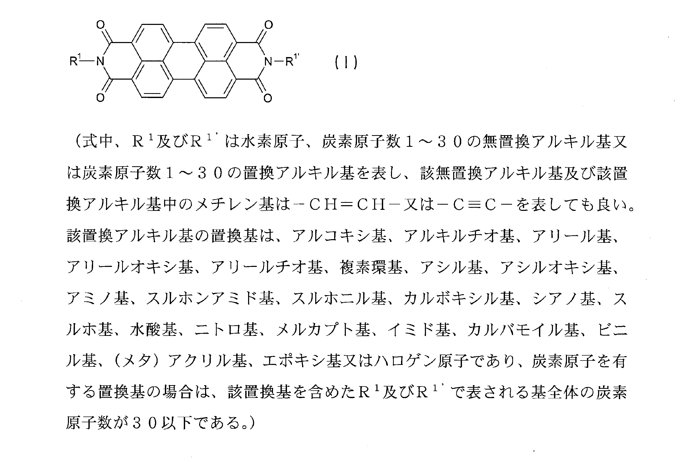
本発明は、上記知見に基づいてなされたもので、下記一般式(I)で表されるペリレンカルボン酸ジイミド化合物を少なくとも一種含有してなる有機半導体材料を提供するものである。
また、本発明は、上記有機半導体材料を製膜してなる有機半導体層を提供するものである。
また、本発明は、上記有機半導体層を少なくとも1層有する有機半導体素子を提供するものである。
本発明によれば、優れた溶解性を有し、且つ高いキャリア移動度を発現できる有機半導体材料を提供することができる。本発明の有機半導体材料を用いれば、優れた溶解性により、半導体製造における塗工プロセスが容易になり、且つ、高いキャリア移動度により、素子の高性能化を実現できる。
以下、本発明のペリレンテトラカルボン酸ジイミド化合物を少なくとも一種含有してなる有機半導体材料、有機半導体層、及び有機半導体素子について、好ましい実施形態に基づき詳細に説明する。
本発明の有機半導体材料に用いられるペリレンテトラカルボン酸ジイミド化合物は、上記一般式(I)で表される化合物であり、ペリレン骨格が無置換であり、溶解性に優れるものである。上記一般式(I)において、R1とR1'は同一でもよく、互いに異なっていてもよい。
上記一般式(I)におけるR1、R1'で表される炭素原子数1~30の無置換アルキル基は、直鎖アルキル基でも分岐アルキル基でもよく、また環状アルキル基でもよい。該無置換アルキル基の具体例としては、メチル、エチル、プロピル、イソプロピル、ブチル、s-ブチル、t-ブチル、イソブチル、アミル、イソアミル、t-アミル、ヘキシル、ヘプチル、イソヘプチル、t-ヘプチル、n-オクチル、イソオクチル、t-オクチル、n-ノニル、n-デシル、n-ドデシル、n-トリデシル、n-テトラデシル、n-ペンタデシル、n-ヘキサデシル、n-へプタデシル、n-オクタデシル、1-エチルヘキシル、2-エチルヘキシル、3-エチルヘキシル、1-ブチルオクチル、2-ブチルオクチル、3-ブチルオクチル、1-ヘキシルデシル、2-ヘキシルデシル、3-ヘキシルデシル、1-デシルテトラデシル、2-デシルテトラデシル、3-デシルテトラデシル、シクロプロピル、シクロブチル、シクロペンチル、シクロヘキシル、シクロヘプチル、シクロオクチル、シクロノニル、シクロデシル等が挙げられる。これらの中でも、1-エチルヘキシル、2-エチルヘキシル、3-エチルヘキシル、1-ブチルオクチル、2-ブチルオクチル、3-ブチルオクチル、1-ヘキシルデシル、2-ヘキシルデシル、3-ヘキシルデシル、1-デシルテトラデシル、2-デシルテトラデシル、3-デシルテトラデシル等の分岐アルキル基が好ましい。
上記一般式(I)におけるR1、R1'で表される炭素原子数1~30の置換アルキル基としては、上記無置換アルキル基を置換してなるものが挙げられる。上記無置換アルキル基を置換する置換基としては、例えばメトキシ、エトキシ、プロポキシ、イソプロポキシ、ブチルオキシ、第二ブトキシ、第三ブトキシ、イソブトキシ、アミルオキシ、イソアミルオキシ、第三アミルオキシ、ヘキシルオキシ、シクロヘキシルオキシ、ヘプチルオキシ、イソヘプチルオキシ、第三ヘプチルオキシ、n-オクチルオキシ、イソオクチルオキシ、第三オクチルオキシ、2-エチルヘキシルオキシ、ノニルオキシ、デシルオキシ等のアルコキシ基;メチルチオ、エチルチオ、プロピルチオ、イソプロピルチオ、ブチルチオ、第二ブチルチオ、第三ブチルチオ、イソブチルチオ、アミルチオ、イソアミルチオ、第三アミルチオ、ヘキシルチオ、シクロヘキシルチオ、ヘプチルチオ、イソヘプチルチオ、第三ヘプチルチオ、n-オクチルチオ、イソオクチルチオ、第三オクチルチオ、2-エチルヘキシルチオ等のアルキルチオ基;フェニル、ナフチル等のアリール基;フェノキシ、ナフチルオキシ等のアリールオキシ基;フェニルチオ、ナフチルチオ等のアリールチオ基;ピリジル、ピリミジル、ピリダジル、ピペリジル、ピラニル、ピラゾリル、トリアジル、ピロリル、キノリル、イソキノリル、イミダゾリル、ベンゾイミダゾリル、トリアゾリル、フリル、フラニル、ベンゾフラニル、チエニル、チオフェニル、ベンゾチオフェニル、チアジアゾリル、チアゾリル、ベンゾチアゾリル、オキサゾリル、ベンゾオキサゾリル、イソチアゾリル、イソオキサゾリル、インドリル、2-ピロリジノン-1-イル、2-ピペリドン-1-イル、2,4-ジオキシイミダゾリジン-3-イル、2,4-ジオキシオキサゾリジン-3-イル等の複素環基;アセチル、2-クロロアセチル、プロピオニル、オクタノイル、アクリロイル、メタクリロイル、フェニルカルボニル(ベンゾイル)、フタロイル、4-トリフルオロメチルベンゾイル、ピバロイル、サリチロイル、オキザロイル、ステアロイル、メトキシカルボニル、エトキシカルボニル、t-ブトキシカルボニル、n-オクタデシルオキシカルボニル、カルバモイル等のアシル基;アセチルオキシ、ベンゾイルオキシ等のアシルオキシ基;アミノ、エチルアミノ、ジメチルアミノ、ジエチルアミノ、ブチルアミノ、シクロペンチルアミノ、2-エチルヘキシルアミノ、ドデシルアミノ、アニリノ、クロロフェニルアミノ、トルイジノ、アニシジノ、N-メチル-アニリノ、ジフェニルアミノ,ナフチルアミノ、2-ピリジルアミノ、メトキシカルボニルアミノ、フェノキシカルボニルアミノ、アセチルアミノ、ベンゾイルアミノ、ホルミルアミノ、ピバロイルアミノ、ラウロイルアミノ、カルバモイルアミノ、N,N-ジメチルアミノカルボニルアミノ、N,N-ジエチルアミノカルボニルアミノ、モルホリノカルボニルアミノ、メトキシカルボニルアミノ、エトキシカルボニルアミノ、t-ブトキシカルボニルアミノ、n-オクタデシルオキシカルボニルアミノ、N-メチル-メトキシカルボニルアミノ、フェノキシカルボニルアミノ、スルファモイルアミノ、N,N-ジメチルアミノスルホニルアミノ、メチルスルホニルアミノ、ブチルスルホニルアミノ、フェニルスルホニルアミノ等の置換されていてもよいアミノ基;フッ素、塩素、臭素、ヨウ素等のハロゲン原子;スルホンアミド基、スルホニル基、カルボキシル基、シアノ基、スルホ基、水酸基、ニトロ基、メルカプト基、イミド基、カルバモイル基、ビニル基、アクリル基、メタクリル基、エポキシ基が挙げられ、好ましくはハロゲン原子である。尚、炭素原子を有する置換基で置換される場合は、該置換基を含めたR1、R1'で表される基全体の炭素原子数が30以下の範囲を満たすものとする。また、置換アルキル基の場合も、分岐構造を有するものであることが好ましい。
上記一般式(I)で表されるペリレンテトラカルボン酸ジイミド化合物の中でも、R1が下記一般式(II)~(IV)のいずれかで表されるアルキル基であり且つR1’が下記一般式(II')~(IV')のいずれかで表されるアルキル基である化合物が好ましい。更に、下記一般式(II)~(IV)中のRa及びRb並びに下記一般式(II')~(IV')中のRa'及びRb'が置換基を有しないものは、原料の入手が容易であるためより好ましい。
また、上記一般式(I)におけるR1及び/又はR1’が1以上のフッ素原子で置換されたアルキル基であるものは、有機半導体素子にしたときの素子の大気中における安定性が高いため好ましい。
また、上記一般式(I)におけるR1及びR1’の炭素原子数が10~30、特に10~25の化合物は、有機半導体素子にしたときのキャリア移動度にとりわけ優れるため好ましい。
また、上記一般式(I)におけるR1及びR1’が無置換アルキル基であるものは、結晶性の向上と分子間相互作用の増大の観点から好ましい。
また、上記一般式(I)におけるR1及び/又はR1’が1以上のフッ素原子で置換されたアルキル基であるものは、有機半導体素子にしたときの素子の大気中における安定性が高いため好ましい。
また、上記一般式(I)におけるR1及びR1’の炭素原子数が10~30、特に10~25の化合物は、有機半導体素子にしたときのキャリア移動度にとりわけ優れるため好ましい。
また、上記一般式(I)におけるR1及びR1’が無置換アルキル基であるものは、結晶性の向上と分子間相互作用の増大の観点から好ましい。
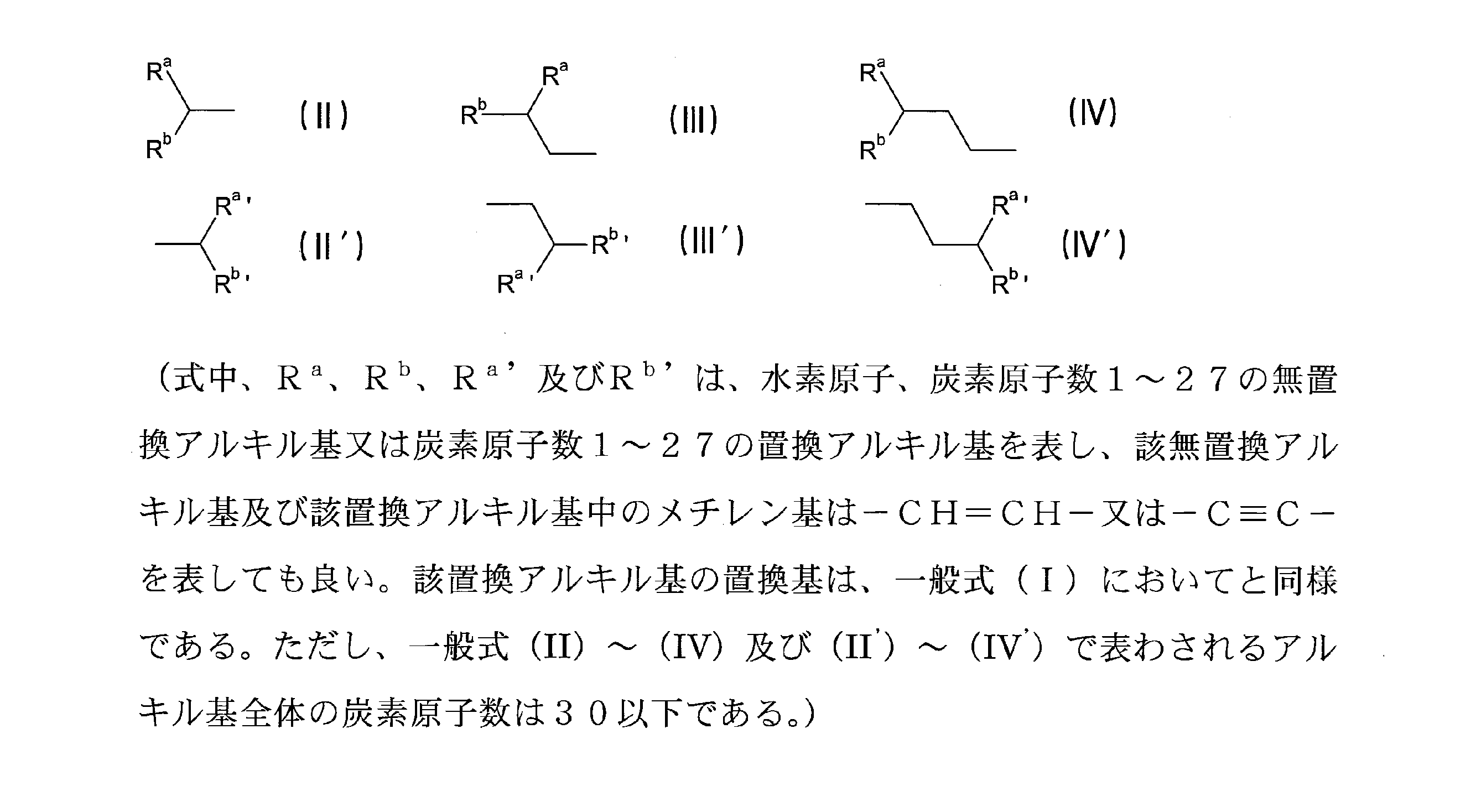
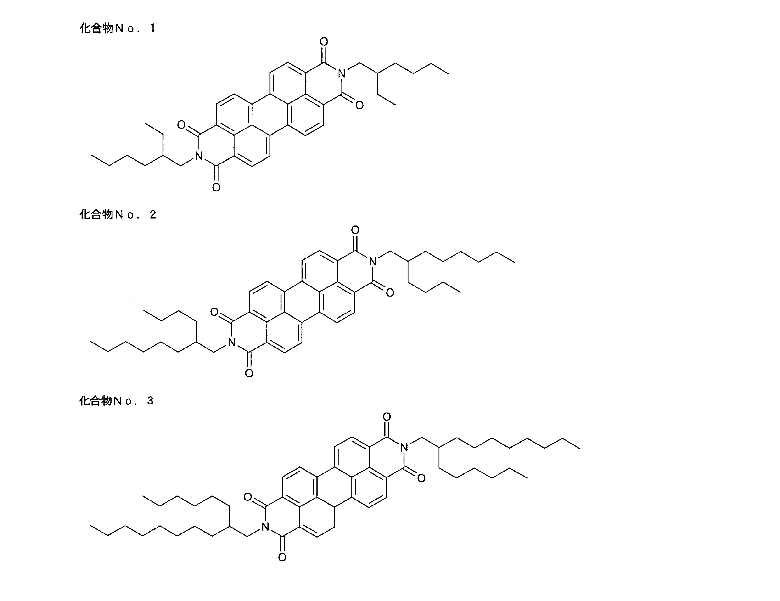
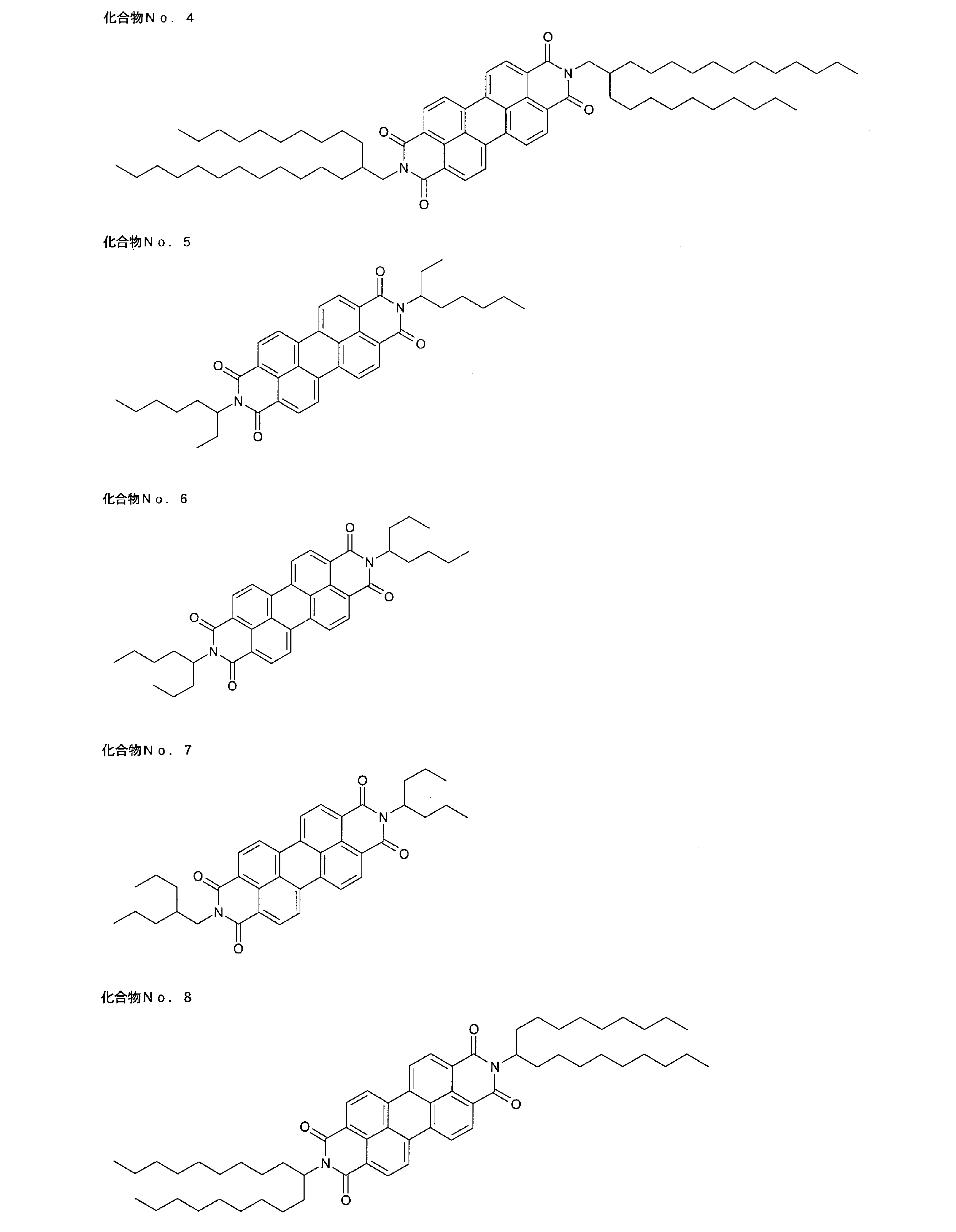
上記一般式(I)で表される、本発明に用いられるペリレンテトラカルボン酸ジイミド化合物の具体例としては、下記化合物No.1~No.26が挙げられるが、これらの化合物に制限されない。


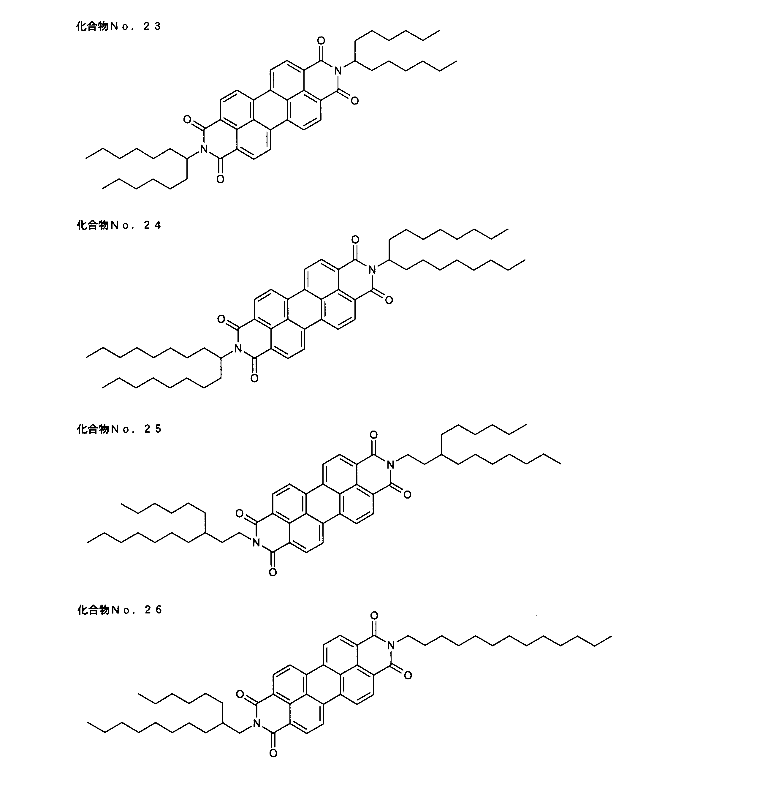
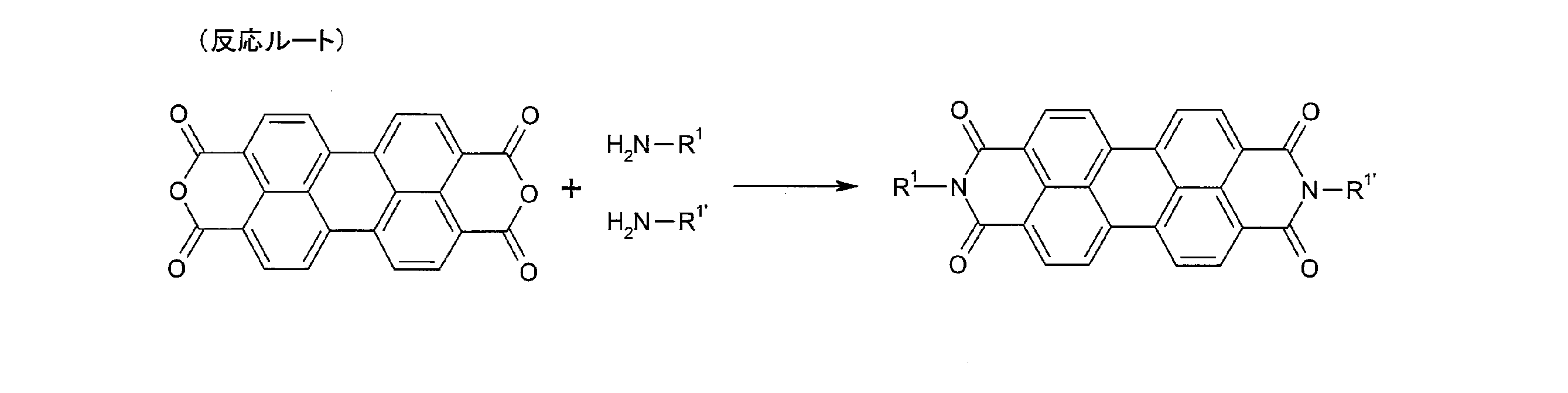
上記一般式(I)で表されるペリレンテトラカルボン酸ジイミド化合物は、何れも、その製造方法に制限されず、周知一般の反応を利用した方法で得ることができる。例えば、下記反応ルートの如く、ペリレンテトラカルボン酸二無水物とアミンとの反応で製造可能である。
本発明の有機半導体材料は、上記ペリレンテトラカルボン酸ジイミド化合物を少なくとも一種含有していれば良い。即ち、本発明の有機半導体材料は、一種又は二種以上の上記ペリレンテトラカルボン酸ジイミド化合物のみからなっていてもよいし、上記ペリレンテトラカルボン酸ジイミド化合物に加えて、必要に応じて一種又は二種以上の溶媒等を含有してもよい。
上記溶媒としては、特に制限されないが、例えば、水、アルコール系溶剤、ジオール系溶剤、ケトン系溶剤、エステル系溶剤、エーテル系溶剤、脂肪族又は脂環族炭化水素系溶剤、芳香族炭化水素系溶剤、シアノ基を有する炭化水素溶剤、ハロゲン化炭化水素系溶剤、その他の溶剤等が挙げられる。
上記アルコール系溶剤としては、メタノール、エタノール、プロパノール、イソプロパノール、1-ブタノール、イソブタノール、2-ブタノール、第3ブタノール、ペンタノール、イソペンタノール、2-ペンタノール、ネオペンタノール、第3ペンタノール、ヘキサノール、2-ヘキサノール、ヘプタノール、2-ヘプタノール、オクタノール、2―エチルヘキサノール、2-オクタノール、シクロペンタノール、シクロヘキサノール、シクロヘプタノール、メチルシクロペンタノール、メチルシクロヘキサノール、メチルシクロヘプタノール、ベンジルアルコール、エチレングリコールモノメチルエーテル、エチレングリコールモノエチルエーテル、プロピレングリコールモノメチルエーテル、プロピレングルコールモノエチルエーテル、ジエチレングルコールモノメチルエーテル、ジエチレングリコールモノエチルエーテル、トリエチレングリコールモノメチルエーテル、トリエチレングリコールモノエチルエーテル、2-(N,N-ジメチルアミノ)エタノール、3(N,N-ジメチルアミノ)プロパノール等が挙げられる。
上記ジオール系溶剤としては、エチレングリコール、プロピレングリコール、1,2-ブタンジオール、1,3-ブタンジオール、1,4-ブタンジオール、1,5-ペンタンジオール、ネオペンチルグリコール、イソプレングリコール(3-メチル-1,3-ブタンジオール)、1,2-ヘキサンジオール、1,6-ヘキサンジオール、3-メチル-1,5-ペンタンジオール、1,2-オクタンジオール、オクタンジオール(2-エチル-1,3-ヘキサンジオール)、2-ブチル-2-エチル-1,3-プロパンジオール、2,5-ジメチル-2,5-ヘキサンジオール、1,2-シクロヘキサンジオール、1,4-シクロヘキサンジオール、1,4-シクロヘキサンジメタノール等が挙げられる。
上記ケトン系溶剤としては、アセトン、エチルメチルケトン、メチルイソプロピルケトン、メチルブチルケトン、メチルイソブチルケトン、メチルアミルケトン、メチルヘキシルケトン、エチルブチルケトン、ジエチルケトン、ジプロピルケトン、ジイソブチルケトン、メチルアミルケトン、シクロヘキサノン、メチルシクロヘキサノン等が挙げられる。
上記エステル系溶剤としては、ギ酸メチル、ギ酸エチル、酢酸メチル、酢酸エチル、酢酸イソプロピル、酢酸ブチル、酢酸イソブチル、酢酸第2ブチル、酢酸第3ブチル、酢酸アミル、酢酸イソアミル、酢酸第3アミル、酢酸フェニル、プロピオン酸メチル、プロピオン酸エチル、プロピオン酸イソプロピル、プロピオン酸ブチル、プロピオン酸イソブチル、プロピオン酸第2ブチル、プロピオン酸第3ブチル、プロピオン酸アミル、プロピオン酸イソアミル、プロピオン酸第3アミル、プロピオン酸フェニル、2-エチルヘキサン酸メチル、2-エチルヘキサン酸エチル、2-エチルヘキサン酸プロピル、2-エチルヘキサン酸イソプロピル、2-エチルヘキサン酸ブチル、乳酸メチル、乳酸エチル、メトキシプロピオン酸メチル、エトキシプロピオン酸メチル、メトキシプロピオン酸エチル、エトキシプロピオン酸エチル、エチレングリコールモノメチルエーテルアセテート、ジエチレングリコールモノメチルエーテルアセテート、エチレングリコールモノエチルエーテルアセテート、エチレングリコールモノプロピルエーテルアセテート、エチレングリコールモノイソプロピルエーテルアセテート、エチレングリコールモノブチルエーテルアセテート、エチレングリコールモノ第2ブチルエーテルアセテート、エチレングリコールモノイソブチルエーテルアセテート、エチレングリコールモノ第3ブチルエーテルアセテート、プロピレングリコールモノメチルエーテルアセテート、プロピレングリコールモノエチルエーテルアセテート、プロピレングリコールモノプロピルエーテルアセテート、プロピレングリコールモノイソプロピルエーテルアセテート、プロピレングリコールモノブチルエーテルアセテート、プロピレングリコールモノ第2ブチルエーテルアセテート、プロピレングリコールモノイソブチルエーテルアセテート、プロピレングリコールモノ第3ブチルエーテルアセテート、ブチレングリコールモノメチルエーテルアセテート、ブチレングリコールモノエチルエーテルアセテート、ブチレングリコールモノプロピルエーテルアセテート、ブチレングリコールモノイソプロピルエーテルアセテート、ブチレングリコールモノブチルエーテルアセテート、ブチレングリコールモノ第2ブチルエーテルアセテート、ブチレングリコールモノイソブチルエーテルアセテート、ブチレングリコールモノ第3ブチルエーテルアセテート、アセト酢酸メチル、アセト酢酸エチル、オキソブタン酸メチル、オキソブタン酸エチル、γ-ラクトン、マロン酸ジメチル、コハク酸ジメチル、プロピレングリコールジアセテート、δ-ラクトン等が挙げられる。
上記エーテル系溶剤としては、テトラヒドロフラン、テトラヒドロピラン、モルホリン、エチレングリコールジメチルエーテル、ジエチレングリコールジメチルエーテル、ジプロピレングリコールジメチルエーテル、トリエチレングリコールジメチルエーテル、ジブチルエーテル、ジエチルエーテル、ジオキサン等が挙げられる。
上記脂肪族又は脂環族炭化水素系溶剤としては、ペンタン、ヘキサン、シクロヘキサン、メチルシクロヘキサン、ジメチルシクロヘキサン、エチルシクロヘキサン、ヘプタン、オクタン、デカリン、ソルベントナフサ、テレピン油、D-リモネン、ピネン、ミネラルスピリット、スワゾール#310(コスモ松山石油(株)、ソルベッソ#100(エクソン化学(株))等が挙げられる。
上記芳香族炭化水素系溶剤としては、ベンゼン、トルエン、エチルベンゼン、キシレン、メシチレン、ジエチルベンゼン、クメン、イソブチルベンゼン、シメン、テトラリン等が挙げられる。
上記シアノ基を有する炭化水素溶剤としては、アセトニトリル、1-シアノプロパン、1-シアノブタン、1-シアノヘキサン、シアノシクロヘキサン、シアノベンゼン、1,3-ジシアノプロパン、1,4-ジシアノブタン、1,6-ジシアノヘキサン、1,4-ジシアノシクロヘキサン、1,4-ジシアノベンゼン等が挙げられる。
上記ハロゲン化炭化水素系溶媒としては、四塩化炭素、クロロホルム、ジクロロメタン、トリクロロエチレン、クロロベンゼン、ジクロロベンゼン、トリクロロベンゼン等が挙げられる。
上記その他の有機溶剤としては、N-メチル-2-ピロリドン、ジメチルスルホキシド、ジメチルホルムアミド、アニリン、トリエチルアミン、ピリジン、2硫化炭素等が挙げられる。
これらのうちでも、好ましい溶媒としては、クロロホルム、ジクロロメタン、トルエン、キシレン、メシチレン、テトラヒドロフラン、テトラヒドロピラン、クロロベンゼン、ジクロロベンゼン、トリクロロベンゼン等が挙げられる。
本発明の有機半導体材料に上記溶媒を含有させる場合、その含有量は、該有機半導体材料を用いた有機半導体層の形成に支障が生じない限り特に制限されるものではないが、例えば、上記一般式(I)で表されるペリレンカルボン酸ジイミド化合物100質量部に対し100質量部以上の範囲から適宜選択することができ、500~1000000質量部の範囲から選択することが望ましい。しかしながら、上記ペリレンカルボン酸ジイミド化合物は溶解性が高いため、溶媒の含有量が比較的少量であっても、塗工性が良好で且つ有機半導体層の作製効率の良い有機半導体材料とすることができる。この観点からすると、上記溶媒の含有量は、上記一般式(I)で表されるペリレンカルボン酸ジイミド化合物100質量部に対し、好ましくは100~100000質量部、さらに好ましくは7000~20000質量部の範囲から選択することが望ましい。
本発明の有機半導体材料には、さらに任意成分として、有機半導体素子における有機半導体層の形成に使用可能な成分を特に制限なく使用することができる。該任意成分の例としては、金属酸化物等が挙げられる。これらの任意成分を含有させる場合、特に制限されるものではないが、有機半導体層の機能を損ねない観点から、上記一般式(I)で表されるペリレンカルボン酸ジイミド化合物100質量部に対し30質量部以下の範囲とすることが好ましい。
本発明の有機半導体材料は、有機電界発光素子、光電変換素子、有機薄膜トランジスタ(OFET)素子等の半導体素子における有機半導体層の形成に有用である。
本発明の有機半導体層は、本発明の有機半導体材料を製膜してなる薄膜である。本発明の有機半導体層は、その形成に本発明の有機半導体材料を使用する点以外は、従来の有機半導体層と同様とすることができる。本発明の有機半導体層の形成は、通常、支持体上で行われる。本発明の有機半導体層は、支持体上に形成されたままであってもよいし、また、任意に支持体を取り除き有機半導体層の単独層とされていても良い。尚、本発明の有機半導体材料が上記溶媒を含む場合は、本発明の有機半導体層は、溶媒を取り除く工程を経た層である。
本発明の有機半導体層を製造する方法としては、例えば、蒸着法、物理気相成長法(PVD)、化学気相成長法(CVD)、原子層堆積法(ALD)、原子層エピタキシー法(ALE)、分子線エピタキシー法(MBE)、気相エピタキシー法(VPE)、スパッタ法、プラズマ重合法等のドライプロセス;ディップコート法、キャスト法、エアーナイフコート法、カーテンコート法、ローラーコート法、ワイヤーバーコート法、グラビアコート法、スピンコート法、LB法、印刷法、インクジェット法或いはエクストルージョンコート法等のウェットプロセスによって支持体上に塗膜形成する方法が挙げられる。スピンコート法、キャスト法、ディップコート法、インクジェット法、印刷法等は、簡便に有機半導体層を製造できるため好ましい。
尚、上記ドライプロセスにおいては、上記一般式(I)で表されるペリレンカルボン酸ジイミド化合物そのもの又は該化合物を上記溶媒中に溶解若しくは分散した溶液の形態の本発明の有機半導体材料が適宜用いられる。上記ウェットプロセスにおいては、上記溶液の形態の本発明の有機半導体材料が用いられる。
尚、上記ドライプロセスにおいては、上記一般式(I)で表されるペリレンカルボン酸ジイミド化合物そのもの又は該化合物を上記溶媒中に溶解若しくは分散した溶液の形態の本発明の有機半導体材料が適宜用いられる。上記ウェットプロセスにおいては、上記溶液の形態の本発明の有機半導体材料が用いられる。
本発明の有機半導体層の膜厚は特に制限されないが、一般的に1nm~100μmであり、更に好ましくは1nm~500nmである。膜厚が1nmより小さい場合、膜に欠陥が生じやすくなり、100μmより大きい場合、リーク電流が増加するため好ましくない。
本発明の有機半導体層は常法によりドーピング処理されていても良く、有機半導体層の形成時又は形成後にドーパントを導入してもよい。
上記ドーパントとしては、アルカリ金属、アルカリ土類金属、希土類金属、金属酸化物、アンモニウムイオン、ホスホニウムイオン等のドナー性ドーパント、ハロゲン化合物、遷移金属化合物、電解質アニオン等のアクセプター性ドーパントが挙げられる。
上記支持体としては、特に限定されないが、例えば、ガラス、樹脂基板、石英、単結晶シリコン、多結晶シリコン、アモルファスシリコン等が挙げられる。
本発明の有機半導体素子は、本発明の有機半導体層を少なくとも1層有していれば特に限定されるものではなく、この点を除いては従来の有機半導体素子と同様とすることができる。本発明の有機半導体素子の構成例を、図1及び図2に断面図として示す。
図1(a)はボトムゲート-トップコンタクト型を表し、図1(b)はボトムゲート-ボトムコンタクト型を表し、図1(c)及び(d)はトップゲート-ボトムコンタクト型を表し、図1(e)及び(f)はボトムゲート-トップ&ボトムコンタクト型を表し、図1(g)は縦型静電誘導トランジスタ(SIT:Static Induction Transistor)を表す。図2は、図1(a)のボトムゲート-トップコンタクト型の変形例である。図1及び図2において、11が本発明の有機半導体層である。
ゲート電極15としては、白金、金、銀等の貴金属材料;銅、アルミニウム等の金属材料;炭素等の導電性材料;ITO、酸化錫、フッ素ドープされた酸化錫等の透明導電材料;ドーピング処理された導電性ポリマー;高濃度にn型ドープされたシリコンウェハー、高濃度にp型ドープされたシリコンウェハー等が挙げられ、これらは単独で使用してもよく、あるいは複数併用してもよい。ゲート電極15層の厚みは、特に限定されないが、好ましくは500nm以下であり、より好ましくは100nm以下である。
絶縁層14としては、各種の絶縁膜を用いることができるが、例えば、酸化ケイ素、酸化アルミニウム、チタン酸バリウムストロンチウム、ジルコニウム酸チタン酸バリウム、ジルコニウム酸チタン酸鉛、チタン酸鉛ランタン、チタン酸ストロンチウム、チタン酸バリウム、フッ化バリウムマグネシウム、チタン酸ビスマス、チタン酸ストロンチウムビスマス、酸化タンタル、タンタル酸ストロンチウムビスマス、タンタル酸ニオブ酸ビスマス、酸化チタン、酸化イットリウム、窒化ケイ素、窒化アルミニウム等が挙げられる。絶縁層14の厚みは、特に限定されないが、500nm以下であり、より好ましくは300nm以下である。絶縁層14は薄膜であるほど良く、100nm以下であることが特に好ましい。尚、12はドレイン電極、13はソース電極、16は基板である。
以下、合成例、実施例及び比較例をもって本発明を更に詳細に説明する。しかしながら、本発明は以下の実施例等によって何ら制限を受けるものではない。
合成例1~合成例8は本発明の有機半導体材料に用いられるペリレンテトラカルボン酸ジイミド化合物の合成例である。実施例1~8及び比較例1~3においては、合成例1~8で得られた化合物又は比較化合物を用いて溶液状の有機半導体材料を調製し、該有機半導体材料を用いて有機半導体層及び有機半導体素子を作成し、素子の評価を行った。
〔合成例1〕化合物No.1の合成
(ステップ1)2-エチル-1-ヘキサノール13.0g(100.0mmol)、ピリジン45mlを仕込んだ溶液に、氷冷下p-トルエンスルホニルクロリド22.8g(120.0mmol)を加え、同温度で1時間反応させた。塩酸、トルエンを加え油水分離し、有機層を抽出した。更にこの抽出液を超純水にて洗浄し、硫酸マグネシウムを加えて乾燥させた後、ろ過、減圧濃縮を行い、得られた残渣をシリカゲルカラムクロマトグラフィーにて精製し(展開溶媒:ヘキサン-酢酸エチル)、トシル体(淡黄色透明油状物)を収率68%で得た。
(ステップ2)上記トシル体19.3g(68.0 mmol)、ジメチルホルムアミド57ml、フタルイミドカリウム13.9g(74.8mmol)を仕込み、120℃まで昇温し3時間反応させた。超純水、トルエンを加え油水分離し、有機層を抽出した。更に水層を再抽出後、同様に洗浄し合わせた有機層に硫酸マグネシウムを加えて乾燥させた後、ろ過、減圧濃縮を行い、得られた残渣をシリカゲルカラムクロマトグラフィーにて精製し(展開溶媒:ヘキサン-酢酸エチル)、フタルイミド体である無色透明油状物質を収率64%で得た。
(ステップ1)2-エチル-1-ヘキサノール13.0g(100.0mmol)、ピリジン45mlを仕込んだ溶液に、氷冷下p-トルエンスルホニルクロリド22.8g(120.0mmol)を加え、同温度で1時間反応させた。塩酸、トルエンを加え油水分離し、有機層を抽出した。更にこの抽出液を超純水にて洗浄し、硫酸マグネシウムを加えて乾燥させた後、ろ過、減圧濃縮を行い、得られた残渣をシリカゲルカラムクロマトグラフィーにて精製し(展開溶媒:ヘキサン-酢酸エチル)、トシル体(淡黄色透明油状物)を収率68%で得た。
(ステップ2)上記トシル体19.3g(68.0 mmol)、ジメチルホルムアミド57ml、フタルイミドカリウム13.9g(74.8mmol)を仕込み、120℃まで昇温し3時間反応させた。超純水、トルエンを加え油水分離し、有機層を抽出した。更に水層を再抽出後、同様に洗浄し合わせた有機層に硫酸マグネシウムを加えて乾燥させた後、ろ過、減圧濃縮を行い、得られた残渣をシリカゲルカラムクロマトグラフィーにて精製し(展開溶媒:ヘキサン-酢酸エチル)、フタルイミド体である無色透明油状物質を収率64%で得た。
(ステップ3)上記フタルイミド体11.3g(44.0mmol)、メタノール220mlを仕込んだ溶液に、ヒドラジン一水和物10.4g(131.0mmol)を滴下した。反応温度を80℃まで昇温した後、2時間反応させ、クロロホルム、10%水酸化カリウム水溶液を加え、油水分離し有機層を抽出した。水層を再抽出後、有機層と合わせ、更にこの抽出液を10%水酸化カリウム水溶液で洗浄し、硫酸マグネシウムを加えて乾燥させた後、ろ過、減圧濃縮を行い、2-エチル-1-ヘキシルアミンである無色透明油状物質を収率99%で得た。この2-エチル-1-ヘキシルアミンは精製せずに、次のステップの反応に使用した。
(ステップ4)窒素雰囲気下、ペリレンテトラカルボン酸二無水物500mg(1.3mmol)、n-ブタノール/超純水 36ml(体積比=1/1)を仕込み、15分間、超音波照射した。この溶液にステップ3で得られた2-エチル-1-ヘキシルアミン1.5g(6.4mmol)を加え、90℃で8時間反応させた。室温まで冷却し、濃塩酸及びトルエンを加え油水分離した。有機層を超純水で洗浄後、硫酸マグネシウムにて乾燥、ろ過、減圧濃縮、シリカゲルカラムクロマトグラフィーにて精製(展開溶媒:トルエン)し、赤色結晶を630mg(収率:59%)得た。赤色結晶が目的物であることは1H-NMRにて確認した。結果を次に示す。
(ステップ4)窒素雰囲気下、ペリレンテトラカルボン酸二無水物500mg(1.3mmol)、n-ブタノール/超純水 36ml(体積比=1/1)を仕込み、15分間、超音波照射した。この溶液にステップ3で得られた2-エチル-1-ヘキシルアミン1.5g(6.4mmol)を加え、90℃で8時間反応させた。室温まで冷却し、濃塩酸及びトルエンを加え油水分離した。有機層を超純水で洗浄後、硫酸マグネシウムにて乾燥、ろ過、減圧濃縮、シリカゲルカラムクロマトグラフィーにて精製(展開溶媒:トルエン)し、赤色結晶を630mg(収率:59%)得た。赤色結晶が目的物であることは1H-NMRにて確認した。結果を次に示す。
1H-NMR(CDCl3)δ:8.68(4H、d、J=7.9Hz)、 8.61 (4H、d、J=7.9Hz)、4.16(4H、dq、J=22.1、6.7Hz)、1.98(2H、s)、1.43-1.33(16H、m)、0.93(12H、dt、J=25.0、7.3 Hz)
〔合成例2〕化合物No.2の合成
合成例1のステップ1で用いた2-エチル-1-ヘキサノールを2-ブチル-1-オクタノールに変更した以外は合成例1と同様の手法で赤色結晶を400mg(ステップ4の収率:57%)得た。赤色結晶が目的物であることは1H-NMRにて確認した。結果を次に示す。
合成例1のステップ1で用いた2-エチル-1-ヘキサノールを2-ブチル-1-オクタノールに変更した以外は合成例1と同様の手法で赤色結晶を400mg(ステップ4の収率:57%)得た。赤色結晶が目的物であることは1H-NMRにて確認した。結果を次に示す。
1H-NMR(CDCl3)δ:8.67(8H、dd、J=23.2、7.9Hz)、4.15(4H、d、J=7.3Hz)、2.02(2H、s)、1.30(36H、m)、0.90-0.83(12H、m)
〔合成例3〕化合物No.3の合成
合成例1のステップ1で用いた2-エチル-1-ヘキサノールを2-ヘキシル-1-デカノールに変更した以外は合成例1と同様の手法で赤色結晶を630mg(ステップ4の収率:47%)得た。赤色結晶が目的物であることは1H-NMRにて確認した。結果を次に示す。
合成例1のステップ1で用いた2-エチル-1-ヘキサノールを2-ヘキシル-1-デカノールに変更した以外は合成例1と同様の手法で赤色結晶を630mg(ステップ4の収率:47%)得た。赤色結晶が目的物であることは1H-NMRにて確認した。結果を次に示す。
1H-NMR(CDCl3)δ:8.67(4H、d、J=8.5Hz)、8.60(4H、d、J=7.9Hz)、4.15(4H、d、J=7.3 Hz)、2.02(2H、s)、1.31(50H、dd、J=48.8、15.9Hz)、0.86-0.83(12H、m)
〔合成例4〕化合物No.13の合成
(ステップ1)窒素雰囲気下、臭化銅546mg(3.8mmol)、塩化リチウム 322mg(7.6mmol)、テトラヒドロフラン70mlを仕込んだ溶液に、氷冷下、オクテン酸メチル5.9g(38.0mmol)、トリメチルシリルクロリド4.5g(41.2mmol)を加え、更にブチルマグネシムブロミド25.5ml(51.0mmol;テトラヒドロフラン溶液、2mol/L)を滴下し、同温度で1時間反応させた。塩化アンモニウム水溶液、ヘキサン、酢酸エチルを加え油水分離し、有機層を抽出した。更にこの抽出液を塩化ナトリウムにて洗浄し、硫酸マグネシウムを加えて乾燥させた後、ろ過、減圧濃縮を行い、得られた残渣をシリカゲルカラムクロマトグラフィーにて精製し(展開溶媒:ヘキサン-酢酸エチル)、3-ブチルオクタン酸メチル(淡黄色透明油状物)を収率99%で得た。
(ステップ2)窒素雰囲気下、水素化アルミニウムリチウム2.7g(70.0mmol)、テトラヒドロフラン69mlを仕込み、上記3-ブチルオクタン酸メチル7.5g(35.0mmol)のテトラヒドロフラン(25ml)溶液を滴下し、90℃まで昇温し5時間反応させた。硫酸ナトリウム、テトラヒドロフランを加え、30分間攪拌し、ろ過後、残渣をテトラヒドロフランで洗浄した。合わせた有機層に硫酸マグネシウムを加えて乾燥させた後、ろ過、減圧濃縮を行い、アルコール体(淡黄色透明油状物質)を収率99%で得た。このアルコール体は精製せずに、次のステップの反応に使用した。
(ステップ1)窒素雰囲気下、臭化銅546mg(3.8mmol)、塩化リチウム 322mg(7.6mmol)、テトラヒドロフラン70mlを仕込んだ溶液に、氷冷下、オクテン酸メチル5.9g(38.0mmol)、トリメチルシリルクロリド4.5g(41.2mmol)を加え、更にブチルマグネシムブロミド25.5ml(51.0mmol;テトラヒドロフラン溶液、2mol/L)を滴下し、同温度で1時間反応させた。塩化アンモニウム水溶液、ヘキサン、酢酸エチルを加え油水分離し、有機層を抽出した。更にこの抽出液を塩化ナトリウムにて洗浄し、硫酸マグネシウムを加えて乾燥させた後、ろ過、減圧濃縮を行い、得られた残渣をシリカゲルカラムクロマトグラフィーにて精製し(展開溶媒:ヘキサン-酢酸エチル)、3-ブチルオクタン酸メチル(淡黄色透明油状物)を収率99%で得た。
(ステップ2)窒素雰囲気下、水素化アルミニウムリチウム2.7g(70.0mmol)、テトラヒドロフラン69mlを仕込み、上記3-ブチルオクタン酸メチル7.5g(35.0mmol)のテトラヒドロフラン(25ml)溶液を滴下し、90℃まで昇温し5時間反応させた。硫酸ナトリウム、テトラヒドロフランを加え、30分間攪拌し、ろ過後、残渣をテトラヒドロフランで洗浄した。合わせた有機層に硫酸マグネシウムを加えて乾燥させた後、ろ過、減圧濃縮を行い、アルコール体(淡黄色透明油状物質)を収率99%で得た。このアルコール体は精製せずに、次のステップの反応に使用した。
(ステップ3)上記アルコール体6.2g(33.3mmol)、ピリジン15mlを仕込んだ溶液に、氷冷下p-トルエンスルホニルクロリド7.6g(40.0mmol)を加え、同温度で1時間反応させた。塩酸、トルエンを加え油水分離し、有機層を抽出した。更にこの抽出液を超純水にて洗浄し、硫酸マグネシウムを加えて乾燥させた後、ろ過、減圧濃縮を行い、得られた残渣をシリカゲルカラムクロマトグラフィーにて精製し(展開溶媒:ヘキサン-酢酸エチル)、トシル体(淡黄色透明油状物)を収率56%で得た。
(ステップ4)上記トシル体6.1g(18.0mmol)、ジメチルホルムアミド14ml、フタルイミドカリウム4.0g(21.6mmol)を仕込み、150℃まで昇温し3時間反応させた。超純水、トルエンを加え油水分離し、有機層を抽出した。更に水層を再抽出後、同様に洗浄し合わせた有機層に硫酸マグネシウムを加えて乾燥させ、次いで、ろ過、減圧濃縮を行い、得られた残渣をシリカゲルカラムクロマトグラフィーにて精製し(展開溶媒:ヘキサン-酢酸エチル)、フタルイミド体である無色透明油状物質を収率93%で得た。
(ステップ4)上記トシル体6.1g(18.0mmol)、ジメチルホルムアミド14ml、フタルイミドカリウム4.0g(21.6mmol)を仕込み、150℃まで昇温し3時間反応させた。超純水、トルエンを加え油水分離し、有機層を抽出した。更に水層を再抽出後、同様に洗浄し合わせた有機層に硫酸マグネシウムを加えて乾燥させ、次いで、ろ過、減圧濃縮を行い、得られた残渣をシリカゲルカラムクロマトグラフィーにて精製し(展開溶媒:ヘキサン-酢酸エチル)、フタルイミド体である無色透明油状物質を収率93%で得た。
(ステップ5)上記フタルイミド体5.1g(16.4mmol)、メタノール80mlを仕込んだ溶液に、ヒドラジン一水和物2.5g(49.3mmol)を滴下した。反応温度を100℃まで昇温した後、2時間反応させ、クロロホルム、10%水酸化カリウム水溶液を加え、油水分離し有機層を抽出した。水層を再抽出後、有機層と合わせ、更にこの抽出液を10%水酸化カリウム水溶液で洗浄し、硫酸マグネシウムを加えて乾燥させた後、ろ過、減圧濃縮を行い、3-ブチル-オクチルアミンである無色透明油状物質を収率88%で得た。この3-ブチル-オクチルアミンは精製せずに、次のステップの反応に使用した。
(ステップ6)ペリレンテトラカルボン酸二無水物1.0g(2.6mmol)、酢酸亜鉛370mg(2.0mmol)、イミダゾール10.4g(153.0mmol)およびステップ5で得られた3-ブチル-オクチルアミン 1.2g(6.4mmol)を仕込み、160℃で2時間反応させた。室温まで冷却し、クロロホルムを加え、シリカゲルカラムクロマトグラフィーにて精製し(展開溶媒:ヘキサン-アセトン)、赤色結晶を260mg(収率:14%)得た。赤色結晶が目的物であることは1H-NMRにて確認した。結果を次に示す。
(ステップ6)ペリレンテトラカルボン酸二無水物1.0g(2.6mmol)、酢酸亜鉛370mg(2.0mmol)、イミダゾール10.4g(153.0mmol)およびステップ5で得られた3-ブチル-オクチルアミン 1.2g(6.4mmol)を仕込み、160℃で2時間反応させた。室温まで冷却し、クロロホルムを加え、シリカゲルカラムクロマトグラフィーにて精製し(展開溶媒:ヘキサン-アセトン)、赤色結晶を260mg(収率:14%)得た。赤色結晶が目的物であることは1H-NMRにて確認した。結果を次に示す。
1H-NMR(CDCl3)δ:8.62(4H,dd,J=7.9, 2.4Hz),8.52(4H,d,J=7.9Hz),4.19-4.15(4H,m),1.71-1.65(2H,m),1.49-1.48(4H,m),1.37-1.24(28H,m),0.93-0.85(12H,m)
〔合成例5〕化合物No.23の合成
(ステップ1)7-トリデカノン3.2g(16.0mmol)、ヒドロキシルアミン塩酸塩2.2g(32.0mmol)、エタノール46ml、ピリジン23mlを仕込んだ溶液を、70℃で2時間反応させた。塩酸、ヘキサンを加え油水分離し、有機層を抽出した。更にこの抽出液を塩酸、超純水にて洗浄し、硫酸マグネシウムを加えて乾燥させた後、ろ過、減圧濃縮を行い、ケトオキシム体(淡黄色透明油状物)を収率86%で得た。このケトオキシム体は精製せずに、次のステップの反応に使用した。
(ステップ2)窒素雰囲気下、上記ケトオキシム体2.9g(14.0mmol)、トルエン91mlを仕込み、水素化ビス(2-メトキシエトキシ)アルミニウムナトリウム 9.5ml(34mmol)を滴下し、100℃まで昇温し2時間反応させた。超純水、ヘキサンを加え油水分離し、有機層を抽出した。更に、この有機層を5%水酸化ナトリウム水溶液にて洗浄し、硫酸マグネシウムを加えて乾燥させた後、ろ過、減圧濃縮を行い、アミン体(1-ヘキシル-ヘプチルアミン)である無色透明油状物質を収率88%で得た。このアミン体は精製せずに、次のステップの反応に使用した。
(ステップ3)ペリレンテトラカルボン酸二無水物1.0g(2.5mmol)、酢酸亜鉛370mg(2.0mmol)、イミダゾール5.2g(76.5mmol)およびステップ2で得られた1-ヘキシルーヘプチルアミン1.3g(6.4mmol)を仕込み、160℃で2時間反応させた。室温まで冷却し、クロロホルムを加え、シリカゲルカラムクロマトグラフィーにて精製し(展開溶媒:ヘキサン-トルエン)、赤色結晶を1.2g(収率:63%)得た。赤色結晶が目的物であることは1H-NMRにて確認した。結果を次に示す。
(ステップ1)7-トリデカノン3.2g(16.0mmol)、ヒドロキシルアミン塩酸塩2.2g(32.0mmol)、エタノール46ml、ピリジン23mlを仕込んだ溶液を、70℃で2時間反応させた。塩酸、ヘキサンを加え油水分離し、有機層を抽出した。更にこの抽出液を塩酸、超純水にて洗浄し、硫酸マグネシウムを加えて乾燥させた後、ろ過、減圧濃縮を行い、ケトオキシム体(淡黄色透明油状物)を収率86%で得た。このケトオキシム体は精製せずに、次のステップの反応に使用した。
(ステップ2)窒素雰囲気下、上記ケトオキシム体2.9g(14.0mmol)、トルエン91mlを仕込み、水素化ビス(2-メトキシエトキシ)アルミニウムナトリウム 9.5ml(34mmol)を滴下し、100℃まで昇温し2時間反応させた。超純水、ヘキサンを加え油水分離し、有機層を抽出した。更に、この有機層を5%水酸化ナトリウム水溶液にて洗浄し、硫酸マグネシウムを加えて乾燥させた後、ろ過、減圧濃縮を行い、アミン体(1-ヘキシル-ヘプチルアミン)である無色透明油状物質を収率88%で得た。このアミン体は精製せずに、次のステップの反応に使用した。
(ステップ3)ペリレンテトラカルボン酸二無水物1.0g(2.5mmol)、酢酸亜鉛370mg(2.0mmol)、イミダゾール5.2g(76.5mmol)およびステップ2で得られた1-ヘキシルーヘプチルアミン1.3g(6.4mmol)を仕込み、160℃で2時間反応させた。室温まで冷却し、クロロホルムを加え、シリカゲルカラムクロマトグラフィーにて精製し(展開溶媒:ヘキサン-トルエン)、赤色結晶を1.2g(収率:63%)得た。赤色結晶が目的物であることは1H-NMRにて確認した。結果を次に示す。
1H-NMR(CDCl3)δ:8.66-8.63(8H,m),5.21-5.13(2H,m),2.25-2.20(4H,m),1.84-1.82(4H,m),1.34-1.20(32H,m),0.81(12H,t,J=6.7Hz)
〔合成例6〕化合物No.24の合成
合成例5のステップ1で用いた7-トリデカノンを9-ヘプタデカノンに変更した以外は合成例5と同様の手法で赤色固体を1.6g(ステップ3の収率:72%)得た。赤色固体が目的物であることは1H-NMRにて確認した。結果を次に示す。
合成例5のステップ1で用いた7-トリデカノンを9-ヘプタデカノンに変更した以外は合成例5と同様の手法で赤色固体を1.6g(ステップ3の収率:72%)得た。赤色固体が目的物であることは1H-NMRにて確認した。結果を次に示す。
1H-NMR(CDCl3)δ:8.61-8.58(8H,m),5.16-5.09(2H,m),2.20-2.16(4H,m),1.80-1.78(4H,m),1.26-1.15(48H,m),0.72(6H,t,J=6.7Hz)
〔合成例7〕化合物No.25の合成
合成例4のステップ1で用いたオクテン酸メチルとブチルマグネシムブロミドを、デセン酸エチルとヘキシルマグネシウムブロミドに変更した以外は合成例4と同様の手法で赤色結晶を400mg(ステップ6の収率:97%)得た。赤色結晶が目的物であることは1H-NMRにて確認した。結果を次に示す。
合成例4のステップ1で用いたオクテン酸メチルとブチルマグネシムブロミドを、デセン酸エチルとヘキシルマグネシウムブロミドに変更した以外は合成例4と同様の手法で赤色結晶を400mg(ステップ6の収率:97%)得た。赤色結晶が目的物であることは1H-NMRにて確認した。結果を次に示す。
1H-NMR(CDCl3)δ:8.62(4H,d,J=7.9Hz),8.54(4H,d,J=7.9Hz),4.20-4.15(4H,m),1.71-1.65(2H,m),1.53-1.49(4H,m),1.35-1.28(44H,m),0.88-0.85(12H,m)
〔合成例8〕化合物No.26の合成
窒素雰囲気下、ペリレンテトラカルボン酸二無水物500mg(1.3mmol)、n-ブタノール/超純水 25ml(体積比=1/1)を仕込み、15分間、超音波照射した。この溶液に合成例3におけるステップ3で得られた2-ヘキシル-1-デシルアミン616mg(2.6mmol)、1-トリデシルアミン508mg(2.6mmol)を加え、90℃で3時間反応させた。室温まで冷却し、濃塩酸及びトルエンを加え油水分離した。有機層を超純水で洗浄後、硫酸マグネシウムにて乾燥、ろ過、減圧濃縮、シリカゲルカラムクロマトグラフィーにて精製(展開溶媒:トルエン-メタノール)し、赤紫色結晶を331mg(収率:42%)得た。赤紫色結晶が目的物であることは1H-NMRにて確認した。結果を次に示す。
窒素雰囲気下、ペリレンテトラカルボン酸二無水物500mg(1.3mmol)、n-ブタノール/超純水 25ml(体積比=1/1)を仕込み、15分間、超音波照射した。この溶液に合成例3におけるステップ3で得られた2-ヘキシル-1-デシルアミン616mg(2.6mmol)、1-トリデシルアミン508mg(2.6mmol)を加え、90℃で3時間反応させた。室温まで冷却し、濃塩酸及びトルエンを加え油水分離した。有機層を超純水で洗浄後、硫酸マグネシウムにて乾燥、ろ過、減圧濃縮、シリカゲルカラムクロマトグラフィーにて精製(展開溶媒:トルエン-メタノール)し、赤紫色結晶を331mg(収率:42%)得た。赤紫色結晶が目的物であることは1H-NMRにて確認した。結果を次に示す。
1H-NMR(CDCl3)δ:8.69(4H,dd,J=7.9,1.2Hz),8.62(4H,d,J=7.9Hz),4.21(2H, t,J=7.6Hz),4.15(2H,d,J=7.3Hz),2.03-2.01(1H,m),1.80-1.73(2H,m),1.39-1.30(44H,m),0.89-0.82(9H,m)
〔実施例1〕
クロロホルム1mlに対し化合物No.1を7mgの割合で溶解して、溶液状の有機半導体材料を得た。この有機半導体材料を用いて、図2に示す層構成を有する有機薄膜トランジスタ(OTFT)素子を、以下の手順で作製した。
厚さ300nmのシリコン酸化膜(絶縁層14)が形成されたn型ドープシリコン基板(基板16、ゲート電極15)をUVオゾン処理した後、ヘキサメチルジシラザン(HMDS)で処理し自己組織化膜を作成した(以下、自己組織化膜まで形成されたものをSi処理基板と称する)。大気中にてSi処理基板上に、化合物No.1を含有する溶液状の上記有機半導体材料を滴下し、スピンコート法により有機半導体層11を厚さ25~30nmとなるように形成した。有機半導体層11の表面にパターニングされたニッケルマスクを重ね、金を真空蒸着することにより、電極となるドレイン電極12及びソース電極13を形成した。このドレイン電極12及びソース電極13は、チャネル幅5mm、チャネル長20μmとした。
クロロホルム1mlに対し化合物No.1を7mgの割合で溶解して、溶液状の有機半導体材料を得た。この有機半導体材料を用いて、図2に示す層構成を有する有機薄膜トランジスタ(OTFT)素子を、以下の手順で作製した。
厚さ300nmのシリコン酸化膜(絶縁層14)が形成されたn型ドープシリコン基板(基板16、ゲート電極15)をUVオゾン処理した後、ヘキサメチルジシラザン(HMDS)で処理し自己組織化膜を作成した(以下、自己組織化膜まで形成されたものをSi処理基板と称する)。大気中にてSi処理基板上に、化合物No.1を含有する溶液状の上記有機半導体材料を滴下し、スピンコート法により有機半導体層11を厚さ25~30nmとなるように形成した。有機半導体層11の表面にパターニングされたニッケルマスクを重ね、金を真空蒸着することにより、電極となるドレイン電極12及びソース電極13を形成した。このドレイン電極12及びソース電極13は、チャネル幅5mm、チャネル長20μmとした。
作製したOTFT素子は、正のゲート電圧を印加するに従い、ドレイン電流が増強するnチャネル-エンハンス型の動作特性を示した。作製したOTFT素子において、I-V特性の飽和領域からキャリア移動度(電荷移動度)を求め、更にOn/Off比(Vd=80Vとし、Vgを0~80Vにした時のドレイン電流値の比)を算出した。また、OTFT素子を150℃、30分間の条件下で加熱(アニール処理)した時の、キャリア移動度及びOn/Off比についても測定した。
〔実施例2~8〕
実施例1で用いた化合物No.1を〔表1〕に示す化合物へ変更した以外は実施例1と同様の方法で有機半導体材料を作製し、該有機半導体材料を用いてOTFT素子を作製し、その評価を行った。
実施例1で用いた化合物No.1を〔表1〕に示す化合物へ変更した以外は実施例1と同様の方法で有機半導体材料を作製し、該有機半導体材料を用いてOTFT素子を作製し、その評価を行った。
〔比較例1〕
実施例1で用いた化合物No.1をN,N’-(2-エチルヘキシル)-2,7-ジシアノ-3,4,9,10-ペリレンテトラカルボン酸ジイミド(以下、比較化合物No.1とも呼ぶ)に変更した以外は実施例1と同様の手法でOTFT素子を作製し、その評価を行った。
実施例1で用いた化合物No.1をN,N’-(2-エチルヘキシル)-2,7-ジシアノ-3,4,9,10-ペリレンテトラカルボン酸ジイミド(以下、比較化合物No.1とも呼ぶ)に変更した以外は実施例1と同様の手法でOTFT素子を作製し、その評価を行った。
〔比較例2〕
実施例1で用いた化合物No.1をN,N’-(2-エチルヘキシル)-2,7-ジフルオロ-3,4,9,10-ペリレンテトラカルボン酸ジイミド(以下、比較化合物No.2とも呼ぶ)に変更した以外は実施例1と同様の手法でOTFT素子を作製し、その評価を行った。
実施例1で用いた化合物No.1をN,N’-(2-エチルヘキシル)-2,7-ジフルオロ-3,4,9,10-ペリレンテトラカルボン酸ジイミド(以下、比較化合物No.2とも呼ぶ)に変更した以外は実施例1と同様の手法でOTFT素子を作製し、その評価を行った。
〔比較例3〕
実施例1で用いた化合物No.1をN,N’-[(+)-デヒドロアビエチル]-3,4,9,10-ペリレンテトラカルボン酸ジイミド(以下、比較化合物No.3とも呼ぶ)に変更した以外は実施例1と同様の手法でOTFT素子を作製し、その評価を行った。
実施例1で用いた化合物No.1をN,N’-[(+)-デヒドロアビエチル]-3,4,9,10-ペリレンテトラカルボン酸ジイミド(以下、比較化合物No.3とも呼ぶ)に変更した以外は実施例1と同様の手法でOTFT素子を作製し、その評価を行った。
実施例1~8及び比較例1~3の評価結果を〔表1〕に示す。
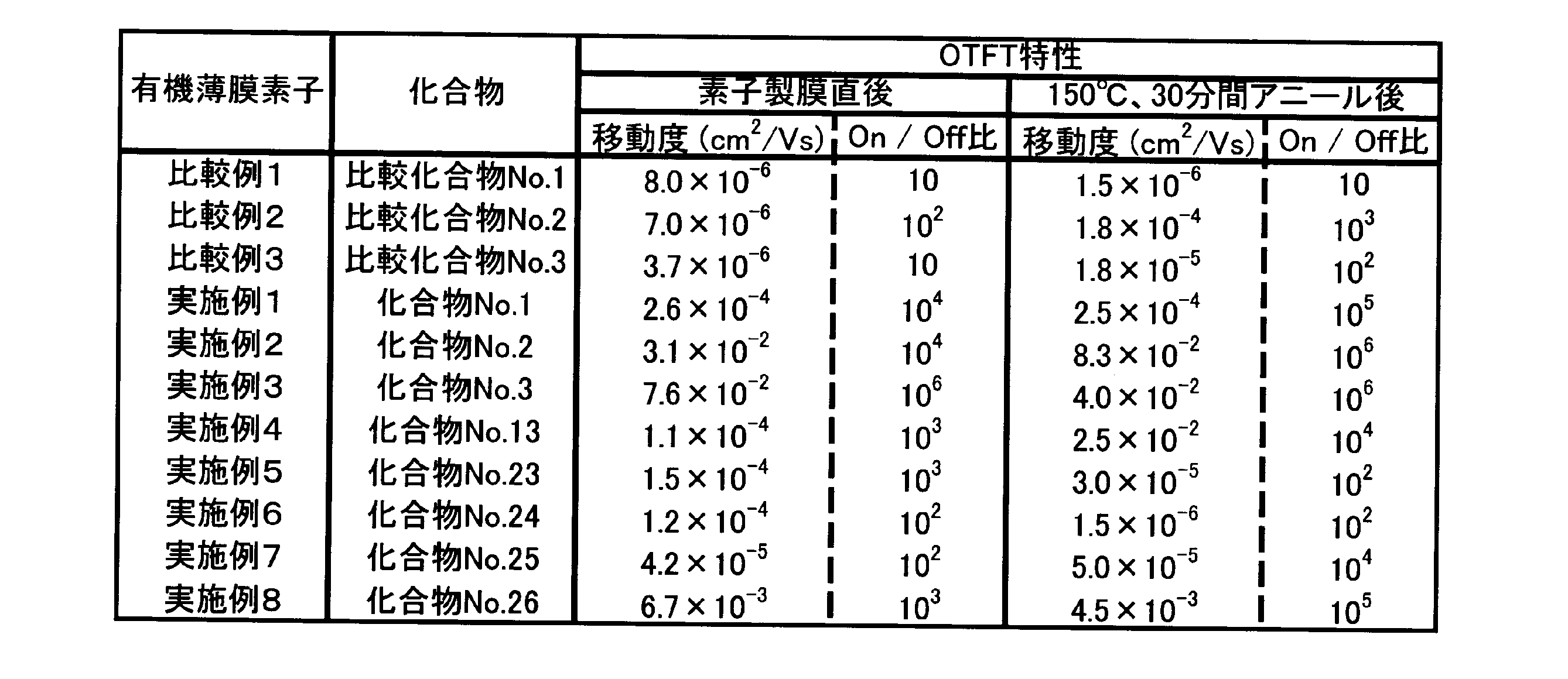
〔表1〕の結果より、特定の構造を有するペリレンテトラカルボン酸ジイミド化合物を含有する本発明の有機半導体材料を用いて作製したOTFT素子は、比較化合物を含有する有機半導体材料を用いて作製したOTFT素子に比べ、電荷移動度及びOn/Off比に優れることが明らかである。また、アニール後においても、比較化合物を含有する有機半導体材料に対する本発明の有機半導体材料の優位性は変わらなかった。
〔実施例9〕
図2に示す層構成を有する有機薄膜トランジスタ(OTFT)素子を、以下の手順で作製した。
Si処理基板上に、有機半導体材料として化合物No.3を高真空下(10-4~10-3Pa)にて、蒸着速度0.02nm/secで30nm積層し、有機半導体層11とした。この有機半導体層11の表面にパターニングされたニッケルマスクを重ね、金を用いて真空蒸着することにより、ソース電極13及びドレイン電極12を形成して、OTFT素子とした。このソース電極13及びドレイン電極12は、チャネル幅5mm、チャネル長20μmにて形成した。
図2に示す層構成を有する有機薄膜トランジスタ(OTFT)素子を、以下の手順で作製した。
Si処理基板上に、有機半導体材料として化合物No.3を高真空下(10-4~10-3Pa)にて、蒸着速度0.02nm/secで30nm積層し、有機半導体層11とした。この有機半導体層11の表面にパターニングされたニッケルマスクを重ね、金を用いて真空蒸着することにより、ソース電極13及びドレイン電極12を形成して、OTFT素子とした。このソース電極13及びドレイン電極12は、チャネル幅5mm、チャネル長20μmにて形成した。
作製したOTFT素子は、正のゲート電圧を印加するに従い、ドレイン電流が増強するnチャネル-エンハンス型の動作特性を示した。作製したOTFT素子において、I-V特性の飽和領域から電荷移動度を求め、更にOn/Off比(Vd=80Vとし、Vgを80~0Vにしたときのドレイン電流値の比)を算出したところ、電荷移動度5.3×10-2cm2/Vs、On/Off比105の値を示した。また、このOTFT素子を70℃、30分間の条件で加熱した後、同様に評価したところ、電荷移動度1.0×10-1cm2/Vs、On/Off比107の値を示した。
実施例1~9の結果から明らかなように、本発明のペリレンカルボン酸ジイミド化合物を少なくとも一種含有してなる有機半導体材料はウェットプロセスによる製膜に適するのみならず、真空蒸着等のドライプロセスによっても製膜が可能であり、何れのプロセスで製膜した有機半導体素子も高いキャリア移動度を示すことは明白である。
11 有機半導体層
12 ドレイン電極
13 ソース電極
14 絶縁層
15 ゲート電極
16 基板
12 ドレイン電極
13 ソース電極
14 絶縁層
15 ゲート電極
16 基板
Claims (6)
- 下記一般式(I)で表されるペリレンカルボン酸ジイミド化合物を少なくとも一種含有してなる有機半導体材料。

- R1及びR1'が炭素原子数10~30の無置換アルキル基又は炭素原子数10~30の置換アルキル基を表す請求項1に記載の有機半導体材料。
- 上記無置換アルキル基及び上記置換アルキル基が分岐構造を有する請求項1又は2に記載の有機半導体材料。
- R1及びR1'が上記無置換アルキル基である請求項1~3の何れか一項に記載の有機半導体材料。
- 請求項1~4の何れか一項に記載の有機半導体材料を製膜してなる有機半導体層。
- 請求項5に記載の有機半導体層を少なくとも1層有する有機半導体素子。
Priority Applications (1)
| Application Number | Priority Date | Filing Date | Title |
|---|---|---|---|
| JP2012501710A JP5793134B2 (ja) | 2010-02-25 | 2011-01-25 | ペリレンテトラカルボン酸ジイミド化合物を含有してなる有機半導体材料、及び有機半導体素子 |
Applications Claiming Priority (2)
| Application Number | Priority Date | Filing Date | Title |
|---|---|---|---|
| JP2010040601 | 2010-02-25 | ||
| JP2010-040601 | 2010-02-25 |
Publications (1)
| Publication Number | Publication Date |
|---|---|
| WO2011105152A1 true WO2011105152A1 (ja) | 2011-09-01 |
Family
ID=44506574
Family Applications (1)
| Application Number | Title | Priority Date | Filing Date |
|---|---|---|---|
| PCT/JP2011/051324 Ceased WO2011105152A1 (ja) | 2010-02-25 | 2011-01-25 | ペリレンテトラカルボン酸ジイミド化合物を含有してなる有機半導体材料、及び有機半導体素子 |
Country Status (3)
| Country | Link |
|---|---|
| JP (1) | JP5793134B2 (ja) |
| TW (1) | TWI500615B (ja) |
| WO (1) | WO2011105152A1 (ja) |
Cited By (5)
| Publication number | Priority date | Publication date | Assignee | Title |
|---|---|---|---|---|
| CN102584822A (zh) * | 2011-12-14 | 2012-07-18 | 上海交通大学 | 稠合三氟甲基的苯并咪唑萘酰亚胺衍生物、制备方法及用途 |
| JP2014015461A (ja) * | 2012-07-05 | 2014-01-30 | Peking Univ | 分岐アルキル鎖を有する化合物、その製造方法及び光電デバイス中における使用 |
| WO2020100783A1 (ja) * | 2018-11-13 | 2020-05-22 | 住友化学株式会社 | 着色組成物 |
| JP2021125476A (ja) * | 2020-01-31 | 2021-08-30 | 保土谷化学工業株式会社 | ペリレン誘導体化合物、該化合物を用いた有機半導体用組成物、該有機半導体用組成物を用いた有機薄膜トランジスタ |
| WO2025179782A1 (zh) * | 2024-02-28 | 2025-09-04 | 江苏集萃智能液晶科技有限公司 | 一种有机化合物及其应用 |
Family Cites Families (2)
| Publication number | Priority date | Publication date | Assignee | Title |
|---|---|---|---|---|
| DE2636421A1 (de) * | 1976-08-13 | 1978-02-16 | Basf Ag | Elektrisch leitfaehige perylenderivate |
| JP5148211B2 (ja) * | 2007-08-30 | 2013-02-20 | 出光興産株式会社 | 有機薄膜トランジスタ及び有機薄膜発光トランジスタ |
-
2011
- 2011-01-25 WO PCT/JP2011/051324 patent/WO2011105152A1/ja not_active Ceased
- 2011-01-25 JP JP2012501710A patent/JP5793134B2/ja not_active Expired - Fee Related
- 2011-02-09 TW TW100104327A patent/TWI500615B/zh not_active IP Right Cessation
Non-Patent Citations (1)
| Title |
|---|
| FABIAN NOLDE ET AL.: "Synthesis and Self- Organization of Core-Extended Perylene Tetracarboxdiimides with Branched Alkyl Substituents", CHEMISTRY OF MATERIALS, vol. 18, no. ISS.16, 15 July 2006 (2006-07-15), pages 3715 - 3725 * |
Cited By (9)
| Publication number | Priority date | Publication date | Assignee | Title |
|---|---|---|---|---|
| CN102584822A (zh) * | 2011-12-14 | 2012-07-18 | 上海交通大学 | 稠合三氟甲基的苯并咪唑萘酰亚胺衍生物、制备方法及用途 |
| CN102584822B (zh) * | 2011-12-14 | 2014-08-06 | 上海交通大学 | 稠合三氟甲基的苯并咪唑萘酰亚胺衍生物、制备方法及用途 |
| JP2014015461A (ja) * | 2012-07-05 | 2014-01-30 | Peking Univ | 分岐アルキル鎖を有する化合物、その製造方法及び光電デバイス中における使用 |
| WO2020100783A1 (ja) * | 2018-11-13 | 2020-05-22 | 住友化学株式会社 | 着色組成物 |
| KR20210088554A (ko) | 2018-11-13 | 2021-07-14 | 스미또모 가가꾸 가부시키가이샤 | 착색 조성물 |
| KR102823995B1 (ko) | 2018-11-13 | 2025-06-23 | 스미또모 가가꾸 가부시키가이샤 | 착색 조성물 |
| JP2021125476A (ja) * | 2020-01-31 | 2021-08-30 | 保土谷化学工業株式会社 | ペリレン誘導体化合物、該化合物を用いた有機半導体用組成物、該有機半導体用組成物を用いた有機薄膜トランジスタ |
| JP7464397B2 (ja) | 2020-01-31 | 2024-04-09 | 保土谷化学工業株式会社 | ペリレン誘導体化合物、該化合物を用いた有機半導体用組成物、該有機半導体用組成物を用いた有機薄膜トランジスタ |
| WO2025179782A1 (zh) * | 2024-02-28 | 2025-09-04 | 江苏集萃智能液晶科技有限公司 | 一种有机化合物及其应用 |
Also Published As
| Publication number | Publication date |
|---|---|
| TWI500615B (zh) | 2015-09-21 |
| JPWO2011105152A1 (ja) | 2013-06-20 |
| JP5793134B2 (ja) | 2015-10-14 |
| TW201144308A (en) | 2011-12-16 |
Similar Documents
| Publication | Publication Date | Title |
|---|---|---|
| JP5665137B2 (ja) | 有機半導体材料、有機半導体薄膜および有機薄膜トランジスタ | |
| Chen et al. | Asymmetric fused thiophenes for field-effect transistors: crystal structure–film microstructure–transistor performance correlations | |
| JP6080870B2 (ja) | 溶液プロセス用有機半導体材料及び有機半導体デバイス | |
| Kim et al. | Functionalized dithieno [2, 3-b: 3′, 2′-d] thiophenes (DTTs) for organic thin-film transistors | |
| JP5793134B2 (ja) | ペリレンテトラカルボン酸ジイミド化合物を含有してなる有機半導体材料、及び有機半導体素子 | |
| WO2017028460A1 (zh) | 一类九元稠环衍生物及其合成方法与应用 | |
| US7932463B2 (en) | Quinacridine derivatives and organic electronic devices using the same | |
| KR20130133903A (ko) | 페릴렌테트라카르복실산 비스이미드 유도체, n-형 반도체, n-형 반도체의 제조 방법, 및 전자 장치 | |
| JP5897050B2 (ja) | 有機薄膜トランジスタ、有機半導体薄膜および有機半導体材料 | |
| Yamada et al. | Synthesis of perfluoroalkylated pentacenes and evaluation of their fundamental physical properties | |
| CN102574806B (zh) | 苝四甲酰二亚胺衍生物 | |
| KR20150142043A (ko) | 파이-연장된 나프탈렌 디이미드의 제조 및 반도체로서의 그의 용도 | |
| Chien et al. | Tetracene-based field-effect transistors using solution processes | |
| JP5670216B2 (ja) | 新規ビベンゾ[b]フラン化合物、並びに該化合物を含有してなる有機半導体材料及び有機半導体素子 | |
| JPWO2012029544A1 (ja) | 有機半導体微粒子材料、有機半導体薄膜、有機半導体膜形成用分散液、有機半導体薄膜の製造方法および有機薄膜トランジスタ | |
| JP6474276B2 (ja) | ピセノジチオフェン化合物、有機半導体材料、有機半導体層、有機半導体素子 | |
| JP5228411B2 (ja) | [1]ベンゾカルコゲノ[3,2−b][1]ベンゾカルコゲノフェン骨格を有する化合物およびこれを用いた有機トランジスタ | |
| US20110177653A1 (en) | Thiazole-based semiconductor compound and organic thin film transistor using the same | |
| TWI477489B (zh) | An n-type semiconductor composed of a fullerene compound | |
| JP2010083785A (ja) | 平面性の高い分子構造を有する化合物およびこれを用いた有機トランジスタ | |
| JP2015140332A (ja) | 金属錯体、金属錯体溶液、薄膜及びその製造方法、電子素子、薄膜トランジスタ、表示装置、イメージセンサ、並びにx線センサ | |
| JP5458267B2 (ja) | ヘキサメチレンテトラチアフルバレン化合物、有機半導体および有機薄膜トランジスタ | |
| JP6093493B2 (ja) | クリセン化合物を使用した有機半導体デバイス。 | |
| WO2019176634A1 (ja) | n型有機半導体材料、有機半導体膜形成用組成物、有機半導体膜及びその製造方法、有機薄膜トランジスタ及びその製造方法、並びに化合物の製造方法 | |
| CN102977084A (zh) | 噻吩吡咯醌型结构n-型半导体材料的合成及包含该材料的半导体设备 |
Legal Events
| Date | Code | Title | Description |
|---|---|---|---|
| 121 | Ep: the epo has been informed by wipo that ep was designated in this application |
Ref document number: 11747116 Country of ref document: EP Kind code of ref document: A1 |
|
| WWE | Wipo information: entry into national phase |
Ref document number: 2012501710 Country of ref document: JP |
|
| NENP | Non-entry into the national phase |
Ref country code: DE |
|
| 122 | Ep: pct application non-entry in european phase |
Ref document number: 11747116 Country of ref document: EP Kind code of ref document: A1 |