WO2011104943A1 - 液晶表示パネル及び液晶表示装置 - Google Patents
液晶表示パネル及び液晶表示装置 Download PDFInfo
- Publication number
- WO2011104943A1 WO2011104943A1 PCT/JP2010/069746 JP2010069746W WO2011104943A1 WO 2011104943 A1 WO2011104943 A1 WO 2011104943A1 JP 2010069746 W JP2010069746 W JP 2010069746W WO 2011104943 A1 WO2011104943 A1 WO 2011104943A1
- Authority
- WO
- WIPO (PCT)
- Prior art keywords
- liquid crystal
- crystal display
- display panel
- wiring
- reflectance
- Prior art date
- Legal status (The legal status is an assumption and is not a legal conclusion. Google has not performed a legal analysis and makes no representation as to the accuracy of the status listed.)
- Ceased
Links
Images







Classifications
-
- G—PHYSICS
- G02—OPTICS
- G02F—OPTICAL DEVICES OR ARRANGEMENTS FOR THE CONTROL OF LIGHT BY MODIFICATION OF THE OPTICAL PROPERTIES OF THE MEDIA OF THE ELEMENTS INVOLVED THEREIN; NON-LINEAR OPTICS; FREQUENCY-CHANGING OF LIGHT; OPTICAL LOGIC ELEMENTS; OPTICAL ANALOGUE/DIGITAL CONVERTERS
- G02F1/00—Devices or arrangements for the control of the intensity, colour, phase, polarisation or direction of light arriving from an independent light source, e.g. switching, gating or modulating; Non-linear optics
- G02F1/01—Devices or arrangements for the control of the intensity, colour, phase, polarisation or direction of light arriving from an independent light source, e.g. switching, gating or modulating; Non-linear optics for the control of the intensity, phase, polarisation or colour
- G02F1/13—Devices or arrangements for the control of the intensity, colour, phase, polarisation or direction of light arriving from an independent light source, e.g. switching, gating or modulating; Non-linear optics for the control of the intensity, phase, polarisation or colour based on liquid crystals, e.g. single liquid crystal display cells
- G02F1/133—Constructional arrangements; Operation of liquid crystal cells; Circuit arrangements
- G02F1/1333—Constructional arrangements; Manufacturing methods
- G02F1/1335—Structural association of cells with optical devices, e.g. polarisers or reflectors
- G02F1/133509—Filters, e.g. light shielding masks
- G02F1/133514—Colour filters
-
- G—PHYSICS
- G02—OPTICS
- G02F—OPTICAL DEVICES OR ARRANGEMENTS FOR THE CONTROL OF LIGHT BY MODIFICATION OF THE OPTICAL PROPERTIES OF THE MEDIA OF THE ELEMENTS INVOLVED THEREIN; NON-LINEAR OPTICS; FREQUENCY-CHANGING OF LIGHT; OPTICAL LOGIC ELEMENTS; OPTICAL ANALOGUE/DIGITAL CONVERTERS
- G02F1/00—Devices or arrangements for the control of the intensity, colour, phase, polarisation or direction of light arriving from an independent light source, e.g. switching, gating or modulating; Non-linear optics
- G02F1/01—Devices or arrangements for the control of the intensity, colour, phase, polarisation or direction of light arriving from an independent light source, e.g. switching, gating or modulating; Non-linear optics for the control of the intensity, phase, polarisation or colour
- G02F1/13—Devices or arrangements for the control of the intensity, colour, phase, polarisation or direction of light arriving from an independent light source, e.g. switching, gating or modulating; Non-linear optics for the control of the intensity, phase, polarisation or colour based on liquid crystals, e.g. single liquid crystal display cells
- G02F1/133—Constructional arrangements; Operation of liquid crystal cells; Circuit arrangements
- G02F1/1333—Constructional arrangements; Manufacturing methods
- G02F1/1335—Structural association of cells with optical devices, e.g. polarisers or reflectors
- G02F1/133553—Reflecting elements
-
- G—PHYSICS
- G02—OPTICS
- G02F—OPTICAL DEVICES OR ARRANGEMENTS FOR THE CONTROL OF LIGHT BY MODIFICATION OF THE OPTICAL PROPERTIES OF THE MEDIA OF THE ELEMENTS INVOLVED THEREIN; NON-LINEAR OPTICS; FREQUENCY-CHANGING OF LIGHT; OPTICAL LOGIC ELEMENTS; OPTICAL ANALOGUE/DIGITAL CONVERTERS
- G02F1/00—Devices or arrangements for the control of the intensity, colour, phase, polarisation or direction of light arriving from an independent light source, e.g. switching, gating or modulating; Non-linear optics
- G02F1/01—Devices or arrangements for the control of the intensity, colour, phase, polarisation or direction of light arriving from an independent light source, e.g. switching, gating or modulating; Non-linear optics for the control of the intensity, phase, polarisation or colour
- G02F1/13—Devices or arrangements for the control of the intensity, colour, phase, polarisation or direction of light arriving from an independent light source, e.g. switching, gating or modulating; Non-linear optics for the control of the intensity, phase, polarisation or colour based on liquid crystals, e.g. single liquid crystal display cells
- G02F1/133—Constructional arrangements; Operation of liquid crystal cells; Circuit arrangements
- G02F1/136—Liquid crystal cells structurally associated with a semi-conducting layer or substrate, e.g. cells forming part of an integrated circuit
- G02F1/1362—Active matrix addressed cells
- G02F1/136286—Wiring, e.g. gate line, drain line
Definitions
- the present invention relates to a liquid crystal display panel and a liquid crystal display device. More specifically, the present invention relates to a liquid crystal display panel and a liquid crystal display device suitable for increasing the number of colors and increasing the definition.
- the liquid crystal display device has been attracting attention as a display device that can achieve light weight, thinness, and low power consumption, and is indispensable for daily life and business, such as mobile applications, various monitors, and large televisions.
- an active matrix liquid crystal display device using a thin film transistor (TFT) as a pixel switching element (driving element) has a large market scale due to a high contrast ratio and a high response speed.
- TFT thin film transistor
- driving element driving element
- a conventional liquid crystal display device has a structure in which liquid crystal is sealed between two transparent substrates, and one of the two opposing surfaces of the transparent substrate has a counter electrode and a color on one surface side.
- a filter, an alignment film, and the like are formed, a TFT, a pixel electrode (display electrode and common electrode), an alignment film, and the like are formed on the other surface side.
- a plurality of gate bus lines and a plurality of data intersecting with the gate bus lines A device including a liquid crystal display panel in which a bus line is formed is disclosed (for example, see Patent Document 1).
- a black matrix is formed in parallel with the data bus line as an embodiment, and the width of the data bus line is 4 ⁇ m, whereas the width of the black matrix is set to 8 ⁇ m.
- a substrate using copper or a copper alloy as a conductive film or a conductive line is disclosed (for example, see Patent Documents 2 to 4).
- JP 2000-267141 A (FIG. 7 on pages 1, 2, 11, 18) JP 2008-66680 A (2nd and 6th pages) JP 2008-66678 A (pages 2 and 6) JP 2008-28395 A (pages 2 and 7)
- the liquid crystal display panel (LCD panel) manufactured so far has a TFT element when the panel main surface is viewed in plan view, for example, as shown in FIG.
- the black matrix is disposed only at positions such as between the picture elements, on the spacers, and the area to be shielded from light is suppressed.
- the TFT light shielding is performed in each of the picture element in which the red color filter 322R is arranged, the picture element in which the green color filter 322G is arranged, and the picture element in which the blue color filter 322B is arranged.
- a black matrix 321T as a part and a black matrix 321S as a spacer light-shielding part are arranged. Further, a black matrix 321P as an inter-picture element light-shielding portion is arranged. On the other hand, the black matrix is not arranged on the other auxiliary capacitance wiring 311a and the gate wiring 311b. Therefore, the exposure ratio of the metal wiring on the TFT substrate in the picture element is large.
- metal wiring metal wiring
- the resistance value is more than that used so far.
- metal wiring that can improve performance has high reflectivity, so when external light is incident on the panel, many reflections occur in the panel due to the reflection of the metal wiring, and the display quality is reduced. There was a problem of a decrease. That is, in the case of a conventional LCD panel, particularly when it is constituted by a plurality of types of metal wirings such as a TFT substrate, the reflection of light from the metal wirings on the substrate causes coloration due to reflection of external light and a decrease in bright room contrast. It was.
- the present invention has been made in view of the above-described present situation, and is provided with metal wiring, and in particular, in a form constituted by a plurality of types of metal wiring such as a TFT substrate, coloring is reduced and bright room contrast is improved. It is an object of the present invention to provide a liquid crystal display panel and a liquid crystal display device including such a liquid crystal display panel.
- the inventors of the present invention have made various studies on a liquid crystal display panel and a liquid crystal display device provided with a metal wiring, and the metal wiring has a high spectral reflectance in a specific wavelength region in the wavelength region of visible light. It was discovered that a large amount of reflected light on the substrate was generated in the liquid crystal display panel with the incidence of light, causing coloration due to external light reflection and a decrease in bright room contrast. In particular, when a plurality of types of metal wirings are used as in the case of a TFT substrate, or when the metal wiring is a low-resistance wiring, such a problem occurs remarkably.
- the present invention is a liquid crystal display panel having a wiring composed of a metal having a wavelength region with a reflectance of 90% or more in the visible light region, and the liquid crystal display panel is on the display surface side at a wavelength of 550 nm.
- the liquid crystal display panel has a reflectance of 150% or less on the display surface side at a wavelength of 600 to 700 nm with respect to the reflectance.
- the reflectance is 550 nm, which is the central wavelength of white balance obtained by combining the colors.
- the black matrix is additionally arranged so that the reflectance within the range of 600 to 700 nm is 150% or less.
- the reflectance within the range of 600 to 700 nm is 150% or less.
- the reflectance is 150% or less.
- the reddish brown coloring in the liquid crystal display panel can be sufficiently reduced, and the bright room contrast can be improved.
- the reflectivity is measured using an integrating sphere (a sphere coated with a white paint such as barium sulfate that diffuses and reflects light almost completely). Can be measured by a method of receiving light from one direction.
- the said reflectance means the reflectance of the light reflected toward the display surface side (viewer side) of a display panel.
- the upper limit of the reflectance may be such that the minimum reflectance within the range of 600 to 700 nm in the display panel is 150% or less, but the average reflectance is more preferably 150% or less. Most preferably, the maximum reflectance in the range of 600 to 700 nm in the display panel is 150% or less.
- the lower limit value of the reflectivity may be such that the highest reflectivity within the range of 600 to 700 nm satisfies the lower limit value, that is, it is not less than the lower limit value, but the average reflectivity satisfies the lower limit value. More preferred. Most preferably, the minimum reflectance within the range of 600 to 700 nm in the display panel satisfies the lower limit.
- the metal in the liquid crystal display panel of the present invention examples include silver, gold, copper, and alloys thereof. Among them, those having a reflectance of 90% or more at a wavelength of 600 to 700 nm are preferable. More preferably, the reflectance is 95% or more. Especially, it is preferable that the said metal is copper or its alloy.
- the black matrix formed on the color filter substrate is partially additionally arranged so that the color by the metal wiring is more preferable. Can be reduced. That is, the embodiment in which the reflectance is 90% or more is suitably applied when the surface layer portion of the metal wiring is made of the above metal, and it is evaluated that reflection of incident light is usually generated. However, by adopting the configuration of the present invention, it is possible to sufficiently obtain the effect of sufficiently suppressing problems caused by reflected light.
- the configuration of the liquid crystal display panel and the liquid crystal display device of the present invention is not particularly limited by other components as long as such components are essential. Preferred embodiments of the liquid crystal display panel and the liquid crystal display device of the present invention will be described in detail below.
- the wiring when the main surface of the panel is viewed in plan, the wiring has 75% or more of the surface area of the metal superimposed on the light shielding layer in the pixel displaying red.
- the form which is is mentioned. By such a form, reddish brown coloring can be reduced suitably.
- the upper limit value of the overlapping ratio with the metal light-shielding layer is, for example, 100%. Note that the reflectance measurement conditions are the same as described above.
- the preferred form is particularly effective when a low-resistance wiring having a unique color of red, such as copper or an alloy thereof, is used.
- the overlapping ratio with the metal light-shielding layer is increased by 30% or more in the pixel displaying red color with respect to the conventional metal exposed area. It is preferable to additionally arrange a black matrix. That is, a black matrix is arranged only on the TFT element, on the spacer, and between the picture elements, and in the picture element displaying red, the metal is 30% or more of the area where the metal is exposed in other places. It is preferable to increase the overlapping ratio with the light shielding layer. More preferably, the overlapping ratio with the metal light-shielding layer is increased by 30% or more only in the picture element displaying red. In these cases, the additional ratio of the black matrix area is 30% or more.
- the metal exposed area is an area of a region in the liquid crystal display panel where reflection by metal occurs when external light is incident. Normally, the metal wiring is covered with various films and the like, but reflection occurs in a region that does not overlap with a light shielding layer such as a black matrix when viewed in plan. In the present specification, the term “exposure” is used to mean that the structure is not covered with a light shielding layer such as a black matrix when viewed in plan.
- a black matrix is arranged on the TFT element, the spacer, and between the picture elements in the picture element displaying red, and black is also formed on a part of the gate bus line and / or the auxiliary capacity wiring. It is preferable to arrange the matrix.
- the black matrix is arranged in 30% or more of the metal exposed area (area of the metal reflection region) of the gate bus line and the auxiliary capacitance wiring, preferably in the above% range.
- the metal exposed area of the gate bus line and the auxiliary capacitance wiring is a metal exposed area in a portion excluding the area already shielded by the black matrix arranged on the TFT element, the spacer, and between the picture elements.
- the overlapping ratio of the picture element displaying red with the metal light-shielding layer and the metal exposed area have been described.
- RGBY4 primary color with yellow (Y) picture element added or RGBC4 primary color with cyan (C) picture element added, or more primary liquid crystal display panel with RGBY or RGBC as essential It is preferable that the present invention is applied to a yellow picture element and / or a cyan picture element together with the picture element to be processed.
- a black matrix is additionally arranged for red, yellow and / or cyan picture elements, and a black matrix is not additionally arranged for the other picture elements in the same manner as in the above form.
- the yellow and cyan picture elements are colored reddish brown as the metal is exposed, similar to the red picture elements. More preferably, in a liquid crystal display panel in which RGBY is essential, it is applied to a yellow picture element as well as a picture element displaying red.
- the black matrix is arranged only on the TFT element, the spacer, and between the picture elements, and the red, yellow, and / or cyan picture elements with respect to the area of the region where the metal is exposed in other places.
- the upper limit value of the overlapping ratio with the metal light-shielding layer is, for example, 100%.
- the additional ratio of the black matrix additionally arranged in the red pixels is yellow and / or It is preferable to make the ratio larger than the additional ratio of the black matrix area additionally arranged in the cyan picture element.
- the additional ratio of the black matrix area in the red picture element is 50% or more, and the additional ratio of the black matrix area in the yellow and / or cyan picture element is 30% or more and less than 50%.
- the effect of the light reflection on the metal wiring on the contrast of the red picture element is greater than that of the yellow or cyan picture element, especially when using a metal wiring whose surface layer is copper or an alloy containing copper. Since the picture element is usually the largest, it is affected by the contrast of the reddish brown color.
- a display device in which a display surface is configured by pixels having red, green, blue, and yellow sub-pixels, the red and / or blue sub-pixels being other A mode in which the aperture area is larger than the sub-pixel (a mode in which the aperture area of the red sub-pixel is the maximum, a mode in which the aperture area of the blue sub-pixel is the maximum, and a sub-pixel in red and blue
- the green and / or yellow sub-pixel has a smaller opening area than the other sub-pixels (the green sub-pixel has the smallest opening area than the other sub-pixels).
- the opening area of the yellow sub-pixel is minimum, and a form in which the opening areas of both the green and yellow sub-pixels are minimum).
- yellow can be replaced with cyan.
- the pixel may include a red and / or blue sub-pixel having different color characteristics. In these four primary colors or four or more primary color liquid crystal display devices, visibility is impaired by increasing the number of primary colors used for display, in particular, by reducing the lightness of red. Further, when a light source having a high color temperature is used to adjust the color tone of white display, the brightness of red display is further lowered, and accordingly, visibility is further impaired.
- the wiring is light-shielding having at least a part of the same width and / or narrower width than the wiring when the panel main surface is viewed in plan.
- the form which has overlapped with the layer is mentioned. More preferably, the light-emitting layer is overlapped with a light-shielding layer having a narrower width than the wiring.
- the width of the black matrix will be arranged slightly larger than the width of the metal wiring in consideration of errors during production, etc. A reduction in contrast due to light reflection of the metal wiring can be suppressed, and an effect of improving the transmittance by improving the aperture ratio can be sufficiently obtained.
- the color while preferably adjusting the light shielding ratio.
- the metal wiring overlaps with the light shielding layer having substantially the same width and / or narrower width than the wiring in the preferred embodiment in which the black matrix is additionally disposed. It is preferable to apply to the black matrix to be arranged.
- a black matrix is arranged on the TFT element, the spacer, and between the pixels, and a black matrix is also arranged on a part of the gate bus line and / or the auxiliary capacitance line, and the gate bus line and / or the auxiliary capacitance line is arranged. It is preferable that at least a portion overlaps with a black matrix having substantially the same width and / or narrower width than the wiring.
- the light-emitting layer overlaps with a light-shielding layer having a narrower width than the wiring.
- the above-mentioned wiring is in a form in which the surface layer portion is copper or an alloy containing copper, reddish brown coloring is suitably reduced while taking advantage of low resistance by using such metal wiring.
- the above-described embodiment and the preferable embodiment of the present invention are applied to a liquid crystal display panel including an active matrix substrate using a thin film transistor (TFT).
- TFT thin film transistor
- the present invention is also a liquid crystal display device including the liquid crystal display panel of the present invention. As a result, it is possible to obtain a liquid crystal display device with reduced coloring and excellent bright room contrast.
- coloring can be reduced and bright room contrast can be improved.
- FIG. 3 is a schematic plan view illustrating pixels of the liquid crystal display panel of Embodiment 1.
- FIG. 4 is a partially enlarged view showing source wiring of the liquid crystal display panel of Embodiment 1.
- FIG. It is a graph which shows the spectral reflectance of a copper wiring, an aluminum wiring, and a titanium wiring.
- 3 is a graph showing the spectral reflectance of the liquid crystal display panel of Embodiment 1.
- It is a graph which shows the spectral reflectance of the liquid crystal display panel of Embodiment 1, and the spectral reflectance of the liquid crystal display panel of the comparative example 1 when the reflectance in wavelength 550nm is 100%.
- FIG. 5 is a graph showing reflected light chromaticity of the liquid crystal display panel of Embodiment 1 and reflected light chromaticity of the liquid crystal display panel of Comparative Example 1.
- FIG. 6 is a schematic plan view illustrating pixels of a liquid crystal display panel according to a modified example of Embodiment 1.
- FIG. 6 is a schematic plan view illustrating pixels of a liquid crystal display panel of Embodiment 2.
- FIG. 6 is a graph showing the spectral reflectance of the liquid crystal display panel of Embodiment 2. It is a graph which shows the spectral reflectance of the liquid crystal display panel of Embodiment 2, and the spectral reflectance of the liquid crystal display panel of the comparative example 2 when the reflectance in 550 nm is 100%.
- FIG. 6 is a graph showing the reflected light chromaticity of the liquid crystal display panel of Embodiment 2 and the reflected light chromaticity of the liquid crystal display panel of Comparative Example 2. It is a plane schematic diagram which shows the circuit board in this embodiment. It is a disassembled perspective schematic diagram which shows the structure of the liquid crystal panel in this embodiment.
- FIG. 14 is an exploded perspective schematic diagram illustrating a structure of a liquid crystal display device including the liquid crystal panel illustrated in FIG. 13.
- 6 is a schematic cross-sectional view showing external light reflection of the liquid crystal display panel of Comparative Example 1.
- FIG. 6 is a schematic plan view showing pixels of a liquid crystal display panel of Comparative Example 1.
- FIG. 10 is a graph showing the spectral reflectance of the liquid crystal display panel of Comparative Example 1.
- 10 is a schematic plan view showing pixels of a liquid crystal display panel of Comparative Example 2.
- FIG. 10 is a graph showing the spectral reflectance of the liquid crystal display panel of Comparative Example 2.
- the circuit substrate is also referred to as a TFT side substrate because it is a substrate on which TFTs are provided in the embodiment.
- the substrate facing the circuit substrate is also a substrate on which a color filter (CF) is arranged in the embodiment, and is also referred to as a CF side substrate.
- the surface layer portion refers to a layer portion on the display surface side of the display panel.
- the reflectance is measured using an integrating sphere (a sphere coated with a white paint such as barium sulfate that diffuses and reflects light almost completely). Was performed by a method of receiving light from one direction.
- the liquid crystal display panel of Embodiment 1 is obtained by the following (1) to (4).
- the procedure is not particularly limited to this procedure.
- the TFT substrate was a substrate in which copper wiring, which is low resistance wiring, was used as metal wiring.
- a copper alloy can also be suitably used.
- all of the surface layers of the gate wiring, the auxiliary capacitance wiring, and the source wiring are high reflectance wiring (copper wiring), but a metal with high reflectance is part of the wiring surface layer portion.
- only the surface layer of the gate wiring may be a high reflectance wiring.
- the surface state of the metal wiring may be flat or uneven as long as the reflectance is specified.
- the form in which the surface layer is a high reflectance wiring includes a form in which the high reflectance wiring is exposed on the surface layer, such as a form in which a transparent electrode is formed on the high reflectance wiring.
- the color filter substrate used was composed of three colors of R (red), G (green), and B (blue).
- the black matrix of the color filter substrate in addition to the conventional TFT elements, the spacers, and between the picture elements, the black matrix is additionally arranged only for the R picture elements. A 30% black matrix was added to only the R picture element with respect to the conventional exposed metal area.
- the substrate of (1) and the color filter substrate of (2) were bonded together, and liquid crystal was sealed to form a liquid crystal display device.
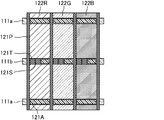
- FIG. 1 is a schematic plan view showing pixels of the liquid crystal display panel of Embodiment 1.
- the liquid crystal display panel of Embodiment 1 has a black matrix arranged on the TFT elements, on the spacers, and between the picture elements when the panel main surface is viewed in plan.
- a black matrix 21T as a TFT light shielding unit
- a black matrix 21S is disposed as a spacer light-shielding portion.
- a black matrix 21P as an inter-picture element light-shielding portion is arranged.
- an additional black matrix 21A is arranged on the auxiliary capacitance line 11a and the gate line 11b.
- 75% or more of the surface area of the metal overlaps with the light-shielding layer in the picture element displaying red when the main surface of the panel is viewed in plan.
- the ratio of the additional arrangement is 30% with respect to the conventional exposed metal area in the red picture element.
- the additional black matrix 21A has a width narrower than that of the storage capacitor line 11a and the width of the gate line 11b.
- the color arrangement of the color filter in the first embodiment is an RGB repeating arrangement, and the area ratio is 1.0: 1.0: 1.0.
- FIG. 2 is a partially enlarged view showing the source wiring of the liquid crystal display panel of the first embodiment.
- the source wiring 13S is arranged in a zigzag shape and the panel main surface is viewed in plan, a part of the source wiring 13S is in the red picture element and the other part is in the picture element other than the red picture element (for example, In blue picture element).
- the black matrix is arranged so as to overlap at least the source wiring 13S in the red picture element. More preferably, from the viewpoint of transmittance, the black matrix is arranged so as to overlap with the source line 13S only in the red picture element.
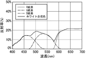
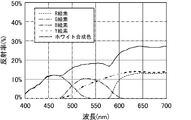
- FIG. 3 is a graph showing the spectral reflectance of copper wiring, aluminum wiring, and titanium wiring.
- FIG. 3 shows the spectral reflectance of the copper wiring used in the liquid crystal display panel of this embodiment.
- the copper wiring has a reflectance of 90% or more in the wavelength range of 590 to 700 nm.
- the aluminum wiring and the titanium wiring have a reflectance of less than 90% in the visible light region, and although they are not as low in resistance as the copper wiring, the degree of coloring is originally small.
- FIG. 4 is a graph showing the spectral reflectance of the liquid crystal display panel of the first embodiment.
- R picture element red picture element
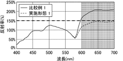
- FIG. 5 is a graph showing the spectral reflectance of the liquid crystal display panel of Embodiment 1 and the spectral reflectance of the liquid crystal display panel of Comparative Example 1 when the reflectance at a wavelength of 550 nm is 100%.
- the reflectance on the display surface side at a wavelength of 600 to 700 nm is 150% or less with respect to the reflectance on the display surface side at a wavelength of 550 nm.
- FIG. 6 is a graph showing the reflected light chromaticity of the liquid crystal display panel of Embodiment 1 and the reflected light chromaticity of the liquid crystal display panel of Comparative Example 1.
- FIG. 6 shows the XYZ color system. “Black body” in FIG. 6 indicates a black body locus on the xy chromaticity diagram. In the graph of FIG. 6, the right side is reddish, the left side is blued, and the upper side is greenish. The same applies to FIG.
- a black matrix is arranged in a part of the exposed portion of the metal wiring on the TFT substrate, and the reflectance of 550 nm which is the central wavelength of white balance obtained by synthesizing each color is 600 to 700 nm.
- FIG. 7 is a schematic plan view illustrating pixels of a liquid crystal display panel according to a modification of the first embodiment.
- the liquid crystal display panel according to the modification of the first embodiment has a black matrix disposed on the TFT elements, on the spacers, and between the picture elements when the panel main surface is viewed in plan.
- a black matrix 121T as a TFT light shielding unit
- a black matrix 121S is disposed as a spacer light-shielding portion.
- a black matrix 121P as an inter-picture element light-shielding portion is arranged. Further, an additional black matrix 121A is disposed on the auxiliary capacitance line 111a and the gate line 111b. The additional black matrix 121A has a width narrower than that of the auxiliary capacitance line 111a and the width of the gate line 111b. Such a liquid crystal display panel can also reduce coloring, and a liquid crystal display device with good display quality can be manufactured.
- the liquid crystal display panel of Embodiment 2 is obtained by the following (1) to (4).
- the procedure is not particularly limited to this procedure.
- the TFT substrate was a substrate in which copper wiring, which is low resistance wiring, was used as metal wiring.
- a copper alloy can also be suitably used.
- all of the gate wiring, the auxiliary capacitance wiring, and the source wiring are high reflectance wiring (copper wiring), but a metal having high reflectance is used as a part of the wiring surface layer portion.
- the gate wiring surface layer portion may be a highly reflective wiring.
- the surface state of the metal wiring may be flat or uneven as long as the reflectance is specified.
- the form in which the surface layer is a high reflectance wiring includes a form in which the high reflectance wiring is exposed on the surface layer, such as a form in which a transparent electrode is formed on the high reflectance wiring.
- the color filter substrate has a four-color configuration in which Y (yellow) is added to a color filter composed of RGB.
- Y yellow
- a black matrix is additionally arranged for the R picture element and the Y picture element. A 50% black matrix was added to the R picture element and a 30% black matrix was added to the Y picture element, respectively, with respect to the conventional metal exposed area.
- the substrate of (1) and the color filter substrate of (2) were bonded together, and liquid crystal was sealed to form a liquid crystal display device.
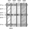
- FIG. 8 is a schematic plan view showing pixels of the liquid crystal display panel of the second embodiment.
- the liquid crystal display panel of Embodiment 2 has a black matrix disposed on the TFT element, on the spacer, and between the picture elements when the panel main surface is viewed in plan. Specifically, each of the picture element in which the yellow color filter 222Y is arranged, the picture element in which the red color filter 222R is arranged, the picture element in which the green color filter 222G is arranged, and the picture element in which the blue color filter 222B is arranged.
- a black matrix 221T is disposed as a TFT light shielding portion.
- a black matrix 221S as a spacer light-shielding portion is arranged. Further, a black matrix 221P as an inter-picture element light shielding portion is arranged.
- an additional black matrix 221A is arranged on the auxiliary capacitance line 211a and the gate line 211b. In the wiring in the liquid crystal display panel of Embodiment 2, 75% or more of the surface area of the metal overlaps with the light shielding layer in the picture element displaying red when the main surface of the panel is viewed in plan.
- the ratio of the additional arrangement is 50% with respect to the conventional metal exposed area in the red picture element, and 30% with respect to the conventional metal exposed area in the yellow picture element.
- the width of the additional black matrix 221A is smaller than the width of the auxiliary capacitance line 211a and the width of the gate line 211b.
- Y: R: G: B 1...
- the spectral reflectance of the copper wiring used in the liquid crystal display panel of Embodiment 2 is the same as the spectral reflectance of the copper wiring shown in FIG.
- FIG. 9 is a graph showing the spectral reflectance of the liquid crystal display panel of the second embodiment.
- R picture element red picture element
- Y picture element yellow picture element
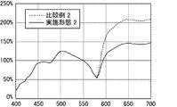
- FIG. 10 is a graph showing the spectral reflectance of the liquid crystal display panel of Embodiment 2 and the spectral reflectance of the liquid crystal display panel of Comparative Example 2 when the reflectance at a wavelength of 550 nm is 100%.
- the reflectance on the display surface side at a wavelength of 600 to 700 nm is 150% or less with respect to the reflectance on the display surface side at a wavelength of 550 nm.
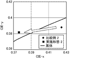
- FIG. 11 is a graph showing the reflected light chromaticity of the liquid crystal display panel of Embodiment 2 and the reflected light chromaticity of the liquid crystal display panel of Comparative Example 2.
- a black matrix is arranged in a part of the exposed portion of the metal wiring on the TFT substrate in the present invention, and the reflectance of 550 nm, which is the central wavelength of white balance obtained by synthesizing each color, is 600.
- the black matrix By additionally arranging the black matrix so that the reflectance in the range of up to 700 nm is 150% or less, the black body locus can be brought close to the chromaticity diagram, and the reddish brown color characteristic of copper wiring is reduced. Therefore, a liquid crystal display device with good display quality can be manufactured.
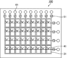
- FIG. 12 is a schematic plan view showing a circuit board in the present embodiment.
- the circuit board 100 is a TFT side substrate provided with a thin film transistor (TFT), and includes a picture element electrode area (display area) and an area outside the picture element electrode area (non-display area).
- the connection part 51 and the terminal part 61 are arranged in the non-display area.
- a source driver can be mounted on the circuit board 100 via the connection unit 51 by, for example, a chip on glass (COG) method.
- COG chip on glass
- a flexible printed circuit board (FPC) can be mounted on the circuit board 100 via the terminal portion 61.
- a signal for driving the source driver can be input from the FPC via the terminal portions 61 and 51.
- a gate wiring and a source wiring are provided on a glass substrate (not shown) so as to be substantially orthogonal to each other, and each region surrounded by the gate wiring and the source wiring is illustrated.
- An elementary electrode 31 and a TFT 41 are provided.
- FIG. 13 is an exploded perspective schematic view showing the structure of the liquid crystal panel in the present embodiment.
- the substrate 72 on the CF side of the liquid crystal panel 200 and the circuit board 100 sandwich the liquid crystal 73.
- the liquid crystal panel 200 includes a backlight 75 on the back surface of the circuit board 100.
- the light of the backlight 75 passes through the polarizing plate 74, the circuit board 100, the liquid crystal 73, the CF-side substrate 72, and the polarizing plate 71 in this order, and the passage / non-transmission of light is controlled by controlling the orientation of the liquid crystal.
- FIG. 14 is an exploded perspective view schematically showing a structure of a liquid crystal display device including the liquid crystal panel shown in FIG.
- the liquid crystal panel 200 is fixed on the fixed panel 400 and sealed by the front cabinet 300 and the rear cabinet 500.
- the rear cabinet 500 and the upper stand 700 are fixed via a metal fitting 600.
- the upper stand 700 and the lower stand 800 are fitted together.
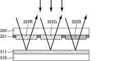
- FIG. 15 is a schematic cross-sectional view showing external light reflection of the liquid crystal display panel of Comparative Example 1.
- the liquid crystal display panel of Comparative Example 1 was obtained by the following (1) to (4).
- (1) As the TFT substrate a substrate disposed on a glass substrate 310 having a copper wiring having a low resistance as a metal wiring 311 was used.
- (2) The color filter substrate used was a substrate in which color filters (322R, 322G, and 322B, respectively) composed of three colors of RGB are arranged on a glass substrate 320.
- the black matrix 321 of the color filter substrate is disposed on the TFT element, on the spacer, and between the picture elements as in the prior art.
- (4) The substrate of (1) and the color filter substrate of (2) were bonded together, and liquid crystal was sealed to form a liquid crystal display device.
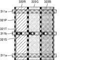
- FIG. 16 is a schematic plan view showing pixels of the liquid crystal display panel of Comparative Example 1.
- a black matrix is arranged only on the TFT elements, on the spacers, and between the picture elements.
- a black matrix 321T as a TFT light shielding unit
- a black matrix 321S is disposed as a spacer light-shielding portion.
- a black matrix 321P as an inter-picture element light-shielding portion is arranged.
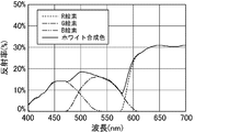
- FIG. 17 is a graph showing the spectral reflectance of the liquid crystal display panel of Comparative Example 1.
- the copper color (reddish brown) unique to copper is emphasized by the R color filter (also called the R colored layer), and the display quality when external light is incident is reduced. It was.
- FIG. 18 is a schematic plan view showing pixels of the liquid crystal display panel of Comparative Example 2.
- the liquid crystal display panel of Comparative Example 2 has a black matrix disposed on the TFT element, on the spacer, and between the picture elements when the panel main surface is viewed in plan. Specifically, each of the picture element in which the yellow color filter 422Y is arranged, the picture element in which the red color filter 422R is arranged, the picture element in which the green color filter 422G is arranged, and the picture element in which the blue color filter 422B is arranged. , A black matrix 421T as a TFT light shielding portion is disposed. Further, in the picture element in which the yellow color filter 422Y is arranged, a black matrix 421S as a spacer light shielding portion is arranged. Further, a black matrix 221P as an inter-picture element light shielding portion is arranged.
- FIG. 19 is a graph showing the spectral reflectance of the liquid crystal display panel of Comparative Example 2.
- the copper color (red brown) unique to copper is emphasized by the R color filter, and the display quality at the time of incident external light is reduced.
Landscapes
- Physics & Mathematics (AREA)
- Nonlinear Science (AREA)
- Mathematical Physics (AREA)
- Chemical & Material Sciences (AREA)
- Crystallography & Structural Chemistry (AREA)
- General Physics & Mathematics (AREA)
- Optics & Photonics (AREA)
- Engineering & Computer Science (AREA)
- Microelectronics & Electronic Packaging (AREA)
- Liquid Crystal (AREA)
Abstract
本発明は、色付きが低減されたり、明室コントラストが向上された液晶表示パネル及び液晶表示装置を提供する。本発明の液晶表示パネルは、可視光領域内に反射率90%以上の波長領域をもつ金属から構成される配線を有する液晶表示パネルであって、上記液晶表示パネルは、波長550nmでの表示面側の反射率に対して、波長600~700nmでの表示面側の反射率が150%以下である液晶表示パネルである。
Description
本発明は、液晶表示パネル及び液晶表示装置に関する。より詳しくは、多色化、高精細化に好適な液晶表示パネル及び液晶表示装置に関するものである。
液晶表示装置は、軽量・薄型・低消費電力を実現することができる表示装置として注目され、モバイル用途や各種のモニター、大型テレビ等、日常生活やビジネスに欠かすことのできないものとなっている。中でも、画素スイッチング素子(駆動素子)として薄膜トランジスタ(TFT)を用いたアクティブマトリクス方式の液晶表示装置は、コントラスト比が高く、応答速度が速い等によって、その市場規模が大きく伸びている。このような液晶表示装置においては、更なるニーズの拡大や技術の進展にともなって、多色化、高精細化等、その画質や表示品位等に関する高性能化、種々の高機能化についての研究開発が益々盛んである。
従来の液晶表示装置としては、2枚の透明基板の間に液晶を封入した構造を有し、それらの透明基板の相互に対向する2つの面のうち、一方の面側には対向電極、カラーフィルタ及び配向膜等が形成され、他方の面側にはTFT、画素電極(表示電極やコモン電極)及び配向膜等が形成され、更に、複数本のゲートバスラインとそれに交差する複数本のデータバスラインが形成された液晶表示パネルを備えたものが開示されている(例えば、特許文献1参照)。この液晶表示パネルにおいては、実施形態としてデータバスラインと平行に、ブラックマトリクスが形成され、データバスラインの幅が4μmであるのに対して、ブラックマトリクスの幅が8μmに設定されたものが示されている。この他、銅又は銅合金を導電性膜又は導電性ラインとして用いた基板が開示されている(例えば、特許文献2~4参照)。
これまでに作製されてきた液晶表示パネル(LCDパネル)は、開口率を拡大し透過率を向上させる観点から、例えば図16に示されるように、パネル主面を平面視したときに、TFT素子上、スペーサ上、絵素間などの位置にだけブラックマトリクスが配置され、遮光される領域が抑えられたものであった。具体的には、このような形態においては、赤色カラーフィルタ322Rが配置された絵素、緑色カラーフィルタ322Gが配置された絵素及び青色カラーフィルタ322Bが配置された絵素のそれぞれにおいて、TFT遮光部としてのブラックマトリクス321T、スペーサ遮光部としてのブラックマトリクス321Sが配置されている。また、絵素間遮光部としてのブラックマトリクス321Pが配置されている。
一方で、その他の補助容量配線311a上及びゲート配線311b上にはブラックマトリクスは配置されていない構成となっている。そのため、絵素内のTFT基板上メタル配線の露出比率が大きなものとなっていた。
一方で、その他の補助容量配線311a上及びゲート配線311b上にはブラックマトリクスは配置されていない構成となっている。そのため、絵素内のTFT基板上メタル配線の露出比率が大きなものとなっていた。
ところで、LCDパネルの基板上に配置される各種の配線としては、メタル配線(金属配線)が用いられるが、パネルの高性能化にともなって、これまでに用いられていたものよりも更に抵抗値が低く抑えられた低抵抗配線の需要が高まっている。
しかしながら、性能向上を実現できるメタル配線の中には、反射率が高く、そのためパネルに外光が入射した際に、メタル配線の反射によってパネル内で不要な反射が多く生じてしまい、表示品位を低下するという課題があった。すなわち、従来のLCDパネルにおいては、特にTFT基板のように複数種のメタル配線によって構成される場合、基板上のメタル配線の反射光により、外光反射による色付き、明室コントラストの低下が問題となっていた。
しかしながら、性能向上を実現できるメタル配線の中には、反射率が高く、そのためパネルに外光が入射した際に、メタル配線の反射によってパネル内で不要な反射が多く生じてしまい、表示品位を低下するという課題があった。すなわち、従来のLCDパネルにおいては、特にTFT基板のように複数種のメタル配線によって構成される場合、基板上のメタル配線の反射光により、外光反射による色付き、明室コントラストの低下が問題となっていた。
本発明は、上記現状に鑑みてなされたものであり、メタル配線を備え、特にTFT基板のように複数種のメタル配線によって構成される形態において、色付きが低減されたり、明室コントラストが向上された液晶表示パネル及びそのような液晶表示パネルを備えた液晶表示装置を提供することを目的とするものである。
本発明者らは、メタル配線を備えた液晶表示パネル及び液晶表示装置について種々検討したところ、メタル配線の中には、可視光の波長領域における特定波長領域の分光反射率が高く、これによって外光入射にともない、液晶表示パネル内において基板上の反射光が多く生じてしまい、外光反射による色付き、明室コントラストの低下を引き起こしていることを発見した。特にTFT基板のように複数種のメタル配線によって構成される場合や、メタル配線が低抵抗配線である場合に、それが顕著に生じることになる。そのような中、特定の反射率をもつメタル配線を備えた液晶表示パネルにおいて、該パネルにおける波長550nmの反射率に対して、波長600~700nmという特定波長領域の反射率に着目した。そして、当該特定波長領域の反射率が高いと赤茶色の色付きや明室コントラストの低下が生じることを見いだし、これに対して当該特定波長領域の反射率を150%以下と特定することにより、赤茶色の色付きが低減されたり、明室コントラストが向上されることを見いだし、上記課題をみごとに解決することができることに想到し、本発明に到達したものである。
本発明においては、液晶表示パネルにおける特定波長領域の反射率の数値範囲を最適化すること、言い換えれば、従来技術においては認識されていなかった当該反射率を限定するという特定の構成と特定の課題・効果との関連性を見いだしたところに技術的意義を有するものである。
本発明においては、液晶表示パネルにおける特定波長領域の反射率の数値範囲を最適化すること、言い換えれば、従来技術においては認識されていなかった当該反射率を限定するという特定の構成と特定の課題・効果との関連性を見いだしたところに技術的意義を有するものである。
すなわち、本発明は、可視光領域内に反射率90%以上の波長領域をもつ金属から構成される配線を有する液晶表示パネルであって、上記液晶表示パネルは、波長550nmでの表示面側の反射率に対して、波長600~700nmでの表示面側の反射率が150%以下である液晶表示パネルである。
例えば、各絵素のブラックマトリクス等の遮光層(以下、単にブラックマトリクスともいう)で遮光されていない金属の分光反射率において、各色を合成したホワイトバランスの中心波長である550nmの反射率に対して、600~700nmの範囲内の反射率が150%以下となるようにブラックマトリクスを追加配置する形態が好ましい。上記反射率を150%以下とすることにより、液晶表示パネルにおける赤茶色の色付きを充分に低減されたり、明室コントラストを優れたものとすることができる。また、可視光領域内に反射率90%以上の波長領域をもつ金属の特性から、上記反射率の下限値を実質的に0%に近づけることは難しく、そのような観点から、上記反射率の下限値としては、例えば50%以上であることが好ましい形態と言える。より好ましくは、100%以上である。
例えば、各絵素のブラックマトリクス等の遮光層(以下、単にブラックマトリクスともいう)で遮光されていない金属の分光反射率において、各色を合成したホワイトバランスの中心波長である550nmの反射率に対して、600~700nmの範囲内の反射率が150%以下となるようにブラックマトリクスを追加配置する形態が好ましい。上記反射率を150%以下とすることにより、液晶表示パネルにおける赤茶色の色付きを充分に低減されたり、明室コントラストを優れたものとすることができる。また、可視光領域内に反射率90%以上の波長領域をもつ金属の特性から、上記反射率の下限値を実質的に0%に近づけることは難しく、そのような観点から、上記反射率の下限値としては、例えば50%以上であることが好ましい形態と言える。より好ましくは、100%以上である。
反射率の測定条件は、積分球(光をほぼ完全に拡散反射する硫酸バリウムなどの白い塗料で内面を塗布した球)等を使って、試料をあらゆる方向から均等に光を照射し、反射光を一方向から受光する方式により反射率測定を行うことができる。
なお、上記反射率は、表示パネルの表示面側(観者側)に向かって反射された光の反射率を意味する。また、上記反射率の上限値は、表示パネルにおける600~700nmの範囲内の最低反射率が150%以下となっていればよいが、平均反射率が150%以下であることがより好ましい。最も好ましくは、表示パネルにおける600~700nmの範囲内の最高反射率が150%以下となることである。
一方で、上記反射率の下限値は、600~700nmの範囲内の最高反射率が上記下限値を満たす、すなわち上記下限値以上であればよいが、平均反射率が上記下限値を満たすことがより好ましい。最も好ましくは、表示パネルにおける600~700nmの範囲内の最低反射率が上記下限値を満たすことである。
なお、上記反射率は、表示パネルの表示面側(観者側)に向かって反射された光の反射率を意味する。また、上記反射率の上限値は、表示パネルにおける600~700nmの範囲内の最低反射率が150%以下となっていればよいが、平均反射率が150%以下であることがより好ましい。最も好ましくは、表示パネルにおける600~700nmの範囲内の最高反射率が150%以下となることである。
一方で、上記反射率の下限値は、600~700nmの範囲内の最高反射率が上記下限値を満たす、すなわち上記下限値以上であればよいが、平均反射率が上記下限値を満たすことがより好ましい。最も好ましくは、表示パネルにおける600~700nmの範囲内の最低反射率が上記下限値を満たすことである。
本発明の液晶表示パネルにおける金属は、例えば、銀、金、銅又はこれらの合金等が挙げられる。中でも、波長600~700nmでの反射率が90%以上であるものが好適である。より好ましくは、反射率が95%以上である形態である。中でも、上記金属が銅又はその合金であることが好ましい。銅又はその合金をはじめとする特有の色付きを有するメタル配線を用いた液晶表示装置において、カラーフィルタ基板に形成されるブラックマトリクスを部分的に追加配置することにより、メタル配線による色付きをより好適に低減することができる。すなわち、上記反射率が90%以上である形態は、メタル配線の表層部が上記金属から構成される場合に好適に適用されることになり、通常であれば入射光の反射が生じると評価されることになるが、本発明の構成を採用することによって、反射光による不具合を充分に抑制するという効果を充分に得ることができる。
本発明の液晶表示パネル及び液晶表示装置の構成としては、このような構成要素を必須として形成されるものである限り、その他の構成要素により特に限定されるものではない。
本発明の液晶表示パネル及び液晶表示装置における好ましい形態について以下に詳しく説明する。
本発明の液晶表示パネル及び液晶表示装置における好ましい形態について以下に詳しく説明する。
本発明の液晶表示パネルの好ましい形態の一つとして、上記配線は、パネル主面を平面視したときに、赤色を表示する絵素内で該金属における表面積の75%以上が遮光層と重畳している形態が挙げられる。このような形態により、赤茶色の色付きを好適に低減することができる。上記金属の遮光層との重畳割合の上限値は、例えば、100%である。なお、反射率の測定条件は、上述したのと同様である。
上記好ましい形態は、特に、銅又はその合金のように赤色系の特有の色付きを有する低抵抗配線を用いる場合に有効である。また、赤色以外の絵素における開口率をできる限り大きくすると共に、赤色の絵素における赤茶色の色付きという課題を充分に解決するためには、赤色を表示する絵素内においてのみメタル配線の遮光層との重畳割合を増し、ブラックマトリクスを追加配置することが好ましい。
上記好ましい形態は、特に、銅又はその合金のように赤色系の特有の色付きを有する低抵抗配線を用いる場合に有効である。また、赤色以外の絵素における開口率をできる限り大きくすると共に、赤色の絵素における赤茶色の色付きという課題を充分に解決するためには、赤色を表示する絵素内においてのみメタル配線の遮光層との重畳割合を増し、ブラックマトリクスを追加配置することが好ましい。
また、上記好ましい形態においては、TFTを用いたアクティブマトリクス方式の基板の場合、従来の金属露出面積に対して、赤色を表示する絵素内において30%以上金属の遮光層との重畳割合を増し、ブラックマトリクスを追加配置することが好ましい。すなわち、TFT素子上、スペーサ上及び絵素間だけにブラックマトリクスを配置し、その他の箇所の金属が露出している領域の面積に対して、赤色を表示する絵素内において30%以上金属の遮光層との重畳割合を増すことが好ましい。より好ましくは、赤色を表示する絵素内においてのみ30%以上金属の遮光層との重畳割合を増した形態である。これらの場合、ブラックマトリクス面積の追加割合が30%以上ということになる。
なお、金属露出面積とは、液晶表示パネル内において、外光入射の際に金属による反射が生じる領域の面積である。通常、メタル配線は、各種の膜などによって覆われているが、平面視したときにブラックマトリクスなどの遮光層と重畳していない領域においては、反射が生じることになる。本明細書においては、平面視したときにブラックマトリクスなどの遮光層に覆われた構成になっていないという意味で「露出」という用語を用いている。
なお、金属露出面積とは、液晶表示パネル内において、外光入射の際に金属による反射が生じる領域の面積である。通常、メタル配線は、各種の膜などによって覆われているが、平面視したときにブラックマトリクスなどの遮光層と重畳していない領域においては、反射が生じることになる。本明細書においては、平面視したときにブラックマトリクスなどの遮光層に覆われた構成になっていないという意味で「露出」という用語を用いている。
上記形態においては、例えば、赤色を表示する絵素内において、TFT素子上、スペーサ上及び絵素間にブラックマトリクスを配置すると共に、ゲートバスライン及び/又は補助容量配線上の一部にもブラックマトリクスを配置することが好適である。この場合、ゲートバスライン及び補助容量配線の金属露出面積(金属反射領域の面積)の30%以上、好ましくは上記%範囲において、ブラックマトリクスを配置することになる。なお、上記ゲートバスライン及び補助容量配線の金属露出面積は、TFT素子上、スペーサ上及び絵素間に配置されたブラックマトリクスによって既に遮光された面積を除いた部分における金属露出面積である。
上記好ましい形態においては、赤色を表示する絵素における金属の遮光層との重畳割合、金属露出面積を説明したが、赤色(R)、緑色(G)、青色(B)のRGB3原色に加えて、黄色(Y)の絵素を加えたRGBY4原色又はシアン色(C)の絵素を加えたRGBC4原色や、RGBY又はRGBCを必須としたそれ以上の多原色の液晶表示パネルにおいて、赤色を表示する絵素と共に、黄色の絵素及び/又はシアン色の絵素にも適用することが好ましい。これらの形態においては、赤色と、黄色及び/又はシアン色との絵素に対してはブラックマトリクスを追加配置し、それら以外の絵素については、上記形態と同様にブラックマトリクスを追加配置しないようにすることが好ましい。黄色やシアン色の絵素についても、赤色の絵素と同様に金属露出にともなう赤茶色の色付きが生じるからである。
より好ましくは、RGBYを必須とした液晶表示パネルにおいて、赤色を表示する絵素と共に、黄色の絵素にも適用することである。
より好ましくは、RGBYを必須とした液晶表示パネルにおいて、赤色を表示する絵素と共に、黄色の絵素にも適用することである。
例えば、TFT素子上、スペーサ上及び絵素間だけにブラックマトリクスを配置し、その他の箇所の金属が露出している領域の面積に対して、赤色と、黄色及び/又はシアン色との絵素内において、それぞれ30%以上金属の遮光層との重畳割合を増すことが好ましい。より好ましくは、赤色と、黄色及び/又はシアン色との絵素内においてだけ、それぞれ上記のように30%以上金属の遮光層との重畳割合を増した形態である。上記金属の遮光層との重畳割合の上限値は、例えば100%である。
更に、上記4原色以上の形態においては、赤色と、黄色及び/又はシアン色との絵素を必須とする場合、赤色の絵素に追加配置されるブラックマトリクスの追加割合が、黄色及び/又はシアン色の絵素に追加配置されるブラックマトリクス面積の追加割合よりも大きくなるようにすることが好ましい。例えば、赤色の絵素におけるブラックマトリクス面積の追加割合を50%以上とし、黄色及び/又はシアン色の絵素におけるブラックマトリクス面積の追加割合を30%以上、50%未満とすることが好ましい。メタル配線の光反射によるコントラストに与える影響が赤色の絵素の方が黄色やシアン色の絵素よりも大きく、特にその表層部が銅又は銅を含む合金であるメタル配線を用いる場合、赤色の絵素が通常は最も大きいことから赤茶色の色付きによるコントラストの影響を受けることになる。
なお、上記4原色以上の好ましい形態を挙げれば、赤、緑、青及び黄のサブ画素を有する画素によって表示面が構成された表示装置であって、赤及び/又は青のサブ画素は、他のサブ画素よりも開口面積が大きい形態(他のサブ画素よりも、赤のサブ画素の開口面積が最大である形態、青のサブ画素の開口面積が最大である形態、赤及び青のサブ画素の開口面積が共に最大である形態)、緑及び/又は黄のサブ画素は、他のサブ画素よりも開口面積が小さい形態(他のサブ画素よりも、緑のサブ画素の開口面積が最小である形態、黄のサブ画素の開口面積が最小である形態、緑及び黄のサブ画素の開口面積が共に最小である形態)が挙げられる。同様に、黄をシアンに置き換えることができる。また、黄及びシアンを同時に有していてもよい。更に、上記画素は、色特性が互いに異なる赤及び/又は青のサブ画素を有する形態も挙げられる。
これら4原色又は4原色以上の液晶表示装置においては、表示に用いる原色の数を増やすことにより、特に赤色の明度の低下によって、視認性が損なわれることになる。また、白表示の色調を調節するために、高色温度の光源が用いられると、赤表示の明度は更に低下し、これに伴って、視認性は更に損なわれる。上記好ましい形態とすれば、明るい赤を表示することができる結果、視認性を向上させることができ、それによって本発明の構成と相まって、外光反射による色付きを低減したり、明室コントラストの低下を抑制するという本発明の効果を得ることができる。
これら4原色又は4原色以上の液晶表示装置においては、表示に用いる原色の数を増やすことにより、特に赤色の明度の低下によって、視認性が損なわれることになる。また、白表示の色調を調節するために、高色温度の光源が用いられると、赤表示の明度は更に低下し、これに伴って、視認性は更に損なわれる。上記好ましい形態とすれば、明るい赤を表示することができる結果、視認性を向上させることができ、それによって本発明の構成と相まって、外光反射による色付きを低減したり、明室コントラストの低下を抑制するという本発明の効果を得ることができる。
また、本発明の液晶表示パネルの好ましい形態としては、上記配線は、パネル主面を平面視したときに、少なくとも一部が該配線と略同一の幅か及び/又は該配線より狭い幅の遮光層と重畳している形態が挙げられる。より好ましくは、該配線より狭い幅の遮光層と重畳している形態である。通常では、メタル配線をブラックマトリクスで覆うのであれば、生産時の誤差なども考慮してメタル配線の幅よりもブラックマトリクスの幅を少し大きくして配置することになるが、本形態においては、メタル配線の光反射によるコントラストの低下を抑えたり、開口率の向上による透過率の向上する効果を充分に得ることができる。
このような形態により、遮光割合を好ましく調整した上で、色味を制御することができる。
なお、メタル配線の少なくとも一部が該配線と略同一の幅か及び/又は該配線より狭い幅の遮光層と重畳するようにするのは、上述したブラックマトリクスを追加配置する好ましい形態において、追加配置されるブラックマトリクスに適用することが好ましい。従って、赤色を表示する絵素内において、赤色に加えて黄色及び/又はシアン色を表示する絵素がある場合には、赤色と、黄色及び/又はシアン色とを表示する絵素内において、TFT素子上、スペーサ上及び絵素間にブラックマトリクスを配置すると共に、ゲートバスライン及び/又は補助容量配線上の一部にもブラックマトリクスを配置し、該ゲートバスライン及び/又は補助容量配線の少なくとも一部が該配線と略同一の幅か及び/又は該配線より狭い幅のブラックマトリクスと重畳している形態とすることが好適である。この場合も、より好ましくは、RGBYを必須とした液晶表示パネルにおいて、赤色を表示する絵素と共に、黄色の絵素にも適用することである。また、より好ましくは、該配線より狭い幅の遮光層と重畳している形態である。更に、上記配線は、その表層部が銅又は銅を含む合金である形態であれば、そのようなメタル配線を用いることによる低抵抗という有利な点を生かしつつ、赤茶色の色付きを好適に低減することができ、これらの相乗的な効果を得ることができる。
このような形態により、遮光割合を好ましく調整した上で、色味を制御することができる。
なお、メタル配線の少なくとも一部が該配線と略同一の幅か及び/又は該配線より狭い幅の遮光層と重畳するようにするのは、上述したブラックマトリクスを追加配置する好ましい形態において、追加配置されるブラックマトリクスに適用することが好ましい。従って、赤色を表示する絵素内において、赤色に加えて黄色及び/又はシアン色を表示する絵素がある場合には、赤色と、黄色及び/又はシアン色とを表示する絵素内において、TFT素子上、スペーサ上及び絵素間にブラックマトリクスを配置すると共に、ゲートバスライン及び/又は補助容量配線上の一部にもブラックマトリクスを配置し、該ゲートバスライン及び/又は補助容量配線の少なくとも一部が該配線と略同一の幅か及び/又は該配線より狭い幅のブラックマトリクスと重畳している形態とすることが好適である。この場合も、より好ましくは、RGBYを必須とした液晶表示パネルにおいて、赤色を表示する絵素と共に、黄色の絵素にも適用することである。また、より好ましくは、該配線より狭い幅の遮光層と重畳している形態である。更に、上記配線は、その表層部が銅又は銅を含む合金である形態であれば、そのようなメタル配線を用いることによる低抵抗という有利な点を生かしつつ、赤茶色の色付きを好適に低減することができ、これらの相乗的な効果を得ることができる。
更に、本発明の好ましい形態としては、上述した本発明の形態及び好ましい形態を、薄膜トランジスタ(TFT)を用いたアクティブマトリクス方式の基板を備える液晶表示パネルに適用することである。この場合、液晶表示パネルを構成する透明基板上にゲートバスラインを備えることが好ましい。より好ましくは、ゲートバスライン及び補助容量配線を備えることである。
本発明はまた、本発明の液晶表示パネルを備える液晶表示装置でもある。これによって、色付きが低減されたり、明室コントラストに優れた液晶表示装置とすることができる。
本発明はまた、本発明の液晶表示パネルを備える液晶表示装置でもある。これによって、色付きが低減されたり、明室コントラストに優れた液晶表示装置とすることができる。
上述した各形態は、本発明の要旨を逸脱しない範囲において適宜組み合わされてもよい。
本発明の液晶表示パネル及び液晶表示装置によれば、色付きが低減されたり、明室コントラストが向上されたものとすることができる。
本明細書において、回路基板は、実施形態においてTFTが設けられる基板であることから、TFT側基板ともいう。上記回路基板に対向する基板は、実施形態においてカラーフィルタ(CF)が配置される基板であることから、CF側基板ともいう。また、表層部とは、表示パネルの表示面側の層部分をいう。
以下に実施形態を掲げ、本発明を図面を参照して更に詳細に説明するが、本発明はこれらの実施形態のみに限定されるものではない。なお、反射率の測定は、積分球(光をほぼ完全に拡散反射する硫酸バリウムなどの白い塗料で内面を塗布した球)を使って、試料をあらゆる方向から均等に光を照射し、反射光を一方向から受光する方式により行った。
(実施形態1)
実施形態1の液晶表示パネルは、以下の(1)~(4)により得られたものである。なお、特にこの手順に限定されるものではない。(1)TFT基板は低抵抗配線である銅配線をメタル配線とした基板を用いた。また、銅の合金も好適に用いることができる。実施形態1の液晶表示パネルは、ゲート配線、補助容量配線及びソース配線の表層のすべてが高反射率配線(銅配線)となっているが、高反射率の金属を配線表層部の一部に使用するものであってもよく、例えばゲート配線表層部だけが高反射率配線である形態であってもよい。上記メタル配線の表面状態は、反射率の特定を満たす限り、平坦であってもよく、凹凸があってもよい。なお、表層が高反射率配線である形態とは、高反射率配線上に透明電極が形成された形態等の、高反射率配線が表層に露出した形態も含むものである。(2)カラーフィルタ基板はR(赤)G(緑)B(青)の3色で構成されるものを用いた。(3)カラーフィルタ基板のブラックマトリクスは、従来のTFT素子上、スペーサ上、絵素間に加えて、R絵素のみにブラックマトリクスを追加配置した。従来の金属露出面積に対して、R絵素のみに30%のブラックマトリクスを追加して配置した。(4)上記(1)の基板と(2)のカラーフィルタ基板とを貼り合せ、液晶を封入することで液晶表示装置を形成した。
実施形態1の液晶表示パネルは、以下の(1)~(4)により得られたものである。なお、特にこの手順に限定されるものではない。(1)TFT基板は低抵抗配線である銅配線をメタル配線とした基板を用いた。また、銅の合金も好適に用いることができる。実施形態1の液晶表示パネルは、ゲート配線、補助容量配線及びソース配線の表層のすべてが高反射率配線(銅配線)となっているが、高反射率の金属を配線表層部の一部に使用するものであってもよく、例えばゲート配線表層部だけが高反射率配線である形態であってもよい。上記メタル配線の表面状態は、反射率の特定を満たす限り、平坦であってもよく、凹凸があってもよい。なお、表層が高反射率配線である形態とは、高反射率配線上に透明電極が形成された形態等の、高反射率配線が表層に露出した形態も含むものである。(2)カラーフィルタ基板はR(赤)G(緑)B(青)の3色で構成されるものを用いた。(3)カラーフィルタ基板のブラックマトリクスは、従来のTFT素子上、スペーサ上、絵素間に加えて、R絵素のみにブラックマトリクスを追加配置した。従来の金属露出面積に対して、R絵素のみに30%のブラックマトリクスを追加して配置した。(4)上記(1)の基板と(2)のカラーフィルタ基板とを貼り合せ、液晶を封入することで液晶表示装置を形成した。
図1は、実施形態1の液晶表示パネルの画素を示す平面模式図である。
実施形態1の液晶表示パネルは、図1に示されるように、パネル主面を平面視したときに、TFT素子上、スペーサ上、絵素間にそれぞれブラックマトリクスが配置されている。具体的には、赤色カラーフィルタ22Rが配置された絵素、緑色カラーフィルタ22Gが配置された絵素及び青色カラーフィルタ22Bが配置された絵素のそれぞれにおいて、TFT遮光部としてのブラックマトリクス21T、スペーサ遮光部としてのブラックマトリクス21Sが配置されている。また、絵素間遮光部としてのブラックマトリクス21Pが配置されている。更に、赤色カラーフィルタ22Rが配置された絵素においてのみ、補助容量配線11a及びゲート配線11b上に追加のブラックマトリクス21Aが配置されている。実施形態1の液晶表示パネルにおける配線は、パネル主面を平面視したときに、赤色を表示する絵素内で該金属における表面積の75%以上が遮光層と重畳している。追加配置された割合は、赤色絵素内の従来の金属露出面積に対して30%である。追加のブラックマトリクス21Aは、その幅が補助容量配線11aの幅及びゲート配線11bの幅よりも狭いものである。
実施形態1の液晶表示パネルは、図1に示されるように、パネル主面を平面視したときに、TFT素子上、スペーサ上、絵素間にそれぞれブラックマトリクスが配置されている。具体的には、赤色カラーフィルタ22Rが配置された絵素、緑色カラーフィルタ22Gが配置された絵素及び青色カラーフィルタ22Bが配置された絵素のそれぞれにおいて、TFT遮光部としてのブラックマトリクス21T、スペーサ遮光部としてのブラックマトリクス21Sが配置されている。また、絵素間遮光部としてのブラックマトリクス21Pが配置されている。更に、赤色カラーフィルタ22Rが配置された絵素においてのみ、補助容量配線11a及びゲート配線11b上に追加のブラックマトリクス21Aが配置されている。実施形態1の液晶表示パネルにおける配線は、パネル主面を平面視したときに、赤色を表示する絵素内で該金属における表面積の75%以上が遮光層と重畳している。追加配置された割合は、赤色絵素内の従来の金属露出面積に対して30%である。追加のブラックマトリクス21Aは、その幅が補助容量配線11aの幅及びゲート配線11bの幅よりも狭いものである。
実施形態1におけるカラーフィルタの色配列は、図1に示されるようにRGBの繰り返し配列であり、その面積比率は1.0:1.0:1.0とした。
図2は、実施形態1の液晶表示パネルのソース配線を示す部分拡大図である。
ソース配線13Sがジクザク状に配置され、パネル主面を平面視したときに、ソース配線13Sの一部が赤色絵素内にあり、他の一部は赤色絵素以外の絵素内(例えば、青色絵素内)にある。このとき、少なくとも赤色絵素内のソース配線13Sと重畳するようにブラックマトリクスを配置することが好ましい。より好ましくは、透過率の観点から、赤色絵素内においてだけソース配線13Sと重畳するようにブラックマトリクスを配置する形態である。
ソース配線13Sがジクザク状に配置され、パネル主面を平面視したときに、ソース配線13Sの一部が赤色絵素内にあり、他の一部は赤色絵素以外の絵素内(例えば、青色絵素内)にある。このとき、少なくとも赤色絵素内のソース配線13Sと重畳するようにブラックマトリクスを配置することが好ましい。より好ましくは、透過率の観点から、赤色絵素内においてだけソース配線13Sと重畳するようにブラックマトリクスを配置する形態である。
図3は、銅配線、アルミニウム配線及びチタン配線の分光反射率を示すグラフである。
言い換えれば、図3には、本実施形態の液晶表示パネルに用いた銅配線の分光反射率が示されている。図3に示されるように、銅配線は、波長590~700nmの範囲内において反射率が90%以上となっている。一方、アルミニウム配線及びチタン配線は、可視光領域において反射率は90%未満であり、これらは銅配線ほど低抵抗ではないものの、色付きの程度はもともと小さかったものである。
言い換えれば、図3には、本実施形態の液晶表示パネルに用いた銅配線の分光反射率が示されている。図3に示されるように、銅配線は、波長590~700nmの範囲内において反射率が90%以上となっている。一方、アルミニウム配線及びチタン配線は、可視光領域において反射率は90%未満であり、これらは銅配線ほど低抵抗ではないものの、色付きの程度はもともと小さかったものである。
図4は、実施形態1の液晶表示パネルの分光反射率を示すグラフである。
このように、赤色絵素(R絵素)のみにブラックマトリクスを追加配置させることで、600~700nmの波長域の反射率を抑えることが可能となる。
このように、赤色絵素(R絵素)のみにブラックマトリクスを追加配置させることで、600~700nmの波長域の反射率を抑えることが可能となる。
図5は、波長550nmにおける反射率を100%としたときの、実施形態1の液晶表示パネルの分光反射率及び比較例1の液晶表示パネルの分光反射率を示すグラフである。
実施形態1の液晶表示パネルは、波長550nmでの表示面側の反射率に対して、波長600~700nmでの表示面側の反射率が150%以下である。
実施形態1の液晶表示パネルは、波長550nmでの表示面側の反射率に対して、波長600~700nmでの表示面側の反射率が150%以下である。
図6は、実施形態1の液晶表示パネルの反射光色度及び比較例1の液晶表示パネルの反射光色度を示すグラフである。なお、図6は、XYZ表色系で示されたものである。図6中「黒体」とは、xy色度図上の黒体軌跡を示す。図6のグラフ中、右側ほど赤色がかっていることになり、左側ほど青色がかっていることになり、上側ほど緑色がかっていることになる。図11においても同様である。
実施形態1の液晶表示パネルでは、TFT基板上メタル配線露出部の一部にブラックマトリクスを配置し、かつ各色を合成したホワイトバランスの中心波長である550nmの反射率に対して、600~700nmの範囲内の反射率が150%以下となる様にブラックマトリクスを追加配置することで、色度図上で黒体軌跡に近づけることができ、銅配線特有の赤茶色の色付きを低減することが可能となり、表示品位の良好な液晶表示装置を作製することができる。
実施形態1の液晶表示パネルでは、TFT基板上メタル配線露出部の一部にブラックマトリクスを配置し、かつ各色を合成したホワイトバランスの中心波長である550nmの反射率に対して、600~700nmの範囲内の反射率が150%以下となる様にブラックマトリクスを追加配置することで、色度図上で黒体軌跡に近づけることができ、銅配線特有の赤茶色の色付きを低減することが可能となり、表示品位の良好な液晶表示装置を作製することができる。
図7は、実施形態1の変形例の液晶表示パネルの画素を示す平面模式図である。
実施形態1の変形例の液晶表示パネルは、図7に示されるように、パネル主面を平面視したときに、TFT素子上、スペーサ上、絵素間にそれぞれブラックマトリクスが配置されている。具体的には、赤色カラーフィルタ122Rが配置された絵素、緑色カラーフィルタ122Gが配置された絵素及び青色カラーフィルタ122Bが配置された絵素のそれぞれにおいて、TFT遮光部としてのブラックマトリクス121T、スペーサ遮光部としてのブラックマトリクス121Sが配置されている。また、絵素間遮光部としてのブラックマトリクス121Pが配置されている。更に、補助容量配線111a及びゲート配線111b上に追加のブラックマトリクス121Aが配置されている。追加のブラックマトリクス121Aは、その幅が補助容量配線111aの幅及びゲート配線111bの幅よりも狭いものである。このような液晶表示パネルによっても、色付きを低減することが可能となり、表示品位の良好な液晶表示装置を作製することができる。
実施形態1の変形例の液晶表示パネルは、図7に示されるように、パネル主面を平面視したときに、TFT素子上、スペーサ上、絵素間にそれぞれブラックマトリクスが配置されている。具体的には、赤色カラーフィルタ122Rが配置された絵素、緑色カラーフィルタ122Gが配置された絵素及び青色カラーフィルタ122Bが配置された絵素のそれぞれにおいて、TFT遮光部としてのブラックマトリクス121T、スペーサ遮光部としてのブラックマトリクス121Sが配置されている。また、絵素間遮光部としてのブラックマトリクス121Pが配置されている。更に、補助容量配線111a及びゲート配線111b上に追加のブラックマトリクス121Aが配置されている。追加のブラックマトリクス121Aは、その幅が補助容量配線111aの幅及びゲート配線111bの幅よりも狭いものである。このような液晶表示パネルによっても、色付きを低減することが可能となり、表示品位の良好な液晶表示装置を作製することができる。
(実施形態2)
実施形態2の液晶表示パネルは、以下の(1)~(4)により得られたものである。なお、特にこの手順に限定されるものではない。(1)TFT基板は低抵抗配線である銅配線をメタル配線とした基板を用いた。また、銅の合金も好適に用いることができる。実施形態2の液晶表示パネルは、ゲート配線、補助容量配線及びソース配線のすべてが高反射率配線(銅配線)となっているが、高反射率の金属を配線表層部の一部に使用するものであってもよく、例えばゲート配線表層部だけが高反射率配線である形態であってもよい。上記メタル配線の表面状態は、反射率の特定を満たす限り、平坦であってもよく、凹凸があってもよい。なお、表層が高反射率配線である形態とは、高反射率配線上に透明電極が形成された形態等の、高反射率配線が表層に露出した形態も含むものである。(2)カラーフィルタ基板はRGBで構成されるカラーフィルタに対しY(黄色)を加えた4色構成とした。(3)カラーフィルタ基板のブラックマトリクスは、従来のTFT素子上、スペーサ上、絵素間に加えて、R絵素とY絵素にブラックマトリクスを追加配置した。従来の金属露出面積に対して、R絵素に50%のブラックマトリクス、Y絵素に30%のブラックマトリクスをそれぞれ追加して配置した。(4)上記(1)の基板と(2)のカラーフィルタ基板とを貼り合せ、液晶を封入することで液晶表示装置を形成した。
実施形態2の液晶表示パネルは、以下の(1)~(4)により得られたものである。なお、特にこの手順に限定されるものではない。(1)TFT基板は低抵抗配線である銅配線をメタル配線とした基板を用いた。また、銅の合金も好適に用いることができる。実施形態2の液晶表示パネルは、ゲート配線、補助容量配線及びソース配線のすべてが高反射率配線(銅配線)となっているが、高反射率の金属を配線表層部の一部に使用するものであってもよく、例えばゲート配線表層部だけが高反射率配線である形態であってもよい。上記メタル配線の表面状態は、反射率の特定を満たす限り、平坦であってもよく、凹凸があってもよい。なお、表層が高反射率配線である形態とは、高反射率配線上に透明電極が形成された形態等の、高反射率配線が表層に露出した形態も含むものである。(2)カラーフィルタ基板はRGBで構成されるカラーフィルタに対しY(黄色)を加えた4色構成とした。(3)カラーフィルタ基板のブラックマトリクスは、従来のTFT素子上、スペーサ上、絵素間に加えて、R絵素とY絵素にブラックマトリクスを追加配置した。従来の金属露出面積に対して、R絵素に50%のブラックマトリクス、Y絵素に30%のブラックマトリクスをそれぞれ追加して配置した。(4)上記(1)の基板と(2)のカラーフィルタ基板とを貼り合せ、液晶を封入することで液晶表示装置を形成した。
図8は、実施形態2の液晶表示パネルの画素を示す平面模式図である。
実施形態2の液晶表示パネルは、図8に示されるように、パネル主面を平面視したときに、TFT素子上、スペーサ上、絵素間にそれぞれブラックマトリクスが配置されている。具体的には、黄色カラーフィルタ222Yが配置された絵素、赤色カラーフィルタ222Rが配置された絵素、緑色カラーフィルタ222Gが配置された絵素及び青色カラーフィルタ222Bが配置された絵素のそれぞれにおいて、TFT遮光部としてのブラックマトリクス221Tが配置されている。また、黄色カラーフィルタ222Yが配置された絵素において、スペーサ遮光部としてのブラックマトリクス221Sが配置されている。更に、絵素間遮光部としてのブラックマトリクス221Pが配置されている。そして、黄色カラーフィルタ222Yが配置された絵素及び赤色カラーフィルタ222Rが配置された絵素において、補助容量配線211a及びゲート配線211b上に追加のブラックマトリクス221Aが配置されている。実施形態2の液晶表示パネルにおける配線は、パネル主面を平面視したときに、赤色を表示する絵素内で該金属における表面積の75%以上が遮光層と重畳している。追加配置された割合は、赤色絵素内では従来の金属露出面積に対して50%であり、黄色絵素内では従来の金属露出面積に対して30%である。追加のブラックマトリクス221Aの幅は、補助容量配線211aの幅及びゲート配線211bの幅よりも狭いものである。
実施形態2の液晶表示パネルは、図8に示されるように、パネル主面を平面視したときに、TFT素子上、スペーサ上、絵素間にそれぞれブラックマトリクスが配置されている。具体的には、黄色カラーフィルタ222Yが配置された絵素、赤色カラーフィルタ222Rが配置された絵素、緑色カラーフィルタ222Gが配置された絵素及び青色カラーフィルタ222Bが配置された絵素のそれぞれにおいて、TFT遮光部としてのブラックマトリクス221Tが配置されている。また、黄色カラーフィルタ222Yが配置された絵素において、スペーサ遮光部としてのブラックマトリクス221Sが配置されている。更に、絵素間遮光部としてのブラックマトリクス221Pが配置されている。そして、黄色カラーフィルタ222Yが配置された絵素及び赤色カラーフィルタ222Rが配置された絵素において、補助容量配線211a及びゲート配線211b上に追加のブラックマトリクス221Aが配置されている。実施形態2の液晶表示パネルにおける配線は、パネル主面を平面視したときに、赤色を表示する絵素内で該金属における表面積の75%以上が遮光層と重畳している。追加配置された割合は、赤色絵素内では従来の金属露出面積に対して50%であり、黄色絵素内では従来の金属露出面積に対して30%である。追加のブラックマトリクス221Aの幅は、補助容量配線211aの幅及びゲート配線211bの幅よりも狭いものである。
実施形態2におけるカラーフィルタの色配列は、図8に示されるようにYRGBの繰り返し配列であり、その面積比率は、色再現性とホワイトバランス調整のため、Y:R:G:B=1.0:1.6:1.0:1.6とした。
実施形態2の液晶表示パネルに用いた銅配線の分光反射率は、図3に示した銅配線の分光反射率と同様である。
図9は、実施形態2の液晶表示パネルの分光反射率を示すグラフである。
このように、赤色絵素(R絵素)及び黄色絵素(Y絵素)にブラックマトリクスを追加配置させることで、600~700nmの波長域の反射率を抑えることが可能となる。
このように、赤色絵素(R絵素)及び黄色絵素(Y絵素)にブラックマトリクスを追加配置させることで、600~700nmの波長域の反射率を抑えることが可能となる。
図10は、波長550nmにおける反射率を100%としたときの、実施形態2の液晶表示パネルの分光反射率及び比較例2の液晶表示パネルの分光反射率を示すグラフである。
実施形態2の液晶表示パネルは、波長550nmでの表示面側の反射率に対して、波長600~700nmでの表示面側の反射率が150%以下である。
実施形態2の液晶表示パネルは、波長550nmでの表示面側の反射率に対して、波長600~700nmでの表示面側の反射率が150%以下である。
図11は、実施形態2の液晶表示パネルの反射光色度及び比較例2の液晶表示パネルの反射光色度を示すグラフである。
実施形態2の液晶表示パネルでは、本発明におけるTFT基板上メタル配線露出部の一部にブラックマトリクスを配置し、かつ各色を合成したホワイトバランスの中心波長である550nmの反射率に対して、600~700nmの範囲内の反射率が150%以下となる様にブラックマトリクスを追加配置することで、色度図上で黒体軌跡に近づけることができ、銅配線特有の赤茶色の色付きを低減することが可能となり、表示品位の良好な液晶表示装置を作製することができる。
実施形態2の液晶表示パネルでは、本発明におけるTFT基板上メタル配線露出部の一部にブラックマトリクスを配置し、かつ各色を合成したホワイトバランスの中心波長である550nmの反射率に対して、600~700nmの範囲内の反射率が150%以下となる様にブラックマトリクスを追加配置することで、色度図上で黒体軌跡に近づけることができ、銅配線特有の赤茶色の色付きを低減することが可能となり、表示品位の良好な液晶表示装置を作製することができる。
上述したように、本実施形態では、金属露出面積を低減することにより、色味を好適に制御することができる。
図12は、本実施形態における回路基板を示す平面模式図である。
回路基板100は、薄膜トランジスタ(TFT)が設けられたTFT側基板であり、絵素電極エリア(表示領域)と絵素電極エリアの外側の領域(非表示領域)とを備える。
非表示領域には、接続部51及び端子部61が配置されている。接続部51を介して、ソースドライバを、例えばチップオングラス(COG)方式で回路基板100上に実装することができる。また、端子部61を介して、フレキシブルプリント基板(FPC)を回路基板100上に実装することができる。例えば、FPCから端子部61及び51を介してソースドライバを駆動するための信号を入力することができる。
なお、回路基板100の表示領域には、ガラス基板(示さず)上に、ゲート配線とソース配線とが略直交するように設けられ、更に、ゲート配線とソース配線とで囲まれる領域ごとに絵素電極31及びTFT41が設けられている。
回路基板100は、薄膜トランジスタ(TFT)が設けられたTFT側基板であり、絵素電極エリア(表示領域)と絵素電極エリアの外側の領域(非表示領域)とを備える。
非表示領域には、接続部51及び端子部61が配置されている。接続部51を介して、ソースドライバを、例えばチップオングラス(COG)方式で回路基板100上に実装することができる。また、端子部61を介して、フレキシブルプリント基板(FPC)を回路基板100上に実装することができる。例えば、FPCから端子部61及び51を介してソースドライバを駆動するための信号を入力することができる。
なお、回路基板100の表示領域には、ガラス基板(示さず)上に、ゲート配線とソース配線とが略直交するように設けられ、更に、ゲート配線とソース配線とで囲まれる領域ごとに絵素電極31及びTFT41が設けられている。
図13は、本実施形態における液晶パネルの構造を示す分解斜視模式図である。図13に示されるように、液晶パネル200のCF側の基板72と回路基板100とは液晶73を挟持する。また、液晶パネル200は、回路基板100の背面に、バックライト75を備える。バックライト75の光は、偏光板74、回路基板100、液晶73、CF側の基板72、及び、偏光板71をこの順に通過し、液晶の配向制御により光の通過・非透過を制御する。
図14は、図13に示した液晶パネルを備える液晶表示装置の構造を示す分解斜視模式図である。図14に示されるように、液晶パネル200は、固定パネル400上に固定され、前部キャビネット300及び後部キャビネット500により封じられる。そして、後部キャビネット500と上部スタンド700とが金具600を介して固定される。また上部スタンド700と下部スタンド800とが嵌め合わせされる。
(比較例1)
図15は、比較例1の液晶表示パネルの外光反射を示す断面模式図である。
比較例1の液晶表示パネルは、以下の(1)~(4)により得られたものである。(1)TFT基板は低抵抗である銅配線をメタル配線311としたガラス基板310上に配置した基板を用いた。(2)カラーフィルタ基板はRGBの3色で構成されるカラーフィルタ(それぞれ、322R、322G、322B)をガラス基板320上に配置した基板を用いた。(3)カラーフィルタ基板のブラックマトリクス321は、従来のようにTFT素子上、スペーサ上、絵素間に配置した。(4)上記(1)の基板と(2)のカラーフィルタ基板とを貼り合せ、液晶を封入することで液晶表示装置を形成した。
図15は、比較例1の液晶表示パネルの外光反射を示す断面模式図である。
比較例1の液晶表示パネルは、以下の(1)~(4)により得られたものである。(1)TFT基板は低抵抗である銅配線をメタル配線311としたガラス基板310上に配置した基板を用いた。(2)カラーフィルタ基板はRGBの3色で構成されるカラーフィルタ(それぞれ、322R、322G、322B)をガラス基板320上に配置した基板を用いた。(3)カラーフィルタ基板のブラックマトリクス321は、従来のようにTFT素子上、スペーサ上、絵素間に配置した。(4)上記(1)の基板と(2)のカラーフィルタ基板とを貼り合せ、液晶を封入することで液晶表示装置を形成した。
図16は、比較例1の液晶表示パネルの画素を示す平面模式図である。
比較例1の液晶表示パネルは、図16に示されるように、パネル主面を平面視したときに、TFT素子上、スペーサ上、絵素間だけにそれぞれブラックマトリクスが配置されている。具体的には、赤色カラーフィルタ322Rが配置された絵素、緑色カラーフィルタ322Gが配置された絵素及び青色カラーフィルタ322Bが配置された絵素のそれぞれにおいて、TFT遮光部としてのブラックマトリクス321T、スペーサ遮光部としてのブラックマトリクス321Sが配置されている。また、絵素間遮光部としてのブラックマトリクス321Pが配置されている。
比較例1の液晶表示パネルは、図16に示されるように、パネル主面を平面視したときに、TFT素子上、スペーサ上、絵素間だけにそれぞれブラックマトリクスが配置されている。具体的には、赤色カラーフィルタ322Rが配置された絵素、緑色カラーフィルタ322Gが配置された絵素及び青色カラーフィルタ322Bが配置された絵素のそれぞれにおいて、TFT遮光部としてのブラックマトリクス321T、スペーサ遮光部としてのブラックマトリクス321Sが配置されている。また、絵素間遮光部としてのブラックマトリクス321Pが配置されている。
図17は、比較例1の液晶表示パネルの分光反射率を示すグラフである。
低抵抗配線である銅を用いたTFT基板では、銅特有の銅色(赤茶色)の色付きがRカラーフィルタ(R着色層ともいう)により強調され、外光入射時の表示品位が低下していた。
低抵抗配線である銅を用いたTFT基板では、銅特有の銅色(赤茶色)の色付きがRカラーフィルタ(R着色層ともいう)により強調され、外光入射時の表示品位が低下していた。
(比較例2)
図18は、比較例2の液晶表示パネルの画素を示す平面模式図である。
比較例2の液晶表示パネルは、図18に示されるように、パネル主面を平面視したときに、TFT素子上、スペーサ上、絵素間にそれぞれブラックマトリクスが配置されている。具体的には、黄色カラーフィルタ422Yが配置された絵素、赤色カラーフィルタ422Rが配置された絵素、緑色カラーフィルタ422Gが配置された絵素及び青色カラーフィルタ422Bが配置された絵素のそれぞれにおいて、TFT遮光部としてのブラックマトリクス421Tが配置されている。また、黄色カラーフィルタ422Yが配置された絵素において、スペーサ遮光部としてのブラックマトリクス421Sが配置されている。更に、絵素間遮光部としてのブラックマトリクス221Pが配置されている。
図18は、比較例2の液晶表示パネルの画素を示す平面模式図である。
比較例2の液晶表示パネルは、図18に示されるように、パネル主面を平面視したときに、TFT素子上、スペーサ上、絵素間にそれぞれブラックマトリクスが配置されている。具体的には、黄色カラーフィルタ422Yが配置された絵素、赤色カラーフィルタ422Rが配置された絵素、緑色カラーフィルタ422Gが配置された絵素及び青色カラーフィルタ422Bが配置された絵素のそれぞれにおいて、TFT遮光部としてのブラックマトリクス421Tが配置されている。また、黄色カラーフィルタ422Yが配置された絵素において、スペーサ遮光部としてのブラックマトリクス421Sが配置されている。更に、絵素間遮光部としてのブラックマトリクス221Pが配置されている。
図19は、比較例2の液晶表示パネルの分光反射率を示すグラフである。
低抵抗配線である銅を用いたTFT基板では、銅特有の銅色(赤茶色)の色付きがRカラーフィルタにより強調され、外光入射時の表示品位が低下していた。
低抵抗配線である銅を用いたTFT基板では、銅特有の銅色(赤茶色)の色付きがRカラーフィルタにより強調され、外光入射時の表示品位が低下していた。
上述した実施形態における各形態は、本発明の要旨を逸脱しない範囲において適宜組み合わされてもよい。
なお、本願は、2010年2月24日に出願された日本国特許出願2010-039305号を基礎として、パリ条約ないし移行する国における法規に基づく優先権を主張するものである。該出願の内容は、その全体が本願中に参照として組み込まれている。
11a、111a、211a、311a、411a:補助容量配線
11b、111b、211b、311b、411b:ゲート配線
13S:ソース配線
21S、121S、221S、321S、421S:スペーサ遮光部としてのブラックマトリクス
21T、121T、221T、321T、421T:TFT遮光部としてのブラックマトリクス
21P、121P、221P、321P、421P:絵素間遮光部としてのブラックマトリクス
21A、121A、221A、321A:追加のブラックマトリクス
22R、122R、222R、322R、422R:赤色カラーフィルタ
22G、122G、222G、322G、422G:緑色カラーフィルタ
22B、122B、222B、322B、422B:青色カラーフィルタ
31:絵素電極
41:TFT
51:接続部
61:端子部
71、74:偏光板
72:CF側の基板
73:液晶
75:バックライト
100:回路基板
200:液晶パネル
222Y、422Y:黄色カラーフィルタ
300:前部キャビネット
310、320:ガラス基板
311:メタル配線
321:ブラックマトリクス
400:固定パネル
500:後部キャビネット
600:金具
700:上部スタンド
800:下部スタンド
900:液晶表示装置
11b、111b、211b、311b、411b:ゲート配線
13S:ソース配線
21S、121S、221S、321S、421S:スペーサ遮光部としてのブラックマトリクス
21T、121T、221T、321T、421T:TFT遮光部としてのブラックマトリクス
21P、121P、221P、321P、421P:絵素間遮光部としてのブラックマトリクス
21A、121A、221A、321A:追加のブラックマトリクス
22R、122R、222R、322R、422R:赤色カラーフィルタ
22G、122G、222G、322G、422G:緑色カラーフィルタ
22B、122B、222B、322B、422B:青色カラーフィルタ
31:絵素電極
41:TFT
51:接続部
61:端子部
71、74:偏光板
72:CF側の基板
73:液晶
75:バックライト
100:回路基板
200:液晶パネル
222Y、422Y:黄色カラーフィルタ
300:前部キャビネット
310、320:ガラス基板
311:メタル配線
321:ブラックマトリクス
400:固定パネル
500:後部キャビネット
600:金具
700:上部スタンド
800:下部スタンド
900:液晶表示装置
Claims (6)
- 可視光領域内に反射率90%以上の波長領域をもつ金属から構成される配線を有する液晶表示パネルであって、
該液晶表示パネルは、波長550nmでの表示面側の反射率に対して、波長600~700nmでの表示面側の反射率が150%以下である
ことを特徴とする液晶表示パネル。 - 前記配線は、パネル主面を平面視したときに、赤色を表示する絵素内で該金属における表面積の75%以上が遮光層と重畳していることを特徴とする請求項1に記載の液晶表示パネル。
- 前記配線は、パネル主面を平面視したときに、少なくとも一部が該配線と略同一の幅か及び/又は該配線より狭い幅の遮光層と重畳していることを特徴とする請求項1又は2に記載の液晶表示パネル。
- 前記配線は、その表層部が銅又は銅を含む合金であることを特徴とする請求項1~3のいずれかに記載の液晶表示パネル。
- 前記液晶表示パネルは、薄膜トランジスタを用いたアクティブマトリクス方式の基板を備えることを特徴とする請求項1~4のいずれかに記載の液晶表示パネル。
- 請求項1~5のいずれかに記載の液晶表示パネルを備えることを特徴とする液晶表示装置。
Priority Applications (1)
| Application Number | Priority Date | Filing Date | Title |
|---|---|---|---|
| US13/580,813 US8736793B2 (en) | 2010-02-24 | 2010-11-05 | Liquid crystal display panel, and liquid crystal display device |
Applications Claiming Priority (2)
| Application Number | Priority Date | Filing Date | Title |
|---|---|---|---|
| JP2010039305 | 2010-02-24 | ||
| JP2010-039305 | 2010-02-24 |
Publications (1)
| Publication Number | Publication Date |
|---|---|
| WO2011104943A1 true WO2011104943A1 (ja) | 2011-09-01 |
Family
ID=44506380
Family Applications (1)
| Application Number | Title | Priority Date | Filing Date |
|---|---|---|---|
| PCT/JP2010/069746 Ceased WO2011104943A1 (ja) | 2010-02-24 | 2010-11-05 | 液晶表示パネル及び液晶表示装置 |
Country Status (2)
| Country | Link |
|---|---|
| US (1) | US8736793B2 (ja) |
| WO (1) | WO2011104943A1 (ja) |
Cited By (2)
| Publication number | Priority date | Publication date | Assignee | Title |
|---|---|---|---|---|
| WO2014178157A1 (ja) * | 2013-04-30 | 2014-11-06 | 凸版印刷株式会社 | 液晶表示装置及び表示装置用基板 |
| JP2024109056A (ja) * | 2023-01-31 | 2024-08-13 | エルジー ディスプレイ カンパニー リミテッド | 表示装置 |
Families Citing this family (1)
| Publication number | Priority date | Publication date | Assignee | Title |
|---|---|---|---|---|
| KR101883541B1 (ko) * | 2013-06-17 | 2018-07-30 | 도판 인사츠 가부시키가이샤 | 표시 장치용 기판 및 이것을 사용한 표시 장치 |
Citations (4)
| Publication number | Priority date | Publication date | Assignee | Title |
|---|---|---|---|---|
| JPH1073809A (ja) * | 1996-09-02 | 1998-03-17 | Casio Comput Co Ltd | アクティブマトリックスパネル及びその製造方法 |
| JP2002148609A (ja) * | 2000-11-10 | 2002-05-22 | Nec Corp | 反射型液晶表示装置及びその製造方法 |
| JP2002182191A (ja) * | 2000-12-12 | 2002-06-26 | Seiko Epson Corp | 電気光学装置および電子機器 |
| JP2003287746A (ja) * | 2002-03-28 | 2003-10-10 | Hitachi Ltd | 液晶表示装置 |
Family Cites Families (7)
| Publication number | Priority date | Publication date | Assignee | Title |
|---|---|---|---|---|
| US6038006A (en) | 1996-09-02 | 2000-03-14 | Casio Computer Co., Ltd. | Liquid crystal display device with light shield and color filter overlapping two edges of pixel electrode |
| JP2000267141A (ja) | 1999-03-19 | 2000-09-29 | Fujitsu Ltd | 液晶表示装置及び液晶表示装置の駆動方法 |
| KR20080008562A (ko) | 2006-07-20 | 2008-01-24 | 삼성전자주식회사 | 어레이 기판의 제조방법, 어레이 기판 및 이를 갖는표시장치 |
| JP5214125B2 (ja) | 2006-09-11 | 2013-06-19 | 三星ディスプレイ株式會社 | 配線構造と配線形成方法及び薄膜トランジスタ基板とその製造方法 |
| JP5412026B2 (ja) | 2006-09-11 | 2014-02-12 | 三星ディスプレイ株式會社 | 配線構造と配線形成方法及び薄膜トランジスタ基板とその製造方法 |
| JP4886474B2 (ja) * | 2006-11-06 | 2012-02-29 | 株式会社 日立ディスプレイズ | 液晶表示装置 |
| RU2491589C1 (ru) * | 2009-08-20 | 2013-08-27 | Шарп Кабусики Кайся | Устройство отображения |
-
2010
- 2010-11-05 WO PCT/JP2010/069746 patent/WO2011104943A1/ja not_active Ceased
- 2010-11-05 US US13/580,813 patent/US8736793B2/en active Active
Patent Citations (4)
| Publication number | Priority date | Publication date | Assignee | Title |
|---|---|---|---|---|
| JPH1073809A (ja) * | 1996-09-02 | 1998-03-17 | Casio Comput Co Ltd | アクティブマトリックスパネル及びその製造方法 |
| JP2002148609A (ja) * | 2000-11-10 | 2002-05-22 | Nec Corp | 反射型液晶表示装置及びその製造方法 |
| JP2002182191A (ja) * | 2000-12-12 | 2002-06-26 | Seiko Epson Corp | 電気光学装置および電子機器 |
| JP2003287746A (ja) * | 2002-03-28 | 2003-10-10 | Hitachi Ltd | 液晶表示装置 |
Cited By (6)
| Publication number | Priority date | Publication date | Assignee | Title |
|---|---|---|---|---|
| WO2014178157A1 (ja) * | 2013-04-30 | 2014-11-06 | 凸版印刷株式会社 | 液晶表示装置及び表示装置用基板 |
| CN105164577A (zh) * | 2013-04-30 | 2015-12-16 | 凸版印刷株式会社 | 液晶显示装置及显示装置用基板 |
| JPWO2014178157A1 (ja) * | 2013-04-30 | 2017-02-23 | 凸版印刷株式会社 | 液晶表示装置及び表示装置用基板 |
| CN105164577B (zh) * | 2013-04-30 | 2018-03-27 | 凸版印刷株式会社 | 液晶显示装置及显示装置用基板 |
| JP2024109056A (ja) * | 2023-01-31 | 2024-08-13 | エルジー ディスプレイ カンパニー リミテッド | 表示装置 |
| JP7780554B2 (ja) | 2023-01-31 | 2025-12-04 | エルジー ディスプレイ カンパニー リミテッド | 表示装置 |
Also Published As
| Publication number | Publication date |
|---|---|
| US20120314165A1 (en) | 2012-12-13 |
| US8736793B2 (en) | 2014-05-27 |
Similar Documents
| Publication | Publication Date | Title |
|---|---|---|
| JP3941481B2 (ja) | 液晶表示装置および電子機器 | |
| US9812087B2 (en) | Display device | |
| TWI227354B (en) | Liquid crystal display device, substrate assembly for liquid crystal display device, and electronic apparatus | |
| JP4994366B2 (ja) | 液晶表示装置 | |
| CN101055386B (zh) | 图像显示系统 | |
| JP4396614B2 (ja) | 液晶装置及び電子機器 | |
| CN100430786C (zh) | 显示装置及改善显示品质的方法 | |
| CN106057139A (zh) | 显示装置 | |
| CN102472937B (zh) | 显示装置 | |
| WO2011104943A1 (ja) | 液晶表示パネル及び液晶表示装置 | |
| CN100476540C (zh) | 电光装置及电子设备 | |
| US7580094B2 (en) | Transreflective LCD panel and electronic device using the same | |
| JP2007139948A (ja) | 電気光学装置及び電子機器 | |
| JP4259502B2 (ja) | 液晶表示装置および電子機器 | |
| JP4244977B2 (ja) | 液晶表示装置および電子機器 | |
| JP4142075B2 (ja) | 液晶表示装置および電子機器 | |
| JP2004271676A (ja) | 液晶表示装置及び電子機器 | |
| JP4142074B2 (ja) | 液晶表示装置および電子機器 | |
| JP2007047835A (ja) | 液晶表示装置および電子機器 | |
| TWM583555U (zh) | 半穿反式顯示模組 | |
| JP2007047840A (ja) | 液晶表示装置および電子機器 | |
| JP2007047836A (ja) | 液晶表示装置および電子機器 | |
| JP2007065693A (ja) | 液晶表示装置および電子機器 | |
| JP2007114801A (ja) | 液晶表示装置および電子機器 | |
| JP2007047837A (ja) | 液晶表示装置および電子機器 |
Legal Events
| Date | Code | Title | Description |
|---|---|---|---|
| 121 | Ep: the epo has been informed by wipo that ep was designated in this application |
Ref document number: 10846606 Country of ref document: EP Kind code of ref document: A1 |
|
| NENP | Non-entry into the national phase |
Ref country code: DE |
|
| WWE | Wipo information: entry into national phase |
Ref document number: 13580813 Country of ref document: US |
|
| 122 | Ep: pct application non-entry in european phase |
Ref document number: 10846606 Country of ref document: EP Kind code of ref document: A1 |
|
| NENP | Non-entry into the national phase |
Ref country code: JP |