WO2011102278A1 - 基板裏面平坦化方法 - Google Patents
基板裏面平坦化方法 Download PDFInfo
- Publication number
- WO2011102278A1 WO2011102278A1 PCT/JP2011/052796 JP2011052796W WO2011102278A1 WO 2011102278 A1 WO2011102278 A1 WO 2011102278A1 JP 2011052796 W JP2011052796 W JP 2011052796W WO 2011102278 A1 WO2011102278 A1 WO 2011102278A1
- Authority
- WO
- WIPO (PCT)
- Prior art keywords
- back surface
- wafer
- substrate
- gas
- cluster
- Prior art date
- Legal status (The legal status is an assumption and is not a legal conclusion. Google has not performed a legal analysis and makes no representation as to the accuracy of the status listed.)
- Ceased
Links
Images









Classifications
-
- H—ELECTRICITY
- H10—SEMICONDUCTOR DEVICES; ELECTRIC SOLID-STATE DEVICES NOT OTHERWISE PROVIDED FOR
- H10P—GENERIC PROCESSES OR APPARATUS FOR THE MANUFACTURE OR TREATMENT OF DEVICES COVERED BY CLASS H10
- H10P50/00—Etching of wafers, substrates or parts of devices
-
- G—PHYSICS
- G03—PHOTOGRAPHY; CINEMATOGRAPHY; ANALOGOUS TECHNIQUES USING WAVES OTHER THAN OPTICAL WAVES; ELECTROGRAPHY; HOLOGRAPHY
- G03F—PHOTOMECHANICAL PRODUCTION OF TEXTURED OR PATTERNED SURFACES, e.g. FOR PRINTING, FOR PROCESSING OF SEMICONDUCTOR DEVICES; MATERIALS THEREFOR; ORIGINALS THEREFOR; APPARATUS SPECIALLY ADAPTED THEREFOR
- G03F1/00—Originals for photomechanical production of textured or patterned surfaces, e.g., masks, photo-masks, reticles; Mask blanks or pellicles therefor; Containers specially adapted therefor; Preparation thereof
- G03F1/60—Substrates
-
- G—PHYSICS
- G03—PHOTOGRAPHY; CINEMATOGRAPHY; ANALOGOUS TECHNIQUES USING WAVES OTHER THAN OPTICAL WAVES; ELECTROGRAPHY; HOLOGRAPHY
- G03F—PHOTOMECHANICAL PRODUCTION OF TEXTURED OR PATTERNED SURFACES, e.g. FOR PRINTING, FOR PROCESSING OF SEMICONDUCTOR DEVICES; MATERIALS THEREFOR; ORIGINALS THEREFOR; APPARATUS SPECIALLY ADAPTED THEREFOR
- G03F1/00—Originals for photomechanical production of textured or patterned surfaces, e.g., masks, photo-masks, reticles; Mask blanks or pellicles therefor; Containers specially adapted therefor; Preparation thereof
- G03F1/68—Preparation processes not covered by groups G03F1/20 - G03F1/50
- G03F1/82—Auxiliary processes, e.g. cleaning or inspecting
-
- G—PHYSICS
- G11—INFORMATION STORAGE
- G11B—INFORMATION STORAGE BASED ON RELATIVE MOVEMENT BETWEEN RECORD CARRIER AND TRANSDUCER
- G11B7/00—Recording or reproducing by optical means, e.g. recording using a thermal beam of optical radiation by modifying optical properties or the physical structure, reproducing using an optical beam at lower power by sensing optical properties; Record carriers therefor
- G11B7/24—Record carriers characterised by shape, structure or physical properties, or by the selection of the material
- G11B7/26—Apparatus or processes specially adapted for the manufacture of record carriers
- G11B7/261—Preparing a master, e.g. exposing photoresist, electroforming
-
- H—ELECTRICITY
- H10—SEMICONDUCTOR DEVICES; ELECTRIC SOLID-STATE DEVICES NOT OTHERWISE PROVIDED FOR
- H10P—GENERIC PROCESSES OR APPARATUS FOR THE MANUFACTURE OR TREATMENT OF DEVICES COVERED BY CLASS H10
- H10P74/00—Testing or measuring during manufacture or treatment of wafers, substrates or devices
- H10P74/20—Testing or measuring during manufacture or treatment of wafers, substrates or devices characterised by the properties tested or measured, e.g. structural or electrical properties
- H10P74/203—Structural properties, e.g. testing or measuring thicknesses, line widths, warpage, bond strengths or physical defects
Definitions
- the present invention relates to a substrate back surface flattening method, and more particularly to a substrate back surface flattening method of a substrate on which a photoresist film having a desired mask pattern is formed on the surface by exposure and development.
- a substrate processing system that forms a wiring groove or a via hole of a desired pattern using plasma on the surface of a wafer as a substrate is a coater that applies a positive type photoresist to the surface of the wafer, and a photoresist that is cured by heating or the like.
- RIE Reactive Ion Etching
- the exposure apparatus irradiates the photoresist on the surface of the wafer with ultraviolet light having a pattern reversed with respect to the desired mask pattern.
- ultraviolet light having a short wavelength, for example, several tens of nanometers in wavelength.
- Light is used in the exposure machine.
- the wavelength is short, the allowable depth of focus is also reduced, and the flatness and inclination of the wafer allowed during exposure are also reduced.
- the floating particles may adhere to the back surface of the wafer, or the wafer may come into contact with other members, so that the back surface of the wafer may be damaged.
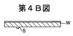
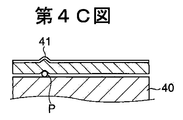
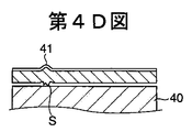
- the wafer is placed on a placement table (stage) 40 for exposure in the exposure machine. In this case, a part of the surface of the wafer W corresponding to the position of the particle P or the scratch S is raised (FIGS. 4C and 4D).
- Patent Document 1 a technique for preventing the back surface from being scratched by forming a protective film on the back surface of the wafer has been developed by the present applicant (see, for example, Patent Document 1).
- a protective film made of resin or the like is formed on the back surface of the wafer prior to a process that may cause damage to the back surface of the wafer, and after the photoresist film having a desired mask pattern is formed, the protective film is removed. .
- a technique has been developed to remove the scratches before the exposure of the photoresist when the back surface of the wafer is damaged without covering the back surface of the wafer with a protective film.
- a method of mechanically polishing the back surface of the wafer or a method of sputtering the back surface of the wafer with positive ions in plasma is known.
- the size of the scratch to be removed becomes small, and it is necessary to remove a small scratch, for example, a scratch having a size of several ⁇ m.
- a small scratch for example, a scratch having a size of several ⁇ m.
- the size of the grindstone is several hundred ⁇ m, it is not possible to appropriately remove only the scratch having a size of several ⁇ m.
- sputtering with positive ions has a large sputtering force, there is a problem that not only scratches but also the back surface of the wafer is scraped and the back surface becomes rough.
- An object of the present invention is to provide a substrate back surface flattening method capable of removing minute scratches without roughening the back surface of the substrate.
- a planarizing step of spraying a planarizing material containing at least a gas onto the back surface of a substrate, and an exposure step of exposing a photosensitive resin applied to the surface of the substrate are performed.
- a substrate backside planarization method is provided.
- the method further includes a detection step of detecting a position of a flaw or a foreign object on the back surface of the substrate prior to the flattening step.
- the flaw or the foreign object whose position is detected in the detection step is detected.
- the planarizing material is sprayed selectively.
- the planarizing material preferably includes a cluster of gas molecules formed by aggregating a large number of gas molecules contained in the gas.
- the gas molecule clusters are preferably ionized, the ionized gas molecule clusters are accelerated with a bias voltage, and the accelerated gas molecule clusters are neutralized. .
- the planarizing material is preferably an aerosol containing a large number of fine particles made of solid.
- the solid is preferably dry ice.
- a planarizing material containing at least gas is sprayed on the back surface of the substrate. Since the planarizing material contains gas, the kinetic energy of the planarizing material is not so large, and the physical impact force applied to the back surface of the substrate when the planarizing material collides with the back surface of the substrate is not so large. Therefore, minute scratches can be removed without roughening the back surface of the substrate.
- the position of a scratch or foreign object on the back surface of the substrate is detected prior to the flattening of the back surface of the substrate, and the planarizing material is selectively sprayed on the scratch or foreign object where the position has been detected. Therefore, it is not necessary to spray a planarizing material on the entire back surface of the substrate, and the back surface of the substrate can be efficiently planarized.
- the planarizing material is a cluster of gas molecules formed by aggregating a large number of gas molecules contained in the gas
- the physical impact force applied to a minute scratch at the time of collision is one gas. It is larger than the physical impact force that a molecule imparts to a minute scratch upon collision. Thereby, a minute crack can be destroyed and removed efficiently.
- a cluster of gas molecules collides with the back surface of the substrate, it is decomposed into a large number of gas molecules, and each gas molecule is scattered along the back surface of the substrate, so that each gas molecule is not driven into the back surface of the substrate.
- the cluster of gas molecules is ionized and the cluster of ionized gas molecules is accelerated by the bias voltage, the physical impact force imparted to the minute scratch at the time of collision with the back surface of the substrate is further increased.
- the back surface of the substrate can be planarized more efficiently.
- the accelerated cluster of gas molecules is neutralized, it is possible to prevent the substrate from being charged at the time of collision with the back surface of the substrate.
- the planarizing substance is an aerosol containing a large number of fine particles made of a solid
- the large number of fine particles can be made to collide with a minute scratch, and thus the minute scratch can be efficiently removed. it can.
- the solid is dry ice. Since dry ice is easily sublimated, it is possible to prevent dry ice as a solid from remaining as foreign matter on the back surface of the substrate after removal of minute scratches.
- FIG. 1 is a plan view schematically showing a configuration of a substrate processing system for executing a photoresist film forming process including a substrate back surface planarizing method according to an embodiment of the present invention.
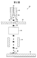
- FIG. 2 is a cross-sectional view schematically showing a configuration of a gas molecule cluster spraying section provided in the back surface planarization apparatus in FIG. [FIG. 3A] to [FIG. 3F]
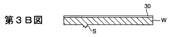
- FIG. 3A to FIG. 3F are process diagrams showing steps of a photoresist film forming process including a substrate back surface planarization method according to the present embodiment, which is executed by the substrate processing system of FIG. [FIG. 4A] to [FIG. 4F]
- FIGS. 4A to 4F are views for explaining the influence on the exposure processing of particles adhering to the back surface of the wafer and scratches generated.
- FIG. 1 is a plan view schematically showing a configuration of a substrate processing system that executes a photoresist film forming process including a substrate back surface planarizing method according to the present embodiment.
- a substrate processing system 10 includes a coater / developer 11, a back surface inspection device 12, a back surface flattening device 13, and an exposure machine 14, and includes a coater / developer 11, a back surface inspection device 12, and a back surface flattening device. 13 and the exposure unit 14 are arranged in series in this order, and a semiconductor wafer (hereinafter simply referred to as “wafer”) as a substrate to be processed is transported between the apparatuses.
- wafer semiconductor wafer
- the coater / developer 11 has a coater function for applying a photoresist, which is a positive photosensitive resin, to the wafer surface, and a photoresist subjected to an exposure process among photoresists cured by heating after application. It has the function of a developer that forms a photoresist film having a desired mask pattern by removing using an alkaline cleaning solution.
- the back surface inspection device 12 When the back surface inspection device 12 irradiates the back surface of the wafer with laser light, the back surface inspection device 12 receives the scattered light generated from the scratches generated on the back surface or particles as adhered foreign matter, thereby causing the scratches or attached particles generated on the back surface of the wafer. Detect the position and size.
- the exposure machine 14 includes a mounting table on which a wafer is mounted, and an ultraviolet irradiation lamp disposed to face the mounting table, and exposes the photoresist applied on the surface of the wafer by irradiating with ultraviolet rays.
- the photoresist is exposed to light.
- the photoresist is irradiated with ultraviolet rays only on the portion corresponding to the pattern inverted with respect to the desired mask pattern, the photoresist with the inverted pattern is altered and becomes alkali-soluble.
- the back surface flattening device 13 uses GCIB (Gas Cluster Ion Beam) to remove scratches and attached particles generated on the back surface of the wafer whose position and size are detected by the back surface inspection device 12.
- GCIB is a method in which gas is blown toward a vacuum atmosphere to form a cluster of gas molecules, the cluster is ionized, and the ionized cluster is accelerated by a bias voltage to collide with a wafer.
- FIG. 2 is a cross-sectional view schematically showing a configuration of a gas molecule cluster spraying portion provided in the back surface flattening apparatus in FIG.
- the gas molecule cluster spray unit 20 is arranged in a vacuum atmosphere in the back surface flattening device 13, and includes a cylindrical gas spray nozzle 21, an aperture plate 22, an ionizer 23, and a neutralization unit 24. Is provided.
- the cluster spray unit 20 is disposed so as to face the back surface of the wafer W accommodated in the back surface flattening device 13.
- the gas spray nozzles 21 are arranged in order, and a bias voltage is applied to at least a space between the ionizer 23 and the neutralizing unit 24.
- the gas spray nozzle 21 penetrates the gas spray nozzle 21 along the central axis direction, for example, a gas spray hole 25 having a diameter of 0.1 mm to 3.0 mm, and a wafer W side end portion in the gas spray nozzle 21. And a gas expansion hole 26 whose diameter increases in a funnel shape toward the end.
- the aperture plate 22 has an aperture 27 that opens in front of the gas spray hole 25 and penetrates the aperture plate 22 in the thickness direction.
- the gas spray nozzle 21 has a higher pressure than the vacuum atmosphere from the gas spray hole 25 toward the wafer W.
- the gas spray nozzle 21 has a pressure of 0.4 MPa to 0.9 MPa and a planarizing gas mainly composed of argon (Ar) gas. Spray (planarizing material).
- the atmosphere in the gas expansion hole 26 is almost vacuum in the cluster spraying portion 20 arranged in the vacuum atmosphere, the pressure of the planarizing gas sprayed from the gas spray hole 25 rapidly decreases, and the gas expansion hole The diameter of 26 also increases rapidly along the path of the gas molecules 28, and the volume of the planarizing gas increases rapidly. That is, the planarizing gas sprayed from the gas spray holes 25 undergoes a sudden adiabatic expansion, and each gas molecule 28 is rapidly cooled. When each gas molecule 28 that has moved independently one at a time is rapidly cooled, the kinetic energy is reduced and the gas molecules 28 are brought into close contact with each other by the intermolecular force (van der Waals force) acting between the gas molecules 28. Thereby, a cluster 29 composed of a large number of gas molecules 28 is formed.
- the cluster 29 that has passed through the aperture 27 enters the ionizer 23, and the ionizer 23 ionizes the cluster 29.
- the ionized cluster 29 is accelerated to a certain speed toward the wafer W by a bias voltage applied to the space between the ionizer 23 and the neutralization unit 24. Thereafter, when the accelerated cluster 29 passes through the neutralization part 24, the charge is removed and the cluster 29 is neutralized.
- the neutralized cluster 29 collides with the back surface of the wafer W while maintaining a constant speed, and physically destroys the scratch S by applying a physical impact force.
- the cluster 29 is an aggregate of a large number of gas molecules 28, the kinetic energy of the cluster 29 is larger than the kinetic energy of one gas molecule 28, and the physical impact force that the cluster 29 imparts to the scratch S at the time of collision is One gas molecule 28 is larger than the physical impact force applied to the scratch S at the time of collision.
- the cluster 29 can efficiently physically destroy and remove the scratches S, and can efficiently flatten the back surface of the wafer W.
- the cluster 29 is accelerated to a certain speed by the bias voltage, the physical impact force that the cluster 29 imparts to the scratch S at the time of collision can be increased, and the back surface of the wafer W can be more efficiently planarized. It can be carried out. Further, since the ionized cluster 29 is neutralized, it is possible to prevent the wafer W from being charged when it collides with the back surface of the wafer W.
- each gas molecule 28 is scattered along the back surface. Therefore, since each gas molecule 28 is not implanted into the back surface, the back surface is not roughened by the implantation of the gas molecules 28. Further, each gas molecule 28 scattered along the back surface selectively collides only with the scratch S protruding from the back surface. Thereby, it is possible to selectively remove only the scratches S (lateral sputtering effect).
- the cluster spray unit 20 can move in parallel to the back surface of the wafer W, and the amount of movement is larger than the diameter of the wafer W. Therefore, the cluster spray unit 20 can spray the cluster 29 toward the entire back surface of the wafer W. Note that the position of the wafer W in the back surface flattening apparatus 13 is fixed during the spraying of the clusters 29 by holding the periphery of the wafer W by a clamper (not shown).
- FIG. 3 is a process diagram showing a photoresist film forming process including the substrate back surface planarization method according to the present embodiment, which is executed by the substrate processing system of FIG.
- the coater / developer 11 wet-cleans the front and back surfaces of the wafer W (FIG. 3A), and applies a photoresist 30 to the front surface of the wafer W (FIG. 3B).
- the wafer W is carried into the back surface inspection apparatus 12, and the wafer W is turned upside down so that the back surface of the wafer W faces upward, and the laser light L is irradiated toward the back surface.
- the laser beam L is applied to the scratch S generated on the back surface, the laser beam L is reflected by the scratch S while being scattered to generate scattered light SL (FIG. 3C).
- the back surface inspection apparatus 12 detects the position and size of the scratch S by measuring the generation position, generation time, and intensity of the scattered light SL.
- the wafer W is carried into the back surface flattening device 13, and the clusters 29 are selectively sprayed toward the scratches S whose position and size are detected by the cluster spraying unit 20, and the scratches S are removed (FIG. 3D). Thereby, the back surface of the wafer W is planarized (FIG. 3E).
- the wafer W is turned upside down and carried into the exposure machine 14 and placed on the mounting table 31 of the exposure machine 14.
- the ultraviolet light UL is irradiated only to the portion corresponding to the pattern inverted with respect to the desired mask pattern toward the photoresist 30 applied to the surface of the wafer W (exposure processing).
- the photoresist 30 does not deviate from the focal point F of the ultraviolet light UL (FIG. 3F). In the photoresist 30, only the portion corresponding to the inverted pattern is obtained. Denatures and becomes alkali-soluble.
- the wafer W that has been subjected to the exposure process by the exposure machine 14 is carried into the coater / developer 11, and the coater / developer 11 uses an alkaline cleaning solution to cope with the inverted pattern in the photoresist 30 that has been altered to alkali solubility. Remove the parts to be used. As a result, a photoresist film having a desired mask pattern is formed on the surface of the wafer W.
- a cluster 29, which is an aggregate of a large number of gas molecules 28, is sprayed on the back surface of the wafer W before the photoresist 30 applied to the surface of the wafer W is exposed.
- the kinetic energy possessed by the cluster 29 is not as great as the kinetic energy possessed by the positive ions in the plasma drawn by the bias voltage, and the physical impact force applied to the back surface of the wafer W when the cluster 29 collides with the back surface of the wafer W is Not so big. Therefore, the minute scratches S can be removed without roughening the back surface of the wafer W.
- the cluster 29 efficiently and effectively applies the scratch S to the scratch S.
- the back surface of the wafer W can be flattened efficiently.
- the position and size of the scratch S on the back surface of the wafer W is detected prior to the flattening of the back surface of the wafer W by the back surface flattening device 13.
- the clusters 29 are selectively sprayed toward the detected scratch S. Therefore, it is not necessary to spray the cluster 29 on the entire back surface of the wafer W, and the back surface of the wafer W can be planarized more efficiently.
- the scratches S on the back surface of the wafer W are removed using the cluster 29.
- an aerosol containing fine dry ice particles as a large number of fine particles is applied to the wafer W. You may spray on the back. Since the size of the fine dry ice grains is also very small, it can collide with a minute scratch S having a size of about several ⁇ m generated on the back surface of the wafer W. Therefore, the scratch S can be efficiently removed by physically destroying the scratch S by applying a physical impact force.
- the kinetic energy of the fine dry ice grains is not as great as the kinetic energy of the cations in the plasma drawn by the bias voltage, even if the fine dry ice grains collide, the back surface of the wafer W is scraped and roughened. Absent. Further, since the dry ice is easily sublimated, it is possible to prevent the fine dry ice particles from remaining as foreign matter on the back surface of the wafer W after the fine scratches are removed.
- the cluster 29 exhibits a lateral sputtering effect, even if the cluster 29 is sprayed on the back surface of the wafer W for a long time, the gas molecules 28 are not implanted into the back surface of the wafer W, but the aerosol has a lateral sputtering effect. Therefore, if aerosol is sprayed onto the back surface of the wafer W for a long time, there is a possibility that fine dry ice grains are driven into the back surface of the wafer W. Therefore, it is preferable to adjust the spraying time of the aerosol based on the size of the detected scratch S.
- the back surface flattening device 13 is provided separately from the coater / developer 11 and the exposure machine 14, but the coater / developer 11 and the exposure machine 14 include the cluster spraying unit 20, and the photoresist 30 Prior to the exposure processing, the substrate W may be flattened on the back surface of the wafer W.
- the position and size of the scratch S on the back surface of the wafer W may be detected by another device before being processed in the substrate processing system 10.
- the position and size of the detected scratch S are stored in the memory of an external server, the memory of the controller of the substrate processing system 10 or the like, and the back surface flattening device 13 determines the wafer based on the stored position of the scratch S. It is preferable to spray the cluster 29 on the back surface of W.
- a planarizing gas mainly containing argon gas is used, but the planarizing gas is not limited to this.
- a planarizing gas that does not cause a chemical reaction with the film is used depending on the type of the film. Is preferred.
- the substrate to which the substrate back surface planarization method according to the above-described embodiment is applied is not limited to a semiconductor wafer, and various substrates used for FPD (Flat Panel Display) including LCD (Liquid Crystal Display), photomasks, and the like. CD substrate, printed circuit board, etc.
Landscapes
- Physics & Mathematics (AREA)
- General Physics & Mathematics (AREA)
- Engineering & Computer Science (AREA)
- Manufacturing & Machinery (AREA)
- Cleaning Or Drying Semiconductors (AREA)
- Exposure And Positioning Against Photoresist Photosensitive Materials (AREA)
- Exposure Of Semiconductors, Excluding Electron Or Ion Beam Exposure (AREA)
- Drying Of Semiconductors (AREA)
Abstract
基板の裏面を荒らすことなく微小な傷を除去することができる基板裏面平坦化方法を提供する。ウエハWの裏面における傷Sの位置や大きさが検出され、位置や大きさが検出された傷Sへ選択的に多数のガス分子28が集合して形成されたガス分子28のクラスター29が吹き付けられ、ウエハWの表面に塗布されたフォトレジスト30が露光される。
Description
本発明は、基板裏面平坦化方法に関し、特に、露光・現像によって表面に所望のマスクパターンのフォトレジスト膜が形成される基板の基板裏面平坦化方法に関する。
基板としてのウエハの表面にプラズマを利用して所望のパターンの配線溝やビアホールを形成する基板処理システムは、ポジ型のフォトレジストをウエハの表面に塗布するコータと、加熱等によって硬化したフォトレジストの一部を露光する露光機と、ウエハの表面から露光されたフォトレジストを現像液によって除去してフォトレジスト膜を形成するデベロッパと、ウエハの表面にエッチング処理、例えば、RIE(Reactive Ion Etching)処理を施すエッチング装置と、フォトレジスト膜を除去する洗浄装置とを備える。
露光機では所望のマスクパターンに対して反転したパターンの紫外線光をウエハの表面におけるフォトレジストに照射するが、近年、所望のマスクパターンの微細化に伴い短波長、例えば、波長が数10nmの紫外線光が露光機で用いられる。波長が短いと許容焦点深度も小さくなり、露光時に許容されるウエハの平面度、傾きも小さくなる。
ところで、ウエハが基板処理システムにおいて搬送される際、浮遊しているパーティクルがウエハの裏面に付着したり、ウエハが他の部材と接触することによってウエハの裏面に傷が生じることがある。例えば、図4Aや図4Bに示すように、ウエハWの裏面にパーティクルPが付着し、若しくは傷Sが生じていると、露光機において露光のためにウエハを載置台(ステージ)40に載置した際、パーティクルPや傷Sの位置に対応するウエハWの表面の一部が盛り上がる(図4C、図4D)。盛り上がったウエハWの表面の一部におけるフォトレジスト膜の一部41は、紫外線光ULの焦点Fからずれてしまうため(図4E、図4F)、結果として、所望のマスクパターンのフォトレジスト膜を形成するのが困難になる。
そこで、ウエハの裏面に保護膜を形成することによって裏面において傷が生じるのを防止する技術が本出願人によって開発されている(例えば、特許文献1参照。)。この技術では、ウエハの裏面に傷が生じる可能性のある工程に先立ってウエハの裏面に樹脂等からなる保護膜を形成し、所望のマスクパターンのフォトレジスト膜を形成した後に保護膜を除去する。しかしながら、上記技術では保護膜の除去に時間を要し、また、保護膜が他の部材と接触する際、保護膜の一部が剥がれてパーティクルとなるおそれがある。
これに対応して、近年、ウエハの裏面を保護膜で覆うことなく、ウエハの裏面に傷が生じた場合、フォトレジストの露光前に当該傷を除去する技術が開発されている。このような技術としては、例えば、ウエハの裏面を機械的に研磨する方法やウエハの裏面をプラズマ中の陽イオンによってスパッタする方法が知られている。
しかしながら、近年の所望のマスクパターンの微細化に伴う許容焦点深度の縮小化により、除去すべき傷の大きさは小さくなり、微小な傷、例えば、大きさが数μmの傷を除去する必要があるが、上述した機械的研磨では砥石の目の大きさが数100μmであるため、大きさが数μmの傷のみを適切に除去することができない。また、陽イオンによるスパッタではスパッタ力が大きいため、傷だけでなくウエハの裏面も削り、裏面が荒れるという問題がある。
本発明の目的は、基板の裏面を荒らすことなく微小な傷を除去することができる基板裏面平坦化方法を提供することにある。
上記目的を達成するために、本発明によれば、基板の裏面へ少なくともガスを含む平坦化物質を吹き付ける平坦化ステップと、前記基板の表面に塗布された感光性樹脂を露光する露光ステップとを有する基板裏面平坦化方法が提供される。
本発明において、前記平坦化ステップに先立って前記基板の裏面における傷又は異物の位置を検出する検出ステップをさらに有し、前記平坦化ステップでは、前記検出ステップにおいて位置が検出された傷又は異物へ選択的に前記平坦化物質を吹き付けることが好ましい。
本発明において、前記平坦化物質は前記ガスに含まれる多数のガス分子が集合して形成されたガス分子のクラスターを含むことが好ましい。
本発明において、前記平坦化ステップにおいて、前記ガス分子のクラスターをイオン化し、該イオン化されたガス分子のクラスターをバイアス電圧で加速し、該加速されたガス分子のクラスターを中性化することが好ましい。
本発明において、前記平坦化物質は固体からなる多数の微粒子を含むエアロゾルであることが好ましい。
本発明において、前記固体はドライアイスであることが好ましい。
本発明によれば、基板の表面に塗布された感光性樹脂が露光される前に、基板の裏面へ少なくともガスを含む平坦化物質が吹き付けられる。平坦化物質はガスを含むので、当該平坦化物質が有する運動エネルギーはさほど大きくなく、平坦化物質が基板の裏面に衝突した際に該基板の裏面へ付与する物理的衝撃力はさほど大きくない。したがって、基板の裏面を荒らすことなく微小な傷を除去することができる。
本発明によれば、基板の裏面の平坦化に先立って基板の裏面における傷又は異物の位置が検出され、該位置が検出された傷又は異物へ選択的に平坦化物質が吹き付けられる。したがって、基板の裏面の全面に平坦化物質を吹き付ける必要がなく、基板の裏面の平坦化を効率良く行うことができる。
本発明によれば、平坦化物質はガスに含まれる多数のガス分子が集合して形成されたガス分子のクラスターであるので、衝突時に微小な傷へ付与する物理的衝撃力は、1つのガス分子が衝突時に微小な傷へ付与する物理的衝撃力よりも大きい。これにより、微小な傷を効率良く破壊して除去することができる。また、ガス分子のクラスターは基板の裏面へ衝突した際、多数のガス分子へ分解し、各ガス分子は基板の裏面に沿って飛散するので、各ガス分子が基板の裏面へ打ち込まれることが無く、もって、基板の裏面が荒れるのを確実に防止することができる。
本発明によれば、ガス分子のクラスターがイオン化され、該イオン化されたガス分子のクラスターがバイアス電圧で加速されるので、基板の裏面への衝突時に微小な傷へ付与する物理的衝撃力をより大きくすることができ、もって、基板の裏面の平坦化をより効率良く行うことができる。また、加速されたガス分子のクラスターが中性化されるので、基板の裏面への衝突時に基板が帯電するのを防止することができる。
本発明によれば、平坦化物質は固体からなる多数の微粒子を含むエアロゾルであるので、多数の微粒子を微小な傷にも衝突させることができ、もって、微小な傷を効率良く除去することができる。
本発明によれば、固体はドライアイスである。ドライアイスは昇華しやすいので、微小な傷の除去後、固体としてのドライアイスが基板の裏面に異物として残留するのを防止することができる。
[図1]本発明の実施の形態に係る基板裏面平坦化方法を含むフォトレジスト膜形成処理を実行する基板処理システムの構成を概略的に示す平面図である。
[図2]図1における裏面平坦化装置が備えるガス分子のクラスター吹き付け部の構成を概略的に示す断面図である。
[図3A]~[図3F]図1の基板処理システムが実行する、本実施の形態に係る基板裏面平坦化方法を含むフォトレジスト膜形成処理の各工程を示す工程図である。
[図4A]~[図4F]ウエハの裏面に付着したパーティクルや生じた傷の露光処理への影響を説明するための図である。
[図2]図1における裏面平坦化装置が備えるガス分子のクラスター吹き付け部の構成を概略的に示す断面図である。
[図3A]~[図3F]図1の基板処理システムが実行する、本実施の形態に係る基板裏面平坦化方法を含むフォトレジスト膜形成処理の各工程を示す工程図である。
[図4A]~[図4F]ウエハの裏面に付着したパーティクルや生じた傷の露光処理への影響を説明するための図である。
以下、本発明の実施の形態について図面を参照しながら詳細に説明する。
図1は、本実施の形態に係る基板裏面平坦化方法を含むフォトレジスト膜形成処理を実行する基板処理システムの構成を概略的に示す平面図である。
図1において、基板処理システム10は、コータ/デベロッパ11と、裏面検査装置12と、裏面平坦化装置13と、露光機14とを備え、コータ/デベロッパ11、裏面検査装置12、裏面平坦化装置13及び露光機14はこの順で直列配置され、被処理基板としての半導体ウエハ(以下、単に「ウエハ」という。)が各装置間で搬送される。
コータ/デベロッパ11は、ウエハの表面にポジ型の感光性樹脂であるフォトレジストを塗布するコータの機能と、塗布後に加熱等によって硬化されたフォトレジストのうち、露光処理が施されたフォトレジストをアルカリ性の洗浄液を用いて除去することによって所望のマスクパターンのフォトレジスト膜を形成するデベロッパの機能とを有する。
裏面検査装置12は、ウエハの裏面にレーザ光を照射した際、裏面に生じた傷や付着した異物としてのパーティクルから生じる散乱光を受光することにより、ウエハの裏面に生じた傷や付着したパーティクルの位置及び大きさを検出する。
露光機14は、ウエハが載置される載置台と、該載置台に対向して配置される紫外線照射ランプとを備え、ウエハの表面に塗布されたフォトレジストに紫外線を照射して露光することにより、フォトレジストに露光処理を施す。ここで、フォトレジストには所望のマスクパターンに対して反転したパターンに対応する部分にのみ紫外線が照射されるので、反転したパターンのフォトレジストが変質してアルカリ可溶性になる。
裏面平坦化装置13は、GCIB(Gas Cluster Ion Beam)を用いて裏面検査装置12によって位置及び大きさが検出されたウエハの裏面に生じた傷や付着したパーティクルを除去する。GCIBとは、真空雰囲気に向けてガスを吹き付けてガス分子のクラスターを形成し、さらに該クラスターをイオン化し、バイアス電圧によってイオン化されたクラスターを加速してウエハに衝突させる方法である。
図2は、図1における裏面平坦化装置が備えるガス分子のクラスター吹き付け部の構成を概略的に示す断面図である。
図2において、ガス分子のクラスター吹き付け部20は、裏面平坦化装置13における真空雰囲気中に配され、筒状のガス噴霧ノズル21と、アパーチャー板22と、イオナイザー23と、中性化部24とを備える。クラスター吹き付け部20は裏面平坦化装置13に収容されたウエハWの裏面に対向するように配され、該クラスター吹き付け部20では、ウエハW側から中性化部24、イオナイザー23、アパーチャー板22及びガス噴霧ノズル21が順に配され、少なくともイオナイザー23及び中性化部24の間の空間にバイアス電圧が印加される。
ガス噴霧ノズル21は、該ガス噴霧ノズル21を中心軸方向に沿って貫通する、例えば、直径が0.1mm~3.0mmであるガス噴霧穴25と、ガス噴霧ノズル21におけるウエハW側端部に穿孔されて該端部に向けて漏斗状に直径が大きくなるガス膨張穴26とを有する。アパーチャー板22は、ガス噴霧穴25に正対して開口し、且つ該アパーチャー板22を厚さ方向に貫通するアパーチャー27を有する。
ガス噴霧ノズル21はウエハWに向けてガス噴霧穴25から真空雰囲気よりも高圧で、例えば、圧力が0.4MPa乃至0.9MPaのいずれかでアルゴン(Ar)ガスを主成分とする平坦化ガス(平坦化物質)を噴霧する。
真空雰囲気中に配されたクラスター吹き付け部20ではガス膨張穴26内の雰囲気もほぼ真空となるため、ガス噴霧穴25から噴霧された平坦化ガスの圧力が急激に低下するとともに、該ガス膨張穴26の直径もガス分子28の進路に沿って急激に大きくなり、平坦化ガスの体積が急激に大きくなる。すなわち、ガス噴霧穴25から噴霧された平坦化ガスは急激な断熱膨張を起こして各ガス分子28が急冷される。当初1つ1つ独立して移動していた各ガス分子28は急冷されると、運動エネルギーが低下して各ガス分子28間に作用する分子間力(ファンデルワールス力)によって互いに密着し、これにより、多数のガス分子28からなるクラスター29が形成される。
アパーチャー板22ではアパーチャー27がガス噴霧穴25に正対するので、形成された多数のクラスター29のうち、ガス噴霧穴25からアパーチャー27に向けて進行するクラスター29のみがアパーチャー27を通過する。その結果、クラスター29の進行方向が一様に定められる。
アパーチャー27を通過したクラスター29はイオナイザー23へ進入し、該イオナイザー23はクラスター29をイオン化する。イオン化されたクラスター29は、イオナイザー23及び中性化部24の間の空間に印加されたバイアス電圧によってウエハWに向けて一定の速度まで加速される。その後、加速されたクラスター29は中性化部24を通過する際に電荷が除去されて中性化される。中性化されたクラスター29は一定の速度を維持したまま、ウエハWの裏面に衝突して傷Sに物理的衝撃力を与えて物理的に破壊する。特に、クラスター29は多数のガス分子28の集合体であるため、クラスター29の運動エネルギーは1つのガス分子28の運動エネルギーよりも大きく、クラスター29が衝突時に傷Sへ付与する物理的衝撃力は、1つのガス分子28が衝突時に傷Sへ付与する物理的衝撃力よりも大きい。
これにより、クラスター29は傷Sを効率良く物理的に破壊して除去し、ウエハWの裏面の平坦化を効率良く行うことができる。
また、クラスター29はバイアス電圧によって一定の速度まで加速されるので、クラスター29が衝突時に傷Sへ付与する物理的衝撃力をより大きくすることができ、ウエハWの裏面の平坦化をより効率良く行うことができる。また、イオン化されたクラスター29が中性化されるので、ウエハWの裏面への衝突時にウエハWが帯電するのを防止することができる。
一方、クラスター29は一般にウエハWの裏面等に衝突した際、多数のガス分子28へ分解し、各ガス分子28は裏面に沿って飛散する。したがって、各ガス分子28は裏面に打ち込まれることが無いため、ガス分子28の打ち込みによって裏面が荒れることがない。さらに、裏面に沿って飛散する各ガス分子28は裏面から突出する傷Sにのみ選択的に衝突する。これにより、選択的に傷Sのみを除去することができる(ラテラルスパッタ効果)。
裏面平坦化装置13では、クラスター吹き付け部20がウエハWの裏面に対して平行に移動することでき、その移動量はウエハWの直径よりも大きい。したがって、クラスター吹き付け部20はウエハWの裏面全体に向けてクラスター29を吹き付けることができる。なお、裏面平坦化装置13においてウエハWは、その周縁部をクランパー(図示しない)によって保持されることにより、クラスター29の吹きつけの間、位置が固定される。
図3は、図1の基板処理システムが実行する、本実施の形態に係る基板裏面平坦化方法を含むフォトレジスト膜形成処理を示す工程図である。
まず、コータ/デベロッパ11においてウエハWの表面や裏面をウェット洗浄し(図3A)、ウエハWの表面にフォトレジスト30を塗布する(図3B)。
次いで、ウエハWを裏面検査装置12へ搬入し、ウエハWの上下を反転させてウエハWの裏面を上向きにし、該裏面に向けてレーザ光Lを照射する。レーザ光Lが裏面において生じた傷Sに照射された場合、傷Sによってレーザ光Lは散乱しながら反射して散乱光SLを生じさせる(図3C)。裏面検査装置12は散乱光SLの発生位置や発生時間、強度を計測することによって傷Sの位置や大きさを検出する。
次いで、ウエハWを裏面平坦化装置13へ搬入し、クラスター吹き付け部20によって位置や大きさが検出された傷Sに向けて選択的にクラスター29を吹き付け、傷Sを除去する(図3D)。これにより、ウエハWの裏面は平坦化される(図3E)。
次いで、ウエハWの上下を反転させて露光機14へ搬入し、露光機14の載置台31に載置する。ここで、ウエハWの裏面は平坦化されているので、ウエハWの表面の一部が盛り上がることがない。その後、ウエハWの表面に塗布されたフォトレジスト30に向けて所望のマスクパターンに対して反転したパターンに対応する部分にのみ紫外線光ULを照射する(露光処理)。このとき、ウエハWの表面の一部が盛り上がることがないため、フォトレジスト30が紫外線光ULの焦点Fからずれることがなく(図3F)、フォトレジスト30では、反転したパターンに対応する部分のみが変質してアルカリ可溶性になる。
次いで、露光機14にて露光処理が施されたウエハWをコータ/デベロッパ11へ搬入し、コータ/デベロッパ11はアルカリ性の洗浄液を用いて、アルカリ可溶性に変質したフォトレジスト30における反転したパターンに対応する部分を除去する。その結果、ウエハWの表面において所望のマスクパターンのフォトレジスト膜が形成される。
図3のフォトレジスト膜形成処理によれば、ウエハWの表面に塗布されたフォトレジスト30が露光される前に、ウエハWの裏面へ多数のガス分子28の集合体であるクラスター29が吹き付けられる。クラスター29が有する運動エネルギーはバイアス電圧によって引き込まれるプラズマ中の陽イオンが有する運動エネルギーほど大きくなく、クラスター29がウエハWの裏面に衝突した際に該ウエハWの裏面へ付与する物理的衝撃力はさほど大きくない。したがって、ウエハWの裏面を荒らすことなく微小な傷Sを除去することができる。
また、クラスター29が衝突時に傷Sへ付与する物理的衝撃力は、1つのガス分子28が衝突時に傷Sへ付与する物理的衝撃力よりも大きいので、クラスター29は傷Sを効率良く物理的に破壊して除去し、ウエハWの裏面の平坦化を効率良く行うことができる。
上述した図3のフォトレジスト膜形成処理では、裏面平坦化装置13によるウエハWの裏面の平坦化に先立ってウエハWの裏面における傷Sの位置や大きさが検出され、該位置や大きさが検出された傷Sに向けて選択的にクラスター29が吹き付けられる。したがって、ウエハWの裏面の全面にクラスター29を吹き付ける必要がなく、ウエハWの裏面の平坦化をより効率良く行うことができる。
上述した図3のフォトレジスト膜形成処理では、クラスター29を用いてウエハWの裏面における傷Sを除去したが、クラスター29の代わりに多数の微粒子としての微小ドライアイス粒を含むエアロゾルをウエハWの裏面へ吹き付けてもよい。微小ドライアイス粒の大きさも非常に小さいため、ウエハWの裏面に生じた大きさが数μm程度の微小な傷Sにも衝突可能である。したがって、傷Sに物理的衝撃力を与えて物理的に破壊することによって傷Sを効率良く除去することができる。また、微小ドライアイス粒が有する運動エネルギーはバイアス電圧によって引き込まれるプラズマ中の陽イオンが有する運動エネルギーほど大きくないため、微小ドライアイス粒が衝突してもウエハWの裏面が削れられて荒れることはない。さらに、ドライアイスは昇華しやすいので、微小な傷の除去後、微小ドライアイス粒がウエハWの裏面に異物として残留するのを防止することができる。
ところで、クラスター29はラテラルスパッタ効果を奏するので、長時間に亘ってクラスター29をウエハWの裏面に吹き付けても、ガス分子28がウエハWの裏面に打ち込まれることはないが、エアロゾルはラテラルスパッタ効果を奏することができないので、長時間に亘ってエアロゾルをウエハWの裏面に吹き付けると、微小ドライアイス粒がウエハWの裏面に打ち込まれる可能性がある。したがって、検出された傷Sの大きさに基づいて、エアロゾルの吹き付け時間を調整するのが好ましい。
上述した図3のフォトレジスト膜形成処理では、ウエハWの裏面に生じた微小な傷Sが除去されたが、ウエハWの裏面に付着した異物としてのパーティクルもクラスター29やエアロゾルを吹き付けることによって除去することができる。
上述した基板処理システム10では、コータ/デベロッパ11や露光機14とは別に裏面平坦化装置13が設けられたが、コータ/デベロッパ11や露光機14がクラスター吹き付け部20を備え、フォトレジスト30の露光処理に先立ってウエハWの基板裏面平坦化を行ってもよい。
また、上述した基板処理システム10は裏面検査装置12を備えるが、基板処理システム10において処理される前に他の装置によってウエハWの裏面における傷Sの位置や大きさを検出してもよい。この場合、検出された傷Sの位置や大きさは外部サーバのメモリや基板処理システム10のコントローラのメモリ等に格納され、裏面平坦化装置13は該格納された傷Sの位置に基づいてウエハWの裏面にクラスター29を吹き付けるのが好ましい。
さらに、基板処理システム10ではアルゴンガスを主成分とする平坦化ガスが用いられたが、平坦化ガスはこれに限られない。例えば、ウエハWの裏面に二酸化硅素(SiO2)膜、窒化硅素(SiN)膜又は金属膜が形成されている場合、膜の種類に応じて該膜と化学反応を起こさない平坦化ガスを用いるのが好ましい。
また、上述した実施の形態に係る基板裏面平坦化方法が適用される基板は半導体ウエハに限られず、LCD(Liquid Crystal Display)等を含むFPD(Flat Panel Display)等に用いる各種基板や、フォトマスク、CD基板、プリント基板等であってもよい。
F 焦点
S 傷
UL 紫外線光
W ウエハ
10 基板処理システム
12 裏面検査装置
13 裏面平坦化装置
20 クラスター吹き付け部
30 フォトレジスト
S 傷
UL 紫外線光
W ウエハ
10 基板処理システム
12 裏面検査装置
13 裏面平坦化装置
20 クラスター吹き付け部
30 フォトレジスト
Claims (6)
- 基板の裏面へ少なくともガスを含む平坦化物質を吹き付ける平坦化ステップと、
前記基板の表面に塗布された感光性樹脂を露光する露光ステップとを有することを特徴とする基板裏面平坦化方法。 - 前記平坦化ステップに先立って前記基板の裏面における傷又は異物の位置を検出する検出ステップをさらに有し、
前記平坦化ステップでは、前記検出ステップにおいて位置が検出された傷又は異物へ選択的に前記平坦化物質を吹き付けることを特徴とする請求項1記載の基板裏面平坦化方法。 - 前記平坦化物質は前記ガスに含まれる多数のガス分子が集合して形成されたガス分子のクラスターを含むことを特徴とする請求項1記載の基板裏面平坦化方法。
- 前記平坦化ステップにおいて、前記ガス分子のクラスターをイオン化し、該イオン化されたガス分子のクラスターをバイアス電圧で加速し、該加速されたガス分子のクラスターを中性化することを特徴とする請求項3記載の基板裏面平坦化方法。
- 前記平坦化物質は固体からなる多数の微粒子を含むエアロゾルであることを特徴とする請求項1記載の基板裏面平坦化方法。
- 前記固体はドライアイスであることを特徴とする請求項5記載の基板裏面平坦化方法。
Applications Claiming Priority (2)
| Application Number | Priority Date | Filing Date | Title |
|---|---|---|---|
| JP2010-033483 | 2010-02-18 | ||
| JP2010033483A JP2011171487A (ja) | 2010-02-18 | 2010-02-18 | 基板裏面平坦化方法 |
Publications (1)
| Publication Number | Publication Date |
|---|---|
| WO2011102278A1 true WO2011102278A1 (ja) | 2011-08-25 |
Family
ID=44482865
Family Applications (1)
| Application Number | Title | Priority Date | Filing Date |
|---|---|---|---|
| PCT/JP2011/052796 Ceased WO2011102278A1 (ja) | 2010-02-18 | 2011-02-03 | 基板裏面平坦化方法 |
Country Status (3)
| Country | Link |
|---|---|
| JP (1) | JP2011171487A (ja) |
| TW (1) | TW201201249A (ja) |
| WO (1) | WO2011102278A1 (ja) |
Families Citing this family (4)
| Publication number | Priority date | Publication date | Assignee | Title |
|---|---|---|---|---|
| JP5984424B2 (ja) * | 2012-02-27 | 2016-09-06 | 国立大学法人京都大学 | 基板洗浄方法、基板洗浄装置及び真空処理装置 |
| US10147613B2 (en) * | 2014-06-30 | 2018-12-04 | Tokyo Electron Limited | Neutral beam etching of Cu-containing layers in an organic compound gas environment |
| CN106449501B (zh) * | 2015-08-04 | 2019-12-31 | 北大方正集团有限公司 | 改善外延片背面平整度的方法和外延片 |
| WO2019077877A1 (ja) * | 2017-10-17 | 2019-04-25 | 富士電機株式会社 | 炭化珪素半導体装置および炭化珪素半導体装置の製造方法 |
Citations (5)
| Publication number | Priority date | Publication date | Assignee | Title |
|---|---|---|---|---|
| JPS6226814A (ja) * | 1985-07-26 | 1987-02-04 | Toshiba Corp | 露光装置 |
| JPH06176995A (ja) * | 1992-12-03 | 1994-06-24 | Nikon Corp | 基板搬送装置 |
| JP2005093312A (ja) * | 2003-09-19 | 2005-04-07 | Ulvac Japan Ltd | ガスクラスターイオンビーム装置 |
| JP2005179752A (ja) * | 2003-12-19 | 2005-07-07 | Ulvac Japan Ltd | ガスクラスターイオンビーム装置 |
| WO2008121628A1 (en) * | 2007-03-30 | 2008-10-09 | Tel Epion Inc. | Apparatus and methods for systematic non-uniformity correction using a gas cluster ion beam |
Family Cites Families (5)
| Publication number | Priority date | Publication date | Assignee | Title |
|---|---|---|---|---|
| JPH0653199A (ja) * | 1992-06-03 | 1994-02-25 | Teisan Kk | ドライアイススティックを使った表面洗浄方法 |
| JPH11265877A (ja) * | 1998-03-16 | 1999-09-28 | Toshiba Corp | ウエハの平坦化方法及び平坦化装置 |
| JP3915261B2 (ja) * | 1998-07-29 | 2007-05-16 | Tdk株式会社 | マイクロデバイスの研磨方法 |
| JP4508779B2 (ja) * | 2004-08-23 | 2010-07-21 | Hoya株式会社 | マスクブランク用基板の製造方法、マスクブランクの製造方法、及び露光用マスクの製造方法 |
| JP5227688B2 (ja) * | 2008-07-28 | 2013-07-03 | 株式会社堀場製作所 | マスク用基板検査装置 |
-
2010
- 2010-02-18 JP JP2010033483A patent/JP2011171487A/ja not_active Ceased
-
2011
- 2011-02-03 WO PCT/JP2011/052796 patent/WO2011102278A1/ja not_active Ceased
- 2011-02-17 TW TW100105177A patent/TW201201249A/zh unknown
Patent Citations (5)
| Publication number | Priority date | Publication date | Assignee | Title |
|---|---|---|---|---|
| JPS6226814A (ja) * | 1985-07-26 | 1987-02-04 | Toshiba Corp | 露光装置 |
| JPH06176995A (ja) * | 1992-12-03 | 1994-06-24 | Nikon Corp | 基板搬送装置 |
| JP2005093312A (ja) * | 2003-09-19 | 2005-04-07 | Ulvac Japan Ltd | ガスクラスターイオンビーム装置 |
| JP2005179752A (ja) * | 2003-12-19 | 2005-07-07 | Ulvac Japan Ltd | ガスクラスターイオンビーム装置 |
| WO2008121628A1 (en) * | 2007-03-30 | 2008-10-09 | Tel Epion Inc. | Apparatus and methods for systematic non-uniformity correction using a gas cluster ion beam |
Also Published As
| Publication number | Publication date |
|---|---|
| TW201201249A (en) | 2012-01-01 |
| JP2011171487A (ja) | 2011-09-01 |
Similar Documents
| Publication | Publication Date | Title |
|---|---|---|
| KR102345187B1 (ko) | 웨이퍼의 가공 방법 | |
| US8206510B2 (en) | Method and apparatus for an in-situ ultraviolet cleaning tool | |
| JP5235506B2 (ja) | パターン転写装置及びデバイス製造方法 | |
| US9209010B2 (en) | Substrate cleaning method and substrate cleaning device | |
| US8728711B2 (en) | Cleaning reticle, method for cleaning reticle stage, and method for manufacturing semiconductor device | |
| US20120279519A1 (en) | Integrated Substrate Cleaning System and Method | |
| US20080002164A1 (en) | Apparatus and method for immersion lithography | |
| US6864458B2 (en) | Iced film substrate cleaning | |
| KR20030080182A (ko) | 리소그래피장치, 장치세정방법, 디바이스제조방법 및 그제조된 디바이스 | |
| US8419963B2 (en) | Polishing method | |
| JP2010199239A (ja) | 被処理基板の除電方法及び基板処理装置 | |
| TWI661925B (zh) | 壓印裝置、壓印方法及物品的製造方法 | |
| KR20170034316A (ko) | 웨이퍼의 가공 방법 | |
| CN101042988B (zh) | 基板处理方法 | |
| WO2011102278A1 (ja) | 基板裏面平坦化方法 | |
| KR20200067092A (ko) | 용기, 처리 장치, 파티클 제거 방법, 및 물품 제조 방법 | |
| JP2008226991A (ja) | プラズマ処理装置 | |
| WO2020009787A1 (en) | Photomask pellicle glue residue removal | |
| KR20230152583A (ko) | 이물 제거 방법, 형성 방법, 물품 제조 방법, 이물 제거 장치, 및 시스템 | |
| KR20230152572A (ko) | 이물 제거 방법, 형성 방법, 물품 제조 방법, 이물 제거 장치, 시스템, 및 템플릿 | |
| CN117891138A (zh) | 抛光方法及抛光系统 | |
| JP2023072644A (ja) | 異物除去方法、異物除去装置、及び物品の製造方法 | |
| KR20080095420A (ko) | 레이저 충격파가 인가된 화학액을 이용한 기판 세정 장치및 방법 | |
| JP2009070982A (ja) | 飛散粒子除去装置、飛散粒子の低減方法、光源装置、照明光学装置、露光装置及び電子デバイスの製造方法 | |
| JP2003282400A (ja) | レーザ薄膜除去装置 |
Legal Events
| Date | Code | Title | Description |
|---|---|---|---|
| 121 | Ep: the epo has been informed by wipo that ep was designated in this application |
Ref document number: 11744565 Country of ref document: EP Kind code of ref document: A1 |
|
| NENP | Non-entry into the national phase |
Ref country code: DE |
|
| 122 | Ep: pct application non-entry in european phase |
Ref document number: 11744565 Country of ref document: EP Kind code of ref document: A1 |