WO2011081129A1 - プリント基板の製造方法及びこれを用いたプローブ基板の製造方法 - Google Patents
プリント基板の製造方法及びこれを用いたプローブ基板の製造方法 Download PDFInfo
- Publication number
- WO2011081129A1 WO2011081129A1 PCT/JP2010/073529 JP2010073529W WO2011081129A1 WO 2011081129 A1 WO2011081129 A1 WO 2011081129A1 JP 2010073529 W JP2010073529 W JP 2010073529W WO 2011081129 A1 WO2011081129 A1 WO 2011081129A1
- Authority
- WO
- WIPO (PCT)
- Prior art keywords
- manufacturing
- transmission line
- substrate
- printed circuit
- probe
- Prior art date
- Legal status (The legal status is an assumption and is not a legal conclusion. Google has not performed a legal analysis and makes no representation as to the accuracy of the status listed.)
- Ceased
Links
Images












Classifications
-
- H—ELECTRICITY
- H05—ELECTRIC TECHNIQUES NOT OTHERWISE PROVIDED FOR
- H05K—PRINTED CIRCUITS; CASINGS OR CONSTRUCTIONAL DETAILS OF ELECTRIC APPARATUS; MANUFACTURE OF ASSEMBLAGES OF ELECTRICAL COMPONENTS
- H05K3/00—Apparatus or processes for manufacturing printed circuits
- H05K3/40—Forming printed elements for providing electric connections to or between printed circuits
- H05K3/403—Edge contacts; Windows or holes in the substrate having plural connections on the walls thereof
-
- G—PHYSICS
- G01—MEASURING; TESTING
- G01R—MEASURING ELECTRIC VARIABLES; MEASURING MAGNETIC VARIABLES
- G01R3/00—Apparatus or processes specially adapted for the manufacture or maintenance of measuring instruments, e.g. of probe tips
-
- G—PHYSICS
- G01—MEASURING; TESTING
- G01R—MEASURING ELECTRIC VARIABLES; MEASURING MAGNETIC VARIABLES
- G01R1/00—Details of instruments or arrangements of the types included in groups G01R5/00 - G01R13/00 and G01R31/00
- G01R1/02—General constructional details
- G01R1/06—Measuring leads; Measuring probes
- G01R1/067—Measuring probes
- G01R1/06772—High frequency probes
-
- H—ELECTRICITY
- H05—ELECTRIC TECHNIQUES NOT OTHERWISE PROVIDED FOR
- H05K—PRINTED CIRCUITS; CASINGS OR CONSTRUCTIONAL DETAILS OF ELECTRIC APPARATUS; MANUFACTURE OF ASSEMBLAGES OF ELECTRICAL COMPONENTS
- H05K2201/00—Indexing scheme relating to printed circuits covered by H05K1/00
- H05K2201/01—Dielectrics
- H05K2201/0104—Properties and characteristics in general
- H05K2201/0129—Thermoplastic polymer, e.g. auto-adhesive layer; Shaping of thermoplastic polymer
-
- H—ELECTRICITY
- H05—ELECTRIC TECHNIQUES NOT OTHERWISE PROVIDED FOR
- H05K—PRINTED CIRCUITS; CASINGS OR CONSTRUCTIONAL DETAILS OF ELECTRIC APPARATUS; MANUFACTURE OF ASSEMBLAGES OF ELECTRICAL COMPONENTS
- H05K2203/00—Indexing scheme relating to apparatus or processes for manufacturing printed circuits covered by H05K3/00
- H05K2203/01—Tools for processing; Objects used during processing
- H05K2203/0147—Carriers and holders
- H05K2203/0152—Temporary metallic carrier, e.g. for transferring material
-
- H—ELECTRICITY
- H05—ELECTRIC TECHNIQUES NOT OTHERWISE PROVIDED FOR
- H05K—PRINTED CIRCUITS; CASINGS OR CONSTRUCTIONAL DETAILS OF ELECTRIC APPARATUS; MANUFACTURE OF ASSEMBLAGES OF ELECTRICAL COMPONENTS
- H05K2203/00—Indexing scheme relating to apparatus or processes for manufacturing printed circuits covered by H05K3/00
- H05K2203/02—Details related to mechanical or acoustic processing, e.g. drilling, punching, cutting, using ultrasound
- H05K2203/0242—Cutting around hole, e.g. for disconnecting land or Plated Through-Hole [PTH] or for partly removing a PTH
-
- H—ELECTRICITY
- H05—ELECTRIC TECHNIQUES NOT OTHERWISE PROVIDED FOR
- H05K—PRINTED CIRCUITS; CASINGS OR CONSTRUCTIONAL DETAILS OF ELECTRIC APPARATUS; MANUFACTURE OF ASSEMBLAGES OF ELECTRICAL COMPONENTS
- H05K2203/00—Indexing scheme relating to apparatus or processes for manufacturing printed circuits covered by H05K3/00
- H05K2203/06—Lamination
- H05K2203/063—Lamination of preperforated insulating layer
-
- H—ELECTRICITY
- H05—ELECTRIC TECHNIQUES NOT OTHERWISE PROVIDED FOR
- H05K—PRINTED CIRCUITS; CASINGS OR CONSTRUCTIONAL DETAILS OF ELECTRIC APPARATUS; MANUFACTURE OF ASSEMBLAGES OF ELECTRICAL COMPONENTS
- H05K3/00—Apparatus or processes for manufacturing printed circuits
- H05K3/40—Forming printed elements for providing electric connections to or between printed circuits
- H05K3/42—Plated through-holes or plated via connections
- H05K3/429—Plated through-holes specially for multilayer circuits, e.g. having connections to inner circuit layers
-
- H—ELECTRICITY
- H05—ELECTRIC TECHNIQUES NOT OTHERWISE PROVIDED FOR
- H05K—PRINTED CIRCUITS; CASINGS OR CONSTRUCTIONAL DETAILS OF ELECTRIC APPARATUS; MANUFACTURE OF ASSEMBLAGES OF ELECTRICAL COMPONENTS
- H05K3/00—Apparatus or processes for manufacturing printed circuits
- H05K3/46—Manufacturing multilayer circuits
- H05K3/4611—Manufacturing multilayer circuits by laminating two or more circuit boards
- H05K3/4614—Manufacturing multilayer circuits by laminating two or more circuit boards the electrical connections between the circuit boards being made during lamination
Definitions
- the present invention relates to a method for manufacturing a printed circuit board that can be suitably used in a high-frequency environment, and a method for manufacturing a probe substrate using the same.
- wiring connections between wiring boards in general high-frequency compatible products include solder ball connection, crimp connection using a flip chip device using Au stud bumps and Au plating bumps, and the like.
- solder ball connection crimp connection using a flip chip device using Au stud bumps and Au plating bumps, and the like.
- the circuit boards are stacked through an adhesive layer and connected by through-hole plating, filled via plating, or the like.
- Patent Document 1 discloses a circuit board and a manufacturing method thereof, a bump contact head using the circuit board, and a semiconductor component mounting module.
- the solder ball connection has a structure in which the impedance of the connection part is discontinuous, so that the transmission loss of the high frequency signal increases, and the board corresponding to the high frequency signal It is not suitable for connection technology for use in manufacturing.
- the connection method by the flip chip connection method using Au bumps uses an expensive flip chip connection device, the cost of capital investment increases.
- the present invention provides a printed circuit board manufacturing method and a probe board manufacturing method using the printed circuit board manufacturing method which can reduce loss of high frequency signals with a simple structure and can suitably cope with a high frequency environment.
- the first transmission base is formed by using a transfer method so that the flat first insulating base is formed of a thermoplastic resin and is flush with one surface of the first insulating base.
- a first manufacturing process for manufacturing the formed first substrate unit and a flat plate-like second insulating base material are formed of a thermoplastic resin and are flush with one surface of the second insulating base material.
- a printed circuit board manufacturing method comprising: a wiring connection step of electrically connecting the first transmission line and the second transmission line in direct contact with each other by thermocompression bonding by superimposing the first transmission line and the second transmission line provide.
- the first manufacturing process and the second manufacturing process are simultaneously performed by the same manufacturing apparatus.
- a through-hole penetrating a contact portion between the first transmission line and the second transmission line is formed on the printed circuit board manufactured by the method for manufacturing a printed circuit board according to claim 1,
- a plating process is performed on the through hole, and among the plating applied to the through hole, an opening is formed by removing the plating while leaving a through hole portion of the contact portion, and the opening is filled with an insulating material,
- the second insulating base material is cut out so that the first transmission line other than the contact portion is exposed, and a bump serving as a contact head is formed on the exposed part of the first transmission line.
- a plate-like reinforcing plate is laminated on the second substrate unit.
- bumps serving as contact heads are formed on the first transmission line in the first manufacturing process, and the second manufacturing process performs the second process.
- a concave portion is formed in the transmission line, and a conductive material is introduced into the concave portion, while the second insulating base material is notched to expose the bump in the wiring connection step, and the wiring connection step.
- the first transmission line and the second transmission line are electrically connected so that the conductive material contacts the first transmission line.
- a plate-shaped reinforcing plate is laminated on the second substrate unit.
- the conductor thickness on the back side of the insulating base material of the transmission line of the first substrate unit is thick.
- the insulating base material of each board unit is formed of a thermoplastic resin, and each transmission line formed on the insulating base material of each board unit using a transfer method is connected to one surface and the surface of the insulating base material. Since it forms so that it may become 1, it can thermocompression-bond by making each transmission line face each other directly and closely_contact
- the insulating base is formed of a thermoplastic resin, it can withstand a total of two presses: a press for performing a transfer method and a press for connecting a transmission line. Furthermore, since the transmission line formed by the transfer method is embedded in the insulating base material, the transmission line can be formed flush with one surface of the insulating base material as described above.
- both board units can be formed quickly and efficiently, and the printed board manufacturing time can be reduced. It can be shortened. Therefore, the productivity of the printed circuit board is improved.
- a through hole is formed in a contact portion between the first transmission line and the second transmission line, and plating treatment is performed on the contact portion (so-called through hole plating is formed).
- the connection can be strengthened and ensured.
- the bump is formed on the first transmission line exposed by cutting out the second insulating base material, the probe substrate can be manufactured easily and easily.
- the mechanical rigidity of the probe substrate can be increased, and it is possible to suppress accidental damage.
- a conductive material is introduced into the recess, and the first transmission line and the second transmission line are connected so that the conductive material contacts the first transmission line. Connection can be ensured.
- the bump is formed on the first transmission line and the second insulating base material is notched so that the bump is exposed in advance, the probe substrate can be manufactured easily and easily.
- the mechanical rigidity of the probe substrate can be increased, and it is possible to suppress accidental damage.
- the contact performance of the probe substrate can be improved, and reliable electrical contact is possible when contacting the measurement target.
- FIG. 23 is a rear view of a bump portion of a contact probe corresponding to the multi-channel signal of FIG. 22.
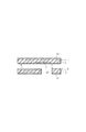
- a first transmission line 2 is formed on a first connection surface 3 that is one surface of a flat plate-like first insulating base material 1 by using a transfer method.
- the first transmission line 2 is embedded in the first insulating substrate 1 and is formed to be flush with the first connection surface 3.
- the first insulating substrate 1 is made of a thermoplastic resin.
- the first transmission line 2 is pressed and embedded in the first insulating base material 1 made of this thermoplastic resin. Thereby, the first substrate unit 4 is manufactured.
- the second transmission line 6 is formed on the second connection surface 7 which is one surface of the flat plate-like second insulating base material 5 by using a transfer method.
- the second transmission line 6 is embedded in the second insulating substrate 5 and is formed to be flush with the second connection surface 7.
- the second insulating substrate 5 is made of a thermoplastic resin. That is, the second transmission line 6 is pressed and embedded in the second insulating base material 5 made of this thermoplastic resin. Thereby, the second substrate unit 8 is manufactured.
- substrate unit 8 are simultaneously performed with the same manufacturing apparatus. It can be carried out. That is, by making the both insulating bases 1 and 5 and the two transmission lines 2 and 6 the same material, they can be simultaneously manufactured by the same manufacturing apparatus. Thereby, both board
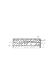
- the first substrate unit 4 and the second substrate unit 8 are connected.
- the first transmission line 2 and the second transmission line 6 formed on both board units 4 and 8 are superposed and thermocompression bonded so that they are in direct contact with each other.
- the pressing operation of the first substrate unit 4 to the second substrate unit 8 at this time is performed in an environment of 300 ° C., for example.
- the wiring connection process for connecting the wirings of the first transmission line 2 and the second transmission line 6 is completed, and the printed circuit board 9 is manufactured.
- the transmission lines 2 and 6 are conductor circuits using, for example, copper.
- the press work for both insulating bases 1 and 5 is performed twice. That is, a press when embedding the transmission lines 2 and 6 by a transfer method and a press at the time of thermocompression bonding in the wiring connection process.
- a press when embedding the transmission lines 2 and 6 by a transfer method and a press at the time of thermocompression bonding in the wiring connection process.
- the insulating bases 1 and 5 are formed of a thermoplastic resin, thereby embedding the transmission lines 2 and 6 in the insulating bases 1 and 5 and forming both connection surfaces 3 and 7 flush with each other. Therefore, it is possible to realize a good connection using thermocompression bonding by bringing both the substrate units 4 and 8 into close contact with each other.
- connection does not involve a connection medium such as a solder ball, Au plating bump, or stud bump, a printed circuit board with good high-frequency characteristics can be obtained.
- a connection medium such as a solder ball, Au plating bump, or stud bump
- a thermoplastic resin having a low dielectric constant of a high frequency signal and good high frequency characteristics.
- the printed circuit board 9 to which the transmission lines 2 and 6 of the circuit board units 4 and 8 are connected can be obtained by a simple manufacturing process.
- FIGS. 3 to 7 another method of manufacturing a printed circuit board according to the present invention will be described in order.
- three substrate units 23, 24, and 25 manufactured by the same material and manufacturing method as the first substrate unit 4 and the second substrate unit 8 described above are prepared.
- the gold plating pad 26 is previously provided in the place which the transmission lines 26 and 27 which oppose should contact. And as shown in FIG. 4, these are laminated
- the substrate unit 25 is on the support plate 27 in order to perform stable thermocompression bonding.
- the gold plating pad 26 connected by crimping is omitted.
- the support plate 27 is removed. Thereafter, the substrate units 23, 24, and 25 are drilled to form through holes 28 that penetrate the substrate units 23, 24, and 25. Then, as shown in FIG. 6, the through hole 28 is plated to form a through hole plating 29. Thereby, what is called an interlayer connection which connects the conductor 30 of the board
- FIG. 7 shows a so-called flex-rigid board in which the protruding part of the board unit 24 is flexible and the laminated part is rigid.
- the manufacturing method according to the present invention can be applied to such a flex-rigid board or a general laminated type printed board, and various effects when using thermocompression bonding can be obtained for each.
- the probe substrate manufacturing method according to the present invention will be described in order with reference to FIGS.
- the first substrate unit 4 and the second substrate unit 8 are manufactured.
- a first conductor circuit 10 is formed on the surface of the first insulating substrate 1 opposite to the surface on which the first transmission line 2 is formed.
- the 2nd conductor circuit 11 is formed in the surface on the opposite side to the surface in which the 2nd transmission line 6 of the 2nd insulating base material 5 is formed.
- Other structures, functions, and effects are the same as in the example of FIG.
- a through hole 12 is formed in the second substrate unit 8.
- the through hole 12 is provided in a portion corresponding to a portion where a bump is formed on the probe substrate, that is, a portion corresponding to an arbitrary portion of the first transmission line 2 when both the substrate units 4 and 8 are connected.
- the two substrate units 4 and 8 are connected by thermocompression using a high temperature (for example, about 300 ° C.) press.
- the reinforcing plate 13 is laminated on the second conductive circuit 11 side of the second substrate unit 8.
- the reinforcing plate 13 is made of, for example, a highly rigid material such as metal, glass epoxy such as FR-4, or the like.
- the reinforcing plate 13 is laminated to increase the mechanical rigidity of the probe substrate and prevent it from being damaged accidentally.
- the reinforcing plate 13 may be provided with a stripline circuit (not shown). Other configurations, operations, and effects are the same as in the example of FIG.
- the through hole 14 is formed so as to penetrate the contact portion between the first transmission line 2 and the second transmission line 6.
- the through hole 14 is formed by drilling with a router or the like.
- the through hole 14 is plated to form a through hole plating 15.
- the conductor thickness of the conductor circuit 10 can be increased by performing through-hole plating.
- the spring property can be reinforced by plating the conductor circuit 10 with nickel or nickel cobalt alloy.
- the first substrate unit 4, the second substrate unit 8, and the reinforcing plate 13 are punched.
- This drilling process is performed by removing the through-hole plating 15 (forming the opening 22), leaving a portion penetrating the contact portion between the first transmission line 2 and the second transmission line 6.
- a resin 16 as an insulating material is filled (embedded) in the opening 22 (see FIG. 13) that has been drilled.
- the first transmission line 2 at the position where the through hole 12 (see FIG. 9) is provided that is, the first transmission line other than the contact portion between the first transmission line 2 and the second transmission line 6.
- the second insulating substrate 5 (reinforcing material 13, second conductor circuit 11, first insulating substrate 1, first conductor circuit 10 if necessary) so that one transmission line 2 is exposed. Notch.
- bumps 17 serving as contact heads are formed on the exposed portions. Thereby, the probe board
- the probe substrate manufactured by the method for manufacturing a probe substrate according to the present invention described above has good high-frequency characteristics and is suitable for use in a high-frequency environment.
- a probe substrate in which a transmission line is formed by a transfer method and a bump is formed on the transmission line is well known, but a portion (second transmission line 6) to be relayed with a coaxial cable is manufactured by the transfer method in order to cope with a high frequency.
- the insulating bases 1 and 5 are formed of a thermoplastic resin
- the transmission lines 2 and 6 are formed flush with the surface, and are brought into close contact with each other so as to be connected by thermocompression bonding. Good characteristics.
- thermoplastic resin as the base material for transfer circuit boards (transmission lines), unlike ordinary thermosetting resins, a fine pitch contact board and a coaxial cable connection board are directly bonded and thermocompression bonded (prepreg, etc.)
- the probe board can be manufactured in a lump.
- through-hole plating, conductive paste (described later), spot welding (described later) to the wiring connection portion of the transfer circuit board it becomes possible to reduce the bump formation process and flip chip process used conventionally, It becomes possible to easily manufacture a probe substrate only with a conventional printed wiring board manufacturing technique. In addition, these can be expected to improve mass production and significantly reduce costs.
- the second insulating substrate 5 and the second conductor circuit 11 are provided with a notch 20 at a location corresponding to the portion where the bump 17 is formed. Then, as shown in FIG. 18, the conductive material 21 is introduced into the recess 19.
- This conductive material may be a conductive paste or a metal by spot welding.
- both substrate units 4 and 8 are thermocompression bonded by a press.
- the connectivity between the first transmission line 2 and the second transmission line 6 is enhanced by the conductive material 21. That is, thermocompression bonding is performed so that the conductive material 21 contacts the first transmission line 2. Thereby, the electrical or mechanical connection between both transmission lines can be ensured.
- the reinforcing portion 13 is punched with a router or the like so that the bumps 17 are exposed to the outside. Furthermore, as shown in FIG.
- substrate 18 is manufactured easily and easily.
- the contact probe 32 of this example is one in which two coaxial cables 33 are connected. These coaxial cables 33 are connected to the second transmission line 6 described above. Corresponding to these coaxial cables 33, bumps 17 are formed at the tips of the contact probes 32, respectively.
- the signal line connected to the bump 17 is the first transmission line 2 described above.
- the transmission lines 2 two central portions of the wiring portion are signal lines 2b and two at both ends are ground lines 2a, and the contact probe 32 is a probe substrate corresponding to a differential signal.
- the bumps 17 are in contact with the object to be inspected to realize electrical contact.
- the land 2c is formed on the first transmission line 2 (ground line 2a, signal line 2b) formed on the first substrate unit 4 used for the contact probe 32. Yes.
- a land 6c is formed in the second transmission line 6 formed in the second substrate unit 8 used for the contact probe 32.
- FIG. 27 shows a probe board corresponding to a 4-channel differential signal.
- SYMBOLS 1 1st insulation base material 2 1st transmission line 3 1st connection surface 4 1st board
- substrate unit DESCRIPTION OF SYMBOLS 9 Printed circuit board 10 1st conductor circuit 11 2nd conductor circuit 12 Through-hole 13 Reinforcement part 14 Through hole 15 Through-hole plating 16 Resin 17 Bump 18 Probe board 19 Recess 20 Notch part 21 Conductive material 22 Opening part 23 Substrate unit 24 board unit 25 board unit 26 gold plating pad 27 support plate 28 through hole 29 through hole plating 30 conductor 31 conductor 32 contact probe 33 coaxial cable
Landscapes
- Engineering & Computer Science (AREA)
- Physics & Mathematics (AREA)
- General Physics & Mathematics (AREA)
- Manufacturing & Machinery (AREA)
- Microelectronics & Electronic Packaging (AREA)
- Structure Of Printed Boards (AREA)
- Production Of Multi-Layered Print Wiring Board (AREA)
Abstract
平板状の第1の絶縁基材(1)を熱可塑性樹脂で形成し、前記第1の絶縁基材(1)の一方の面(3)と面一になるように転写法を用いて第1の伝送線路(2)を形成した第1の基板ユニット(4)を製造する第1の製造工程と、平板状の第2の絶縁基材(5)を熱可塑性樹脂で形成し、前記第2の絶縁基材(5)の一方の面(7)と面一になるように転写法を用いて第2の伝送線路(6)を形成した第2の基板ユニット(8)を製造する第2の製造工程と、前記第1及び第2の基板ユニット(4,8)を前記絶縁基材(1,5)の一方の面(3,7)同士にて重ね合わせて熱圧着し、前記第1の伝送線路(2)と前記第2の伝送線路(6)とを直接に接触させて電気的に接続する配線接続工程とを有する。
Description
本発明は、高周波環境で好適に利用することができるプリント基板の製造方法及びこれを用いたプローブ基板の製造方法に関する。
従来、プリント基板の製造において、一般的な高周波対応製品における配線基板同士の配線接続においては、半田ボール接続、Auスタッドバンプ及びAuめっきバンプによるフリップチップ装置を用いた圧着接続等が用いられている。一般的に、このようなプリント基板が多層プリント配線基板として用いられる場合、配線基板同士を接着層を介して積層し、スルーホールめっきやフィルドビアめっき等による接続が行われる。
一方で、従来、プローブの製造では、微細ピッチコンタクト基板と、同軸ケーブル接続用プリント配線基板とを接続する場合、微細ピッチ配線基板に接続用半田ボール、Auスタッドバンプ、又はAuめっきバンプを作製する。そして、フリップチップ装置を用いてもう一方の基板上に前記微細ピッチ配線基板を熱圧着させ、金属バンプ接続を行う。このような従来技術と同様の技術として、特許文献1に回路基板とその製造方法、その回路基板を用いたバンプ式コンタクトヘッドと半導体部品実装モジュールが開示されている。
しかしながら、従来では、微細ピッチコンタクト基板と同軸ケーブル接続用基板を別々の工程で製造するため、手間がかかり面倒であった。また、プローブ基板においても、一般的なプリント基板においても、半田ボール接続は、接続部分のインピーダンスが不連続となる構造であるため、高周波信号の伝送損失が増大し、高周波信号に対応する基板の製造に用いるための接続技術には向いていない。また、Auバンプを用いたフリップチップ接続法による接続方法は、高価なフリップチップ接続装置を用いるため、設備投資のコストの増大を招く。
本発明は、簡単な構造で高周波信号の損失を低減し、高周波の環境でも好適に対応できるプリント基板の製造方法及びこれを用いたプローブ基板の製造方法を提供する。
本発明では、平板状の第1の絶縁基材を熱可塑性樹脂で形成し、前記第1の絶縁基材の一方の面と面一になるように転写法を用いて第1の伝送線路を形成した第1の基板ユニットを製造する第1の製造工程と、平板状の第2の絶縁基材を熱可塑性樹脂で形成し、前記第2の絶縁基材の一方の面と面一になるように転写法を用いて第2の伝送線路を形成した第2の基板ユニットを製造する第2の製造工程と、前記第1及び第2の基板ユニットを前記絶縁基材の一方の面同士にて重ね合わせて熱圧着し、前記第1の伝送線路と前記第2の伝送線路とを直接に接触させて電気的に接続する配線接続工程とを有することを特徴とするプリント基板の製造方法を提供する。
好ましくは、前記第1の製造工程と前記第2の製造工程を同一の製造装置で同時に行う。
好ましくは、請求項1に記載のプリント基板の製造方法で製造されたプリント基板に対し、前記第1の伝送線路と前記第2の伝送線路との接触部を貫通するスルーホールを形成し、当該スルーホールにめっき処理を施し、前記スルーホールに施しためっきのうち、前記接触部の貫通孔部分を残して前記めっきを除去した開口部を形成し、該開口部に絶縁材を充填し、前記接触部以外の前記第1の伝送線路が露出するように前記第2の絶縁基材を切欠き、前記第1の伝送線路の露出部分にコンタクトヘッドとなるバンプを形成する。
好ましくは、前記第2の基板ユニットに板状の補強板を積層する。
好ましくは、請求項1に記載のプリント基板の製造方法において、前記第1の製造工程で前記第1の伝送線路にコンタクトヘッドとなるバンプを形成し、前記第2の製造工程で前記第2の伝送線路に凹部を形成して、該凹部に導電材を導入する一方、この後の前記配線接続工程にて前記バンプが露出させるべく前記第2の絶縁基材を切欠き、前記配線接続工程で前記導電材が前記第1の伝送線路に接触するように前記第1の伝送線路と前記第2の伝送線路を電気的に接続する。
好ましくは、前記第2の基板ユニットに板状の補強板を積層する。
また好ましくは、前記第1の基板ユニットの伝送線路の絶縁基材裏側の導体厚さは厚い。
また好ましくは、前記第1の基板ユニットの伝送線路の絶縁基材裏側の導体厚さは厚い。
本発明によれば、各基板ユニットの絶縁基材を熱可塑性樹脂で形成し、転写法を用いて各基板ユニットの絶縁基材に形成された各伝送線路を絶縁基材の一方の面と面一になるように形成するので、各伝送線路を直接向かい合わせて密着させて熱圧着を行うことができる。このため、簡単な製造工程で各基板ユニットの伝送線路を接続したプリント基板を得ることができる。また、伝送線路は熱圧着により直接接続されるので、各伝送線路間に半田ボールやAuめっきバンプ、あるいはスタッドバンプを介していない。これにより、高周波特性のよいプリント基板を得ることができる。また、絶縁基材を熱可塑性樹脂で形成するので、転写法を行うときのプレスと、伝送線路の接続を行うときのプレスの計2回のプレスにも耐えることができる。さらに、転写法によって形成された伝送線路は、絶縁基材に埋め込まれているので、上述したように、絶縁基材の一方の面と面一に伝送線路を形成できる。
また、本発明によれば、第1の基板ユニット製造工程と第2の基板ユニット製造工程を同一の製造装置で同時に行うため、迅速かつ効率よく両基板ユニットを形成でき、プリント基板の製造時間を短縮することができる。したがって、プリント基板の生産性が向上する。
また、本発明によれば、第1の伝送線路と第2の伝送線路との接触部にスルーホールを形成し、ここにめっき処理を施す(いわゆるスルーホールめっきを形成する)ため、両伝送線路の接続を強化して確実なものとすることができる。また、第2の絶縁基材を切欠いて露出した第1の伝送線路にバンプを形成するので、簡単かつ容易にプローブ基板を製造することができる。
また、本発明によれば、プローブ基板の機械的な剛性を高めることができ、誤って破損することを抑制できる。
また、本発明によれば、凹部に導電材を導入し、この導電材が第1の伝送線路に接触するように第1の伝送線路と第2の伝送線路を接続するため、両伝送線路の接続を確実なものとすることができる。また、第1の伝送線路にバンプを形成し、予めこのバンプが露出するように第2の絶縁基材を切欠くので、簡単かつ容易にプローブ基板を製造することができる。
また、本発明によれば、プローブ基板の機械的な剛性を高めることができ、誤って破損することを抑制できる。
また、本発明によれば、プローブ基板のコンタクト性能を高めることができ、被測定対象へのコンタクト時に、確実な電気的接触が可能となる。
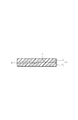
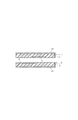
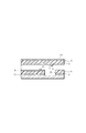
図1に示すように、まず、平板状の第1の絶縁基材1の一方の面である第1の接続面3に対し、転写法を用いて第1の伝送線路2を形成する。この第1の伝送線路2は第1の絶縁基材1に埋め込まれ、第1の接続面3と面一になるように形成される。第1の伝送線路2を埋め込み可能とするため、第1の絶縁基材1は熱可塑性樹脂で形成されている。すなわち、この熱可塑性樹脂からなる第1の絶縁基材1に対し、第1の伝送線路2をプレスして埋め込む。これにより、第1の基板ユニット4が製造される。
他方、平板状の第2の絶縁基材5の一方の面である第2の接続面7に対し、転写法を用いて第2の伝送線路6を形成する。この第2の伝送線路6は第2の絶縁基材5に埋め込まれ、第2の接続面7と面一になるように形成される。第2の伝送線路6を埋め込み可能とするため、第2の絶縁基材5は熱可塑性樹脂で形成されている。すなわち、この熱可塑性樹脂からなる第2の絶縁基材5に対し、第2の伝送線路6をプレスして埋め込む。これにより、第2の基板ユニット8が製造される。
なお、上述した第1の基板ユニット4を製造するための第1の基板ユニット製造工程と、第2の基板ユニット8を製造するための第2の基板ユニット製造工程は、同一の製造装置で同時に行うことができる。すなわち、両絶縁基材1,5や両伝送線路2,6を同一の材料とすることで、同一の製造装置で同時に製造できる。これにより、迅速かつ効率よく両基板ユニット4,8を製造でき、最終的に製造されるプリント基板9(図2参照)の製造時間を短縮することができる。したがって、プリント基板9の生産性が向上する。
次に、図2に示すように、第1の基板ユニット4と第2の基板ユニット8を接続する。この接続は、両基板ユニット4,8に形成された第1の伝送線路2と第2の伝送線路6とが直接接触するように重ね合わされて熱圧着される。このときの第1の基板ユニット4の第2の基板ユニット8へのプレス作業は、例えば300℃の環境下で行われる。このようにして、第1の伝送線路2と第2の伝送線路6との配線を接続するための配線接続工程が完了し、プリント基板9が製造される。なお、伝送線路2,6は、例えば銅を用いた導体回路である。
このプリント基板9の製造に際し、両絶縁基材1,5に対するプレス作業が2回行われている。すなわち、転写法にて伝送線路2,6を埋め込む時のプレスと、配線接続工程での熱圧着時のプレスである。絶縁基材1,5を熱可塑性樹脂で形成することで、計2回のプレスにも耐えることができるものとしている。また、上述したように、絶縁基材1,5を熱可塑性樹脂で形成することで、伝送線路2,6を絶縁基材1,5に埋め込んで両接続面3,7を面一に形成することができるため、両基板ユニット4,8を密着させて熱圧着を用いた良好な接続を実現できる。この接続には、半田ボールやAuめっきバンプ、あるいはスタッドバンプ等の接続媒体を介されていないため、高周波特性がよいプリント基板を得ることができる。このとき、熱可塑性樹脂も高周波信号の誘電率が低く、高周波特性がよいものを用いることが好ましい。以上により、簡単な製造工程で各基板ユニット4,8の伝送線路2,6を接続したプリント基板9を得ることができる。
図3~図7を参照して本発明に係る別のプリント基板の製造方法を順番に説明する。
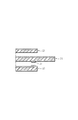
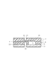
図3に示すように、上述した第1の基板ユニット4や第2の基板ユニット8と同様の材料、製法で製造した基板ユニット23,24,25を3枚用意する。このうち、対向する伝送線路26,27の接触すべき箇所には金めっきパッド26を予め設けておく。そして、図4に示すように、これらを積層して一体化する。この積層は、上述した第1及び第2の基板ユニット4及び8の接続と同様に行われる。このとき、安定した熱圧着を行うために基板ユニット25は支持板27上にある。なお、図4以降では、圧着して接続された金めっきパッド26は省略している。
図3に示すように、上述した第1の基板ユニット4や第2の基板ユニット8と同様の材料、製法で製造した基板ユニット23,24,25を3枚用意する。このうち、対向する伝送線路26,27の接触すべき箇所には金めっきパッド26を予め設けておく。そして、図4に示すように、これらを積層して一体化する。この積層は、上述した第1及び第2の基板ユニット4及び8の接続と同様に行われる。このとき、安定した熱圧着を行うために基板ユニット25は支持板27上にある。なお、図4以降では、圧着して接続された金めっきパッド26は省略している。
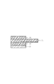
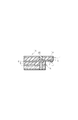
そして、図5に示すように、支持板27を取り外す。その後、基板ユニット23,24,25に穴開け加工を行い、基板ユニット23,24,25を貫通するスルーホール28を形成する。そして、図6に示すように、スルーホール28にめっき処理を施し、スルーホールめっき29を形成する。これにより、基板ユニット23の導体30と、基板ユニット25の導体31とを接続する、いわゆる層間接続ができる。そして、図7に示すように、スルーホールめっき29以外の位置に回路を形成する。具体的には、導体30及び導体31に穴をあけ、回路を形成する。この後、ソルダレジスト等の工程を経て、多層フレキシブルプリント配線板が完成する。図7は、基板ユニット24の突出部分がフレキシブルであり、積層部分がリジッドである、いわゆるフレックスリジッド基板を示している。本発明に係る製造方法は、このようなフレックスリジット基板や、一般的な積層タイプのプリント基板に適用でき、熱圧着を用いたときの様々な効果もそれぞれについて得ることができる。
図8~図15を参照して本発明に係るプローブ基板の製造方法を順番に説明する。
図8に示すように、第1の基板ユニット4及び第2の基板ユニット8を製造する。第1の絶縁基材1の第1の伝送線路2が形成される面と反対側の面には、第1の導体回路10が形成される。同様に、第2の絶縁基材5の第2の伝送線路6が形成される面と反対側の面には、第2の導体回路11が形成される。その他の構造、作用、効果は図1の例と同様である。次に、図9に示すように、第2の基板ユニット8に貫通孔12を形成する。この貫通孔12は、プローブ基板におけるバンプを形成する部分に相当する箇所、すなわち両基板ユニット4,8を接続したときに第1の伝送線路2の任意の箇所と対応する部分に設けられる。
図8に示すように、第1の基板ユニット4及び第2の基板ユニット8を製造する。第1の絶縁基材1の第1の伝送線路2が形成される面と反対側の面には、第1の導体回路10が形成される。同様に、第2の絶縁基材5の第2の伝送線路6が形成される面と反対側の面には、第2の導体回路11が形成される。その他の構造、作用、効果は図1の例と同様である。次に、図9に示すように、第2の基板ユニット8に貫通孔12を形成する。この貫通孔12は、プローブ基板におけるバンプを形成する部分に相当する箇所、すなわち両基板ユニット4,8を接続したときに第1の伝送線路2の任意の箇所と対応する部分に設けられる。
次に、図10に示すように、高温(例えば約300℃)プレスによる熱圧着を用いて、両基板ユニット4,8を接続する。このとき、第2の基板ユニット8の第2の導電回路11側に、補強板13が積層される。この補強板13は、例えば金属等の剛性の高い材料や、FR-4等のガラスエポキシ等で形成されている。一般に、プローブ基板を製造する工程において、熱可塑性樹脂からなる基板ユニット4,8は薄いので、プローブ基板の機械的な剛性を高め、誤って破損することを抑制するために補強板13が積層される。この補強板13にはストリップラインの回路(不図示)を設けてもよい。その他の構成、作用、効果は図2の例と同様である。
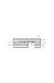
次に、図11に示すように、第1の伝送線路2と第2の伝送線路6との接触部を貫通するようにスルーホール14を形成する。このスルーホール14はルータ等により穴開け加工されて形成される。そして、図12に示すように、スルーホール14内にめっき処理を施して、スルーホールめっき15を形成する。このとき、スルーホールめっきを行うことで、導体回路10の導体厚さを厚くすることもできる。また、ニッケルやニッケルコバルト合金などを導体回路10にめっきすることで、バネ性を補強することもできる。そして、図13に示すように、第1の基板ユニット4、第2の基板ユニット8、補強板13に対して穴開け加工をする。この穴開け加工は、第1の伝送線路2と第2の伝送線路6との接触部を貫通する部分を残して、スルーホールめっき15を除去して行われる(開口部22を形成する)。これにより、第1の伝送線路2と第2の伝送線路6はその重なりあった接触部において、スルーホールめっきを介して接続されるため、接続が強化されて確実となる。すなわち、熱圧着によるプレス接続に加えて、スルーホールめっきによる接続も施される。
次に、図14に示すように、穴開け加工された開口部22(図13参照)に絶縁材たる樹脂16を充填する(埋め込む)。そして、図15に示すように、貫通孔12(図9参照)を設けた位置の第1の伝送線路2、すなわち第1の伝送線路2と第2の伝送線路6との接触部以外の第1の伝送線路2が露出するように、第2の絶縁基材5(必要であれば補強材13、第2の導体回路11、第1の絶縁基材1、第1の導体回路10)を切欠く。そして、露出部分にコンタクトヘッドとなるバンプ17を形成する。これにより、簡単かつ容易にプローブ基板18が製造される。
以上説明した本発明に係るプローブ基板の製造方法で製造されたプローブ基板は、高周波特性がよく、高周波環境での使用に対応するものである。転写法で伝送線路を形成し、これにバンプを形成したプローブ基板は公知であるが、高周波に対応させるために同軸ケーブルと中継させる部分(第2の伝送線路6)を転写法で製造することは、構造上困難であった。しかしながら、本発明では、絶縁基材1,5を熱可塑性樹脂で形成し、この表面と面一に伝送線路2,6を形成し、互いを密着させて熱圧着して接続することで、高周波特性を良好なものとしている。
なお、本発明に係るプローブ基板の製造方法の効果を、上記と重複する記載もあるが、以下に説明する。熱可塑性樹脂を転写回路基板(伝送線路)の基材とすることで、通常の熱硬化性樹脂とは異なり、微細ピッチコンタクト基板と同軸ケーブル接続用基板を直接貼り合わせて熱圧着し(プリプレグ等が不要となる)、一括でプローブ基板の製造が可能となる。また、転写回路基板の配線接続部分にスルーホールめっき、導電性ペースト(後述)、スポット溶接(後述)を用いて接続することによって、従来用いたバンプ形成工程及びフリップチップ工程の削減が可能となり、従来のプリント配線板の製造技術のみで簡便にプローブ基板を製造することが可能となる。また、これらにより、量産化の向上、コストの大幅な削減が期待できる。
図16~図21を参照して本発明に係る別のプローブ基板の製造方法を順番に説明する。なお、同一の作用、効果を奏するものについては、上述したものと同一の符号を付して説明する。
図16に示すように、第1の基板ユニット4及び第2の基板ユニット8を製造する。このとき、第1の伝送線路2にコンタクトヘッドとなるバンプ17を形成する。なお、この例では、補強材13をこの時点で積層している。その他の構造、作用、効果は図8の例と同様である。次に、図17に示すように、第2の伝送線路6に凹部19を形成する。また、第2の絶縁基材5及び第2の導体回路11には、バンプ17が形成された部分に相当する箇所に切欠き部20が形成される。そして、図18に示すように、凹部19に、導電材21が導入される。この導電材は、導電性ペーストでもよいし、スポット溶接による金属でもよい。
図16に示すように、第1の基板ユニット4及び第2の基板ユニット8を製造する。このとき、第1の伝送線路2にコンタクトヘッドとなるバンプ17を形成する。なお、この例では、補強材13をこの時点で積層している。その他の構造、作用、効果は図8の例と同様である。次に、図17に示すように、第2の伝送線路6に凹部19を形成する。また、第2の絶縁基材5及び第2の導体回路11には、バンプ17が形成された部分に相当する箇所に切欠き部20が形成される。そして、図18に示すように、凹部19に、導電材21が導入される。この導電材は、導電性ペーストでもよいし、スポット溶接による金属でもよい。
そして、図19に示すように、両基板ユニット4,8をプレスにより熱圧着する。このとき、導電材21により、第1の伝送線路2と第2の伝送線路6との接続性が強化される。すなわち、導電材21が第1の伝送線路2に接触するように、熱圧着される。これにより、両伝送線路の電気的あるいは機械的接続を確実なものとすることができる。その他のプレス時の作用、効果は図10の例と同様である。そして、図20に示すように、バンプ17が外部に露出するように、補強部13をルータ等で穴開け加工する。さらに、図21に示すように、プローブ基板18としての外形を整えるため、第2の絶縁基材5、補強材13、第2の導体回路11、第1の絶縁基材1、第1の導体回路10を切欠く。これにより、簡単かつ容易にプローブ基板18が製造される。
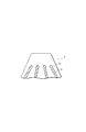
図22に示すように、この例のコンタクトプローブ32は、同軸ケーブル33が2本接続されたものである。これらの同軸ケーブル33は、上述した第2の伝送線路6と接続されている。これらの同軸ケーブル33に対応して、コンタクトプローブ32の先端にはそれぞれバンプ17が形成されている。図23において、バンプ17と接続された信号線は上述した第1の伝送線路2である。この伝送線路2のうち、配線部の中央部2本が信号線2b、両端の2本がグラウンド線2aとなり、コンタクトプローブ32は差動信号に対応するプローブ基板となる。バンプ17は、被検査体と接触して電気コンタクトを実現する。
また、図24を参照すれば、コンタクトプローブ32に用いられている第1の基板ユニット4に形成された第1の伝送線路2(グラウンド線2a、信号線2b)にはランド2cが形成されている。一方、図25を参照すれば、コンタクトプローブ32に用いられている第2の基板ユニット8に形成された第2の伝送線路6にはランド6cが形成されている。そしてこれら4,8は、上述したように熱圧着により重ね合わされているが、これを平面でみると図26に示すように、互いのランド2c、6cにて重なり合った部分に接続部16が形成されている。
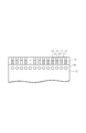
また、図27のように、信号線2bを2本配し、その両側にグラウンド線2aを2本配し、この組み合わせを並べて繰り返すことで、多チャンネルの差動信号に対応するプローブ基板(コンタクトプローブ32)が形成される。例えば、図27は4チャンネルの差動信号に対応するプローブ基板である。
1 第1の絶縁基材
2 第1の伝送線路
3 第1の接続面
4 第1の基板ユニット
5 第2の絶縁基材
6 第2の伝送線路
7 第2の接続面
8 第2の基板ユニット
9 プリント基板
10 第1の導体回路
11 第2の導体回路
12 貫通孔
13 補強部
14 スルーホール
15 スルーホールめっき
16 樹脂
17 バンプ
18 プローブ基板
19 凹部
20 切欠き部
21 導電材
22 開口部
23 基板ユニット
24 基板ユニット
25 基板ユニット
26 金めっきパッド
27 支持板
28 スルーホール
29 スルーホールめっき
30 導体
31 導体
32 コンタクトプローブ
33 同軸ケーブル
2 第1の伝送線路
3 第1の接続面
4 第1の基板ユニット
5 第2の絶縁基材
6 第2の伝送線路
7 第2の接続面
8 第2の基板ユニット
9 プリント基板
10 第1の導体回路
11 第2の導体回路
12 貫通孔
13 補強部
14 スルーホール
15 スルーホールめっき
16 樹脂
17 バンプ
18 プローブ基板
19 凹部
20 切欠き部
21 導電材
22 開口部
23 基板ユニット
24 基板ユニット
25 基板ユニット
26 金めっきパッド
27 支持板
28 スルーホール
29 スルーホールめっき
30 導体
31 導体
32 コンタクトプローブ
33 同軸ケーブル
Claims (7)
- 平板状の第1の絶縁基材を熱可塑性樹脂で形成し、前記第1の絶縁基材の一方の面と面一になるように転写法を用いて第1の伝送線路を形成した第1の基板ユニットを製造する第1の製造工程と、
平板状の第2の絶縁基材を熱可塑性樹脂で形成し、前記第2の絶縁基材の一方の面と面一になるように転写法を用いて第2の伝送線路を形成した第2の基板ユニットを製造する第2の製造工程と、
前記第1及び第2の基板ユニットを前記絶縁基材の一方の面同士にて重ね合わせて熱圧着し、前記第1の伝送線路と前記第2の伝送線路とを直接に接触させて電気的に接続する配線接続工程とを有することを特徴とするプリント基板の製造方法。 - 前記第1の製造工程と前記第2の製造工程を同一の製造装置で同時に行うことを特徴とする請求項1に記載のプリント基板の製造方法。
- 請求項1に記載のプリント基板の製造方法で製造されたプリント基板に対し、前記第1の伝送線路と前記第2の伝送線路との接触部を貫通するスルーホールを形成し、
当該スルーホールにめっき処理を施し、
前記スルーホールに施しためっきのうち、前記接触部の貫通孔部分を残して前記めっきを除去した開口部を形成し、
該開口部に絶縁材を充填し、
前記接触部以外の前記第1の伝送線路が露出するように前記第2の絶縁基材を切欠き、
前記第1の伝送線路の露出部分にコンタクトヘッドとなるバンプを形成することを特徴とするプローブ基板の製造方法。 - 前記第2の基板ユニットに板状の補強板を積層することを特徴とする請求項3に記載のプローブ基板の製造方法。
- 請求項1に記載のプリント基板の製造方法において、前記第1の製造工程で前記第1の伝送線路にコンタクトヘッドとなるバンプを形成し、前記第2の製造工程で前記第2の伝送線路に凹部を形成して、該凹部に導電材を導入する一方、この後の前記配線接続工程にて前記バンプが露出させるべく前記第2の絶縁基材を切欠き、前記配線接続工程で前記導電材が前記第1の伝送線路に接触するように前記第1の伝送線路と前記第2の伝送線路を電気的に接続することを特徴とするプローブ基板の製造方法。
- 前記第2の基板ユニットに板状の補強板を積層することを特徴とする請求項5に記載のプローブ基板の製造方法。
- 前記第1の基板ユニットの伝送線路の絶縁基材裏側の導体厚さを厚くすることを特徴とする請求項1に記載のプローブ基板の製造方法。
Priority Applications (1)
| Application Number | Priority Date | Filing Date | Title |
|---|---|---|---|
| JP2011547685A JP5582618B2 (ja) | 2009-12-28 | 2010-12-27 | プローブ基板の製造方法 |
Applications Claiming Priority (2)
| Application Number | Priority Date | Filing Date | Title |
|---|---|---|---|
| JP2009297327 | 2009-12-28 | ||
| JP2009-297327 | 2009-12-28 |
Publications (1)
| Publication Number | Publication Date |
|---|---|
| WO2011081129A1 true WO2011081129A1 (ja) | 2011-07-07 |
Family
ID=44226534
Family Applications (1)
| Application Number | Title | Priority Date | Filing Date |
|---|---|---|---|
| PCT/JP2010/073529 Ceased WO2011081129A1 (ja) | 2009-12-28 | 2010-12-27 | プリント基板の製造方法及びこれを用いたプローブ基板の製造方法 |
Country Status (2)
| Country | Link |
|---|---|
| JP (1) | JP5582618B2 (ja) |
| WO (1) | WO2011081129A1 (ja) |
Cited By (1)
| Publication number | Priority date | Publication date | Assignee | Title |
|---|---|---|---|---|
| JP2020041963A (ja) * | 2018-09-13 | 2020-03-19 | 東京特殊電線株式会社 | 半導体デバイス検査用多芯プローブユニット及びその製造方法 |
Citations (6)
| Publication number | Priority date | Publication date | Assignee | Title |
|---|---|---|---|---|
| JPS6365638A (ja) * | 1986-09-05 | 1988-03-24 | テクトロニクス・インコーポレイテツド | 集積回路ウエハ・プローブ装置 |
| JPS63152141A (ja) * | 1986-12-16 | 1988-06-24 | Nec Corp | プロ−ブカ−ド |
| JPH06152138A (ja) * | 1992-11-11 | 1994-05-31 | Hitachi Chem Co Ltd | 多層配線板 |
| JPH09330995A (ja) * | 1995-10-13 | 1997-12-22 | Meiko:Kk | 回路基板とその製造方法、その回路基板を用いたバンプ式コンタクトヘッドと半導体部品実装モジュール |
| JP2004343055A (ja) * | 2003-04-25 | 2004-12-02 | Hitachi Chem Co Ltd | 微細接続抵抗評価用パターンおよび部材とその製造方法とそれを用いた評価方法、ならびに多層板 |
| JP2005012135A (ja) * | 2003-06-23 | 2005-01-13 | Fuchigami Micro:Kk | 多層回路基板及びその製造方法 |
-
2010
- 2010-12-27 JP JP2011547685A patent/JP5582618B2/ja not_active Expired - Fee Related
- 2010-12-27 WO PCT/JP2010/073529 patent/WO2011081129A1/ja not_active Ceased
Patent Citations (6)
| Publication number | Priority date | Publication date | Assignee | Title |
|---|---|---|---|---|
| JPS6365638A (ja) * | 1986-09-05 | 1988-03-24 | テクトロニクス・インコーポレイテツド | 集積回路ウエハ・プローブ装置 |
| JPS63152141A (ja) * | 1986-12-16 | 1988-06-24 | Nec Corp | プロ−ブカ−ド |
| JPH06152138A (ja) * | 1992-11-11 | 1994-05-31 | Hitachi Chem Co Ltd | 多層配線板 |
| JPH09330995A (ja) * | 1995-10-13 | 1997-12-22 | Meiko:Kk | 回路基板とその製造方法、その回路基板を用いたバンプ式コンタクトヘッドと半導体部品実装モジュール |
| JP2004343055A (ja) * | 2003-04-25 | 2004-12-02 | Hitachi Chem Co Ltd | 微細接続抵抗評価用パターンおよび部材とその製造方法とそれを用いた評価方法、ならびに多層板 |
| JP2005012135A (ja) * | 2003-06-23 | 2005-01-13 | Fuchigami Micro:Kk | 多層回路基板及びその製造方法 |
Cited By (1)
| Publication number | Priority date | Publication date | Assignee | Title |
|---|---|---|---|---|
| JP2020041963A (ja) * | 2018-09-13 | 2020-03-19 | 東京特殊電線株式会社 | 半導体デバイス検査用多芯プローブユニット及びその製造方法 |
Also Published As
| Publication number | Publication date |
|---|---|
| JP5582618B2 (ja) | 2014-09-03 |
| JPWO2011081129A1 (ja) | 2013-05-13 |
Similar Documents
| Publication | Publication Date | Title |
|---|---|---|
| US7990165B2 (en) | Contact probe and method of making the same | |
| JP2500462B2 (ja) | 検査用コネクタおよびその製造方法 | |
| EP1005086B1 (en) | Metal foil having bumps, circuit substrate having the metal foil, and semiconductor device having the circuit substrate | |
| JP5010737B2 (ja) | プリント配線板 | |
| JP4058607B2 (ja) | 配線基板及びその製造方法、電子部品、回路基板並びに電子機器 | |
| JP2001177045A (ja) | 半導体装置及びその製造方法 | |
| US7985926B2 (en) | Printed circuit board and electronic component device | |
| US11510315B2 (en) | Multilayer substrate, interposer, and electronic device | |
| JP4070470B2 (ja) | 半導体装置用多層回路基板及びその製造方法並びに半導体装置 | |
| JP2008016817A (ja) | 埋立パターン基板及びその製造方法 | |
| CN102904082A (zh) | 连接器结构及其制作方法 | |
| JP5009576B2 (ja) | 半導体装置の製造方法 | |
| US7963031B2 (en) | Package for semiconductor device and method of manufacturing the same | |
| KR100628418B1 (ko) | 반도체 장치 및 반도체 장치의 제조 방법 | |
| JP5582618B2 (ja) | プローブ基板の製造方法 | |
| JP2007201175A (ja) | 半導体装置およびそれを備えた電子機器、およびそれに用いる半導体装置用基板の製造方法 | |
| JP7351552B2 (ja) | 基板、基板製造方法及び基板接続方法 | |
| TW202238915A (zh) | 球接合阻抗匹配 | |
| CN116963394B (zh) | 嵌埋连接器的电路板及其制作方法 | |
| JP2009278050A (ja) | 電子モジュール、配線板、電子モジュールの製造方法、配線板の製造方法 | |
| CN100499054C (zh) | 半导体装置及其制造方法 | |
| JP2011035211A (ja) | 部品実装モジュール、部品実装モジュール内蔵配線板、部品実装モジュール内蔵配線板の製造方法 | |
| JP2009147066A (ja) | 部品内蔵配線板、部品内蔵配線板の製造方法 | |
| JP2005217030A (ja) | リジットフレックス基板及びその製造方法並びに補修方法 | |
| TWI293236B (en) | Method for manufacturing a substrate embedded with an electronic component and device from the same |
Legal Events
| Date | Code | Title | Description |
|---|---|---|---|
| 121 | Ep: the epo has been informed by wipo that ep was designated in this application |
Ref document number: 10840985 Country of ref document: EP Kind code of ref document: A1 |
|
| WWE | Wipo information: entry into national phase |
Ref document number: 2011547685 Country of ref document: JP |
|
| NENP | Non-entry into the national phase |
Ref country code: DE |
|
| 122 | Ep: pct application non-entry in european phase |
Ref document number: 10840985 Country of ref document: EP Kind code of ref document: A1 |