WO2011078015A1 - 板状部材の揺動装置 - Google Patents
板状部材の揺動装置 Download PDFInfo
- Publication number
- WO2011078015A1 WO2011078015A1 PCT/JP2010/072482 JP2010072482W WO2011078015A1 WO 2011078015 A1 WO2011078015 A1 WO 2011078015A1 JP 2010072482 W JP2010072482 W JP 2010072482W WO 2011078015 A1 WO2011078015 A1 WO 2011078015A1
- Authority
- WO
- WIPO (PCT)
- Prior art keywords
- voltage
- electrode
- plate
- movable
- row
- Prior art date
- Legal status (The legal status is an assumption and is not a legal conclusion. Google has not performed a legal analysis and makes no representation as to the accuracy of the status listed.)
- Ceased
Links
Images







Classifications
-
- G—PHYSICS
- G02—OPTICS
- G02B—OPTICAL ELEMENTS, SYSTEMS OR APPARATUS
- G02B26/00—Optical devices or arrangements for the control of light using movable or deformable optical elements
- G02B26/08—Optical devices or arrangements for the control of light using movable or deformable optical elements for controlling the direction of light
- G02B26/0816—Optical devices or arrangements for the control of light using movable or deformable optical elements for controlling the direction of light by means of one or more reflecting elements
- G02B26/0833—Optical devices or arrangements for the control of light using movable or deformable optical elements for controlling the direction of light by means of one or more reflecting elements the reflecting element being a micromechanical device, e.g. a MEMS mirror, DMD
- G02B26/0841—Optical devices or arrangements for the control of light using movable or deformable optical elements for controlling the direction of light by means of one or more reflecting elements the reflecting element being a micromechanical device, e.g. a MEMS mirror, DMD the reflecting element being moved or deformed by electrostatic means
-
- G—PHYSICS
- G09—EDUCATION; CRYPTOGRAPHY; DISPLAY; ADVERTISING; SEALS
- G09G—ARRANGEMENTS OR CIRCUITS FOR CONTROL OF INDICATING DEVICES USING STATIC MEANS TO PRESENT VARIABLE INFORMATION
- G09G3/00—Control arrangements or circuits, of interest only in connection with visual indicators other than cathode-ray tubes
- G09G3/20—Control arrangements or circuits, of interest only in connection with visual indicators other than cathode-ray tubes for presentation of an assembly of a number of characters, e.g. a page, by composing the assembly by combination of individual elements arranged in a matrix no fixed position being assigned to or needed to be assigned to the individual characters or partial characters
- G09G3/34—Control arrangements or circuits, of interest only in connection with visual indicators other than cathode-ray tubes for presentation of an assembly of a number of characters, e.g. a page, by composing the assembly by combination of individual elements arranged in a matrix no fixed position being assigned to or needed to be assigned to the individual characters or partial characters by control of light from an independent source
Definitions
- a plurality of movable units including plate-like members whose postures can be changed are arranged in a matrix in the row direction and the column direction.
- the posture of the plate-like member is switched for each movable unit independently of the other movable units.
- a drive is required.
- row electrodes for rows in which the postures of the plate-like members are switched using row electrodes that exist independently for the number of rows and column electrodes that exist independently for the number of columns are used.
- the plate member does not change its posture even when ⁇ 5 V or +5 V is applied to the column electrode.
- an arbitrary intersection point can be selected and the posture of the plate-like member can be switched to the intended posture, and the posture of the plate-like member at another intersection point is not changed by the operation.
- the posture of the plate-like member is switched independently of the other movable units for each movable unit with respect to all the movable units of the matrix type device. It becomes possible.
- the first and second lines cannot be controlled independently.
- the processing for a specific row when the processing for a specific row is completed, it is necessary to switch to a state in which the new processing for that row is prohibited. This processing takes time, and the processing start time for the next row is delayed.
- This specification discloses a technique that enables processing for the next line without switching to a state in which new processing for that line is prohibited when processing for a specific line is completed. For this reason, this specification discloses a movable unit in which a new process is prohibited by the completion of the process itself without switching to a state in which the new process is prohibited in the movable unit that has completed the process. . If a movable unit having this property is obtained, there is no need to switch to a state in which new processing is prohibited. When a one-dimensional array type device or a two-dimensional matrix type device is configured with a movable unit having such characteristics, the advantage of not having to switch to a state in which new processing is prohibited becomes obvious. In this specification, a technique effective for a movable unit as a unit is disclosed, and a technique effective for an array type device and a matrix type device using a plurality of the movable units is disclosed.
- the apparatus includes a substrate, a support portion, a movable beam, a plate-like member, a first electrode, a second electrode, and a drive circuit.
- the support portion is fixed to the substrate and extends upward from the substrate.
- the movable beam connects the support portion and the plate-like member, supports the plate-like member so as to be swingable around the swing axis, and returns the plate-like member to a posture parallel to the substrate. Demonstrate.
- the plate-like member has a first end and a second end facing each other across the swing shaft, and at least a part thereof is formed of a conductor.
- the first electrode is formed on the substrate at a position facing the first end.
- the second electrode is formed on the substrate at a position facing the second end.
- the drive circuit applies one of the first voltage and the second voltage to the plate-like member, applies one of the third voltage and the fourth voltage to the first electrode, and applies the first voltage to the second electrode. The other of the three voltages and the fourth voltage is applied. The restrictions on the first to fourth voltages will be described later.
- the distance between the first end and the first electrode and the distance between the second end and the second electrode when the plate-like member is in a posture parallel to the substrate are d0.
- the proximity distance when the plate-like member swings and the distance between the first end and the first electrode approaches is d1
- the separation distance when the distance between the second end and the second electrode is separated is Let d2.
- the proximity distance is d1
- the distance between the first end and the first electrode is increased.
- the separation distance be d2.
- the first voltage to the fourth voltage satisfy the following relationships (1) to (3). (1) The distance between the first end and the first electrode and the distance between the second end and the second electrode are d0, the first voltage is applied to the plate member, and the third voltage and the fourth are applied to the first electrode.
- the plate-like member When the plate-like member is swung so as to approach the first electrode, the distance between the first end and the first electrode approaches the proximity distance d1, and the distance between the second end and the second electrode separates to the separation distance d2.
- the plate-like member When the plate-like member is swung so as to approach the second electrode, the distance between the second end and the second electrode approaches the proximity distance d1, and the distance between the first end and the first electrode increases to the separation distance d2. To do. That is, the plate-like member has a seesaw structure.
- the relationship of (1) will be described.
- the electrostatic attractive force acting between the first electrode and the plate-like member becomes the torque that causes the plate-like member to swing around the swing axis, and the electrostatic attractive force acting between the second electrode and the plate-like member is plate-like. This is a torque for swinging the member around the swing shaft. Since the directions of the torques of the two are opposite, the difference between the torques of the two becomes an effective torque for swinging the plate member.
- the magnitude of the electrostatic attractive force acting between the end of the plate member and the electrode is proportional to the square of the voltage difference between the end and the electrode, and inversely proportional to the square of the distance between the end and the electrode.
- the distance between the first end and the first electrode and the distance between the second end and the second electrode are both d0. That is, it is in a state where a large electrostatic attraction can be obtained as compared with the case where the distance between the end portion and the electrode is separated (when d2 is reached).
- the relationship of (1) is that when a third voltage is applied to one electrode and a fourth voltage is applied to the other electrode in a state where a large electrostatic attractive force is obtained, the torque difference applied to the plate-like member gives a restoring force. This means that the plate-like member swings by deforming the movable beam.
- the voltage difference between the third voltage and the fourth voltage is the movable beam. It means that it is large enough to produce an effective torque that exceeds the return force.
- the relationship (2) will be described.
- the movable unit is required not to be processed even if another movable unit is selected and processed, but to be processed unless the movable unit is selected and processed. From the relationship (1), when the first voltage is applied to the plate-like member of the movable unit to be processed, the processing for the movable unit becomes possible.
- the first electrode and the second electrode are independent of the voltage applied to the first electrode and the second electrode. Since the difference in torque applied to the plate is less than the restoring force of the movable beam, the plate-like member does not swing and maintains a posture parallel to the substrate.
- the movable unit to which the second voltage is applied is not applied.
- the plate member does not swing. Even if another movable unit is selected and processed, it is not processed, and unless the movable unit is selected and processed, it is not processed. Further, the movable unit is required to have a property of returning the processed movable unit to the state before the processing.
- the plate-like member is returned to a posture parallel to the substrate without depending on the voltage state of the first electrode and the second electrode. Is possible.
- the plate member Prior to rocking the plate member using the relationship (1), the plate member can be returned to a posture parallel to the substrate. It is possible to perform the process of swinging the plate-like member in a state where an electrostatic attractive force larger than that in the case of d0 and the separation distance d2 is obtained.
- the relationship (3) will be described.
- the plate-like member is swung in the movable unit, it is preferable that the swinging posture is not reversed even if a voltage for swinging the plate-like member in the opposite direction is applied to the first electrode and the second electrode. If this is possible, a new process is prohibited for a processed movable unit when the process of switching the swing state of a certain movable unit is followed by a process of switching the swing state of another movable unit. This is because it is not necessary to switch to the state to be performed.
- the third voltage is larger than the first voltage and the fourth voltage, the first voltage is applied to the plate-like member, the third voltage is applied to the first electrode, and the second electrode is applied from the relationship (1).
- the plate-like member approaches the first electrode and its distance becomes d1, and the plate-like member separates from the second electrode and its distance becomes d2.
- the swinging direction of the plate-shaped member is not reversed.
- the swinging direction of the plate member may be reversed. For example, it is necessary to switch to a state in which new processing is prohibited for the processed movable unit before switching the swing state of the other movable units.
- the first voltage is applied to the plate-like member
- the fourth voltage is applied to the first electrode
- the plate-like member is swung in the relationship (3), the swinging posture is reversed even if a voltage for swinging the plate-like member in the opposite direction is applied to the first electrode and the second electrode. In a state in which a new process is prohibited for a processed movable unit after the process of switching the swing state of a certain movable unit until the swing state of another movable unit is switched. There is no need to switch to.
- the plate member can be swung by the voltage applied to the first electrode and the second electrode by applying the first voltage to the plate member according to the relationship (1), and (2) Therefore, by applying the second voltage to the plate-like member, the plate-like member is returned to the posture parallel to the substrate without depending on the voltage applied to the first electrode and the second electrode, or to the posture parallel to the substrate.
- the first voltage is applied to the other movable unit in the state where the first voltage is continuously applied to the plate unit of the movable unit in which the plate member is oscillating. Even if a voltage that reverses the swinging direction of the plate member is applied to the electrode and the second electrode, the swinging direction of the plate member does not reverse.
- the movable unit that has finished processing can obtain a characteristic in which the new processing is prohibited by switching the processing itself without switching to a state in which the new processing is prohibited.
- the above devices have various applications. For example, it is possible to realize an optical deflecting device that changes the reflection direction of a light beam by forming a mirror on a plate-like member. In addition, it is possible to realize a storage device that changes and stores the capacitance between the plate-like member and the electrode. It is also possible to realize a relay device that switches a contact switch by a swinging plate-like member.
- An apparatus having a plurality of movable units has the following configuration.
- a plurality of movable units composed of a movable beam, a plate-like member, a first electrode, and a second electrode are arranged, and the first electrode of each movable unit is connected to a drive circuit in common, and each movable unit
- the second electrodes are commonly connected to the drive circuit, and the plate-like members of each movable unit are individually connected to the drive circuit.
- the voltage difference between the third voltage and the first voltage is adjusted to be larger than the voltage difference between the fourth voltage and the first voltage.
- the drive circuit selects one movable unit from among the movable unit in which the plate-like member is oscillating and the movable unit in which the plate-like member is not oscillated, and the first circuit is selected as the selected movable unit.
- a voltage is applied, a second voltage is applied to the plate-like member of the other movable unit, and one of the third voltage and the fourth voltage is commonly applied to the first electrodes of the plurality of movable units.
- the other voltage of the third voltage and the fourth voltage is applied in common to the second electrodes of the plurality of movable units. Then, the following event occurs in the plurality of movable units.
- the movable unit to be processed is selected from the movable units in which the plate-shaped member is not swung, and the plate-shaped member is swung.
- the first voltage is applied to the plate-like member
- one of the third voltage and the fourth voltage is applied to the first electrode
- the third voltage and the fourth voltage are applied to the second electrode. Apply the other voltage.
- the plate member swings in a direction approaching the electrode to which the third voltage is applied.
- the event (b) is a movable unit in which the plate-shaped member is not rocked, and does not rock the plate-shaped member of the movable unit that is not the object of processing.
- the second voltage is applied to the plate-like member of the movable unit that is not the object of processing.
- a process in which the second voltage is applied to the plate-like member even when one of the third voltage and the fourth voltage is applied to the first electrode and the other voltage is applied to the second electrode.
- the plate member of the movable unit that is not the target does not swing.
- the event (c) is stored while maintaining the swinging posture in the movable unit in which the plate-like member has been swinging. Specifically, the swinging posture is maintained by applying the first voltage to the plate-like member.
- the plate member swings in a direction approaching the first electrode.
- the oscillating direction is not reversed.
- a fourth voltage is applied to the first electrode and a third voltage is applied to the second electrode in order to swing the plate-like member of another movable unit, it swings in a direction approaching the first electrode.
- the plate-like member thus maintained maintains its posture.
- the plate member returns to a posture parallel to the substrate. As a result, the swinging plate-like member can be returned to a posture in which it does not swing.
- the first voltage cannot be applied to the plate member of a new movable unit unless the voltage applied to the processed plate member is switched from the first voltage to the second voltage. There is no. As a result, the time required to process a plurality of movable units can be shortened, and the drive circuit can be simplified.
- the technique disclosed in this specification is particularly useful when a plurality of movable units are arranged in a matrix in the row direction and the column direction.
- the following configuration is adopted.
- (1) The swing shaft provided in each movable unit extends in the column direction.
- (2) The first electrodes of the movable units arranged in the column direction are commonly connected to the drive circuit.
- (3) The first electrodes of the movable units having different columns are individually connected to the drive circuit.
- the second electrodes of the movable units arranged in the column direction are commonly connected to the drive circuit.
- the second electrodes of the movable units having different columns are individually connected to the drive circuit.
- the plate members of movable units arranged in the row direction are connected to the drive circuit in common.
- the plate-like electrodes of the movable units having different rows are individually connected to the drive circuit.
- the drive circuit performs the following operations.
- a processed row and one row to be processed are selected, the first voltage is applied to the plate member of the movable unit belonging to the selected row, and the plate shape of the movable unit belonging to the other rows
- a second voltage is applied to the member.
- B) In one row to be processed the third voltage is applied to the first electrode and the fourth voltage is applied to the second electrode in the column in which the plate-like member is brought close to the first electrode, and the second electrode is applied to the second electrode. In the row in which the plate-like members are approached, the fourth voltage is applied to the first electrode and the third voltage is applied to the second electrode.
- C) The voltage applied to the plate member at a predetermined time is switched from the first voltage to the second voltage.
- a two-dimensional matrix is formed by arranging the movable units in the row direction and the column direction. And the attitude
- An arbitrary pattern can be formed by movable units formed in a two-dimensional matrix. Since there is no restriction that the first voltage cannot be applied to other rows after the voltage applied to the processed row has been switched from the first voltage to the second voltage, the processing for all the movable units is completed. Time is shortened.
- the second voltage and the fourth voltage can be the ground voltage.
- applying the second voltage means grounding and means not applying a voltage.
- applying the fourth voltage means grounding, and means applying no voltage.
- the third voltage is a negative voltage. If the first voltage is a negative voltage, the third voltage is a positive voltage.
- the writing time can be shortened and the driving circuit can be simplified.
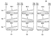
- FIG. 3 is a schematic diagram (part 1) of a matrix portion according to the first embodiment.
- FIG. 6 is a schematic diagram (part 2) of the matrix portion of the first embodiment.
- FIG. 6 is a schematic diagram (part 3) of the matrix portion of the first embodiment.
- FIG. 6 is a schematic diagram (part 4) of the matrix portion of the first embodiment.
- FIG. 10 is a schematic diagram (part 5) of the matrix portion of the first embodiment. 6 is a timing chart of the optical deflecting device of Embodiment 2.
- FIG. 3 is a schematic diagram (part 1) of a matrix portion according to the first embodiment.
- FIG. 6 is a schematic diagram (part 2) of the matrix portion of the first embodiment.
- FIG. 6 is a schematic diagram (part 3) of the matrix portion of the first embodiment.
- FIG. 6 is a schematic diagram (part 4) of the matrix portion of the first embodiment.
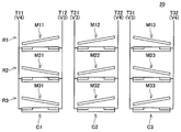
- FIG. 6 is a schematic diagram (part 1) of a matrix portion according to the second embodiment.
- FIG. 10 is a schematic diagram (part 2) of the matrix portion of the second embodiment.
- FIG. 10 is a schematic diagram (part 3) of the matrix portion of the second embodiment.
- FIG. 10 is a schematic diagram (part 4) of the matrix portion of the second embodiment.
- the drive circuit performs a drive method (sequential refresh method) for writing a new swing posture after resetting the stored swing posture to the horizontal state line by line.
- the drive circuit resets the stored swing posture to a horizontal state for all movable units arranged in a matrix, and then writes a new swing posture one row at a time ( Simultaneous refresh method).
- FIG. 1 and 2 show a schematic configuration of the optical deflection apparatus 10 of the present embodiment.
- FIG. 1 is a top view and a block diagram of the optical deflector 10.
- the light deflection apparatus 10 includes a matrix unit 20 and a drive circuit 30.
- the matrix unit 20 is created by a MEMS process
- the drive circuit 30 is created by a CMOS process.
- the matrix unit 20 will be described. As an example, a case where nine movable units M11 to M33 are arranged in a matrix shape of 3 rows ⁇ 3 columns in the matrix unit 20 will be described. Needless to say, the movable units arranged in the matrix unit 20 are not limited to a 3 ⁇ 3 matrix shape but can be expanded to an N ⁇ M (N and M are natural numbers) matrix shape.
- first column C1 three movable units M11, M21, and M31 are arranged in the column direction (y direction) on the same plane. And a pair of 1st electrode T11 and 2nd electrode T12 are connected to movable unit M11, M21, M31 in common.
- the first electrode T11 and the second electrode T12 have a shape extending in parallel in a rail shape in the y direction (column direction).
- movable units M12, M22, and M32 are arranged in the column direction in the second column C2, and are commonly connected by a pair of first electrode T21 and second electrode T22.
- movable units M13, M23, and M33 are arranged in the column direction, and are commonly connected by a pair of first electrode T31 and second electrode T32.
- movable units M11, M12, and M13 are arranged in the row direction (x direction).
- the third electrode T13 is commonly connected to the movable units M11, M12, and M13.
- movable units M21, M22, M23 are arranged in the row direction in the second row R2, and are commonly connected by the third electrode T23.
- movable units M31, M32, and M33 are arranged in the row direction and commonly connected by a third electrode T33.
- the drive circuit 30 includes a CPU 31, a row driver circuit 32, and a column driver circuit 33.
- the CPU 31 is communicably connected to the row driver circuit 32 and the column driver circuit 33.
- the third electrodes T13 to T33 are connected to the row driver circuit 32.
- a bias voltage V1 ( ⁇ 8.5 (V)) or a reset voltage V2 (0 (V)) is applied to the third electrodes T13 to T33 by the row driver circuit 32.
- the column driver circuit 33 includes a first electrode T11 and a second electrode T12 in the first column C1, a first electrode T21 and a second electrode T22 in the second column C2, and a first electrode T31 and a second electrode in the third column C3.
- T32 is connected.
- the column driver circuit 33 causes the first electrode to be moved.
- a proximity voltage V3 (3 (V)) is applied to T11, and a separation voltage V4 (0 (V)) is applied to the second electrode T12.
- the column driver circuit 33 applies the proximity voltage V3 (3 (V)) to the second electrode T12, and the first electrode A separation voltage V4 (0 (V)) is applied to T11.
- the second column C2 and the third column C3, in which the proximity voltage V3 (3 (V)) is applied to the electrode on the end approaching side, and the separation voltage V4 is applied to the electrode on the end separating side. (0 (V)) is applied.
- the bias voltage V1 corresponds to the first voltage
- the reset voltage V2 corresponds to the second voltage
- the proximity voltage V3 corresponds to the third voltage
- the separation voltage V4 corresponds to the fourth voltage.
- FIG. 2 is a top view.
- FIG. 3 is a sectional view taken along line III-III.
- FIG. 4 is a sectional view taken along line IV-IV.
- the movable unit M11 includes a substrate 21, support portions 22a and 22b, movable beams 23a and 23b, a plate-like member 24, a first electrode T11, a second electrode T12, and a third electrode T13.
- the support portions 22a and 22b are fixed to the substrate 21 and extend upward (z direction) from the substrate 21.
- the pair of movable beams 23 a and 23 b connect the upper ends of the pair of support portions 22 a and 22 b and the plate-like member 24.
- the pair of movable beams 23 a and 23 b and the plate-like member 24 are supported at a height away from the substrate 21. Since the pair of movable beams 23a and 23b have low rigidity, they are easy to twist.
- a straight line extending along the movable beams 23a and 23b is defined as a swing axis A1.
- the swing axis A1 has a shape extending in the y direction (column direction).
- the plate-like member 24 has a first end 24a and a second end 24b that face each other with the swing axis A1 interposed therebetween.
- the first electrode T11 is formed on the substrate 21 at a position facing the first end 24a so as to extend in the y direction.
- a third electrode T13 is formed on the lower surface of the plate-like member 24 on the first end 24a side so as to face the first electrode T11.
- the second electrode T12 is formed on the substrate 21 at a position facing the second end 24b so as to extend in the y direction.
- a third electrode T13 is formed on the lower surface of the plate-like member 24 on the second end 24b side so as to face the second electrode T12.
- the pair of movable beams 23 a and 23 b support the plate member 24 so as to be swingable around the swing axis A 1, and exhibit a restoring force for returning the plate member 24 to a posture parallel to the substrate 21. To do.
- a force in the z-axis direction is applied to the first end portion 24a or the second end portion 24b, the movable portion 107 swings with respect to the substrate 21 about the swing axis A1.
- the distance between the first end 24a and the first electrode T11 and the distance between the second end 24b and the second electrode T12 when the plate-like member 24 is in a posture parallel to the substrate 21 are as follows. It is defined as a distance d0. Further, as shown in FIG. 5, the distance between the first end 24a and the first electrode T11 when the first end 24a swings so as to approach the first electrode T11 is defined as a proximity distance d1, The distance between the two end portions 24b and the second electrode T12 is defined as a separation distance d2. 5 is defined as a left-side swinging posture. As shown in FIG. 4, the distance between the first end 24a and the first electrode T11 and the distance between the second end 24b and the second electrode T12 when the plate-like member 24 is in a posture parallel to the substrate 21 are as follows. It is defined as a distance d0. Further, as shown in FIG. 5, the distance between the first end 24a and the first electrode T11 when the first end 24a swings so as to approach the first electrode T11
- the distance between the second end 24b and the second electrode T12 when the second end 24b is swung so as to approach the second electrode T12 is defined as the proximity distance d1
- the distance between the first end 24a and the first electrode T11 is defined as a separation distance d2.
- the posture in FIG. 6 is defined as a right swinging posture.
- the plate-like member 24 has a seesaw structure and swings. And by having a seesaw structure, for example, when the first end 24a is fixed to the first electrode T11, the electrostatic attraction is generated in the second end 24b on the opposite side, thereby eliminating the fixation. Is possible.
- Sequential refresh is a driving method that writes a new swinging posture after resetting the stored swinging posture to a horizontal state one row at a time.
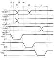
- FIG. 7 shows a timing chart of the voltages VT11 to VT31, the voltages VT12 to VT32, and the voltages VT13 to VT33.
- the voltages VT11 and VT12 are voltages applied to the pair of first electrode T11 and second electrode T12 in the first column C1, and take a value of either 3 (V) or 0 (V).
- the voltages VT21 and VT22 are voltages applied to the pair of first electrode T21 and second electrode T22 in the second column C2, and take a value of 3 (V) or 0 (V). is there.
- the voltages VT31 and VT32 are voltages applied to the pair of first electrode T31 and second electrode T32 in the third column C3, and take a value of either 3 (V) or 0 (V). is there.
- the voltages VT13 to VT33 are voltages applied to the third electrodes T13 to T33 of the first row R1 to the third row R3, and are the bias voltage V1 ( ⁇ 8.5 (V)) or the reset voltage V2 (0 (V )).
- the drive circuit 30 selects the first row R1 to the third row R3 one by one in order. Then, three operations of a reset operation, a swing operation, and a storage operation are performed on the movable unit belonging to the selected row.
- the reset operation is an operation for returning the plate-like member 24 to a parallel state in which the plate member 24 is not swung.
- the swinging operation is an operation of swinging the parallel plate-like members 24 in desired directions. At this time, the plate-like member 24 of the movable unit belonging to the row not selected is maintained in the conventional swinging posture.
- the storing operation is an operation for maintaining the swinging posture of the plate-like member 24 until the next reset operation is performed.
- FIG. 7 the reset operation and the swing operation are performed for the first row R1 in the period P1, the reset operation and the swing operation are performed for the second row R2 in the period P2, and the reset operation is performed for the third row R3 in the period P3. And swinging operation is performed.
- the reset operation and the swing operation of the first row R1 in the period P1 will be described in detail with reference to FIGS. 11 to 15 are schematic views showing the swinging postures of the movable units M11 to M33 in the matrix unit 20.
- FIG. 11 shows the swinging posture of the matrix unit 20 at time t1.
- the swinging posture of FIG. 11 is a state before starting refresh in the first row R1.
- the right swinging posture or the left swinging posture is maintained for all the movable units M11 to M33.
- a reset operation performed at time t2 (FIG. 7) will be described.
- the voltage VT13 applied to the third electrode T13 is changed from the bias voltage V1 ( ⁇ 8.5 (V)) to the reset voltage V2 (0 (V)).
- the reset operation in the movable unit M11 will be described with reference to FIG.
- the electrostatic attractive force between the third electrode T13 and the first electrode T11 at the first end 24a is defined as an electrostatic attractive force F11a
- the third electrode T13 and the second electrode T12 at the second end 24b are defined as Is defined as electrostatic attractive force F11b.
- the resultant force F11 that swings the plate member 24 counterclockwise in FIG. 8 is obtained by the following expression (1).
- the coefficient k is a coefficient determined by the dielectric constant, the electrode area, and the like.
- the reset voltage V2, the proximity voltage V3 and the separation voltage V4, the proximity distance d1, and the separation distance d2 are set so that the torque by the resultant force F11 is smaller than the restoring force of the movable beams 23a and 23b. A relationship has been established.
- the return force of the movable beams 23a and 23b returns the plate-like member 24 to a state where it does not swing, and it is stabilized in a parallel state. Therefore, as shown in FIG. 12, the movable unit M11 returns to the horizontal state.
- the reset operation is similarly performed in the movable units M12 and M13 belonging to the first row R1. Therefore, as shown in FIG. 12, the movable units M12 and M13 also return to the horizontal state.
- the swinging operation performed at time t3 and time t4 (FIG. 7) will be described.
- an operation of swinging the movable unit M11 to the right swinging posture will be described with reference to FIG.
- the plate-like member 24 is in a state parallel to the substrate 21 as shown in FIG.
- the proximity voltage V3 (+3 (V)) is applied to the second electrode T12
- the separation voltage V4 (0 (V)) is applied to the first electrode T11.
- the voltage applied to the third electrode T13 is changed from the reset voltage V2 (0 (V)) to the bias voltage V1 ( ⁇ 8.5 (V)).
- the electrostatic attractive force between the third electrode T13 and the first electrode T11 at the first end 24a is defined as an electrostatic attractive force F12a
- the third electrode T13 and the second electrode T12 at the second end 24b are defined as Is defined as an electrostatic attractive force F12b.
- the resultant force F12 that swings the plate-like member 24 clockwise in FIG. 9 is obtained by the following expression (2).
- the relationship between the bias voltage V1, the proximity voltage V3, the separation voltage V4, and the distance d0 is determined so that the torque by the resultant force F12 exceeds the restoring force of the movable beams 23a and 23b. Therefore, the plate-like member 24 swings to the right side in the drawing so that the second end 24b approaches the second electrode T12. Therefore, as shown in FIG. 13, the movable unit M11 swings to the right side in the drawing.
- the swinging operation is similarly performed in the movable units M12 and M13 belonging to the first row R1. Therefore, as shown in FIG. 13, the movable unit M12 swings to the right in the figure, and the movable unit M13 swings to the left in the figure.
- the movable unit M21 is configured to swing to the left in the drawing at time t3 and time t4, and the bias voltage V1 is applied to the plate member 24 by the third electrode T23.
- the proximity electrostatic attraction FA becomes larger than the separation electrostatic attraction FB, as long as the bias voltage V1 is applied to the third electrode T23, the proximity voltage V3 that reverses the swinging posture and Even if the separation voltage V4 is input to the first electrode T11 and the second electrode T12, the proximity voltage V3 and the separation voltage V4 can be ignored. Therefore, the relationship between the proximity distance d1, the separation distance d2, the bias voltage V1, the proximity voltage V3, and the separation voltage V4 for ignoring the proximity voltage V3 and the separation voltage V4 is obtained by the following equation (5).
- the ratio of the separation distance d2 to the proximity distance d1 ((separation distance d2) / (proximity distance d1)) is defined as the distance ratio DR.
- the ratio of the voltage difference between the bias voltage V1 and the proximity voltage V3 ((V1-V3) / (V1-V4)) to the voltage difference between the bias voltage V1 and the separation voltage V4 is defined as a voltage ratio VR. From equation (5), it can be seen that the magnitude relationship between the electrostatic attraction force FA at the time of proximity and the electrostatic attraction force FB at the time of separation is determined by the magnitude relationship between the distance ratio DR and the voltage ratio VR.
- the relationship among the bias voltage V1, the proximity voltage V3, the separation voltage V4, the proximity distance d1, and the separation distance d2 is determined so that the distance ratio DR is larger than the voltage ratio VR. . That is, in the electrostatic attraction, the relationship between the distance and the voltage is determined so that the end-electrode distance is more dominant than the voltage difference. Then, once the posture of the plate-like member 24 is determined, a voltage that reverses the posture is applied to the first electrode T11 and the second electrode T12 as long as the bias voltage V1 is applied to the third electrode T23. Even if it is done, the swinging posture does not change. That is, the posture of the plate member 24 can be stored by maintaining the state in which the bias voltage V1 is applied to the third electrode T23.
- the conventional swinging posture is maintained in the movable unit M21 in the second row R2.
- the conventional swinging posture is maintained in the movable units M22 and M23 in the second row R2 and M31 to M33 in the third row R3.
- a storage operation performed in a period after time t4 (FIG. 7) will be described.
- the storage operation in the movable unit M11 will be described.
- the storage operation of the movable unit M11 is performed by maintaining the voltage applied to the third electrode T13 at the bias voltage V1 ( ⁇ 8.5 (V)).
- V1 bias voltage
- the right swinging posture is maintained regardless of the voltage applied to the first electrode T11 and the second electrode T12. Since the storing operation is performed based on the above-described principle, detailed description thereof is omitted here. Thereby, the rewriting in the period P1 is completed.
- the bias voltage V1, the proximity voltage V3, the separation voltage V4, the proximity distance d1, and the separation distance d2 are set so that the end-electrode distance is more dominant than the voltage difference. A relationship has been established. Accordingly, the posture of the plate-like member 24 can be stored by maintaining the state in which the bias voltage V1 is applied to the third electrode. Therefore, it is possible to allow a state in which the bias voltage V1 is simultaneously applied to the third electrodes in a plurality of rows.
- the driving speed of the matrix unit 20 is determined by the voltage rise / fall time applied to the third electrode and the response time of the swinging motion of the plate member 24.
- a state in which the bias voltage V1 is simultaneously applied to the third electrodes in a plurality of rows can be allowed. Then, after the voltage applied to the third electrode of a certain row is changed from the bias voltage V1 to the reset voltage V2, the voltage applied to the other third electrode is changed from the reset voltage V2 to the bias voltage V1. Since no time margin is required, the rise / fall time of the voltage applied to the third electrode can be shortened. Therefore, the driving speed of the matrix unit 20 can be increased.
- Example 2 will be described.
- the simultaneous refresh is a driving method for writing a new swinging posture one row at a time after resetting the stored swinging posture to a horizontal state for all the movable units of the matrix unit 20.
- the structures of the matrix unit 20 and the drive circuit 30 are the same as those in the first embodiment, and thus detailed description thereof is omitted here.
- FIG. 16 shows a timing chart of the voltages VT11 to VT31, voltages VT12 to VT32, and voltages VT13 to VT33.
- the drive circuit 30 performs a simultaneous reset operation for the first row R1 to the third row R3. Then, the drive circuit 30 selects the first row R1 to the third row R3 one by one in order, and performs the swing operation and the storage operation for the movable units belonging to the selected row.
- the refresh is performed at time t11
- the swing operation is performed for the first row R1 in the period P11
- the swing operation is performed for the second row R2 in the period P12
- the third row R3 is performed in the period P13.
- a swing motion is performed.
- 17 to 20 are schematic views showing the swinging postures of the movable units M11 to M33 in the matrix unit 20.
- a simultaneous reset operation performed at time t11 (FIG. 16) will be described.
- the voltages VT13 to VT33 are changed from the bias voltage V1 ( ⁇ 8.5 (V)) to the reset voltage V2 (0 (V)). Therefore, as shown in FIG. 17, the postures of all the movable units M11 to M33 are reset to the horizontal state.
- the swinging operation performed at time t12 and time t13 will be described.
- an operation of swinging the movable unit M11 to the left swinging posture will be described.
- the proximity voltage V3 (+3 (V)) is applied to the first electrode T11
- the separation voltage V4 (0 (V)) is applied to the second electrode T12.
- the voltage applied to the third electrode T13 is changed from the reset voltage V2 (0 (V)) to the bias voltage V1 ( ⁇ 8.5 (V)). Therefore, as shown in FIG. 18, the movable unit M11 swings to the left in the drawing.
- the movable unit M12 swings to the left in the drawing, and the movable unit M13 swings to the right in the drawing. Thereby, the swinging operation for the first row R1 in the period P11 is completed.
- the reset voltage V2 is applied to the plate-like members 24 of the movable units M21 and M31.
- the plate-like members 24 of the movable units M21 and M31 are in a posture parallel to the substrate 21, and the distance between the first end 24a and the first electrode T11 and the distance between the second end 24b and the second electrode T12. Are both distance d0.
- the proximity voltage V3 (+3 (V)) is applied to the first electrode T11
- the separation voltage V4 (0 (V)) is applied to the second electrode T12.
- the torque generated when the reset voltage V2 is applied to the plate member 24 is made smaller than the restoring force of the movable beams 23a and 23b.
- the relationship among the reset voltage V2, the proximity voltage V3, the separation voltage V4, and the distance d0 is defined. Therefore, as long as the reset voltage V2 is applied to the plate-like member 24, the plate-like member 24 does not swing and is parallel to the substrate 21 regardless of the voltage applied to the first electrode T11 and the second electrode T12. To maintain.
- the plate-like member 24 does not swing in the movable units M21 and M31 to which the reset voltage V2 is applied. Similarly, the plate-like member 24 does not swing with respect to the movable units M22, M32, M23, and M33. Accordingly, as shown in FIG. 18, the postures of the movable units M21 to M23 in the second row R2 and the movable units M31 to M33 in the third row R3 are maintained in the horizontal state.
- the swinging operation is performed for the second row R2.
- the movable unit belonging to the second row R2 is set to the left swinging posture or the right swinging posture.
- the swinging operation is performed for the third row R3.
- the movable unit belonging to the third row R3 is set to the left swinging posture or the right swinging posture.
- Example 2 will be described. Also in the simultaneous refresh driving method in the second embodiment, it is possible to allow a state in which the bias voltage V1 is simultaneously applied to the third electrodes in a plurality of rows. As a result, it is not necessary to control the timing of applying the bias voltage V1 between the third electrodes of a plurality of rows, so that the control can be simplified and the scale of the drive circuit such as the row driver circuit 32 can be reduced. It becomes. In addition, as a result, the voltage applied to the third electrode in a certain row is changed from the bias voltage V1 to the reset voltage V2, and the voltage applied to the other third electrode is changed from the reset voltage V2 to the bias voltage V1. In addition, since no time margin is required, the rise / fall time of the voltage applied to the third electrode can be shortened.
- the optical deflection apparatus has been described as an example, but the present invention is not limited to this.
- the electrostatic capacitance between the plate-like member 24 and the first electrode T11 and the electrostatic capacitance between the plate-like member 24 and the second electrode T12 it is caused to function as a storage device that recalls the storage state. It is possible. It is also possible to function as a relay device that physically switches the connection destination of the third electrode T13 between the first electrode T11 and the second electrode T12.
- Optical deflection apparatus 20 Matrix part 24 Plate-shaped member 24a 1st end part 24b 2nd end part 30 Drive circuit d0 Distance d1 Proximity distance d2 Separation distance V1 Bias voltage V2 Reset voltage V3 Proximity voltage V4 Isolation voltage M11 thru
Landscapes
- Physics & Mathematics (AREA)
- General Physics & Mathematics (AREA)
- Optics & Photonics (AREA)
- Mechanical Light Control Or Optical Switches (AREA)
- Micromachines (AREA)
Abstract
書込み時間の短縮化や、駆動回路の縮小化が可能な板状部材の揺動装置を提供する。マトリクス部(20)には、可動単位(M11ないしM33)が、マトリクス状に配列される。第1電極(T11ないしT31)及び第2電極(T12ないしT32)は、列方向に並んだ可動単位に共通使用され、行方向に並んだ可動単位の板状部材を共通に接続する第3電極(T13ないしT33)が、行ごとに複数形成されている。駆動回路(30)は、列方向に並んでいる第3電極を順番に1つずつ選択し、選択した第3電極にバイアス電圧を印加すると共に、行方向に複数並んだ第1電極及び第2電極に対して近接電圧または離反電圧を印加することで、板状部材を揺動させる。そして、揺動姿勢を保つ所定期間の間、第3電極に印加される電圧をバイアス電圧に維持し、所定期間の経過後に第3電極に印加される電圧をリセット電圧へ遷移させることで、板状部材を揺動していない状態へ戻す。
Description
本出願は、2009年12月22日に出願された日本国特許出願第2009-291361号に基づく優先権を主張する。その出願の全ての内容はこの明細書中に参照により援用されている。本願は、板状部材を揺動させる装置に関する。
特表2008-515002号公報に開示されている装置では、姿勢を変えることができる板状部材を備えている可動単位の複数個が、行方向と列方向にマトリクス状に配列されている。マトリクス状に配列されている複数個の可動単位を備えているマトリクス型装置を活用するためには、個々の可動単位ごとに他の可動単位から独立して、板状部材の姿勢を切り換えるための駆動装置が必要とされる。特表2008-515002号公報の装置では、行の数だけ独立して存在する行電極と、列の数だけ独立して存在する列電極を利用し、板状部材の姿勢を切り換える行の行電極を選択して+5Vを印加し、他の行の行電極には0Vを印加する。また、その行において、板状部材を基板に接近させる列の列電極には-5Vを印加し、板状部材を基板から離反させる列の列電極には+5Vを印加する。すると、行電極に+5Vが印加されている行では、列電極に-5Vを印加した列の板状部材が基板に接近し、列電極に+5Vを印加した列の板状部材が基板から離反する。その一方において、行電極に0Vが印加されている行では、列電極に-5Vを印加しても+5Vを印加しても、板状部材は姿勢を変えない。この方式によると、任意の交点を選択して板状部材の姿勢を意図した姿勢に切り換えることができるとともに、その操作に伴って他の交点の板状部材の姿勢まで変化することがない。行電極に+5Vを印加する行を順次に切り換えていくことで、マトリクス型装置の全可動単位に対して、個々の可動単位ごとに他の可動単位から独立して、板状部材の姿勢を切り換えることが可能となる。
特表2008-515002号公報のマトリクス型装置では、ある行に対する処理が終了すると、その行に対する新たな処理を禁止してから、次の行への処理を開始する必要がある。例えば、1行目、2行目、3行目の順で板状部材の姿勢を切り換えていく場合、1行目の行電極に+5Vを印加して1行目の処理を完了すると、次に1行目の行電極の電圧を0Vに切り換え、その後に2行目の行電極に+5Vを印加して2行目の処理を実行する。2行目の処理を開始するのに先立って1行目の行電極の電圧を0Vに切り換えておかないと、2行目の処理の際に加える列電極の電圧が1行目に影響してしまい、1行目と2行目を独立に制御することができなくなってしまう。従来の技術では、特定の行に対する処理を終了すると、その行に対するあらたな処理を禁止する状態に切り換えなければならず、その処理に時間を要し、次の行に対する処理開始時間が遅れる。また、あらたな処理を禁止する状態に切り換えてから次の行に対する処理を開始する順序を確実に守る必要があり、あらたな処理を禁止する状態に切り換えてから次の行に対する処理を開始するまでの間に時間マージンが必要となる。これもまた、次の行に対する処理開始時間を遅らせる。
本明細書では、特定の行に対する処理を終了したときに、その行に対するあらたな処理を禁止する状態に切り換えなくても、次の行に対する処理が可能となる技術を開示する。このために、本明細書では、処理を終了した可動単位では、あらたな処理を禁止する状態に切り換えなくても、処理を終了したこと自体によって、あらたな処理が禁止される可動単位を開示する。その性質を備えた可動単位が得られれば、あらたな処理を禁止する状態に切り換える必要がなくなる。その特性を備えた可動単位で1次元のアレイ型装置または2次元のマトリクス型装置を構成すると、あらたな処理を禁止する状態に切り換える必要がないことの利点が顕在化される。本明細書では、単位となる可動単位に有効な技術を開示し、その可動単位の複数個を利用するアレイ型装置とマトリクス型装置に有効な技術を開示する。
本明細書で開示する一つの技術は、新たな処理を禁止する状態に切り換える必要がない可動単位に関する。その装置は、基板と支持部と可動梁と板状部材と第1電極と第2電極と駆動回路を備えている。支持部は、基板に固定されているとともに基板から上方に伸びている。可動梁は、支持部と板状部材を接続しており、板状部材を揺動軸の周りに揺動可能に支持しているともに、板状部材を基板に平行な姿勢に復帰させる復帰力を発揮する。板状部材は、揺動軸を挟んで向かい合う第1端部と第2端部を有しているとともに、少なくとも一部が導電体で形成されている。第1電極は、第1端部と対向する位置の基板上に形成されている。第2電極は、第2端部と対向する位置の基板上に形成されている。駆動回路は、板状部材に第1電圧と第2電圧のうちの一方を印加し、第1電極に第3電圧と第4電圧のうちの一方の電圧を印加するとともに、第2電極に第3電圧と第4電圧のうちの他方の電圧を印加する。第1~第4電圧の制約については後記する。板状部材が基板に平行な姿勢にあるときの第1端部と第1電極の距離と第2端部と第2電極の距離をd0とする。また、板状部材が揺動して第1端部と第1電極の距離が接近したときの近接距離をd1とするとともに第2端部と第2電極の距離が離れたときの離反距離をd2とする。また、板状部材が反対向きに揺動して第2端部と第2電極の距離が接近したときの近接距離をd1とするとともに第1端部と第1電極の距離が離れたときの離反距離をd2とする。このときに、第1電圧ないし第4電圧が以下の(1)ないし(3)の関係を満たしている。
(1)第1端部と第1電極の距離と第2端部と第2電極の距離がd0であり、板状部材に第1電圧を印加し、第1電極に第3電圧と第4電圧のうちの一方の電圧を印加するとともに第2電極に第3電圧と第4電圧のうちの他方の電圧を印加すると、第1電極と第2電極が板状部材に加えるトルクの差が前記復帰力を超える。
(2)板状部材に第2電圧を印加したときに、第1電極と第2電極が板状部材に加えるトルクの差が前記復帰力に満たない。
(3)(第3電圧と第1電圧の電圧差)/(第4電圧と第1電圧の電圧差)の値が、(離反距離d2)/(近接距離d1)の値よりも小さい。
(1)第1端部と第1電極の距離と第2端部と第2電極の距離がd0であり、板状部材に第1電圧を印加し、第1電極に第3電圧と第4電圧のうちの一方の電圧を印加するとともに第2電極に第3電圧と第4電圧のうちの他方の電圧を印加すると、第1電極と第2電極が板状部材に加えるトルクの差が前記復帰力を超える。
(2)板状部材に第2電圧を印加したときに、第1電極と第2電極が板状部材に加えるトルクの差が前記復帰力に満たない。
(3)(第3電圧と第1電圧の電圧差)/(第4電圧と第1電圧の電圧差)の値が、(離反距離d2)/(近接距離d1)の値よりも小さい。
板状部材が第1電極に近づくように揺動すると、第1端部と第1電極の距離が近接距離d1まで近づき、第2端部と第2電極の距離が離反距離d2まで離反する。また、板状部材が第2電極に近づくように揺動すると、第2端部と第2電極の距離が近接距離d1まで近づき、第1端部と第1電極の距離が離反距離d2まで離反する。すなわち、板状部材はシーソー構造を有している。
(1)の関係について説明する。第1電極と板状部材との間に働く静電引力が板状部材を揺動軸の周りに揺動させるトルクとなり、第2電極と板状部材との間に働く静電引力が板状部材を揺動軸の周りに揺動させるトルクとなる。両者のトルクの方向が逆であることから、両者のトルクの差が板状部材を揺動させる有効なトルクとなる。板状部材の端部と電極との間に働く静電引力の大きさは、端部と電極との電圧差の2乗に比例し、端部と電極との距離の2乗に反比例する。板状部材が揺動していない状態では、第1端部と第1電極との間の距離と第2端部と第2電極との間の距離は共にd0となっている。すなわち、端部と電極との距離が離反してしまったとき(d2になったとき)に比して、大きな静電引力が得られる状態になっている。前記(1)の関係は、大きな静電引力が得られる状態で一方の電極に第3電圧を加えて他方の電極に第4電圧を加えると、板状部材に加えられるトルク差が復帰力を上回り、板状部材が可動梁を変形させて揺動することを意味している。すなわち、端部と電極の間の距離がd0であって、離反距離d2である場合よりも大きな静電引力が得られる状態であれば、第3電圧と第4電圧の電圧差が、可動梁の復帰力を上回る有効トルクを生み出すほどに大きいことを意味している。
(2)の関係について説明する。可動単位には、他の可動単位を選択して処理しても処理されず、その可動単位を選択して処理しない限りは処理されない性質が求められる。前記(1)の関係から、処理する可動単位の板状部材に第1電圧を印加すると、その可動単位に対する処理が可能となる。前記(2)の関係にあると、板状部材に第2電圧を印加しておく限り、第1電極と第2電極に印加する電圧と無関係に、第1電極と第2電極が板状部材に加えるトルクの差が可動梁の復帰力に満たないことから、板状部材は揺動せず、基板に平行な姿勢を維持する。すなわち、板状部材に第2電圧を印加しておく限り、他の可動単位の処理のために第1電極と第2電極に電圧を加えても、第2電圧が印加されている可動単位では板状部材が揺動しない。他の可動単位を選択して処理しても処理されず、その可動単位を選択して処理しない限りは処理されない性質が得られる。また可動単位には、処理済の可動単位を処理前の状態に復帰させられる性質が求められる。前記(2)の関係にあると、板状部材に第2電圧を印加すれば、第1電極と第2電極の電圧状態によらないで、板状部材を基板に平行な姿勢に復帰させることが可能となる。前記(1)の関係を利用して板状部材を揺動させるに先立って、板状部材を基板に平行な姿勢に復帰させることが可能となることから、端部と電極の間の距離がd0であって離反距離d2である場合よりも大きな静電引力が得られる状態で、板状部材を揺動させる処理が可能となる。
(3)の関係について説明する。可動単位には、板状部材を揺動させたら、その板状部材を反対方向に揺動させる電圧を第1電極と第2電極に加えても、その揺動姿勢が反転しないことが好ましい。これが可能となれば、ある可動単位の揺動状態を切り換える処理をしてから他の可動単位の揺動状態を切り換える処理に移行する際に、処理済の可動単位に対して新たな処理を禁止する状態に切り換える必要がなくなるからである。 第3電圧が第1電圧と第4電圧よりも大きい場合、前記(1)の関係から、板状部材に第1電圧を印加し、第1電極に第3電圧を印加し、第2電極に第4電圧を印加すると、板状部材は第1電極に接近してその距離がd1となり、板状部材は第2電極から離反してその距離がd2となる。ここで他の可動単位の処理のために第1電極に第3電圧を印加して第2電極に第4電圧を印加する場合、板状部材の揺動方向が反転することはない。それに対して、他の可動単位の処理のために第1電極に第4電圧を印加して第2電極に第3電圧を印加する場合に、板状部材の揺動方向が反転することがあれば、他の可動単位の揺動状態を切り換える前に処理済の可動単位に対して新たな処理を禁止する状態に切り換える必要が生じてしまう。(第3電圧と第1電圧の電圧差)/(第4電圧と第1電圧の電圧差)の値が(離反距離d2)/(近接距離d1)の値よりも小さいと、板状部材と電極の間に働く静電引力の大きさは、板状部材と電極の電圧差の2乗に比例し、板状部材と電極の距離の2乗に反比例する関係にあることから、板状部材と第1電極の距離がd1であり、板状部材と第2電極の距離がd2であれば、板状部材に第1電圧を印加し、第1電極に第4電圧を印加し、第2電極に第3電圧を印加しても、距離と電圧差の関係から、第1電極が板状部材に加えるトルクの方が第2電極が板状部材に加えるトルクよりも大きな関係が維持される。前記(3)の関係にあると、板状部材を揺動させたら、その板状部材を反対方向に揺動させる電圧を第1電極と第2電極に加えても、その揺動姿勢が反転しない性質が得られ、ある可動単位の揺動状態を切り換える処理をしてから他の可動単位の揺動状態を切り換えるまでの間に、処理済の可動単位に対して新たな処理を禁止する状態に切り換える必要がなくなる。
本願の装置では、(1)の関係により、板状部材に第1電圧を印加することによって第1電極と第2電極に印加する電圧によって板状部材を揺動可能な状態とし、(2)の関係により、板状部材に第2電圧を印加することによって第1電極と第2電極に印加する電圧によらないで板状部材を基板に平行な姿勢に戻すかあるいは基板に平行な姿勢に維持することができ、(3)の関係により、板状部材が揺動している可動単位の板状部材に第1電圧を印加し続けた状態で他の可動単位の処理のために第1電極と第2電極に板状部材の揺動方向を反転させる電圧を印加しても、板状部材の揺動方向が反転することがない。処理を終了した可動単位では、あらたな処理を禁止する状態に切り換えなくても、処理を終了したこと自体によって、あらたな処理が禁止される特性を得ることができる。
なお上記装置は、種々のアプリケーションを持つ。例えば、板状部材にミラーを形成することにより、光ビームの反射方向を変化させる光偏向装置を実現することができる。また板状部材と電極間の静電容量を変化させて記憶する記憶装置を実現することができる。また揺動する板状部材によって有接点スイッチを切り換えるリレー装置を実現することもできる。
上記の可動装置は、複数個の可動単位を組み合わせて用いるときに、その特性が有効に活用される。複数個の可動単位を備えている装置は、下記の構成を備えている。可動梁と板状部材と第1電極と第2電極で構成される可動単位の複数個が配置されており、各可動単位の第1電極が共通に駆動回路に接続されており、各可動単位の第2電極が共通に駆動回路に接続されており、各可動単位の板状部材が個別に駆動回路に接続されている。そして第3電圧と第1電圧との電圧差の方が、第4電圧と第1電圧との電圧差よりも大きい関係に調整されている。駆動回路は、板状部材が揺動している可動単位と、板状部材が揺動していない可動単位のうちの一つの可動単位を選択し、選択した可動単位の板状部材に第1電圧を印加し、その他の可動単位の板状部材に第2電圧を印加し、複数個の可動単位の第1電極に共通に第3電圧と第4電圧のうちの一方の電圧を印加するとともに、複数個の可動単位の第2電極に共通に第3電圧と第4電圧のうちの他方の電圧を印加する。すると、複数個の可動単位の中で、次の事象が生じる。
(a)板状部材が揺動していない可動単位のうちの一つであって板状部材に第1電圧が印加された可動単位では、第3電圧が印加された電極に接近する向きに板状部材が揺動し;
(b)板状部材が揺動していない可動単位のうちのその他であって板状部材に第2電圧が印加された可動単位では、板状部材が揺動せず;
(c)板状部材が揺動している可動単位であって板状部材に第1電圧が印加された可動単位では、板状部材が旧来の揺動姿勢を維持する。
駆動回路が、板状部材に第2電圧を印加した可動単位では、板状部材が基板に平行な姿勢に復帰する。
(a)板状部材が揺動していない可動単位のうちの一つであって板状部材に第1電圧が印加された可動単位では、第3電圧が印加された電極に接近する向きに板状部材が揺動し;
(b)板状部材が揺動していない可動単位のうちのその他であって板状部材に第2電圧が印加された可動単位では、板状部材が揺動せず;
(c)板状部材が揺動している可動単位であって板状部材に第1電圧が印加された可動単位では、板状部材が旧来の揺動姿勢を維持する。
駆動回路が、板状部材に第2電圧を印加した可動単位では、板状部材が基板に平行な姿勢に復帰する。
(a)の事象は、板状部材が揺動していない可動単位のうちから、処理対象の可動単位を選択して板状部材を揺動させる。具体的には、板状部材に第1電圧を印加し、第1電極に第3電圧と第4電圧のうちの一方の電圧を印加するとともに、第2電極に第3電圧と第4電圧のうちの他方の電圧を印加する。これにより、第3電圧が印加された電極に接近する向きに板状部材が揺動する。(b)の事象は、板状部材が揺動していない可動単位であって、処理対象外の可動単位の板状部材を揺動させない。具体的には、処理対象外の可動単位の板状部材には第2電圧が印加される。この場合、第1電極に第3電圧と第4電圧のうちの一方の電圧を印加し、第2電極に他方の電圧を印加しても、板状部材に第2電圧が印加されている処理対象外の可動単位の板状部材は揺動しない。(c)の事象は、板状部材が揺動済みの可動単位では揺動姿勢を保持して記憶する。具体的には、第1電圧が板状部材に印加されることで、揺動姿勢が維持される。例えば、板状部材に第1電圧を印加し、第1電極に第3電圧を印加し、第2電極に第4電圧を印加すると、板状部材は第1電極に接近する向きに揺動する。一旦揺動すると、板状部材に第1電圧を印加し続けている限り、その揺動方向が反転することはない。例えば他の可動単位の板状部材を揺動させるために、第1電極に第4電圧を印加し、第2電極に第3電圧を印加しても、第1電極に接近する向きに揺動した板状部材はその姿勢を維持する。さらに、駆動回路が板状部材に第2電圧を印加した可動単位では、板状部材が基板に平行な姿勢に復帰する。これによって、揺動した板状部材を揺動しない姿勢に復帰させることができる。
(a)および(b)の事象を用いることによって、新たに選択された1つの可動単位の板状部材のみを揺動させ、まだ選択していない可動単位の板状部材を揺動させない動作を実現することができる。特定の可動単位を選択して板状部材を揺動させることができる。板状部材を揺動させると元に戻す処理をするまでは揺動した姿勢を維持する。本明細書ででは、板状部材を揺動させることを、処理する、書き込む、あるいは記憶させるということがある。(c)の事象によって、他の可動単位の処理のためにすでに揺動している板状部材の揺動方向を反転させるための電圧を加えても、揺動済の板状部材が反転しないことから、他の可動単位を処理するに先立って、処理済みの可動単位に対する新たな処理を禁止する状態に切り換える必要がない。そして、板状部材に第2電圧を印加することにより、揺動済の板状部材を揺動前の姿勢に戻すことができる。以上によって、複数個の可動単位の第1電極に共通に電圧を印加し、複数個の可動単位の第2電極に共通に電圧を印加しながら、可動単位の一つずつに対して処理することが可能となり、他の可動単位を処理するに先立って処理済みの可動単位に対する新たな処理を禁止する状態に切り換える必要もない。複数個の可動単位で任意のパターンを形成することが可能となる。
本願の装置では、処理済の板状部材に印加する電圧を第1電圧から第2電圧へ切り換えてからでないと、新たな可動単位の板状部材に第1電圧を印加することができないという制約がない。これにより、複数個の可動単位を処理するのに要する時間を短縮することができ、駆動回路を簡単化することが可能となる。
本明細書で開示する技術は、可動単位の複数個が行方向と列方向にマトリクス状に配列されている場合に、特に有用である。この場合は、下記の構成とする。
(1)各々の可動単位が備える揺動軸は列方向に伸びている。
(2)列方向に並んだ可動単位の第1電極が共通に駆動回路に接続されている。
(3)列を異にする可動単位の第1電極が個別に駆動回路に接続されている。
(4)列方向に並んだ可動単位の第2電極が共通に駆動回路に接続されている。
(5)列を異にする可動単位の第2電極が個別に駆動回路に接続されている。
(6)行方向に並んだ可動単位の板状部材が共通に駆動回路に接続されている。
(7)行を異にする可動単位の板状電極が個別に駆動回路に接続されている。
また、駆動回路は、以下の動作を行う。
(A)処理済の行とこれから処理する一つの行を選択し、選択された行に属する可動単位の板状部材に第1電圧を印加するとともに、それ以外の行に属する可動単位の板状部材に第2電圧を印加する。
(B)これから処理する一つの行のうち、第1電極に板状部材を接近させる列では第1電極に第3電圧を印加するとともに第2電極に第4電圧を印加し、第2電極に板状部材を接近させる列では第1電極に第4電圧を印加するとともに第2電極に第3電圧を印加する。
(C)所定時点で板状部材に印加されている電圧を第1電圧から第2電圧に切り換える。
(1)各々の可動単位が備える揺動軸は列方向に伸びている。
(2)列方向に並んだ可動単位の第1電極が共通に駆動回路に接続されている。
(3)列を異にする可動単位の第1電極が個別に駆動回路に接続されている。
(4)列方向に並んだ可動単位の第2電極が共通に駆動回路に接続されている。
(5)列を異にする可動単位の第2電極が個別に駆動回路に接続されている。
(6)行方向に並んだ可動単位の板状部材が共通に駆動回路に接続されている。
(7)行を異にする可動単位の板状電極が個別に駆動回路に接続されている。
また、駆動回路は、以下の動作を行う。
(A)処理済の行とこれから処理する一つの行を選択し、選択された行に属する可動単位の板状部材に第1電圧を印加するとともに、それ以外の行に属する可動単位の板状部材に第2電圧を印加する。
(B)これから処理する一つの行のうち、第1電極に板状部材を接近させる列では第1電極に第3電圧を印加するとともに第2電極に第4電圧を印加し、第2電極に板状部材を接近させる列では第1電極に第4電圧を印加するとともに第2電極に第3電圧を印加する。
(C)所定時点で板状部材に印加されている電圧を第1電圧から第2電圧に切り換える。
上記によると、可動単位を行方向および列方向に配列することで、2次元のマトリクスが形成される。そして、一行ずつ板状部材の姿勢を切り換えることができる(書き込むことができる)。また、処理済みの行に第1電圧を印加し続けることで、書込み状態を記憶することができる。2次元のマトリクスに形成された可動単位で、任意のパターンを形成することができる。処理済の行に印加する電圧を第1電圧から第2電圧に切り換えてからでないと他の行に第1電圧を印加できないという制約がないことから、全部の可動単位に対する処理を完了するまでの時間が短縮化される。
上記において、第2電圧と第4電圧を接地電圧とすることができる。この場合、第2電圧を印加するとは、接地することを意味し、電圧を印加しないことを意味する。同様に、第4電圧を印加するとは、接地することを意味し、電圧を印加しないことを意味する。この場合、第1電圧が正電圧であれば第3電圧を負電圧とし、第1電圧が負電圧であれば第3電圧を正電圧とする。
本技術によれば、書込み時間を短縮することができ、駆動回路を簡単化することが可能となる。
本発明に係る好ましい実施形態は、例えば、下記に列挙する特徴を備えた実施例によって具現化される。
(特徴1)駆動回路は、記憶していた揺動姿勢を1行ずつ水平状態へリセットした上で、新たな揺動姿勢を書き込む駆動方法(逐次リフレッシュ法)を行なう。
(特徴2)駆動回路は、マトリクス状に配列されている全ての可動単位について、記憶していた揺動姿勢を水平状態へリセットした上で、1行ずつ新たな揺動姿勢を書き込む駆動方法(一斉リフレッシュ法)を行なう。
(特徴1)駆動回路は、記憶していた揺動姿勢を1行ずつ水平状態へリセットした上で、新たな揺動姿勢を書き込む駆動方法(逐次リフレッシュ法)を行なう。
(特徴2)駆動回路は、マトリクス状に配列されている全ての可動単位について、記憶していた揺動姿勢を水平状態へリセットした上で、1行ずつ新たな揺動姿勢を書き込む駆動方法(一斉リフレッシュ法)を行なう。
図1および図2に、本実施例の光偏向装置10の概略構成を示す。図1は、光偏向装置10の上面図およびブロック図である。光偏向装置10は、マトリクス部20と、駆動回路30を備えている。マトリクス部20はMEMS工程により作成され、駆動回路30はCMOS工程により作成される。このように、マトリクス部20と駆動回路30とを別工程で形成すことで、歩留まりが低下する事態などを防止することができる。よって、光偏向装置10の作成コストを低減することが可能となる。
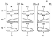
マトリクス部20を説明する。例として、マトリクス部20に、9個の可動単位M11ないしM33が、3行×3列のマトリクス形状に並んでいる場合を説明する。なお、マトリクス部20に配列される可動単位は、3×3のマトリクス形状に限られず、N×M(N、Mは自然数)のマトリクス形状に拡張可能であることは言うまでもない。
第1列C1には、可動単位M11、M21、M31が、同一平面上の列方向(y方向)に3個配列されている。そして、一対の第1電極T11および第2電極T12が、可動単位M11、M21、M31に共通に接続される。第1電極T11および第2電極T12は、y方向(列方向)にレール状に平行に伸びた形状を有する。同様に、第2列C2には可動単位M12、M22、M32が列方向に配列され、一対の第1電極T21および第2電極T22によって共通接続されている。また、第3列C3には可動単位M13、M23、M33が列方向に配列され、一対の第1電極T31および第2電極T32によって共通接続されている。
第1行R1には、可動単位M11、M12、M13が、行方向(x方向)に3個配列されている。そして、第3電極T13が、可動単位M11、M12、M13に共通に接続される。同様に、第2行R2には可動単位M21、M22、M23が行方向に配列され、第3電極T23によって共通接続されている。また、第3行R3には可動単位M31、M32、M33が行方向に配列され、第3電極T33によって共通接続されている。
駆動回路30を説明する。駆動回路30は、CPU31、行ドライバ回路32、列ドライバ回路33を備える。CPU31は、行ドライバ回路32および列ドライバ回路33と通信可能に接続されている。行ドライバ回路32には、第3電極T13ないしT33が接続される。第3電極T13ないしT33には、行ドライバ回路32によって、バイアス電圧V1(-8.5(V))またはリセット電圧V2(0(V))が印加される。列ドライバ回路33には、第1列C1の第1電極T11および第2電極T12、第2列C2の第1電極T21および第2電極T22、第3列C3の第1電極T31および第2電極T32が接続される。第1列C1に属する可動単位M11、M21、M31では、後述するように、第1端部24aを第1電極T11に近づくように揺動させる場合には、列ドライバ回路33によって、第1電極T11に近接電圧V3(3(V))が印加され、第2電極T12に離反電圧V4(0(V))が印加される。一方、第2端部24bを第2電極T12に近づくように揺動させる場合には、列ドライバ回路33によって、第2電極T12に近接電圧V3(3(V))が印加され、第1電極T11に離反電圧V4(0(V))が印加される。第2列C2と第3列C3についても同様であり、端部を接近させる側の電極に近接電圧V3(3(V))が印加され、端部が離反する側の電極には離反電圧V4(0(V))が印加される。なお、バイアス電圧V1が第1電圧に該当し、リセット電圧V2が第2電圧に該当し、近接電圧V3が第3電圧に該当し、離反電圧V4が第4電圧に該当する。
可動単位M11ないしM33の構成を説明する。なお、可動単位M11ないしM33は同一の構造である。よって例として、可動単位M11の構成について、図2ないし図4を用いて説明する。図2は上面図である。図3はIII-III線断面図である。図4はIV-IV線断面図である。可動単位M11は、基板21、支持部22aおよび22b、可動梁23aおよび23b、板状部材24、第1電極T11、第2電極T12、第3電極T13を備えている。支持部22aおよび22bは、基板21に固定されているとともに基板21から上方(z方向)に伸びている。1対の可動梁23aおよび23bは、1対の支持部22aおよび22bの上端と板状部材24とを接続している。1対の可動梁23aおよび23bと板状部材24は、基板21から離反した高さに支持されている。1対の可動梁23aおよび23bは剛性が低くされるため、捩れやすい可動梁とされている。
図2において、可動梁23aおよび23bに沿って伸びる直線を、揺動軸A1と定義する。揺動軸A1は、y方向(列方向)に伸びた形状とされる。板状部材24は、揺動軸A1を挟んで向かい合う第1端部24aと第2端部24bを有している。また図4に示すように、第1電極T11が、第1端部24aと対向する位置の基板21上に、y方向に伸びるように形成されている。そして板状部材24の第1端部24a側の下面には、第1電極T11と対向して、第3電極T13が形成されている。また、第2電極T12が、第2端部24bと対向する位置の基板21上に、y方向に伸びるように形成されている。そして板状部材24の第2端部24b側の下面には、第2電極T12と対向して、第3電極T13が形成されている。
1対の可動梁23aおよび23bは、板状部材24を揺動軸A1の周りに揺動可能に支持しているともに、板状部材24を基板21に平行な姿勢に復帰させる復帰力を発揮するものである。そして、第1端部24aまたは第2端部24bにz軸方向の力を作用させると、可動部107は揺動軸A1を中心として基板21に対して揺動する。
図4ないし図6を用いて、板状部材24の揺動姿勢を説明する。図4に示すように、板状部材24が基板21に平行な姿勢にあるときの第1端部24aと第1電極T11の距離、および第2端部24bと第2電極T12の距離を、距離d0と定義する。また、図5に示すように、第1端部24aが第1電極T11に近づくように揺動した場合における、第1端部24aと第1電極T11の距離を近接距離d1と定義し、第2端部24bと第2電極T12の距離を離反距離d2と定義する。そして、図5の姿勢を左側揺動姿勢と定義する。また、図6に示すように、第2端部24bが第2電極T12に近づくように揺動した場合における、第2端部24bと第2電極T12の距離を近接距離d1と定義し、第1端部24aと第1電極T11の距離を離反距離d2と定義する。そして、図6の姿勢を右側揺動姿勢と定義する。
図5、図6に示すように、板状部材24はシーソー構造を有して揺動する。そして、シーソー構造を有することにより、例えば第1端部24aが第1電極T11に固着した場合には、逆側の第2端部24bに静電引力を発生させることで、固着を解消することが可能とされる。
次に、光偏向装置10の駆動方法について説明する。実施例1では、逐次リフレッシュの駆動方法が行なわれる場合を説明する。逐次リフレッシュは、記憶していた揺動姿勢を1行ずつ水平状態へリセットした上で、新たな揺動姿勢を書き込む駆動方法である。図7に、電圧VT11ないしVT31、電圧VT12ないしVT32、電圧VT13ないしVT33のタイミングチャートを示す。電圧VT11およびVT12は、第1列C1の一対の第1電極T11および第2電極T12に印加される電圧であり、3(V)または0(V)の何れかの値をとる電圧である。また、電圧VT21およびVT22は、第2列C2の一対の第1電極T21および第2電極T22に印加される電圧であり、3(V)または0(V)の何れかの値をとる電圧である。また、電圧VT31およびVT32は、第3列C3の一対の第1電極T31および第2電極T32に印加される電圧であり、3(V)または0(V)の何れかの値をとる電圧である。電圧VT13ないしVT33は、第1行R1から第3行R3の第3電極T13ないしT33に印加される電圧であり、バイアス電圧V1(-8.5(V))またはリセット電圧V2(0(V))の値をとる電圧である。
逐次リフレッシュでは、駆動回路30は、第1行R1ないし第3行R3を順番に1つずつ選択する。そして、選択した行に属する可動単位に対して、リセット動作、揺動動作、記憶動作の3つの動作を行なう。リセット動作は、板状部材24を揺動していない平行状態へ戻す動作である。揺動動作は、平行状態の板状部材24を、それぞれ所望の方向へ揺動させる動作である。このとき、選択していない行に属する可動単位の板状部材24は、旧来の揺動姿勢が維持される。記憶動作は、次のリセット動作が行なわれるまで、板状部材24の揺動姿勢を保つ動作である。
図7において、期間P1では第1行R1についてリセット動作および揺動動作が行なわれ、期間P2では第2行R2についてリセット動作および揺動動作が行なわれ、期間P3では第3行R3についてリセット動作および揺動動作が行なわれる。以下、期間P1での第1行R1のリセット動作および揺動動作について、図8ないし図15を用いて詳細に説明する。なお、図11ないし図15は、マトリクス部20における可動単位M11ないしM33の揺動姿勢を示す模式図である。
図11に、時刻t1におけるマトリクス部20の揺動姿勢を示す。図11の揺動姿勢は、第1行R1にリフレッシュを開始する前の状態である。図11に示すように、全ての可動単位M11ないしM33について、右側揺動姿勢または左側揺動姿勢が維持されている。
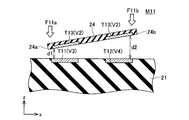
時刻t2(図7)において行なわれる、リセット動作を説明する。時刻t2において、第3電極T13に印加される電圧VT13が、バイアス電圧V1(-8.5(V))からリセット電圧V2(0(V))に変更される。例として、可動単位M11でのリセット動作を、図8を用いて説明する。このとき、第1端部24aの第3電極T13と第1電極T11との間の静電引力を静電引力F11aと定義し、第2端部24bの第3電極T13と第2電極T12との間の静電引力を静電引力F11bと定義する。すると、図8において板状部材24を左回りに揺動させる合力F11は、下式(1)で求められる。
F11=F11a-F11b
=(k×(V2-V3)2/d12 )-(k×(V2-V4)2/d22 )・・・式(1)
ここで係数kは、誘電率や電極面積などによって決まる係数である。そして、本願の可動単位M11では、合力F11によるトルクが可動梁23aおよび23bの復帰力よりも小さくされるように、リセット電圧V2、近接電圧V3および離反電圧V4、近接距離d1、離反距離d2の関係が定められている。よって、可動梁23aおよび23bの復帰力により、板状部材24が揺動していない状態へ戻り、平行状態で安定とされる。よって、図12に示すように、可動単位M11が水平状態へ戻る。なお、第1行R1に属する可動単位M12およびM13においても同様にして、リセット動作が行なわれる。よって、図12に示すように、可動単位M12およびM13も水平状態へ戻る。
F11=F11a-F11b
=(k×(V2-V3)2/d12 )-(k×(V2-V4)2/d22 )・・・式(1)
ここで係数kは、誘電率や電極面積などによって決まる係数である。そして、本願の可動単位M11では、合力F11によるトルクが可動梁23aおよび23bの復帰力よりも小さくされるように、リセット電圧V2、近接電圧V3および離反電圧V4、近接距離d1、離反距離d2の関係が定められている。よって、可動梁23aおよび23bの復帰力により、板状部材24が揺動していない状態へ戻り、平行状態で安定とされる。よって、図12に示すように、可動単位M11が水平状態へ戻る。なお、第1行R1に属する可動単位M12およびM13においても同様にして、リセット動作が行なわれる。よって、図12に示すように、可動単位M12およびM13も水平状態へ戻る。
次に、時刻t3および時刻t4(図7)において行なわれる、揺動動作を説明する。例として、可動単位M11を右側揺動姿勢に揺動する動作を、図9を用いて説明する。時刻t3では、図9に示すように、板状部材24は基板21に平行な状態である。そして、第2電極T12に近接電圧V3(+3(V))を印加するとともに、第1電極T11に離反電圧V4(0(V))を印加する。そして、時刻t4において、第3電極T13に印加される電圧が、リセット電圧V2(0(V))からバイアス電圧V1(-8.5(V))に変更される。このとき、第1端部24aの第3電極T13と第1電極T11との間の静電引力を静電引力F12aと定義し、第2端部24bの第3電極T13と第2電極T12との間の静電引力を静電引力F12bと定義する。すると、図9において板状部材24を右回りに揺動させる合力F12は、下式(2)で求められる。
F12=F12b-F12a
=(k×(V1-V3)2/d02 )-(k×(V1-V4)2/d02 )・・・式(2)
そして、本願の可動単位M11では、合力F12によるトルクが可動梁23aおよび23bの復帰力を超えるように、バイアス電圧V1、近接電圧V3および離反電圧V4、距離d0の関係が定められている。よって、第2端部24bが第2電極T12に近づくように、板状部材24が図中右側へ揺動する。よって、図13に示すように、可動単位M11が図中右側へ揺動する。なお、第1行R1に属する可動単位M12およびM13においても同様にして、揺動動作が行なわれる。よって、図13に示すように、可動単位M12が図中右側へ揺動し、可動単位M13が図中左側へ揺動する。
F12=F12b-F12a
=(k×(V1-V3)2/d02 )-(k×(V1-V4)2/d02 )・・・式(2)
そして、本願の可動単位M11では、合力F12によるトルクが可動梁23aおよび23bの復帰力を超えるように、バイアス電圧V1、近接電圧V3および離反電圧V4、距離d0の関係が定められている。よって、第2端部24bが第2電極T12に近づくように、板状部材24が図中右側へ揺動する。よって、図13に示すように、可動単位M11が図中右側へ揺動する。なお、第1行R1に属する可動単位M12およびM13においても同様にして、揺動動作が行なわれる。よって、図13に示すように、可動単位M12が図中右側へ揺動し、可動単位M13が図中左側へ揺動する。
また、第1行R1の可動単位の揺動動作中における、第2行R2、第3行R3の可動単位の動作を説明する。時刻t3(図7)において、第1電極T11に印加される電圧が近接電圧V3から離反電圧V4へ入れ替えられるとともに、第2電極T12に印加される電圧が離反電圧V4から近接電圧V3へ入れ替えられる。これにより、第1列C1に属する可動単位M11、M21、M31に対して、共通に、右側揺動姿勢をとる旨の命令が伝達されることになる。しかし、後述するように、右側揺動姿勢をとる旨の命令はリフレッシュ済みの可動単位M11のみに有効とされる。そして、リフレッシュされていない可動単位M21およびM31では、右側揺動姿勢をとる旨の命令が無視される。
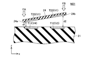
リフレッシュされていない可動単位において、揺動姿勢の命令が無視される原理について説明する。例として、第2行R2に属する可動単位M21での動作を、図10を用いて説明する。可動単位M21は、時刻t3および時刻t4において図中左側へ揺動した姿勢とされており、第3電極T23によってバイアス電圧V1が板状部材24に印加されている。
図10において、第1端部24aについてみると、第1端部24aと第1電極T11が近接距離d1まで近づき、かつ、第3電極T23にバイアス電圧V1(-8.5(V))が印加され、第1電極T11に離反電圧V4(0(V))が印加されている。この場合の静電引力を近接時静電引力FAと定義すると、近接時静電引力FAは下式(3)で求められる。
FA=k×(V1-V4)2/d12 ・・・式(3)
一方、図10において、第2端部24bについてみると、第2端部24bと第2電極T12が離反距離d2まで離れ、かつ、第3電極T23にバイアス電圧V1が印加され、第2電極T12に近接電圧V3(3(V))が印加されている。この場合の静電引力を離反時静電引力FBと定義すると、離反時静電引力FBは下式(4)で求められる。
FB=k×(V1-V3)2/d22 ・・・式(4)
FA=k×(V1-V4)2/d12 ・・・式(3)
一方、図10において、第2端部24bについてみると、第2端部24bと第2電極T12が離反距離d2まで離れ、かつ、第3電極T23にバイアス電圧V1が印加され、第2電極T12に近接電圧V3(3(V))が印加されている。この場合の静電引力を離反時静電引力FBと定義すると、離反時静電引力FBは下式(4)で求められる。
FB=k×(V1-V3)2/d22 ・・・式(4)
そして、近接時静電引力FAが離反時静電引力FBよりも大きくなれば、第3電極T23にバイアス電圧V1を印加している限りは、その揺動姿勢を反転させるような近接電圧V3および離反電圧V4が第1電極T11および第2電極T12に入力されても、当該近接電圧V3および離反電圧V4を無視することができる。よって、近接電圧V3および離反電圧V4を無視するための近接距離d1、離反距離d2、バイアス電圧V1、近接電圧V3、離反電圧V4の関係は、下式(5)により求められる。
FA>FB
k×(V1-V4)2/d12>k×(V1-V3)2/d22
d2/d1>(V1-V3)/(V1-V4)・・・式(5)
FA>FB
k×(V1-V4)2/d12>k×(V1-V3)2/d22
d2/d1>(V1-V3)/(V1-V4)・・・式(5)
ここで、近接距離d1に対する離反距離d2の比率((離反距離d2)/(近接距離d1))を、距離比率DRと定義する。また、バイアス電圧V1と離反電圧V4との電圧差に対する、バイアス電圧V1と近接電圧V3との電圧差の比率((V1-V3)/(V1-V4))を、電圧比率VRと定義する。式(5)より、近接時静電引力FAと離反時静電引力FBとの大小関係は、距離比率DRと電圧比率VRの大小関係で決定されることが分かる。
そして、本願の光偏向装置10では、距離比率DRが電圧比率VRよりも大きくなるように、バイアス電圧V1、近接電圧V3、離反電圧V4、近接距離d1、離反距離d2の関係が定められている。すなわち静電引力において、電圧差よりも端部―電極間距離の方が支配的となるように、距離と電圧との関係が決められている。すると、板状部材24の姿勢が一度決定してしまえば、第3電極T23にバイアス電圧V1を印加している限り、第1電極T11および第2電極T12に姿勢を反転させるような電圧が印加されても、揺動姿勢が変化することがない。すなわち、第3電極T23にバイアス電圧V1を印加した状態を維持することで、板状部材24の姿勢を記憶することができる。
よって、図13の例に示すように、第2行R2の可動単位M21では、旧来の揺動姿勢が維持される。また、第2行R2の可動単位M22およびM23、第3行R3のM31ないしM33においても、同様にして、旧来の揺動姿勢が維持される。
時刻t4以降(図7)の期間において行なわれる、記憶動作について説明する。例として、可動単位M11での記憶動作を説明する。可動単位M11の記憶動作は、第3電極T13に印加される電圧がバイアス電圧V1(-8.5(V))に維持されることで行なわれる。これにより、可動単位M11では、第1電極T11および第2電極T12に印加される電圧に係らず、右側揺動姿勢が維持される。なお、記憶動作は、上述した原理により行なわれるため、ここでは詳細な説明を省略する。これにより、期間P1における書き換えが完了する。
同様にして、期間P2(図7)において、第2行R2について書き換えが行なわれる。そして、図14の例に示すように、第2行R2に属する可動単位のうち、可動単位M22の揺動姿勢のみが左側揺動姿勢から右側揺動姿勢に変更される。また、期間P3において、第3行R3について書き換えが行なわれる。そして、図15の例に示すように、第3行R3に属する可動単位のうち、可動単位M31の揺動姿勢のみが右側揺動姿勢から左側揺動姿勢に変更される。これにより、可動単位M11ないしM33の各々を、ディスプレイデータに対応した姿勢に制御することで、1フレーム分のディスプレイフレームをセットすることができる。そして、所定の周波数でディスプレイフレームを書き換える動作が行なわれることで、プロジェクタ等の画像形成装置に搭載する光偏向装置が実現される。
実施例1に係る光偏向装置10の効果を説明する。実施例1の光偏向装置10では、電圧差よりも端部―電極間距離の方が支配的となるように、バイアス電圧V1、近接電圧V3、離反電圧V4、近接距離d1、離反距離d2の関係が定められている。これにより、第3電極にバイアス電圧V1を印加した状態を維持することで、板状部材24の姿勢を記憶することができる。よって、複数行の第3電極に同時にバイアス電圧V1を印加した状態を許容することができる。すると、ある行の第3電極に印加する電圧をバイアス電圧V1からリセット電圧V2へ遷移してからでないと、他の行の第3電極にバイアス電圧V1を印加することができない、という事態が発生しない。これにより、複数行の第3電極の間でバイアス電圧V1を印加するタイミングを制御する必要がないため、制御を簡略化できる結果、行ドライバ回路32などの駆動回路の規模を縮小することが可能となる。
また、マトリクス部20の駆動速度は、第3電極に印加される電圧の昇降時間と、板状部材24の揺動動作の応答時間で決まる。そして実施例1の光偏向装置10では、複数行の第3電極に同時にバイアス電圧V1を印加した状態を許容することができる。すると、ある行の第3電極に印加される電圧をバイアス電圧V1からリセット電圧V2にしてから、他の第3電極に印加される電圧をリセット電圧V2からバイアス電圧V1にするまでの間に、時間マージンが不要となるため、第3電極に印加される電圧の昇降時間を短くすることができる。よって、マトリクス部20の駆動速度を高めることが出来る。
実施例2を説明する。実施例2では、一斉リフレッシュの駆動方法が行なわれる場合を説明する。一斉リフレッシュは、マトリクス部20の全ての可動単位について、記憶していた揺動姿勢を水平状態へリセットした上で、1行ずつ新たな揺動姿勢を書き込む駆動方法である。なお、マトリクス部20や駆動回路30の構造は実施例1と同様であるため、ここでは詳細な説明は省略する。
図16に、電圧VT11ないしVT31、電圧VT12ないしVT32、電圧VT13ないしVT33のタイミングチャートを示す。一斉リフレッシュでは、駆動回路30は、第1行R1ないし第3行R3について一斉リセット動作を行なう。そして、駆動回路30は、第1行R1ないし第3行R3を順番に1つずつ選択し、選択した行に属する可動単位に対して、揺動動作および記憶動作を行なう。図16において、時刻t11ではリフレッシュが行なわれ、期間P11では第1行R1について揺動動作が行なわれ、期間P12では第2行R2について揺動動作が行なわれ、期間P13では第3行R3について揺動動作が行なわれる。なお、図17ないし図20は、マトリクス部20における可動単位M11ないしM33の揺動姿勢を示す模式図である。
時刻t11(図16)において行なわれる、一斉リセット動作を説明する。時刻t11において、電圧VT13ないしVT33が、バイアス電圧V1(-8.5(V))からリセット電圧V2(0(V))に変更される。よって、図17に示すように、全ての可動単位M11ないしM33の姿勢が、水平状態にリセットされる。
次に、時刻t12および時刻t13において行なわれる、揺動動作を説明する。例として、可動単位M11を左側揺動姿勢に揺動する動作を説明する。時刻t12では、第1電極T11に近接電圧V3(+3(V))が印加されるとともに、第2電極T12に離反電圧V4(0(V))が印加される。そして、時刻t13において、第3電極T13に印加される電圧が、リセット電圧V2(0(V))からバイアス電圧V1(-8.5(V))に変更される。よって、図18に示すように、可動単位M11が図中左側へ揺動する。なお、第1行R1に属する可動単位M12およびM13においても同様にして、可動単位M12が図中左側へ揺動し、可動単位M13が図中右側へ揺動する。これにより、期間P11における第1行R1についての揺動動作が完了する。
また、期間P11における、第2行R2の可動単位M21および第3行R3の可動単位M31の動作を説明する。期間P11では、可動単位M21およびM31の板状部材24にはリセット電圧V2が印加されている。また、可動単位M21およびM31の板状部材24は基板21に平行な姿勢とされており、第1端部24aと第1電極T11の距離、および第2端部24bと第2電極T12の距離は、ともに距離d0とされている。時刻t12において、第1電極T11に近接電圧V3(+3(V))が印加されるとともに、第2電極T12に離反電圧V4(0(V))が印加される。よって、第1列C1に属する可動単位M11、M21、M31に対して、共通に、左側揺動姿勢をとる旨の命令が伝達される。しかし、本願の可動単位M11ないしM33では、前述の通り、リセット電圧V2が板状部材24に印加されているときに発生するトルクが、可動梁23aおよび23bの復帰力よりも小さくされるように、リセット電圧V2、近接電圧V3および離反電圧V4、距離d0の関係が定められている。よって、リセット電圧V2を板状部材24に印加しておく限り、第1電極T11と第2電極T12に印加する電圧と無関係に、板状部材24は揺動せず、基板21に平行な姿勢を維持する。すなわち、可動単位M11の処理のために第1電極T11と第2電極T12に電圧を加えても、リセット電圧V2が印加されている可動単位M21およびM31では板状部材24が揺動しない。なお、可動単位M22、M32、M23、M33についても同様にして、板状部材24が揺動しない。よって、図18に示すように、第2行R2の可動単位M21ないしM23、および第3行R3の可動単位M31ないしM33の姿勢が、水平状態に維持される。
同様にして、期間P12(図16)において、第2行R2について揺動動作が行なわれる。そして、図19の例に示すように、第2行R2に属する可動単位が左側揺動姿勢または右側揺動姿勢に設定される。また、期間P13において、第3行R3について揺動動作が行なわれる。そして、図20の例に示すように、第3行R3に属する可動単位が左側揺動姿勢または右側揺動姿勢に設定される。
実施例2の効果を説明する。実施例2における一斉リフレッシュの駆動方法においても、複数行の第3電極に同時にバイアス電圧V1を印加した状態を許容することができる。これにより、複数行の第3電極の間でバイアス電圧V1を印加するタイミングを制御する必要がないため、制御を簡略化できる結果、行ドライバ回路32などの駆動回路の規模を縮小することが可能となる。またこれにより、ある行の第3電極に印加される電圧をバイアス電圧V1からリセット電圧V2にしてから、他の第3電極に印加される電圧をリセット電圧V2からバイアス電圧V1にするまでの間に、時間マージンが不要となるため、第3電極に印加される電圧の昇降時間を短くすることができる。
以上、本願の実施例について詳細に説明したが、これらは例示に過ぎず、特許請求の範囲を限定するものではない。特許請求の範囲に記載の技術には、以上に例示した具体例を様々に変形、変更したものが含まれる。
本願では、光偏向装置を例として説明したが、この形態に限られない。例えば、板状部材24と第1電極T11の間の静電容量や、板状部材24と第2電極T12との間の静電容量を検知することで、記憶状態を呼び出す記憶装置として機能させることが可能である。また、第3電極T13の接続先を、第1電極T11と第2電極T12との間で物理的に切り替えるリレー装置として機能させることも可能である。
本明細書または図面に説明した技術要素は、単独であるいは各種の組合せによって技術的有用性を発揮するものであり、出願時請求項記載の組合せに限定されるものではない。また、本明細書または図面に例示した技術は複数目的を同時に達成し得るものであり、そのうちの一つの目的を達成すること自体で技術的有用性を持つものである。
10 光偏向装置
20 マトリクス部
24 板状部材
24a 第1端部
24b 第2端部
30 駆動回路
d0 距離
d1 近接距離
d2 離反距離
V1 バイアス電圧
V2 リセット電圧
V3 近接電圧
V4 離反電圧
M11ないしM33 可動単位
T11ないしT31 第1電極
T12ないしT32 第2電極
T13ないしT33 第3電極
20 マトリクス部
24 板状部材
24a 第1端部
24b 第2端部
30 駆動回路
d0 距離
d1 近接距離
d2 離反距離
V1 バイアス電圧
V2 リセット電圧
V3 近接電圧
V4 離反電圧
M11ないしM33 可動単位
T11ないしT31 第1電極
T12ないしT32 第2電極
T13ないしT33 第3電極
Claims (4)
- 基板と支持部と可動梁と板状部材と第1電極と第2電極と駆動回路を備えており、
支持部は、基板に固定されているとともに基板から上方に伸びており、
可動梁は、支持部と板状部材を接続しており、板状部材を揺動軸の周りに揺動可能に支持しているともに、板状部材を基板に平行な姿勢に復帰させる復帰力を発揮し、
板状部材は、揺動軸を挟んで向かい合う第1端部と第2端部を有しているとともに、少なくとも一部が導電体で形成されており、
第1電極は、第1端部と対向する位置の基板上に形成されており、
第2電極は、第2端部と対向する位置の基板上に形成されており、
駆動回路は、板状部材に第1電圧と第2電圧のうちの一方を印加し、第1電極に第3電圧と第4電圧のうちの一方の電圧を印加するとともに、第2電極に第3電圧と第4電圧のうちの他方の電圧を印加し、
板状部材が基板に平行な姿勢にあるときの第1端部と第1電極の距離と第2端部と第2電極の距離をd0とし、板状部材が揺動して第1端部と第1電極の距離が接近したときの近接距離をd1とするとともに第2端部と第2電極の距離が離れたときの離反距離をd2とし、板状部材が反対向きに揺動して第2端部と第2電極の距離が接近したときの近接距離をd1とするとともに第1端部と第1電極の距離が離れたときの離反距離をd2としたときに、第1電圧ないし第4電圧が以下の(1)ないし(3)の関係を満たしており、板状部材の揺動状態を制御可能な装置:
(1)第1端部と第1電極の距離と第2端部と第2電極の距離がd0であり、板状部材に第1電圧を印加し、第1電極に第3電圧と第4電圧のうちの一方の電圧を印加するとともに、第2電極に第3電圧と第4電圧のうちの他方の電圧を印加するときに、第1電極と第2電極が板状部材に加えるトルクの差が前記復帰力を超え;
(2)板状部材に第2電圧を印加したときに、第1電極と第2電極が板状部材に加えるトルクの差が前記復帰力に満たず;
(3)(第3電圧と第1電圧の電圧差)/(第4電圧と第1電圧の電圧差)の値が、(離反距離d2)/(近接距離d1)の値よりも小さい。 - 請求項1に記載の可動梁と板状部材と第1電極と第2電極で構成される可動単位の複数個を備えており、
各可動単位の第1電極が共通に駆動回路に接続されており、
各可動単位の第2電極が共通に駆動回路に接続されており、
各可動単位の板状部材が個別に駆動回路に接続されており、
第3電圧と第1電圧との電圧差の方が、第4電圧と第1電圧との電圧差より大きく、
駆動回路が、板状部材が揺動している可動単位と、板状部材が揺動していない可動単位のうちの一つの可動単位を選択し、選択した可動単位の板状部材に第1電圧を印加し、その他の可動単位の板状部材に第2電圧を印加し、複数個の可動単位の第1電極に共通に第3電圧と第4電圧のうちの一方の電圧を印加するとともに、複数個の可動単位の第2電極に共通に第3電圧と第4電圧のうちの他方の電圧を印加したときに、複数個の可動単位の中で、次の事象が生じて板状部材の揺動状態を制御可能な装置:
(a)板状部材が揺動していない可動単位のうちの一つであって板状部材に第1電圧が印加された可動単位では、第3電圧が印加された電極に接近する向きに板状部材が揺動し;
(b)板状部材が揺動していない可動単位のうちのその他であって板状部材に第2電圧が印加された可動単位では、板状部材が揺動せず;
(c)板状部材が揺動している可動単位であって板状部材に第1電圧が印加された可動単位では、板状部材が旧来の揺動姿勢を維持し、
駆動回路が、板状部材に第2電圧を印加した可動単位では、板状部材が基板に平行な姿勢に復帰する。 - 請求項2に記載の可動単位の複数個が行方向と列方向にマトリクス状に配列され、
各々の可動単位が備える前記揺動軸は列方向に伸びた形状とされ、
列方向に並んだ可動単位の第1電極が共通に駆動回路に接続されているとともに、列を異にする可動単位の第1電極が個別に駆動回路に接続されており、
列方向に並んだ可動単位の第2電極が共通に駆動回路に接続されているとともに、列を異にする可動単位の第2電極が個別に駆動回路に接続されており、
行方向に並んだ可動単位の板状部材が共通に駆動回路に接続されているとともに、行を異にする可動単位の板状電極が個別に駆動回路に接続されており、
前記駆動回路は、
(A)処理済の行とこれから処理する一つの行を選択し、選択された行に属する可動単位の板状部材に第1電圧を印加するとともに、それ以外の行に属する可動単位の板状部材に第2電圧を印加し、
(B)これから処理する一つの行のうち、第1電極に板状部材を接近させる列では第1電極に第3電圧を印加するとともに第2電極に第4電圧を印加し、第2電極に板状部材を接近させる列では第1電極に第4電圧を印加するとともに第2電極に第3電圧を印加し、
(C)所定時点で板状部材に印加されている電圧を第1電圧から第2電圧に切り換える
ことを特徴とする板状部材の揺動状態を制御可能な装置。 - 第2電圧と第4電圧は接地電圧であり、第1電圧が正電圧であれば第3電圧が負電圧であり、第1電圧が負電圧であれば第3電圧が正電圧であることを特徴とする請求項1から3のいずれかに記載の装置。
Priority Applications (1)
| Application Number | Priority Date | Filing Date | Title |
|---|---|---|---|
| US13/394,699 US9075234B2 (en) | 2009-12-22 | 2010-12-14 | Tabular member swinging device |
Applications Claiming Priority (2)
| Application Number | Priority Date | Filing Date | Title |
|---|---|---|---|
| JP2009291361A JP5310529B2 (ja) | 2009-12-22 | 2009-12-22 | 板状部材の揺動装置 |
| JP2009-291361 | 2009-12-22 |
Publications (1)
| Publication Number | Publication Date |
|---|---|
| WO2011078015A1 true WO2011078015A1 (ja) | 2011-06-30 |
Family
ID=44195544
Family Applications (1)
| Application Number | Title | Priority Date | Filing Date |
|---|---|---|---|
| PCT/JP2010/072482 Ceased WO2011078015A1 (ja) | 2009-12-22 | 2010-12-14 | 板状部材の揺動装置 |
Country Status (3)
| Country | Link |
|---|---|
| US (1) | US9075234B2 (ja) |
| JP (1) | JP5310529B2 (ja) |
| WO (1) | WO2011078015A1 (ja) |
Cited By (1)
| Publication number | Priority date | Publication date | Assignee | Title |
|---|---|---|---|---|
| CN108269532A (zh) * | 2018-01-19 | 2018-07-10 | 友达光电股份有限公司 | 显示装置 |
Citations (1)
| Publication number | Priority date | Publication date | Assignee | Title |
|---|---|---|---|---|
| JP2004101553A (ja) * | 2002-09-04 | 2004-04-02 | Seiko Epson Corp | ミラーデバイス、光スイッチ、電子機器およびミラーデバイス駆動方法 |
Family Cites Families (52)
| Publication number | Priority date | Publication date | Assignee | Title |
|---|---|---|---|---|
| US7471444B2 (en) * | 1996-12-19 | 2008-12-30 | Idc, Llc | Interferometric modulation of radiation |
| WO2003007049A1 (en) * | 1999-10-05 | 2003-01-23 | Iridigm Display Corporation | Photonic mems and structures |
| US6552840B2 (en) * | 1999-12-03 | 2003-04-22 | Texas Instruments Incorporated | Electrostatic efficiency of micromechanical devices |
| US6504641B2 (en) * | 2000-12-01 | 2003-01-07 | Agere Systems Inc. | Driver and method of operating a micro-electromechanical system device |
| US7142346B2 (en) * | 2003-12-09 | 2006-11-28 | Idc, Llc | System and method for addressing a MEMS display |
| US7889163B2 (en) * | 2004-08-27 | 2011-02-15 | Qualcomm Mems Technologies, Inc. | Drive method for MEMS devices |
| US7560299B2 (en) * | 2004-08-27 | 2009-07-14 | Idc, Llc | Systems and methods of actuating MEMS display elements |
| US7515147B2 (en) * | 2004-08-27 | 2009-04-07 | Idc, Llc | Staggered column drive circuit systems and methods |
| US7499208B2 (en) * | 2004-08-27 | 2009-03-03 | Udc, Llc | Current mode display driver circuit realization feature |
| US7551159B2 (en) * | 2004-08-27 | 2009-06-23 | Idc, Llc | System and method of sensing actuation and release voltages of an interferometric modulator |
| US7602375B2 (en) * | 2004-09-27 | 2009-10-13 | Idc, Llc | Method and system for writing data to MEMS display elements |
| US7359066B2 (en) * | 2004-09-27 | 2008-04-15 | Idc, Llc | Electro-optical measurement of hysteresis in interferometric modulators |
| US7453579B2 (en) * | 2004-09-27 | 2008-11-18 | Idc, Llc | Measurement of the dynamic characteristics of interferometric modulators |
| US7327510B2 (en) * | 2004-09-27 | 2008-02-05 | Idc, Llc | Process for modifying offset voltage characteristics of an interferometric modulator |
| US7545550B2 (en) * | 2004-09-27 | 2009-06-09 | Idc, Llc | Systems and methods of actuating MEMS display elements |
| US8878825B2 (en) * | 2004-09-27 | 2014-11-04 | Qualcomm Mems Technologies, Inc. | System and method for providing a variable refresh rate of an interferometric modulator display |
| CN100439967C (zh) * | 2004-09-27 | 2008-12-03 | Idc公司 | 用于多状态干涉光调制的方法和设备 |
| US7302157B2 (en) * | 2004-09-27 | 2007-11-27 | Idc, Llc | System and method for multi-level brightness in interferometric modulation |
| US8514169B2 (en) * | 2004-09-27 | 2013-08-20 | Qualcomm Mems Technologies, Inc. | Apparatus and system for writing data to electromechanical display elements |
| US7551246B2 (en) * | 2004-09-27 | 2009-06-23 | Idc, Llc. | System and method for display device with integrated desiccant |
| US7345805B2 (en) * | 2004-09-27 | 2008-03-18 | Idc, Llc | Interferometric modulator array with integrated MEMS electrical switches |
| US20060066594A1 (en) * | 2004-09-27 | 2006-03-30 | Karen Tyger | Systems and methods for driving a bi-stable display element |
| US7289256B2 (en) * | 2004-09-27 | 2007-10-30 | Idc, Llc | Electrical characterization of interferometric modulators |
| US7136213B2 (en) * | 2004-09-27 | 2006-11-14 | Idc, Llc | Interferometric modulators having charge persistence |
| US7701631B2 (en) * | 2004-09-27 | 2010-04-20 | Qualcomm Mems Technologies, Inc. | Device having patterned spacers for backplates and method of making the same |
| US7573547B2 (en) * | 2004-09-27 | 2009-08-11 | Idc, Llc | System and method for protecting micro-structure of display array using spacers in gap within display device |
| US7532195B2 (en) * | 2004-09-27 | 2009-05-12 | Idc, Llc | Method and system for reducing power consumption in a display |
| US8310441B2 (en) * | 2004-09-27 | 2012-11-13 | Qualcomm Mems Technologies, Inc. | Method and system for writing data to MEMS display elements |
| US7675669B2 (en) | 2004-09-27 | 2010-03-09 | Qualcomm Mems Technologies, Inc. | Method and system for driving interferometric modulators |
| US7626581B2 (en) * | 2004-09-27 | 2009-12-01 | Idc, Llc | Device and method for display memory using manipulation of mechanical response |
| US7679627B2 (en) * | 2004-09-27 | 2010-03-16 | Qualcomm Mems Technologies, Inc. | Controller and driver features for bi-stable display |
| US7446927B2 (en) * | 2004-09-27 | 2008-11-04 | Idc, Llc | MEMS switch with set and latch electrodes |
| US7724993B2 (en) * | 2004-09-27 | 2010-05-25 | Qualcomm Mems Technologies, Inc. | MEMS switches with deforming membranes |
| US7843410B2 (en) * | 2004-09-27 | 2010-11-30 | Qualcomm Mems Technologies, Inc. | Method and device for electrically programmable display |
| US7310179B2 (en) * | 2004-09-27 | 2007-12-18 | Idc, Llc | Method and device for selective adjustment of hysteresis window |
| US7920136B2 (en) * | 2005-05-05 | 2011-04-05 | Qualcomm Mems Technologies, Inc. | System and method of driving a MEMS display device |
| US7948457B2 (en) * | 2005-05-05 | 2011-05-24 | Qualcomm Mems Technologies, Inc. | Systems and methods of actuating MEMS display elements |
| JP2006346817A (ja) * | 2005-06-16 | 2006-12-28 | Fujifilm Holdings Corp | 微小電気機械素子アレイ装置及びその駆動方法 |
| JP2007015067A (ja) * | 2005-07-08 | 2007-01-25 | Fujifilm Holdings Corp | 微小薄膜可動素子及び微小薄膜可動素子アレイ並びに画像形成装置 |
| JP2007033787A (ja) * | 2005-07-26 | 2007-02-08 | Fujifilm Corp | 微小薄膜可動素子および微小薄膜可動素子アレイ並びに微小薄膜可動素子アレイの駆動方法 |
| JP4810154B2 (ja) * | 2005-07-28 | 2011-11-09 | 富士フイルム株式会社 | 微小電気機械素子の駆動方法、微小電気機械素子アレイ及び画像形成装置 |
| US7355779B2 (en) | 2005-09-02 | 2008-04-08 | Idc, Llc | Method and system for driving MEMS display elements |
| US20070126673A1 (en) * | 2005-12-07 | 2007-06-07 | Kostadin Djordjev | Method and system for writing data to MEMS display elements |
| US8391630B2 (en) * | 2005-12-22 | 2013-03-05 | Qualcomm Mems Technologies, Inc. | System and method for power reduction when decompressing video streams for interferometric modulator displays |
| JP2007199101A (ja) * | 2006-01-23 | 2007-08-09 | Fujifilm Corp | 微小電気機械素子アレイ装置及び画像形成装置 |
| US8194056B2 (en) * | 2006-02-09 | 2012-06-05 | Qualcomm Mems Technologies Inc. | Method and system for writing data to MEMS display elements |
| JP4966562B2 (ja) * | 2006-02-28 | 2012-07-04 | 富士フイルム株式会社 | 微小電気機械式素子、微小電気機械式素子アレイ、光変調素子、微小電気機械式光変調素子、微小電気機械式光変調素子アレイ、及びこれらを用いた画像形成装置 |
| JP4792322B2 (ja) * | 2006-04-04 | 2011-10-12 | 富士フイルム株式会社 | 微小電気機械式変調素子、微小電気機械式変調素子アレイ、画像形成装置、及び微小電気機械式変調素子の設計方法 |
| US7443568B2 (en) * | 2006-05-04 | 2008-10-28 | Miradia Inc. | Method and system for resonant operation of a reflective spatial light modulator |
| US7505195B2 (en) * | 2006-05-04 | 2009-03-17 | Miradia Inc. | Reflective spatial light modulator with high stiffness torsion spring hinge |
| US7863799B1 (en) * | 2007-03-02 | 2011-01-04 | AG Microsystems Inc. | Micro electro mechanical system using comb and parallel plate actuation |
| US8884940B2 (en) * | 2010-01-06 | 2014-11-11 | Qualcomm Mems Technologies, Inc. | Charge pump for producing display driver output |
-
2009
- 2009-12-22 JP JP2009291361A patent/JP5310529B2/ja not_active Expired - Fee Related
-
2010
- 2010-12-14 WO PCT/JP2010/072482 patent/WO2011078015A1/ja not_active Ceased
- 2010-12-14 US US13/394,699 patent/US9075234B2/en not_active Expired - Fee Related
Patent Citations (1)
| Publication number | Priority date | Publication date | Assignee | Title |
|---|---|---|---|---|
| JP2004101553A (ja) * | 2002-09-04 | 2004-04-02 | Seiko Epson Corp | ミラーデバイス、光スイッチ、電子機器およびミラーデバイス駆動方法 |
Cited By (1)
| Publication number | Priority date | Publication date | Assignee | Title |
|---|---|---|---|---|
| CN108269532A (zh) * | 2018-01-19 | 2018-07-10 | 友达光电股份有限公司 | 显示装置 |
Also Published As
| Publication number | Publication date |
|---|---|
| US20120169702A1 (en) | 2012-07-05 |
| US9075234B2 (en) | 2015-07-07 |
| JP2011131302A (ja) | 2011-07-07 |
| JP5310529B2 (ja) | 2013-10-09 |
Similar Documents
| Publication | Publication Date | Title |
|---|---|---|
| JP3543303B2 (ja) | マルチフォールデッドスプリングを用いた多軸駆動のためのシングルステージマイクロアクチュエータ | |
| JP2002341267A (ja) | 光学多層構造体の駆動方法および表示装置の駆動方法ならびに表示装置 | |
| US20070158552A1 (en) | Two-axis micro optical scanner | |
| CN102067009A (zh) | 活动结构及使用该活动结构的微镜器件 | |
| JP2003209981A (ja) | 圧電アクチュエータ及びそれを備えた電子機器 | |
| US20200209614A1 (en) | Mems electrostatic actuator with linearized displacements | |
| KR101838101B1 (ko) | 변형 거울 구동 장치 | |
| JPH10197819A (ja) | 光スキャナ | |
| US11016288B2 (en) | Adaptable displays using piezoelectric actuators | |
| JP6568591B2 (ja) | Memsアクチュエータ、複数のmemsアクチュエータを備えるシステム、およびmemsアクチュエータを製造する方法 | |
| JP5310529B2 (ja) | 板状部材の揺動装置 | |
| US7294950B2 (en) | Electrostatic actuator, electrostatic actuator driving method electromechanical transducer, and electromechanical transducer driving method | |
| KR20050020381A (ko) | 대면적 스테이지를 구비한 2축 액츄에이터 | |
| JP4743630B2 (ja) | 光偏向装置、光偏向装置アレイおよび画像投影表示装置 | |
| JP2006115683A (ja) | 静電アクチュエータ及び光走査装置 | |
| JP2010008614A (ja) | 投影型表示装置及びそれに用いられる表示方法 | |
| JP2007312553A (ja) | マイクロアクチュエータ、光学デバイス及び表示装置 | |
| JP2007017769A (ja) | 光通信用微小薄膜可動素子及び微小薄膜可動素子アレイ | |
| JPH1195252A (ja) | 表示装置 | |
| JP2007199101A (ja) | 微小電気機械素子アレイ装置及び画像形成装置 | |
| CN117198221B (zh) | 一种数据存储电路、硅基显示面板及显示装置 | |
| CN115561895B (zh) | 一种狭长形的压电mems微镜 | |
| EP4080268B1 (en) | Piezoelectric based mems device with time sharing actuation and sensing circuitry | |
| CN117930494A (zh) | 一种微镜装置 | |
| KR20120107002A (ko) | 디스플레이 라인 업데이트 순서 변경 |
Legal Events
| Date | Code | Title | Description |
|---|---|---|---|
| 121 | Ep: the epo has been informed by wipo that ep was designated in this application |
Ref document number: 10839248 Country of ref document: EP Kind code of ref document: A1 |
|
| WWE | Wipo information: entry into national phase |
Ref document number: 13394699 Country of ref document: US |
|
| NENP | Non-entry into the national phase |
Ref country code: DE |
|
| 122 | Ep: pct application non-entry in european phase |
Ref document number: 10839248 Country of ref document: EP Kind code of ref document: A1 |