WO2011074684A1 - 基板およびそれを用いた回路装置の製造方法 - Google Patents
基板およびそれを用いた回路装置の製造方法 Download PDFInfo
- Publication number
- WO2011074684A1 WO2011074684A1 PCT/JP2010/072826 JP2010072826W WO2011074684A1 WO 2011074684 A1 WO2011074684 A1 WO 2011074684A1 JP 2010072826 W JP2010072826 W JP 2010072826W WO 2011074684 A1 WO2011074684 A1 WO 2011074684A1
- Authority
- WO
- WIPO (PCT)
- Prior art keywords
- substrate
- mounting
- mounting substrate
- circuit device
- slit
- Prior art date
- Legal status (The legal status is an assumption and is not a legal conclusion. Google has not performed a legal analysis and makes no representation as to the accuracy of the status listed.)
- Ceased
Links
Images



Classifications
-
- H—ELECTRICITY
- H05—ELECTRIC TECHNIQUES NOT OTHERWISE PROVIDED FOR
- H05K—PRINTED CIRCUITS; CASINGS OR CONSTRUCTIONAL DETAILS OF ELECTRIC APPARATUS; MANUFACTURE OF ASSEMBLAGES OF ELECTRICAL COMPONENTS
- H05K3/00—Apparatus or processes for manufacturing printed circuits
- H05K3/0011—Working of insulating substrates or insulating layers
- H05K3/0044—Mechanical working of the substrate, e.g. drilling or punching
- H05K3/0052—Depaneling, i.e. dividing a panel into circuit boards; Working of the edges of circuit boards
-
- H—ELECTRICITY
- H05—ELECTRIC TECHNIQUES NOT OTHERWISE PROVIDED FOR
- H05K—PRINTED CIRCUITS; CASINGS OR CONSTRUCTIONAL DETAILS OF ELECTRIC APPARATUS; MANUFACTURE OF ASSEMBLAGES OF ELECTRICAL COMPONENTS
- H05K2201/00—Indexing scheme relating to printed circuits covered by H05K1/00
- H05K2201/09—Shape and layout
- H05K2201/09009—Substrate related
- H05K2201/09063—Holes or slots in insulating substrate not used for electrical connections
-
- H—ELECTRICITY
- H05—ELECTRIC TECHNIQUES NOT OTHERWISE PROVIDED FOR
- H05K—PRINTED CIRCUITS; CASINGS OR CONSTRUCTIONAL DETAILS OF ELECTRIC APPARATUS; MANUFACTURE OF ASSEMBLAGES OF ELECTRICAL COMPONENTS
- H05K2201/00—Indexing scheme relating to printed circuits covered by H05K1/00
- H05K2201/09—Shape and layout
- H05K2201/09009—Substrate related
- H05K2201/0909—Preformed cutting or breaking line
-
- H—ELECTRICITY
- H10—SEMICONDUCTOR DEVICES; ELECTRIC SOLID-STATE DEVICES NOT OTHERWISE PROVIDED FOR
- H10W—GENERIC PACKAGES, INTERCONNECTIONS, CONNECTORS OR OTHER CONSTRUCTIONAL DETAILS OF DEVICES COVERED BY CLASS H10
- H10W72/00—Interconnections or connectors in packages
- H10W72/851—Dispositions of multiple connectors or interconnections
- H10W72/874—On different surfaces
- H10W72/884—Die-attach connectors and bond wires
Definitions
- the present invention relates to a substrate and a method of manufacturing a circuit device using the substrate.
- the present invention relates to a substrate on which a plurality of mounting substrates elongated in one direction are connected, and a method of manufacturing a circuit device using the substrate.
- the substrate 100 is a substrate made of metal such as aluminum and having a thickness of about 1.5 mm, and as a specific example, the width in the depth direction on the paper is about 20 cm, and the length in the lateral direction is It is about 70 cm.
- a large number of mounting substrates 106 are provided inside the substrate 100 of such a size.
- the size of one mounting substrate 106 is about 60 cm in the lateral direction and about 0.6 cm in width L10. That is, the mounting substrate 106 is a substrate formed to be extremely elongated in the lateral direction.
- the mounting substrate 106 of such a shape is specified as a substrate of a backlight incorporated in a monitor such as an LCD.
- slits 120 are provided between the respective mounting substrates 106 by partially punching out and removing the substrate 100.
- the lateral length of the slit 120 is the same as that of the mounting substrate 106, and the width L11 is about 2 mm. That is, the left and right end portions of each mounting substrate 106 are connected to the frame-like support portion of the substrate 100, thereby maintaining the integrated substrate state as a whole.
- FIGS. 7B and 7C A method of manufacturing a circuit device using the substrate 100 configured as described above will be described with reference to FIGS. 7B and 7C.
- the upper surface of each mounting substrate 106 made of metal is covered with an insulating layer 102 made of resin. Furthermore, a conductive pattern 104 having a predetermined shape is formed on the upper surface of the insulating layer 102.
- the circuit element 112 is mounted on the conductive pattern 104 of each mounting substrate 106.
- another element such as an LED which is a light emitting element or a transistor is adopted.
- FIG. 7A the left and right end portions of each mounting substrate 106 are cut from the frame-shaped support portion of the substrate 100. Cutting of each mounting substrate 106 is performed by pressing or dicing.
- each mounting substrate 106 is bent in the middle of the manufacturing process.
- the mounting substrate 106 provided on the large-sized substrate 100 has a very elongated shape in the lateral direction.
- the mounting substrate 106 is only supported at its both ends by the frame-like support portion of the substrate 100, and the middle portion in the longitudinal direction is not mechanically supported. Therefore, if the end of the substrate 100 is held and transported in the middle of the manufacturing process, each mounting substrate 106 is bent by its own weight, and the bending destroys the conductive pattern and the circuit element formed on the upper surface.
- the mounting substrate 106 itself may be deformed. Furthermore, considering that the width L11 of the slit 120 provided by removing the substrate 100 by punching is about 0.2 cm and the width L10 of the mounting substrate 120 is 0.6 cm, it is about 1/3 of the substrate 100. Are removed for the slit 120 and discarded. Furthermore, it was difficult to form the slit 120 having a width L11 narrower than 0.2 cm by punching. From this, it was not easy to improve the yield of the substrate 100.
- the present invention has been made in view of the above-described problems, and an object of the present invention is to provide a substrate in which the curvature of the substrate is suppressed in the middle of the transfer step and a method of manufacturing a circuit device using the substrate.
- the substrate according to the present invention has a plurality of mounting substrates having two sides facing in the longitudinal direction and two sides facing in the short direction, and the sides facing in the longitudinal direction are adjacent to each other. And a slit disposed between the sides in the longitudinal direction of the mounting board, the side of the adjacent one of the mounting boards, and the side of the other adjacent mounting board. And a connecting portion thinner than the mounting substrate.
- the method for manufacturing a circuit device according to the present invention has two sides facing in the longitudinal direction and two sides facing in the short direction, and the sides facing in the longitudinal direction are arranged to be adjacent to each other.
- the slit is provided between the elongated substrates, and the side middle portion of one adjacent substrate and the other side middle portion adjacent to each other are integrally continued by the connecting portion. I am doing it.
- the middle portion of the long and thin substrate is mechanically reinforced, so that when the large substrate is transported in the manufacturing process, bending of the mounting substrate 106 by its own weight is suppressed.
- the width of the connecting portion is thinner than the mounting substrate.
- FIG. 1 is a view showing a method of manufacturing a substrate and a circuit device of the present invention, wherein (A) is a plan view and (B) and (C) are cross-sectional views.
- FIG. 2 is a view showing a method of manufacturing a substrate and a circuit device of the present invention, (A) is a plan view, (B) is a cross-sectional view, and (C) is a plan view showing one mounting substrate 12 7D is a plan view showing a part of the substrate 10 in an enlarged manner.
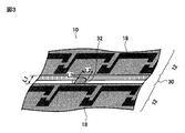
- FIG. 3 is a view showing a method of manufacturing a substrate and a circuit device of the present invention, and is an enlarged perspective view showing a portion where the connecting portion 32 is provided.
- FIG. 1 is a view showing a method of manufacturing a substrate and a circuit device of the present invention, wherein (A) is a plan view and (B) and (C) are cross-sectional views.
- FIG. 2 is a view showing a method of manufacturing a substrate and
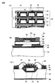
- FIG. 4 is a view showing a method of manufacturing a substrate and a circuit device of the present invention, in which (A) is a plan view showing a partially enlarged substrate, and (B) and (C) are cross-sectional views.
- FIG. 5 is a plan view showing a method of manufacturing a substrate and a circuit device of the present invention.
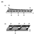
- FIG. 6 is a view showing a circuit device manufactured by the method for manufacturing a circuit device of the present invention, in which (A) is a perspective view and (B) is an enlarged perspective view.
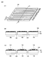
- FIG. 7 is a view showing a substrate of the background art and a method of manufacturing a circuit device using the same, (A) is a perspective view, and (B) and (C) are cross-sectional views.
- the substrate of the present embodiment and a method of manufacturing a circuit device using the substrate will be described with reference to FIGS. 1 to 5.
- dicing processing for providing slits at the boundaries between mounting substrates 12 is performed on the substrate 10.
- a substrate constituting a circuit device in a later step is referred to as the mounting substrate 12, and a large substrate which is a material of the many mounting substrates 12 is referred to as the substrate 10.
- the substrate 10 is a large substrate which is a material of a large number of mounting substrates 12, and as an example of a size in plan view, the length in the longitudinal direction is about 20 cm on the paper The lateral length is about 70 cm.
- the material of the substrate 10 is a metal substrate whose main component is aluminum or copper having a thickness of 1.0 mm or more and 2.0 mm or less (e.g., 1.5 mm).
- a non-organic insulating film mainly made of an oxide film of Al.
- the upper surface of the substrate 10 is entirely covered with an insulating layer made of filler-filled resin, and a conductive pattern is formed on the upper surface of the insulating layer.
- the non-organic insulating film may be omitted.
- the substrate 10 is provided with a plurality of mounting substrates 12 elongated in the lateral direction on the paper surface.
- Each mounting substrate 12 has a rectangular shape provided with two side edges opposed in the longitudinal direction and two side edges opposed in the lateral direction.
- the length in the lateral direction which is the longitudinal direction is about 60 cm
- the length in the longitudinal direction which is the short direction is about 0.6 cm.
- a plurality of LEDs are arranged in a row on the upper surface and used as a lighting device (as an example, a backlight of a liquid crystal display).
- a conductive pattern (not shown) is disposed on the upper surface of each mounting substrate 12. The shape of the conductive pattern will be described later with reference to FIG. 2 (B).
- the mounting substrate region 24 is configured by arranging the five mounting substrates 12 which are elongated in the horizontal direction on the paper surface, but the number of mounting substrates is not limited. Furthermore, the mounting substrates 12 may be arranged in a matrix.
- the mounting board area 24 is configured by arranging a large number of mounting boards 12 next to each other.
- the first support 14, the second support 16, the third support 34, and the fourth support 36 disposed around the periphery of the substrate 10 constitute a frame-like support surrounding the mounting substrate area 24. ing. Further, dicing lines 44 are provided at the boundaries between the mounting substrates 12 and along the dicing lines 44, the substrate 10 is ground into a groove shape to form slits described later.
- connection portion 32 is a region in which the substrate 10 is partially left without being cut in the thickness direction in the middle of the dicing line 44.
- three connecting portions 32 are arranged at equal intervals along the dicing line 44, the number of connecting portions 32 to be provided is arbitrary.
- the cut 26 is temporarily moved in the direction away from the substrate 10. Specifically, referring to FIG. 1 (B), in this step, the cut 26 rotating at high speed is moved rightward on the paper surface along the dicing line 44 shown in FIG. 1 (A). Thus, the substrate 10 is removed in the form of a groove to form a slit 30.
- the lower end of the cut 26 penetrates the substrate 10 and reaches the lower side.
- a dicing sheet may be attached to the lower surface of the substrate 10. Referring to FIG. 1C, when cutting the substrate 10 in the portion provided with the connecting portion 32, the cut 26 is temporarily pulled up and down. That is, in the area in which the connecting portion 32 is provided, the cut-off 26 moves upward while moving rightward on the drawing, and then moves downward thereafter. By doing this, for example, the connecting portion 32 having a thickness of about half or less of that of the substrate 10 is formed. The processing by the above-described cut 26 is performed along each dicing line 44.
- the shape of the slit 30 formed by the said process changes with shapes of the blade tip of the cut-sew 26 used. That is, if the shape of the cutting edge of the cut 26 is a straight shape, the side surface of the slit 30 to be formed is a surface perpendicular to the main surface of the substrate 10. On the other hand, if the cutting edge shape of the cut-out 26 is V-shaped, the side surface of the formed slit 30 is an inclined surface in which the lower side is inclined outward. Furthermore, in the above description, the slits 30 and the connecting portions 32 are formed by grinding of the cut 26. However, these may be formed by other processing methods such as pressing or etching. The configuration of the substrate 10 processed by the above process will be described with reference to FIG.
- groove-shaped slits 30 are provided between the mounting boards 12.
- the mounting substrate area 24 is provided from the plurality of mounting boards 12 provided adjacent to each other, and the slits 30 are formed from the left end to the right end of the mounting board area 24.
- the connecting portion 32 in which the thickness portion of the substrate 10 is left is provided in the middle of each slit 30, and the side edges of the mounting boards 12 adjacent to each other are continuous via the connecting portion 32. ing.
- the details of the connecting portion will be described later with reference to FIG.
- the upper side of the mounting substrate 12 disposed at the upper end of the mounting substrate region 24 is connected to the third support portion 34 via the connecting portion 32 in the drawing.
- conductive pattern 18 formed on the upper surface of mounting substrate 12 has wiring 18B functioning as a path connecting pads with pads 18A to which light emitting elements are connected in a later step.
- connection pad 18C disposed at the end of the mounting substrate 12 and functioning as an external connection electrode.
- the plurality of pads 18A are arranged at equal intervals along the longitudinal direction of the mounting substrate 12. When light emitting elements are connected to these pads, the light emitting elements are connected in series.
- the upper surfaces of the conductive pattern 18 and the insulating layer 38 may be coated with a resist made of resin except for the pad 18A and the connection pad 18C.
- the color of the resist may be white in order to efficiently reflect the light reflected from the light emitting element, or black in order not to reflect the color of the substrate on the light emitted.
- the entire width may be occupied by the conductive pattern by providing a minimum separation width. Also, it may be filled with a dummy conductive pattern.
- the conductive pattern can be plated with Au, Ag, Ni or the like to make the substantially entire reflection region.
- FIG. 2D is a plan view showing the vicinity of the left upper end of the substrate 10 shown in FIG. 2A in an enlarged manner.
- the left end of the slit 30 provided by penetrating the substrate like a groove is L-shaped or T-shaped.
- the left end of the slit 30 disposed at the upper end on the paper surface is L-shaped, and the left end of the other slits 30 is T-shaped.
- Such an end shape of the slit 30 is realized by pressing using a mold or router processing. By making the end portion of the slit 30 into this shape, the width of the continuous portion 22 between the mounting substrate 12 and the first support portion 14 becomes thinner than the mounting substrate 12.
- FIG. 3 is a perspective view showing a connecting portion 32 connecting the mounting boards 12 to each other.
- a slit 30 having a width L1 of about 0.08 mm or more and about 2.0 mm or less is provided between the mounting substrates 12 elongated in the lateral direction on the drawing sheet by dicing in the previous step.
- the connecting portion 32 in which the thick portion of the substrate is partially left is provided instead of the substrate 10 being separated into a groove shape in the entire region.
- the connecting portion 32 is formed by temporarily moving the cut-off upward when forming the slit 30 by grinding the substrate 10 with the cut-off as described with reference to FIG. 1. Ru.
- the connecting portion 32 has a shape in which the upper surface is curved along the longitudinal direction of the slit 30 in the drawing.
- the width L2 of the connecting portion 32 is about 0.5 cm to 1.0 cm, and the height L3 is about 0.5 mm to 1.0 mm.
- the connecting portion 32 is set to a size that can be easily cut by press processing or the like in a later process, while holding the state in which the mounting substrates 12 are connected to each other.
- the point of this embodiment is to connect the side edges in the longitudinal direction of the mounting substrate 12 formed in an elongated shape via the connecting portion 32.
- the mounting substrate 12 provided inside the substrate 10 is formed extremely elongated.
- the length in the lateral direction in the drawing is about 60 cm
- the length in the longitudinal direction is about 0.6 cm. If such an elongated mounting substrate 12 is held by only connecting the left and right ends to the first support portion 14 and the second support portion 16, the mounting substrate 12 may be bent.
- connection part 32 may be provided in the vicinity of the central side of the side of the mounting substrate 12, or a plurality of the connection parts 32 may be provided along the side of the mounting substrate 12, etc. It may be provided at intervals.
- the upper side of the mounting substrate 12 disposed at the upper end of the mounting substrate region 24 is connected to the third support portion 34 of the substrate 10 via the connecting portion 32 in the drawing.
- the lower side of the mounting substrate 12 disposed at the lower end of the mounting substrate region 24 is connected to the fourth support portion 36 of the substrate 10 via the connecting portion 32.
- the plurality of mounting substrates 12 included in the mounting substrate region 24 are supported by the third support portion 34 and the fourth support portion 36 via the connection portions 32, so that the curvature of the mounting substrate 12 is suppressed.
- the effect is greater.
- the slits 30 formed by dicing are formed to be narrower than those of the background art by press processing.
- the width L1 of the slit 30 depends on the width of the cut 26 used (see FIG. 1B), it is about 0.08 mm or more and 2.0 mm or less as described above, and is narrower than the background art.
- the slits 30 By narrowing the slits 30 in this manner, the number of substrate portions discarded due to the provision of the slits 30 decreases, and as a result, a larger number of mounting substrates 12 are manufactured from one substrate 10 than in the background art, The yield is improved.
- FIG. 4A is a plan view showing the substrate 10 which has undergone this step
- FIG. 4B is a cross sectional view showing a mounting structure
- FIG. 4A is a plan view showing the substrate 10 which has undergone this step
- FIG. 4B is a cross sectional view showing a mounting structure
- FIG. 4A is a plan view showing the substrate 10 which has undergone this step
- FIG. 4B is a cross sectional view showing a mounting structure
- FIG. 4C is a cross sectional view showing another mounting structure. is there.
- pads formed of conductive patterns 18 are provided at equal intervals in the longitudinal direction, and the light emitting device 50 is connected to the pads.
- the plurality of light emitting devices 50 are connected in series on the upper surface of each mounting substrate 12.
- the shipping element such as the LED may be connected to the conductive pattern 18 in a resin-sealed package state, or may be connected to the conductive pattern in a non-packaged bare chip state.
- the structure on which the light emitting device 50 in which the LED is resin-sealed is mounted will be described with reference to FIG. 4 (B).
- the light emitting device 50 includes a mounting substrate 52, a light emitting element 62 mounted on the top surface of the mounting substrate 52, a reflection frame 56 fixed on the top surface of the mounting substrate 52 so as to surround the light emitting element 62, and a light emitting element 62.
- the configuration includes a sealing resin 58 for stopping and a conductive path 54 electrically connected to the light emitting element 62.
- the mounting substrate 52 is made of a resin material such as glass epoxy resin or an inorganic material such as ceramic, and has a function of mechanically supporting the light emitting element 62.
- the light emitting element 62 and the reflection frame 56 are disposed on the top surface of the mounting substrate 52.
- the reflection frame 56 is formed of a metal such as aluminum in a frame shape, and the inner side surface is an inclined surface located at the lower side than the upper side. Accordingly, light emitted laterally from the side surface of the light emitting element 62 is reflected upward at the inner side surface of the reflection frame 56.
- the conductive paths 54 are routed from the upper surface to the lower surface of the mounting substrate 52.
- the conductive path 54 is electrically connected to the light emitting element 62 through the metal thin wire 60 on the upper surface of the mounting substrate 52.
- the conductive path 54 formed on the lower surface of the mounting substrate 52 is connected to the conductive pattern 18 formed on the substrate 10 via a bonding material 64 such as solder.
- the light emitting element 62 is mounted in a bare chip state without being packaged
- the light emitting element 62 is disposed in the recess 70 in which the upper surface of the substrate 10 is recessed, but other configurations are also possible.
- the light emitting element 62 may be fixed to the upper surface of the substrate 10 which is a flat surface, or the light emitting element 62 may be fixed to the upper surface of the island-shaped conductive pattern 18.
- the upper and lower surfaces of the substrate 10 are covered with oxide films 66 and 68, respectively.
- the oxide film 66 and the insulating layer 38 are removed in the recess 70 and the periphery thereof.
- Two electrodes are provided on the top surface of the light emitting element 62, and these electrodes are connected to the conductive pattern 18 via the metal thin wires 60.
- the light emitting element 62 is fixed to the bottom surface 74 of the recess 70 via the bonding material 76.
- two electrodes are disposed on the top surface of the light emitting element 62, but an anode electrode (or a cathode electrode) may be provided on the top surface, and an anode electrode (or a cathode electrode) may be disposed on the bottom surface.
- each mounting substrate 12 is separated from the substrate 10.
- the separation in this step can be performed by a pressing method using a mold, a cutting method rotating at high speed, or a separation method such as laser irradiation.
- the end portion of each mounting substrate 12 is separated from the first support portion 14 by cutting the continuous portion 22 along a cutting line 28 indicated by an alternate long and short dash line.
- the mounting substrate 12 is separated by easily cutting the continuous portion 22. Further, the connecting portion 32 for connecting the mounting substrates 12 to one another is also cut along the cutting line 42. As described above, since the thickness of the connecting portion 32 is thinner than the mounting substrate 12, the connecting portion 32 is easily cut.
- a circuit device having a configuration in which the light emitting device 50 is mounted on the mounting substrate 12 is manufactured. In the above process, only the light emitting element is mounted on the top surface of the mounting substrate 12, but a hybrid integrated circuit device may be configured in which other circuit elements such as transistors and ICs are incorporated on the top surface of the mounting substrate 12. good.
- the upper surface, the side surface, and the lower surface of the mounting substrate including the light emitting device 50 may be covered with a sealing resin by transfer molding or potting.
- separation processing for separating the mounting boards 12 is performed after element mounting, but this order may be reversed. That is, it is transported in the state of the substrate 10 provided with a large number of mounting substrates 12 to a factory where element mounting is performed, and the substrate 10 is separated into individual mounting substrates 12 and mounting of each element on the mounting substrate 12 is performed. It is good.
- the structure of the circuit device 90 manufactured by the above manufacturing method will be described with reference to FIG.
- the circuit device 90 includes a mounting substrate 12 elongated in the lateral direction in the drawing, an insulating layer 38 covering the upper surface of the mounting substrate, a conductive pattern 18 of a predetermined shape provided on the upper surface of the insulating layer 38, and the conductive pattern 18. It mainly comprises a large number of light emitting devices 50 connected. The details of each of these elements are as described above.
- the mounting substrate 12 is a very elongated substrate having a lateral length of, for example, 60 cm in the drawing and a width of 0.6 cm in the depth direction. If the shape of the cutting edge of the cut-off shown in FIG. 1B is a straight shape, the side surface of the mounting substrate 12 is a top surface and is a vertical surface.
- the side surface of the mounting substrate 12 is an inclined surface whose lower portion is inclined outward.
- the connection part 32 which is a projection part which protrudes outside about 1 mm is provided in the side surface of a longitudinal direction.
- the connecting portion 32 can be used by biting into the inner wall of the set when the circuit device 90 is assembled in a set such as a lighting fixture.
- each connecting portion 32 may be flattened by performing pressing processing from the side, or the connecting portion 32 is removed from the side surface of the mounting substrate 12 by grinding or the like. You may.
- the pressing process it is possible to press the burr generated at the time of processing the mounting substrate 12 against the side surface of the mounting substrate 12 to be integrated. Furthermore, at this time, when the connecting portion 32 is removed from the mounting substrate 12, the mounting substrate 12 near the connecting portion 32 may be removed simultaneously. By doing this, the mounting substrate 12 at the location where the connecting portion 32 exists becomes concave in plan view.
Landscapes
- Engineering & Computer Science (AREA)
- Manufacturing & Machinery (AREA)
- Microelectronics & Electronic Packaging (AREA)
- Structure Of Printed Boards (AREA)
Abstract
搬送工程の途中段階に於ける基板の湾曲が抑制された基板およびそれを用いた回路装置の製造方法を提供する。本発明の基板10は、横方向に細長い複数の実装基板12と、実装基板12同士の間に配置されたスリット30と、隣接する実装基板12の側辺同士を連結すると共に前記実装基板12よりも厚みが薄い連結部32とを備えている。実装基板12の長手方向の側辺同士が連結部32を介して連結されることにより、基板10を搬送する段階に於ける実装基板12の撓みが抑制される。
Description
本発明は、基板およびそれを用いた回路装置の製造方法に関する。特に本発明は、一方方向に細長い実装基板が複数個連結された基板およびそれを用いた回路装置の製造方法に関する。
回路基板上に実装された回路素子から成る回路装置を形成する場合、一枚の大型の基板の上面に多数個のユニットを構成する導電パターンを構成して、導電パターンに回路素子を接続した後に、各ユニットを分離する方法が従来から採用されている(下記特許文献1参照)。
図7(A)の斜視図を参照して、この様な回路装置の製造方法に用いられる大判基板100の構成を説明する。
基板100は、アルミニウム等の金属から成る厚みが1.5mm程度の基板であり、具体的な大きさの一例としては、紙面上の奥行き方向の幅が20cm程度であり、横方向の長さが70cm程度である。
この様な大きさの基板100の内部に多数個の実装基板106が設けられている。1つの実装基板106の大きさは、横方向の長さが60cm程度であり、幅L10が0.6cm程度である。即ち、実装基板106は横方向に極めて細長く形成される基板である。この様な形状の実装基板106は、LCD等のモニタに内蔵されるバックライトの基板として仕様される。
また、各実装基板106同士の間には、基板100を部分的に打ち抜いて除去したスリット120が設けられている。このスリット120の横方向の長さは実装基板106と同様であり、幅L11は2mm程度である。即ち、各実装基板106は、左右端部が基板100の枠状の支持部と連結されることで、全体として一体の基板状態を保持している。
図7(B)および図7(C)を参照して、上記した構成の基板100を使用した回路装置の製造方法を説明する。
図7(B)を参照して、金属から成る各実装基板106の上面は、樹脂から成る絶縁層102により被覆されている。更に、絶縁層102の上面には所定形状の導電パターン104が形成されている。
図7(C)を参照して、各実装基板106の導電パターン104に、回路素子112を実装する。回路素子112としては、発光素子であるLEDやトランジスタ等の他の素子が採用される。
回路素子112の実装が終了した後は、図7(A)を参照して、各実装基板106の左右両端部を、基板100の枠状の支持部から切断する。各実装基板106の切断は、プレス加工またはダイシング加工により行われる。
しかしながら、上記した回路装置の製造方法では、製造工程の途中段階にて各実装基板106が湾曲してしまう問題があった。
具体的には、図7(A)を参照すると、大判の基板100に設けられる実装基板106は、横方向に極めて細長い形状である。そして、この実装基板106は両端が基板100の枠状の支持部により支持されているのみであり、長手方向の中間部は機械的に支持されていない。従って、製造工程の途中段階にて基板100の端部を保持して搬送しようとすると、各実装基板106が自重で撓んでしまい、この撓みにより上面に形成された導電パターンや回路素子が破壊されてしまう恐れがある。更には、実装基板106の撓みが大きいと、実装基板106自体が変形してしまう場合もある。
更に、打ち抜き加工により基板100を除去して設けられるスリット120の幅L11は0.2cm程度であり、実装基板120の幅L10が0.6cmであることを考慮すると、基板100の約1/3がスリット120の為に除去して廃棄されることとなる。更にまた、打ち抜き加工によりよって、幅L11が0.2cmよりも狭いスリット120を形成することは困難であった。このことから、基板100の収率を向上させることが容易ではなかった。
本発明は上記した問題を鑑みてなされ、本発明の目的は、搬送工程の途中段階に於ける基板の湾曲が抑制された基板およびそれを用いた回路装置の製造方法を提供することにある。
本発明の基板は、長手方向で対向する2つの側辺と短手方向で対向する2つの側辺を有し、長手方向で対向する前記側辺が隣り合うように配置された複数の実装基板と、前記実装基板の前記長手方向の側辺同士の間に配置されたスリットと、隣接する一方の前記実装基板の前記側辺と、隣接する他方の前記実装基板の前記側辺とを一体的に連結すると共に、前記実装基板よりも厚みが薄い連結部と、を備えたことを特徴とする。
本発明の回路装置の製造方法は、長手方向で対向する2つの側辺と短手方向で対向する2つの側辺を有し、長手方向で対向する前記側辺が隣り合うように配置された複数の実装基板と、前記実装基板の前記長手方向の側辺同士の間に配置されたスリットと、隣接する一方の前記実装基板の前記側辺と、隣接する他方の前記実装基板の前記側辺とを一体的に連結すると共に、前記実装基板よりも厚みが薄い連結部と、備えた基板を用意する工程と、前記各実装基板の主面に設けられた導電パターンに回路素子を電気的に接続する工程と、前記連結部を切断することにより、前記実装基板を個別に分離する工程と、を備えたことを特徴とする。
本発明の回路装置の製造方法は、長手方向で対向する2つの側辺と短手方向で対向する2つの側辺を有し、長手方向で対向する前記側辺が隣り合うように配置された複数の実装基板と、前記実装基板の前記長手方向の側辺同士の間に配置されたスリットと、隣接する一方の前記実装基板の前記側辺と、隣接する他方の前記実装基板の前記側辺とを一体的に連結すると共に、前記実装基板よりも厚みが薄い連結部と、備えた基板を用意する工程と、前記各実装基板の主面に設けられた導電パターンに回路素子を電気的に接続する工程と、前記連結部を切断することにより、前記実装基板を個別に分離する工程と、を備えたことを特徴とする。
本発明の基板は、細長の基板同士の間にスリットが設けられており、隣接する一方の基板の側辺中間部と、隣接する他方の側辺中間部とを、連結部により一体的に連続させている。この様にすることで、長細の基板の中間部が機械的に補強されるので、製造工程にて大判の基板を搬送する際に、実装基板106が自重により撓むことが抑制される。
更に本発明では、この連結部の幅を実装基板よりも薄くしている。このことにより、実装基板106に発光素子等の回路素子を実装した後の工程にて、連結部を容易に切断することが可能となる。
更に本発明では、この連結部の幅を実装基板よりも薄くしている。このことにより、実装基板106に発光素子等の回路素子を実装した後の工程にて、連結部を容易に切断することが可能となる。
図1は本発明の基板および回路装置の製造方法を示す図であり、(A)は平面図であり、(B)および(C)は断面図である。
図2は本発明の基板および回路装置の製造方法を示す図であり、(A)は平面図であり、(B)は断面図であり、(C)は一つの実装基板12を示す平面図であり、(D)は基板10の一部分を拡大して示す平面図である。
図3は本発明の基板および回路装置の製造方法を示す図であり、連結部32が設けられる箇所を拡大して示す斜視図である。
図4は本発明の基板および回路装置の製造方法を示す図であり、(A)は基板を部分的に拡大して示す平面図であり、(B)および(C)は断面図である。
図5は本発明の基板および回路装置の製造方法を示す平面図である。
図6は本発明の回路装置の製造方法により製造される回路装置を示す図であり、(A)は斜視図であり、(B)は拡大して示す斜視図である。
図7は背景技術の基板およびそれを用いた回路装置の製造方法を示す図であり、(A)は斜視図であり、(B)および(C)は断面図である。
図1から図5を参照して、本形態の基板およびそれを用いた回路装置の製造方法を説明する。
図1を参照して先ず、基板10に対して、実装基板12同士の境界にスリットを設けるためのダイシング加工を行う。ここでは、後の工程にて回路装置を構成する基板を実装基板12と称し、多数の実装基板12の材料となる大判基板を基板10と称する。
図1(A)を参照して、基板10は、多数の実装基板12の材料となる大判基板であり、平面視の大きさの一例としては、紙面上にて縦方向の長さが20cm程度であり、横方向の長さが70cm程度である。基板10の材料は、厚みが1.0mm以上2.0mm以下(例えば1.5mm)のアルミニウムや銅を主成分とする金属基板である。基板10の材料としてアルミニウムが採用される場合は、両主面はAlの酸化膜を主とした非有機性絶縁膜により被覆される。更に、基板10の上面は、フィラーが充填された樹脂から成る絶縁層により全面的に被覆されており、この絶縁層の上面に導電パターンが形成されている。尚、非有機性絶縁膜は、省略されても良い。
基板10には、紙面上にて横方向に細長く伸びる複数の実装基板12が設けられている。各実装基板12は、長手方向で対向する2つの側辺と、短手方向で対向する2つの側辺を備える矩形形状である。実装基板12のサイズの一例としては、長手方向である横方向の長さが60cm程度であり、短手方向である縦方向の長さが0.6cm程度である。本形態の実装基板12は、例えば、上面に複数個のLEDが列状に配置されて照明装置(一例として液晶ディスプレイのバックライト)として用いられる。各実装基板12の上面には不図示の導電パターンが配置されるが、この導電パターンの形状は図2(B)を参照して後述する。
ここでは、紙面上にて横方向に細長い5つの実装基板12が配置されることで、実装基板領域24が構成されているが、実装基板の個数は限定されない。更には、実装基板12がマトリックス状に配置されても良い。
ここでは、多数個の実装基板12が隣設されることにより実装基板領域24が構成されている。そして、基板10の周辺部に配置された第1支持部14、第2支持部16、第3支持部34および第4支持部36により、実装基板領域24を囲む枠状の支持部が構成されている。
また、各実装基板12同士の境界には、ダイシングライン44が設けられており、このダイシングライン44に沿って、基板10を溝状に研削加工することにより後述するスリットが形成される。
連結部32は、ダイシングライン44の途中部分に於いて、基板10を厚み方向に切断せずに部分的に残存させる領域である。ここでは、連結部32は、ダイシングライン44に沿って等間隔に3つが配置されているが、設けられる連結部32の個数は任意である。
本工程では、実装基板12同士の間にスリットを設けるために、カットソーによる研削加工を行う。しかしながら、連結部32では、一時的にカットソー26を基板10から離間する方向に移動させている。
具体的には、図1(B)を参照して、本工程では、図1(A)に示すダイシングライン44に沿って、高速で回転するカットソー26を紙面上にて右方向に移動させることにより、基板10を溝状に除去してスリット30が形成される。従って、カットソー26の下端は、基板10を貫通して下方まで到っている。また、本工程によるカットソーの破損を防止するために、基板10の下面にダイシングシートを貼着しても良い。
図1(C)を参照して、上記した連結部32が設けられた部分の基板10を切断する際には、カットソー26は上下方向に一時的に引き上げられる。即ち、連結部32が設けられる領域では、カットソー26は、紙面上にて右方向に向かって移動しながら上方に移動し、更にその後に下方に移動する。この様にすることで、例えば、基板10の半分以下程度の厚さを有する連結部32が形成される。
上記したカットソー26による加工は、各ダイシングライン44に沿って行われる。
また、上記工程により形成されるスリット30の形状は、使用されるカットソー26の刃先の形状により異なる。即ち、カットソー26の刃先の形状がストレート形状であれば、形成されるスリット30の側面は基板10の主面に対して垂直な面となる。一方、カットソー26の刃先形状がV字型形状であれば、形成されるスリット30の側面は、下方の方が外側に傾斜する傾斜面となる。
更にまた、上記説明ではカットソー26の研削加工によりスリット30および連結部32を形成したが、プレス加工やエッチング加工等の他の加工方法によってもこれらを形成することが可能である。
図2を参照して、上記工程により加工された基板10の構成を説明する。
図2(A)および図2(B)を参照して、各実装基板12同士の間には、溝状のスリット30が設けられている。本形態では、隣設する複数の実装基板12から実装基板領域24が設けられており、各スリット30は実装基板領域24の左端から右端に到るまで形成されている。
上記したように、各スリット30の途中には、基板10の厚み部分を残存させた連結部32が設けられており、この連結部32を介して隣接する実装基板12同士の側辺が連続している。この連結部の詳細は図3を参照して後述する。
更に、紙面上にて、実装基板領域24の上端に配置された実装基板12の上側側辺は、連結部32を経由して第3支持部34と連結されている。また、実装基板領域24の下端に配置された実装基板12の下側側辺も同様に、複数の連結部32を介して第4支持部36と連結されている。
図2(C)を参照して、実装基板12の上面に形成される導電パターン18は、後の工程で発光素子が接続されるパッド18Aと、パッド同士を接続する経路として機能する配線部18Bと、実装基板12の端部に配置されて外部接続電極として機能する接続パッド18Cとを備えている。ここでは、実装基板12の長手方向に沿って等間隔に複数個のパッド18Aが配置されており、これらのパッドに発光素子を接続すると、発光素子は直列に接続される。
また、図示はされていないが、導電パターン18および絶縁層38の上面は、パッド18Aおよび接続パッド18Cを除外して、樹脂から成るレジストにより被覆されても良い。このレジストの色としては、発光素子から反射された光を効率的に反射させるために白色にしても良いし、基板の色を発光される光に反映させないために黒色にしても良い。一方、白色レジストの劣化を考えると、最小限の分離幅を設け、全域を導電パターンで占有してもよい。またダミー導電パターンで埋めても良い。この場合、導電パターンにAu、AgまたはNi等のメッキが施せ、実質全体を反射領域と出来る。
図2(D)は、図2(A)に示す基板10の左側上端部付近を拡大して示す平面図である。この図を参照すると、基板を溝状に貫通して設けたスリット30の左側の端部は、L字形状またはT字形状を呈している。紙面上にて上端に配置されたスリット30の左端はL字形状であり、その他のスリット30の左端はT字形状である。この様なスリット30の端部形状は、金型を用いたプレス加工またはルーター加工により実現される。
スリット30の端部をこの形状にすることで、実装基板12と第1支持部14との連続部22の幅が、実装基板12よりも細くなる。例えば、連続部22の幅L5が6.0mmであれば、連続部の幅L6は3.0mm以下と半分以下程度にされる。この様に、幅が狭い連続部22を介して、実装基板12の端部と第1支持部14が連続することにより、後の工程にて、細長い連続部22を切断するのみで容易に実装基板12を第1支持部14から分離出来る。
図3は、実装基板12同士を連結する連結部32を示す斜視図である。紙面上にて横方向に細長い実装基板12同士の間には、先工程のダイシングにより、幅L1が0.08mm以上2.0mm以下程度のスリット30が設けられている。
スリット30が設けられた領域では、全域に渡り溝状に基板10が分離されるのではなく、部分的に基板の厚み部分を残存させた連結部32が設けられている。この連結部32は、図1を参照して説明したように、カットソーにて基板10を研削加工することでスリット30を形成する際に、一時的にカットソーを上方向に移動させることで形成される。
連結部32は、紙面上ではスリット30の長手方向に沿って上面が湾曲する形状を呈している。連結部32の幅L2は0.5cmから1.0cm程度であり、高さL3は0.5mmから1.0mm程度である。連結部32は、各実装基板12同士が連結された状態を保持すると共に、後の工程にてプレス加工等により容易に切断できる大きさに設定される。
本形態のポイントは、細長く形成される実装基板12の長手方向の側辺同士を、連結部32を介して連結することにある。
具体的には、図2(A)を参照して、基板10の内部に設けられる実装基板12は極めて細長く形成される。具体的には、紙面上に於ける横方向の長さは60cm程度であり、縦方向の長さは0.6cm程度である。この様な細長の実装基板12を、左右両端が第1支持部14および第2支持部16に連結されるのみで保持すると、実装基板12が撓む恐れがある。具体的には、基板10の支持部を保持することにより搬送しようとすると、実装基板12の自重により中間部付近が下方に撓み、上面に形成された導電パターンや回路素子が破壊されてしまう恐れがある。
そこで本形態では、実装基板12の長手方向の側辺同士を、連結部32を介して連結している。この様にすることで、連結部32を介して隣接された実装基板12同士が補強されるので、実装基板12が搬送する際に撓むことが抑制される。設けられる連結部32の数としては、1つの連結部32が実装基板12の側辺中央部付近に設けられても良いし、複数個の連結部32が実装基板12の側辺に沿って等間隔に設けられても良い。
更に、紙面上にて、実装基板領域24の上端に配置された実装基板12の上側側辺は、連結部32を介して、基板10の第3支持部34に連結されている。同様に、実装基板領域24の下端に配置された実装基板12の下側側辺は、連結部32を介して、基板10の第4支持部36に連結されている。このことにより、実装基板領域24に含まれる複数の実装基板12が、連結部32を経由して第3支持部34および第4支持部36に支持されるので、実装基板12の湾曲を抑制する効果が大きくなる。
更に、図3を参照して、ダイシングにより形成されるスリット30は、プレス加工による背景技術のものよりも幅が狭く形成される。スリット30の幅L1は、使用されるカットソー26(図1(B)参照)の幅によるが、上記したように0.08mm以上2.0mm以下程度であり、背景技術よりも狭い。この様にスリット30を狭くすることにより、スリット30が設けられることにより破棄される基板部分が少なくなり、結果的に1枚の基板10から背景技術よりも多数個の実装基板12が製造され、収率が改善される。
図4を参照して、次に、各実装基板12に回路素子として発光装置を実装する。図4(A)は本工程を経た基板10を示す平面図であり、図4(B)は実装の構造を示す断面図であり、図4(C)は他の実装構造を示す断面図である。
図4(A)を参照して、各実装基板12には、長手方向に等間隔で導電パターン18から成るパッドが設けられており、このパッドに発光装置50が接続される。本工程の接続を行うことにより、各実装基板12の上面にて、複数個の発光装置50が直列に接続される。
ここで、LED等の発送素子は、樹脂封止されたパッケージの状態で導電パターン18に接続されても良いし、パッケージされていないベアチップの状態で導電パターンに接続されても良い。
図4(B)を参照して、LEDが樹脂封止された発光装置50が実装される構造を説明する。
発光装置50は、実装基板52と、実装基板52の上面に実装された発光素子62と、発光素子62を取り囲むように実装基板52の上面に固着された反射枠56と、発光素子62を封止する封止樹脂58と、発光素子62と電気的に接続される導電路54とを備えた構成と成っている。
実装基板52は、ガラスエポキシ樹脂等の樹脂材料やセラミック等の無機物から成り、発光素子62を機械的に支持する機能を有する。実装基板52の上面に発光素子62および反射枠56が配置される。
反射枠56は、アルミニウム等の金属を額縁状に形成したものであり、内側の側面は上部よりも下部が内側に位置する傾斜面と成っている。従って、発光素子62の側面から側方に発光された光は、反射枠56の内側の側面で上方に反射される。
導電路54は、実装基板52の上面から下面まで引き回されている。実装基板52の上面において導電路54は金属細線60を経由して発光素子62と電気的に接続される。そして、実装基板52の下面に形成された導電路54は、半田等の接合材64を介して、基板10に形成された導電パターン18と接続されている。
図4(C)を参照して、発光素子62がパッケージ化されずにベアチップの状態で実装される構造を説明する。この図では、基板10の上面を窪ませた凹部70に発光素子62が配置されているが、他の構成も採用可能である。例えば、平坦面である基板10の上面に発光素子62が固着されても良いし、アイランド形状の導電パターン18の上面に発光素子62が固着されても良い。また、基板10の上面および下面は酸化膜66、68により被覆される。そして、凹部70およびその周辺部では、酸化膜66および絶縁層38は除去されている。
発光素子62の上面には、2つの電極(アノード電極、カソード電極)が設けられ、これらの電極は金属細線60を経由して、導電パターン18と接続される。また、この凹部70の底面74に発光素子62が、接合材76を介して固着されている。
ここでは、発光素子62の上面に2つの電極が配置されているが、上面にアノード電極(又はカソード電極)が設けられ、下面にアノード電極(又はカソード電極)が配置されても良い。この場合は、発光素子62の上面の電極が金属細線60を介して導電パターン18と接続され、下面の電極がランド状の導電パターンに半田等の導電性接合材を介して接続される。
図5を参照して、次に、基板10から各実装基板12を分離する。本工程の分離は、金型を用いたプレス加工、高速で回転するカットソーまたはレーザー照射等の分離方法で行える。
本工程では、一点鎖線で示す切断線28にて連続部22を切断することにより、各実装基板12の端部を第1支持部14から分離している。上記したように、連続部22の幅は実装基板12の半分以下程度に狭いので、連続部22を容易に切断することで各実装基板12の分離が行われる。
また、実装基板12同士を連続させる連結部32も、切断線42にて切断される。上記したように、連結部32の厚みは、実装基板12よりも薄く形成されるので、連結部32は容易に切断される。
以上の工程により、実装基板12に発光装置50が実装された構成の回路装置が製造される。また、上記工程では、発光素子のみが実装基板12の上面に実装されていたが、トランジスタやIC等の他の回路素子が実装基板12の上面に組み込まれた混成集積回路装置が構成されても良い。更には、トランスファーモールドやポッティングにより、発光装置50を含む実装基板の上面、側面および下面が、封止樹脂により被覆されても良い。
ここで、上記説明では、素子実装を行った後に、各実装基板12を分離する分離加工を行ったが、この順番を逆にしても良い。即ち、素子実装を行う工場まで、多数の実装基板12が設けられた基板10の状態で搬送し、基板10を個々の実装基板12に分離した後に、各素子の実装基板12への実装を行っても良い。
図6を参照して、上記製造方法により製造される回路装置90の構造を説明する。回路装置90は紙面上にて横方向に細長い実装基板12と、実装基板の上面を被覆する絶縁層38と、絶縁層38の上面に設けられた所定形状の導電パターン18と、導電パターン18に接続された多数の発光装置50とを主要に備えている。これらの各要素の詳細は、上記した通りである。
実装基板12は、紙面上にて横方向の長さが例えば60cmであり、奥行き方向の幅が0.6cmである非常に細長い基板である。また、図1(B)に示すカットソーの刃先の形状がストレート形状であれば、実装基板12の側面は上面にして垂直な面となる。一方、使用されるカットソー26の刃先がV字型の断面を備えている場合は、実装基板12の側面は、下部が外側に向かって傾斜する傾斜面となる。
そして、長手方向の側面に、1mm程度外側に突起する突起部である連結部32が設けられている。この連結部32は、回路装置90を照明器具等のセットに組み組む際に、セットの内壁に食い込ませて用いることが可能である。
また、突起する連結部32が不要であれば、側方から押圧加工を施すことにより各連結部32を平坦化させても良いし、グラインディング等により連結部32を実装基板12の側面から除去しても良い。押圧加工を行うことにより、実装基板12を加工する際に発生したバリを、実装基板12の側面に押しつけて一体化させることが出来る。
更にここで、連結部32を実装基板12から除去する際に、連結部32付近の実装基板12を同時に除去しても良い。この様にすることで、連結部32が存在する箇所の実装基板12が平面視で凹状となる。
10 基板
12 実装基板
14 第1支持部
16 第2支持部
18 導電パターン
18A パッド
18B 配線部
18C 接続パッド
22 連続部
24 実装基板領域
26 カットソー
28 切断線
30 スリット
32 連結部
34 第3支持部
36 第4支持部
38 絶縁層
42 切断線
44 ダイシングライン
50 発光装置
52 実装基板
54 導電路
56 反射枠
58 封止樹脂
60 金属細線
62 発光素子
64 接合材
66 酸化膜
68 酸化膜
70 凹部
74 底面
76 接合材
12 実装基板
14 第1支持部
16 第2支持部
18 導電パターン
18A パッド
18B 配線部
18C 接続パッド
22 連続部
24 実装基板領域
26 カットソー
28 切断線
30 スリット
32 連結部
34 第3支持部
36 第4支持部
38 絶縁層
42 切断線
44 ダイシングライン
50 発光装置
52 実装基板
54 導電路
56 反射枠
58 封止樹脂
60 金属細線
62 発光素子
64 接合材
66 酸化膜
68 酸化膜
70 凹部
74 底面
76 接合材
Claims (9)
- 長手方向で対向する2つの側辺と短手方向で対向する2つの側辺を有し、長手方向で対向する前記側辺が隣り合うように配置された複数の実装基板と、
前記実装基板の前記長手方向の側辺同士の間に配置されたスリットと、
隣接する一方の前記実装基板の前記側辺と、隣接する他方の前記実装基板の前記側辺とを一体的に連結すると共に、前記実装基板よりも厚みが薄い連結部と、
を備えたことを特徴とする基板。 - 複数の前記実装基板の短手方向で対向する側辺と連続する支持部を更に備えることを特徴とする請求項1記載の基板。
- 1つの前記スリットに対して、複数個の前記連結部を離間して設けることを特徴とする請求項2記載の基板。
- 前記複数の前記実装基板により実装基板領域が構成され、
前記実装基板領域の端部に配置された前記実装基板の長手方向の側辺は、前記連結部を介して前記基板の支持部を連結されることを特徴とする請求項3記載の基板。 - 前記実装基板の短手方向の側辺は、前記実装基板よりも細く形成される連続部を経由して前記支持部と連続することを特徴とする請求項4記載の基板。
- 長手方向で対向する2つの側辺と短手方向で対向する2つの側辺を有し、長手方向で対向する前記側辺が隣り合うように配置された複数の実装基板と、前記実装基板の前記長手方向の側辺同士の間に配置されたスリットと、隣接する一方の前記実装基板の前記側辺と、隣接する他方の前記実装基板の前記側辺とを一体的に連結すると共に、前記実装基板よりも厚みが薄い連結部と、備えた基板を用意する工程と、
前記各実装基板の主面に設けられた導電パターンに回路素子を電気的に接続する工程と、
前記連結部を切断することにより、前記実装基板を個別に分離する工程と、
を備えたことを特徴とする回路装置の製造方法。 - 前記基板を用意する工程では、カットソーによる研削加工で一括して前記スリットおよび前記連結部を設けることを特徴とする請求項6記載の回路装置の製造方法。
- 前記基板を貫通する深さでカットソーによる研削加工を行うことで前記スリットを設け、前記カットソーの研削加工の深さを前記基板の厚さよりも浅くすることで、前記基板の残りの厚み部分から成る前記連結部を残存させることを特徴とする請求項7記載の回路装置の製造方法。
- 複数個の前記実装基板の短手方向の側辺は、前記実装基板よりも幅が狭い連続部を経由して支持部に連結され、
前記分離する工程では、前記連続部を切断することにより前記各実装基板を前記支持部から分離することを特徴とする請求項8記載の回路装置の製造方法。
Applications Claiming Priority (2)
| Application Number | Priority Date | Filing Date | Title |
|---|---|---|---|
| JP2009-287626 | 2009-12-18 | ||
| JP2009287626 | 2009-12-18 |
Publications (1)
| Publication Number | Publication Date |
|---|---|
| WO2011074684A1 true WO2011074684A1 (ja) | 2011-06-23 |
Family
ID=44167434
Family Applications (1)
| Application Number | Title | Priority Date | Filing Date |
|---|---|---|---|
| PCT/JP2010/072826 Ceased WO2011074684A1 (ja) | 2009-12-18 | 2010-12-13 | 基板およびそれを用いた回路装置の製造方法 |
Country Status (1)
| Country | Link |
|---|---|
| WO (1) | WO2011074684A1 (ja) |
Cited By (1)
| Publication number | Priority date | Publication date | Assignee | Title |
|---|---|---|---|---|
| JP2014010184A (ja) * | 2012-06-27 | 2014-01-20 | Uproad Plans Co Ltd | 2次元配列led照明 |
Citations (3)
| Publication number | Priority date | Publication date | Assignee | Title |
|---|---|---|---|---|
| JPH0540910A (ja) * | 1991-08-02 | 1993-02-19 | Sony Corp | 狭トラツク磁気ヘツドの製造方法 |
| JP2004031777A (ja) * | 2002-06-27 | 2004-01-29 | Nidec Copal Corp | 集合基板 |
| JP2004311849A (ja) * | 2003-04-09 | 2004-11-04 | Ngk Spark Plug Co Ltd | 配線基板およびその製造方法 |
-
2010
- 2010-12-13 WO PCT/JP2010/072826 patent/WO2011074684A1/ja not_active Ceased
Patent Citations (3)
| Publication number | Priority date | Publication date | Assignee | Title |
|---|---|---|---|---|
| JPH0540910A (ja) * | 1991-08-02 | 1993-02-19 | Sony Corp | 狭トラツク磁気ヘツドの製造方法 |
| JP2004031777A (ja) * | 2002-06-27 | 2004-01-29 | Nidec Copal Corp | 集合基板 |
| JP2004311849A (ja) * | 2003-04-09 | 2004-11-04 | Ngk Spark Plug Co Ltd | 配線基板およびその製造方法 |
Cited By (1)
| Publication number | Priority date | Publication date | Assignee | Title |
|---|---|---|---|---|
| JP2014010184A (ja) * | 2012-06-27 | 2014-01-20 | Uproad Plans Co Ltd | 2次元配列led照明 |
Similar Documents
| Publication | Publication Date | Title |
|---|---|---|
| US10249600B2 (en) | Light emitting apparatus, illumination apparatus and display apparatus | |
| TWI657597B (zh) | 側照式發光二極體結構及其製造方法 | |
| CN105990507B (zh) | 侧照式发光二极管结构及其制造方法 | |
| JP2011119557A (ja) | 発光装置及びその製造方法 | |
| JP2011176271A (ja) | Ledパッケージ及びその製造方法 | |
| JP5232394B2 (ja) | 半導体装置の製造方法 | |
| US20140061682A1 (en) | Semiconductor device and method for manufacturing same | |
| JP4615282B2 (ja) | 半導体パッケージの製造方法 | |
| CN106057750A (zh) | 具有低翘曲度的封装结构 | |
| WO2013186982A1 (ja) | フィルム配線基板および発光装置 | |
| JP6677616B2 (ja) | 半導体装置の製造方法 | |
| CN205723519U (zh) | 半导体器件 | |
| JPH11214607A (ja) | 半導体装置 | |
| JP2002064224A (ja) | 発光ダイオード及びその製造方法 | |
| TWI824863B (zh) | 元件基板及其製造方法 | |
| US7531895B2 (en) | Integrated circuit package and method of manufacture thereof | |
| KR20240071319A (ko) | 기판 및 반도체 모듈 | |
| WO2011049234A1 (ja) | 基板およびそれを用いた回路装置の製造方法 | |
| KR20160088746A (ko) | 반도체 패키지 및 반도체 패키지의 제조방법 | |
| KR20130023432A (ko) | 반도체 패키지용 리드 프레임 구조, 이의 제조방법 및 이를 이용한 반도체 패키지 제조방법 | |
| CN103208484B (zh) | 半导体封装及其制造方法 | |
| KR100888180B1 (ko) | 측면 발광 led 조립체 | |
| JP2012227254A (ja) | Led素子用リードフレーム基板及びその製造方法 | |
| JP2018093090A (ja) | 多列型led用リードフレーム | |
| TWI571995B (zh) | 具有多連接導線之設備、具有多連接導線之晶片封裝以及用於保留導線框次結構之外部針腳的方法 |
Legal Events
| Date | Code | Title | Description |
|---|---|---|---|
| 121 | Ep: the epo has been informed by wipo that ep was designated in this application |
Ref document number: 10837708 Country of ref document: EP Kind code of ref document: A1 |
|
| NENP | Non-entry into the national phase |
Ref country code: DE |
|
| 122 | Ep: pct application non-entry in european phase |
Ref document number: 10837708 Country of ref document: EP Kind code of ref document: A1 |
|
| NENP | Non-entry into the national phase |
Ref country code: JP |