WO2011065252A1 - 粘着シート及び電子部品 - Google Patents
粘着シート及び電子部品 Download PDFInfo
- Publication number
- WO2011065252A1 WO2011065252A1 PCT/JP2010/070348 JP2010070348W WO2011065252A1 WO 2011065252 A1 WO2011065252 A1 WO 2011065252A1 JP 2010070348 W JP2010070348 W JP 2010070348W WO 2011065252 A1 WO2011065252 A1 WO 2011065252A1
- Authority
- WO
- WIPO (PCT)
- Prior art keywords
- meth
- adhesive sheet
- mass
- pressure
- sensitive adhesive
- Prior art date
- Legal status (The legal status is an assumption and is not a legal conclusion. Google has not performed a legal analysis and makes no representation as to the accuracy of the status listed.)
- Ceased
Links
Images
Classifications
-
- C—CHEMISTRY; METALLURGY
- C09—DYES; PAINTS; POLISHES; NATURAL RESINS; ADHESIVES; COMPOSITIONS NOT OTHERWISE PROVIDED FOR; APPLICATIONS OF MATERIALS NOT OTHERWISE PROVIDED FOR
- C09J—ADHESIVES; NON-MECHANICAL ASPECTS OF ADHESIVE PROCESSES IN GENERAL; ADHESIVE PROCESSES NOT PROVIDED FOR ELSEWHERE; USE OF MATERIALS AS ADHESIVES
- C09J133/00—Adhesives based on homopolymers or copolymers of compounds having one or more unsaturated aliphatic radicals, each having only one carbon-to-carbon double bond, and at least one being terminated by only one carboxyl radical, or of salts, anhydrides, esters, amides, imides, or nitriles thereof; Adhesives based on derivatives of such polymers
- C09J133/02—Homopolymers or copolymers of acids; Metal or ammonium salts thereof
-
- C—CHEMISTRY; METALLURGY
- C09—DYES; PAINTS; POLISHES; NATURAL RESINS; ADHESIVES; COMPOSITIONS NOT OTHERWISE PROVIDED FOR; APPLICATIONS OF MATERIALS NOT OTHERWISE PROVIDED FOR
- C09J—ADHESIVES; NON-MECHANICAL ASPECTS OF ADHESIVE PROCESSES IN GENERAL; ADHESIVE PROCESSES NOT PROVIDED FOR ELSEWHERE; USE OF MATERIALS AS ADHESIVES
- C09J4/00—Adhesives based on organic non-macromolecular compounds having at least one polymerisable carbon-to-carbon unsaturated bond ; adhesives, based on monomers of macromolecular compounds of groups C09J183/00 - C09J183/16
-
- C—CHEMISTRY; METALLURGY
- C09—DYES; PAINTS; POLISHES; NATURAL RESINS; ADHESIVES; COMPOSITIONS NOT OTHERWISE PROVIDED FOR; APPLICATIONS OF MATERIALS NOT OTHERWISE PROVIDED FOR
- C09J—ADHESIVES; NON-MECHANICAL ASPECTS OF ADHESIVE PROCESSES IN GENERAL; ADHESIVE PROCESSES NOT PROVIDED FOR ELSEWHERE; USE OF MATERIALS AS ADHESIVES
- C09J7/00—Adhesives in the form of films or foils
- C09J7/20—Adhesives in the form of films or foils characterised by their carriers
-
- C—CHEMISTRY; METALLURGY
- C08—ORGANIC MACROMOLECULAR COMPOUNDS; THEIR PREPARATION OR CHEMICAL WORKING-UP; COMPOSITIONS BASED THEREON
- C08L—COMPOSITIONS OF MACROMOLECULAR COMPOUNDS
- C08L83/00—Compositions of macromolecular compounds obtained by reactions forming in the main chain of the macromolecule a linkage containing silicon with or without sulfur, nitrogen, oxygen or carbon only; Compositions of derivatives of such polymers
- C08L83/04—Polysiloxanes
-
- C—CHEMISTRY; METALLURGY
- C09—DYES; PAINTS; POLISHES; NATURAL RESINS; ADHESIVES; COMPOSITIONS NOT OTHERWISE PROVIDED FOR; APPLICATIONS OF MATERIALS NOT OTHERWISE PROVIDED FOR
- C09J—ADHESIVES; NON-MECHANICAL ASPECTS OF ADHESIVE PROCESSES IN GENERAL; ADHESIVE PROCESSES NOT PROVIDED FOR ELSEWHERE; USE OF MATERIALS AS ADHESIVES
- C09J133/00—Adhesives based on homopolymers or copolymers of compounds having one or more unsaturated aliphatic radicals, each having only one carbon-to-carbon double bond, and at least one being terminated by only one carboxyl radical, or of salts, anhydrides, esters, amides, imides, or nitriles thereof; Adhesives based on derivatives of such polymers
- C09J133/04—Homopolymers or copolymers of esters
-
- C—CHEMISTRY; METALLURGY
- C09—DYES; PAINTS; POLISHES; NATURAL RESINS; ADHESIVES; COMPOSITIONS NOT OTHERWISE PROVIDED FOR; APPLICATIONS OF MATERIALS NOT OTHERWISE PROVIDED FOR
- C09J—ADHESIVES; NON-MECHANICAL ASPECTS OF ADHESIVE PROCESSES IN GENERAL; ADHESIVE PROCESSES NOT PROVIDED FOR ELSEWHERE; USE OF MATERIALS AS ADHESIVES
- C09J7/00—Adhesives in the form of films or foils
- C09J7/20—Adhesives in the form of films or foils characterised by their carriers
- C09J7/22—Plastics; Metallised plastics
-
- C—CHEMISTRY; METALLURGY
- C09—DYES; PAINTS; POLISHES; NATURAL RESINS; ADHESIVES; COMPOSITIONS NOT OTHERWISE PROVIDED FOR; APPLICATIONS OF MATERIALS NOT OTHERWISE PROVIDED FOR
- C09J—ADHESIVES; NON-MECHANICAL ASPECTS OF ADHESIVE PROCESSES IN GENERAL; ADHESIVE PROCESSES NOT PROVIDED FOR ELSEWHERE; USE OF MATERIALS AS ADHESIVES
- C09J7/00—Adhesives in the form of films or foils
- C09J7/30—Adhesives in the form of films or foils characterised by the adhesive composition
- C09J7/38—Pressure-sensitive adhesives [PSA]
-
- H—ELECTRICITY
- H10—SEMICONDUCTOR DEVICES; ELECTRIC SOLID-STATE DEVICES NOT OTHERWISE PROVIDED FOR
- H10P—GENERIC PROCESSES OR APPARATUS FOR THE MANUFACTURE OR TREATMENT OF DEVICES COVERED BY CLASS H10
- H10P72/00—Handling or holding of wafers, substrates or devices during manufacture or treatment thereof
- H10P72/70—Handling or holding of wafers, substrates or devices during manufacture or treatment thereof for supporting or gripping
- H10P72/74—Handling or holding of wafers, substrates or devices during manufacture or treatment thereof for supporting or gripping using temporarily an auxiliary support
- H10P72/7402—Wafer tapes, e.g. grinding or dicing support tapes
-
- H—ELECTRICITY
- H10—SEMICONDUCTOR DEVICES; ELECTRIC SOLID-STATE DEVICES NOT OTHERWISE PROVIDED FOR
- H10W—GENERIC PACKAGES, INTERCONNECTIONS, CONNECTORS OR OTHER CONSTRUCTIONAL DETAILS OF DEVICES COVERED BY CLASS H10
- H10W72/00—Interconnections or connectors in packages
- H10W72/01—Manufacture or treatment
- H10W72/013—Manufacture or treatment of die-attach connectors
-
- C—CHEMISTRY; METALLURGY
- C08—ORGANIC MACROMOLECULAR COMPOUNDS; THEIR PREPARATION OR CHEMICAL WORKING-UP; COMPOSITIONS BASED THEREON
- C08K—Use of inorganic or non-macromolecular organic substances as compounding ingredients
- C08K3/00—Use of inorganic substances as compounding ingredients
- C08K3/02—Elements
- C08K3/08—Metals
- C08K2003/0806—Silver
-
- C—CHEMISTRY; METALLURGY
- C08—ORGANIC MACROMOLECULAR COMPOUNDS; THEIR PREPARATION OR CHEMICAL WORKING-UP; COMPOSITIONS BASED THEREON
- C08K—Use of inorganic or non-macromolecular organic substances as compounding ingredients
- C08K3/00—Use of inorganic substances as compounding ingredients
- C08K3/02—Elements
- C08K3/08—Metals
- C08K2003/0812—Aluminium
-
- C—CHEMISTRY; METALLURGY
- C08—ORGANIC MACROMOLECULAR COMPOUNDS; THEIR PREPARATION OR CHEMICAL WORKING-UP; COMPOSITIONS BASED THEREON
- C08K—Use of inorganic or non-macromolecular organic substances as compounding ingredients
- C08K3/00—Use of inorganic substances as compounding ingredients
- C08K3/02—Elements
- C08K3/08—Metals
- C08K2003/085—Copper
-
- C—CHEMISTRY; METALLURGY
- C08—ORGANIC MACROMOLECULAR COMPOUNDS; THEIR PREPARATION OR CHEMICAL WORKING-UP; COMPOSITIONS BASED THEREON
- C08K—Use of inorganic or non-macromolecular organic substances as compounding ingredients
- C08K3/00—Use of inorganic substances as compounding ingredients
- C08K3/38—Boron-containing compounds
- C08K2003/382—Boron-containing compounds and nitrogen
- C08K2003/385—Binary compounds of nitrogen with boron
-
- C—CHEMISTRY; METALLURGY
- C08—ORGANIC MACROMOLECULAR COMPOUNDS; THEIR PREPARATION OR CHEMICAL WORKING-UP; COMPOSITIONS BASED THEREON
- C08K—Use of inorganic or non-macromolecular organic substances as compounding ingredients
- C08K3/00—Use of inorganic substances as compounding ingredients
- C08K3/02—Elements
- C08K3/08—Metals
-
- C—CHEMISTRY; METALLURGY
- C09—DYES; PAINTS; POLISHES; NATURAL RESINS; ADHESIVES; COMPOSITIONS NOT OTHERWISE PROVIDED FOR; APPLICATIONS OF MATERIALS NOT OTHERWISE PROVIDED FOR
- C09J—ADHESIVES; NON-MECHANICAL ASPECTS OF ADHESIVE PROCESSES IN GENERAL; ADHESIVE PROCESSES NOT PROVIDED FOR ELSEWHERE; USE OF MATERIALS AS ADHESIVES
- C09J2203/00—Applications of adhesives in processes or use of adhesives in the form of films or foils
- C09J2203/326—Applications of adhesives in processes or use of adhesives in the form of films or foils for bonding electronic components such as wafers, chips or semiconductors
-
- C—CHEMISTRY; METALLURGY
- C09—DYES; PAINTS; POLISHES; NATURAL RESINS; ADHESIVES; COMPOSITIONS NOT OTHERWISE PROVIDED FOR; APPLICATIONS OF MATERIALS NOT OTHERWISE PROVIDED FOR
- C09J—ADHESIVES; NON-MECHANICAL ASPECTS OF ADHESIVE PROCESSES IN GENERAL; ADHESIVE PROCESSES NOT PROVIDED FOR ELSEWHERE; USE OF MATERIALS AS ADHESIVES
- C09J2301/00—Additional features of adhesives in the form of films or foils
- C09J2301/20—Additional features of adhesives in the form of films or foils characterized by the structural features of the adhesive itself
- C09J2301/208—Additional features of adhesives in the form of films or foils characterized by the structural features of the adhesive itself the adhesive layer being constituted by at least two or more adjacent or superposed adhesive layers, e.g. multilayer adhesive
-
- C—CHEMISTRY; METALLURGY
- C09—DYES; PAINTS; POLISHES; NATURAL RESINS; ADHESIVES; COMPOSITIONS NOT OTHERWISE PROVIDED FOR; APPLICATIONS OF MATERIALS NOT OTHERWISE PROVIDED FOR
- C09J—ADHESIVES; NON-MECHANICAL ASPECTS OF ADHESIVE PROCESSES IN GENERAL; ADHESIVE PROCESSES NOT PROVIDED FOR ELSEWHERE; USE OF MATERIALS AS ADHESIVES
- C09J2301/00—Additional features of adhesives in the form of films or foils
- C09J2301/30—Additional features of adhesives in the form of films or foils characterized by the chemical, physicochemical or physical properties of the adhesive or the carrier
- C09J2301/314—Additional features of adhesives in the form of films or foils characterized by the chemical, physicochemical or physical properties of the adhesive or the carrier the adhesive layer and/or the carrier being conductive
-
- C—CHEMISTRY; METALLURGY
- C09—DYES; PAINTS; POLISHES; NATURAL RESINS; ADHESIVES; COMPOSITIONS NOT OTHERWISE PROVIDED FOR; APPLICATIONS OF MATERIALS NOT OTHERWISE PROVIDED FOR
- C09J—ADHESIVES; NON-MECHANICAL ASPECTS OF ADHESIVE PROCESSES IN GENERAL; ADHESIVE PROCESSES NOT PROVIDED FOR ELSEWHERE; USE OF MATERIALS AS ADHESIVES
- C09J2301/00—Additional features of adhesives in the form of films or foils
- C09J2301/40—Additional features of adhesives in the form of films or foils characterized by the presence of essential components
- C09J2301/408—Additional features of adhesives in the form of films or foils characterized by the presence of essential components additives as essential feature of the adhesive layer
-
- C—CHEMISTRY; METALLURGY
- C09—DYES; PAINTS; POLISHES; NATURAL RESINS; ADHESIVES; COMPOSITIONS NOT OTHERWISE PROVIDED FOR; APPLICATIONS OF MATERIALS NOT OTHERWISE PROVIDED FOR
- C09J—ADHESIVES; NON-MECHANICAL ASPECTS OF ADHESIVE PROCESSES IN GENERAL; ADHESIVE PROCESSES NOT PROVIDED FOR ELSEWHERE; USE OF MATERIALS AS ADHESIVES
- C09J2433/00—Presence of (meth)acrylic polymer
-
- H—ELECTRICITY
- H10—SEMICONDUCTOR DEVICES; ELECTRIC SOLID-STATE DEVICES NOT OTHERWISE PROVIDED FOR
- H10P—GENERIC PROCESSES OR APPARATUS FOR THE MANUFACTURE OR TREATMENT OF DEVICES COVERED BY CLASS H10
- H10P72/00—Handling or holding of wafers, substrates or devices during manufacture or treatment thereof
- H10P72/70—Handling or holding of wafers, substrates or devices during manufacture or treatment thereof for supporting or gripping
- H10P72/74—Handling or holding of wafers, substrates or devices during manufacture or treatment thereof for supporting or gripping using temporarily an auxiliary support
- H10P72/7416—Handling or holding of wafers, substrates or devices during manufacture or treatment thereof for supporting or gripping using temporarily an auxiliary support used during dicing or grinding
-
- H—ELECTRICITY
- H10—SEMICONDUCTOR DEVICES; ELECTRIC SOLID-STATE DEVICES NOT OTHERWISE PROVIDED FOR
- H10W—GENERIC PACKAGES, INTERCONNECTIONS, CONNECTORS OR OTHER CONSTRUCTIONAL DETAILS OF DEVICES COVERED BY CLASS H10
- H10W72/00—Interconnections or connectors in packages
- H10W72/01—Manufacture or treatment
- H10W72/013—Manufacture or treatment of die-attach connectors
- H10W72/01331—Manufacture or treatment of die-attach connectors using blanket deposition
-
- H—ELECTRICITY
- H10—SEMICONDUCTOR DEVICES; ELECTRIC SOLID-STATE DEVICES NOT OTHERWISE PROVIDED FOR
- H10W—GENERIC PACKAGES, INTERCONNECTIONS, CONNECTORS OR OTHER CONSTRUCTIONAL DETAILS OF DEVICES COVERED BY CLASS H10
- H10W72/00—Interconnections or connectors in packages
- H10W72/01—Manufacture or treatment
- H10W72/013—Manufacture or treatment of die-attach connectors
- H10W72/01331—Manufacture or treatment of die-attach connectors using blanket deposition
- H10W72/01336—Manufacture or treatment of die-attach connectors using blanket deposition in solid form, e.g. by using a powder or by laminating a foil
-
- H—ELECTRICITY
- H10—SEMICONDUCTOR DEVICES; ELECTRIC SOLID-STATE DEVICES NOT OTHERWISE PROVIDED FOR
- H10W—GENERIC PACKAGES, INTERCONNECTIONS, CONNECTORS OR OTHER CONSTRUCTIONAL DETAILS OF DEVICES COVERED BY CLASS H10
- H10W72/00—Interconnections or connectors in packages
- H10W72/071—Connecting or disconnecting
- H10W72/073—Connecting or disconnecting of die-attach connectors
-
- H—ELECTRICITY
- H10—SEMICONDUCTOR DEVICES; ELECTRIC SOLID-STATE DEVICES NOT OTHERWISE PROVIDED FOR
- H10W—GENERIC PACKAGES, INTERCONNECTIONS, CONNECTORS OR OTHER CONSTRUCTIONAL DETAILS OF DEVICES COVERED BY CLASS H10
- H10W72/00—Interconnections or connectors in packages
- H10W72/071—Connecting or disconnecting
- H10W72/073—Connecting or disconnecting of die-attach connectors
- H10W72/07331—Connecting techniques
- H10W72/07337—Connecting techniques using a polymer adhesive, e.g. an adhesive based on silicone or epoxy
-
- H—ELECTRICITY
- H10—SEMICONDUCTOR DEVICES; ELECTRIC SOLID-STATE DEVICES NOT OTHERWISE PROVIDED FOR
- H10W—GENERIC PACKAGES, INTERCONNECTIONS, CONNECTORS OR OTHER CONSTRUCTIONAL DETAILS OF DEVICES COVERED BY CLASS H10
- H10W72/00—Interconnections or connectors in packages
- H10W72/30—Die-attach connectors
-
- H—ELECTRICITY
- H10—SEMICONDUCTOR DEVICES; ELECTRIC SOLID-STATE DEVICES NOT OTHERWISE PROVIDED FOR
- H10W—GENERIC PACKAGES, INTERCONNECTIONS, CONNECTORS OR OTHER CONSTRUCTIONAL DETAILS OF DEVICES COVERED BY CLASS H10
- H10W72/00—Interconnections or connectors in packages
- H10W72/30—Die-attach connectors
- H10W72/321—Structures or relative sizes of die-attach connectors
- H10W72/325—Die-attach connectors having a filler embedded in a matrix
-
- H—ELECTRICITY
- H10—SEMICONDUCTOR DEVICES; ELECTRIC SOLID-STATE DEVICES NOT OTHERWISE PROVIDED FOR
- H10W—GENERIC PACKAGES, INTERCONNECTIONS, CONNECTORS OR OTHER CONSTRUCTIONAL DETAILS OF DEVICES COVERED BY CLASS H10
- H10W72/00—Interconnections or connectors in packages
- H10W72/30—Die-attach connectors
- H10W72/351—Materials of die-attach connectors
- H10W72/352—Materials of die-attach connectors comprising metals or metalloids, e.g. solders
-
- H—ELECTRICITY
- H10—SEMICONDUCTOR DEVICES; ELECTRIC SOLID-STATE DEVICES NOT OTHERWISE PROVIDED FOR
- H10W—GENERIC PACKAGES, INTERCONNECTIONS, CONNECTORS OR OTHER CONSTRUCTIONAL DETAILS OF DEVICES COVERED BY CLASS H10
- H10W72/00—Interconnections or connectors in packages
- H10W72/30—Die-attach connectors
- H10W72/351—Materials of die-attach connectors
- H10W72/353—Materials of die-attach connectors not comprising solid metals or solid metalloids, e.g. ceramics
-
- H—ELECTRICITY
- H10—SEMICONDUCTOR DEVICES; ELECTRIC SOLID-STATE DEVICES NOT OTHERWISE PROVIDED FOR
- H10W—GENERIC PACKAGES, INTERCONNECTIONS, CONNECTORS OR OTHER CONSTRUCTIONAL DETAILS OF DEVICES COVERED BY CLASS H10
- H10W72/00—Interconnections or connectors in packages
- H10W72/30—Die-attach connectors
- H10W72/351—Materials of die-attach connectors
- H10W72/353—Materials of die-attach connectors not comprising solid metals or solid metalloids, e.g. ceramics
- H10W72/354—Materials of die-attach connectors not comprising solid metals or solid metalloids, e.g. ceramics comprising polymers
-
- Y—GENERAL TAGGING OF NEW TECHNOLOGICAL DEVELOPMENTS; GENERAL TAGGING OF CROSS-SECTIONAL TECHNOLOGIES SPANNING OVER SEVERAL SECTIONS OF THE IPC; TECHNICAL SUBJECTS COVERED BY FORMER USPC CROSS-REFERENCE ART COLLECTIONS [XRACs] AND DIGESTS
- Y10—TECHNICAL SUBJECTS COVERED BY FORMER USPC
- Y10T—TECHNICAL SUBJECTS COVERED BY FORMER US CLASSIFICATION
- Y10T428/00—Stock material or miscellaneous articles
- Y10T428/26—Web or sheet containing structurally defined element or component, the element or component having a specified physical dimension
-
- Y—GENERAL TAGGING OF NEW TECHNOLOGICAL DEVELOPMENTS; GENERAL TAGGING OF CROSS-SECTIONAL TECHNOLOGIES SPANNING OVER SEVERAL SECTIONS OF THE IPC; TECHNICAL SUBJECTS COVERED BY FORMER USPC CROSS-REFERENCE ART COLLECTIONS [XRACs] AND DIGESTS
- Y10—TECHNICAL SUBJECTS COVERED BY FORMER USPC
- Y10T—TECHNICAL SUBJECTS COVERED BY FORMER US CLASSIFICATION
- Y10T428/00—Stock material or miscellaneous articles
- Y10T428/28—Web or sheet containing structurally defined element or component and having an adhesive outermost layer
- Y10T428/2848—Three or more layers
-
- Y—GENERAL TAGGING OF NEW TECHNOLOGICAL DEVELOPMENTS; GENERAL TAGGING OF CROSS-SECTIONAL TECHNOLOGIES SPANNING OVER SEVERAL SECTIONS OF THE IPC; TECHNICAL SUBJECTS COVERED BY FORMER USPC CROSS-REFERENCE ART COLLECTIONS [XRACs] AND DIGESTS
- Y10—TECHNICAL SUBJECTS COVERED BY FORMER USPC
- Y10T—TECHNICAL SUBJECTS COVERED BY FORMER US CLASSIFICATION
- Y10T428/00—Stock material or miscellaneous articles
- Y10T428/31504—Composite [nonstructural laminate]
- Y10T428/31551—Of polyamidoester [polyurethane, polyisocyanate, polycarbamate, etc.]
- Y10T428/31609—Particulate metal or metal compound-containing
Definitions
- the present invention relates to an adhesive sheet and an electronic component using the adhesive sheet. More specifically, the present invention relates to an adhesive sheet used in a dicing process and a die bonding process when manufacturing an electronic component on which a semiconductor chip is mounted.
- a dicing adhesive sheet is used to protect and fix the wafer at the time of cutting and hold the cut chip until the pick-up process (for example, Patent Document 1). reference).
- a die bonding (die attach) film is used.
- a pressure-sensitive adhesive sheet on which a semiconductor wafer is fixed is attached to a ring frame, and the semiconductor wafer is diced with a dicing blade. Thereafter, the adhesive sheet is expanded radially to increase the chip interval, and the semiconductor chip with the die attach film attached is picked up and mounted on a substrate, a lead frame or the like.
- the main object of the present invention is to provide a pressure-sensitive adhesive sheet in which the die attach film is conductive and excellent in retention and pick-up of a semiconductor chip, and an electronic component using this pressure-sensitive adhesive sheet.
- the pressure-sensitive adhesive sheet according to the present invention comprises a base film, a pressure-sensitive adhesive layer laminated on one surface of the base film, and a die attach film laminated on the pressure-sensitive adhesive layer and containing a conductive filler
- the pressure-sensitive adhesive layer has a copolymerization ratio of the monomer having a carboxyl group of less than 0.5% (meth) acrylic acid ester copolymer: 100 parts by mass and a polyfunctional isocyanate curing agent: 0.5 to 20 Part by mass.
- the pressure-sensitive adhesive layer may further contain 20 to 200 parts by mass of urethane acrylate oligomer having 4 or more vinyl groups and 0.1 to 10 parts by mass of silicone-modified acrylic resin. Good.
- the thickness of the adhesive layer can be set to 20 to 50 ⁇ m, for example.
- the conductive filler for example, silver, copper, boron nitride, or alumina alone or a mixture thereof can be used.
- the monomer unit means a structural unit derived from a monomer. “Parts” and “%” are based on mass.
- (Meth) acrylate is a general term for acrylate and methacrylate.
- a compound containing (meth) such as (meth) acrylic acid is a general term for a compound having “meta” in the name and a compound not having “meta”.
- the electronic component according to the present invention is manufactured using the adhesive sheet described above.
- the adhesive sheet that contributes to the manufacture of electronic components, it is possible to impart conductivity to the die attach film without deteriorating the retention and pick-up properties of the semiconductor chip.
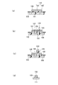
- (A)-(d) is sectional drawing which shows the manufacturing method of the electronic component which concerns on the 2nd Embodiment of this invention in the order of the process.
- the pressure-sensitive adhesive sheet of this embodiment has a configuration in which a pressure-sensitive adhesive layer is laminated on one surface of a base film, and a die attach film is further laminated on the pressure-sensitive adhesive layer. And the conductive filler is mix
- the pressure-sensitive adhesive constituting the pressure-sensitive adhesive layer contains (meth) acrylic acid ester copolymer: 100 parts by mass and polyfunctional isocyanate curing agent: 0.5-20 parts by mass, and (meth) acrylic acid.
- the copolymerization ratio of the monomer having a carboxyl group in the ester copolymer is less than 0.5%.
- the material of the base film is not particularly limited.
- the base film may be formed of a mixture or copolymer of these resins, or may be a laminate of films made of different materials.
- ionomer resins are preferable, and in particular, a copolymer having an ethylene unit, a (meth) acrylic acid unit, and a (meth) acrylic acid alkyl ester unit is used as Na + , K + , Zn 2+, or the like.
- An ionomer resin crosslinked with metal ions is preferred.
- such an ionomer resin is used for the base film, it is possible to suppress the generation of beard-like cutting waste during dicing.
- the base film is subjected to an antistatic treatment.
- the method of the antistatic treatment for the base film is not particularly limited. For example, (1) a treatment for adding an antistatic agent to the composition constituting the base film, and (2) a base film dia. A process of applying an antistatic agent to the surface on the touch film lamination side, (3) a charging process by corona discharge, or the like can be applied.
- a quaternary amine salt monomer or the like can be used as the antistatic agent.
- the quaternary amine salt monomer include dimethylaminoethyl (meth) acrylate quaternary chloride, diethylaminoethyl (meth) acrylate quaternary chloride, methylethylaminoethyl (meth) acrylate quaternary chloride, p- Examples include dimethylaminostyrene quaternary chloride and p-diethylaminostyrene quaternary chloride, and dimethylaminoethyl methacrylate quaternary chloride is particularly preferable.
- the pressure-sensitive adhesive constituting the pressure-sensitive adhesive layer is blended with a polyfunctional isocyanate curing agent with respect to 100 parts by mass of the (meth) acrylic acid ester copolymer.
- the (meth) acrylic acid ester copolymer has a copolymerization ratio of the monomer having a carboxyl group of less than 0.5%.
- the pressure-sensitive adhesive constituting the pressure-sensitive adhesive layer includes 20 to 200 parts by mass of a urethane acrylate oligomer having 4 or more vinyl groups, and 0.1 to 10 parts by mass of a silicone-modified acrylic resin in addition to the above-described components. It is preferable that it is blended.
- the (meth) acrylic acid ester copolymer contained in the pressure-sensitive adhesive layer of the pressure-sensitive adhesive sheet of this embodiment is a copolymer of (meth) acrylic acid ester as a main monomer and a vinyl compound monomer. is there.
- This (meth) acrylic acid ester copolymer is a photo-curing pressure-sensitive adhesive, and is three-dimensionally reticulated by irradiating with ultraviolet rays so that the die attach film can be easily peeled off.
- (meth) acrylic acid ester for example, butyl (meth) acrylate, 2-butyl (meth) acrylate, t-butyl (meth) acrylate, pentyl (meth) acrylate, octyl (meth) acrylate, 2 -Ethylhexyl (meth) acrylate, nonyl (meth) acrylate, decyl (meth) acrylate, lauryl (meth) acrylate, methyl (meth) acrylate, ethyl (meth) acrylate, isopropyl (meth) acrylate, tridecyl (meth) acrylate, myristyl (Meth) acrylate, cetyl (meth) acrylate, stearyl (meth) acrylate, cyclohexyl (meth) acrylate, isobornyl (meth) acrylate, dicyclopentanyl (meth) acrylate,
- Examples of the vinyl compound monomer include a functional group consisting of a hydroxyl group, a carboxyl group, an epoxy group, an amide group, an amino group, a methylol group, a sulfonic acid group, a sulfamic acid group, and a (phosphite) group.
- Monomers having one or more selected functional groups can be used.
- examples of the monomer having a hydroxyl group include 2-hydroxyethyl (meth) acrylate, 2-hydroxypropyl (meth) acrylate, 2-hydroxybutyl (meth) acrylate, and the like.
- Examples of the monomer having a carboxyl group include (meth) acrylic acid, crotonic acid, maleic acid, maleic anhydride, itaconic acid, fumaric acid, acrylamide N-glycolic acid and cinnamic acid.
- Examples of the monomer having an epoxy group include allyl glycidyl ether and (meth) acrylic acid glycidyl ether.
- Examples of the monomer having an amide group include (meth) acrylamide.
- Examples of the monomer having an amino group include N, N-dimethylaminoethyl (meth) acrylate.
- Examples of the monomer having a methylol group include N-methylol acrylamide.
- Examples of the method for producing the (meth) acrylic acid ester copolymer described above include emulsion polymerization and solution polymerization, and emulsion polymerization is preferred. Thereby, interaction with a die attach film can be suppressed and it becomes possible to peel a die attach film from an adhesive sheet easily.
- the polyfunctional isocyanate curing agent has two or more isocyanate groups, and examples thereof include aromatic polyisocyanates, aliphatic polyisocyanates, and alicyclic polyisocyanates.
- aromatic polyisocyanate for example, 1,3-phenylene diisocyanate, 4,4′-diphenyl diisocyanate, 1,4-phenylene diisocyanate, 4,4′-diphenylmethane diisocyanate, 2,4-tolylene diisocyanate, 2,4 , 6-tolylene diisocyanate, 4,4′-toluidine diisocyanate, 2,4,6-triisocyanate toluene, 1,3,5-triisocyanate benzene, dianisidine diisocyanate, 4,4′-diphenyl ether diisocyanate, 4,4 ', 4 "-triphenylmethane triisocyanate, ⁇ , ⁇ '-diisocyanate-1,3-dimethylbenzene, ⁇ , ⁇ '-diisocyanate-1,4-dimethylbenzene, ⁇ , ⁇ '-diisocyanate-1,4- Diechi Benzen
- aliphatic polyisocyanate examples include trimethylene diisocyanate, tetramethylene diisocyanate, hexamethylene diisocyanate, pentamethylene diisocyanate, 1,2-propylene diisocyanate, 2,3-butylene diisocyanate, 1,3-butylene diisocyanate, dodecamethylene diisocyanate and 2 4,4-trimethylhexamethylene diisocyanate and the like.
- Examples of the alicyclic polyisocyanate include 3-isocyanate methyl-3,5,5-trimethylcyclohexyl isocyanate, 1,3-cyclopentane diisocyanate, 1,3-cyclohexane diisocyanate, 1,4-cyclohexane diisocyanate, methyl-2, Examples include 4-cyclohexane diisocyanate, methyl-2,6-cyclohexane diisocyanate, 4,4′-methylenebis (cyclohexyl isocyanate), 1,4-bis (isocyanate methyl) cyclohexane, 1,4-bis (isocyanate methyl) cyclohexane, and the like. .
- 1,3-phenylene diisocyanate, 4,4′-diphenyl diisocyanate, 1,4-phenylene diisocyanate, 4,4′-diphenylmethane diisocyanate, 2,4-tolylene diisocyanate, 2,6 -Tolylene diisocyanate, 4,4'-toluidine diisocyanate and hexamethylene diisocyanate are preferred.
- the blending amount of the polyfunctional isocyanate curing agent is less than 0.5 parts by mass with respect to 100 parts by mass of the (meth) acrylic acid ester copolymer, the adhesive strength becomes too strong, resulting in pickup failure. .
- curing agent exceeds 20 mass parts with respect to 100 mass parts of (meth) acrylic acid ester copolymers, adhesive force will fall and it will be between an adhesive sheet and a ring frame at the time of dicing. The fixing force in between decreases. Therefore, in the pressure-sensitive adhesive sheet of this embodiment, the blending ratio of the polyfunctional isocyanate curing agent is 0.5 to 20 parts by mass with respect to 100 parts by mass of the (meth) acrylic acid ester copolymer.
- the blending ratio of the polyfunctional isocyanate curing agent is more preferably 1.0 to 10 parts by mass with respect to 100 parts by mass of the (meth) acrylic acid ester copolymer.
- urethane acrylate oligomer 20 to 200 parts by mass>
- a specific amount of urethane acrylate oligomer having four or more vinyl groups can be blended in the pressure-sensitive adhesive layer in order to make the die attach film easier to peel.
- the urethane acrylate oligomer having 4 or more vinyl groups (hereinafter also simply referred to as urethane acrylate oligomer) is a (meth) acrylate oligomer having 4 or more vinyl groups and having a urethane bond in the molecule. .
- the peelability of the die attach film from the adhesive layer cured by ultraviolet irradiation can be further improved.
- the semiconductor chip can be easily picked up with the die attach film attached.
- a urethane acrylate oligomer having less than 4 vinyl groups is blended in the adhesive layer, the adhesive strength after UV irradiation is insufficiently reduced, and the pickup characteristics are deteriorated.
- the blending amount is preferably 20 to 200 parts by mass with respect to 100 parts by mass of the (meth) acrylic acid ester copolymer.
- the compounding quantity of a urethane acrylate oligomer is less than 20 mass parts, the peelable improvement effect from the adhesion layer after ultraviolet irradiation is not fully acquired.
- the blending amount of the urethane acrylate oligomer exceeds 200 parts by mass, pick-up failure is likely to occur due to glue scraping during dicing, and minute adhesive residue due to reaction residues is likely to occur.
- adhesion failure during heating tends to occur.
- the urethane acrylate oligomer is produced by reacting (a) a (meth) acrylate compound having a hydroxyl group and a plurality of (meth) acrylate groups with a compound having a plurality of isocyanate groups (for example, a diisocyanate compound). (B) To a polyol oligomer having a plurality of hydroxyl ends, a compound having a plurality of isocyanate groups (for example, a diisocyanate compound) is added and reacted to form an oligomer having a plurality of isocyanate ends. Some have reacted with a (meth) acrylate compound having a (meth) acrylate group.
- examples of the (meth) acrylate compound having a hydroxyl group and a plurality of (meth) acrylate groups include hydroxypropylated trimethylolpropane triacrylate, pentaerythritol triacrylate, dipentaerythritol-hydroxy- Examples thereof include pentaacrylate, bis (pentaerythritol) -tetraacrylate, tetramethylolmethane-triacrylate, glycidol-diacrylate, and compounds having some or all of these acrylate groups as methacrylate groups.
- examples of the compound having a plurality of isocyanate groups include aromatic isocyanate, alicyclic isocyanate, and aliphatic isocyanate.
- aromatic diisocyanate examples include tolylene diisocyanate, 4,4-diphenylmethane diisocyanate, and xylylene diisocyanate.
- alicyclic diisocyanate examples include isophorone diisocyanate and methylene bis (4-cyclohexyl isocyanate).
- aliphatic diisocyanate examples include hexamethylene diisocyanate and trimethylhexamethylene diisocyanate.
- isocyanates aromatic isocyanates or alicyclic isocyanates having a plurality of isocyanate groups are preferred.
- isocyanate component there are a monomer, a dimer and a trimer, and a trimer is particularly preferable.
- examples of the polyol component of the polyol oligomer having a plurality of hydroxyl groups include poly (propylene oxide) diol, poly (propylene oxide) triol, copoly (ethylene oxide-propylene oxide) diol, poly ( Tetramethylene oxide) diol, ethoxylated bisphenol A, ethoxylated bisphenol S spiroglycol, caprolactone-modified diol, carbonate diol, and the like.
- ⁇ Silicone-modified acrylic resin 0.1 to 10 parts by mass>
- a specific amount of silicone-modified acrylic resin can be blended in the pressure-sensitive adhesive layer together with the urethane acrylate oligomer described above.
- a polymer of a (meth) acrylic monomer and a silicone-based macromonomer having a vinyl group at the end of the polydimethylsiloxane bond is preferable.
- a compound in which the terminal of the polydimethylsiloxane bond is a vinyl group such as a (meth) acryloyl group or a styryl group for the silicone-based macromonomer.
- the proportion of the silicone-based macromonomer unit in the silicone-modified acrylic resin is preferably 15 to 50 parts by mass per 100 parts by mass of the silicone-modified acrylic resin.
- a silicone-modified acrylic resin a silicone-modified acrylic resin having a structural unit derived from at least one of a reactive hydroxyalkyl (meth) acrylate, a modified hydroxy (meth) acrylate, and a monomer having a vinyl group Is preferably used.
- silicone-modified acrylic resins it is possible to prevent the occurrence of minute adhesive residue called particles when a semiconductor chip is picked up. Thereby, even when a die attach film is laminated on the adhesive layer, migration of the silicone-modified acrylic resin to the die attach film can be prevented.
- Examples of the (meth) acrylic monomer used as a raw material for the silicone-modified acrylic resin include alkyl (meth) acrylate, hydroxyalkyl (meth) acrylate, modified hydroxy (meth) acrylate, and (meth) acrylic acid.
- alkyl (meth) acrylate examples include methyl (meth) acrylate, ethyl (meth) acrylate, n-propyl (meth) acrylate, n-butyl (meth) acrylate, isobutyl (meth) acrylate, and t-butyl (meth) ) Acrylate, 2-ethylhexyl (meth) acrylate, lauryl (meth) acrylate, stearyl (meth) acrylate, isobornyl (meth) acrylate, and hydroxyalkyl (meth) acrylate.
- hydroxyalkyl (meth) acrylate examples include hydroxyethyl (meth) acrylate, hydroxypropyl (meth) acrylate, and hydroxybutyl (meth) acrylate.
- modified hydroxy (meth) acrylate examples include ethylene oxide-modified hydroxy (meth) acrylate and lactone-modified hydroxy (meth) acrylate.
- the blending amount is preferably 0.1 to 10 parts by mass with respect to 100 parts by mass of the (meth) acrylic acid ester polymer.
- the blending amount of the silicone-modified acrylic resin is less than 0.1 parts by mass, the effect of improving the peelability from the adhesive layer after ultraviolet irradiation cannot be obtained sufficiently.
- the compounding amount of the silicone-modified acrylic resin exceeds 10 parts by mass, the initial adhesive strength is greatly reduced, and peeling from the ring frame is likely to occur during dicing.
- the pressure-sensitive adhesive layer in the pressure-sensitive adhesive sheet of this embodiment contains additives such as a polymerization initiator, a softener, an anti-aging agent, a filler, an ultraviolet absorber, and a light stabilizer as long as other components are not affected. It may be.
- the thickness of the pressure-sensitive adhesive layer is less than 5 ⁇ m, the pressure-sensitive adhesive force is reduced, and the fixing force between the pressure-sensitive adhesive sheet and the ring frame may be reduced during dicing.
- the thickness of the adhesive layer exceeds 100 ⁇ m, the adhesive strength becomes too strong, and pickup failure may occur. Therefore, the thickness of the adhesive layer is preferably 5 to 100 ⁇ m. A more preferable range of the thickness of the pressure-sensitive adhesive layer is 20 to 50 ⁇ m, which can improve both the holding property and pick-up property of the semiconductor chip in a balanced manner.
- the die attach film used for the pressure-sensitive adhesive sheet of the present embodiment is obtained by molding an adhesive composition into a film and contains a conductive filler.
- the composition constituting the die attach film includes acrylic, polyamide, polyethylene, polysulfone, epoxy, polyimide, polyamide acid, silicone, phenol, rubber polymer, fluororubber polymer and fluorine. Examples thereof include a single resin, or a mixture or copolymer thereof.
- the die attach film may be a laminate of films made of different materials. Furthermore, a photopolymerization initiator, an antistatic agent, or a crosslinking accelerator may be added to the adhesive composition.
- the conductive filler is added to impart conductivity to the die attach film and improve heat dissipation.
- the conductive filler for example, silver, copper, boron nitride, alumina, gold, palladium, or nickel alone or a mixture thereof can be used. Note that silver, copper, boron nitride, or alumina is preferably used as the conductive filler from the viewpoint of reliability, heat dissipation characteristics, and cost.
- the blending amount of the conductive filler is preferably 10 to 1900 parts by mass with respect to 100 parts by mass of the resin component in the adhesive composition constituting the die attach film.
- the blending amount of the conductive filler is less than 10 parts by mass, the heat dissipation characteristics may be insufficient, and when the blending amount exceeds 1900 parts by mass, the film becomes brittle and the film forming property may be deteriorated. It is.
- the pressure-sensitive adhesive sheet of the present embodiment can also be produced by, for example, applying a pressure-sensitive adhesive on a base film to form a pressure-sensitive adhesive layer, and then attaching a separately formed die attach film on the pressure-sensitive adhesive layer. In that case, it is necessary to adjust the adhesive strength between the die attach film and the adhesive layer. If the adhesive strength between the die attach film and the adhesive layer is high, pick-up failure may occur. Conversely, if the adhesive strength is low, chip holding may be reduced. Specifically, the adhesive strength between the die attach film and the adhesive layer is preferably 0.05 to 0.9 N / 20 mm.
- the pressure-sensitive adhesive sheet of this embodiment includes a monomer having a carboxyl group in the (meth) acrylic acid ester copolymer contained in the pressure-sensitive adhesive layer while containing a conductive filler in the die attach film. Since the copolymerization ratio is less than 0.5%, conductivity can be imparted to the die attach film without deteriorating the retention and pick-up properties of the semiconductor chip.
- a fixing step is performed (step S1).
- a dicing process is performed in which the silicon wafer 101 is diced with the dicing blade 104 to form the semiconductor chip 108 (step S2).
- step S3 an expanding process is performed to expand the adhesive sheet 110 radially to widen the interval between the semiconductor chips 108 (step S3), and in this state, the semiconductor chip 108 is adsorbed and picked up by a vacuum collector (step S4).
- step S4 the semiconductor chip 108 is picked up with the die attach film 105 adhered and peeled between the adhesive layer 103 and the die attach film 105.
- step S5 a mounting process is performed in which the semiconductor chip 108 to which the die attach film 105 is attached is mounted on, for example, the lead frame 111 (step S5). Subsequently, the die attach film 105 is heated to heat and bond the semiconductor chip 108 and the lead frame 111 (step S6), and the semiconductor chip 108 mounted on the lead frame 111 or the circuit board is molded with resin (not shown). A molding step (step S7) is performed.
- both the holding property and pick-up property of the semiconductor chip are excellent in the manufacturing process.
- an adhesive having the composition shown in the following Tables 1 and 2 was applied onto a separator film made of polyethylene terephthalate, and coated so that the thickness of the adhesive layer after drying was 20 ⁇ m.
- the die attach film was cut into a 6.2-inch diameter circle and laminated on the adhesive layer to obtain each adhesive sheet of Examples and Comparative Examples. .
- an ionomer resin manufactured by Mitsui DuPont Polychemical Co., Ltd. was used as the base film in all of the Examples and Comparative Examples. Specifically, it is mainly composed of a Zn salt of an ethylene-methacrylic acid-methacrylic acid alkyl ester copolymer, contains Zn 2+ ions, and has an MFR (melt flow rate) value of 1.5 g / 10 min. (JIS K7210, 210 ° C.), melting point is 96 ° C., thickness is 80 ⁇ m.
- each component contained in the adhesive layer is as follows.
- ⁇ Multifunctional isocyanate curing agent> A Coronate L-45E (registered trademark) manufactured by Nippon Polyurethane Trimethylolpropane adduct of 2,4-tolylene diisocyanate
- ⁇ Silicone-modified acrylic resin> A: UTMM-LS2 manufactured by Soken Chemical Co., Ltd.
- a silicone-based graft copolymer comprising a silicone-based oligomer unit having a (meth) acryloyl group at the end of a silicone molecular chain and polymerizing an acrylic vinyl unit composed of methyl methacrylate or the like.
- Photopolymerization initiator benzyldimethyl ketal, specifically, Irgacure 651 (registered trademark) manufactured by Ciba Specialty Chemicals was used.
- Step S1 An attaching step of attaching and fixing the silicon wafer 101 to the adhesive sheet 110 and an attaching step of fixing the adhesive sheet 110 to the ring frame 102 were performed simultaneously (see FIG. 1A). At that time, a silicon wafer having a diameter of 8 inches and a thickness of 0.3 mm on which a dummy circuit pattern was formed was used as the silicon wafer 101.
- Step S2 A dicing process was performed with the dicing blade 104 to turn the silicon wafer 101 into a semiconductor chip 108 having a chip size of 6 mm ⁇ 6 mm (see FIG. 1B).
- the main settings for dicing are as follows.
- Dicing blade feed rate 50 mm / sec
- Cutting water temperature 25 ° C.
- Cutting water volume 1.0L / min
- Step S3 The expanding process which expanded the space
- the amount of expansion at this time was 8 mm.
- Step S4 After being pushed up by a needle pin (not shown), the semiconductor chip 108 is adsorbed by a vacuum collector (not shown), peeled between the adhesive layer 103 and the die attach film 105, and the die attach film 105 is adhered. A pickup process for picking up the chip 108 was performed (see FIG. 1C). The main settings for the pickup are as follows. Pickup device: CAP-300II manufactured by Canon Machinery Needle pin shape: 250 ⁇ mR Needle pin push-up height: 0.5mm
- Step S5 A mounting step of mounting the semiconductor chip 108 to which the die attach film 105 was attached on the lead frame 111 was performed (see FIG. 1D).
- Step S6 The die attach film 105 was heated, and a heat bonding step for heat bonding the semiconductor chip 108 and the lead frame 111 was performed (not shown).
- Step S7 A molding process for molding the semiconductor chip 108 mounted on the lead frame 111 with a resin (not shown) was performed (not shown).
- Chip retention and pick-up performance were evaluated based on the following criteria.
- Chip retention> The chip retainability was evaluated by the remaining rate of the semiconductor chip 108 in which the semiconductor chip 108 is held on the adhesive sheet 110 after the dicing process in step S3.
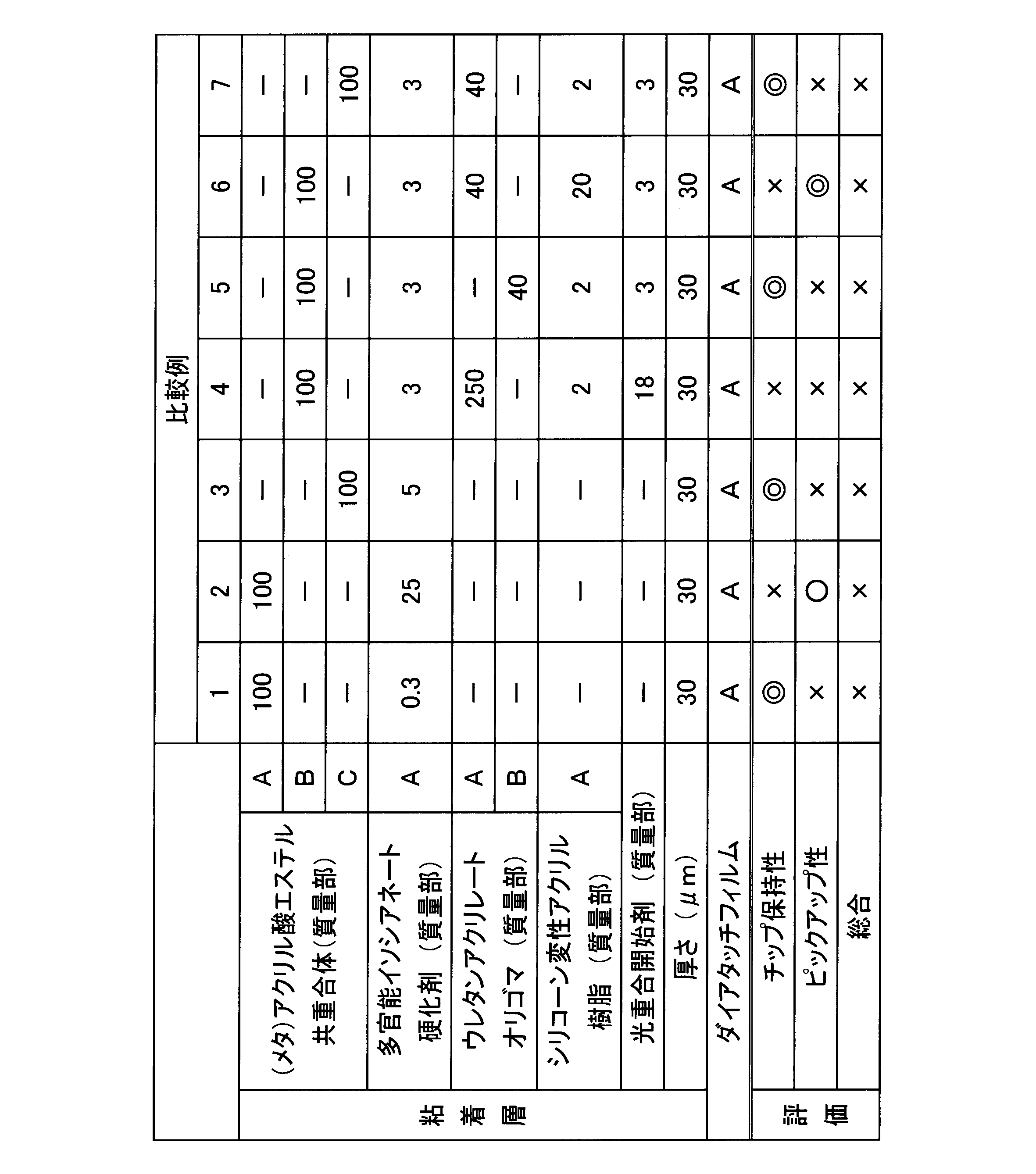
- the pressure-sensitive adhesive sheets of Comparative Example 3 and Comparative Example 7 using a (meth) acrylic acid ester copolymer in which the copolymerization ratio of the monomer having a carboxyl group is 0.5% or more have both pickup properties. It was inferior.
- the pressure-sensitive adhesive sheet of Comparative Example 4 to which an amount of urethane acrylate oligomer exceeding 200 parts by mass was inferior in both chip retention and pickup properties.
- the pressure-sensitive adhesive sheet of Comparative Example 5 to which a urethane acrylate oligomer having less than 4 vinyl groups was added had poor pick-up properties. Furthermore, the pressure-sensitive adhesive sheet of Comparative Example 6 to which an amount of silicone-modified acrylic resin exceeding 10 parts by mass was inferior in chip retention.
- the pressure-sensitive adhesive sheets of Examples 1 to 13 produced within the scope of the present invention were excellent in both chip retention and pick-up properties. Thereby, according to this invention, it was confirmed that the die attach film has electroconductivity, and the adhesive sheet which is excellent also in the retention property and pick-up property of a semiconductor chip is obtained.
Landscapes
- Chemical & Material Sciences (AREA)
- Organic Chemistry (AREA)
- Health & Medical Sciences (AREA)
- Chemical Kinetics & Catalysis (AREA)
- Medicinal Chemistry (AREA)
- Polymers & Plastics (AREA)
- Adhesive Tapes (AREA)
- Adhesives Or Adhesive Processes (AREA)
- Die Bonding (AREA)
Abstract
Description
この粘着シートでは、前記粘着層が、更に、ビニル基を4個以上有するウレタンアクリレートオリゴマ:20~200質量部と、シリコーン変性アクリル樹脂:0.1~10質量部と、を含有していてもよい。
また、前記粘着層の厚さは、例えば20~50μmとすることができる。
更に、前記導電性フィラーとしては、例えば銀、銅、窒化ホウ素又はアルミナの単体若しくは混合体を使用することができる。
ここで、単量体単位とは単量体に由来する構造単位を意味する。「部」及び「%」は質量基準である。(メタ)アクリレートとはアクリレート及びメタアクリレートの総称である。(メタ)アクリル酸等の(メタ)を含む化合物等も同様に、名称中に「メタ」を有する化合物と「メタ」を有さない化合物の総称である。
先ず、本発明の第1の実施形態に係る粘着シートについて説明する。本実施形態の粘着シートは、基材フィルムの一方の面に粘着層が積層され、この粘着層に更にダイアタッチフィルムが積層された構成となっている。そして、ダイアタッチフィルムには、導電性フィラーが配合されている。また、粘着層を構成する粘着剤は、(メタ)アクリル酸エステル共重合体:100質量部と、多官能イソシアネート硬化剤:0.5~20質量部とを含有し、かつ(メタ)アクリル酸エステル共重合体におけるカルボキシル基を有する単量体の共重合比率が0.5%未満である。
基材フィルムの材質は特に限定されるものではないが、例えばポリ塩化ビニル、ポリエチレンテレフタレート、エチレン-酢酸ビニル共重合体、エチレン-アクリル酸-アクリル酸エステル、エチレン-エチルアクリレート共重合体、ポリエチレン、ポリプロピレン、エチレン-アクリル酸共重合体、又は、エチレン-(メタ)アクリル酸共重合体やエチレン-(メタ)アクリル酸-(メタ)アクリル酸エステル共重合体等を金属イオンで架橋したアイオノマ樹脂等で形成することができる。なお、基材フィルムは、これらの樹脂の混合物又は共重合体で形成されていてもよく、また材質が異なるフィルムを積層したものでもよい。
粘着層を構成する粘着剤は、(メタ)アクリル酸エステル共重合体100質量部に対して、多官能イソシアネート硬化剤を配合されている。また、(メタ)アクリル酸エステル共重合体は、カルボキシル基を有する単量体の共重合比率が0.5%未満である。更に、粘着層を構成する粘着剤には、前述した各成分に加えて、ビニル基を4個以上有するウレタンアクリレートオリゴマが20~200質量部、及びシリコーン変性アクリル樹脂が0.1~10質量部配合されていることが好ましい。
本実施形態の粘着シートの粘着層に含有される(メタ)アクリル酸エステル共重合体は、主単量体である(メタ)アクリル酸エステルと、ビニル化合物単量体とを共重合したものである。この(メタ)アクリル酸エステル共重合体は、光硬化型の感圧性粘着剤であり、紫外線を照射することにより三次元網状化し、ダイアタッチフィルムを容易に剥離できるようになる。
多官能イソシアネート硬化剤は、イソシアネート基を2個以上有するものであり、例えば芳香族ポリイソシアネート、脂肪族ポリイソシアネート及び脂環族ポリイソシアネート等がある。
本実施形態の粘着シートでは、ダイアタッチフィルムをより剥離しやすくするため、粘着層に、ビニル基を4個以上有するウレタンアクリレートオリゴマを、特定量配合することができる。ここで、ビニル基を4個以上有するウレタンアクリレートオリゴマ(以下、単にウレタンアクリレートオリゴマともいう。)とは、ビニル基を4個以上有し、分子内にウレタン結合を有する(メタ)アクリレートオリゴマである。
本実施形態の粘着シートでは、ダイアタッチフィルムをより剥離しやすくするために、粘着層に、前述したウレタンアクリレートオリゴマと共に、シリコーン変性アクリル樹脂を、特定量配合することができる。
本実施形態の粘着シートにおける粘着層は、他の成分に影響を与えない範囲で、重合開始剤、軟化剤、老化防止剤、充填剤、紫外線吸収剤及び光安定剤等の添加剤を含有していてもよい。
粘着層の厚さが5μm未満の場合、粘着力が低下してダイシング時に粘着シートとリングフレームとの間の固定力が低下することがある。また、粘着層の厚さが100μmを超えると、粘着力が強くなりすぎて、ピックアップ不良が発生することがある。よって、粘着層の厚さは、5~100μmであることが好ましい。なお、粘着層の厚さのより好ましい範囲は、20~50μmであり、これにより、半導体チップの保持性とピックアップ性の両方を、バランスよく向上させることができる。
本実施形態の粘着シートに用いられるダイアタッチフィルムは、接着剤組成物をフィルム状に成形したものであり、導電性フィラーを含有している。このダイアタッチフィルムを構成する組成物としては、アクリル系、ポリアミド系、ポリエチレン系、ポリスルホン系、エポキシ系、ポリイミド系、ポリアミド酸系、シリコーン系、フェノール系、ゴム系ポリマー、フッ素ゴム系ポリマー及びフッ素樹脂の単体、又はこれらの混合物若しくは共重合体等が挙げられる。また、ダイアタッチフィルムは、材質の異なるフィルムを積層したものでもよい。更に、接着剤組成物には、光重合開始剤、帯電防止剤又は架橋促進剤が添加されていてもよい。
一方、導電性フィラーは、ダイアタッチフィルムに導電性を付与すると共に、放熱性を向上させるために配合されている。この導電性フィラーとしては、例えば銀、銅、窒化ホウ素、アルミナ、金、パラジウム又はニッケルの単体若しくは混合体を使用することができる。なお、信頼性、放熱特性及びコストの面から、導電性フィラーには、銀、銅、窒化ホウ素又はアルミナを使用することが好ましい。
次に、本発明の第2の実施形態に係る電子部品について説明する。本実施形態の電子部品は、前述した第1の実施形態の粘着シートを使用して、半導体チップ等が実装されている。図1(a)~(d)は本実施形態の電子部品の製造方法を、その工程順に示す断面図である。

A:綜研化学社製 SKダイン1496
2-エチルヘキシルアクリレート:95質量%と、2-ヒドロキシエチルアクリレート:5質量%とを、溶液重合して得た共重合体。カルボキシル基なし。
B:日本ゼオン社製 AR53L
エチルアクリレート:40質量%と、ブチルアクリレート:23質量%と、メトキシエチルアクリレート:37質量%とを、懸濁重合して得た共重合体。カルボキシル基なし。
C:綜研化学社製 SKダイン1305H
ブチルアクリレート:65質量%、メチルアクリレート:25質量%、アクリル酸:5質量%の共重合体、溶液重合により得られる。カルボキシル基あり(単量体の共重合比率:5%)。
A:日本ポリウレタン社製 コロネートL-45E(登録商標)
2,4-トリレンジイソシアネートのトリメチロールプロパンアダクト体
上記表1及び表2においては、単に、ウレタンアクリレートオリゴマと記載している。
A:根上工業社製 UN-3320HS
イソホロンジイソシアネート(脂環族ジイソシアネート)の三量体を反応させた末端イソシアネートオリゴマに、ジペタエリスリトールペンタアクリレートを反応させた末端アクリレートオリゴマ。数平均分子量3700。アクリレート官能基数15個。
B:新中村化学社製 UA-340P
ポリ(プロピレングリコール)ジオールの末端にイソホロンジイソシアネートを反応させてなる末端イソシアネートオリゴマに、更に2-ヒドロキシエチルアクリレートを反応させてなる末端アクリレートオリゴマ。数平均分子量13000。ビニル基数1分子あたり2個。
A:綜研化学社製 UTMM-LS2
シリコーン分子鎖の末端に(メタ)アクリロイル基を有するシリコーン系オリゴマ系単位を含有し、メチルメタアクリレート等からなるアクリルビニル単位を重合したシリコーン系グラフト共重合体。
A:エポキシ接着剤を主体とする樹脂成分100質量部に対して、銀フィラーを400質量部含有。厚さ30μm。
B:エポキシ接着剤を主体とする樹脂成分100質量部に対して、窒化ホウ素フィラーを400質量部含有。厚さ30μm。
C:エポキシ接着剤を主体とする樹脂成分100質量部に対して、アルミナフィラーを400質量部含有。厚さ30μm。
D:エポキシ接着剤を主体とする樹脂成分100質量部に対して、ニッケルフィラーを400質量部含有。厚さ30μm。
光重合開始剤は、ベンジルジメチルケタール、具体的には、チバスペシャリティーケミカルズ社製 イルガキュア651(登録商標)を用いた。
シリコンウエハ101を、粘着シート110に貼り付けて固定する貼付工程と、粘着シート110をリングフレーム102に固定する固定工程とを同時に行った(図1(a)参照)。その際、シリコンウエハ101には、ダミーの回路パターンを形成した直径8インチ×厚さ0.3mmのシリコンウエハを用いた。
ダイシングブレード104で、シリコンウエハ101を、6mm×6mmのチップサイズの半導体チップ108にするダイシング工程を行った(図1(b)参照)。ダイシングにおける主な設定は、以下の通りである。
粘着シート110への切り込み107の量:15μm
ダイシング装置:DISCO社製 DAD341
ダイシングブレード:DISCO社製 NBC-ZH205O-27HEEE
ダイシングブレード形状:外径55.56mm、刃幅35μm、内径19.05mm
ダイシングブレード回転数:40,000rpm
ダイシングブレード送り速度:50mm/秒
切削水温度:25℃
切削水量:1.0L/分
粘着シート110を放射状に拡大して、半導体チップ108の間隔を広げるエキスパンド工程を行った(図示せず)。このときのエキスパンド量は、8mmとした。
ニードルピン(図示せず)で突き上げた後、真空コレツト(図示せず)で半導体チップ108を吸着し、粘着層103とダイアタッチフィルム105との間で剥離し、ダイアタッチフィルム105が付着した半導体チップ108をピックアップするピックアップ工程を行った(図1(c)参照)。ピックアップにおける主な設定は、以下の通りである。
ピックアップ装置:キヤノンマシナリー社製 CAP-300II
ニードルピン形状:250μmR
ニードルピン突き上げ高さ:0.5mm
ダイアタッチフィルム105が付着した半導体チップ108を、リードフレーム111上に搭載する搭載工程を行った(図1(d)参照)。
ダイアタッチフィルム105を加熱し、半導体チップ108とリードフレーム111とを加熱接着する加熱接着工程を行った(図示せず)。
リードフレーム111に搭載した半導体チップ108を、樹脂(図示せず)でモールドするモールド工程を行った(図示せず)。
チップ保持性は、ステップS3のダイシング工程後において、半導体チップ108が粘着シート110に保持されている半導体チップ108の残存率で評価した。
◎(優):チップ飛びが5%未満。
○(良):チップ飛びが5%以上10%未満。
×(不可):チップ飛びが10%以上。
ピックアップ性は、ステップS5のピックアップ工程において、ピックアップできた率で評価した。
◎(優):95%以上のチップがピックアップできた。
○(良):80%以上95%未満のチップがピックアップできた。
×(不可):80%未満のチップがピックアップできた。
102 リングフレーム
103 粘着層
104 ダイシングブレード
107 切り込み
105 ダイアタッチフィルム
106 基材フィルム
108 半導体チップ
110 粘着シート
111 リードフレーム
Claims (5)
- 基材フィルムと、
該基材フィルムの一方の面に積層された粘着層と、
該粘着層に積層され、導電性フィラーを含有するダイアタッチフィルムと、を備え、
前記粘着層は、
カルボキシル基を有する単量体の共重合比率が0.5%未満である(メタ)アクリル酸エステル共重合体:100質量部と、
多官能イソシアネート硬化剤:0.5~20質量部と、
を含有する粘着シート。 - 前記粘着層は、更に、
ビニル基を4個以上有するウレタンアクリレートオリゴマ:20~200質量部と、
シリコーン変性アクリル樹脂:0.1~10質量部と、
を含有する請求項1に記載の粘着シート。 - 前記粘着層の厚さが、20~50μmである請求項1又は2に記載の粘着シート。
- 前記導電性フィラーが、銀、銅、窒化ホウ素又はアルミナの単体若しくは混合体である請求項1乃至3のいずれか1項記載の粘着シート。
- 請求項1乃至4のいずれか1項に記載の粘着シートを用いて製造された電子部品。
Priority Applications (4)
| Application Number | Priority Date | Filing Date | Title |
|---|---|---|---|
| JP2011543214A JPWO2011065252A1 (ja) | 2009-11-30 | 2010-11-16 | 粘着シート及び電子部品 |
| CN2010800541765A CN102640277A (zh) | 2009-11-30 | 2010-11-16 | 粘合片及电子部件 |
| PH1/2012/501010A PH12012501010A1 (en) | 2009-11-30 | 2010-11-16 | Adhesive sheet and electronic component |
| US13/510,821 US20120231266A1 (en) | 2009-11-30 | 2010-11-16 | Adhesive sheet and electronic component |
Applications Claiming Priority (2)
| Application Number | Priority Date | Filing Date | Title |
|---|---|---|---|
| JP2009-271023 | 2009-11-30 | ||
| JP2009271023 | 2009-11-30 |
Publications (1)
| Publication Number | Publication Date |
|---|---|
| WO2011065252A1 true WO2011065252A1 (ja) | 2011-06-03 |
Family
ID=44066357
Family Applications (1)
| Application Number | Title | Priority Date | Filing Date |
|---|---|---|---|
| PCT/JP2010/070348 Ceased WO2011065252A1 (ja) | 2009-11-30 | 2010-11-16 | 粘着シート及び電子部品 |
Country Status (8)
| Country | Link |
|---|---|
| US (1) | US20120231266A1 (ja) |
| JP (1) | JPWO2011065252A1 (ja) |
| KR (1) | KR20120099238A (ja) |
| CN (1) | CN102640277A (ja) |
| PH (1) | PH12012501010A1 (ja) |
| SG (1) | SG10201407993YA (ja) |
| TW (1) | TWI500728B (ja) |
| WO (1) | WO2011065252A1 (ja) |
Cited By (9)
| Publication number | Priority date | Publication date | Assignee | Title |
|---|---|---|---|---|
| JP2013028733A (ja) * | 2011-07-29 | 2013-02-07 | Sumitomo Bakelite Co Ltd | 液状樹脂組成物および半導体装置 |
| JP2014104705A (ja) * | 2012-11-29 | 2014-06-09 | Toppan Printing Co Ltd | 転写フィルム |
| JP2015098095A (ja) * | 2013-11-18 | 2015-05-28 | 凸版印刷株式会社 | インモールド成形用転写フィルム及びそれを用いた成形品 |
| JPWO2013141251A1 (ja) * | 2012-03-23 | 2015-08-03 | リンテック株式会社 | フィルム、ワーク加工用シート基材およびワーク加工用シート |
| JP2015158633A (ja) * | 2014-02-25 | 2015-09-03 | 株式会社リコー | クリーニングブレード、画像形成装置、及びプロセスカートリッジ |
| JP2017504976A (ja) * | 2013-12-13 | 2017-02-09 | エルジー・ケム・リミテッド | ダイシングフィルム粘着層形成用組成物およびダイシングフィルム |
| JP2017505716A (ja) * | 2014-01-20 | 2017-02-23 | テーザ・ソシエタス・ヨーロピア | 平坦形成物から浸透物を除去する方法 |
| JP2017509768A (ja) * | 2013-12-19 | 2017-04-06 | エルジー・ケム・リミテッド | ダイシングフィルム粘着層形成用組成物およびダイシングフィルム |
| JP2017100366A (ja) * | 2015-12-02 | 2017-06-08 | 三菱ケミカル株式会社 | 樹脂積層体及びその製造方法 |
Families Citing this family (12)
| Publication number | Priority date | Publication date | Assignee | Title |
|---|---|---|---|---|
| KR101628435B1 (ko) * | 2013-01-21 | 2016-06-08 | 제일모직주식회사 | 점착 필름, 이를 위한 점착제 조성물 및 이를 포함하는 디스플레이 부재 |
| TWI591151B (zh) | 2013-05-24 | 2017-07-11 | 明基材料股份有限公司 | 一種用於電子元件間電性導通的黏著劑 |
| CN103360956B (zh) * | 2013-06-18 | 2015-06-03 | 明基材料有限公司 | 一种用于电子元件间电性导通的粘着剂 |
| WO2015088282A1 (ko) * | 2013-12-13 | 2015-06-18 | 주식회사 엘지화학 | 다이싱 필름 점착층 형성용 조성물 및 다이싱 필름 |
| WO2015093794A1 (ko) * | 2013-12-19 | 2015-06-25 | 주식회사 엘지화학 | 다이싱 필름 점착층 형성용 조성물 및 다이싱 필름 |
| JP6334223B2 (ja) * | 2014-03-26 | 2018-05-30 | リンテック株式会社 | 粘着シート |
| KR102430472B1 (ko) * | 2014-12-25 | 2022-08-05 | 덴카 주식회사 | 레이저 다이싱용 점착 시트 및 반도체 장치의 제조 방법 |
| JP6557510B2 (ja) * | 2015-05-08 | 2019-08-07 | 積水化学工業株式会社 | 導電性粘着テープ及び導電性粘着剤組成物 |
| JP6429824B2 (ja) * | 2016-03-31 | 2018-11-28 | 古河電気工業株式会社 | 電子デバイスパッケージ用テープ |
| TWI811497B (zh) * | 2018-12-05 | 2023-08-11 | 南韓商Lg化學股份有限公司 | 黏著劑組成物、表面保護膜及用於製造有機發光電子裝置之方法 |
| JP7490399B2 (ja) * | 2020-03-13 | 2024-05-27 | 日東電工株式会社 | 再剥離粘着テープ |
| CN112300708B (zh) * | 2020-11-04 | 2022-09-30 | 深圳广恒威科技有限公司 | 可uv固化的胶膜及其应用 |
Citations (3)
| Publication number | Priority date | Publication date | Assignee | Title |
|---|---|---|---|---|
| JP2006210433A (ja) * | 2005-01-25 | 2006-08-10 | Sekisui Chem Co Ltd | ウエハ貼着用粘着シート及び半導体の製造方法 |
| WO2009050786A1 (ja) * | 2007-10-16 | 2009-04-23 | Denki Kagaku Kogyo Kabushiki Kaisha | 粘着剤、粘着シート、多層粘着シート及び電子部品の製造方法 |
| WO2009078203A1 (ja) * | 2007-12-19 | 2009-06-25 | Denki Kagaku Kogyo Kabushiki Kaisha | 多層粘着シート及び多層粘着シートを用いた電子部品の製造方法 |
Family Cites Families (2)
| Publication number | Priority date | Publication date | Assignee | Title |
|---|---|---|---|---|
| JP4275522B2 (ja) * | 2003-12-26 | 2009-06-10 | 日東電工株式会社 | ダイシング・ダイボンドフィルム |
| WO2009050785A1 (ja) * | 2007-10-16 | 2009-04-23 | Denki Kagaku Kogyo Kabushiki Kaisha | 粘着剤、粘着シート、多層粘着シート及び電子部品の製造方法 |
-
2010
- 2010-11-16 WO PCT/JP2010/070348 patent/WO2011065252A1/ja not_active Ceased
- 2010-11-16 PH PH1/2012/501010A patent/PH12012501010A1/en unknown
- 2010-11-16 SG SG10201407993YA patent/SG10201407993YA/en unknown
- 2010-11-16 KR KR20127013378A patent/KR20120099238A/ko not_active Ceased
- 2010-11-16 US US13/510,821 patent/US20120231266A1/en not_active Abandoned
- 2010-11-16 JP JP2011543214A patent/JPWO2011065252A1/ja active Pending
- 2010-11-16 CN CN2010800541765A patent/CN102640277A/zh active Pending
- 2010-11-26 TW TW099141078A patent/TWI500728B/zh active
Patent Citations (3)
| Publication number | Priority date | Publication date | Assignee | Title |
|---|---|---|---|---|
| JP2006210433A (ja) * | 2005-01-25 | 2006-08-10 | Sekisui Chem Co Ltd | ウエハ貼着用粘着シート及び半導体の製造方法 |
| WO2009050786A1 (ja) * | 2007-10-16 | 2009-04-23 | Denki Kagaku Kogyo Kabushiki Kaisha | 粘着剤、粘着シート、多層粘着シート及び電子部品の製造方法 |
| WO2009078203A1 (ja) * | 2007-12-19 | 2009-06-25 | Denki Kagaku Kogyo Kabushiki Kaisha | 多層粘着シート及び多層粘着シートを用いた電子部品の製造方法 |
Cited By (10)
| Publication number | Priority date | Publication date | Assignee | Title |
|---|---|---|---|---|
| JP2013028733A (ja) * | 2011-07-29 | 2013-02-07 | Sumitomo Bakelite Co Ltd | 液状樹脂組成物および半導体装置 |
| JPWO2013141251A1 (ja) * | 2012-03-23 | 2015-08-03 | リンテック株式会社 | フィルム、ワーク加工用シート基材およびワーク加工用シート |
| JP2014104705A (ja) * | 2012-11-29 | 2014-06-09 | Toppan Printing Co Ltd | 転写フィルム |
| JP2015098095A (ja) * | 2013-11-18 | 2015-05-28 | 凸版印刷株式会社 | インモールド成形用転写フィルム及びそれを用いた成形品 |
| JP2017504976A (ja) * | 2013-12-13 | 2017-02-09 | エルジー・ケム・リミテッド | ダイシングフィルム粘着層形成用組成物およびダイシングフィルム |
| JP2017509768A (ja) * | 2013-12-19 | 2017-04-06 | エルジー・ケム・リミテッド | ダイシングフィルム粘着層形成用組成物およびダイシングフィルム |
| US10526513B2 (en) | 2013-12-19 | 2020-01-07 | Lg Chem, Ltd. | Composition for forming adhesive layer of dicing film, and dicing film |
| JP2017505716A (ja) * | 2014-01-20 | 2017-02-23 | テーザ・ソシエタス・ヨーロピア | 平坦形成物から浸透物を除去する方法 |
| JP2015158633A (ja) * | 2014-02-25 | 2015-09-03 | 株式会社リコー | クリーニングブレード、画像形成装置、及びプロセスカートリッジ |
| JP2017100366A (ja) * | 2015-12-02 | 2017-06-08 | 三菱ケミカル株式会社 | 樹脂積層体及びその製造方法 |
Also Published As
| Publication number | Publication date |
|---|---|
| SG10201407993YA (en) | 2015-01-29 |
| TWI500728B (zh) | 2015-09-21 |
| CN102640277A (zh) | 2012-08-15 |
| US20120231266A1 (en) | 2012-09-13 |
| PH12012501010A1 (en) | 2017-08-23 |
| TW201129670A (en) | 2011-09-01 |
| KR20120099238A (ko) | 2012-09-07 |
| JPWO2011065252A1 (ja) | 2013-04-11 |
Similar Documents
| Publication | Publication Date | Title |
|---|---|---|
| WO2011065252A1 (ja) | 粘着シート及び電子部品 | |
| CN102971839B (zh) | 多层粘合片及电子元件的制造方法 | |
| JP5618994B2 (ja) | 粘着剤、粘着シート及び電子部品の製造方法 | |
| KR101359748B1 (ko) | 점착제, 점착 시트, 다층 점착 시트 및 전자 부품의 제조 방법 | |
| KR101784191B1 (ko) | 전자부품의 제조방법 | |
| JP5161284B2 (ja) | 電子部品の製造方法 | |
| CN110272696A (zh) | 背面研磨用粘着胶带 | |
| WO2016175112A1 (ja) | ワーク加工用粘着テープ | |
| KR101559190B1 (ko) | 다이싱 방법 | |
| JP5210346B2 (ja) | 粘着シート及び電子部品の製造方法 | |
| JP5890405B2 (ja) | 粘着シートおよび電子部品の製造方法 | |
| JP2011044444A (ja) | 多層粘着シート及び多層粘着シートを用いた電子部品の製造方法。 | |
| JP5468523B2 (ja) | 粘着剤、粘着シート及び電子部品の製造方法。 | |
| KR20230159372A (ko) | 반도체 가공용 점착 테이프 및 반도체 장치의 제조방법 | |
| JP5016703B2 (ja) | 粘着シート及び電子部品の製造方法 | |
| TW202525583A (zh) | 晶圓背面研磨用粘結膜 | |
| KR20230159373A (ko) | 반도체 가공용 점착 테이프 및 반도체 장치의 제조방법 | |
| KR20230160228A (ko) | 반도체 가공용 점착 테이프 및 반도체 장치의 제조방법 |
Legal Events
| Date | Code | Title | Description |
|---|---|---|---|
| WWE | Wipo information: entry into national phase |
Ref document number: 201080054176.5 Country of ref document: CN |
|
| 121 | Ep: the epo has been informed by wipo that ep was designated in this application |
Ref document number: 10833099 Country of ref document: EP Kind code of ref document: A1 |
|
| WWE | Wipo information: entry into national phase |
Ref document number: 2011543214 Country of ref document: JP |
|
| WWE | Wipo information: entry into national phase |
Ref document number: 13510821 Country of ref document: US |
|
| WWE | Wipo information: entry into national phase |
Ref document number: 12012501010 Country of ref document: PH |
|
| ENP | Entry into the national phase |
Ref document number: 20127013378 Country of ref document: KR Kind code of ref document: A |
|
| NENP | Non-entry into the national phase |
Ref country code: DE |
|
| 122 | Ep: pct application non-entry in european phase |
Ref document number: 10833099 Country of ref document: EP Kind code of ref document: A1 |