WO2011062046A1 - 液晶表示装置および液晶表示装置の製造方法 - Google Patents
液晶表示装置および液晶表示装置の製造方法 Download PDFInfo
- Publication number
- WO2011062046A1 WO2011062046A1 PCT/JP2010/069307 JP2010069307W WO2011062046A1 WO 2011062046 A1 WO2011062046 A1 WO 2011062046A1 JP 2010069307 W JP2010069307 W JP 2010069307W WO 2011062046 A1 WO2011062046 A1 WO 2011062046A1
- Authority
- WO
- WIPO (PCT)
- Prior art keywords
- transparent conductive
- conductive film
- film
- liquid crystal
- crystal display
- Prior art date
- Legal status (The legal status is an assumption and is not a legal conclusion. Google has not performed a legal analysis and makes no representation as to the accuracy of the status listed.)
- Ceased
Links
Images










Classifications
-
- G—PHYSICS
- G02—OPTICS
- G02F—OPTICAL DEVICES OR ARRANGEMENTS FOR THE CONTROL OF LIGHT BY MODIFICATION OF THE OPTICAL PROPERTIES OF THE MEDIA OF THE ELEMENTS INVOLVED THEREIN; NON-LINEAR OPTICS; FREQUENCY-CHANGING OF LIGHT; OPTICAL LOGIC ELEMENTS; OPTICAL ANALOGUE/DIGITAL CONVERTERS
- G02F1/00—Devices or arrangements for the control of the intensity, colour, phase, polarisation or direction of light arriving from an independent light source, e.g. switching, gating or modulating; Non-linear optics
- G02F1/01—Devices or arrangements for the control of the intensity, colour, phase, polarisation or direction of light arriving from an independent light source, e.g. switching, gating or modulating; Non-linear optics for the control of the intensity, phase, polarisation or colour
- G02F1/13—Devices or arrangements for the control of the intensity, colour, phase, polarisation or direction of light arriving from an independent light source, e.g. switching, gating or modulating; Non-linear optics for the control of the intensity, phase, polarisation or colour based on liquid crystals, e.g. single liquid crystal display cells
- G02F1/133—Constructional arrangements; Operation of liquid crystal cells; Circuit arrangements
- G02F1/1333—Constructional arrangements; Manufacturing methods
- G02F1/1343—Electrodes
- G02F1/134309—Electrodes characterised by their geometrical arrangement
-
- G—PHYSICS
- G02—OPTICS
- G02F—OPTICAL DEVICES OR ARRANGEMENTS FOR THE CONTROL OF LIGHT BY MODIFICATION OF THE OPTICAL PROPERTIES OF THE MEDIA OF THE ELEMENTS INVOLVED THEREIN; NON-LINEAR OPTICS; FREQUENCY-CHANGING OF LIGHT; OPTICAL LOGIC ELEMENTS; OPTICAL ANALOGUE/DIGITAL CONVERTERS
- G02F1/00—Devices or arrangements for the control of the intensity, colour, phase, polarisation or direction of light arriving from an independent light source, e.g. switching, gating or modulating; Non-linear optics
- G02F1/01—Devices or arrangements for the control of the intensity, colour, phase, polarisation or direction of light arriving from an independent light source, e.g. switching, gating or modulating; Non-linear optics for the control of the intensity, phase, polarisation or colour
- G02F1/13—Devices or arrangements for the control of the intensity, colour, phase, polarisation or direction of light arriving from an independent light source, e.g. switching, gating or modulating; Non-linear optics for the control of the intensity, phase, polarisation or colour based on liquid crystals, e.g. single liquid crystal display cells
- G02F1/133—Constructional arrangements; Operation of liquid crystal cells; Circuit arrangements
- G02F1/1333—Constructional arrangements; Manufacturing methods
- G02F1/1345—Conductors connecting electrodes to cell terminals
- G02F1/13452—Conductors connecting driver circuitry and terminals of panels
-
- G—PHYSICS
- G02—OPTICS
- G02F—OPTICAL DEVICES OR ARRANGEMENTS FOR THE CONTROL OF LIGHT BY MODIFICATION OF THE OPTICAL PROPERTIES OF THE MEDIA OF THE ELEMENTS INVOLVED THEREIN; NON-LINEAR OPTICS; FREQUENCY-CHANGING OF LIGHT; OPTICAL LOGIC ELEMENTS; OPTICAL ANALOGUE/DIGITAL CONVERTERS
- G02F1/00—Devices or arrangements for the control of the intensity, colour, phase, polarisation or direction of light arriving from an independent light source, e.g. switching, gating or modulating; Non-linear optics
- G02F1/01—Devices or arrangements for the control of the intensity, colour, phase, polarisation or direction of light arriving from an independent light source, e.g. switching, gating or modulating; Non-linear optics for the control of the intensity, phase, polarisation or colour
- G02F1/13—Devices or arrangements for the control of the intensity, colour, phase, polarisation or direction of light arriving from an independent light source, e.g. switching, gating or modulating; Non-linear optics for the control of the intensity, phase, polarisation or colour based on liquid crystals, e.g. single liquid crystal display cells
- G02F1/133—Constructional arrangements; Operation of liquid crystal cells; Circuit arrangements
- G02F1/1333—Constructional arrangements; Manufacturing methods
- G02F1/133388—Constructional arrangements; Manufacturing methods with constructional differences between the display region and the peripheral region
Definitions
- the present invention relates to a liquid crystal display device and a method for manufacturing the liquid crystal display device, and more particularly, to a liquid crystal display device including an active matrix substrate and a counter substrate, and having terminal portions formed on the active matrix substrate, and a method for manufacturing the liquid crystal display device. It is an invention.
- a liquid crystal display device generally includes an active matrix substrate, a counter substrate disposed so as to face the active matrix substrate, and a liquid crystal layer disposed between the counter substrate and the active matrix substrate.
- the active matrix substrate is provided with a plurality of terminal portions such as gate pads and source pads.
- a source terminal and a gate terminal exposed from contact holes formed in an interlayer insulating film are formed.
- the interlayer insulating film is formed by photolithography. And ITO film is patterned.
- the present invention has been made in view of the above problems, and an object of the present invention is to provide a liquid crystal display device in which terminal portions are miniaturized and a method for manufacturing the liquid crystal display device.
- a liquid crystal display device is connected to a pixel array region and a substrate having a main surface including a peripheral region formed around the pixel array region, a switching element formed in the pixel array region, and the switching element, Wiring formed so that the end reaches the peripheral region, a transparent conductive film extending from the main surface of the substrate located in the peripheral region so as to reach the end of the wiring located in the peripheral region, and above the transparent conductive film Between the external terminal portion disposed on the substrate and the portion of the transparent conductive film formed on the main surface of the substrate and the external terminal portion, and electrically connecting the transparent conductive film and the external terminal portion.
- the substrate further includes an insulating film formed so as to cover a region where the switching element is located on the main surface of the substrate, and an end portion of the wiring located in the peripheral region is formed so as to be exposed from the insulating film.
- the transparent conductive film and the main surface of the substrate located around the transparent conductive film are formed so as to be exposed from the insulating film.
- the transparent conductive film is formed so that the width of the transparent conductive film is wider than the width of the wiring.
- the transparent conductive film is formed so as to cover the upper surface and side surfaces of the wiring.
- the transparent conductive film is formed so as to cover a portion of the wiring exposed from the insulating film and reach the insulating film.
- the end portion of the wiring is positioned closer to the pixel array region than the connection portion between the transparent conductive film and the connection member.
- the method for manufacturing a liquid crystal display device includes a step of preparing a substrate having a main surface including a first region serving as a pixel array region and a second region serving as a peripheral region located around the pixel array region; A step of forming a switching element in the first region, a step of forming a wiring connected to the switching element so as to reach the second region, and from the main surface of the substrate located in the second region, Forming the transparent conductive film so as to reach the end, placing the connection member on the upper surface of the portion of the transparent conductive film located on the main surface of the substrate, and arranging the external terminal on the upper surface of the connection member And electrically connecting the external terminal and the transparent conductive film.
- the step of forming the switching element includes a step of forming a gate electrode in the first region, a step of forming a gate insulating film on the gate electrode, a step of forming a semiconductor layer on the gate insulating film, and a semiconductor Forming a source electrode and a drain electrode on the layer.
- the wiring is formed so as to be connected to the gate electrode or the source electrode and have an end portion reaching the second region.
- the method further includes a step of forming an insulating film on the source electrode and the drain electrode and a step of exposing an end portion of the wiring from the insulating film, and the transparent conductive film is connected to the end portion of the wiring exposed from the insulating film. Formed as follows.
- the width of the transparent conductive film is formed wider than the width of the end portion of the wiring.
- the transparent conductive film is formed so as to cover the upper surface and peripheral surface of the end portion of the wiring exposed from the insulating film.
- the transparent conductive film is formed to reach the insulating film.
- the terminal portion can be miniaturized.
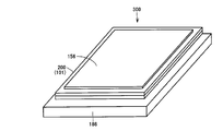
- FIG. 2 is a perspective view schematically showing a liquid crystal display device 300.
- FIG. 4 is a plan view schematically showing a liquid crystal display element 200.
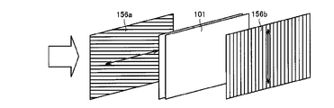
- FIG. 4 is an exploded perspective view showing an arrangement state of a liquid crystal display panel 101 and a polarizing plate 156.
- FIG. 2 is a plan view of a liquid crystal display panel 101.
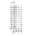
- FIG. 2 is a circuit diagram showing a thin film transistor array formed on an active matrix substrate 130.
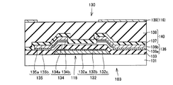
- FIG. 3 is a cross-sectional view of a liquid crystal display panel 101 in a display area 103.
- FIG. 2 is a cross-sectional view of an active matrix substrate 130 showing details of a thin film transistor 115.
- FIG. 10 It is a top view of the gate pad 112 formed in the peripheral circuit area.
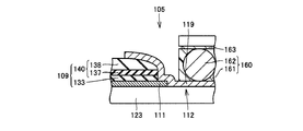
- FIG. 10 is a cross-sectional view taken along the line XX of FIG. 9 in a state where the anisotropic conductive film 160 and the gate driver 152 are disposed on the upper surface of the transparent conductive film 118A.
- FIG. 10 is a cross-sectional view taken along line XI-XI in FIG. 9.
- FIG. 10 is a cross-sectional view taken along line XII-XII in FIG. 9.
- FIG. 10 is a cross-sectional view taken along line XIII-XIII in FIG. 9. 3 is a cross-sectional view in a region that becomes a display region 103.
- FIG. 10 is a cross-sectional view taken along the line XX of FIG. 9 in a state where the anisotropic conductive film 160 and the gate driver 152 are disposed on the upper surface of the transparent conductive film 118A.
- FIG. 10 is a
- FIG. 15 is a cross-sectional view of a region to be a peripheral region 105 in the manufacturing process illustrated in FIG. 14.
- FIG. 16 is a cross-sectional view showing a manufacturing step after the manufacturing step shown in FIGS. 14 and 15.
- FIG. 17 is a cross-sectional view of a region to be a peripheral region 105 during the manufacturing process illustrated in FIG. 16. It is sectional drawing in the area
- FIG. 20 is a cross-sectional view of the display region 103 showing a manufacturing process after the manufacturing process shown in FIGS. 18 and 19.
- FIG. 21 is a cross-sectional view of a peripheral region 105 during the manufacturing process shown in FIG. 20.
- FIG. 6 is a cross-sectional view of a display region 103 in a liquid crystal display device according to a second embodiment. 4 is a plan view of a source pad 114 formed in a peripheral region 105.
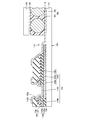
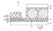
- FIG. FIG. 24 is a cross-sectional view taken along line XXIV-XXIV shown in FIG.
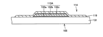
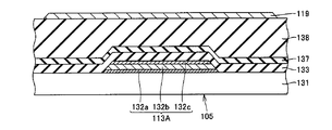
- FIG. 24 is a cross-sectional view taken along line XXV-XXV shown in FIG.
- FIG. 25 is a cross-sectional view taken along line XXVI-XXVI in FIG. 24.
- FIG. 25 is a cross-sectional view taken along line XXVII-XXVII in FIG. 24.
- FIG. 29 is a cross-sectional view showing a modified example of the source pad 114 shown in FIG. 28. It is sectional drawing of the liquid crystal display device which concerns on this Embodiment 4. 2 is a cross-sectional view of a gate pad 112. FIG. It is a top view of the liquid crystal display device as which COG (Chip On Glass) was employ
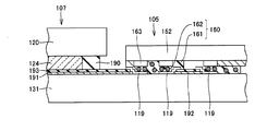
- FIG. 33 is a sectional view taken along line XXXIII-XXXIII shown in FIG. 32.
- a liquid crystal display device and a method for manufacturing the liquid crystal display device according to the present invention will be described with reference to FIGS.
- FIG. 1 is an exploded perspective view showing a configuration of a television receiver 500 according to Embodiment 1 of the present invention.
- a television receiver 500 includes a housing 181 disposed on the front surface side, a housing 182 disposed on the back surface, and a liquid crystal disposed between the housing 181 and the housing 182.
- a display device 300, an operation circuit 184, and a support member 185 are provided.
- the liquid crystal display device 300 is enclosed by the housing 181 and the housing 182, and is sandwiched between the housing 181 and the housing 182.
- An opening 183 is formed in the housing 181 so that an image displayed on the liquid crystal display device 300 can be transmitted to the outside.
- the housing 182 is provided with an operation circuit 184 for operating the liquid crystal display device 300.
- the housing 182 is supported by a support member 185.
- FIG. 2 is a perspective view schematically showing the liquid crystal display device 300.
- a liquid crystal display device 300 includes a liquid crystal display element 200 including a liquid crystal display panel 101, a polarizing plate 156 attached to one main surface of the liquid crystal display panel 101, and the other of the liquid crystal display panel 101. And a backlight unit 186 for irradiating the liquid crystal display panel 101 with light.
- FIG. 3 is a plan view schematically showing the liquid crystal display element 200.
- the liquid crystal display element 200 is connected to the liquid crystal display panel 101, the gate driver 152 connected to the gate terminal portion 150 of the liquid crystal display panel 101, and the source terminal portion 151 of the liquid crystal display panel 101.
- FIG. 4 is an exploded perspective view showing an arrangement state of the liquid crystal display panel 101 and the polarizing plate 156. As shown in FIG. 4, a polarizing plate 156a is mounted on one main surface of the liquid crystal display panel 101, and another polarizing plate 156b is mounted on the other main surface of the liquid crystal display panel 101.
- the polarizing axis direction of the polarizing plate 156a and the polarizing axis direction of the polarizing plate 156b are formed so as to be orthogonal to each other. Light from the backlight unit 186 shown in FIG. 2 is emitted to the polarizing plate 156a.
- the liquid crystal display panel 101 includes an active matrix substrate, a counter substrate disposed to be spaced from the active matrix substrate, and a liquid crystal layer sealed between the active matrix substrate and the counter substrate.
- a polarizing plate 156a is disposed on the side opposite to the liquid crystal layer with respect to the active matrix substrate, and a polarizing plate 156b is disposed on the side opposite to the liquid crystal layer with respect to the counter substrate.
- FIG. 5 is a plan view of the liquid crystal display panel 101.
- the liquid crystal display panel 101 includes a pixel array area 107 including a display area 103 and a non-display area 104, and a peripheral area 105 positioned around the pixel array area 107.
- the display area 103 is an area for displaying an image, and is formed by a plurality of pixels.
- the non-display area 104 is an area where no image is displayed, and is arranged around the display area 103.
- FIG. 6 is a circuit diagram showing a thin film transistor array formed on the active matrix substrate 130.
- the active matrix substrate 130 includes a pixel array region 107 and a transparent substrate 131 including a peripheral region 105 located around the pixel array region 107.
- a plurality of thin film transistors (switching elements) 115 are arranged on a portion of the main surface of the transparent substrate 131 where the display area 103 of the pixel arrangement area 107 is located.
- a plurality of gate lines (wirings) 111 connected to the gate electrode of the thin film transistor 115 and a plurality of data lines (wirings) 113 connected to the source electrode of the thin film transistor 115 are formed on the active matrix substrate 130.
- a pixel electrode 116 is connected to the drain electrode of the thin film transistor 115.
- the active matrix substrate 130 is usually rectangular.
- the gate lines 111 extend in the longitudinal direction of the active matrix substrate 130, and a plurality of gate lines 111 are formed at intervals in the short direction of the active matrix substrate 130.
- the data lines 113 extend in the short direction, and a plurality of data lines 113 are formed at intervals in the longitudinal direction.
- One pixel electrode 116 is disposed in a region surrounded by the gate line 111 and the data line 113.
- the gate line 111 is drawn from the thin film transistor 115 and extends from the pixel array region 107 to the peripheral region 105.
- a gate pad 112 is formed in a portion of the gate line 111 located on the peripheral region 105.
- the data line 113 is drawn from the thin film transistor 115 and extends from the pixel array region 107 to the peripheral region 105.
- a source pad 114 is formed in a portion of the data line 113 located on the peripheral region 105.
- FIG. 7 is a cross-sectional view of the liquid crystal display panel 101 in the display area 103.
- the counter substrate 120 includes a transparent substrate 123 such as a glass substrate, a color filter 121 formed on a main surface of the transparent substrate 123 that faces the active matrix substrate 130, and a color And a counter electrode 122 disposed on the active matrix substrate 130 side from the filter 121.
- the counter electrode 122 and the pixel electrode 116 are arranged so as to face each other with the liquid crystal layer 124 interposed therebetween.
- the active matrix substrate 130 includes a transparent substrate 131 such as a glass substrate and a thin film transistor 115 formed on the transparent substrate 131.
- FIG. 8 is a cross-sectional view of the active matrix substrate 130 showing details of the thin film transistor 115.
- the thin film transistor 115 includes a gate electrode 132 formed on the main surface of the transparent substrate 131 facing the counter substrate 120 and a gate insulation formed on the main surface of the transparent substrate 131 so as to cover the gate electrode 132.
- the semiconductor layer 134 is formed over the semiconductor layer 134 and the gate insulating film 133 so as to cover a part of the semiconductor layer 134 and the semiconductor layer 134 that is located over the gate electrode 132 and is located over the gate insulating film 133.
- a source electrode 135 and a drain electrode 136 that are spaced apart from each other.
- An interlayer insulating film 140 (passivation film and planarization film) is formed so as to cover the thin film transistor 115, and an ITO film 139 (pixel electrode 116) is formed on the interlayer insulating film 140.
- the pixel electrode 116 is electrically connected to the drain electrode 136.
- a contact hole (not shown) is formed in the interlayer insulating film 140, the pixel electrode 116 extends along the inner peripheral surface of the contact hole, and the pixel electrode 116 and the drain electrode 136 are connected. ing.
- the gate electrode 132 includes a metal film 132a formed on the main surface of the transparent substrate 131, a metal film 132b formed on the metal film 132a, and a metal film 132c formed on the metal film 132b.
- the metal film 132a and the metal film 132c are made of, for example, a metal material such as titanium (Ti), and the metal film 132b is made of a metal material such as aluminum (Al).
- a metal material such as titanium (Ti)
- Al aluminum
- the metal film 132a can be formed from molybdenum nitride (MoN)
- the metal film 132b can be formed from aluminum (Al)
- the metal film 132c can be formed from molybdenum (Mo).
- the gate insulating film 133 is made of, for example, silicon nitride (SiNx: x is a positive number) or the like.
- the semiconductor layer 134 is formed on the amorphous silicon film (a-Si film: i layer) 134a to be a channel portion of the thin film transistor 115 and the amorphous silicon film 134a, and an amorphous silicon film (n +) that is in contact with the source / drain electrodes. Layer) 134b.
- the source electrode 135 includes a metal film 135a formed of titanium or the like, and a metal film 135b formed on the metal film 135a and formed of aluminum or the like.
- the drain electrode 136 also includes a metal film 136a formed of titanium or the like and a metal film 136b formed on the metal film 136a and formed of aluminum or the like.
- the interlayer insulating film 140 includes a passivation film 137 and a planarization film 138 formed on the passivation film 137.
- the passivation film 137 is formed of a silicon nitride film, and is formed by, for example, a CVD (Chemical Vapor Deposition) method at about 250 degrees. Note that the passivation film 137 and the gate insulating film 133 are both formed of a silicon nitride film, but the gate insulating film 133 has a denser structure than the passivation film 137.
- the planarizing film 138 is formed from an organic material such as an acrylic-based synthetic resin. That is, the planarizing film 138 is an organic insulating film, and the passivation film 137 formed under the planarizing film 138 is an inorganic insulating film.
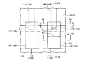
- FIG. 9 is a plan view of the gate pad 112 formed in the peripheral circuit region.
- the portion of the main surface of the transparent substrate 131 where the peripheral region 105 is located is exposed from insulating films such as the interlayer insulating film 140 and the gate insulating film 133. Note that the portion of the main surface of the transparent substrate 131 where the peripheral region 105 is located is exposed not only from the insulating film but also from the metal film constituting the semiconductor layer and the source and drain electrodes.
- the end portion 117A of the gate line 111A and the end portion 117B of the gate line 111B reach the peripheral region 105 and are exposed from the interlayer insulating film 140 and the gate insulating film 133.
- Transparent conductive films 118A and 118B are connected to the end portions 117A and 117B of the gate lines 111A and 111B.
- the transparent conductive films 118A and 118B are formed of, for example, an ITO film or an IZO (Indium Zinc Oxide) film.
- the transparent conductive films 118A and 118B are formed so as to cover the side surfaces and the upper surfaces of the end portions 117A and 117B from the main surface of the transparent substrate 131 exposed from the interlayer insulating film 140 and the gate insulating film 133. Thereby, electrical connection with transparent conductive film 118A, 118B and edge part 117A, 117B is securable. Gate pads 112A and 112B are formed by the transparent conductive films 118A and 118B.
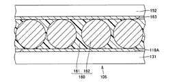
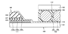
- FIG. 10 is a cross-sectional view taken along the line XX of FIG. 9, and shows a state in which the anisotropic conductive film 160 and the gate driver 152 are disposed on the upper surface of the transparent conductive film 118A.
- the portion of the transparent conductive film 118A located on the peripheral region 105 is a flat surface and functions as a terminal portion.
- An anisotropic conductive film 160 is disposed on the upper surface of the portion of the transparent conductive film 118A located on the main surface of the peripheral region 105, and the gate driver 152 is disposed on the upper surface of the anisotropic conductive film 160. Be placed.
- the anisotropic conductive film (connection member) 160 includes an insulating binder 161 and a plurality of conductive particles 162 disposed in the binder 161.
- a connection terminal (external terminal portion) 163 is disposed on the lower surface side of the gate driver 152.
- the conductive film 162 of the anisotropic conductive film 160 disposed between the transparent conductive film 118A and the connection terminal 163 of the gate driver 152 ensures electrical connection between the transparent conductive film 118A and the connection terminal 163. Has been.
- the conductive particles 162 are made of metal particles, and connect the transparent conductive film 118 ⁇ / b> A and the connection terminal 163.
- the transparent conductive film 118 and the anisotropic conductive film 160 are electrically connected at the contact portion (connection portion) between the transparent conductive film 118 and the anisotropic conductive film 160, and the anisotropic conductive film 160 Electrical connection between the anisotropic conductive film 160 and the connection terminal 163 is ensured at a contact portion (connection portion) with the connection terminal 163.
- the transparent conductive film 118A and the gate line 111A may be connected to each other, and even if the position of the end portion of the gate line 111A is displaced, the transparent conductive film 118A and the connection terminal 163 are not connected. Electrical connection can be ensured. For this reason, the yield of a liquid crystal display device can be improved.
- the main surface of the transparent substrate 131 located between the adjacent gate pads 112 ⁇ / b> A and 112 ⁇ / b> B is exposed from the interlayer insulating film 140 and the gate insulating film 133.
- the particle diameter of the conductive particles 162 can be kept small by bringing the connection terminal 163 and the transparent conductive films 118A and 118B close to each other.
- a plurality of conductive particles 162 are arranged on the transparent conductive film 118A, and a wide contact area between the conductive particles 162, the transparent conductive film 118A, and the connection terminals 163 is ensured. Can do.
- the small-diameter conductive particles 162 it is possible to suppress the single conductive particle 162 from being disposed so as to straddle between the gate pad 112A and the gate pad 112B.
- the occurrence of a short circuit with the gate pad 112B can be suppressed. Accordingly, even if the gate pad 112A and the gate pad 112B are brought close to each other, the occurrence of a short circuit between the gate pad 112A and the gate pad 112B can be suppressed, and the interval between the gate pad 112A and the gate pad 112B can be shortened. can do.
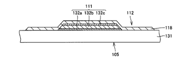
- FIG. 11 is a cross-sectional view taken along line XI-XI in FIG.
- the transparent conductive film 118 is formed over the peripheral surface and the upper surface of the end portion of the gate line 111. For this reason, electrical connection between the gate line 111 and the transparent conductive film 118 can be ensured.
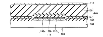
- FIG. 12 is a cross-sectional view taken along line XII-XII in FIG. 13 is a cross-sectional view taken along line XIII-XIII in FIG.
- the gate insulating film 133 and the interlayer insulating film are formed on the upper surface of the gate line 111 in a portion of the main surface of the transparent substrate 131 located on the display region 103 side with respect to the peripheral region 105. 140 is formed.
- the interlayer insulating film 140 includes a passivation film 137 formed on the gate insulating film 133 and a planarization film 138 formed on the passivation film 137.
- the transparent conductive film 118 is formed so as to reach the upper surface of the interlayer insulating film 140 from the main surface of the transparent substrate 131 located in the peripheral region 105 through the end of the gate line 111. .
- the end portion of the gate line 111 is located closer to the pixel array region 107 than the connection portion between the transparent conductive film 118 and the anisotropic conductive film 160.
- the anisotropic conductive film 160 and the transparent conductive film are included in the anisotropic conductive film 160.
- connection portion with 118 and a portion located in the vicinity thereof have a flat surface shape.
- the transparent conductive film 118 and the anisotropic conductive film 160 can be satisfactorily connected by making the connecting portion of the anisotropic conductive film 160 with the transparent conductive film 118 flat. .
- FIG. 14 is a cross-sectional view in a region that becomes the display region 103, and is a cross-sectional view when the gate electrode 132 is formed on the main surface of the transparent substrate 131.
- FIG. 15 is a cross-sectional view of a region to be the peripheral region 105 in the manufacturing process shown in FIG.
- a transparent substrate 131 having a main surface is prepared.
- the main surface of the transparent substrate 131 includes a region that becomes the display region 103 and a region that becomes the peripheral region 105.
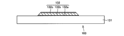
- a metal film 132 a, a metal film 132 b, and a metal film 132 c are formed on the main surface of the transparent substrate 131 in the region that becomes the peripheral region 105 and the region that becomes the display region 103.
- the gate electrode 132 and the gate line 111 are formed by patterning the laminated metal film.
- the gate electrode 132 and the gate line 111 are simultaneously formed by patterning the stacked metal films.
- FIG. 16 is a cross-sectional view showing a manufacturing process after the manufacturing process shown in FIGS. 14 and 15, and is a cross-sectional view in a region to be the display region 103.
- FIG. 17 is a cross-sectional view of a region that becomes the peripheral region 105 during the manufacturing process shown in FIG.
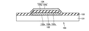
- an amorphous silicon film (i layer) 134a and an amorphous silicon film (n + layer) 134b formed on the amorphous silicon film 134a are sequentially stacked. Then, the laminated amorphous silicon film (i layer) 134a and amorphous silicon film (n + layer) 134b are patterned to form the semiconductor layer 134.
- the semiconductor layer 134 is formed on the upper surface of the gate insulating film 133 located above the gate electrode 132.
- the amorphous silicon film (i layer) 134a and the amorphous silicon film (n + layer) 134b are removed by the patterning.
- FIG. 18 is a cross-sectional view in a region that becomes a display region 103 showing a manufacturing process after the manufacturing process shown in FIGS. 16 and 17, and FIG. 19 is a peripheral region 105 in the manufacturing process shown in FIG. It is sectional drawing in an area
- a metal film formed of titanium or the like and a metal film formed of aluminum or the like are sequentially formed so as to cover the semiconductor layer 134.
- the laminated metal film is patterned. Thereby, the source electrode 135 and the drain electrode 136 are formed. Note that when the source electrode 135 and the drain electrode 136 are formed, the data line 113 is simultaneously formed. In this way, the thin film transistor 115 and the display region 103 are formed. A peripheral area 105 is defined around the display area 103.
- FIG. 20 is a cross-sectional view of the display area 103 showing the manufacturing process after the manufacturing process shown in FIGS. 18 and 19, and FIG. 21 is a cross-sectional view of the peripheral area 105 during the manufacturing process shown in FIG.
- a passivation film 137 and a planarization film 138 are formed so as to cover the source electrode 135, the drain electrode 136, the data line 113, and the like.
- the planarizing film 138 is formed from an organic material such as an acrylic-based synthetic resin. By patterning the planarizing film 138, a portion of the planarizing film 138 located in the peripheral region 105 is removed. In this patterning, for example, a contact hole or the like extending toward the drain electrode 136 is also formed in the planarizing film 138.
- the patterning is performed on the passivation film 137 and the gate insulating film 133 by using the planarized film 138 subjected to this patterning as a mask. Thereby, the passivation film 137 and the gate insulating film 133 formed on the peripheral region 105 are removed, and the main surface of the transparent substrate 131 is exposed to the outside. On the other hand, in the peripheral region 105, a contact hole that penetrates the planarizing film 138 and the passivation film 137 and reaches the drain electrode 136 is formed.
- an ITO film 139 is formed, and the ITO film 139 is patterned.
- the pixel electrode 116 is formed on the upper surface of the planarization film 138.
- the pixel electrode 116 is also formed in a contact hole that penetrates the planarization film 138 and the passivation film 137 and is electrically connected to the drain electrode 136.
- transparent conductive films 118A and 118B are formed.
- the width W2 of the transparent conductive film 118 is formed wider than the width W1 of the gate line 111. Therefore, when the ITO film 139 is patterned to form the transparent conductive film 118, even if a positional deviation or the like occurs in the mask, the connection between the transparent conductive film 118 and the gate line 111 can be secured. For this reason, the yield of the manufactured liquid crystal display device can be improved.
- the ITO film 139 when the ITO film 139 is patterned, a portion of the main surface of the transparent substrate 131 located in the peripheral region 105 is exposed from the interlayer insulating film 140 and the gate insulating film 133. For this reason, when the transparent conductive film 118 is formed by patterning the ITO film 139, it is sufficient that the transparent conductive film 118 and the gate line 111 are relatively aligned with each other. There is no need to consider. For this reason, since the number of objects that need to be accurately aligned is small, the yield of the liquid crystal display device can be improved.
- the relative positioning with respect to the gate line 111 only needs to be accurate, so that the margin in photolithography can be kept small.
- the gate pad 112 can be miniaturized.
- limiting in the shape of transparent conductive film 118 itself it is not restricted to the rectangular shape as shown in FIG. 9, Other polygonal shape, circular shape, elliptical shape, etc. can be employ
- the transparent conductive film 118 is formed so as to cover the end portion of the gate line 111 exposed from the interlayer insulating film 140 and the data line 113. Therefore, when the ITO film 139 is patterned to form the transparent conductive film 118 and the like, the gate line 111 can be prevented from being patterned, and the gate line 111 can be prevented from being disconnected. .
- the transparent conductive film 118 is formed so as to reach the upper surface of the interlayer insulating film 140, even if the transparent conductive film 118 is shifted from a predetermined position to the outer peripheral edge side of the transparent substrate 131, the transparent conductive film 118 is formed.
- the connection state between the film 118 and the gate line 111 can be maintained. Thereby, the yield of the liquid crystal display device to be manufactured can be improved.
- the ITO film 139 is patterned to form the transparent conductive film 118; however, the IZO film may be formed, and the IZO film may be patterned to form the transparent conductive film 118 and the like.
- a transparent conductive film other than the ITO film or the IZO film can also be employed.
- the metal film 132a is formed of molybdenum nitride (MoN)
- the metal film 132b is formed of aluminum (Al)
- the metal film 132c is formed of molybdenum (Mo)
- the gate insulating film 133 and the like are formed.
- Embodiment 2 A liquid crystal display device according to Embodiment 2 of the present invention will be described with reference to FIGS. Of the configurations shown in FIGS. 22 to 27, configurations that are the same as or similar to the configurations shown in FIGS. 1 to 21 are given the same reference numerals, and descriptions thereof are omitted.
- FIG. 22 is a cross-sectional view of the display region 103 in the liquid crystal display device according to the second embodiment.
- FIG. 23 is a plan view of the source pad 114 formed in the peripheral region 105.
- the end of the data line 113 reaches the portion of the main surface of the transparent substrate 131 where the peripheral region 105 is located.
- the end of the data line 113 reaching the peripheral region 105 is exposed from the gate insulating film 133 and the interlayer insulating film 140.
- a transparent conductive film 119 is connected to a portion of the data line 113 exposed from the gate insulating film 133 and the interlayer insulating film 140.
- the transparent conductive film 119 is formed so as to cover the end of the data line 113.
- the main surface of the transparent conductive film 119 and the transparent substrate 131 located around the transparent conductive film 119 is formed so as to be exposed from the interlayer insulating film 140 and the gate insulating film 133. Further, of the main surface of the transparent substrate 131, the main surface of the transparent substrate 131 located between the transparent conductive film 119A and the other transparent conductive film 119B adjacent to the transparent conductive film 119A is the gate insulating film 133 and the interlayer. The insulating film 140 is exposed.
- the transparent conductive film 119 is formed so as to reach the end of the data line 113 from the main surface of the transparent substrate 131. In the portion where the transparent substrate 131 is located on the end of the data line 113, the width W 4 of the transparent substrate 131 is formed wider than the width W 3 of the data line 113.
- the connection between the data line 113 and the transparent conductive film 119 can be secured even if the transparent conductive film 119 is slightly displaced in the width direction of the transparent conductive film 119. it can. Thereby, the yield of the liquid crystal display device can be improved.
- the transparent conductive film 119 is formed so as to reach the end of the data line 113 from the main surface of the transparent substrate 131.
- a portion of the transparent conductive film 119 located on the main surface of the transparent substrate 131 has a flat surface shape and functions as a terminal portion.
- a source pad 114 is formed by the transparent conductive film 119 thus formed.
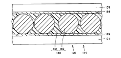
- FIG. 24 is a sectional view taken along line XXIV-XXIV shown in FIG.
- an anisotropic conductive film 160 is disposed on the upper surface of the transparent conductive film 119 located on the main surface of the transparent substrate 131.
- a source driver 153 is disposed on the upper surface of the anisotropic conductive film 160.
- a connection terminal 164 is formed on the lower surface of the source driver 153.
- the anisotropic conductive film 160 includes an insulating binder 161 and a plurality of conductive particles 162 provided in the binder 161.
- the transparent conductive film 119 and the connection terminal 164 are electrically connected by the conductive particles 162.
- connection terminal 164 and the source pad 114 can be brought close to each other.
- the connection terminal 164 and the transparent conductive film 119 can be brought close to each other, the small-diameter conductive particles 162 can be employed.
- a plurality of conductive particles 162 can be arrayed on the transparent conductive film 119, and a short circuit between the adjacent source pad 114A and the source pad 114B can be suppressed.
- FIG. 25 is a sectional view taken along line XXV-XXV shown in FIG.
- the data line 113 includes a data line main body 113B, a transparent conductive film 113C, and a connection wiring 113A.
- the data line main body 113B is connected to the source electrode 135 and is drawn from the source electrode 135 toward the peripheral region 105.
- the data line main body 113B includes a metal film 135a formed on the gate insulating film 133 and made of titanium or the like, and a metal film 135b formed on the metal film 135a and made of aluminum.
- connection wiring 113A is formed to extend from the end side of the data line main body 113B toward the peripheral region 105.
- the connection wiring 113A is formed of a metal film 132a, a metal film 132b, and a metal film 132c, and is formed of the same metal film as the gate line 111.
- the connection wiring 113 ⁇ / b> A is formed on the main surface of the transparent substrate 131.
- the connection wiring 113A is formed at the same time as the gate line 111 and the gate electrode 132 by laminating the metal film 132a, the metal film 132b, and the metal film 132c and then patterning them.
- An end portion of the connection wiring 113A reaches the peripheral region 105 and is formed so as to be exposed from the gate insulating film 133 and the interlayer insulating film 140.
- the transparent conductive film 113C is formed on the inner peripheral surface of the contact hole 165a formed so as to penetrate the planarizing film 138 and the passivation film 137.
- the end of the data line main body 113B is exposed in the contact hole 165a, and the upper surface of the connection wiring 113A is exposed at the bottom of the contact hole 165a.
- the transparent conductive film 113C passes through the upper surface of the connection wiring 113A, the peripheral surface and upper surface of the end portion of the data line main body 113B, and the inner peripheral surface of the contact hole 165a so as to reach the upper surface of the planarization film 138. Is formed. Therefore, the connection wiring 113A and the data line main body 113B are electrically connected by the transparent conductive film 113C.
- the planarizing film 138 is patterned.
- planarizing film 138 By patterning the planarizing film 138, a portion of the planarizing film 138 located in the peripheral region 105 is removed and a part of the contact hole 165a is formed.
- the contact hole 165a is formed by patterning the passivation film 137 using the patterned planarization film 138 as a mask. Furthermore, the main surface of the transparent substrate 131 in the peripheral region 105 is exposed outward.
- connection wiring 113A on the peripheral region 105 side is exposed from the planarization film 138, the passivation film 137, and the gate insulating film 133.
- the transparent conductive film 119 is formed so as to cover the end portion of the connection wiring 113 ⁇ / b> A and reach the upper surface of the planarization film 138. For this reason, even if the transparent conductive film 119 is displaced to the outer peripheral edge side of the transparent substrate 131, electrical connection between the transparent conductive film 119 and the connection wiring 113A can be ensured. For this reason, the yield of the manufactured liquid crystal display device can be improved.
- the transparent conductive film 119 is formed so as to cover a portion of the connection wiring 113A exposed from the insulating film such as the planarization film 138. Therefore, when the ITO film 139 is patterned to form the transparent conductive film 119, it is possible to prevent the connection wiring 113A from being patterned.
- 26 and 27 are cross-sectional views taken along lines XXVI-XXVI and XXVII-XXVII in FIG.
- the transparent conductive film 119 is formed from the main surface of the transparent substrate 131 adjacent to the connection wiring 113A to the upper surface and the peripheral surface of the connection wiring 113A.
- the transparent conductive film 119 is formed on the upper surface of the planarization film 138 on the display region 103 side with respect to the peripheral region 105.
- FIGS. 28 and 29 A liquid crystal display device according to the third embodiment will be described with reference to FIGS.
- FIGS. 28 and 29 configurations that are the same as or equivalent to the configurations shown in FIGS. 1 to 27 may be given the same reference numerals, and descriptions thereof may be omitted.
- FIG. 28 is a cross-sectional view of the peripheral region 105 in which the source pad 114 of the liquid crystal display device according to the third embodiment is formed.
- the data line 113 is formed so as to reach the peripheral region 105.
- the end of the data line 113 located in the peripheral area 105 is formed so as to reach the peripheral area 105.
- the end of the data line 113 is formed so as to be exposed from the interlayer insulating film 140.
- the interlayer insulating film 140 is formed so as to cover the display region 103 in which the thin film transistor 115 is formed.
- the data line 113 is formed on the gate insulating film 133 formed on the main surface of the transparent substrate 131.
- the gate insulating film 133 is also formed in the peripheral region 105.
- the transparent conductive film 118 is formed so as to reach the end of the data line 113 from the main surface of the transparent substrate 131 where the peripheral region 105 is located.
- the transparent conductive film 118 is formed so as to reach the upper surface of the interlayer insulating film 140 from the upper surface of the data line 113.
- the transparent conductive film 118 is formed on the upper surface of the gate insulating film 133 and is located above the main surface of the transparent substrate 131.
- An anisotropic conductive film (connecting member) 160 is disposed on the upper surface of the portion of the transparent conductive film 118 located on the main surface of the transparent substrate 131 where the peripheral region 105 is located.
- a portion of the transparent conductive film 118 positioned on the gate insulating film 133 is formed in a flat surface shape, and the connection terminal 163 of the gate driver 152 is disposed above the portion formed in the flat surface shape. Yes.
- An anisotropic conductive film 160 is disposed on the upper surface of the transparent conductive film 118, and the connection terminals 163 and the transparent conductive film 118 are electrically connected by the conductive particles 162 in the anisotropic conductive film 160. ing.
- the width of the transparent conductive film 118 is formed to be larger than the width of the end portion of the data line 113 as in the first and second embodiments.
- the end of the data line 113 does not need to be completely exposed from the interlayer insulating film 140.
- the end face of the data line 113 is exposed from the interlayer insulating film 140, and the transparent conductive film 118 is formed so as to be in contact with the end face of the data line 113.
- FIGS. 30 and 31 A liquid crystal display device according to the fourth embodiment will be described with reference to FIGS.
- the same or equivalent components as those shown in FIGS. 1 to 29 may be given the same reference numerals and explanation thereof may be omitted.
- FIG. 30 is a cross-sectional view of the liquid crystal display device according to the fourth embodiment, and FIG. 31 is a cross-sectional view of the gate pad 112.
- the gate electrode 132 and the gate line 111 are made of an aluminum alloy material film.
- the aluminum alloy material film includes aluminum as a base material, cobalt (Co), rhodium (Rh), nickel (Ni), palladium (Pd), carbon (C), silicon (Si), germanium (Ge), and An alloy component containing at least one element selected from the group consisting of tin (Sn), copper (Cu), lanthanum (La), boron (B), neodymium (Nd), silver (Ag), gold (Au ), Platinum (Pt), and other components containing at least one element selected from the group consisting of yttrium (Y).
- the gate line 111 and the gate electrode 132 can be patterned by wet etching.
- the gate electrode 132, the gate line 111, and the like are formed by patterning a laminated metal film of titanium and aluminum, dust such as titanium may be generated in the processing apparatus. When such dust is generated, the dust adheres to the substrate, which may lead to a decrease in yield.
- the gate line 111 and the gate electrode 132 it is possible to suppress the generation of dust by forming the gate line 111 and the gate electrode 132 by performing wet etching on the aluminum alloy material film as described above. Further, the potential difference between the aluminum alloy material film and the ITO film is smaller than the potential difference between the aluminum film and the ITO film. For this reason, even if the transparent conductive film 119 made of an ITO film or the like is brought into contact with the gate line 111, the gate line 111 can be prevented from being corroded.
- the insulating layer 109 includes a gate insulating film 133 and an interlayer insulating film 140 formed on the gate insulating film 133.
- the main surface of the transparent substrate 123 located in the peripheral region 105 is exposed from the insulating layer 109.
- the transparent conductive film 119 is formed so as to reach the end of the gate line 111 from the portion where the peripheral region 105 is located on the main surface of the transparent substrate 123.
- connection terminal 163 is above the flat surface portion. Has been placed.
- anisotropic conductive film 160 is arrange
- the metal films 135a and 136a of the source electrode 135 and the drain electrode 136 are made of molybdenum, and the metal films 135b and 136b are made of the aluminum alloy material film. ing.
- the source electrode 135 and the drain electrode 136 can be formed by wet etching.
- nickel or the like contained in the aluminum alloy material film can be prevented from diffusing into the semiconductor layer.
- 32 and 33 show an example in which the present invention is applied to COG (Chip On Glass).
- 32 is a plan view of a liquid crystal display device employing COG (Chip On Glass)
- FIG. 33 is a cross-sectional view taken along line XXXIII-XXXIII shown in FIG.
- a plurality of wirings 191 and wirings 192 are arranged on the main surface of the transparent substrate 131 where the peripheral region 105 is located.
- the wiring 191 is connected to the gate electrode, for example.
- the end of the wiring 191 is formed so as to be exposed from the insulating film 193 formed on the upper surface of the wiring 191.
- An end portion of the wiring 191 is located in the peripheral region 105, and a transparent conductive film 119 is connected to the end portion of the wiring 191.
- the transparent conductive film 119 is formed so as to reach the end of the wiring 191 from the main surface of the transparent substrate 131. And the part directly formed in the main surface of the transparent substrate 131 among the transparent conductive films 119 is made into flat surface shape. In the transparent conductive film 119, the connection terminal 163 of the gate driver 152 is disposed above the flat surface portion.
- An anisotropic conductive film 160 is disposed on the upper surface of the flat surface portion of the transparent conductive film 119, and the transparent conductive film 119 and the connection terminal 163 are electrically connected. Specifically, the connection terminal 163 and the transparent conductive film 119 are connected by the conductive particles 162 of the anisotropic conductive film 160.
- the present invention can be applied to a liquid crystal display device and a method of manufacturing the liquid crystal display device, and in particular, a liquid crystal display device having an active matrix substrate and a counter substrate and having terminal portions formed on the active matrix substrate It is suitable for the manufacturing method of the apparatus.
Landscapes
- Physics & Mathematics (AREA)
- Nonlinear Science (AREA)
- Mathematical Physics (AREA)
- Chemical & Material Sciences (AREA)
- Crystallography & Structural Chemistry (AREA)
- General Physics & Mathematics (AREA)
- Optics & Photonics (AREA)
- Geometry (AREA)
- Liquid Crystal (AREA)
- Devices For Indicating Variable Information By Combining Individual Elements (AREA)
Abstract
画素配列領域および周辺領域(105)を含む主表面を有する透明基板(131)と、画素配列領域に形成されたスイッチング素子と、透明基板(131)の主表面上に形成された層間絶縁膜(140)と、端部が層間絶縁膜(140)から露出するように形成された配線と、透明基板(131)の主表面から配線に達するように形成された透明導電膜(118)とを備え、透明基板(131)の主表面上に位置する透明導電膜(118)の上面上に異方性導電膜(160)が配置される。
Description
本発明は、液晶表示装置および液晶表示装置の製造方法に関し、特に、アクティブマトリックス基板および対向基板とを備え、アクティブマトリックス基板に形成された端子部を有する液晶表示装置および液晶表示装置の製造方法に関する発明である。
従来から各液晶表示装置が各種提案されている。液晶表示装置は、一般に、アクティブマトリックス基板と、アクティブマトリックス基板と対向するように配置された対向基板と、対向基板およびアクティブマトリックス基板間に配置された液晶層とを含む。
アクティブマトリックス基板には、ゲートパッドやソースパッドなどの端子部が複数設けられている。
たとえば、特開2000-199917号公報および特開平9-197433号公報に記載された液晶表示装置においては、層間絶縁膜に形成されたコンタクトホールから露出するソース端子やゲート端子が形成されている。
従来の液晶表示装置においては、層間絶縁膜にコンタクトホールを形成するときや、形成されたコンタクトホールにITO(Indium Tin Oxide)膜を所定の位置に形成するときなどにフォトリソグラフィによって、層間絶縁膜やITO膜をパターニングしている。
フォトリソグラフィを施す際には、位置ずれが生じたときのためにある程度のマージンを確保しておくのが一般的である。
その一方で、近年、端子部自体の幅および端子部間の間隔が狭くなっており、フォトリソグラフィを施す際のマージンを確保することが困難なものとなっている。
このため、従来の液晶表示装置および液晶表示装置の製造工程では、端子部のさらなる微細化を縮めることは困難なものとなっている。
本発明は、上記のような課題に鑑みてなされたものであって、その目的は、端子部の微細化が図られた液晶表示装置および液晶表示装置の製造方法を提供することである。
本発明に係る液晶表示装置は、画素配列領域および画素配列領域の周囲に形成された周辺領域を含む主表面を有する基板と、画素配列領域に形成されたスイッチング素子と、スイッチング素子に接続され、端部が周辺領域に達するように形成された配線と、周辺領域に位置する基板の主表面上から周辺領域に位置する配線の端部に達するように延びる透明導電膜と、透明導電膜の上方に配置された外部端子部と、透明導電膜のうち、基板の主表面上に形成された部分および外部端子部の間に配置され、透明導電膜と外部端子部とを電気的に接続する接続部材とを備える。
好ましくは、上記基板の主表面のうち、スイッチング素子が位置する領域を覆うように形成された絶縁膜をさらに備え、周辺領域に位置する配線の端部は、絶縁膜から露出するように形成される。上記透明導電膜および該透明導電膜の周囲に位置する基板の主表面は、絶縁膜から露出するように形成される。
好ましくは、上記配線の幅よりも、透明導電膜の幅の方が広くなるように形成される。
好ましくは、上記透明導電膜は、配線の上面および側面を覆うように形成される。
好ましくは、上記透明導電膜は、配線の上面および側面を覆うように形成される。
好ましくは、透明導電膜は、配線のうち、絶縁膜から露出する部分を覆うと共に、絶縁膜上に達するように形成される。好ましくは、配線の端部は、透明導電膜と接続部材との接続部分よりも、画素配列領域側に位置する。
本発明に係る液晶表示装置の製造方法は、画素配列領域となる第1領域、および画素配列領域の周囲に位置する周辺領域となる第2領域を含む主表面を有する基板を準備する工程と、第1領域にスイッチング素子を形成する工程と、スイッチング素子に接続され、第2領域に達するように形成された配線を形成する工程と、第2領域に位置する基板の主表面上から、配線の端部に達するように透明導電膜を形成する工程と、透明導電膜のうち、基板の主表面上に位置する部分の上面に接続部材を配置する工程と、接続部材の上面に外部端子を配置し、該外部端子および透明導電膜を電気的に接続する工程とを備える。
好ましくは、スイッチング素子を形成する工程は、第1領域にゲート電極を形成する工程と、ゲート電極上にゲート絶縁膜を形成する工程と、ゲート絶縁膜上に半導体層を形成する工程と、半導体層上にソース電極およびドレイン電極を形成する工程とを含む。上記配線は、ゲート電極またはソース電極に接続され、端部が第2領域に達するように形成される。上記ソース電極およびドレイン電極上に絶縁膜を形成する工程と、配線の端部を絶縁膜から露出させる工程とをさらに備え、透明導電膜は、絶縁膜から露出する配線の端部に接続されるように形成される。
好ましくは、透明導電膜の幅は、配線の端部の幅よりも幅広に形成される。好ましくは、透明導電膜は、絶縁膜から露出する配線の端部の上面および周面を覆うように形成される。好ましくは、上記透明導電膜は、絶縁膜上に達するように形成される。
本発明に係る液晶表示装置および液晶表示装置の製造方法によれば、端子部の微細化を図ることができる。
図1から図27を用いて、本発明に係る液晶表示装置および液晶表示装置の製造方法について説明する。
(実施の形態1)
図1は、本発明の実施の形態1に係るテレビジョン受信機500の構成を示す分解斜視図である。この図1に示すように、テレビジョン受信機500は、前面側に配置される筐体181と、背面側に配置される筐体182と、筐体181および筐体182間に配置された液晶表示装置300と、操作用回路184と、支持用部材185とを備えている。
図1は、本発明の実施の形態1に係るテレビジョン受信機500の構成を示す分解斜視図である。この図1に示すように、テレビジョン受信機500は、前面側に配置される筐体181と、背面側に配置される筐体182と、筐体181および筐体182間に配置された液晶表示装置300と、操作用回路184と、支持用部材185とを備えている。
液晶表示装置300は、筐体181および筐体182によって包み込まれ、筐体181および筐体182によって挟持されている。
筐体181には、開口部183が形成されており、液晶表示装置300に表示される画像を外部に透過可能とされている。筐体182には、液晶表示装置300を操作するための操作用回路184が設けられている。筐体182は、支持用部材185によって支持されている。
図2は、液晶表示装置300を模式的に示す斜視図である。この図2に示すように、液晶表示装置300は、液晶表示パネル101を含む液晶表示素子200と、液晶表示パネル101の一方の主表面に装着された偏光板156と、液晶表示パネル101の他方の主表面に装着された偏光板と、液晶表示パネル101に光を照射するバックライトユニット186とを備えている。
図3は、液晶表示素子200を模式的に示す平面図である。この図3に示すように、液晶表示素子200は、液晶表示パネル101と、液晶表示パネル101のゲート端子部150に接続されたゲートドライバ152と、液晶表示パネル101のソース端子部151に接続されたソースドライバ153と、ゲートドライバ152およびソースドライバ153が接続されたプリント基板配線154と、プリント基板配線154が接続された表示制御回路155とを備えている。
図4は、液晶表示パネル101および偏光板156との配置状態を示す分解斜視図である。この図4に示すように、液晶表示パネル101の一方の主表面には、偏光板156aが装着され、液晶表示パネル101の他方の主表面には、他の偏光板156bが装着されている。
なお、偏光板156aの偏光軸方向と、偏光板156bの偏光軸方向とは互いに直交するように形成されている。偏光板156aには、図2に示すバックライトユニット186からの光が放射される。
液晶表示パネル101は、アクティブマトリックス基板と、このアクティブマトリックス基板と対向するように、間隔をあけて配置された対向基板と、アクティブマトリックス基板および対向基板間に封入された液晶層とを含む。そして、アクティブマトリックス基板に対して液晶層と反対側に偏光板156aが配置され、対向基板に対して液晶層と反対側に偏光板156bが配置されている。
図5は、液晶表示パネル101の平面図である。この図5に示すように、液晶表示パネル101は、表示領域103および非表示領域104を含む画素配列領域107と、この画素配列領域107の周囲に位置する周辺領域105とを含む。
表示領域103は、画像を表示する領域であり、複数の画素により形成されている。非表示領域104は、画像を表示しない領域であり、表示領域103の周囲に配置されている。図6は、アクティブマトリックス基板130に形成された薄膜トランジスタアレイを示す回路図である。
アクティブマトリックス基板130は、画素配列領域107、および画素配列領域107の周囲に位置する周辺領域105を含む透明基板131を備える。
透明基板131の主表面のうち、画素配列領域107の表示領域103が位置する部分には、複数の薄膜トランジスタ(スイッチング素子)115が配列している。薄膜トランジスタ115のゲート電極に接続されるゲートライン(配線)111と、薄膜トランジスタ115のソース電極に接続されるデータライン(配線)113とが、アクティブマトリックス基板130に複数形成されている。薄膜トランジスタ115のドレイン電極には画素電極116が接続されている。
アクティブマトリックス基板130は、通常、長方形形状とされている。ゲートライン111は、アクティブマトリックス基板130の長手方向に延びており、ゲートライン111は、アクティブマトリックス基板130の短手方向に間隔をあけて複数形成されている。データライン113は、短手方向に延びており、長手方向に間隔をあけて複数形成されている。
ゲートライン111とデータライン113とによって囲まれる領域内に1つの画素電極116が配置されている。
ゲートライン111は、薄膜トランジスタ115から引き出され、画素配列領域107から周辺領域105に達するように延びている。そして、ゲートライン111のうち、周辺領域105上に位置する部分に、ゲートパッド112が形成されている。
データライン113は、薄膜トランジスタ115から引き出され、画素配列領域107から周辺領域105に達するように延びている。そして、データライン113のうち、周辺領域105上に位置する部分には、ソースパッド114が形成されている。
図7は、表示領域103における液晶表示パネル101の断面図である。図7に示すように、対向基板120は、ガラス基板などの透明基板123と、この透明基板123の主表面のうち、アクティブマトリックス基板130と対向する主表面に形成されたカラーフィルタ121と、カラーフィルタ121よりアクティブマトリックス基板130側に配置された対向電極122とを備えている。
そして、対向電極122と、画素電極116とは、液晶層124を挟んで互いに対向するように配置されている。アクティブマトリックス基板130は、ガラス基板などの透明基板131と、透明基板131上に形成された薄膜トランジスタ115とを備える。
図8は、薄膜トランジスタ115の詳細を示すアクティブマトリックス基板130の断面図である。薄膜トランジスタ115は、透明基板131の表面のうち、対向基板120と対向する主表面上に形成されたゲート電極132と、ゲート電極132を覆うように透明基板131の主表面上に形成されたゲート絶縁膜133と、ゲート絶縁膜133上に位置すると共に、ゲート電極132の上方に位置する半導体層134と、半導体層134の一部を覆うように半導体層134およびゲート絶縁膜133の上面上に形成され、互いに間隔をあけて形成されたソース電極135およびドレイン電極136とを備える。
そして、薄膜トランジスタ115を覆うように、層間絶縁膜140(パッシベーション膜および平坦化膜)が形成され、層間絶縁膜140上にITO膜139(画素電極116)が形成されている。この画素電極116は、ドレイン電極136と電気的に接続されている。具体的には、層間絶縁膜140に図示されていないコンタクトホールが形成されており、このコンタクトホールの内周面に沿って、画素電極116が延び、画素電極116とドレイン電極136とが接続されている。
ゲート電極132は、透明基板131の主表面上に形成された金属膜132aと、金属膜132a上に形成された金属膜132bと、この金属膜132b上に形成された金属膜132cとを含む。金属膜132aおよび金属膜132cは、たとえば、チタン(Ti)等の金属材料から形成されており、金属膜132bは、アルミニウム(Al)等の金属材料から形成されている。なお、各金属膜としては、上記の例に限られない。
たとえば、金属膜132aを窒化モリブデン(MoN)から形成し、金属膜132bをアルミニウム(Al)から形成し、さらに、金属膜132cをモリブデン(Mo)から形成することもできる。
ゲート絶縁膜133は、例えば、窒化シリコン(SiNx :xは正の数)等から形成されている。
半導体層134は、薄膜トランジスタ115のチャネル部となるアモルファスシリコン膜(a-Si膜:i層)134aと、アモルファスシリコン膜134a上に形成され、ソース・ドレイン電極とのコンタクトを図るアモルファスシリコン膜(n+層)134bとを含む。
ソース電極135は、チタン等から形成された金属膜135aと、この金属膜135a上に位置し、アルミニウム等から形成された金属膜135bとを含む。ドレイン電極136も、チタン等から形成された金属膜136aと、この金属膜136a上に形成され、アルミニウム等から形成された金属膜136bとを含む。
層間絶縁膜140は、パッシベーション膜137と、パッシベーション膜137上に形成された平坦化膜138とを含む。パッシベーション膜137は、窒化シリコン膜から形成されており、たとえば、250度程度でCVD(Chemical Vapor Deposition)法により形成する。なお、パッシベーション膜137と、ゲート絶縁膜133とは、いずれも窒化シリコン膜により形成されているが、ゲート絶縁膜133の方がパッシベーション膜137よりも組織が緻密である。
平坦化膜138は、アクリルベースの合成樹脂等の有機材料から形成されている。すなわち、平坦化膜138は、有機絶縁膜であり、平坦化膜138下に形成されたパッシベーション膜137は無機絶縁膜である。
図9は、周辺回路領域に形成されたゲートパッド112の平面図である。この図9に示すように、透明基板131の主表面のうち、周辺領域105が位置する部分は、層間絶縁膜140およびゲート絶縁膜133等の絶縁膜から露出している。なお、透明基板131の主表面のうち、周辺領域105が位置する部分は、絶縁膜のみならず、半導体層やソース電極およびドレイン電極を構成する金属膜からも露出している。
そして、ゲートライン111Aの端部117Aおよびゲートライン111Bの端部117Bは、周辺領域105に達すると共に、層間絶縁膜140およびゲート絶縁膜133から露出するように形成されている。
ゲートライン111A,111Bの端部117A,117Bには、透明導電膜118A,118Bが接続されている。透明導電膜118A,118Bは、たとえば、ITO膜またはIZO(Indium Zinc Oxide)膜等から形成されている。
この透明導電膜118A,118Bは、層間絶縁膜140およびゲート絶縁膜133から露出する透明基板131の主表面から端部117A,117Bの側面および上面を覆うように形成されている。これにより、透明導電膜118A,118Bおよび端部117A,117Bとの電気的な接続を確保することができる。この透明導電膜118A,118Bによって、ゲートパッド112A,112Bが形成されている。
図10は、図9のX-X線における断面であって、この透明導電膜118Aの上面に異方性導電膜160およびゲートドライバ152を配置した状態における断面図である。
この図10および上記図9に示すように、透明導電膜118Aのうち、周辺領域105上に位置する部分は、平坦面とされており、端子部として機能する。
そして、透明導電膜118Aのうち、周辺領域105の主表面上に位置する部分の上面には、異方性導電膜160が配置され、この異方性導電膜160の上面上にゲートドライバ152が配置される。
異方性導電膜(接続部材)160は、絶縁性のバインダ161と、このバインダ161内に複数配置された導電性の導電性粒子162とを含む。ゲートドライバ152の下面側には、接続端子(外部端子部)163が配置されている。そして、透明導電膜118Aとゲートドライバ152の接続端子163との間に配置された異方性導電膜160の導電性粒子162によって、透明導電膜118Aと接続端子163との電気的な接続が確保されている。
導電性粒子162は、金属製の粒子によって構成されており、透明導電膜118Aと接続端子163とを接続している。このように、透明導電膜118と異方性導電膜160との接触部分(接続部分)で透明導電膜118と異方性導電膜160とが電気的に接続され、異方性導電膜160と接続端子163との接触部分(接続部分)で異方性導電膜160と接続端子163との電気的な接続が確保されている。ここで、透明導電膜118Aとゲートライン111Aとは、互いに接続されておればよく、ゲートライン111Aの端部の位置が、仮に、位置ずれしたとしても、透明導電膜118Aと接続端子163との電気的な接続を確保することができる。このため、液晶表示装置の歩留まりの向上を図ることができる。上記図9に示すように、隣り合うゲートパッド112A,112B間に位置する透明基板131の主表面は層間絶縁膜140およびゲート絶縁膜133から露出している。
このため、接続端子163と透明導電膜118A,118Bとを互いに近接させることで、導電性粒子162の粒径を小さく抑えることができる。小径の導電性粒子162を採用することで、複数の導電性粒子162が透明導電膜118A上に配列し、導電性粒子162と透明導電膜118Aおよび接続端子163との接触面積を広く確保することができる。
さらに、小径の導電性粒子162を採用することで、1つの導電性粒子162がゲートパッド112Aとゲートパッド112Bとの間を跨るように配置されることを抑制することができ、ゲートパッド112Aとゲートパッド112Bとの間で短絡が発生することを抑制することができる。これに伴い、ゲートパッド112Aとゲートパッド112Bとを近接させたとしても、ゲートパッド112Aおよびゲートパッド112B間における短絡の発生を抑制することができ、ゲートパッド112Aおよびゲートパッド112B間の間隔を短くすることができる。
図11は、上記図9のXI-XI線における断面図である。この図11に示すように、透明導電膜118は、ゲートライン111の端部の周面および上面上に亘って形成されている。このため、ゲートライン111と、透明導電膜118との電気的接続を確保することができる。
図12は、図9のXII-XII線における断面図である。図13は、図9のXIII-XIII線における断面図である。この図12および図13に示すように、透明基板131の主表面のうち、周辺領域105よりも表示領域103側に位置する部分では、ゲートライン111の上面上にゲート絶縁膜133および層間絶縁膜140が形成されている。なお、層間絶縁膜140は、ゲート絶縁膜133上に形成されたパッシベーション膜137およびパッシベーション膜137上に形成された平坦化膜138を含む。
図13に示すように、透明導電膜118は、周辺領域105に位置する透明基板131の主表面からゲートライン111の端部上をとおり、層間絶縁膜140の上面に達するように形成されている。図13および上記図9に示すように、ゲートライン111の端部は、透明導電膜118と異方性導電膜160との接続部分よりも、画素配列領域107側に位置している。このように、ゲートライン111が、異方性導電膜160と透明導電膜118との接触部分から退避しているので、異方性導電膜160のうち、異方性導電膜160と透明導電膜118との接続部分およびその近傍に位置する部分が平坦面状となる。このように、異方性導電膜160のうち、透明導電膜118との接続部分を平坦面状とすることで、透明導電膜118と異方性導電膜160とを良好に接続することができる。
上記のように構成された液晶表示装置の製造方法について説明する。
図14は、表示領域103となる領域における断面図であり、透明基板131の主表面上にゲート電極132を形成したときの断面図である。図15は、上記図14に示す製造工程において、周辺領域105となる領域における断面図である。
図14は、表示領域103となる領域における断面図であり、透明基板131の主表面上にゲート電極132を形成したときの断面図である。図15は、上記図14に示す製造工程において、周辺領域105となる領域における断面図である。
この図14および図15に示すように、まず、主表面を有する透明基板131を準備する。なお、透明基板131の主表面は、表示領域103となる領域と、周辺領域105となる領域とを含む。そして、透明基板131の主表面のうち、周辺領域105となる領域および表示領域103となる領域に金属膜132a、金属膜132bおよび金属膜132cを形成する。そして、この積層された金属膜をパターニングすることでゲート電極132およびゲートライン111を形成する。ゲート電極132と、ゲートライン111とは、積層された金属膜をパターニングすることで同時に形成される。
図16は、上記図14および図15に示す製造工程後の製造工程を示す断面図であり、表示領域103となる領域における断面図である。図17は、図16に示す製造工程時において、周辺領域105となる領域における断面図である。
この図16および図17に示すように、アモルファスシリコン膜(i層)134aと、アモルファスシリコン膜134a上に形成されたアモルファスシリコン膜(n+層)134bとを順次積層する。そして、積層されたアモルファスシリコン膜(i層)134aとアモルファスシリコン膜(n+層)134bとをパターニングして、半導体層134を形成する。半導体層134は、ゲート電極132の上方に位置するゲート絶縁膜133の上面上に形成されている。
なお、周辺領域105となる領域においては、アモルファスシリコン膜(i層)134aと、アモルファスシリコン膜(n+層)134bとは、上記パターニングによって除去される。
図18は、上記図16および図17に示す製造工程後の製造工程を示す表示領域103となる領域における断面図であり、図19は、上記図18に示す製造工程時における周辺領域105となる領域における断面図である。
半導体層134を覆うように、チタン等から形成された金属膜およびアルミニウムなどから形成された金属膜を順次成膜する。
そして、上記積層された金属膜をパターニングする。これにより、ソース電極135およびドレイン電極136が形成される。なお、ソース電極135およびドレイン電極136が形成される際に、同時にデータライン113が形成される。このようにして、薄膜トランジスタ115および表示領域103が形成される。そして、表示領域103の周囲に周辺領域105が規定される。
図20は、図18および図19に示す製造工程後の製造工程を示す表示領域103の断面図であり、図21は、図20に示す製造工程時における周辺領域105の断面図である。この図20および図21に示すように、ソース電極135、ドレイン電極136およびデータライン113等を覆うようにパッシベーション膜137および平坦化膜138が形成される。
平坦化膜138は、アクリルベースの合成樹脂等の有機材料から形成されている。この平坦化膜138をパターニングすることで、平坦化膜138のうち周辺領域105に位置する部分が除去される。なお、このパターニングの際に、たとえば、ドレイン電極136に向けて延びるコンタクトホール等も、平坦化膜138に形成される。
このパターニングが施された平坦化膜138をマスクとして、パッシベーション膜137およびゲート絶縁膜133にパターニングが施される。これにより、周辺領域105上に形成されたパッシベーション膜137およびゲート絶縁膜133が除去され、透明基板131の主表面が外方に露出する。その一方で周辺領域105内においては、平坦化膜138およびパッシベーション膜137を貫通し、ドレイン電極136に達するコンタクトホールが形成される。
その後、図8に示すように、ITO膜139を形成し、このITO膜139をパターニングする。これにより、平坦化膜138の上面上には、画素電極116が形成される。この画素電極116は、平坦化膜138およびパッシベーション膜137を貫通するコンタクトホールにも形成され、ドレイン電極136に電気的に接続される。
その一方で、周辺領域105においては、図9に示すように、透明導電膜118A,118Bが形成される。
ここで、透明導電膜118の幅W2は、ゲートライン111の幅W1よりも幅広に形成されている。このため、ITO膜139をパターニングして、透明導電膜118を形成する際に、マスクに位置ずれ等が生じたとしても、透明導電膜118とゲートライン111との接続を確保することができる。このため、製造される液晶表示装置の歩留まりの向上を図ることができる。
さらに、ITO膜139をパターニングする際において、透明基板131の主表面のうち、周辺領域105に位置する部分は、層間絶縁膜140およびゲート絶縁膜133から露出している。このため、ITO膜139をパターニングして透明導電膜118を形成する際には、透明導電膜118とゲートライン111との相対的な位置あわせがなされておればよく、他の部材との位置あわせを考慮する必要がない。このため、位置あわせを正確に行う必要のある対象が少ないため液晶表示装置の歩留まりの向上を図ることができる。
透明導電膜118を形成する際には、ゲートライン111との相対的な位置決めが正確であればよいため、フォトリソグラフィにおけるマージンを小さく抑えることができる。
このように、フォトリソグラフィにおけるマージンを小さく抑えることができるので、透明導電膜118同士間の間隔を小さくしたり、透明導電膜118の幅W2自体を小さくすることができる。このため、ゲートパッド112の微細化を図ることができる。また、透明導電膜118自体の形状に制約がないため、図9に示すような長方形形状に限られず、他の多角形形状、円形形状、および楕円形状等を採用することができる。
透明導電膜118は、層間絶縁膜140およびデータライン113から露出するゲートライン111の端部を覆うように形成されている。このため、ITO膜139をパターニングして透明導電膜118等を形成する際に、ゲートライン111までもパターニングされることを抑制することができ、ゲートライン111が断線することを抑制することができる。
また、透明導電膜118は、層間絶縁膜140の上面に達するように形成されているので、透明導電膜118が、所定の位置から透明基板131の外周縁部側にずれたとしても、透明導電膜118とゲートライン111との接続状態を維持することができる。これにより、製造する液晶表示装置の歩留まりの向上を図ることができる。なお、ITO膜139をパターニングして、透明導電膜118を形成しているが、IZO膜を形成し、このIZO膜をパターニングすることで透明導電膜118等を形成するようにしてもよい。さらに、ITO膜やIZO膜以外の透明導電膜をも採用することができる。また、金属膜132aを窒化モリブデン(MoN)から形成し、金属膜132bをアルミニウム(Al)から形成し、さらに、金属膜132cをモリブデン(Mo)から形成した場合においても、ゲート絶縁膜133等をパターニングする際に、耐薬性を確保することができる。
(実施の形態2)
図22から図27を用いて、本発明の実施の形態2に係る液晶表示装置について説明する。なお、図22から図27に示す構成のうち、上記図1から図21に示す構成と同一または相等する構成については、同一の符号を付してその説明を省略する。
図22から図27を用いて、本発明の実施の形態2に係る液晶表示装置について説明する。なお、図22から図27に示す構成のうち、上記図1から図21に示す構成と同一または相等する構成については、同一の符号を付してその説明を省略する。
図22は、本実施の形態2に係る液晶表示装置における表示領域103における断面図である。図23は、周辺領域105に形成されたソースパッド114の平面図である。
この図23に示すように、データライン113の端部は、透明基板131の主表面のうち、周辺領域105が位置する部分に達している。データライン113のうち、周辺領域105に達する端部は、ゲート絶縁膜133および層間絶縁膜140から露出している。データライン113のうち、ゲート絶縁膜133および層間絶縁膜140から露出する部分には、透明導電膜119が接続されている。透明導電膜119は、データライン113の端部を覆うように形成されている。
透明導電膜119およびその周囲に位置する透明基板131の主表面は、層間絶縁膜140およびゲート絶縁膜133から露出するように形成されている。さらに、透明基板131の主表面のうち、透明導電膜119Aと、透明導電膜119Aと隣り合う他の透明導電膜119Bとの間の位置する透明基板131の主表面は、ゲート絶縁膜133および層間絶縁膜140から露出している。
透明導電膜119は、透明基板131の主表面上からデータライン113の端部に達するように形成されている。透明基板131がデータライン113の端部上に位置する部分において、透明基板131の幅W4は、データライン113の幅W3よりも幅広に形成されている。
このため、透明導電膜119を成膜する際に、透明導電膜119が透明導電膜119の幅方向に多少位置ずれしたとしても、データライン113と透明導電膜119との接続を確保することができる。これにより、液晶表示装置の歩留まりの向上を図ることができる。
透明導電膜119は、透明基板131の主表面からデータライン113の端部に達するように形成されている。透明導電膜119のうち、透明基板131の主表面上に位置する部分は、平坦面状とされており、端子部として機能する。このように形成された透明導電膜119によって、ソースパッド114が形成されている。
図24は、図23に示すXXIV-XXIV線における断面図である。この図24に示すように、透明基板131の主表面上に位置する透明導電膜119の上面上には、異方性導電膜160が配置されている。この異方性導電膜160の上面上には、ソースドライバ153が配置されている。ソースドライバ153の下面には、接続端子164が形成されている。
異方性導電膜160は、絶縁性のバインダ161と、バインダ161内に複数設けられてた導電性粒子162とを含む。そして、導電性粒子162によって、透明導電膜119と接続端子164とが電気的に接続されている。
ソースパッド114においても、ソースパッド114の周囲には、層間絶縁膜140およびゲート絶縁膜133が形成されていないため、接続端子164とソースパッド114(透明導電膜119)とを近接させることができる。接続端子164と透明導電膜119とを近接させることができるので、小径の導電性粒子162を採用することができる。
これに伴い、透明導電膜119上に複数の導電性粒子162を配列させることができると共に、隣り合うソースパッド114Aとソースパッド114Bとが短絡することを抑制することができる。
図25は、図23に示すXXV-XXV線における断面図である。この図25に示すように、データライン113は、データライン本体部113Bと、透明導電膜113Cと、接続配線113Aとを備えている。
データライン本体部113Bは、ソース電極135に接続され、ソース電極135から周辺領域105に向けて引き出されている。このデータライン本体部113Bは、ゲート絶縁膜133上に形成され、チタン等から形成された金属膜135aと、この金属膜135a上に形成され、アルミニウムから形成された金属膜135bとを含む。
接続配線113Aは、データライン本体部113Bの端部側から周辺領域105に向けて延びるように形成されている。この接続配線113Aは、金属膜132aと、金属膜132bと、金属膜132cとによって形成されており、ゲートライン111と同様の金属膜により形成されている。接続配線113Aは、透明基板131の主表面上に形成されている。この接続配線113Aは、金属膜132aと、金属膜132bと、金属膜132cとを積層した後、パターニングすることでゲートライン111およびゲート電極132と同時に形成される。この接続配線113Aの端部が周辺領域105に達しており、ゲート絶縁膜133および層間絶縁膜140から露出するように形成されている。
透明導電膜113Cは、平坦化膜138およびパッシベーション膜137を貫通するように形成されたコンタクトホール165aの内周面上に形成されている。コンタクトホール165a内には、データライン本体部113Bの端部が露出しており、コンタクトホール165aの底部には、接続配線113Aの上面が露出している。
そして、透明導電膜113Cは、接続配線113Aの上面、データライン本体部113Bの端部の周面および上面、およびコンタクトホール165aの内周面を通って、平坦化膜138の上面に達するように形成されている。このため、接続配線113Aとデータライン本体部113Bとは、透明導電膜113Cによって電気的に接続されている。
なお、コンタクトホール165aを形成する際には、まず、パッシベーション膜137および平坦化膜138を形成した後、平坦化膜138をパターニングする。
平坦化膜138をパターニングすることで、平坦化膜138のうち、周辺領域105に位置する部分が除去されると共に、コンタクトホール165aの一部が形成される。
そして、このパターニングされた平坦化膜138をマスクとして、パッシベーション膜137をパターニングすることで、コンタクトホール165aが形成される。さらに、周辺領域105における透明基板131の主表面が外方に露出する。
接続配線113Aの周辺領域105側の端部は、平坦化膜138、パッシベーション膜137およびゲート絶縁膜133から露出してる。そして、透明導電膜119は、接続配線113Aの端部を覆うと共に、平坦化膜138の上面に達するように形成されている。このため、透明導電膜119が透明基板131の外周縁部側に位置ずれしたとしても、透明導電膜119と接続配線113Aとの電気的な接続を確保することがでできる。このため、製造される液晶表示装置の歩留まりの向上を図ることができる。
さらに、透明導電膜119は、接続配線113Aのうち、平坦化膜138等の絶縁膜から露出する部分を覆うように形成されている。このため、ITO膜139をパターニングして透明導電膜119を形成する際に、接続配線113Aまでもパターニングされることを抑制することができる。
なお、図26および図27は、図24におけるXXVI-XXVI線およびXXVII-XXVII線における断面図である。
図26に示すように、透明導電膜119は、接続配線113Aと隣り合う透明基板131の主表面から接続配線113Aの上面および周面上に亘って形成されている。そして、周辺領域105よりも表示領域103側では、透明導電膜119は、平坦化膜138の上面上に形成されている。
(実施の形態3)
図28および図29を用いて、本実施の形態3に係る液晶表示装置について説明する。なお、図28および図29に示す構成のうち、上記図1から図27に示す構成と同一または相当する構成については、同一の符号を付して説明を省略する場合がある。
図28および図29を用いて、本実施の形態3に係る液晶表示装置について説明する。なお、図28および図29に示す構成のうち、上記図1から図27に示す構成と同一または相当する構成については、同一の符号を付して説明を省略する場合がある。
図28は、本実施の形態3に係る液晶表示装置のソースパッド114が形成された周辺領域105の断面図である。
この図28に示すように、データライン113は、周辺領域105に達するように形成されている。周辺領域105に位置するデータライン113の端部は、周辺領域105に達するように形成されている。このデータライン113の端部は、層間絶縁膜140から露出するように形成されている。なお、層間絶縁膜140は、薄膜トランジスタ115が形成された表示領域103を覆うように形成されている。
データライン113は、透明基板131の主表面上に形成されたゲート絶縁膜133上に形成されている。本実施の形態に係る液晶表示装置においては、ゲート絶縁膜133は、周辺領域105にも形成されている。
透明導電膜118は、周辺領域105が位置する透明基板131の主表面上からデータライン113の端部に達するように形成されている。そして、透明導電膜118は、データライン113の上面から層間絶縁膜140の上面に達するように形成されている。
透明導電膜118は、上記ゲート絶縁膜133の上面上に形成されており、透明基板131の主表面の上方に位置している。透明導電膜118のうち、周辺領域105が位置する透明基板131の主表面上に位置する部分の上面には、異方性導電膜(接続部材)160が配置されている。
透明導電膜118のうち、ゲート絶縁膜133上に位置する部分は、平坦面状に形成されており、この平坦面状に形成された部分の上方にゲートドライバ152の接続端子163が配置されている。透明導電膜118の上面上に異方性導電膜160が配置されており、この異方性導電膜160内の導電性粒子162によって、接続端子163と透明導電膜118とが電気的に接続されている。
このため、データライン113の端部の位置が位置ずれした場合においても、データライン113の端部と透明導電膜118とが接続されておればよく、歩留まりの向上を図ることができる。さらに、このソースパッド114においても、上記実施の形態1および実施の形態2と同様に、透明導電膜118の幅は、データライン113の端部の幅よりも大きくなるように形成されている。
なお、データライン113の端部は、層間絶縁膜140から完全に露出してい必要はない。たとえば、図29に示す例においては、データライン113の端面が層間絶縁膜140から露出しており、透明導電膜118がデータライン113の端面と接触するように、形成されている。
(実施の形態4)
図30および図31を用いて、本実施の形態4に係る液晶表示装置について説明する。なお、図30および図31に示す構成のうち、上記図1から図29に示す構成と同一または相当する構成については、同一の符号を付してその説明を省略する場合がある。
図30および図31を用いて、本実施の形態4に係る液晶表示装置について説明する。なお、図30および図31に示す構成のうち、上記図1から図29に示す構成と同一または相当する構成については、同一の符号を付してその説明を省略する場合がある。
図30は、本実施の形態4に係る液晶表示装置の断面図であり、図31は、ゲートパッド112の断面図である。
図30において、ゲート電極132およびゲートライン111は、アルミニウム合金材料膜によって構成されている。
このアルミニウム合金材料膜は、母材としてのアルミニウムと、コバルト(Co),ロジウム(Rh),ニッケル(Ni),パラジウム(Pd),炭素(C),ケイ素(Si),ゲルマニウム(Ge)、およびスズ(Sn)よりなる群から選択される少なくとも1種の元素を含む合金成分と、銅(Cu)、ランタン(La)、ホウ素(B)、ネオジム(Nd)、銀(Ag)、金(Au)、白金(Pt)、およびイットリウム(Y)よりなる群から選択される少なくとも1種の元素を含む他の成分とを有する。
このようなアルミニウム合金材料膜でゲートライン111およびゲート電極132を構成することで、ウエットエッチングでゲートライン111およびゲート電極132をパターニングすることができる。
たとえば、チタンおよびアルミニウムの積層金属膜をパターニングして、ゲート電極132およびゲートライン111等を形成する場合には、処理装置内にチタンなどのダストが発生するおそれがある。このようなダストが発生すると、ダストが基板上に付着し、歩留まりの低下を招くおそれがある。
その一方で、上記のようなアルミニウム合金材料膜をウエットエッチングすることで、ゲートライン111およびゲート電極132を形成することで、上記ダストが発生することを抑制することができる。さらに、上記アルミニウム合金材料膜とITO膜との電位差は、アルミニウム膜とITO膜との電位差よりも小さい。このため、ゲートライン111にITO膜等から構成された透明導電膜119を接触したとしても、ゲートライン111が腐食されることを抑制することができる。
ここで、図31に示すように、ゲートライン111の端部は、絶縁層109から露出している。なお、絶縁層109は、ゲート絶縁膜133と、このゲート絶縁膜133上に形成された層間絶縁膜140とを含む。
なお、本実施の形態4においても、周辺領域105に位置する透明基板123の主表面は、絶縁層109から露出している。
そして、透明導電膜119は、透明基板123の主表面のうち、周辺領域105が位置する部分からゲートライン111の端部に達するように形成されている。
そして、透明導電膜119のうち、透明基板123の主表面上に直接形成された部分は、平坦面状に形成されている、この平坦面状とされた部分の上方には、接続端子163が配置されている。
そして、透明導電膜119のうち、平坦面状とされた部分の上面には、異方性導電膜160が配置されており、透明導電膜119と接続端子163とが電気的に接続されている。
本実施の形態4に係る液晶表示装置においては、ソース電極135およびドレイン電極136の金属膜135a,136aは、モリブデンから形成されており、金属膜135b,136bは、上記アルミニウム合金材料膜から構成されている。
このように、ソース電極135およびドレイン電極136を形成することで、ソース電極135およびドレイン電極136をウエットエッチングにより形成することができる。
さらに、アルミニウム合金材料膜の下面にモリブデンから構成された金属膜を配置することで、アルミニウム合金材料膜に含まれるニッケル等が半導体層に拡散することを抑制することができる。
なお、図32および図33は、本発明をCOG(Chip On Glass)に適用した例を示す。
図32は、COG(Chip On Glass)が採用された液晶表示装置の平面図であり、図33は、図32に示すXXXIII-XXXIII線の断面図である。
図32は、COG(Chip On Glass)が採用された液晶表示装置の平面図であり、図33は、図32に示すXXXIII-XXXIII線の断面図である。
この図32に示すように、透明基板131の主表面のうち、周辺領域105が位置する分には、複数の配線191および配線192が配置されている。配線191は、たとえば、ゲート電極に接続されている。
この配線191の端部は、配線191の上面に形成された絶縁膜193から露出するように形成されている。配線191の端部は、周辺領域105に位置しており、この配線191の端部には、透明導電膜119が接続されている。
ここで、透明導電膜119は、透明基板131の主表面から配線191の端部に達するように形成されている。そして、透明導電膜119のうち、透明基板131の主表面に直接形成された部分は、平坦面状とされている。透明導電膜119のうち、上記平坦面部分の上方にゲートドライバ152の接続端子163が配置されている。
透明導電膜119の平坦面部分の上面に異方性導電膜160が配置され、透明導電膜119と接続端子163とが電気的に接続されている。具体的には、異方性導電膜160の導電性粒子162によって、接続端子163と透明導電膜119とが接続されている。
以上のように本発明の実施の形態について説明を行なったが、今回開示された実施の形態はすべての点で例示であって制限的なものではないと考えられるべきである。本発明の範囲は請求の範囲によって示され、請求の範囲と均等の意味および範囲内での0および範囲にかぎられない。
本発明は、液晶表示装置および液晶表示装置の製造方法に適用することができ、特に、アクティブマトリックス基板および対向基板とを備え、アクティブマトリックス基板に形成された端子部を有する液晶表示装置および液晶表示装置の製造方法に好適である。
101 液晶表示パネル、103 表示領域、104 非表示領域、105 周辺領域、107 画素配列領域、111 ゲートライン、112 ゲートパッド、113 データライン、113A 接続配線、113B データライン本体部、113C 透明導電膜、114 ソースパッド、115 薄膜トランジスタ、116 画素電極、118 透明導電膜、119 透明導電膜、120 対向基板、121 カラーフィルタ、122 対向電極、123 透明基板、124 液晶層、130 アクティブマトリックス基板、131 透明基板、132 ゲート電極、133 ゲート絶縁膜、134 半導体層、135 ソース電極、136 ドレイン電極、137 パッシベーション膜、138 平坦化膜、140 層間絶縁膜、150 ゲート端子部、151 ソース端子部、152 ゲートドライバ、153 ソースドライバ、160 異方性導電膜、161 バインダ、162 導電性粒子、163 接続端子、164 接続端子、300 液晶表示装置。
Claims (11)
- 画素配列領域(107)および前記画素配列領域の周囲に形成された周辺領域(105)を含む主表面を有する基板(131)と、
前記画素配列領域に形成されたスイッチング素子(115)と、
前記スイッチング素子に接続され、端部が前記周辺領域に達するように形成された配線(111,113)と、
前記周辺領域に位置する前記基板の主表面上から前記周辺領域に位置する前記配線の端部に達するように延びる透明導電膜(118,119)と、
前記透明導電膜の上方に配置された外部端子部(152,153)と、
前記透明導電膜のうち前記基板の主表面上に形成された部分、および前記外部端子部の間に配置され、前記透明導電膜と前記外部端子部とを電気的に接続する接続部材(160)と、
を備えた、液晶表示装置。 - 前記基板の主表面のうち、前記スイッチング素子が位置する領域を覆うように形成された絶縁膜(140)をさらに備え、
前記周辺領域に位置する前記配線の端部は、前記絶縁膜から露出するように形成され、
前記透明導電膜および該透明導電膜の周囲に位置する前記基板の主表面は、前記絶縁膜から露出するように形成された、請求の範囲第1項に記載の液晶表示装置。 - 前記配線の幅(W1,W3)よりも、前記透明導電膜の幅(W2,W4)の方が広くなるように形成された、請求の範囲第1項または請求の範囲第2項に記載の液晶表示装置。
- 前記透明導電膜は、前記配線の上面および側面を覆うように形成された、請求の範囲第1項から請求の範囲第3項のいずれかに記載の液晶表示装置。
- 前記透明導電膜は、前記配線のうち、前記絶縁膜から露出する部分を覆うと共に、前記絶縁膜上に達するように形成された、請求の範囲第2項から請求の範囲第4項のいずれかに記載の液晶表示装置。
- 前記配線の端部は、前記透明導電膜と前記接続部材との接続部分よりも、前記画素配列領域側に位置する、請求の範囲第1項から請求の範囲第5項のいずれかに記載の液晶表示装置。
- 画素配列領域となる第1領域、および前記画素配列領域の周囲に位置する周辺領域となる第2領域を含む主表面を有する基板を準備する工程と、
前記第1領域にスイッチング素子(115)を形成する工程と、
前記スイッチング素子に接続され、前記第2領域に達するように形成された配線(111)を形成する工程と、
前記第2領域に位置する前記基板の主表面上から、前記配線の端部に達するように透明導電膜(118)を形成する工程と、
前記透明導電膜のうち、前記基板の主表面上に位置する部分の上面に接続部材(160)を配置する工程と、
前記接続部材の上面に外部端子(152)を配置し、該外部端子および前記透明導電膜を電気的に接続する工程と、
を備えた、液晶表示装置の製造方法。 - 前記スイッチング素子を形成する工程は、前記第1領域にゲート電極(132)を形成する工程と、前記ゲート電極上にゲート絶縁膜(133)を形成する工程と、前記ゲート絶縁膜上に半導体層(134)を形成する工程と、前記半導体層上にソース電極(135)およびドレイン電極(136)を形成する工程とを含み、
前記配線は、前記ゲート電極または前記ソース電極に接続され、端部が前記第2領域に達するように形成され、
前記ソース電極およびドレイン電極上に絶縁膜(140)を形成する工程と、
前記配線の端部を前記絶縁膜から露出させる工程とをさらに備え、
前記透明導電膜は、前記絶縁膜から露出する前記配線の前記端部に接続されるように形成された、請求の範囲第7項に記載の液晶表示装置の製造方法。 - 前記透明導電膜の幅(W2)は、前記配線の前記端部の幅(W1)よりも幅広に形成された、請求の範囲第7項または請求の範囲第8項に記載の液晶表示装置の製造方法。
- 前記透明導電膜は、前記絶縁膜から露出する前記配線の端部の上面および周面を覆うように形成された、請求の範囲第8項または請求の範囲第9項に記載の液晶表示装置の製造方法。
- 前記透明導電膜は、前記絶縁膜上に達するように形成された、請求の範囲第8項から請求の範囲第10項のいずれかに記載の液晶表示装置の製造方法。
Priority Applications (1)
| Application Number | Priority Date | Filing Date | Title |
|---|---|---|---|
| US13/510,740 US20120229749A1 (en) | 2009-11-20 | 2010-10-29 | Liquid crystal display device and method for manufacturing liquid crystal display device |
Applications Claiming Priority (2)
| Application Number | Priority Date | Filing Date | Title |
|---|---|---|---|
| JP2009-265243 | 2009-11-20 | ||
| JP2009265243A JP2013029532A (ja) | 2009-11-20 | 2009-11-20 | 液晶表示装置および液晶表示装置の製造方法 |
Publications (1)
| Publication Number | Publication Date |
|---|---|
| WO2011062046A1 true WO2011062046A1 (ja) | 2011-05-26 |
Family
ID=44059529
Family Applications (1)
| Application Number | Title | Priority Date | Filing Date |
|---|---|---|---|
| PCT/JP2010/069307 Ceased WO2011062046A1 (ja) | 2009-11-20 | 2010-10-29 | 液晶表示装置および液晶表示装置の製造方法 |
Country Status (3)
| Country | Link |
|---|---|
| US (1) | US20120229749A1 (ja) |
| JP (1) | JP2013029532A (ja) |
| WO (1) | WO2011062046A1 (ja) |
Families Citing this family (2)
| Publication number | Priority date | Publication date | Assignee | Title |
|---|---|---|---|---|
| TWI484641B (zh) * | 2011-03-03 | 2015-05-11 | 元太科技工業股份有限公司 | 主動元件陣列基板 |
| CN110462567B (zh) | 2019-04-02 | 2023-05-16 | 京东方科技集团股份有限公司 | 触控基板、触控屏和电子装置 |
Citations (2)
| Publication number | Priority date | Publication date | Assignee | Title |
|---|---|---|---|---|
| JPH11160734A (ja) * | 1997-11-28 | 1999-06-18 | Semiconductor Energy Lab Co Ltd | 液晶電気光学装置 |
| JP2006072286A (ja) * | 2004-09-01 | 2006-03-16 | Toppoly Optoelectronics Corp | ディスプレイ装置の導線端子構造 |
Family Cites Families (1)
| Publication number | Priority date | Publication date | Assignee | Title |
|---|---|---|---|---|
| JPH10133216A (ja) * | 1996-11-01 | 1998-05-22 | Hitachi Ltd | アクティブマトリクス型液晶表示装置 |
-
2009
- 2009-11-20 JP JP2009265243A patent/JP2013029532A/ja not_active Withdrawn
-
2010
- 2010-10-29 WO PCT/JP2010/069307 patent/WO2011062046A1/ja not_active Ceased
- 2010-10-29 US US13/510,740 patent/US20120229749A1/en not_active Abandoned
Patent Citations (2)
| Publication number | Priority date | Publication date | Assignee | Title |
|---|---|---|---|---|
| JPH11160734A (ja) * | 1997-11-28 | 1999-06-18 | Semiconductor Energy Lab Co Ltd | 液晶電気光学装置 |
| JP2006072286A (ja) * | 2004-09-01 | 2006-03-16 | Toppoly Optoelectronics Corp | ディスプレイ装置の導線端子構造 |
Also Published As
| Publication number | Publication date |
|---|---|
| US20120229749A1 (en) | 2012-09-13 |
| JP2013029532A (ja) | 2013-02-07 |
Similar Documents
| Publication | Publication Date | Title |
|---|---|---|
| US20090224257A1 (en) | Thin film transistor panel and manufacturing method of the same | |
| US7649586B2 (en) | Display device with floating transistor elements on alternating data lines | |
| KR100475552B1 (ko) | 액정표시장치 및 그 제조방법 | |
| US7796228B2 (en) | Display substrate, method of manufacturing the same and display device having the same | |
| CN102822734B (zh) | 电子基板的制造方法、液晶显示装置的制造方法、电子基板以及液晶显示装置 | |
| JP5106762B2 (ja) | 薄膜トランジスタ表示板及びその製造方法 | |
| WO2010061662A1 (ja) | 表示装置 | |
| WO2015184756A1 (zh) | 柔性基板及其制造方法、柔性显示装置 | |
| US20120138943A1 (en) | Liquid crystal display device and method of manufacturing liquid crystal display device | |
| CN114464654A (zh) | 显示装置和制造该显示装置的方法 | |
| KR100690001B1 (ko) | 액정표시소자 및 그 제조방법 | |
| WO2015098192A1 (ja) | 半導体装置及び表示装置 | |
| CN101320148A (zh) | 显示基板及其制造方法以及具有该基板的显示器 | |
| US7776633B2 (en) | Thin film transistor array panel and method of manufacture | |
| US8174110B2 (en) | Semiconductor device having at least two terminals among the plurality of terminals electrically connected to each other while not being adjacent to one other and not being connected to internal circuit | |
| WO2011062046A1 (ja) | 液晶表示装置および液晶表示装置の製造方法 | |
| WO2011021438A1 (ja) | 液晶表示装置および液晶表示装置の製造方法 | |
| US10585318B2 (en) | Display device and manufacturing method thereof | |
| WO2011016287A1 (ja) | アクティブマトリックス基板、液晶表示パネル、液晶表示装置およびアクティブマトリックス基板の製造方法 | |
| JPWO2011016286A1 (ja) | アクティブマトリックス基板、液晶表示パネル、液晶表示装置およびアクティブマトリックス基板の製造方法 | |
| KR101018510B1 (ko) | 반도체 장치, 반도체 실장 구조체, 전기 광학 장치 | |
| CN100378560C (zh) | 有源矩阵基板及其制造方法 | |
| CN114815404B (zh) | 显示面板、显示面板的制作方法及显示装置 | |
| KR20020092722A (ko) | 액정표시소자의 어레이 기판 및 그 제조방법 | |
| CN112310139A (zh) | 显示基板及其制备方法、显示装置 |
Legal Events
| Date | Code | Title | Description |
|---|---|---|---|
| 121 | Ep: the epo has been informed by wipo that ep was designated in this application |
Ref document number: 10831441 Country of ref document: EP Kind code of ref document: A1 |
|
| WWE | Wipo information: entry into national phase |
Ref document number: 13510740 Country of ref document: US |
|
| NENP | Non-entry into the national phase |
Ref country code: DE |
|
| 122 | Ep: pct application non-entry in european phase |
Ref document number: 10831441 Country of ref document: EP Kind code of ref document: A1 |
|
| NENP | Non-entry into the national phase |
Ref country code: JP |