WO2011052286A1 - 光触媒構造体および脱臭装置 - Google Patents
光触媒構造体および脱臭装置 Download PDFInfo
- Publication number
- WO2011052286A1 WO2011052286A1 PCT/JP2010/064223 JP2010064223W WO2011052286A1 WO 2011052286 A1 WO2011052286 A1 WO 2011052286A1 JP 2010064223 W JP2010064223 W JP 2010064223W WO 2011052286 A1 WO2011052286 A1 WO 2011052286A1
- Authority
- WO
- WIPO (PCT)
- Prior art keywords
- film
- light
- photocatalytic
- photocatalyst
- substrate
- Prior art date
- Legal status (The legal status is an assumption and is not a legal conclusion. Google has not performed a legal analysis and makes no representation as to the accuracy of the status listed.)
- Ceased
Links
Images


Classifications
-
- B—PERFORMING OPERATIONS; TRANSPORTING
- B01—PHYSICAL OR CHEMICAL PROCESSES OR APPARATUS IN GENERAL
- B01D—SEPARATION
- B01D53/00—Separation of gases or vapours; Recovering vapours of volatile solvents from gases; Chemical or biological purification of waste gases, e.g. engine exhaust gases, smoke, fumes, flue gases, aerosols
- B01D53/34—Chemical or biological purification of waste gases
- B01D53/74—General processes for purification of waste gases; Apparatus or devices specially adapted therefor
- B01D53/86—Catalytic processes
- B01D53/88—Handling or mounting catalysts
- B01D53/885—Devices in general for catalytic purification of waste gases
-
- A—HUMAN NECESSITIES
- A61—MEDICAL OR VETERINARY SCIENCE; HYGIENE
- A61L—METHODS OR APPARATUS FOR STERILISING MATERIALS OR OBJECTS IN GENERAL; DISINFECTION, STERILISATION OR DEODORISATION OF AIR; CHEMICAL ASPECTS OF BANDAGES, DRESSINGS, ABSORBENT PADS OR SURGICAL ARTICLES; MATERIALS FOR BANDAGES, DRESSINGS, ABSORBENT PADS OR SURGICAL ARTICLES
- A61L9/00—Disinfection, sterilisation or deodorisation of air
- A61L9/16—Disinfection, sterilisation or deodorisation of air using physical phenomena
- A61L9/18—Radiation
- A61L9/20—Ultraviolet radiation
- A61L9/205—Ultraviolet radiation using a photocatalyst or photosensitiser
-
- B—PERFORMING OPERATIONS; TRANSPORTING
- B01—PHYSICAL OR CHEMICAL PROCESSES OR APPARATUS IN GENERAL
- B01J—CHEMICAL OR PHYSICAL PROCESSES, e.g. CATALYSIS OR COLLOID CHEMISTRY; THEIR RELEVANT APPARATUS
- B01J21/00—Catalysts comprising the elements, oxides, or hydroxides of magnesium, boron, aluminium, carbon, silicon, titanium, zirconium, or hafnium
- B01J21/06—Silicon, titanium, zirconium or hafnium; Oxides or hydroxides thereof
- B01J21/063—Titanium; Oxides or hydroxides thereof
-
- B—PERFORMING OPERATIONS; TRANSPORTING
- B01—PHYSICAL OR CHEMICAL PROCESSES OR APPARATUS IN GENERAL
- B01J—CHEMICAL OR PHYSICAL PROCESSES, e.g. CATALYSIS OR COLLOID CHEMISTRY; THEIR RELEVANT APPARATUS
- B01J35/00—Catalysts, in general, characterised by their form or physical properties
- B01J35/30—Catalysts, in general, characterised by their form or physical properties characterised by their physical properties
- B01J35/39—Photocatalytic properties
-
- B—PERFORMING OPERATIONS; TRANSPORTING
- B01—PHYSICAL OR CHEMICAL PROCESSES OR APPARATUS IN GENERAL
- B01J—CHEMICAL OR PHYSICAL PROCESSES, e.g. CATALYSIS OR COLLOID CHEMISTRY; THEIR RELEVANT APPARATUS
- B01J35/00—Catalysts, in general, characterised by their form or physical properties
- B01J35/30—Catalysts, in general, characterised by their form or physical properties characterised by their physical properties
- B01J35/391—Physical properties of the active metal ingredient
- B01J35/395—Thickness of the active catalytic layer
-
- B—PERFORMING OPERATIONS; TRANSPORTING
- B01—PHYSICAL OR CHEMICAL PROCESSES OR APPARATUS IN GENERAL
- B01J—CHEMICAL OR PHYSICAL PROCESSES, e.g. CATALYSIS OR COLLOID CHEMISTRY; THEIR RELEVANT APPARATUS
- B01J37/00—Processes, in general, for preparing catalysts; Processes, in general, for activation of catalysts
- B01J37/02—Impregnation, coating or precipitation
- B01J37/024—Multiple impregnation or coating
- B01J37/0244—Coatings comprising several layers
-
- B—PERFORMING OPERATIONS; TRANSPORTING
- B01—PHYSICAL OR CHEMICAL PROCESSES OR APPARATUS IN GENERAL
- B01J—CHEMICAL OR PHYSICAL PROCESSES, e.g. CATALYSIS OR COLLOID CHEMISTRY; THEIR RELEVANT APPARATUS
- B01J37/00—Processes, in general, for preparing catalysts; Processes, in general, for activation of catalysts
- B01J37/34—Irradiation by, or application of, electric, magnetic or wave energy, e.g. ultrasonic waves ; Ionic sputtering; Flame or plasma spraying; Particle radiation
- B01J37/341—Irradiation by, or application of, electric, magnetic or wave energy, e.g. ultrasonic waves ; Ionic sputtering; Flame or plasma spraying; Particle radiation making use of electric or magnetic fields, wave energy or particle radiation
- B01J37/347—Ionic or cathodic spraying; Electric discharge
-
- A—HUMAN NECESSITIES
- A61—MEDICAL OR VETERINARY SCIENCE; HYGIENE
- A61L—METHODS OR APPARATUS FOR STERILISING MATERIALS OR OBJECTS IN GENERAL; DISINFECTION, STERILISATION OR DEODORISATION OF AIR; CHEMICAL ASPECTS OF BANDAGES, DRESSINGS, ABSORBENT PADS OR SURGICAL ARTICLES; MATERIALS FOR BANDAGES, DRESSINGS, ABSORBENT PADS OR SURGICAL ARTICLES
- A61L2209/00—Aspects relating to disinfection, sterilisation or deodorisation of air
- A61L2209/10—Apparatus features
- A61L2209/11—Apparatus for controlling air treatment
- A61L2209/111—Sensor means, e.g. motion, brightness, scent, contaminant sensors
-
- B—PERFORMING OPERATIONS; TRANSPORTING
- B01—PHYSICAL OR CHEMICAL PROCESSES OR APPARATUS IN GENERAL
- B01D—SEPARATION
- B01D2255/00—Catalysts
- B01D2255/80—Type of catalytic reaction
- B01D2255/802—Photocatalytic
-
- B—PERFORMING OPERATIONS; TRANSPORTING
- B01—PHYSICAL OR CHEMICAL PROCESSES OR APPARATUS IN GENERAL
- B01D—SEPARATION
- B01D2257/00—Components to be removed
- B01D2257/90—Odorous compounds not provided for in groups B01D2257/00 - B01D2257/708
-
- B—PERFORMING OPERATIONS; TRANSPORTING
- B01—PHYSICAL OR CHEMICAL PROCESSES OR APPARATUS IN GENERAL
- B01J—CHEMICAL OR PHYSICAL PROCESSES, e.g. CATALYSIS OR COLLOID CHEMISTRY; THEIR RELEVANT APPARATUS
- B01J35/00—Catalysts, in general, characterised by their form or physical properties
- B01J35/70—Catalysts, in general, characterised by their form or physical properties characterised by their crystalline properties, e.g. semi-crystalline
Definitions
- the present invention relates to a photocatalyst structure that undergoes a photocatalytic reaction when irradiated with light of a predetermined wavelength, and a deodorizing device that purifies a purification target substance contained in the air using the photocatalyst structure.
- the photocatalyst film when the photocatalyst film is irradiated with light of a predetermined wavelength (for example, ultraviolet rays), the substance adhering to the surface of the photocatalyst film is subjected to the photocatalytic action to be purified. In this case, it is desirable that the irradiated light is efficiently used for the photocatalytic reaction in the photocatalytic film.
- a predetermined wavelength for example, ultraviolet rays
- the present invention has been made to solve such a problem, and an object of the present invention is to provide a photocatalyst structure capable of efficiently causing a photocatalytic reaction.
- Another object of the present invention is to provide a novel deodorizing apparatus using such a photocatalytic structure.
- the photocatalyst structure according to the first aspect of the present invention includes a substrate having a concavo-convex structure formed on a surface thereof, and a photocatalyst film that is disposed on the concavo-convex structure side of the substrate and reflects the shape of the concavo-convex structure.
- the concavo-convex structure is formed at a pitch smaller than the wavelength of light at which the photocatalytic film causes a photocatalytic reaction.
- the deodorizing apparatus includes the photocatalyst structure according to the first aspect, a light source that irradiates the photocatalyst structure with the light from the substrate side, and air flowing through the photocatalyst structure. And a fan.
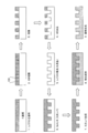
- the present invention it is possible to provide a photocatalyst structure capable of efficiently causing a photocatalytic reaction. Moreover, according to this invention, the novel deodorizing apparatus using this photocatalyst structure can be provided.
- FIG. 4A is a view showing the laminated structure of the purification plate 10
- FIG. 4B is a view showing the uneven structure 11a of the substrate 11, and FIG. It is a figure which shows a next electrophotographic image.
- the purification plate 10 includes a substrate 11, a permeable film 12, a photocatalyst film 13, and an adsorption film 14.
- the substrate 11 is made of a translucent material such as polycarbonate, and the refractive index is set to 1.6.
- a concavo-convex structure 11a is formed such that cylindrical protrusions are arranged at a constant pitch evenly in the vertical and horizontal directions, as shown in FIGS. .
- the pitch of the concavo-convex structure 11a (the width of the columnar protrusion) is 250 nm both vertically and horizontally, and the height of the columnar protrusion is 175 nm.
- the photographic image in FIG. 6C is an image obtained when an alloy film is formed to 20 nm on the concavo-convex structure 11a by sputtering and then imaged with 10 Pt-Pd deposited for electrophotographic imaging. is there.
- a resist is applied on a silicon master by spin coating (step 1).
- the concavo-convex structure with the above pitch is formed by EB drawing (electron beam cutting) (step 2).
- development processing is performed (step 3), and RIE processing is performed (step 4).
- oxygen plasma ashing is performed to remove the remaining resist (step 5). Thereby, an uneven structure is formed on the silicon master (Si master).
- Ni plating is performed on the Si base (step 6) to deposit Ni.
- the deposited Ni layer is peeled off from the Si primaries to produce a stamper (Step 7).
- the stamper is injection-molded (step 8) to produce the substrate 11 (step 9). Thereby, the substrate 11 to which the concavo-convex structure is transferred is formed.
- a light-transmitting material such as polyolefin can be used as the material of the substrate 11 in addition to polycarbonate.
- biodegradable materials such as polylactic acid can be used. When a biodegradable material is used, the environmental load at the time of disposal can be reduced.
- laser beam cutting can be used instead of EB drawing.
- a photoresist layer is applied on the silicon master.
- a laser beam having a wavelength of about 400 nm is used as the cutting beam.
- the permeable film 12 is laminated on the concavo-convex structure 11a of the substrate 11 formed by the above procedure by a sputtering method.
- the transmission film 12 is made of Al 2 O 3 and has a refractive index of 1.6 so as to be substantially the same as that of the substrate 11.
- the upper and lower surfaces of the permeable film 12 have a concavo-convex structure reflecting the concavo-convex structure 11 a of the substrate 11. Since the permeable membrane 12 is made of a non-electrolytic inorganic material, it is not eroded by the photocatalytic reaction of the photocatalytic membrane 13 described later.
- the film thickness and Ra (surface roughness) of the transmission film 12 are set so that the substrate 11 is not eroded by the photocatalyst film 13 and light incident from the substrate 11 side reaches the photocatalyst film 13 sufficiently. ing.
- the substrate 11 is eroded by the photocatalytic reaction of the photocatalyst film 13 and the substrate 11 is deteriorated.
- the film thickness of the permeable film 12 is set large in order to prevent the generation of holes, light incident from the substrate 11 side is absorbed by the permeable film 12 and hardly reaches the photocatalyst film 13. For this reason, the photocatalytic reaction in the photocatalytic film 13 is difficult to proceed.
- the Ra of the permeable membrane 12 is controlled by adjusting the gas pressure during sputtering.
- the film thickness of the permeable film 12 was 7 nm and Ra was 0.8 nm
- the substrate 11 was eroded by the photocatalytic reaction of the photocatalyst film 13, but the film thickness of the permeable film 12 was reduced.
- the thickness was 7 nm and Ra was 0.6 nm
- the substrate 11 was not eroded by the photocatalytic reaction of the photocatalytic film 13. From this, it is judged that it is desirable to form the permeable membrane 12 so that Ra on the membrane surface is about 10% or less of the film thickness.
- the film thickness of the transmission film 12 is preferably set to about 3 to 80 nm so that light incident from the substrate 11 side is sufficiently transmitted toward the photocatalytic film 13. From the above, in this embodiment, the thickness of the permeable membrane 12 is 7 nm and Ra is 0.66.
- the gas pressure during sputtering was 0.3 Pa.
- the photocatalyst film 13 is laminated on the upper surface of the permeable film 12 by sputtering.
- the photocatalytic film 13 is made of TiO 2 and has a refractive index of 2.5.
- the upper and lower surfaces of the photocatalyst film 13 have a concavo-convex structure reflecting the concavo-convex structure formed on the upper surface of the transmission film 12. Thereby, a structure reflecting the concavo-convex structure 11a on the surface of the substrate 11 is formed on the upper surface (reaction surface) of the photocatalyst film 13, the surface area of the upper surface of the photocatalyst film 13 is increased, and a photocatalytic reaction easily occurs.
- the surface of the photocatalyst film 13 itself after film formation can be made porous by adjusting the gas pressure when it is laminated.
- the surface area of the photocatalyst film 13 can be increased, and the surface area of the photocatalyst film 13 can be increased more than the uneven structure 11 a of the substrate 11.
- the film thickness of the photocatalyst film 13 is small, the upper surface of the transmission film 12 is not completely covered by the photocatalyst film 13.
- the film thickness of the photocatalyst film 13 is set to 80 nm so that the upper surface of the permeable film 12 is sufficiently covered and light transmitted to the upper surface is sufficiently obtained. did.
- TiO 2 forming the photocatalytic film 13 includes anatase crystal fine particles.
- the anatase crystal absorbs ultraviolet light having a wavelength of 388 nm or less from the band gap and causes a photocatalytic reaction.
- anatase crystals are fine particles and are present in the photocatalyst film 13, the anatase crystals are uniformly distributed over the substrate 11 even if the shape of the substrate 11 is complicated. Thereby, the photocatalytic reaction easily occurs efficiently over a wide range on the photocatalytic film 13.
- TiO 2 is known to form a rutile structure, an amorphous structure, and a brookite structure in addition to the anatase crystal structure, and the photocatalytic reaction varies depending on the structure. That is, the activity of reaction and the wavelength at which it reacts differ from structure to structure.
- the TiO 2 forming the photocatalytic film 13 used in the present embodiment includes a plurality of structures. Specifically, amorphous and anatase crystal defects, fine particles containing a small amount of nitrogen contained during sputtering, and rutile fine particles are included. Thereby, the photocatalytic reaction of the photocatalytic film 13 is also promoted by light having a wavelength in the visible light region of 400 to 500 nm.
- the structure formed of TiO 2 does not need to include all the structures described above other than the anatase crystal structure, and may include fine particles that can obtain activity with visible light.
- the photocatalytic film 13 exerts a photocatalytic action on the substance attached to the photocatalytic film 13.
- substances that undergo photocatalysis include ammonia, acetaldehyde, hydrogen sulfide, methyl mercaptan, formaldehyde, acetic acid, toluene, fungi, and oil. These substances are decomposed into carbon dioxide, water and the like under the photocatalytic action.
- the adsorption film 14 is laminated on the upper surface of the photocatalyst film 13 by sputtering.
- Adsorption film 14 is formed of SiO 2.
- SiO 2 is hygroscopic and has the property of easily taking in water molecules and gas phase gas in the air. This makes it easier for substances in the air on the upper surface of the adsorption film 14 to adhere to the adsorption film 14. Further, the substance adsorbed on the adsorption film 14 remains on the adsorption film 14 and undergoes photocatalysis.
- the adsorption film 14 is laminated on the photocatalyst film 13 so that the upper surface of the photocatalyst film 13 is not completely coated. That is, countless fine holes are formed in the adsorption film 14 by reducing the gas pressure during sputtering (specifically, 0.8 to 1 Pa or more) or increasing the sputtering rate (70 (/ min or more). Is done. Thereby, the substance adhering to the upper surface of the adsorption film 14 comes into contact with the photocatalyst film 13 through the fine holes.
- the film thickness of the adsorption film 13 is desirably set to a thickness at which the substance attached to the adsorption film 14 efficiently contacts the photocatalytic film 13, and specifically, about 3 to 100 nm is desirable. In the present embodiment, the thickness of the adsorption film 13 is 7 nm.
- the purification plate 10 when ultraviolet light having a wavelength of 375 nm is irradiated from the surface of the substrate 11 opposite to the transmission film 12 (hereinafter referred to as “incident surface”) to the purification plate 10, Such ultraviolet light passes through the substrate 11, the transmission film 12, and the photocatalyst film 13 and reaches the upper surface of the photocatalyst film 13 (hereinafter referred to as “reaction surface”). Thereby, the substance adhering to the adsorption film 14 and in contact with the reaction surface can receive a photocatalytic action.
- the transmission film 12 is disposed between the substrate 11 and the photocatalytic film 13, erosion of the substrate 11 due to the photocatalytic action of the photocatalytic film 12 can be suppressed.
- the concavo-convex structure is formed on the reaction surface, the area where the reaction surface comes into contact with the substance is increased, and the photocatalytic reaction by the photocatalyst film 13 easily occurs.
- the ultraviolet light causes multiple reflection on the surface of the concavo-convex structure formed on the reaction surface, the opportunity for reaction between the photocatalyst film 13 and the ultraviolet light increases, and the photocatalytic reaction by the photocatalyst film 13 easily occurs.
- the photocatalytic reaction with respect to the substance is more efficiently performed than in the case where the adsorption film 14 is not provided.
- a fine concavo-convex structure is formed on the contact surface of the substrate 11 and the permeable film 12, the contact surface of the permeable film 12, and the contact surface of the photocatalyst film 13.
- the refractive index of the transmission film 12 and the substrate 11 is adjusted to 1.6.
- the material of the transmission film 12 and the substrate 11 is appropriately set accordingly. Just choose.
- the materials of the transmission film 12 and the substrate 11 are made to be as close as possible to each other. It is good to choose.
- the purification plate 10 since light can be incident from the incident surface, a photocatalytic reaction can be caused on the reaction surface. Therefore, even when a large amount of the substance to be purified adheres to the adsorption film 14, the reaction surface. The photocatalytic reaction in can occur without delay.
- the permeable film 12, the photocatalyst film 13, and the adsorption film 14 may be arranged not only on the upper surface side of the substrate 11 but also on the lower surface side, similarly to the upper surface side.
- the adsorption film 14 is composed of a light transmission film.
- a single light source causes a photocatalytic reaction on the lower surface (reaction surface) of the permeable film 12 on the lower surface side and the upper surface (reaction surface) of the permeable film 12 on the upper surface side.
- the material used for each layer of the purification plate 10 is not limited to the above.
- the thickness of each layer can also be suitably changed according to the change of material.
- the wavelength of light used for the photocatalytic reaction can be appropriately changed according to the material used for the photocatalytic film 13.
- a concavo-convex structure was formed on the substrate so that cylindrical protrusions were arranged at a constant pitch evenly in the vertical and horizontal directions.
- the pitch of the concavo-convex structure (distance between adjacent cylindrical protrusions) is 250 nm both vertically and horizontally, and the height of the cylindrical protrusion is 170 nm.
- the uneven structure was generated by the process shown in FIG. That is, the substrate on which the concavo-convex structure was transferred was formed by the process shown in FIG. In this measurement, polycarbonate was used as the substrate material.
- the alloy film (reflection film) was formed as follows.
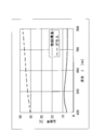
- FIG. 3 shows the measurement results.
- the measurement results of reflectivity for a structure in which an alloy film of Co50Al50at.% Is formed by sputtering on a glass substrate having a flat reflective film forming surface are shown.
- the light was irradiated from the alloy film (reflective film) side so that a plurality of concavo-convex structures were included in the irradiation range.
- the effect of reducing the reflectance occurs when at least the pitch of the concavo-convex structure (250 nm) is smaller than the wavelength of light used for the photocatalytic reaction (375 nm). Therefore, in the purification plate 10, the pitch of the concavo-convex structure is set smaller than the wavelength of light used for the photocatalytic reaction, so that the interface between the substrate 11 and the transmission film 12, the contact surface of the transmission film 12 and the interface between the photocatalyst film 13 The reflection of the light at can be suppressed.
- ⁇ Deodorization device The following is an example in which the purification plate 10 is applied to a deodorizing apparatus.
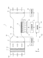
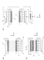
- FIG. 4 is a diagram showing the configuration of the deodorizing apparatus 1.
- the deodorizing apparatus 1 includes a purification plate 10, a blower path 20, fans 31 and 32, filters 41 and 42, an odor sensor 51, a light emitting unit 60, an LED drive circuit 70, and fan drive circuits 81 and 82.
- the power switch 90 and the control circuit 100 are provided.
- the blower path 20 is formed of a hollow cylinder and is configured such that air can flow in the X-axis direction.
- An intake port 20a and an exhaust port 20b are formed at the inlet and the outlet of the air passage 20, respectively.
- a purification region 20 c for arranging the purification plate 10 is formed in the vicinity of the center of the blower path 20.
- the purification plate 10 has the substrate 11, the permeable film 12, the photocatalyst film 13, and the adsorption film 14 laminated so as to be parallel to the XY plane. Moreover, the purification
- the fans 31 and 32 circulate air from the intake port 20a to the exhaust port 20b. Thereby, the air in the vicinity of the intake port 20a is sucked from the intake port 20a by the fan 31, passes through the purification region 20c, and is sent from the exhaust port 20b by the fan 32.
- the filter 41 removes large dust contained in the air sucked from the intake port 20a, and the filter 42 removes small dust contained in the air sent from the filter 41 side.
- the odor sensor 51 detects odor components contained in the air sent from the fan 31 toward the purification region 20c. The detection signal of the odor sensor 51 is output to the control circuit 100.
- the light emitting unit 60 has a plurality of LEDs 61 on the XY plane. These LEDs 61 emit light having a wavelength of 375 nm toward the incident surface of the purification plate 10.
- the LED drive circuit 70 drives the plurality of LEDs 61 arranged in the light emitting unit 60 in response to a command from the control circuit 100.
- the fan drive circuits 81 and 82 drive the fans 31 and 32, respectively, in response to a command from the control circuit 100.
- the number of rotations of the fans 31 and 32 is controlled by the control circuit 100.
- the power switch 90 is provided with an ON / OFF switching switch, and the operator can switch the power of the deodorizing apparatus 1 to ON / OFF by switching the switch.
- a switching signal for the power switch 90 is output to the control circuit 100.
- the control circuit 100 controls the LED drive circuit 70 and the fan drive circuits 81 and 82 based on the output signal of the odor sensor 51 and the switching signal of the power switch 90.
- the deodorizing apparatus 1 When the deodorizing apparatus 1 is configured in this way, the air taken in from the air inlet 20a by driving the fan 31 is removed by the filters 41 and 42 and sent to the purification region 20c.
- the air sent to the purification region 20 c comes into contact with the adsorption film 14 of the purification plate 10, the substance contained in the air is retained by the adsorption film 14 and comes into contact with the reaction surface of the photocatalytic film 13.
- the photocatalytic film 13 is irradiated with light from the LED 61 of the light emitting unit 60, a photocatalytic reaction occurs on the reaction surface, and the substance in contact with the reaction surface is decomposed.
- the substance decomposed by the action of the purification plate 10 is sent out from the purification region 20c toward the exhaust port 20b when the fans 31 and 32 are driven, and is sent out from the exhaust port 20b. In this way, substances contained in the air near the deodorizing device 1 are purified.
- the air flow path and the drive circuit such as the LED 61 can be disposed with the purification plate 10 interposed therebetween, purification can be performed even if the purification substance is a gas that erodes the circuit.
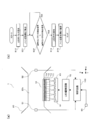
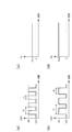
- FIG. 5 is a diagram for explaining control by the control circuit 100.
- FIG. 4A is a flowchart showing the control of the LED 61 and the fans 31 and 32 immediately after the power switch 90 of the deodorizing apparatus 1 is turned on.
- the control circuit 100 causes the LED 61 to emit light in pulses via the LED driving circuit 70 (S12).
- the LED 61 emits pulses
- the LED 61 is turned on (lit) for a time t1 every period T1, as shown in FIG.
- the control circuit 100 causes the LED 61 to emit DC light via the LED drive circuit 70.
- the LED 61 emits DC light
- the LED 61 is always ON (lighted) as shown in FIG.
- the control circuit 100 drives the fans 31 and 32 via the fan drive circuits 81 and 82. In this way, the deodorizing apparatus 1 is operated normally.
- the power of the deodorizing apparatus 1 is turned on and the LED 61 emits DC light
- the photocatalyst film 13 absorbs light energy, and the temperature of the photocatalyst film 13 rises suddenly.
- the adhering unpurified substance is released into the air in the purification region 20c without being purified.
- the fans 31 and 32 are driven in this state, unpurified substances released into the air in the purification region 20c are sent out from the exhaust port 20b.
- the unpurified substance is separated from the adsorption film 14 by the airflow generated by the fans 31 and 32 and is sent out from the exhaust port 20b.
- the LED 61 emits pulse light for a certain period after the power is turned on. Therefore, the temperature rise of the photocatalyst film 13 during this period is moderate. For this reason, the unpurified substance adhering to the adsorption film 14 is retained on the adsorption film 14 and purified. Thereby, it is suppressed that an unpurified substance is discharge
- the fans 31 and 32 are stopped, unpurified substances adhering to the adsorption film 14 are prevented from being separated from the adsorption film 14 and sent out from the exhaust port 20b by the air flow. obtain. Although the fans 31 and 32 are stopped here, the fans 31 and 32 are driven at a low rotational speed (weak operation) to such an extent that unpurified substances adhering to the adsorption film 14 are not released into the air. ).
- the predetermined time used for the determination in S13 is the time required until the unpurified substance adhering to the adsorption film 14 is sufficiently reduced, that is, necessary for purifying to the extent that new adsorption is possible. Set to required time. In this way, after a predetermined time has elapsed, the unpurified substance adhering to the adsorption film 14 is reduced, and the substance floating in the purification region 20c can be adsorbed to the adsorption film 14. Therefore, the deodorizing apparatus can be quickly used. Air intake in the vicinity of 1 can be started.
- FIG. 5B is a flowchart showing the control of the LED 61 during the normal operation of the deodorizing apparatus 1.
- the LED 61 When the control circuit 100 determines that the detection signal of the odor sensor 51 is equal to or less than the predetermined value (S21: YES), the LED 61 emits pulses (S22), and determines that the detection signal of the odor sensor 51 is larger than the predetermined value. (S21: NO), the LED 61 is caused to emit DC light (S23).
- the purification target substance can be reliably purified even when a very small amount of the substance to be purified exists in the air sent to the purification region 20c. Is possible. That is, when the LED 61 emits DC light when there is only a trace amount of the purification target substance in the air, the temperature of the photocatalytic film 13 rises. Thereby, since the temperature of the air in the vicinity of the purification plate 10 rises, the purification target substance contained in the air becomes difficult to adhere to the adsorption film 14, and the purification target substance becomes difficult to be purified. However, in this case, if the LED 61 emits pulses, the temperature increase of the photocatalytic film 13 is suppressed, so that the purification target substance is likely to adhere to the adsorption film 14 and the purification target substance is easily purified.
- the substance contained in the air sucked from the intake port 20a is purified by the photocatalytic action of the photocatalyst film 13 of the purification plate 10 and is sent out from the exhaust port 20b. Thereby, the air near the deodorizing apparatus 1 can be purified.
- the deodorizing apparatus 1 even after the deodorizing apparatus 1 is turned on, the unpurified substance attached to the adsorption film 14 when the power is turned off can be sent out from the exhaust port 20b. Since it is suppressed, it is possible to suppress the odor from being emitted from the deodorizing apparatus 1 to the outside immediately after the power is turned on. Further, when the purification target substance is in a very small amount during normal operation of the deodorizing apparatus 1, the LED 61 emits pulse light and the temperature rise of the photocatalytic film 13 is suppressed. 10 and can be purified more reliably.
- Fig.6 (a) is a figure which shows the structure of the deodorizing apparatus 1 in this example of a change.
- the deodorizing apparatus 1 in this modified example has a configuration in which an odor sensor 52 is added to the deodorizing apparatus 1 shown in FIG.
- the odor sensor 52 has the same configuration as that of the odor sensor 51 and detects an odor component contained in the air sent from the purification region 20 c toward the fan 32.
- the detection signal of the odor sensor 52 is output to the control circuit 100.
- FIG. 6A only the vicinity of the purification region 20c is shown for convenience.
- FIG. 6B is a flowchart showing control of the LED 61 and the fans 31 and 32 immediately after the deodorizing apparatus 1 is turned on.
- S11 and S13 are deleted and S31 and S32 are added from the flowchart of FIG.
- the control circuit 100 causes the LED 61 to emit pulses via the LED driving circuit 70 (S12), and drives the fans 31 and 32 at a rotational speed that is several steps lower than the normal state ( Drive weakly).
- the control circuit 100 determines whether or not the detection signal of the odor sensor 51 is larger than the detection signal of the odor sensor 52 (S32). If it is determined that the detection signal of the odor sensor 51 is larger than the detection signal of the odor sensor 52 (S32: YES), the process proceeds to S14 and S15, and the drive of the LED 61 and the fans 31, 32 is in the normal state. Is done. On the other hand, if it is determined that the detection signal of the odor sensor 51 is equal to or less than the detection signal of the odor sensor 52 (S32: NO), the process waits.
- the control circuit 100 causes the deodorizing device 1 to It is determined that the unpurified substance adhering to the adsorption film 14 is substantially purified when the power is turned off, and the LED 61 and the fans 31 and 32 are driven in a normal state (S14 and S15).
- the purification plate 10 is not limited to the arrangement shown in FIGS. 4 and 6A, and another purification plate similar to the purification plate 10 may be arranged as follows. In FIG. 7, only the vicinity of the purification region 20 c is shown for convenience.
- a purification plate 110 is installed so as to be symmetrical with the purification plate 10 shown in FIGS. 4 and 6A with respect to the purification region 20c.
- the light emitted from the LED 61 is absorbed by the purification plate 10. Further, the light transmitted through the purification plate 10 is absorbed by the adsorption film 14 of the purification plate 110 and the substance attached on the adsorption film 14 of the purification plate 110. However, part of the light emitted from the LED 61 reaches the photocatalytic film 13 of the purification plate 110 and causes a photocatalytic reaction in the photocatalytic film 13 of the purification plate 110. Thereby, the air in the purification
- another purification plate 110 may be installed on the inner wall surface of the purification region 20c between the purification plate 10 and the purification plate 110.
- another purification plate 120 is arranged in the positive direction of the Z-axis of the purification plate 10 shown in FIGS. 4 and 6 (a).
- the permeable film 12, the photocatalyst film 13, and the adsorption film 14 are arranged so as to have a photocatalytic action on both surfaces in the positive and negative directions of the Z axis.
- cleaning board 120 is being fixed to the inner wall face of the purification
- the light emitted from the LED 61 passes through the purification plate 10 and reaches the photocatalytic film 13 in both the positive and negative directions of the Z-axis of the purification plate 120, and a photocatalytic reaction occurs in each photocatalytic film 13.
- the air in the purification region 20c can be further purified by greatly increasing the reaction area with one light source.
- another purification plate having the same configuration as the purification plate 120 may be installed in the positive direction of the Z axis of the purification plate 120 in the purification region 20 c.
- the purification plate 110 and the light emission are symmetric with respect to the purification region 20c so as to be symmetric with the purification plate 10 and the light emitting unit 60 shown in FIGS.
- a unit 130 is installed.
- the light emitting unit 130 has the same configuration as that of the light emitting unit 60, and the light emitted from the plurality of LEDs 61 arranged in the light emitting unit 130 is irradiated to the photocatalyst film 13 of the purification plate 110.
- the light from the light emitting unit 60 passes through the purification plate 10 and reaches the purification plate 110. Further, the light from the light emitting unit 130 passes through the purification plate 110 and reaches the purification plate 10. Thereby, the light quantity irradiated to the reaction surface of the photocatalyst film
- the air in the purification region 20c can be further purified as compared with the embodiment of the deodorizing apparatus.
- the purification plate and the light emitting unit are arranged to face each other in the Z-axis direction.
- the purification plate and the light emitting unit may be arranged to face each other in the Y-axis direction. In this way, the air in the purification region 20c can be further purified.
- the purification plate 120 in FIG. 7B may be disposed between the purification plate 10 and the purification plate 110. In this way, since the light transmitted through the purification plates 10 and 110 is irradiated onto the purification plate 120 from above and below, the photocatalytic reaction on the upper and lower surfaces of the purification plate 120 can be performed efficiently.
- the purification plates are configured in multiple stages from the light emitting unit in the light emitting direction, the number of light emitting units can be reduced as much as possible, and the cost can be reduced. Moreover, since the light which permeate
- the purification plate 10 includes the substrate 11, the permeable film 12, the photocatalytic film 13, and the adsorption film 14 so as to be formed with a transmittance of 70% or more.
- a transmitted light of 25% or more was obtained even in a four-layer structure, and it functioned sufficiently even if there was a loss of light.
- the transmittance is at least 50% for the purification plate alone.
- the light emission state of the LED 61 is pulse light emission or DC light emission, but the LED 61 is controlled so that the light emission energy of the LED 61 changes stepwise according to the detection signal of the odor sensor 51. May be.
- the light energy reaching the photocatalyst film 13 can be changed according to the amount of the substance to be purified contained in the purification region 20c, so that a photocatalytic reaction can be more efficiently caused.
- the LED 61 only needs to emit light at a period T2 different from the period T1 of FIG.
- the LED 61 may emit light with a light emission time different from the light emission time t1 of FIG.
- the LED 61 is used as a light source for causing a photocatalytic reaction.
- a semiconductor laser may be used instead of the LED 61.
- the light energy applied to the photocatalytic film 13 is adjusted by switching the semiconductor laser to DC light emission or pulse light emission as in the above embodiment.
- the light energy applied to the photocatalyst 13 may be adjusted by switching the emission power of the semiconductor laser between Pw1 and Pw2.
- the emission power Pw of the semiconductor laser may be changed stepwise.
- the semiconductor laser has a wide range of output power, which is advantageous for changing in steps.
- Claim 4 which concerns on the deodorizing apparatus of this invention can be characterized by the following restrictions other than the claim as described in a claim.
- the deodorization apparatus further comprising an odor sensor disposed in a ventilation path for flowing the air through the photocatalyst structure, wherein the light source has a detection signal equal to or lower than a predetermined value.
- the light is emitted from the light source at a first power, and when the detection signal of the odor sensor is larger than a predetermined value, the light is emitted from the light source at a second power larger than the first power.
- Deodorizing device characterized by.
- the deodorizing apparatus further comprising first and second odor sensors respectively disposed on an upstream side and a downstream side of the photocatalyst structure, wherein when the deodorizing apparatus is activated, the fan has a first odor sensor.
- the detection signal of the first odor sensor becomes larger than the detection signal of the second odor sensor after the activation.
- the fan is driven at a second rotational speed larger than the first rotational speed, and the light is emitted from the light source at a second power larger than the first power.
- Deodorizing device When the light is emitted at a first power from the light source and driven at a rotational speed, and the detection signal of the first odor sensor becomes larger than the detection signal of the second odor sensor after the activation.
- the fan is driven at a second rotational speed larger than the first rotational speed, and the light is emitted from the light source at a second power larger than the first power.
Landscapes
- Chemical & Material Sciences (AREA)
- Engineering & Computer Science (AREA)
- Chemical Kinetics & Catalysis (AREA)
- Materials Engineering (AREA)
- Organic Chemistry (AREA)
- Health & Medical Sciences (AREA)
- Environmental & Geological Engineering (AREA)
- Physics & Mathematics (AREA)
- Epidemiology (AREA)
- General Chemical & Material Sciences (AREA)
- Public Health (AREA)
- Veterinary Medicine (AREA)
- Animal Behavior & Ethology (AREA)
- Biomedical Technology (AREA)
- Analytical Chemistry (AREA)
- General Health & Medical Sciences (AREA)
- Oil, Petroleum & Natural Gas (AREA)
- Life Sciences & Earth Sciences (AREA)
- Optics & Photonics (AREA)
- Plasma & Fusion (AREA)
- Toxicology (AREA)
- Catalysts (AREA)
- Exhaust Gas Treatment By Means Of Catalyst (AREA)
- Disinfection, Sterilisation Or Deodorisation Of Air (AREA)
Abstract
Description
図1に、本実施の形態に係る浄化板10の構成を示す。同図(a)は、浄化板10の積層構造を示す図であり、同図(b)は、基板11の凹凸構造11aを示す図であり、同図(c)は、凹凸構造11aの二次電子写真像を示す図である。
発明者は、上記凹凸構造による反射率低減作用の測定を行ったので、以下、これについて説明する。
以下は、上記浄化板10を脱臭装置に適用した例である。
図6(a)は、本変更例における脱臭装置1の構成を示す図である。
上記浄化板10は、図4と図6(a)に示したような配置に限られず、以下のように、浄化板10と同様の別の浄化板が配置されても良い。なお、図7では、便宜上、浄化領域20cの近傍のみ図示されている。
11 … 基板
12 … 透過膜
13 … 光触媒膜
14 … 吸着膜
31、32 … ファン
51、52 … 臭気センサ
60、130 … 発光ユニット(光源)
61 … LED(光源)
Claims (6)
- 凹凸構造が表面に形成された基板と、
前記基板の前記凹凸構造側に配されるとともに前記凹凸構造の形状が反映された光触媒膜と、を備え、
前記凹凸構造は、前記光触媒膜が光触媒反応を起こす光の波長よりも小さいピッチで形成されている、
ことを特徴とする光触媒構造体。 - 請求項1に記載の光触媒構造体において、
前記基板と前記光触媒膜との間に透過膜をさらに備える、
ことを特徴とする光触媒構造体。 - 請求項1または2に記載の光触媒構造体において、
前記光触媒膜上に配されるとともに物質を滞留させて前記光触媒膜に接触させる吸着膜をさらに備える、
ことを特徴とする光触媒構造体。 - 請求項1ないし3の何れか一項に記載の光触媒構造体と、
前記光を前記基板側から前記光触媒構造体に照射する光源と、
前記光触媒構造体に空気を流すためのファンと、を備える、
ことを特徴とする脱臭装置。 - 請求項4に記載の脱臭装置において、
前記脱臭装置の起動時には、前記光源から第1のパワーで前記光が出射され、
前記起動から所定の時間が経過すると、前記光源から前記第1のパワーよりも大きい第2のパワーで前記光が出射される、
ことを特徴とする脱臭装置。 - 請求項4または5に記載の脱臭装置において、
前記光触媒構造体に前記空気を流すための送風経路内に配された臭気センサをさらに備え、
前記臭気センサからの検出信号に基づいて前記光源からの光の出射パワーが制御される、
ことを特徴とする脱臭装置。
Priority Applications (2)
| Application Number | Priority Date | Filing Date | Title |
|---|---|---|---|
| CN2010800488301A CN102596410A (zh) | 2009-10-30 | 2010-08-24 | 光催化剂构造体以及除臭装置 |
| US13/505,256 US20120219459A1 (en) | 2009-10-30 | 2010-08-24 | Photocatalytic structural member and deodorizing device |
Applications Claiming Priority (2)
| Application Number | Priority Date | Filing Date | Title |
|---|---|---|---|
| JP2009249907A JP2011092873A (ja) | 2009-10-30 | 2009-10-30 | 光触媒構造体および脱臭装置 |
| JP2009-249907 | 2009-10-30 |
Publications (1)
| Publication Number | Publication Date |
|---|---|
| WO2011052286A1 true WO2011052286A1 (ja) | 2011-05-05 |
Family
ID=43921716
Family Applications (1)
| Application Number | Title | Priority Date | Filing Date |
|---|---|---|---|
| PCT/JP2010/064223 Ceased WO2011052286A1 (ja) | 2009-10-30 | 2010-08-24 | 光触媒構造体および脱臭装置 |
Country Status (4)
| Country | Link |
|---|---|
| US (1) | US20120219459A1 (ja) |
| JP (1) | JP2011092873A (ja) |
| CN (1) | CN102596410A (ja) |
| WO (1) | WO2011052286A1 (ja) |
Families Citing this family (15)
| Publication number | Priority date | Publication date | Assignee | Title |
|---|---|---|---|---|
| JP6021348B2 (ja) * | 2012-02-16 | 2016-11-09 | 東芝ライフスタイル株式会社 | 冷蔵庫 |
| JP6165556B2 (ja) * | 2013-08-27 | 2017-07-19 | スタンレー電気株式会社 | 水素製造装置 |
| KR102627891B1 (ko) | 2018-01-22 | 2024-01-23 | 서울바이오시스 주식회사 | 탈취 모듈 및 이를 구비하는 건조 장치 |
| US11881093B2 (en) | 2020-08-20 | 2024-01-23 | Denso International America, Inc. | Systems and methods for identifying smoking in vehicles |
| US12377711B2 (en) | 2020-08-20 | 2025-08-05 | Denso International America, Inc. | Vehicle feature control systems and methods based on smoking |
| US11932080B2 (en) | 2020-08-20 | 2024-03-19 | Denso International America, Inc. | Diagnostic and recirculation control systems and methods |
| US12269315B2 (en) | 2020-08-20 | 2025-04-08 | Denso International America, Inc. | Systems and methods for measuring and managing odor brought into rental vehicles |
| US12017506B2 (en) | 2020-08-20 | 2024-06-25 | Denso International America, Inc. | Passenger cabin air control systems and methods |
| US11636870B2 (en) | 2020-08-20 | 2023-04-25 | Denso International America, Inc. | Smoking cessation systems and methods |
| US11828210B2 (en) | 2020-08-20 | 2023-11-28 | Denso International America, Inc. | Diagnostic systems and methods of vehicles using olfaction |
| US11760169B2 (en) | 2020-08-20 | 2023-09-19 | Denso International America, Inc. | Particulate control systems and methods for olfaction sensors |
| US11760170B2 (en) | 2020-08-20 | 2023-09-19 | Denso International America, Inc. | Olfaction sensor preservation systems and methods |
| US11813926B2 (en) | 2020-08-20 | 2023-11-14 | Denso International America, Inc. | Binding agent and olfaction sensor |
| US12251991B2 (en) | 2020-08-20 | 2025-03-18 | Denso International America, Inc. | Humidity control for olfaction sensors |
| JP7767187B2 (ja) * | 2022-03-09 | 2025-11-11 | シャープ株式会社 | 除菌脱臭機、制御プログラムおよび制御方法 |
Citations (5)
| Publication number | Priority date | Publication date | Assignee | Title |
|---|---|---|---|---|
| JP2000006303A (ja) * | 1998-06-25 | 2000-01-11 | Akira Fujishima | 光触媒層を有する積層構造体 |
| JP2000126609A (ja) * | 1998-10-28 | 2000-05-09 | Mitsubishi Paper Mills Ltd | 光触媒コルゲート構造体およびそれを用いた光触媒脱臭部材、光触媒脱臭装置 |
| JP2004252130A (ja) * | 2003-02-20 | 2004-09-09 | Sanyo Electric Co Ltd | 表面微細構造光学素子およびその製造方法 |
| JP2006255701A (ja) * | 2006-03-28 | 2006-09-28 | Toyoda Gosei Co Ltd | 光触媒装置 |
| JP2008295936A (ja) * | 2007-06-04 | 2008-12-11 | Toshiba Corp | 脱臭装置 |
Family Cites Families (2)
| Publication number | Priority date | Publication date | Assignee | Title |
|---|---|---|---|---|
| US6783740B2 (en) * | 2002-09-30 | 2004-08-31 | Northrop Grumman Corporation | Sintered glass bead filter with active microbial destruction |
| US20090004066A1 (en) * | 2007-06-30 | 2009-01-01 | Yu-Lin Cheng | Air purifier with a sensor and/or timer switching function. |
-
2009
- 2009-10-30 JP JP2009249907A patent/JP2011092873A/ja not_active Withdrawn
-
2010
- 2010-08-24 WO PCT/JP2010/064223 patent/WO2011052286A1/ja not_active Ceased
- 2010-08-24 US US13/505,256 patent/US20120219459A1/en not_active Abandoned
- 2010-08-24 CN CN2010800488301A patent/CN102596410A/zh active Pending
Patent Citations (5)
| Publication number | Priority date | Publication date | Assignee | Title |
|---|---|---|---|---|
| JP2000006303A (ja) * | 1998-06-25 | 2000-01-11 | Akira Fujishima | 光触媒層を有する積層構造体 |
| JP2000126609A (ja) * | 1998-10-28 | 2000-05-09 | Mitsubishi Paper Mills Ltd | 光触媒コルゲート構造体およびそれを用いた光触媒脱臭部材、光触媒脱臭装置 |
| JP2004252130A (ja) * | 2003-02-20 | 2004-09-09 | Sanyo Electric Co Ltd | 表面微細構造光学素子およびその製造方法 |
| JP2006255701A (ja) * | 2006-03-28 | 2006-09-28 | Toyoda Gosei Co Ltd | 光触媒装置 |
| JP2008295936A (ja) * | 2007-06-04 | 2008-12-11 | Toshiba Corp | 脱臭装置 |
Also Published As
| Publication number | Publication date |
|---|---|
| CN102596410A (zh) | 2012-07-18 |
| US20120219459A1 (en) | 2012-08-30 |
| JP2011092873A (ja) | 2011-05-12 |
Similar Documents
| Publication | Publication Date | Title |
|---|---|---|
| JP2011092873A (ja) | 光触媒構造体および脱臭装置 | |
| JP2013027665A (ja) | 浄化ユニットおよび脱臭装置 | |
| CN102091341B (zh) | 空气净化设备及其形成方法 | |
| CN1886190A (zh) | 改进的光催化氧化空气净化系统 | |
| WO2012023319A1 (ja) | 浄化ユニットおよび脱臭装置 | |
| JP2009247546A (ja) | 空気浄化フィルターおよび空気浄化装置 | |
| KR101249885B1 (ko) | 플라즈몬을 이용한 광촉매 정수장치 | |
| JP2011110518A (ja) | 脱臭装置 | |
| KR102659262B1 (ko) | 반사막이 구비된 공기정화장치 및 그 제조방법 | |
| JP2014117631A (ja) | 光触媒構造体、浄化ユニットおよび浄化装置 | |
| JP4787253B2 (ja) | アルミナ被膜形成方法及びアルミナ繊維並びに同アルミナ繊維を備えたガス処理装置 | |
| GB2424598A (en) | Photocatalyst composition | |
| CN1960769A (zh) | 有害物质的分解方法及有害物质分解装置 | |
| KR102406939B1 (ko) | 마이크로리소그래피용 광학 시스템 | |
| JP2000286187A (ja) | 露光装置、該露光装置に用いるマスク構造体、露光方法、前記露光装置を用いて作製された半導体デバイス、および半導体デバイス製造方法 | |
| JP4354938B2 (ja) | 表面処理方法および表面処理用装置 | |
| JP4830547B2 (ja) | パターン形成体の製造方法およびパターン形成体製造用装置 | |
| JP2006216574A (ja) | 光触媒ledデバイスおよび光触媒ledデバイスモジュール | |
| TWM597148U (zh) | 紫外光光觸媒殺菌器 | |
| KR20050072822A (ko) | 공기 정화 장치 | |
| JPH094900A (ja) | TiO2 の光触媒作用を利用したレンジフード | |
| TWM545785U (zh) | 光觸媒濾淨模組及其光觸媒結構 | |
| JP4951863B2 (ja) | 光触媒含有層付基板、およびその製造方法 | |
| JP2005007300A (ja) | 光触媒反応装置 | |
| JP2002291852A (ja) | 流体浄化装置 |
Legal Events
| Date | Code | Title | Description |
|---|---|---|---|
| WWE | Wipo information: entry into national phase |
Ref document number: 201080048830.1 Country of ref document: CN |
|
| 121 | Ep: the epo has been informed by wipo that ep was designated in this application |
Ref document number: 10826421 Country of ref document: EP Kind code of ref document: A1 |
|
| NENP | Non-entry into the national phase |
Ref country code: DE |
|
| WWE | Wipo information: entry into national phase |
Ref document number: 13505256 Country of ref document: US |
|
| 122 | Ep: pct application non-entry in european phase |
Ref document number: 10826421 Country of ref document: EP Kind code of ref document: A1 |