WO2011043188A1 - 表示方法、表示装置、光学ユニット、表示装置の製造方法、及び電子機器 - Google Patents
表示方法、表示装置、光学ユニット、表示装置の製造方法、及び電子機器 Download PDFInfo
- Publication number
- WO2011043188A1 WO2011043188A1 PCT/JP2010/066380 JP2010066380W WO2011043188A1 WO 2011043188 A1 WO2011043188 A1 WO 2011043188A1 JP 2010066380 W JP2010066380 W JP 2010066380W WO 2011043188 A1 WO2011043188 A1 WO 2011043188A1
- Authority
- WO
- WIPO (PCT)
- Prior art keywords
- display device
- light
- pupil
- light emission
- lens
- Prior art date
Links
- 238000000034 method Methods 0.000 title claims abstract description 35
- 230000003287 optical effect Effects 0.000 title claims description 16
- 238000004519 manufacturing process Methods 0.000 title claims description 15
- 230000004907 flux Effects 0.000 claims abstract description 165
- 210000001747 pupil Anatomy 0.000 claims abstract description 141
- 239000004973 liquid crystal related substance Substances 0.000 claims description 23
- 238000003384 imaging method Methods 0.000 claims description 6
- 239000000463 material Substances 0.000 claims description 4
- 238000009826 distribution Methods 0.000 description 18
- 239000011521 glass Substances 0.000 description 17
- 201000010041 presbyopia Diseases 0.000 description 16
- 230000000694 effects Effects 0.000 description 13
- 238000002438 flame photometric detection Methods 0.000 description 9
- 239000000203 mixture Substances 0.000 description 7
- 238000003491 array Methods 0.000 description 5
- 230000004304 visual acuity Effects 0.000 description 5
- 230000005540 biological transmission Effects 0.000 description 4
- 230000004438 eyesight Effects 0.000 description 3
- 239000011159 matrix material Substances 0.000 description 3
- 238000012856 packing Methods 0.000 description 3
- 230000015572 biosynthetic process Effects 0.000 description 2
- 230000015556 catabolic process Effects 0.000 description 2
- 230000007423 decrease Effects 0.000 description 2
- 238000001962 electrophoresis Methods 0.000 description 2
- 239000011859 microparticle Substances 0.000 description 2
- 208000001491 myopia Diseases 0.000 description 2
- 230000004379 myopia Effects 0.000 description 2
- 230000011514 reflex Effects 0.000 description 2
- VYZAMTAEIAYCRO-UHFFFAOYSA-N Chromium Chemical compound [Cr] VYZAMTAEIAYCRO-UHFFFAOYSA-N 0.000 description 1
- 206010020675 Hypermetropia Diseases 0.000 description 1
- 230000032683 aging Effects 0.000 description 1
- 201000009310 astigmatism Diseases 0.000 description 1
- 229910052804 chromium Inorganic materials 0.000 description 1
- 239000011651 chromium Substances 0.000 description 1
- 238000006073 displacement reaction Methods 0.000 description 1
- 238000005530 etching Methods 0.000 description 1
- 230000004305 hyperopia Effects 0.000 description 1
- 201000006318 hyperopia Diseases 0.000 description 1
- 238000003825 pressing Methods 0.000 description 1
- 230000035945 sensitivity Effects 0.000 description 1
- 239000007779 soft material Substances 0.000 description 1
- 239000012780 transparent material Substances 0.000 description 1
Images


Classifications
-
- G—PHYSICS
- G09—EDUCATION; CRYPTOGRAPHY; DISPLAY; ADVERTISING; SEALS
- G09F—DISPLAYING; ADVERTISING; SIGNS; LABELS OR NAME-PLATES; SEALS
- G09F9/00—Indicating arrangements for variable information in which the information is built-up on a support by selection or combination of individual elements
- G09F9/30—Indicating arrangements for variable information in which the information is built-up on a support by selection or combination of individual elements in which the desired character or characters are formed by combining individual elements
- G09F9/33—Indicating arrangements for variable information in which the information is built-up on a support by selection or combination of individual elements in which the desired character or characters are formed by combining individual elements being semiconductor devices, e.g. diodes
-
- G—PHYSICS
- G09—EDUCATION; CRYPTOGRAPHY; DISPLAY; ADVERTISING; SEALS
- G09F—DISPLAYING; ADVERTISING; SIGNS; LABELS OR NAME-PLATES; SEALS
- G09F9/00—Indicating arrangements for variable information in which the information is built-up on a support by selection or combination of individual elements
- G09F9/30—Indicating arrangements for variable information in which the information is built-up on a support by selection or combination of individual elements in which the desired character or characters are formed by combining individual elements
- G09F9/302—Indicating arrangements for variable information in which the information is built-up on a support by selection or combination of individual elements in which the desired character or characters are formed by combining individual elements characterised by the form or geometrical disposition of the individual elements
- G09F9/3026—Video wall, i.e. stackable semiconductor matrix display modules
-
- G—PHYSICS
- G02—OPTICS
- G02F—OPTICAL DEVICES OR ARRANGEMENTS FOR THE CONTROL OF LIGHT BY MODIFICATION OF THE OPTICAL PROPERTIES OF THE MEDIA OF THE ELEMENTS INVOLVED THEREIN; NON-LINEAR OPTICS; FREQUENCY-CHANGING OF LIGHT; OPTICAL LOGIC ELEMENTS; OPTICAL ANALOGUE/DIGITAL CONVERTERS
- G02F1/00—Devices or arrangements for the control of the intensity, colour, phase, polarisation or direction of light arriving from an independent light source, e.g. switching, gating or modulating; Non-linear optics
- G02F1/01—Devices or arrangements for the control of the intensity, colour, phase, polarisation or direction of light arriving from an independent light source, e.g. switching, gating or modulating; Non-linear optics for the control of the intensity, phase, polarisation or colour
- G02F1/13—Devices or arrangements for the control of the intensity, colour, phase, polarisation or direction of light arriving from an independent light source, e.g. switching, gating or modulating; Non-linear optics for the control of the intensity, phase, polarisation or colour based on liquid crystals, e.g. single liquid crystal display cells
- G02F1/133—Constructional arrangements; Operation of liquid crystal cells; Circuit arrangements
- G02F1/1333—Constructional arrangements; Manufacturing methods
- G02F1/1335—Structural association of cells with optical devices, e.g. polarisers or reflectors
- G02F1/133504—Diffusing, scattering, diffracting elements
-
- G—PHYSICS
- G02—OPTICS
- G02F—OPTICAL DEVICES OR ARRANGEMENTS FOR THE CONTROL OF LIGHT BY MODIFICATION OF THE OPTICAL PROPERTIES OF THE MEDIA OF THE ELEMENTS INVOLVED THEREIN; NON-LINEAR OPTICS; FREQUENCY-CHANGING OF LIGHT; OPTICAL LOGIC ELEMENTS; OPTICAL ANALOGUE/DIGITAL CONVERTERS
- G02F1/00—Devices or arrangements for the control of the intensity, colour, phase, polarisation or direction of light arriving from an independent light source, e.g. switching, gating or modulating; Non-linear optics
- G02F1/01—Devices or arrangements for the control of the intensity, colour, phase, polarisation or direction of light arriving from an independent light source, e.g. switching, gating or modulating; Non-linear optics for the control of the intensity, phase, polarisation or colour
- G02F1/13—Devices or arrangements for the control of the intensity, colour, phase, polarisation or direction of light arriving from an independent light source, e.g. switching, gating or modulating; Non-linear optics for the control of the intensity, phase, polarisation or colour based on liquid crystals, e.g. single liquid crystal display cells
- G02F1/133—Constructional arrangements; Operation of liquid crystal cells; Circuit arrangements
- G02F1/1333—Constructional arrangements; Manufacturing methods
- G02F1/1335—Structural association of cells with optical devices, e.g. polarisers or reflectors
- G02F1/133526—Lenses, e.g. microlenses or Fresnel lenses
Definitions
- the present invention relates to a display method, a display device, an optical unit, a method of manufacturing the display device, and an electronic apparatus equipped with the display device.
- liquid crystal displays and plasma displays as display devices (displays) for displaying images and characters.
- these display devices can not adjust the diopter.
- a display device capable of adjusting the diopter in particular, a flat panel display (as appropriate, referred to as "FPD" is desired.
- FPDs are used as live view monitors in digital single-lens reflex cameras.
- a digital single-lens reflex camera it is not practical to put on and off reading glasses each time to look at a live view monitor while looking at a distant subject.
- Patent Document 1 proposes a method of displaying a corrected image subjected to edge emphasis. Further, Patent Document 2 proposes a method of using a pre-corrected image generated by the inverse matrix of the Toeplitz matrix. Further, Patent Document 3 proposes a method using a loupe.
- Patent No. 3552413 gazette Japanese Patent Application Publication No. 2007-128355 JP, 2009-63624, A
- Patent Document 3 shows a configuration example in which a Fresnel lens is attached in front of an FPD that is a monitor of a digital camera and the FPD is looked like a loupe.
- FPD Fresnel lens
- the present invention has been made in view of the above, and provides a display method in which the focus can be easily adjusted, a display device using the same, an optical unit, a method of manufacturing the display device, and an electronic device equipped with the display device.
- the purpose is to
- a display method for forming an image using a plurality of pixels comprising: Project luminous flux from multiple pixels onto the pupil of the observer's eye, It is possible to provide a display method characterized in that the diameter of the light beam incident on the pupil is smaller than the diameter of the pupil.
- light emitted from one pixel is projected as a plurality of luminous fluxes separated from each other, It is desirable that at least one light flux of the plurality of light fluxes be incident on the pupil of the observer's eye.
- the light emission point be arranged such that one or more and four or less of the plurality of light beams enter the pupil of the observer.
- the diameter of the light beam incident on the observer's pupil be 0.5 mm to 2 mm.
- the light emission point be projected by the lens 200 mm or more beyond the position of the lens.
- an angle formed by the closest light fluxes is 0.58 degrees or less.
- the plurality of light emission points be formed using a mask having a plurality of openings.
- a display device for displaying an image having a plurality of pixels A plurality of light emission points are formed corresponding to each pixel, It is possible to provide a display characterized in that a microlens array having a lens corresponding to each pixel is provided.
- a display device for displaying an image having a plurality of pixels A plurality of light emission points are formed in each pixel, It is possible to provide a display device characterized in that a microlens array is provided having a lens for forming light emitted from a light emission point into a plurality of light beams.
- the plurality of pixel arrays be an array of images to be displayed.
- the diameter of the light flux from the plurality of light emission points be smaller than the diameter of the pupil of the observer's eye.
- the light emission point be arranged such that one or more and four or less of the plurality of light beams enter the pupil of the observer.
- the distance between the light emission points is desirably greater than twice the size of the light emission point.
- the diameter of the light beam incident on the pupil of the observer using the display device be 0.5 mm to 2 mm.
- the light emission point it is desirable to project the light emission point to the position of the pupil of the eye of the observer using the display device by the microlens array.
- the light emission point be projected by the lens to a distance of 200 mm or more than the position of the lens.
- the size of each lens of the microlens array is desirably 50 to 500 ⁇ m.
- the size of the pixel is preferably 500 ⁇ m or less.
- the plurality of light emission points be configured by an opening.
- the opening is preferably provided on the mask.
- the mask is preferably provided at a position closer to the microlens than the position of the pixel.
- the pixel is made of liquid crystal.
- the mask be disposed at a position closer to the light guide plate than the position of the liquid crystal.
- the surface on the light guide plate side of the mask be constituted by a reflective surface.
- the pixel is configured of an organic EL device.
- a microlens array comprising a plurality of microlenses, And a mask having a plurality of apertures corresponding to each one of the lenses.
- the mask is desirably formed integrally with the microlens array.
- the lens projects the image of the mask 200 mm or more away from the lens.
- the size of the lens is desirably 50 to 500 ⁇ m.
- the microlens array is desirably made of a flexible material.
- the microlens array is desirably formed by nanoimprinting.
- the diameter of the light flux from the plurality of light emission points be smaller than the diameter of the pupil of the eye of the observer using the display device.
- the light emission points are arranged such that one or more and four or less of the light fluxes of the plurality of light emission points are incident on the pupil of the observer. Is desirable.
- the diameter of the light beam incident on the pupil of the observer using the display device be 0.5 mm to 2 mm.
- the light emission point be projected by the lens to a distance of 200 mm or more than the position of the lens.
- the size of the lens is desirably 50 to 500 ⁇ m.
- an imaging device including the above-described display device.
- the present invention has the effect of being able to provide a display method with which focus is easily achieved, a display device using the same, an optical unit, a method of manufacturing the display device, and an electronic device equipped with the display device.
- FIG. 7 is yet another view of the depth of field. It is a figure explaining the basic concept of a display method, and the basic concept of a display apparatus. It is a figure explaining the example of arrangement of a light emission point. It is a figure which shows the detail of a pixel structure. It is another figure which shows the example of a pixel structure. It is a figure explaining the display concerning a 2nd embodiment of the present invention, and the display method. It is a figure explaining the range which can see the information displayed on the display apparatus. It is a figure which shows schematic structure of the optical unit which concerns on 3rd Embodiment of this invention.
- FIG. 1 It is a figure which shows schematic structure of the display apparatus which concerns on 4th Embodiment of this invention. It is a figure which shows schematic structure of the display apparatus which concerns on 5th Embodiment of this invention, and its manufacturing method. It is a figure explaining the basic concept of the display method of 6th Embodiment, and the basic concept of a display apparatus. It is a figure which shows the structure in which a pixel and a lens do not correspond one to one. It is a figure explaining formation of the light flux by one lens. It is a figure explaining a micro lens array. It is a figure explaining the detail of pixel composition. It is a figure explaining the detail of pixel composition. It is a figure explaining the detail of other pixel composition. It is a figure explaining the detail of other pixel composition. It is a figure which shows the external appearance structure of the digital camera of 7th Embodiment. It is a figure which shows the external appearance structure of the mobile telephone of 8th Embodiment.
- diameter means diameter
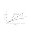
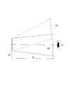
- 1, 2, 3 and 4 show changes in the depth of field when the pupil diameter changes from 4 mm to 0.5 mm.
- the diameter of the human pupil when light is normal is about 3 mm. And when it gets dark, it expands to 5 to 7 mm.
- FIG. 1 shows the depth of field when the pupil diameter is 4 mm.
- FIG. 2 shows the case where the pupil diameter is 2 mm.
- the focus is in the range of 1.2 m to 4 m.
- the focus is in the range of 0.7 m to 1.5 m.
- FIG. 3 shows the depth of field when the pupil diameter is reduced to 1 mm.
- the focus is on from 0.5 m to infinity ( ⁇ ).
- FIG. 4 shows the depth of field when the pupil diameter is reduced to 0.5 mm. It indicates that the camera is in focus from 0.2 m to infinity ( ⁇ ⁇ ) regardless of where the camera is focused at 0.2 m or more.
- ⁇ ⁇ the depth of field
- the angular resolution ⁇ of the eye is determined by the following equation (1).
- ⁇ ⁇ / ⁇ (1)
- the pupil diameter is ⁇
- the wavelength is ⁇ .
- the resolving power (diffraction limit) with a pupil diameter of 2 mm approximately corresponds to a visual acuity of 1.0 (the wavelength was set to 0.55 ⁇ m).
- the pupil is narrowed to 1 mm, the eyesight drops to 0.5.
- the visual acuity decreases to about 0.25.
- the resolution at 300 mm is reduced to about 0.33 mm. If it is this degree, the character of about 3 mm can be seen somehow.
- the visual acuity decreases to 0.1, and the resolution at 300 mm becomes 0.9 mm. Therefore, the lower limit is to narrow the pupil diameter to about 0.5 mm.
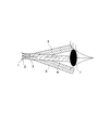
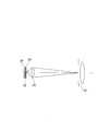
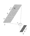
- FIG. 5 shows the basic concept of the display method according to the present embodiment and the basic concept of the display device.
- the image is composed of a plurality of pixels.
- a pixel 1 in FIG. 5 indicates one of a plurality of pixels constituting an image. Since the pixel 1 has a finite area, a plurality of luminous fluxes are emitted from a plurality of light emission points present in this area.
- FIG. 5 shows that the light beam 5 is emitted from the light emission point 2 and the light beams 4 and 6 are emitted from other light emission points.
- the luminous fluxes 4, 5, 6 are incident on the microlens 3. Then, the light beam 4 is projected by the microlens 3 onto the pupil of the observer.
- FIG. 5 shows the basic concept of the display method according to the present embodiment and the basic concept of the display device.
- the image is composed of a plurality of pixels.
- a pixel 1 in FIG. 5 indicates one of a plurality of pixels constituting an image. Since the
- the diameter of the microlens 3 is set to be smaller than the pupil diameter. Accordingly, the light fluxes 4, 5, 6 have a diameter (diameter) limited by the diameter of the microlens 3.
- “projecting to the pupil” is a concept including the equivalent of projecting to infinity ( ⁇ ).
- the light emission point is a light emission point itself.
- a light transmission point limited by a mask having a plurality of openings corresponds to a light emission point.
- the luminous fluxes 4, 5 and 6 from the pixel 1 are directed in the direction of the pupil 7 of the observer.
- the light flux 4 of the plurality of light fluxes enters the pupil 7. Therefore, the depth of field is determined by the light beam 4 having a diameter smaller than the pupil diameter.
- a part of the light of the light flux 5 enters the pupil 7.
- the amount of light is small, so the effect of reducing the depth of field is small. Therefore, it does not matter that part of the light flux 5 enters the pupil.
- at least one limited luminous flux needs to be incident on the pupil.
- the depth of field is made shallow. For this reason, it is preferable that the number of incident light beams is at most four.
- the breakdown of the four luminous fluxes is that there is one luminous flux (corresponding to luminous flux 4) on which the total light quantity of luminous flux is incident, and a luminous flux (corresponding to luminous flux 5) in which part of the luminous flux slightly enters the pupil.
- luminous flux corresponding to luminous flux 4
- luminous flux corresponding to luminous flux 5
- the total amount of light from the luminous flux incident thereon contributes to the brightness of the image and deepens the depth of field.
- the luminous flux which a part of the luminous flux enters is small in light quantity, the effect of reducing the depth of field is small. However, this luminous flux contributes to the brightness of the image, though to some extent.
- the number of light beams is four.
- about four light beams may be incident on the pupil 7.
- the light emission point is not necessarily a point but a finite shape.
- the intensity distribution in the cross section of the light flux (the plane perpendicular to the center of the light flux) is uniform, the boundary of the light flux is clear.
- the intensity distribution may not be uniform. That is, it is possible to use a luminous flux whose boundary of the luminous flux is not always clear.
- the light intensity distribution of the light flux can be a Gaussian distribution like a laser.
- the luminous flux diameter in the case of the Gaussian distribution can be equivalently regarded as a full width at half maximum. Also, even in the case of a Gaussian distribution (in the case of a distribution similar to a Gaussian distribution), the full width at half maximum (the diameter at which the intensity is half, the average size in the case of a finite shape) may be used as the diameter of the light flux .
- each pixel 1 is projected as a light flux onto the pupil 7 of the observer via the microlens 3. Then, at least one of the plurality of luminous fluxes (for example, luminous flux 4) is made incident on the pupil 7 of the eye of the observer to equivalently narrow the pupil and enlarge the depth of field.
- luminous fluxes for example, luminous flux 4
- the diameter of the light beam incident on the pupil 7 of the observer is preferably 2 mm or less.
- a projection light flux group with a diameter of 1 mm is formed on the pupil 7 side.
- a light emission point with a diameter of about 1 ⁇ m is provided.
- the projection magnification of the microlens 3 is 1000 times.
- the light emission points are arranged at a pitch of approximately 2 ⁇ m. How to arrange, such as close-packing, is selected as appropriate.
- the size of the pixel 1 is 100 ⁇ m ⁇ 100 ⁇ m
- the projected area is 100 mm ⁇ 100 mm.
- the information displayed on the display device can be viewed within that range.
- the focal length of the microlens 3 is about 0.3 mm.
- the observer's eyes may be positioned between the adjacent luminous fluxes. In this case, the light flux may not enter the pupil. Therefore, it is desirable to set the distance between one certain luminous flux and the luminous flux adjacent to this luminous flux to be equal to or less than the pupil diameter. Assuming that the normal pupil diameter is 3 mm, the distance between light beams is preferably 3 mm or less. In addition, in order to set the distance between light beams to 3 mm or less at 300 mm, the angular distance between light beams needs to be 0.58 degrees or less. The angular spacing is the angle between the closest rays of light.
- one of the plurality of light beams can be reliably made to enter the pupil. Therefore, the problem that the image can not be observed does not occur depending on the position of the eye of the observer with respect to the display device. That is, if the position of the eye of the observer is substantially directly facing the display device, the image can be observed with certainty.
- the distance to the observer is considered to be 300 mm so that the distance of about 300 mm is easy to see. For this reason, it is preferable to project the image of the light emission point 2 300 mm ahead.
- a distance of about 200 mm may be considered.
- the focal length of the micro lens since the focal length of the micro lens is small, it is almost equivalent to projecting the light emission point 2 at infinity.
- the size of the light emission point 2 is preferably set to about 2 mm or 2 mm or less when projected.
- the size of each of the microlenses 3 corresponds to the size of the pixel 1.
- the size of the microlens 3 is preferably 500 ⁇ m or less.
- the resolution when a person with an eyesight of 1.0 sees an object that is 300 mm far is about 0.1 mm.
- the size (diameter or length of one side) of the microlens 3 is preferably about half of that, that is, about 50 ⁇ m.
- the divergence angle ⁇ ⁇ ⁇ due to diffraction is expressed by the following equation (2).
- ⁇ ⁇ / D (2)
- the wavelength is ⁇
- the size of the aperture is D.
- the size of the microlens 3 is preferably 50 ⁇ m or more.
- the size of the micro lens for keeping the size of the light flux at 1 mm on the pupil 7 is 165 ⁇ m when the observation distance is 300 mm. From the above, it is desirable that the size of the microlens is 50 to 500 ⁇ m.
- the display device When the display device is an electronic device, pixels are present in these devices.
- the electronic device refers to, for example, a liquid crystal panel, a plasma panel, electronic paper (such as one in which micro particles are inverted by electrophoresis), and the like.
- an arbitrary minute range can be regarded as a pixel. This certain range is also referred to as a pixel in the present invention. Therefore, the present invention can be applied to photographic prints without pixels, and the same display can be performed.
- the structure of the display device itself such as a liquid crystal panel or a plasma panel constituting the pixel 1 is omitted. Also in the following drawings, a structure for actually displaying information (ON, OFF, gradation, etc.) on pixels is omitted.
- FIGS. 6A and 6B show arrangement examples of the light emission points 9a and 9b, respectively. It is an example of the light emission point in the case of a self-luminous display device. This corresponds to the mask configuration in the case of the non-self light emitting display device.
- the masks 8a and 8b are respectively provided with openings 9a and 9b for limiting the light flux incident on the pupil.
- the light emitting points or openings 9a, 9b are provided in alignment.
- the invention is not limited to this, and may be randomly arranged.
- the shape does not have to be circular.
- the light emitting points or the openings 9a and 9b are distributed such that one or more and four or less light beams limited to the pupil 7 of the viewer are incident.
- the diameter of the light flux be approximately 1 mm when passing through the pupil 7. In this way, one of the plurality of light beams can be reliably made to enter the pupil. Therefore, the problem that the image can not be observed does not occur depending on the position of the eye of the observer with respect to the display device. That is, if the position of the eye of the observer is substantially directly facing the display device, the image can be observed with certainty.
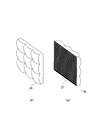
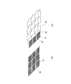
- FIG. 7 shows details of the pixel configuration. For simplicity, 3 ⁇ 3 pixels are shown. In the case of a self-luminous display such as a plasma panel, the pixels 10, the mask 11, and the microlens array 12 are in this order. In FIG. 7, the microlenses of the microlens array 12 correspond to each pixel. Not limited to this, a plurality of microlenses may correspond to one pixel.
- the mask 11 is not necessary in the case of a display device such as an organic EL in which the shape of the light emitting point can be set arbitrarily.
- the pixel 10 may use a liquid crystal display panel. Although a space and a gap are illustrated between the pixel 10, the mask 11, and the microlens array 12, it is not always necessary.
- the pixel 10, the mask 11, and the microlens array 12 may be integrally adhered.
- FIG. 8 shows an example of another pixel configuration.
- a non self-luminous display such as a liquid crystal panel (usually called "LCD") and a display requiring a light source on the back
- the light source 13 may be a light guide plate.
- the pixel 15 is preferably a pixel of a liquid crystal panel.
- blocked by the mask can be returned to a light guide plate. Thereby, light can be used effectively.
- the surface on the light guide plate side of the mask 14 is preferably a reflective surface. It is illustrated that a space or a gap is provided between the light source 13, the mask 14, the pixels 15, and the microlens array 16, but this is not always necessary. These may be integrally and closely attached.
- FIGS. 7 and 8 although the arrangement of vertical and horizontal matrixes of pixels and corresponding micro lenses is described, the arrangement is not limited thereto. It is desirable to match the pixel arrangement of the display device to be used. Further, in the case of color display using red (R), green (G), blue (B) or the like, it is conceivable to allocate pixels to R, G, B or to switch time division (color sequential).
- FIG. 9 shows a configuration in which the image of the mask is projected onto the pupil of the observer's eye.
- the mask 18 provided in contact with the light guide plate 17 is further in contact with the pixels 19.
- the display element is made up of a plurality of pixels.
- the pixel 19 is a pixel of the liquid crystal panel.
- the surface on the light guide plate 17 side of the mask 18 is a reflective surface.
- the mask 18 and the aperture group formed therein are projected by the microlens 20 to the pupil 21 side of the observer.
- the mask 18 and the microlens 20 may be arranged in order on a normal liquid crystal panel.
- a projection pupil group having a diameter of 1 mm is formed on the pupil 21 side.
- a mask having an aperture group of 1 ⁇ m is provided.
- the projection magnification of the microlens 20 is 1000 times.
- the openings are arranged at a pitch of approximately 2 ⁇ m. How to arrange, such as close-packing, is selected appropriately.
- the projected area is 100 mm ⁇ 100 mm.
- the information displayed on the display device can be viewed within that range. The situation is shown in FIG.
- the information displayed on the display 22 according to the invention can be viewed in focus in the area 23.
- the mask of the adjacent pixel is projected, so that the image can be viewed even in that direction.
- the observer and the display device are separated by a distance dt.
- the focal length of the microlens 20 is about 0.3 mm.
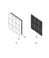
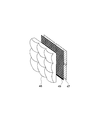
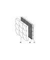
- FIGS. 11A and 11B show a schematic configuration of an optical unit according to the third embodiment. Usually, many micro lenses are provided. Here, 3 ⁇ 3 of them are shown. This is a plate composed of the microlens array 26 and the mask 27.
- FIGS. 11A and 11B are views of the optical unit as viewed from the front and the back, respectively.
- the configuration requirements of the microlens array 26 and the mask 27 are the same as in the previous embodiment. That is, a plurality of mask openings exist in one microlens.
- the microlens projects the image of the mask 27 having the aperture forward. Then, the focal length of the micro lens, the distance between the micro lens and the mask, and the size and density of the mask are set such that one or more apertures are projected onto the observer's pupil. It is preferable that the projection distance of the microlenses of the mask 27 be adjusted to the distance observed by the observer.
- the display device includes electronic devices such as liquid crystal panels, and paper media such as photographic prints and newspapers.
- the mask 27 is preferably provided directly on the planar side of the microlens array 26.
- the microlens array 26 can also be made of a flexible material, for example, a soft material such as plastic. Thereby, it is applicable to a flexible display.
- the projection magnification of the microlens is 500 times. Assuming that the distance to the observer is 300 mm, the focal length of the microlens is 0.6 mm.
- the mask 27 is placed at the focal position of the microlens 26. When placed at the focal position, the projection is infinite, but since the focal length of the lens is small, it is equivalent to projection 300 mm ahead.
- the size (length of one side) of the microlens and the size of the pixel are 150 ⁇ m.
- the image can be observed in the range of 75 mm square. Assuming that the distance between the openings closest to each other is 6 ⁇ m, the distance is 3 mm at the position of the observer. If you move the pupil 3 mm, you will see the light flux generated by the next aperture. At this time, the angle formed by the luminous flux is about 0.57 degrees.
- the projection magnification of the microlens is 300 times. Assuming that the distance to the observer is 300 mm, the focal length of the microlens is 1 mm.
- the mask 27 is placed at the focal position of the microlens. When placed at the focal position, the projection is infinite, but since the focal length of the lens is small, it is equivalent to projection 300 mm ahead.
- the size (length of one side) of the microlens and the size of the pixel are 200 ⁇ m, an image can be observed in a 60 mm square range. Assuming that the distance between the openings closest to each other is 10 ⁇ m, the distance is 3 mm at the position of the observer. If you move the pupil 3 mm, you will see the light flux generated by the next aperture. At this time, the angle formed by the luminous flux is about 0.57 degrees.
- the projection magnification of the microlens is 200 times. Assuming that the distance to the observer is 300 mm, the focal length of the microlens is 1.5 mm.
- the mask 27 is placed at the focal position of the microlens. When placed at the focal position, the projection is infinite, but since the focal length of the lens is small, it is equivalent to projection 300 mm ahead.
- the size (length of one side) of the microlens and the size of the pixel are 200 ⁇ m, an image can be observed in a 40 mm square range. Assuming that the distance between the openings closest to each other is 15 ⁇ m, the distance is 3 mm at the position of the observer. If you move the pupil 3 mm, you will see the light flux generated by the next aperture. At this time, the angle formed by the luminous flux is about 0.57 degrees.
- the projection magnification of the microlens is 100 times. Assuming that the distance to the observer is 300 mm, the focal length of the microlens is 2.97 mm.
- the mask 27 is placed at the focal position of the microlens. When placed at the focal position, the projection is infinite, but since the focal length of the lens is small, the projection is approximately equivalent even when projecting 300 mm ahead.
- the size (length of one side) of the microlens and the size of the pixel are 500 ⁇ m, an image can be observed within a 50 mm square range. Assuming that the distance between the openings closest to each other is 30 ⁇ m, the distance is 3 mm at the position of the observer. If you move the pupil 3 mm, you will see the light flux generated by the next aperture. At this time, the angle formed by the luminous flux is about 0.57 degrees.
- the aperture of the mask 27 is 20 ⁇ m and a light beam of 2 mm is incident on the pupil of the observer, the projection magnification of the microlens is 100 times. Assuming that the distance to the observer is 300 mm, the focal length of the microlens is 2.97 mm. When the size (length of one side) of the micro lens and the size of the pixel are 250 ⁇ m, an image can be observed in a range of 25 mm square.
- FIG. 12 (a) and 12 (b) show a schematic configuration of a display device according to a fourth embodiment. Usually, many micro lenses are formed. Here, 3 ⁇ 3 of them are shown for simplicity.
- FIG. 12 (b) shows a pixel 28 made of an organic EL device.
- the organic EL is a self light emitting element, and a plurality of light emitting points are formed in a pixel.
- a large number of highly directional limited luminous fluxes are generated by the light emitting point and the microlenses of the microlens array 29 shown in FIG. 12A. It is incident on the observer's pupil like the light flux shown in FIG. 5, and the observer's pupil is equivalently narrowed to enlarge the depth of field.
- the depth of field of the observer can be increased with a simple configuration without using a mask.
- it may be limited by a mask.
- the projection magnification of the microlens is 1000 times when a light beam of 2 mm is to be incident on the pupil of the observer.
- the focal length of the microlens is 0.25 mm.
- the size of the microlens (length of one side) and the size of the pixel are 100 ⁇ m, an image can be observed within a 100 mm square range.
- the projection magnification of the microlens is 100 times when a light flux of 1 mm is to be incident on the pupil of the observer.
- the focal length of the microlens is 3 mm.
- FIGS. 13A and 13B show a schematic configuration of a display device according to a fifth embodiment and a method of manufacturing the same.
- the display device includes, as a display device, a photograph, a printed matter, etc. in addition to the liquid crystal and the organic EL as described above.
- the display device is a printed matter.
- the value (density, color, etc.) of the information is displayed on a medium such as paper by printing etc with fine dots 31 in the range 30 corresponding to each pixel.
- a thin lens material 32 is applied thereon.
- the microlens array 33 is formed by a technique such as nanoimprinting.
- the microlens array 33 may be formed first and then attached to the pixel.
- the microlens may be formed when the transparent material is transferred onto the medium on which the information is displayed.
- the fine dots 31 correspond to light emission points, and reflect light from the surface. Alternatively, it transmits light from the back.
- the actions and effects are the same as in the previous example.
- a deep print with a deep depth of field can be provided at the same cost as printing. In other words, it is possible to provide a printed matter that is easy for people with presbyopia and myopia to see.
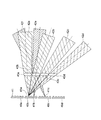
- FIG. 14 shows the basic concept of the display method according to the present embodiment and the basic concept of the display device.
- the image is composed of a plurality of pixels.
- FIG. 5 described above the basic concept is schematically described.
- FIG. 5 in order to explain the concept in an easy-to-understand manner, it is assumed that the diameter of the micro-lens limits the light flux, but in FIG.
- a pixel 61 in FIG. 14 indicates one of a plurality of pixels forming an image. Since the pixel 61 has a finite area, a plurality of luminous fluxes are emitted from a plurality of light emission points present in this area.
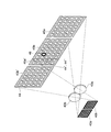
- FIG. 14 shows how the light emitted from the light emission point 62 becomes the light flux 65 by the lens 63 of the microlens array. The light emitted from the other light emission points is also shown by the lens 63 to be the light fluxes 64 and 66, respectively. As described above, the light emitted from the light emission point becomes the light flux 64 by the lens 63 and is incident on the pupil 67 of the observer.
- the diameter of the microlens array is very small compared to the pupil diameter. Further, the microlens array and the pixel (light emission point) are close to each other. Therefore, this is equivalent to the light emission point being imaged on the observer's pupil 67 by the lens 63. Further, since the focal length of the lens 63 is very small compared to the distance to the observer, hereinafter, “projecting on the pupil” means projecting the light emitted from the light emission point to infinity ()) It is a concept that includes being equal to
- the light emission point is a light emission point itself.
- a light transmission point limited by a mask having a plurality of openings corresponds to a light emission point.
- the light fluxes 64, 65, 66 from the pixel 61 are directed in the direction of the pupil 67 of the observer. That is, the light emission point of the pixel 61 is imaged by the lens 63 at the position (the distance from the lens) of the pupil 67 of the observer. Then, in this example, only the light flux 64 of the plurality of light fluxes is incident on the pupil 67. Therefore, the depth of field is determined by the light beam 64 having a diameter smaller than the pupil diameter.
- part of the light of the light flux 65 is incident on the pupil 67.
- the amount of light is small, so the effect of reducing the depth of field is small. Therefore, it does not matter that part of the light flux 65 enters the pupil.
- at least one limited luminous flux needs to be incident on the pupil.
- the depth of field is made shallow. For this reason, it is preferable that the number of incident light beams is at most four.
- the breakdown of the four luminous fluxes is that there is one luminous flux (corresponding to luminous flux 64) for which the total light quantity of luminous flux is incident, and luminous flux (corresponding to luminous flux 65) for which part of the luminous flux slightly enters the pupil. There are three.
- the total amount of light from the luminous flux incident thereon contributes to the brightness of the image and deepens the depth of field.
- the luminous flux which a part of the luminous flux enters is small in light quantity, the effect of reducing the depth of field is small. Therefore, in order to keep the depth of field deep, it is preferable that the number of luminous fluxes is four or less.
- about four light beams may be incident on the pupil 67.
- the light emission point is not necessarily a point but a finite shape.
- the boundary of the light flux is clear.
- luminous flux may be used.
- the present invention is not limited to this, and the intensity distribution may not be uniform. That is, it is possible to use a luminous flux whose boundary of the luminous flux is not always clear.
- the light intensity distribution of the light flux can be a Gaussian distribution like a laser. Even in the case of the Gaussian distribution, since the central intensity is strong, it has the same effect as a normal luminous flux.
- the luminous flux diameter in the case of the Gaussian distribution can be equivalently regarded as a full width at half maximum. Also, even in the case of a Gaussian distribution (in the case of a distribution similar to a Gaussian distribution), the full width at half maximum (the diameter at which the intensity is half, the average size in the case of a finite shape) may be used as the diameter of the light flux. .
- the light emitted from each pixel 61 is projected as a light flux onto the pupil 67 of the observer via the lens 63 of the microlens array. Then, by causing at least one of the plurality of light beams (for example, the light beam 64) to be incident on the pupil 67 of the eye of the observer, the pupil is equivalently narrowed to expand the depth of field.
- the plurality of light beams for example, the light beam 64
- the diameter of the light beam incident on the pupil 67 of the observer is preferably 2 mm or less.
- a projection light flux group with a diameter of 1 mm is formed on the pupil 67 side.
- a light emission point of about 1 ⁇ m in diameter is provided.
- the projection magnification of the lens 3 is said to be 1000 times.
- the light emission points are arranged at a pitch of approximately 2 ⁇ m. How to arrange, such as close-packing, is selected as appropriate. Assuming that the observation distance is 300 mm, the focal length of the lens 3 is about 0.3 mm.
- the distance between the light emission points be greater than twice the size of the light emission points.
- the distance between the light emission points is the distance between the centers of the light emission points.
- the observer's eyes may be positioned between the adjacent luminous fluxes. In this case, the light flux may not enter the pupil. Therefore, it is desirable to set the distance between one certain luminous flux and the luminous flux adjacent to this luminous flux to be equal to or less than the pupil diameter. Assuming that the normal pupil diameter is 3 mm, the distance between light beams is preferably 3 mm or less. In addition, in order to set the distance between light beams to 3 mm or less at 300 mm, the angular distance between light beams needs to be 0.58 degrees or less. The angular spacing is the angle between the closest rays of light.
- one of the plurality of light beams can be reliably made incident on the pupil. Therefore, the problem that the image can not be observed does not occur depending on the position of the eye of the observer with respect to the display device. That is, if the position of the eye of the observer is substantially directly facing the display device, the image can be observed with certainty.
- the distance to the observer is considered to be 300 mm so that the distance of about 300 mm is easy to see. For this reason, it is preferable to project the image of the light emission point 62 300 mm ahead.
- the focal length of the lens 63 is small, it is almost equivalent to projecting the light emission point 62 at infinity. Also, the size of the light emission point 62 is preferably set to about 2 mm or 2 mm or less when projected.
- the size of the lens 63 is a factor that determines the resolving power as in the case of the pixel. For this reason, in order to perform high definition display, the size of the lens 63 is preferably 500 ⁇ m or less. Furthermore, the resolution when a person with an eyesight of 1.0 sees an object that is 300 mm far is about 0.1 mm. For this reason, the size (diameter or length of one side) of the lens 63 is preferably about half of that, that is, about 50 ⁇ m.
- the divergence angle ⁇ ⁇ ⁇ due to diffraction is expressed by the following equation (2).
- ⁇ ⁇ / D (2)
- the wavelength is ⁇
- the size of the aperture is D.
- the size of the lens 63 is preferably 50 ⁇ m or more.
- the size of the lens for keeping the size of the light flux at 1 mm on the pupil 67 is 165 ⁇ m when the observation distance is 300 mm. From the above, it is desirable that the size of the lens be 50 to 500 ⁇ m.
- the display device When the display device is an electronic device, pixels are present in these devices.
- the electronic device refers to, for example, a liquid crystal panel, a plasma panel, electronic paper (such as one in which micro particles are inverted by electrophoresis), and the like.
- an arbitrary minute range can be regarded as a pixel. This certain range is also referred to as a pixel in the present invention. Therefore, the present invention can be applied to photographic prints without pixels, and the same display can be performed.
- FIG. 14 the structure of the display device itself such as a liquid crystal panel or a plasma panel constituting the pixel 61 is omitted. Also in the following drawings, a structure for actually displaying information (ON, OFF, gradation, etc.) on pixels is omitted.
- FIGS. 6A and 6B show arrangement examples of the light emission points 9a and 9b, respectively. It is an example of the light emission point in the case of a self-luminous display device. This corresponds to the mask configuration in the case of the non-self light emitting display device.
- the masks 8a and 8b are respectively provided with openings 9a and 9b for limiting the light flux incident on the pupil.
- the light emitting points or openings 9a, 9b are provided in alignment.
- the invention is not limited to this, and may be randomly arranged.
- the shape does not have to be circular.
- the light emitting points or the openings 9a and 9b are distributed such that one or more and four or less light beams limited to the observer's pupil 67 are incident.
- the diameter of the light flux be approximately 1 mm when passing through the pupil 67. In this way, 61 of the plurality of light beams can be reliably made incident on the pupil. Therefore, the problem that the image can not be observed does not occur depending on the position of the eye of the observer with respect to the display device. That is, if the position of the eye of the observer is substantially directly facing the display device, the image can be observed with certainty.
- FIG. 14 is described by representing one pixel and one lens for the sake of simplicity, it is not always necessary to make the pixel and the lens correspond one to one.
- FIG. 15 shows a configuration in which the pixel and the lens do not correspond one to one.
- a display device having a plurality of pixels 40a, 40b, 40c, 40d, a plurality of light emitting points 41 formed in each pixel and a plurality of light beams 42a, 42b, 42c, 42d, 42e emitted from the light emitting points 41a.
- 42f show lenses 43a, 43b, 43c, 42d of the microlens array.
- a display device used for normal FPD such as liquid crystal and organic EL, can be used.
- the necessary luminous flux as shown in FIG. 15 can be formed only with the configuration shown here. Although only a plurality of light emission points 41a and the like formed in the pixels 40a to 40d are drawn, it goes without saying that a large number of the light emission points 41a and the like are provided in the pixels 40a to 40d.
- each of the pixels 40a to 40d is an arrangement of images to be displayed. Also as to the luminous fluxes 42a to 42f, only representative ones are displayed. In practice, the light from all the light emission points of all the drawn pixels forms a luminous flux respectively by all the lenses.
- the light emitted from the light emission point 41a of the pixel 40b generally diverges and spreads.
- the diffused light is formed into light fluxes 42a, 42b, 42c and 42d by lenses 43a, 43b, 43c and 43d, respectively.
- light diverging from another light emission point 41b of the pixel 40b is similarly formed into a light flux by the lenses 43a, 43b, 43c and 43d.
- only the luminous flux 42e formed by the lens 43b is shown.
- light diverging from the light emission point 41c of the other pixel 40c is also formed into a light flux by the lenses 43a, 43b, 43c, and 43d.
- the lenses of the microlens array form light that emits light from all light emission points of all pixels into a light flux.
- the formation of a light flux by one lens will be described in more detail with reference to FIG.
- the pixels 40a, 40b, and 40c are projected by the lens 43 into projected images 45a, 45b, and 45c.
- the light emission points 41 respectively provided in the pixels 40a, 40b, and 40c are also projected by the lens 43 to form a cross section 44 of a light flux shape. It can be seen how one pixel projects each pixel and each light exit point. When the pupil 46 of the observer's eye is in the position shown, the observer can observe the pixel 40a.
- the luminous flux incident on the pupil is smaller than the pupil diameter of the observer's eye. For this reason, as described in the above-described embodiment, the depth of field is deep. As a result, even a person who is not in focus at the position of the display device can see the in-focus display.
- microlens array The effect of the microlens array will be described with reference to FIG. For simplicity, only two pixels 40a and 40b are shown. The lenses of the microlens array also show only two lenses 43a and 43b.
- the pixels 40 a and 40 b are projected toward the viewer by the lens 43 a to form projected images 45 a and 45 b of the pixels.
- the pixels 40a and 40b are projected toward the viewer by the lens 43b to form projected images 45a 'and 45b' of the pixels.
- the pixels and the lenses of the microlens array do not correspond one to one. That is, the distance from the center of the pixel 40a to the center of the pixel 40b is different from the distance from the center of the lens 43 to the lens 43b. Therefore, the projected images 45a 'and 45b are partially overlapped.
- the light emission point provided in each pixel forms a shape 44 as a light flux.
- the pixels 40a, 40b can be observed. That is, the pixel 40b can be observed by the light flux 44 'of the pixel image 45b projected by the lens 43a. Further, the pixel 40a can be observed by the light flux 44 "of the pixel image 45a projected by the lens 43b.
- the light flux 44 'and the light flux 44" almost overlap in the figure.
- the light flux of the pixels is projected onto the pupil from each lens of the microlens array, so that an image can be viewed.
- the pixels and the lenses of the microlens array do not correspond one to one, but may not necessarily correspond to one another.
- the projected images 45a 'and 45b overlap without deviation in the enlarged projected image, which is equivalent to the pixel coincidence.
- FIG. 18 and 19 show details of the pixel configuration.
- a 3 ⁇ 3 microlens array 48 corresponds to 2 ⁇ 2 pixels 47.
- a 3 ⁇ 3 microlens array 48 corresponds to 4 ⁇ 4 pixels 47.
- the pixels 47, the mask 49 and the microlens array 48 are arranged in this order.
- one light flux from each of the three lenses enters the pupil of the observer.
- the resolution of the present display device is limited by either the number of pixels or the number of microlenses, whichever is smaller. Therefore, it is preferable that the lenses of the microlens array 48 correspond to each pixel (see FIG. 7 of the first embodiment).
- the size of the pixel is also preferably 500 ⁇ m or less.
- two pixels may be provided corresponding to one microlens of the microlens array.
- the display device of the present embodiment is different in that each pixel has a plurality of light emission points, and that the arrangement of pixels is an arrangement of images to be displayed. That is, the right-eye image and the left-eye image are not alternately displayed for each adjacent pixel.
- FIG. 20 and 21 show another example of the pixel configuration.
- a 3 ⁇ 3 microlens array 53 corresponds to 2 ⁇ 2 pixels 52.
- a 3 ⁇ 3 microlens array 53 corresponds to 4 ⁇ 4 pixels 52.
- the light source 50 may be a light guide plate.
- the microlenses of the microlens array 53 have the same size corresponding to each pixel (FIG. 8 of the first embodiment).
- the pixel 52 is preferably a pixel of a liquid crystal panel.
- the surface on the light source (light guide plate) 50 side of the mask 51 as a reflection surface, light blocked by the mask can be returned to the light guide plate. Thereby, light can be used effectively.
- the surface on the light guide plate side of the mask 51 is preferably a reflective surface. Note that although a space and a gap are illustrated between the light source 50, the mask 51, the pixels 52, and the microlens array 53, this is not always necessary. These may be integrally and closely attached.
- FIG. 18 to FIG. 21 although the arrangement of vertical and horizontal matrixes is described for the pixels and the corresponding micro lenses, the arrangement is not limited to this. It is desirable to match the pixel arrangement of the display device to be used. Further, in the case of color display using red (R), green (G), blue (B) or the like, it is conceivable to allocate pixels to R, G, B or to switch time division (color sequential).
- RGB red
- G green
- B blue
- FIG. 22 shows the appearance of a digital camera.
- the digital camera 160 has an imaging lens (not shown) on the entire surface. Further, the main body is provided with a release button 161, a mode button 162, and a display device 163.
- the display device 163 a display device having a pixel configuration provided with the microlens array shown in FIG. 8 and a mask having a light emission point is used. Therefore, even a person with presbyopia can confirm the displayed image without wearing reading glasses. In addition, focus, composition and information can also be confirmed.
- the mode button is a switch for setting shooting conditions such as shooting sensitivity, landscape mode, night view mode, and the like, and also includes a zoom lever (a switch for operating a zoom) not shown. Although only one is shown here, there may be more than one.
- FIG. 23 shows the appearance of a mobile phone.
- the mobile phone 70 includes a call switch, a numeric keypad 72 for character input, and a display device 71.
- the mobile phone is equipped with a display device for acquiring information not only by telephone but also by mail or Internet connection.
- a display device for acquiring information not only by telephone but also by mail or Internet connection.
- people with presbyopia had difficulty in focusing on the display with their naked eyes, and it was hard to see mail letters and Internet information. I had to wear reading glasses to see the display.
- the mobile phone 70 of this embodiment uses, as the display device 71, the microlens array shown in FIG. 7 and an organic EL device of a pixel configuration having a plurality of light emitting points in one pixel.
- the liquid crystal device shown in FIG. 8 may be used as the display device 71.
- the display method according to the present invention the display apparatus using the same, and the optical unit enlarge the focal depth of the eye by making the luminous flux incident on the pupil of the observer smaller than the pupil diameter, and as a result, the depth of field It is possible to magnify and view an in-focus display even if the display position is not in focus.
- the display method, the display device and the optical unit of the present invention even a person with a presbyopia can see an in-focus display without putting on (disengaging) reading glasses. Furthermore, the burden on the eyes of the presbyopia observer can be reduced, and observation can be performed without adding reading glasses or other optical members. Therefore, even a person with a presbyopia can see the monitor screen of a mobile phone, a digital camera, a car navigation system, and a PC in focus without having to disconnect the reading glasses. Furthermore, even people with hyperopia, myopia and astigmatism can see in-focus images (not only pictures but all the information displayed, such as letters) without using glasses.
- the present invention is useful for a display device such as a flat panel display, and an electronic device equipped with such a display device.
- pixels 11 masks 12 microlens arrays 13 light sources 14 masks 15 pixels 16 microlens arrays 17 light guide plate 18 masks 19 pixels 20 microlenses 21 pupils 22 display devices 23 24 ranges 26 microlens arrays 27 masks 28 pixels 29 microlens arrays 30 Pixel 31 dot 32 lens 33 micro lens array 40a, 40b, 40c, 40d pixel 41 light emission point 42a, 42b, 42c, 42d, 42e, light beam 43a, 43b, 43c, 42d lens 45a, 45b, 45c projection image 46 pupil 47 pixels 48 micro lens array 49 mask 50 light source 51 mask 52 pixels 53 micro lens array 61 pixels 62 light emitting point 63 lens 64, 65, 66 light flux 67 pupil 70 mobile phone 71 Display device 72 ten-key 73 camera mode switch 160 digital camera 161 release button 162 mode button 163 display dt distance
Abstract
複数の画素を用いて画像を形成する表示方法であって、複数の画素からの光束を観察者の眼の瞳に投影し、瞳に入射する光束の径は、瞳の径よりも小さいことを特徴とする。 また、表示装置は、複数の画素を有する画像を表示する表示装置において、各画素に対応して複数の光射出点が形成され、各画素に対応するレンズを有するマイクロレンズアレイが設けられたことを特徴とする。 また、電子機器は、その表示装置を搭載することを特徴とする。
Description
本発明は、表示方法、表示装置、光学ユニット、表示装置の製造方法、及びその表示装置を搭載した電子機器に関するものである。
映像や文字を表示する表示装置(ディスプレイ)として、液晶ディスプレイやプラズマディスプレイがある。ここで、これらの表示装置は視度の調節が出来ない。ところで、高齢化社会の進展に伴って老眼(老視)の高齢者が増えている。このような老眼(老視)の高齢者でも、表示装置を容易に見るようにできることが望ましい。このため、視度調節が可能な表示装置、特にフラットパネルディスプレイ(適宜、「FPD」という)が望まれている。
特に、携帯電話の普及やデジタルカメラの普及により、屋外でFPDによる表示を見る機会が増えている。携帯電話やデジタルカメラのFPDを見る時、その都度、老眼鏡を掛けるのは非常に煩わしい。
また、デジタル一眼レフカメラには、ライブビューモニターとしてFPDが用いられている。デジタル一眼レフカメラにおいて、遠方の被写体を見つつ、ライブビューモニターを見るために、その都度、老眼鏡を掛けたり外したりするのは、実際的ではない。
また、カーナビゲーションシステムのモニターを見るときは、観察者は運転中である。このため、老眼鏡を掛け外しするのは危険であり、事実上不可能である。さらに、この他にも、パソコン(PC)の液晶画面を観察するときも、観察者が、その都度、老眼鏡を掛けるのは煩わしい。そこで、老眼鏡を掛け外しすることなく、モニターを見ることができる電子機器が望まれている。
すなわち、従来、老眼鏡を掛けなくても焦点の合った画像を見ることの出来るFPDは存在していなかった。また、そのような電子機器は存在していなかった。老眼鏡等、メガネの掛け外しが必要であった。最近ではこのような問題は指摘されつつある。例えば、特許文献1には、エッジ強調をした補正画像を表示する方法が提案されている。また、特許文献2にはテプリッツ行列の逆行列で生成した事前補正画像を用いる方法が提案されている。更に特許文献3にはルーペを用いる方法が提案されている。
特許文献1によるエッジ強調の手法では、表示情報を多少見易くはするものの、デフォーカス像を回復することは不可能である。像がボケる原因はデフォーカスによるものであるが、特許文献1における補正はデフォーカスの情報を用いた補正ではないので、デフォーカス像を回復できないのは当然である。
また、特許文献2では、眼の焦点調節不足による点広がり関数からなるテプリッツ行列を用いて画像を補正している。補正画像データに複素数は生じないものの、その結果、特許文献1と同じエッジ強調程度の補正に留まり、実際の効果は少なく実用には至っていない。
更に、特許文献3では、フレネルレンズをデジタルカメラのモニターであるFPDの手前に取り付け、ルーペのようにFPDを覗く構成例が示されている。しかしながら、老眼の補正をする為には、フレネルレンズをFPDから数cm程度の距離まではなす必要があり、実用的ではない。
本発明は、上記に鑑みてなされたものであって、焦点が容易に合う表示方法とそれを利用した表示装置、光学ユニット、表示装置の製造方法、及びその表示装置を搭載した電子機器を提供することを目的とする。
上述した課題を解決し、目的を達成するために、第1の側面に従う本発明は、
複数の画素を用いて画像を形成する表示方法であって、
複数の画素からの光束を観察者の眼の瞳に投影し、
瞳に入射する光束の径は、瞳の径よりも小さいことを特徴とする表示方法を提供できる。
複数の画素を用いて画像を形成する表示方法であって、
複数の画素からの光束を観察者の眼の瞳に投影し、
瞳に入射する光束の径は、瞳の径よりも小さいことを特徴とする表示方法を提供できる。
また、本発明の好ましい態様によれば、一つの画素から発する光を、互いに分離した複数の光束として投射し、
複数の光束のうちの少なくとも一つの光束を、観察者の眼の瞳に入射させることが望ましい。
複数の光束のうちの少なくとも一つの光束を、観察者の眼の瞳に入射させることが望ましい。
また、本発明の好ましい態様によれば、一つの画素に複数の光射出点を設けることにより、互いに分離した複数の光束を形成することが望ましい。
また、本発明の好ましい態様によれば、画素から発する光を、画素に対応するレンズによって光束に形成することが望ましい。
また、本発明の好ましい態様によれば、複数の光束のうち、一つ以上で、且つ四つ以下の光束が、観察者の瞳に入射するよう光射出点を配置していることが望ましい。
また、本発明の好ましい態様によれば、観察者の瞳に入射する光束の径は0.5mmから2mmまでであることが望ましい。
また、本発明の好ましい態様によれば、レンズによって光射出点を、レンズの位置よりも200mm以遠に投影することが望ましい。
また、本発明の好ましい態様によれば、互いに分離した複数の光束のうち、最も近接する光束どうしが相互に成す角は0.58度以下であることが望ましい。
また、本発明の好ましい態様によれば、該複数の光射出点は、複数の開口を有するマスクを用いて形成することが望ましい。
また、第2の側面にしたがう本発明によれば、複数の画素を有する画像を表示する表示装置において、
各画素に対応して複数の光射出点が形成され、
各画素に対応するレンズを有するマイクロレンズアレイが設けられたことを特徴とする表示装置を提供できる。
各画素に対応して複数の光射出点が形成され、
各画素に対応するレンズを有するマイクロレンズアレイが設けられたことを特徴とする表示装置を提供できる。
また、他の側面にしたがう本発明によれば、複数の画素を有する画像を表示する表示装置において、
各画素に複数の光射出点が形成され、
光射出点から発する光を複数の光束に形成するレンズを有するマイクロレンズアレイが設けられたことを特徴とする表示装置を提供できる。
各画素に複数の光射出点が形成され、
光射出点から発する光を複数の光束に形成するレンズを有するマイクロレンズアレイが設けられたことを特徴とする表示装置を提供できる。
また、本発明の好ましい態様によれば、複数の画素配列が、表示される画像の配列であることが望ましい。
また、本発明の好ましい態様によれば、複数の光射出点から発する光を、画素に対応するレンズによって光束を形成することが望ましい。
また、本発明の好ましい態様によれば、光束を、表示装置を使用する観察者の瞳に入射させることにより像を生じせしめることが望ましい。
また、本発明の好ましい態様によれば、複数の光射出点からの光束の径は、観察者の眼の瞳の径よりも小さいことが望ましい。
また、本発明の好ましい態様によれば、複数の光束のうち、一つ以上で、且つ四つ以下の光束が、観察者の瞳に入射するよう光射出点を配置していることが望ましい。
また、本発明の好ましい態様によれば、光射出点の間隔は、光射出点の大きさの2倍より大きいことが望ましい。
また、本発明の好ましい態様によれば、表示装置を使用する観察者の瞳に入射する光束の径は0.5mmから2mmまでであることが望ましい。
また、本発明の好ましい態様によれば、マイクロレンズアレイによって、光射出点を、表示装置を使用する観察者の眼の瞳の位置に投影することが望ましい。
また、本発明の好ましい態様によれば、レンズによって光射出点を、レンズの位置よりも200mm以遠に投影することが望ましい。
また、本発明の好ましい態様によれば、マイクロレンズアレイが有する各レンズの大きさは50~500μmであることが望ましい。
また、本発明の好ましい態様によれば、画素の大きさが500μm以下であることが望ましい。
また、本発明の好ましい態様によれば、複数の光射出点は開口で構成されていることが望ましい。
また、本発明の好ましい態様によれば、開口はマスク上に設けられていることが望ましい。
また、本発明の好ましい態様によれば、マスクは、画素の位置よりもマイクロレンズ側の位置に設けられていることが望ましい。
また、本発明の好ましい態様によれば、画素は液晶で構成されていることが望ましい。
また、本発明の好ましい態様によれば、マスクは、液晶の位置よりも導光板側の位置に配置されていることが望ましい。
また、本発明の好ましい態様によれば、マスクの導光板側の面は反射面で構成されていることが望ましい。
また、本発明の好ましい態様によれば、画素は有機ELデバイスで構成されていることが望ましい。
また、第3の側面にしたがう本発明によれば、複数のマイクロレンズからなるマイクロレンズアレイと、
レンズの一つずつに応じて複数の開口を有するマスクと、を有する光学ユニットを提供できる。
レンズの一つずつに応じて複数の開口を有するマスクと、を有する光学ユニットを提供できる。
また、本発明の好ましい態様によれば、マスクはマイクロレンズアレイに一体的に形成されていることが望ましい。
また、本発明の好ましい態様によれば、レンズによってマスクの像をレンズよりも200mm以遠に投影することが望ましい。
また、本発明の好ましい態様によれば、レンズの大きさは50~500μmであることが望ましい。
また、本発明の好ましい態様によれば、マイクロレンズアレイは、柔軟性を有する材料で成ることが望ましい。
また、第4の側面にしたがう本発明によれば、複数の画素を有する画像を表示する表示装置の製造方法であって、
画素に対応する範囲に複数の光射出点を設ける工程と、
複数の射出点の近傍にマイクロレンズアレイを形成する工程とを有する表示装置の製造方法を提供できる。
画素に対応する範囲に複数の光射出点を設ける工程と、
複数の射出点の近傍にマイクロレンズアレイを形成する工程とを有する表示装置の製造方法を提供できる。
また、本発明の好ましい態様によれば、複数の光射出点を画素上に印刷で形成することが望ましい。
また、本発明の好ましい態様によれば、マイクロレンズアレイが有するレンズを各画素に対応して配置する工程を有することが望ましい。
また、本発明の好ましい態様によれば、マイクロレンズアレイはナノインプリントによって形成されることが望ましい。
また、本発明の好ましい態様によれば、マイクロレンズアレイを画素に接合する工程を有することが望ましい。
また、本発明の好ましい態様によれば、複数の光射出点からの光束の径は、表示装置を使用する観察者の眼の瞳の径よりも小さいことが望ましい。
また、本発明の好ましい態様によれば、複数の光射出点の光束のうち、一つ以上で、且つ四つ以下の光束が、観察者の瞳に入射するよう光射出点を配置していることが望ましい。
また、本発明の好ましい態様によれば、表示装置を使用する観察者の瞳に入射する光束の径は0.5mmから2mmまでであることが望ましい。
また、本発明の好ましい態様によれば、レンズによって光射出点を、レンズの位置よりも200mm以遠に投影することが望ましい。
また、本発明の好ましい態様によれば、レンズの大きさが50~500μmであることが望ましい。
また、他の側面にしたがう本発明によれば、上述の表示装置を備えることを特徴とする電子機器を提供できる。
また、他の側面にしたがう本発明によれば、上述の表示装置を備えることを特徴とする携帯用電子機器を提供できる。
また、他の側面にしたがう本発明によれば、上述の表示装置を備えることを特徴とする携帯電話を提供できる。
また、本発明の好ましい態様によれば、メール機能を備えることが望ましい。
また、本発明の好ましい態様によれば、カメラ機能を備えることが望ましい。
また、他の側面にしたがう本発明によれば、上述の表示装置を備えることを特徴とする撮像装置を提供できる。
また、本発明の好ましい態様によれば、撮影条件を設定するスイッチが設けられることが望ましい。
本発明は、焦点が容易に合う表示方法とそれを利用した表示装置、光学ユニット、及び表示装置の製造方法、及びその表示装置を搭載した電子機器を提供できるという効果を奏する。
以下に、本発明の実施例を図面に基づいて詳細に説明する。なお、この実施例によりこの発明が限定されるものではない。なお、以下の説明において、「径」とは直径を意味する。
(第1実施形態)
カメラでは、レンズの絞りを絞ると被写界深度が拡大し、手前から奥まで焦点の合った写真を撮ることが出来ることが知られている。従って、観察者の眼の瞳を人為的に絞ることにより被写界深度を拡大して、老眼では焦点の合わせにくい近点にも焦点を合わせることが出来る。
カメラでは、レンズの絞りを絞ると被写界深度が拡大し、手前から奥まで焦点の合った写真を撮ることが出来ることが知られている。従って、観察者の眼の瞳を人為的に絞ることにより被写界深度を拡大して、老眼では焦点の合わせにくい近点にも焦点を合わせることが出来る。
図1、図2、図3、図4は、瞳径が4mmから0.5mmに変化した時の被写界深度の変化を示している。通常明るい時の人間の瞳径は3mm程度である。そして、暗くなると5~7mmに拡大する。
図1は、瞳径が4mmのときの被写界深度を示している。例えば2mに焦点を合わせているとき(図1における視距離2m)には、1.7mから2.4mに焦点が合っていることを示している。図2は、瞳径が2mmの場合である。2mに焦点を合わせているときに、1.2mから4mの範囲で焦点があっていることが分かる。1mに焦点を合わせているときは、0.7mから1.5mの範囲で焦点があっている。図3は、瞳径を1mmに絞った時の被写界深度を示している。同じく2mに焦点を合わせている場合、0.5mから無限遠(∞)まで焦点が合っている様子が分かる。従って、眼の瞳を1mmまで絞ることにより、2mまでしか焦点の合わない老眼の人でも0.5mの表示に焦点を合わせることが出来る。図4は、瞳径を0.5mmまで絞った場合の被写界深度を示している。0.2m以遠のどこに焦点を合わせても、0.2mから無限遠(∞)まで焦点が合っていることを示している。このように、眼の瞳径が小さい場合には、大きな被写界深度となる。しかし、一方で瞳径が小さくなると眼の解像力が悪化する。
眼の角解像力θは、次式(1)で求められる。
θ=λ/φ (1)
ここで、瞳径をφ、波長をλとする。
θ=λ/φ (1)
ここで、瞳径をφ、波長をλとする。
従って、瞳径2mmの解像力(回折限界)は、ほぼ視力1.0に相当する(波長を0.55μmとした)。瞳を1mmに絞ると視力は0.5に低下する。しかしながら、300mm先で0.17mm程度の解像力があるので通常は問題が無い。
瞳径を0.5mmにまで絞ると視力が0.25相当まで低下する。この場合、300mm先での解像力は0.33mm程度にまで低下する。この程度なら3mm程度の文字は何とか見ることが出来る。しかし、瞳径を0.2mmにまで絞ると視力は0.1相当にまで低下し、300mm先での解像力は0.9mmに低下する。従って、瞳径を0.5mm程度に絞るのが下限である。
図5は、本実施形態に係る表示方法の基本概念と表示装置の基本概念を示す。画像は複数の画素で構成されている。図5における画素1は、画像を構成する複数の画素のうちの1つを示している。画素1は有限の領域を有しているので、この領域に存在する複数の光射出点から複数の光束が射出する。図5では光射出点2から光束5が射出し、他の光射出点から光束4、6が射出する様子を示している。光束4、5、6はマイクロレンズ3に入射する。そして、光束4がマイクロレンズ3によって観察者の瞳に投影される。図5では、マイクロレンズ3の直径は、瞳径よりも小さくなるように設定されている。よって、光束4、5、6は、マイクロレンズ3の径によって制限された太さ(径)になる。なお、以下、「瞳に投影すること」とは、無限遠(∞)に投影していることに等しいことを含む概念である。
ここで、光射出点とは有機ELのような自発光型ディスプレイの場合、発光点そのものである。これに対して、液晶パネルのようにバックライトによる透過型の場合、開口部を複数有したマスクによって制限された光透過点が光射出点に相当する。
画素1からの光束4、5、6は観察者の瞳7の方向に向かう。本例では、複数の光束のうちの光束4のみが瞳7に入射する。従って、瞳径より小さな径を有する光束4で被写界深度が決まる。
また、光束5の光の一部は、瞳7に入射する。このように、光の一部は入射するものの、光量が少ないので被写界深度を浅くする効果は小さい。このため、光束5の一部が瞳に入射することは問題にはならない。画素を観察する為には、制限された光束は瞳に少なくとも一つ入射することが必要である。但し、多数の光束が入射すると被写界深度を浅くすることになる。このため、入射する光束は多くても四つであることが好ましい。
四つの光束の内訳は、光束の全光量が入射する光束(光束4に相当)が一つと、光束の内の一部の光量がわずかに瞳に入射するような光束(光束5に相当)が三つである。光束の全光量が入射する光束は、像の明るさに寄与すると共に、被写界深度を深くする。一方、光束の内一部分の光が入射する光束は、光量がわずかであるので、被写界深度を浅くする効果は少ない。ただし、この光束は、若干ではあるが像の明るさに寄与する。よって、被写界深度を深く保ちながら像の明るさを確保するには、光束は四つであることが好ましい。また、画素1に設けた光射出点2の配置の都合上、四つくらいの光束が瞳7に入射する場合はある。なお、この光射出点は、必ずしも点ではなく有限形状をしている。
また、光束の断面(光束の中心に対して垂直な面)における強度分布が均一の場合、光束の境界がはっきりしている。このような光束を用いても良いが、強度分布は均一でなくても良い。すなわち、光束の境界が必ずしもはっきりしていない光束を用いても良い。例えば、光束の光強度分布をレーザーのようなガウス分布とすることも出来る。ガウス分布の場合でも中心強度が強いので、通常の光束と同じ効果がある。ガウス分布の場合の光束径は、等価的に半値全幅と考えることが出来る。また、ガウス分布のような場合(ガウス分布と類似の分布の場合)も、半値全幅(強度が半分になるところの径、有限形状の場合は、平均的大きさ)を光束の径としても良い。
また、光束の断面(光束の中心に対して垂直な面)における強度分布が均一の場合、光束の境界がはっきりしている。このような光束を用いても良いが、強度分布は均一でなくても良い。すなわち、光束の境界が必ずしもはっきりしていない光束を用いても良い。例えば、光束の光強度分布をレーザーのようなガウス分布とすることも出来る。ガウス分布の場合でも中心強度が強いので、通常の光束と同じ効果がある。ガウス分布の場合の光束径は、等価的に半値全幅と考えることが出来る。また、ガウス分布のような場合(ガウス分布と類似の分布の場合)も、半値全幅(強度が半分になるところの径、有限形状の場合は、平均的大きさ)を光束の径としても良い。
このように、本実施形態の表示方法では、各画素1から発する光を、マイクロレンズ3を介して観察者の瞳7に光束として投射する。そして、複数の光束の少なくとも一つ(例えば、光束4)を観察者の眼の瞳7に入射させることにより等価的に瞳を絞り、被写界深度を拡大させている。
光束を投影する時、少なくとも一つの光束4が瞳7の中に投影される。被写界深度を拡大する為には、観察者の瞳7に入射する光束の径は2mm以下が好ましい。
瞳7側に直径1mmの投影光束群を作る場合を考える。そのために、直径1μm程度の光射出点を設ける。この場合、マイクロレンズ3の投射倍率は1000倍と言うことになる。光射出点はおおよそ2μmピッチで配置する。最密充填など、並べ方は適宜選択する。画素1の大きさが100μm×100μmの場合、投射される面積は100mm×100mmとなる。その範囲で表示装置に表示された情報を見ることが出来る。観察距離を300mmとすると、マイクロレンズ3の焦点距離は約0.3mm程度となる。
瞳7側に直径1mmの投影光束群を作る場合を考える。そのために、直径1μm程度の光射出点を設ける。この場合、マイクロレンズ3の投射倍率は1000倍と言うことになる。光射出点はおおよそ2μmピッチで配置する。最密充填など、並べ方は適宜選択する。画素1の大きさが100μm×100μmの場合、投射される面積は100mm×100mmとなる。その範囲で表示装置に表示された情報を見ることが出来る。観察距離を300mmとすると、マイクロレンズ3の焦点距離は約0.3mm程度となる。
なお、光束群の密度が小さい(隣り合う光束が離れすぎる)と、観察者の眼が隣り合う光束の間に位置する場合がある。この場合、光束が瞳に入らない事態が生じる。従って、ある1つの光束と、この光束と隣り合う光束の間隔は瞳径以下に設定することが望ましい。通常の瞳径を3mmとすると光束の間隔は3mm以下が望ましい。また、300mm先で光束の間隔を3mm以下とするには、光束の角度間隔は0.58度以下が必要である。角度間隔とは一番近接する光束どうしのなす角度である。このようにすると、複数の光束のうちの1つの光束を、確実に瞳に入射させることができる。よって、表示装置に対する観察者の目の位置によって像の観察ができない、という問題が生じない。すなわち、観察者の目の位置が表示装置に対して略正対していれば、確実に像の観察が可能になる。
老眼の人が物を見難い距離は、近距離が多い。このため、300mm程度の距離が見やすくなるように、観察者までの距離を300mmと考える。このため、光射出点2の像を300mm先に投影するのが好ましい。
応用によっては200mm程度の距離も考えられる。なお、マイクロレンズの焦点距離は小さいので光射出点2を無限遠に投影するのとほとんど等価である。また、光射出点2の大きさは投影された時に、2mm程度或いは、2mm以下に設定することが好ましい。
また、マイクロレンズ3の大きさは、一つ一つが画素1の大きさに相当すると考えられる。このため、高精細の表示を行うには、マイクロレンズ3の大きさは、500μm以下が好ましい。更に、視力1.0の人が300mmはなれた物体を見るときの解像力は約0.1mmである。このため、マイクロレンズ3の大きさ(直径、あるいは一辺の長さ)は、その半分の0.05mm、すなわち50μm程度が好ましい。
ここで、一方で回折による光束の広がりも考慮する必要がある。回折による広がり角ψは、次式(2)で示される。
ψ=λ/D (2)
ここで、波長をλ、開口の大きさ(直径或いは一辺の長さ)をDとする。
ψ=λ/D (2)
ここで、波長をλ、開口の大きさ(直径或いは一辺の長さ)をDとする。
従って、距離Zで観察すると光束の大きさφは、次式(3)で示される大きさに広がる。
φ=λZ/D (3)
φ=λZ/D (3)
D=50μmの場合、φ=3.3mmとなる。このように、D=50μmの場合、瞳位置での光束径は瞳径とほぼ同じになるので、瞳を光束で等価的に絞る効果がほとんどなくなることが分かる。従って、マイクロレンズ3の大きさは50μm以上であることが好ましい。
また、光束の大きさを瞳7上で1mmに保つ為のマイクロレンズの大きさは観察距離300mmの時、165μmである。以上より、マイクロレンズの大きさは50~500μmであることが望ましい。
表示デバイスが電子デバイスの場合、これらのデバイスには画素が存在する。電子デバイスとは、例えば、液晶パネルやプラズマパネル、電子ペーパー(マイクロ粒子を電気泳動法で反転させるものなど)などをいう。
これに対して、例えば写真プリントの様に明確な画素が存在しない場合もある。この場合は、ある任意の微小範囲を画素と見なすことが出来る。この一定の範囲も本発明では画素と言う。従って、画素の無い写真プリントでも、本発明は応用され、同様な表示を行うことが出来る。
なお、図5では、画素1を構成する液晶パネルやプラズマパネル等表示デバイス自体の構造は省略してある。以下の図でも同様に実際に画素に情報(ON、OFFや濃淡等)を表示する為の構造は省略してある。
図6(a)、(b)に、それぞれ光射出点9a、9bの配置例を示す。自発光型の表示デバイスの場合の発光点の一例である。非自発光型の表示デバイスの場合のマスク構成に相当する。マスク8a、8bには、それぞれ瞳に入射する光束を制限する開口9a、9bが設けられている。
これらの例では、発光点或いは開口9a、9bは整列して設けられている。これに限られず、ランダムに配置されていても良い。また、円形形状で図示されているが、必ずしも円形である必要はない。図5に示すマイクロレンズ3で観察者側に光束を投射した時に、観察者の瞳7に制限された光束が一つ以上、四つ以下入射するように発光点或いは開口9a、9bを分布させる。また、瞳7を通過する時に光束の径が1mm程度になることが望ましい。このようにすると、複数の光束のうちの1つの光束を、確実に瞳に入射させることができる。よって、表示装置に対する観察者の目の位置によって像の観察ができない、という問題が生じない。すなわち、観察者の目の位置が表示装置に対して略正対していれば、確実に像の観察が可能になる。
図7は、画素構成の詳細を示している。簡単の為に3×3の画素を示している。プラズマパネルのような自発光型のディスプレイの場合、画素10、マスク11、マイクロレンズアレイ12の順となる。図7では、マイクロレンズアレイ12のマイクロレンズは各画素に対応している。これに限られず、一つの画素に、複数のマイクロレンズを対応させても良い。
自発光型の表示デバイスでも、発光点の形状を任意に設定できる有機ELのような表示デバイスの場合は、マスク11は不要である。また、画素10は液晶ディスプレイパネルを用いても良い。なお、画素10、マスク11、マイクロレンズアレイ12の間に空間、間隙があるように図示されているが、必ずしも必要ではない。画素10、マスク11、マイクロレンズアレイ12を一体的に密着させて構成しても良い。
図8は、別の画素構成の例を示している。液晶パネル(通常「LCD」と呼ばれている)のような非自発光型で背面に光源を必要とするディスプレイの場合は、光源13、マスク14、画素15、マイクロレンズアレイ16の順で構成しても良い。なお、光源13は導光板の場合もある。
画素15は、液晶パネルの画素が好ましい。なお、マスク14の光源(導光板)13側の面を反射面とすることにより、マスクで遮られた光を導光板に戻すことができる。これにより、光を有効に使うことが出来る。
マスク14の導光板側の面は反射面であることが好ましい。なお、光源13、マスク14、画素15、マイクロレンズアレイ16の間に空間、間隙があるように図示されているが、必ずしも必要ではない。これらを一体的に密着して構成しても良い。また、図7、図8において、画素及びそれに対応したマイクロレンズは、縦横の行列の配置が記載されているが、配置はこれに限らない。使用する表示デバイスの画素配列に合わせるのが望ましい。また、赤(R)、緑(G)、青(B)などを用いたカラー表示の場合、画素をR、G、Bに割り振るか、時間を区切って切り替える(カラーシーケンシャル)ことが考えられる。
(第2実施形態)
次に、本発明の第2実施形態に係る表示装置、表示方法について説明する。図9は、マスクの像を観察者の眼の瞳に投影する構成を示している。導光板17に接して設けられたマスク18は、更に画素19に接している。
次に、本発明の第2実施形態に係る表示装置、表示方法について説明する。図9は、マスクの像を観察者の眼の瞳に投影する構成を示している。導光板17に接して設けられたマスク18は、更に画素19に接している。
図9では一画素のみ描かれているが、第一実施形態で述べたように、表示素子(画像)が複数の画素で成り立っているのは同様である。画素19は液晶パネルの画素である。また、マスク18の導光板17側の面は反射面である。マスク18とその中に形成された開口群はマイクロレンズ20によって観察者の瞳21側に投影される。なお、通常の液晶パネルにマスク18とマイクロレンズ20を順に配置しても良い。
ここで、瞳21側に直径1mmの投影瞳群を作る場合を考える。そのために、1μmの開口群を有したマスクを設ける。この場合、マイクロレンズ20の投影倍率は1000倍ということになる。開口はおおよそ2μmピッチで配置する。最密充填など、並べ方は適宜選択する。
画素19の大きさが100μm×100μmの場合、投影される面積は100mm×100mmとなる。その範囲で表示装置に表示された情報を見ることが出来る。その様子を図10に示す。本発明による表示装置22に表示される情報を範囲23で焦点を合わせて見ることが出来る。それ以外の範囲24では隣の画素のマスクが投影されるので、その方向でも画像を見ることは出来る。また、観察者と表示装置とは、距離dtだけ離れている。観察距離を300mmとすると、マイクロレンズ20の焦点距離は約0.3mm程度となる。
(第3実施形態)
次に、本発明の第3実施形態について説明する。図11(a)、(b)は、第3実施形態の光学ユニットの概略構成を示す。通常マイクロレンズは多数設けられている。ここではそのうちの3×3個を示している。これは、マイクロレンズアレイ26とマスク27とで構成される板である。
次に、本発明の第3実施形態について説明する。図11(a)、(b)は、第3実施形態の光学ユニットの概略構成を示す。通常マイクロレンズは多数設けられている。ここではそのうちの3×3個を示している。これは、マイクロレンズアレイ26とマスク27とで構成される板である。
図11(a)、(b)は、光学ユニットをそれぞれ表と裏から見た図である。マイクロレンズアレイ26とマスク27の構成要件は、先の実施例と同様である。すなわち一つのマイクロレンズに複数のマスク開口が存在する。
マイクロレンズは、その開口を有するマスク27の像を前方に投影する。そして、観察者の瞳に一つ以上の開口が投影されるように、マイクロレンズの焦点距離、マイクロレンズとマスクの距離、マスクの大きさ及び密度が設定されている。マスク27のマイクロレンズによる投影距離は、観察者が観察する距離に合わせることが好ましい。
マイクロレンズアレイ26とマスク27で構成される光学ユニットを、表示デバイスに載せることで、観察者の眼の被写界深度を拡大できる。このため、老眼の人でも焦点の合った画像を見ることができる。表示デバイスとは、液晶パネルなどの電子デバイスの他、写真プリントや新聞などの紙媒体などを含む。
マスク27は、マイクロレンズアレイ26の平面側に直接一体的に設けるのが好ましい。例えば、マイクロレンズアレイ26にクロムコートをしてエッチングで開口を形成することが考えられる。また、マイクロレンズアレイ26は、柔軟性を有する材料、例えば、プラスチックなどのやわらかい素材で作ることも可能である。これにより、フレキシブルディスプレイに適用できる。
以下、数値例を掲げる。
マスクの開口を2μmとして、観察者の瞳に1mmの光束を入射させるには、マイクロレンズの投射倍率は500倍となる。観察者までの距離を300mmとすると、マイクロレンズの焦点距離は0.6mmとなる。マスク27はマイクロレンズ26の焦点位置に置かれる。焦点位置に置くと無限遠投影になるが、レンズの焦点距離が小さいので300mm先に投影する場合も等価である。
マスクの開口を2μmとして、観察者の瞳に1mmの光束を入射させるには、マイクロレンズの投射倍率は500倍となる。観察者までの距離を300mmとすると、マイクロレンズの焦点距離は0.6mmとなる。マスク27はマイクロレンズ26の焦点位置に置かれる。焦点位置に置くと無限遠投影になるが、レンズの焦点距離が小さいので300mm先に投影する場合も等価である。
マイクロレンズの大きさ(一辺の長さ)と画素の大きさを150μmとする。この場合、75mm四方の範囲で像を観察できる。互いに最も近接する開口の間隔を6μmとすると、観察者の位置では3mm間隔となる。瞳を3mm移動すると隣の開口で生成された光束を見ることになる。このときの、光束の成す角は約0.57度である。
マスク27の開口を5μmとして、観察者の瞳に1.5mmの光束を入射させるには、マイクロレンズの投射倍率は300倍となる。観察者までの距離を300mmとすると、マイクロレンズの焦点距離は1mmとなる。マスク27はマイクロレンズの焦点位置に置かれる。焦点位置に置くと無限遠投影になるが、レンズの焦点距離が小さいので300mm先に投影する場合も等価である。
マイクロレンズの大きさ(一辺の長さ)と画素の大きさを200μmとすると、60mm四方の範囲で像を観察できる。互いに最も近接する開口の間隔を10μmとすると、観察者の位置では3mm間隔となる。瞳を3mm移動すると隣の開口で生成された光束を見ることになる。このときの、光束の成す角は約0.57度である。
マスク27の開口が10μmとして、観察者の瞳に2mmの光束を入射させるには、マイクロレンズの投射倍率は200倍となる。観察者までの距離を300mmとすると、マイクロレンズの焦点距離は1.5mmとなる。マスク27はマイクロレンズの焦点位置に置かれる。焦点位置に置くと無限遠投影になるが、レンズの焦点距離が小さいので300mm先に投影する場合も等価である。
マイクロレンズの大きさ(一辺の長さ)と画素の大きさを200μmとすると、40mm四方の範囲で像を観察できる。互いに最も近接する開口の間隔を15μmとすると、観察者の位置では3mm間隔となる。瞳を3mm移動すると隣の開口で生成された光束を見ることになる。このときの、光束の成す角は約0.57度である。
マスク27の開口が15μmとして、観察者の瞳に1.5mmの光束を入射させるには、マイクロレンズの投射倍率は100倍となる。観察者までの距離を300mmとすると、マイクロレンズの焦点距離は2.97mmとなる。マスク27はマイクロレンズの焦点位置に置かれる。焦点位置に置くと無限遠投影になるが、レンズの焦点距離が小さいので300mm先に投影する場合もほぼ等価である。
マイクロレンズの大きさ(一辺の長さ)と画素の大きさを500μmとすると、50mm四方の範囲で像を観察できる。互いに最も近接する開口の間隔を30μmとすると、観察者の位置では3mm間隔となる。瞳を3mm移動すると隣の開口で生成された光束を見ることになる。このときの、光束の成す角は約0.57度である。
マスク27の開口が20μmとして、観察者の瞳に2mmの光束を入射させるには、マイクロレンズの投射倍率は100倍となる。観察者までの距離を300mmとすると、マイクロレンズの焦点距離は2.97mmとなる。マイクロレンズの大きさ(一辺の長さ)と画素の大きさを250μmとすると、25mm四方の範囲で像を観察できる。
マスク27の開口が20μmとして、観察者の瞳に2mmの光束を入射させるには、マイクロレンズの投射倍率は100倍となる。観察者までの距離を300mmとすると、マイクロレンズの焦点距離は2.97mmとなる。マイクロレンズの大きさ(一辺の長さ)と画素の大きさを250μmとすると、25mm四方の範囲で像を観察できる。
(第4実施形態)
次に、本発明の第4実施形態について説明する。図12(a)、(b)は、第4実施形態に係る表示装置の概略構成を示す。通常マイクロレンズは多数形成されている。ここでは簡単の為にそのうちの3×3個を示している。図12(b)は、有機ELデバイスで作られた画素28を示す。
次に、本発明の第4実施形態について説明する。図12(a)、(b)は、第4実施形態に係る表示装置の概略構成を示す。通常マイクロレンズは多数形成されている。ここでは簡単の為にそのうちの3×3個を示している。図12(b)は、有機ELデバイスで作られた画素28を示す。
有機ELは自発光素子であり、画素の中に複数の発光点が形成されている。発光点と図12(a)に示すマイクロレンズアレイ29のマイクロレンズにより指向性の高い制限された光束を多数発生する。図5で示された光束の様に観察者の瞳に入射し、等価的に観察者の瞳を絞り、被写界深度を拡大する。このように有機ELの場合は、マスクを使用することなく簡単な構成で観察者の被写界深度を増大できる。なお、有機ELの発光点の大きさによっては、マスクで制限しても良いのは当然である。
以下、数値例を掲げる。
有機ELデバイスの発光点の大きさを2μmとした場合、観察者の瞳に2mmの光束を入射させようとすると、マイクロレンズの投射倍率は1000倍となる。観察者までの距離を250mmとすると、マイクロレンズの焦点距離は0.25mmとなる。マイクロレンズの大きさ(一辺の長さ)と画素の大きさを100μmとすると、100mm四方の範囲で像を観察できる。
有機ELデバイスの発光点の大きさを2μmとした場合、観察者の瞳に2mmの光束を入射させようとすると、マイクロレンズの投射倍率は1000倍となる。観察者までの距離を250mmとすると、マイクロレンズの焦点距離は0.25mmとなる。マイクロレンズの大きさ(一辺の長さ)と画素の大きさを100μmとすると、100mm四方の範囲で像を観察できる。
有機ELデバイスの発光点の大きさを10μmとした場合、観察者の瞳に1mmの光束を入射させようとすると、マイクロレンズの投射倍率は100倍となる。観察者までの距離を300mmとすると、マイクロレンズの焦点距離は3mmとなる。マイクロレンズの大きさ(一辺の長さ)と画素の大きさを500μmとすると、50mm四方の範囲で観察できる。
(第5実施形態)
次に、本発明の第5実施形態について説明する。図13(a)、(b)は、第5実施形態に係る表示装置の概略構成とその製造方法を示している。本発明において、表示装置は、表示デバイスとして、上述したような液晶、有機ELに加えて、写真、印刷物などを含んでいる。本実施形態では、表示デバイスは、印刷物である。
次に、本発明の第5実施形態について説明する。図13(a)、(b)は、第5実施形態に係る表示装置の概略構成とその製造方法を示している。本発明において、表示装置は、表示デバイスとして、上述したような液晶、有機ELに加えて、写真、印刷物などを含んでいる。本実施形態では、表示デバイスは、印刷物である。
簡単の為に3×3の画素相当分のみを示している。まず、各画素に相当する範囲30に細かいドット31で情報の値(濃淡・色など)を印刷等で紙などの媒体上に表示する。その上に、薄いレンズ材料32を塗布する。その後でナノインプリント等の技術によってマイクロレンズアレイ33を形成する。
ここで、先にマイクロレンズアレイ33を形成した後で画素上に貼り付けても良い。また、透明材料を、情報を表示した媒体の上に転写する際にマイクロレンズを形成しても良い。
細かいドット31は光射出点に相当し、表面からの光を反射する。あるいは、背面からの光を透過する。作用、効果は前期実施例と同様である。
このように、印刷と同程度のコストで被写界深度の深い印刷物を提供できる。すなわち、老眼の人や近視の人が見やすい印刷物を提供できる。
このように、印刷と同程度のコストで被写界深度の深い印刷物を提供できる。すなわち、老眼の人や近視の人が見やすい印刷物を提供できる。
(第6実施形態)
図14は、本実施形態に係る表示方法の基本概念と表示装置の基本概念を示す。画像は複数の画素で構成されている。
上述した図5では、基本概念を模式的に説明している。図5では、概念を分かり易く説明する為に、マイクロレンズの径が光束を制限しているとしたが、図14では、マイクロレンズの実際の作用を考慮した説明を行う。
図14は、本実施形態に係る表示方法の基本概念と表示装置の基本概念を示す。画像は複数の画素で構成されている。
上述した図5では、基本概念を模式的に説明している。図5では、概念を分かり易く説明する為に、マイクロレンズの径が光束を制限しているとしたが、図14では、マイクロレンズの実際の作用を考慮した説明を行う。
図14における画素61は、画像を構成する複数の画素のうちの一つを示している。画素61は有限の領域を有しているので、この領域に存在する複数の光射出点から複数の光束が射出する。図14では光射出点62から射出した光がマイクロレンズアレイのレンズ63によって光束65になる様子を示している。他の光射出点から射出した光も、レンズ63によって、それぞれ光束64、66となる様子を示している。このように、光射出点から射出した光はレンズ63によって光束64になり、観察者の瞳67に入射する。
ここで、マイクロレンズアレイの径は瞳径に比べて非常に小さい。また、マイクロレンズアレイと画素(光射出点)は近接している。そのため、光射出点がレンズ63によって観察者の瞳67に結像されていることと等価である。また、レンズ63の焦点距離は、観察者までの距離比べて非常に小さいので、以下、「瞳に投影すること」とは、光射出点から射出した光を無限遠(∞)に投影していることに等しいことを含む概念である。
ここで、光射出点とは有機ELのような自発光型ディスプレイの場合、発光点そのものである。これに対して、液晶パネルのようにバックライトによる透過型の場合、開口部を複数有したマスクによって制限された光透過点が光射出点に相当する。
画素61からの光束64、65、66は観察者の瞳67の方向に向かう。すなわち、画素61の光射出点がレンズ63によって、観察者の瞳67の位置(レンズからの距離)に結像される。そして、本例では、複数の光束のうちの光束64のみが瞳67に入射する。従って、瞳径より小さな径を有する光束64で被写界深度が決まる。
また、光束65の光の一部は、瞳67に入射する。このように、光の一部は入射するものの、光量が少ないので被写界深度を浅くする効果は小さい。このため、光束65の一部が瞳に入射することは問題にはならない。画素を観察する為には、制限された光束は瞳に少なくとも一つ入射することが必要である。但し、多数の光束が入射すると被写界深度を浅くすることになる。このため、入射する光束は多くても四つであることが好ましい。
四つの光束の内訳は、光束の全光量が入射する光束(光束64に相当)が一つと、光束の内の一部の光量がわずかに瞳に入射するような光束(光束65に相当)が三つである。光束の全光量が入射する光束は、像の明るさに寄与すると共に、被写界深度を深くする。一方、光束の内一部分の光が入射する光束は、光量がわずかであるので、被写界深度を浅くする効果は少ない。よって、被写界深度を深く保つには、光束は四つ以下であることが好ましい。また、画素61に設けた光射出点62の配置の都合上、四つくらいの光束が瞳67に入射する場合はある。なお、この光射出点は、必ずしも点ではなく有限形状をしている。
また、光束の断面(光束の中心に対して垂直な面)における強度分布が均一の場合、光束の境界がはっきりしている。このような光束を用いても良い。また、これに限られず、強度分布は均一でなくても良い。すなわち、光束の境界が必ずしもはっきりしていない光束を用いても良い。
例えば、光束の光強度分布をレーザーのようなガウス分布とすることも出来る。ガウス分布の場合でも中心強度が強いので、通常の光束と同じ効果がある。ガウス分布の場合の光束径は、等価的に半値全幅と考えることが出来る。また、ガウス分布のような場合(ガウス分布と類似の分布の場合)も、半値全幅(強度が半分になるところの径、有限形状の場合は、平均的大きさ)を光束の径としても良い。
このように、本実施形態の表示方法では、各画素61から発する光を、マイクロレンズアレイのレンズ63を介して観察者の瞳67に光束として投射する。そして、複数の光束の少なくとも一つ(例えば、光束64)を観察者の眼の瞳67に入射させることにより等価的に瞳を絞り、被写界深度を拡大させている。
光束を投影する時、少なくとも一つの光束64が瞳67の中に投影される。被写界深度を拡大する為には、観察者の瞳67に入射する光束の径は2mm以下が好ましい。
瞳67側に直径1mmの投影光束群を作る場合を考える。そのために、直径1μm程度の光射出点を設ける。この場合、レンズ3の投射倍率は1000倍と言うことになる。光射出点はおおよそ2μmピッチで配置する。最密充填など、並べ方は適宜選択する。観察距離を300mmとすると、レンズ3の焦点距離は約0.3mm程度となる。
瞳67側に直径1mmの投影光束群を作る場合を考える。そのために、直径1μm程度の光射出点を設ける。この場合、レンズ3の投射倍率は1000倍と言うことになる。光射出点はおおよそ2μmピッチで配置する。最密充填など、並べ方は適宜選択する。観察距離を300mmとすると、レンズ3の焦点距離は約0.3mm程度となる。
しかしながら、光射出点の間隔を小さくしすぎると、瞳に多くの光束が同時に入ってしまう。このため、瞳を絞る効果が減少する。従って光射出点の間隔は、光射出点の大きさの2倍より大きいことが望ましい。ここで、光射出点の間隔とは、光射出点の中心間の距離である。
なお、光束群の密度が小さい(隣り合う光束が離れすぎる)と、観察者の眼が隣り合う光束の間に位置する場合がある。この場合、光束が瞳に入らない事態が生じる。従って、ある一つの光束と、この光束と隣り合う光束の間隔は瞳径以下に設定することが望ましい。通常の瞳径を3mmとすると光束の間隔は3mm以下が望ましい。また、300mm先で光束の間隔を3mm以下とするには、光束の角度間隔は0.58度以下が必要である。角度間隔とは一番近接する光束どうしのなす角度である。このようにすると、複数の光束のうちの一つの光束を、確実に瞳に入射させることができる。よって、表示装置に対する観察者の目の位置によって像の観察ができない、という問題が生じない。すなわち、観察者の目の位置が表示装置に対して略正対していれば、確実に像の観察が可能になる。
老眼の人が物を見難い距離は、近距離が多い。このため、300mm程度の距離が見やすくなるように、観察者までの距離を300mmと考える。このため、光射出点62の像を300mm先に投影するのが好ましい。
応用によっては200mm程度の距離も考えられる。なお、レンズ63の焦点距離は小さいので光射出点62を無限遠に投影するのとほとんど等価である。また、光射出点62の大きさは投影された時に、2mm程度或いは、2mm以下に設定することが好ましい。
また、レンズ63の大きさは画素と同様に解像力を決める要因になる。このため、高精細の表示を行うには、レンズ63の大きさは、500μm以下が好ましい。更に、視力1.0の人が300mmはなれた物体を見るときの解像力は約0.1mmである。このため、レンズ63の大きさ(直径、あるいは一辺の長さ)は、その半分の0.05mm、すなわち50μm程度が好ましい。
ここで、一方で回折による光束の広がりも考慮する必要がある。回折による広がり角ψは、次式(2)で示される。
ψ=λ/D (2)
ここで、波長をλ、開口の大きさ(直径或いは一辺の長さ)をDとする。
ψ=λ/D (2)
ここで、波長をλ、開口の大きさ(直径或いは一辺の長さ)をDとする。
従って、距離Zで観察すると光束の大きさφは、次式(3)で示される大きさに広がる。
φ=λZ/D (3)
φ=λZ/D (3)
D=50μmの場合、φ=3.3mmとなる。このように、D=50μmの場合、瞳位置での光束径は瞳径とほぼ同じになるので、瞳を光束で等価的に絞る効果がほとんどなくなることが分かる。従って、レンズ63の大きさは50μm以上であることが好ましい。
また、光束の大きさを瞳67上で1mmに保つ為のレンズの大きさは観察距離300mmの時、165μmである。以上より、レンズの大きさは50~500μmであることが望ましい。
表示デバイスが電子デバイスの場合、これらのデバイスには画素が存在する。電子デバイスとは、例えば、液晶パネルやプラズマパネル、電子ペーパー(マイクロ粒子を電気泳動法で反転させるものなど)などをいう。
これに対して、例えば写真プリントの様に明確な画素が存在しない場合もある。この場合は、ある任意の微小範囲を画素と見なすことが出来る。この一定の範囲も本発明では画素と言う。従って、画素の無い写真プリントでも、本発明は応用され、同様な表示を行うことが出来る。
なお、図14では、画素61を構成する液晶パネルやプラズマパネル等表示デバイス自体の構造は省略してある。以下の図でも同様に実際に画素に情報(ON、OFFや濃淡等)を表示する為の構造は省略してある。
図6(a)、(b)に、それぞれ光射出点9a、9bの配置例を示す。自発光型の表示デバイスの場合の発光点の一例である。非自発光型の表示デバイスの場合のマスク構成に相当する。マスク8a、8bには、それぞれ瞳に入射する光束を制限する開口9a、9bが設けられている。
これらの例では、発光点或いは開口9a、9bは整列して設けられている。これに限られず、ランダムに配置されていても良い。また、円形形状で図示されているが、必ずしも円形である必要はない。図14に示すマイクロレンズ63で観察者側に光束を投射した時に、観察者の瞳67に制限された光束が一つ以上、四つ以下入射するように発光点或いは開口9a、9bを分布させる。また、瞳67を通過する時に光束の径が1mm程度になることが望ましい。このようにすると、複数の光束のうちの61の光束を、確実に瞳に入射させることができる。よって、表示装置に対する観察者の目の位置によって像の観察ができない、という問題が生じない。すなわち、観察者の目の位置が表示装置に対して略正対していれば、確実に像の観察が可能になる。
なお、図14では、簡単のため画素1個とレンズ1個を代表させて説明したが、必ずしも画素とレンズを1対1に対応させる必要はない。
図15は、画素とレンズが1対1に対応していない構成を示している。複数の画素40a、40b、40c、40dを有する表示装置において、各画素に形成された複数の光射出点41と、光射出点41aから発する光を複数の光束42a、42b、42c、42d、42e、42fに形成するマイクロレンズアレイのレンズ43a、43b、43c、42dを示している。
画素40a~40dは、4個だけ描かれているが、実際には多数の画素が二次元的に配置されている。通常、液晶、有機ELなど、通常のFPDに用いられる表示デバイスを使用することができる。
画素40a~40dは、4個だけ描かれているが、実際には多数の画素が二次元的に配置されている。通常、液晶、有機ELなど、通常のFPDに用いられる表示デバイスを使用することができる。
マイクロレンズアレイを構成するレンズ43a~43dも4個しか描かれていないが、実際には多数のレンズが二次元的に配置されている。この時、画素40a等とレンズ43aは、大きさや並べ方、数を揃える必要は無い。
図15に示すように必要な光束は、ここに示した構成だけで形成することができる。画素40a~40dに形成される複数の光射出点41aなどは、5個しか描かれていないが、画素40a~40dの中に多数設けられているのは言うまでもない。
また、各画素40a~40dの配列は、表示すべき画像の配列である。光束42a~42fに関しても代表的なものについてのみ表示している。実際には、描かれている全ての画素の全ての光射出点からの光が全てのレンズによってそれぞれ光束を形成する。
ここで、代表的な光束について説明する。画素40bの光射出点41aから射出される光は一般的には発散して広がる。その拡散する光をレンズ43a、43b、43c、43dによって、それぞれ光束42a、42b、42c、42dに形成する。同じく画素40bの他の光射出点41bから発散する光も同様にレンズ43a、43b、43c、43dによって光束に形成される。ここでは、レンズ43bによって形成される光束42eのみを示している。
他の画素40cの光射出点41cから発散する光も同様にレンズ43a、43b、43c、43dによって光束に形成される。ここでは、レンズ43bによって形成される光束42fのみを示している。このようにマイクロレンズアレイのレンズは、全ての画素の全ての光射出点を発する光を光束に形成する。
一つのレンズによる光束の形成について図16を用いて、より詳細に説明する。画素40a、40b、40cは、レンズ43によって投影されて、投影像45a、45b、45cとなる。画素40a、40b、40cにそれぞれ設けられた光射出点41もレンズ43によって投影され光束形状の断面44となっている。一つのレンズによって、各画素と各光射出点が投影される様子が分かる。観察者の眼の瞳46が図示された位置にあるとき、観察者は画素40aを観察できる。
この時、観察者の眼の瞳径より、瞳に入射する光束が小さい。このため、上述した実施形態で説明したように被写界深度が深くなっている。この結果、表示装置の位置に焦点の合わない人でも焦点の合った表示を見ることができる。
図17を参照してマイクロレンズアレイの効果を説明する。簡単の為に画素は40a、40bの2個のみを示している。マイクロレンズアレイのレンズも43a、43bの2個のみを示している。
図16で説明したように、レンズ43aによって画素40a、40bは観察者に向かって投影され、画素の投影像45a、45bとなっている。同様に、レンズ43bによって画素40a、40bは観察者に向かって投影され、画素の投影像45a’、45b’となっている。ここで、本実施形態では、画素とマイクロレンズアレイのレンズは、一対一に対応していない。すなわち、画素40aの中心から画素40bの中心までの間隔は、レンズ43の中心からレンズ43bまでの間隔と異なる。そのため、投影像45a’と45bは一部が重なった状態となる。
上述したように、各画素に設けられた光射出点は光束となって形状44を形成する。観察者の瞳46が図示された位置にあるとき、画素40a、40bを観察することができる。すなわち、レンズ43aによって投影された画素像45bの光束44’によって画素40bを観察できる。また、レンズ43bによって投影された画素像45aの光束44”によって画素40aを観察することができる。ここで、図中では光束44'と光束44”はほとんど重なっている。
このようにマイクロレンズアレイの各レンズから画素の光束が瞳に投影されるので、画像を見ることが出来る。なお、本実施形態では、画素とマイクロレンズアレイのレンズは一対一に対応していないが、必ずしも一対一に対応させなくても良い。両者を一対一に対応させた場合は、画素像45aと45a’とのズレは、画素1つ分の大きさに対応する。両者が一対一に対応している場合、拡大されている投影像では投影像45a’と45bがずれることなく重なるので、画素が一致しているのと等価である。
図18、図19は、画素構成の詳細を示している。簡単の為に図18では、2×2の画素47に対して3×3のマイクロレンズアレイ48が対応している。図19では、4×4の画素47に対して3×3のマイクロレンズアレイ48が対応している。
プラズマパネルのような自発光型のディスプレイの場合、画素47、マスク49、マイクロレンズアレイ48の順に配置される。図18の場合、3個のレンズからの光束がそれぞれ1本ずつ観察者の瞳に入る。また、画素は2つである。このため、3本の光束のうち2本は同じ画素の情報を持つことになる。従って解像力は画素の数となる。
一方、図19に示す構成では、3個のレンズから光束がそれぞれ一本ずつ観察者の瞳に入る。また、画素は4つである。このため、何れか一つの画素の情報をもった光束は、観察者の瞳に入らない。従って、解像力はマイクロレンズの数となる。
このように本表示装置の解像力は、画素の数あるいはマイクロレンズの数の何れか少ない方で制限される。従って、マイクロレンズアレイ48のレンズは各画素に対応させるのが好ましい(第1実施形態の図7参照)。
従って、解像力の観点でマイクロレンズの大きさが500μm以下であることが好ましいのと同様に、画素の大きさも500μm以下であることが好ましい。
さらに、マイクロレンズアレイの一つのマイクロレンズに対応して2つの画素が設けられる場合が考えられる。この場合に、それぞれの画素に右目画像、左目画像を表示することによってステレオ画像を表示する装置がある。すなわち、右目画像、左目画像を隣り合う画素毎に、交互に表示する装置がある。本実施形態の表示装置では各画素に複数の光射出点があることと、画素の配列が、表示される画像の配列であることが異なっている。すなわち、右目画像、左目画像を隣り合う画素毎に、交互に表示することはない。
図20、図21は、別の画素構成の例を示している。簡単の為に図20では、2×2の画素52に対して3×3のマイクロレンズアレイ53が対応している。図21では、4×4の画素52に対して3×3のマイクロレンズアレイ53が対応している。
液晶パネル(通常「LCD」と呼ばれている)のような非自発光型で背面に光源を必要とするディスプレイの場合は、光源50、マスク51、画素52、マイクロレンズアレイ53の順で構成しても良い。なお、光源50は導光板の場合もある。
なお上記と同様に、マイクロレンズアレイ53のマイクロレンズは各画素に対応させて同じ大きさにするのが好ましい(第1実施形態の図8)。
画素52は、液晶パネルの画素が好ましい。なお、マスク51の光源(導光板)50側の面を反射面とすることにより、マスクで遮られた光を導光板に戻すことができる。これにより、光を有効に使うことが出来る。
画素52は、液晶パネルの画素が好ましい。なお、マスク51の光源(導光板)50側の面を反射面とすることにより、マスクで遮られた光を導光板に戻すことができる。これにより、光を有効に使うことが出来る。
マスク51の導光板側の面は反射面であることが好ましい。なお、光源50、マスク51、画素52、マイクロレンズアレイ53の間に空間、間隙があるように図示されているが、必ずしも必要ではない。これらを一体的に密着して構成しても良い。
また、図18~図21において、画素及びそれに対応したマイクロレンズは、縦横の行列の配置が記載されているが、配置はこれに限らない。使用する表示デバイスの画素配列に合わせるのが望ましい。 また、赤(R)、緑(G)、青(B)などを用いたカラー表示の場合、画素をR、G、Bに割り振るか、時間を区切って切り替える(カラーシーケンシャル)ことが考えられる。
(第7実施形態)
次に、第7実施形態にかかる撮像装置の一例であるデジタルカメラを説明する。図22は、デジタルカメラの外観構成を示している。デジタルカメラ160は、その全面に図示しない撮像レンズを備えている。また、本体には、レリースボタン161、モードボタン162、表示装置163が設けられている。
次に、第7実施形態にかかる撮像装置の一例であるデジタルカメラを説明する。図22は、デジタルカメラの外観構成を示している。デジタルカメラ160は、その全面に図示しない撮像レンズを備えている。また、本体には、レリースボタン161、モードボタン162、表示装置163が設けられている。
使用者は撮像レンズを通して形成された像を表示装置163で確認しながらレリースボタン161を押して撮影を行う。従来の撮像装置では、老眼の人は裸眼では表示装置に焦点を合わせることが困難で、ピントや構図、GUI(グラフィカルユーザーインターフェイス)に表示された情報を正確に見ることは出来なかった。表示を見るためには、老眼鏡を掛ける必要があった。本実施例では、表示装置163として、図8で示したマイクロレンズアレイと光射出点を有するマスクを備えた画素構成を有する表示装置を用いている。このため、老眼の人でも老眼鏡を掛けることなく表示された像を確認することができる。さらに、ピントや構図や情報も確認することができる。
すなわち、焦点の合ったGUIの表示を確認できるので、モードボタン162で好みの撮影モードを選択して撮影することも可能となる。モードボタンとは、撮影感度や風景モード、夜景モードなど、撮影条件を設定するスイッチ類のことであり、図示しないズームレバー(ズームの操作用スイッチ)も含む。ここでは、一つしか示していないが、複数設けられている場合もある。
(第8実施形態)
次に、第8実施形態にかかる携帯電子機器の一例である携帯電話を説明する。図23は、携帯電話の外観示している。携帯電話70は、通話スイッチや文字入力用のテンキー72や表示装置71を備えている。
次に、第8実施形態にかかる携帯電子機器の一例である携帯電話を説明する。図23は、携帯電話の外観示している。携帯電話70は、通話スイッチや文字入力用のテンキー72や表示装置71を備えている。
携帯電話は、電話だけでなく、メールやインターネット接続による情報取得のため表示装置を備えている。従来の携帯電話では、老眼の人は裸眼では表示装置に焦点を合わせることが困難で、メールの文字やインターネットの情報を見辛かった。表示を見るためには老眼鏡を掛ける必要があった。本実施例の携帯電話70は、表示装置71として図7に記載のマイクロレンズアレイと1画素に複数の発光点を有する画素構成の有機ELデバイスを用いている。
このため、老眼の人でも老眼鏡を掛けることなく表示装置に表示した情報を焦点の合った状態で見ることが出来る。また、通話だけでなくメールをすることができる。さらに、カメラモードスイッチ73を押すことによって、携帯電話70に一体的に設けられている図示しないカメラによって写真を撮影することも可能である。老眼の人でも老眼鏡を掛けることなく構図やピントを確認して写真を撮影することができる。なお、表示装置71として図8に示した液晶デバイスを使っても良い。
本発明に係る表示方法及びそれを利用した表示装置、光学ユニットは、観察者の瞳に入射する光束を瞳径より小さくすることにより、眼の焦点深度を拡大し、その結果被写界深度が拡大して、表示位置に焦点の合わない人でも焦点の合った表示を見ることが可能となる。
このため、本発明の表示方法、表示装置及び光学ユニットを用いれば、老眼の人でも老眼鏡を掛ける(外す)ことなく、焦点の合った表示を見ることが出来る。さらに、老眼の観察者の眼の負担を軽減し、老眼鏡その他の光学部材を追加することなく観察することができる。従って、携帯電話やデジタルカメラ、カーナビゲーションシステム、PCのモニター画面を老眼鏡の掛け外しすることなく、老眼の人でも焦点が合った状態で見ることが出来る。更に、遠視や近視、乱視の人でもメガネを用いることなく、焦点の合った画像(絵だけでなく文字など、表示される全ての情報のこと)を見ることが出来る。
以上のように、本発明は、フラットパネルディスプレイのような表示装置、及びそのような表示装置を搭載した電子機器に有用である。
1 画素
2 光射出点
3 マイクロレンズ
4、5、6 光束
7 瞳
8a、8b マスク
9a、9b 開口(光射出点)
10 画素
11 マスク
12 マイクロレンズアレイ
13 光源
14 マスク
15 画素
16 マイクロレンズアレイ
17 導光板
18 マスク
19 画素
20 マイクロレンズ
21 瞳
22 表示装置
23、24 範囲
26 マイクロレンズアレイ
27 マスク
28 画素
29 マイクロレンズアレイ
30 画素
31 ドット
32 レンズ
33 マイクロレンズアレイ
40a、40b、40c、40d 画素
41 光射出点
42a、42b、42c、42d、42e、42f 光束
43a、43b、43c、42d レンズ
45a、45b、45c 投影像
46 瞳
47 画素
48 マイクロレンズアレイ
49 マスク
50 光源
51 マスク
52 画素
53 マイクロレンズアレイ
61 画素
62 光射出点
63 レンズ
64、65、66 光束
67 瞳
70 携帯電話
71 表示装置
72 テンキー
73 カメラモードスイッチ
160 デジタルカメラ
161 レリースボタン
162 モードボタン
163 表示装置
dt 距離
Claims (51)
- 複数の画素を用いて画像を形成する表示方法であって、
複数の前記画素からの光束を観察者の眼の瞳に投影し、
前記瞳に入射する前記光束の径は、前記瞳の径よりも小さいことを特徴とする表示方法。 - 一つの前記画素から発する光を、互いに分離した複数の光束として投射し、
前記複数の光束のうちの少なくとも一つの光束を、前記観察者の眼の瞳に入射させることを特徴とする請求項1に記載の表示方法。 - 一つの前記画素に複数の光射出点を設けることにより、互いに分離した複数の前記光束を形成することを特徴とする請求項1または2に記載の表示方法。
- 前記画素から発する光を、前記画素に対応するレンズによって光束に形成することを特徴とする請求項1~3のいずれか一項に記載の表示方法。
- 複数の前記光束のうち、一つ以上で、且つ四つ以下の前記光束が、前記観察者の瞳に入射するよう前記光射出点を配置していることを特徴とする請求項3または4に記載の表示方法。
- 前記観察者の瞳に入射する前記光束の径は0.5mmから2mmまでであることを特徴とする請求項1~5のいずれか一項に記載の表示方法。
- 前記レンズによって前記光射出点を、前記レンズの位置よりも200mm以遠に投影することを特徴とする請求項4~6のいずれか一項に記載の表示方法。
- 互いに分離した複数の前記光束のうち、最も近接する光束どうしが相互に成す角は0.58度以下であることを特徴とする請求項2~7のいずれか一項に記載の表示方法。
- 該複数の光射出点は、複数の開口を有するマスクを用いて形成することを特徴とする請求項3~8のいずれか一項に記載の表示方法。
- 複数の画素を有する画像を表示する表示装置において、
前記各画素に対応して複数の光射出点が形成され、
前記各画素に対応するレンズを有するマイクロレンズアレイが設けられたことを特徴とする表示装置。 - 複数の画素を有する画像を表示する表示装置において、
前記各画素に複数の光射出点が形成され、
前記光射出点から発する光を複数の光束に形成するレンズを有するマイクロレンズアレイが設けられたことを特徴とする表示装置。 - 前記複数の画素の配列が、表示される画像の配列であることを特徴とする請求項10または11に記載の表示装置。
- 複数の前記光射出点から発する光を、前記画素に対応する前記レンズによって光束を形成することを特徴とする請求項10または11に記載の表示装置。
- 前記光束を、前記表示装置を使用する観察者の瞳に入射させることにより像を生じせしめることを特徴とする請求項10~13のいずれか一項に記載の表示装置。
- 複数の前記光射出点からの光束の径は、前記観察者の眼の瞳の径よりも小さいことを特徴とする請求項10~14のいずれか一項に記載の表示装置。
- 複数の前記光束のうち、一つ以上で、且つ四つ以下の前記光束が、前記観察者の瞳に入射するよう前記光射出点を配置していることを特徴とする請求項10~14のいずれか一項に記載の表示装置。
- 前記光射出点の間隔は、光射出点の大きさの2倍より大きいことを特徴とする請求項10~16のいずれか一項に記載の表示装置。
- 前記表示装置を使用する前記観察者の瞳に入射する前記光束の径は0.5mmから2mmまでであることを特徴とする請求項10~17のいずれか一項に記載の表示装置。
- 前記マイクロレンズアレイによって、前記光射出点を、前記表示装置を使用する観察者の眼の瞳の位置に投影することを特徴とする請求項10~18のいずれか一項に記載の表示装置。
- 前記レンズによって前記光射出点を、前記レンズの位置よりも200mm以遠に投影することを特徴とする請求項10~19のいずれか一項に記載の表示装置。
- 前記マイクロレンズアレイが有する各レンズの大きさは50~500μmであることを特徴とする請求項10~20のいずれか一項に記載の表示装置。
- 前記画素の大きさが500μm以下であることを特徴とする請求項10~21のいずれか一項に記載の表示装置。
- 複数の前記光射出点は開口で構成されていることを特徴とする請求項10~22のいずれか一項に記載の表示装置。
- 前記開口はマスク上に設けられていることを特徴とする請求項23に記載の表示装置。
- 前記マスクは、前記画素の位置よりも前記マイクロレンズ側の位置に設けられていることを特徴とする請求項24に記載の表示装置。
- 前記画素は液晶で構成されていることを特徴とする請求項10~25のいずれか一項に記載の表示装置。
- 前記マスクは、前記液晶の位置よりも導光板側の位置に配置されていることを特徴とする請求項26に記載の表示装置。
- 前記マスクの前記導光板側の面は反射面で構成されていることを特徴とする請求項27に記載の表示装置。
- 前記画素は有機ELデバイスで構成されていることを特徴とする請求項10~25のいずれか一項に記載の表示装置。
- 複数のレンズからなるマイクロレンズアレイと、
前記レンズの一つずつに応じて複数の開口を有するマスクと、を有する光学ユニット。 - 前記マスクは前記マイクロレンズアレイに一体的に形成されていることを特徴とする請求項30に記載の光学ユニット。
- 前記レンズによって前記マスクの像を前記レンズよりも200mm以遠に投影することを特徴とする請求項30または31に記載の光学ユニット。
- 前記レンズの大きさは50~500μmであることを特徴とする請求項30~32のいずれか一項に記載の光学ユニット。
- 前記マイクロレンズアレイは、柔軟性を有する材料で成ることを特徴とする請求項30~33のいずれか一項に記載の光学ユニット。
- 複数の画素を有する画像を表示する表示装置の製造方法であって、
前記画素に対応する範囲に複数の光射出点を設ける工程と、
複数の前記射出点の近傍にマイクロレンズアレイを形成する工程とを有する表示装置の製造方法。 - 複数の光射出点を前記画素上に印刷で形成することを特徴とする請求項35に記載の表示装置の製造方法。
- 前記マイクロレンズアレイが有するレンズを前記各画素に対応して配置する工程を有することを特徴とする請求項35または36に記載の表示装置の製造方法。
- 前記マイクロレンズアレイはナノインプリントによって形成されることを特徴とする請求項35~37のいずれか一項に記載の表示装置の製造方法。
- 前記マイクロレンズアレイを前記画素に接合する工程を有することを特徴とする請求項35~38のいずれか一項に記載の表示装置の製造方法。
- 複数の前記光射出点からの光束の径は、前記表示装置を使用する観察者の眼の瞳の径よりも小さいことを特徴とする請求項35~39のいずれか一項に記載の表示装置の製造方法。
- 複数の前記光射出点の光束のうち、一つ以上で、且つ四つ以下の前記光束が、前記観察者の瞳に入射するよう前記光射出点を配置していることを特徴とする請求項35~40のいずれか一項に記載の表示装置の製造方法。
- 前記表示装置を使用する前記観察者の瞳に入射する前記光束の径は0.5mmから2mmまでであることを特徴とする請求項40~41のいずれか一項に記載の表示装置の製造方法。
- 前記レンズによって前記光射出点を、前記レンズの位置よりも200mm以遠に投影することを特徴とする請求項40~42のいずれか一項に記載の表示装置の製造方法。
- 前記レンズの大きさが50~500μmであることを特徴とする請求項35~43のいずれか一項に記載の表示装置の製造方法。
- 請求項10~29のいずれか一項に記載の表示装置を備えることを特徴とする電子機器。
- 請求項10~29のいずれか一項に記載の表示装置を備えることを特徴とする携帯用電子機器。
- 請求項10~29のいずれか一項に記載の表示装置を備えることを特徴とする携帯電話。
- メール機能を備えることを特徴とする請求項47に記載の携帯電話。
- カメラ機能を備えることを特徴とする請求項47に記載の携帯電話。
- 請求項10~29のいずれか一項に記載の表示装置を備えることを特徴とする撮像装置。
- 撮影条件を設定するスイッチが設けられたことを特徴とする請求項50に記載の撮像装置。
Priority Applications (2)
| Application Number | Priority Date | Filing Date | Title |
|---|---|---|---|
| CN201080044739.2A CN102576505B (zh) | 2009-10-07 | 2010-09-22 | 显示方法、显示装置、光学单元、显示装置的制造方法以及电子设备 |
| US13/440,354 US8891030B2 (en) | 2009-10-07 | 2012-04-05 | Display method, display apparatus, optical unit, method of manufacturing display apparatus, and electronic equipment |
Applications Claiming Priority (4)
| Application Number | Priority Date | Filing Date | Title |
|---|---|---|---|
| JP2009-233236 | 2009-10-07 | ||
| JP2009233236 | 2009-10-07 | ||
| JP2009-298584 | 2009-12-28 | ||
| JP2009298584A JP5558094B2 (ja) | 2009-10-07 | 2009-12-28 | 表示方法、表示装置、光学ユニット、表示装置の製造方法、及び電子機器 |
Related Child Applications (1)
| Application Number | Title | Priority Date | Filing Date |
|---|---|---|---|
| US13/440,354 Continuation US8891030B2 (en) | 2009-10-07 | 2012-04-05 | Display method, display apparatus, optical unit, method of manufacturing display apparatus, and electronic equipment |
Publications (1)
| Publication Number | Publication Date |
|---|---|
| WO2011043188A1 true WO2011043188A1 (ja) | 2011-04-14 |
Family
ID=43856656
Family Applications (1)
| Application Number | Title | Priority Date | Filing Date |
|---|---|---|---|
| PCT/JP2010/066380 WO2011043188A1 (ja) | 2009-10-07 | 2010-09-22 | 表示方法、表示装置、光学ユニット、表示装置の製造方法、及び電子機器 |
Country Status (4)
| Country | Link |
|---|---|
| US (1) | US8891030B2 (ja) |
| JP (1) | JP5558094B2 (ja) |
| CN (1) | CN102576505B (ja) |
| WO (1) | WO2011043188A1 (ja) |
Cited By (1)
| Publication number | Priority date | Publication date | Assignee | Title |
|---|---|---|---|---|
| JP2018045217A (ja) * | 2016-09-14 | 2018-03-22 | 伊藤 克之 | 遠景画像装置 |
Families Citing this family (20)
| Publication number | Priority date | Publication date | Assignee | Title |
|---|---|---|---|---|
| JP5420464B2 (ja) * | 2010-04-02 | 2014-02-19 | オリンパス株式会社 | 表示装置、電子機器、携帯用電子機器、携帯電話、及び撮像装置 |
| JP5546494B2 (ja) * | 2010-10-06 | 2014-07-09 | 三菱電機株式会社 | 表示装置及び光学マスクの製造方法 |
| EP2788813A1 (en) * | 2011-12-06 | 2014-10-15 | Ostendo Technologies, Inc. | Spatio-optical and temporal spatio-optical directional light modulators |
| JP2013140679A (ja) * | 2011-12-28 | 2013-07-18 | Ricoh Opt Ind Co Ltd | 有機el光源 |
| JP5496425B2 (ja) * | 2012-02-07 | 2014-05-21 | オリンパス株式会社 | 表示装置 |
| US9179126B2 (en) | 2012-06-01 | 2015-11-03 | Ostendo Technologies, Inc. | Spatio-temporal light field cameras |
| WO2014109115A1 (ja) * | 2013-01-10 | 2014-07-17 | ソニー株式会社 | 画像表示装置、画像生成装置及び透過型空間光変調装置 |
| TWI625551B (zh) | 2013-03-15 | 2018-06-01 | 傲思丹度科技公司 | 具有改良之視角深度及解析度之三維光場顯示器及方法 |
| TWI518432B (zh) | 2013-06-07 | 2016-01-21 | 元太科技工業股份有限公司 | 反射式顯示裝置及其驅動方法 |
| JP6539672B2 (ja) * | 2013-11-25 | 2019-07-03 | テッセランド・エルエルシーTesseland Llc | 没入型コンパクトディスプレイグラス |
| US20160299531A1 (en) * | 2015-03-17 | 2016-10-13 | Roel Vertegaal | Cylindrical Computing Device with Flexible Display |
| CN104882076A (zh) * | 2015-06-12 | 2015-09-02 | 合肥市徽腾网络科技有限公司 | 一种具有数字显示屏功能的分划板及其制造方法 |
| CN105022225B (zh) * | 2015-07-31 | 2019-08-16 | 深圳市万中和科技有限公司 | 一种提高微型高分辨率显示器图像质量的方法 |
| CA2998661A1 (en) | 2015-09-17 | 2017-03-23 | Thomson Licensing | An apparatus and a method for encoding an image captured by an optical acquisition system |
| CN105243965A (zh) * | 2015-10-27 | 2016-01-13 | 巨洋神州(苏州)数字技术有限公司 | 一种光学拼接显示屏幕及其安装方法 |
| CN105388624B (zh) * | 2015-12-22 | 2018-05-15 | 黄祖辉 | 立体显示器 |
| JP6787344B2 (ja) * | 2016-01-12 | 2020-11-18 | ソニー株式会社 | 表示システムおよび電子機器 |
| DE102016107472A1 (de) * | 2016-04-22 | 2017-10-26 | Carl Zeiss Jena Gmbh | Rückspiegelvorrichtung und Kraftfahrzeug mit einer solchen Rückspiegelvorrichtung |
| JP6289782B1 (ja) * | 2016-12-19 | 2018-03-07 | 三菱電機株式会社 | マルチディスプレイ |
| US11009742B2 (en) * | 2016-12-19 | 2021-05-18 | Mitsubishi Electric Corporation | Multi-display |
Citations (10)
| Publication number | Priority date | Publication date | Assignee | Title |
|---|---|---|---|---|
| JP2000249971A (ja) * | 1999-02-25 | 2000-09-14 | Brother Ind Ltd | 表示装置 |
| JP2002131693A (ja) * | 2000-10-26 | 2002-05-09 | Mixed Reality Systems Laboratory Inc | 画像観察装置 |
| JP2002303819A (ja) * | 2002-02-05 | 2002-10-18 | Olympus Optical Co Ltd | 映像表示装置 |
| JP2002365586A (ja) * | 2001-06-08 | 2002-12-18 | Mitsubishi Electric Corp | 画像表示装置 |
| JP2003315725A (ja) * | 2002-04-24 | 2003-11-06 | Mitsubishi Electric Corp | 画像表示装置 |
| JP2004157173A (ja) * | 2002-11-01 | 2004-06-03 | Japan Science & Technology Agency | 広視域網膜投影型表示システム |
| JP2007094073A (ja) * | 2005-09-29 | 2007-04-12 | Canon Inc | 合焦装置および撮像装置 |
| JP2007133271A (ja) * | 2005-11-11 | 2007-05-31 | Seiko Epson Corp | レンズ基板、レンズ基板の製造方法、透過型スクリーンおよびリア型プロジェクタ |
| JP2007187806A (ja) * | 2006-01-12 | 2007-07-26 | Canon Inc | 撮像装置 |
| JP2009151065A (ja) * | 2007-12-20 | 2009-07-09 | Konica Minolta Holdings Inc | 映像表示装置およびヘッドマウントディスプレイ |
Family Cites Families (13)
| Publication number | Priority date | Publication date | Assignee | Title |
|---|---|---|---|---|
| US5499138A (en) * | 1992-05-26 | 1996-03-12 | Olympus Optical Co., Ltd. | Image display apparatus |
| JP3552413B2 (ja) | 1995-07-25 | 2004-08-11 | 株式会社豊田中央研究所 | 画像処理装置 |
| US6563626B1 (en) | 1999-02-25 | 2003-05-13 | Brother Kogyo Kabushiki Kaisha | Display device |
| US7001019B2 (en) * | 2000-10-26 | 2006-02-21 | Canon Kabushiki Kaisha | Image observation apparatus and system |
| US6816313B2 (en) * | 2000-12-21 | 2004-11-09 | Canon Kabushiki Kaisha | Display unit, display method, and display instrument employing the same |
| JP4202221B2 (ja) * | 2003-09-26 | 2008-12-24 | シャープ株式会社 | 光屈折素子アレイ基板、画像表示素子および画像表示装置 |
| JP4278684B2 (ja) * | 2004-07-20 | 2009-06-17 | シャープ株式会社 | 液晶表示装置 |
| CN103533108B (zh) * | 2005-03-02 | 2016-12-28 | 日本电气株式会社 | 便携式终端 |
| US7486341B2 (en) * | 2005-11-03 | 2009-02-03 | University Of Central Florida Research Foundation, Inc. | Head mounted display with eye accommodation having 3-D image producing system consisting of, for each eye, one single planar display screen, one single planar tunable focus LC micro-lens array, one single planar black mask and bias lens |
| JP4677647B2 (ja) | 2005-11-04 | 2011-04-27 | 末雄 杉本 | 画像処理装置、コンピュータ、及び画像形成装置 |
| KR100818258B1 (ko) * | 2006-10-10 | 2008-03-31 | 삼성에스디아이 주식회사 | 전계방출소자용 애노드패널 및 이를 구비한 전계방출소자 |
| JP2009063624A (ja) | 2007-09-04 | 2009-03-26 | Fujifilm Corp | 視度調整装置、および撮像装置、並びに電子機器 |
| JP4548497B2 (ja) * | 2008-03-04 | 2010-09-22 | カシオ計算機株式会社 | 有機elヘッドおよびそれを用いた印刷装置 |
-
2009
- 2009-12-28 JP JP2009298584A patent/JP5558094B2/ja active Active
-
2010
- 2010-09-22 CN CN201080044739.2A patent/CN102576505B/zh not_active Expired - Fee Related
- 2010-09-22 WO PCT/JP2010/066380 patent/WO2011043188A1/ja active Application Filing
-
2012
- 2012-04-05 US US13/440,354 patent/US8891030B2/en active Active
Patent Citations (10)
| Publication number | Priority date | Publication date | Assignee | Title |
|---|---|---|---|---|
| JP2000249971A (ja) * | 1999-02-25 | 2000-09-14 | Brother Ind Ltd | 表示装置 |
| JP2002131693A (ja) * | 2000-10-26 | 2002-05-09 | Mixed Reality Systems Laboratory Inc | 画像観察装置 |
| JP2002365586A (ja) * | 2001-06-08 | 2002-12-18 | Mitsubishi Electric Corp | 画像表示装置 |
| JP2002303819A (ja) * | 2002-02-05 | 2002-10-18 | Olympus Optical Co Ltd | 映像表示装置 |
| JP2003315725A (ja) * | 2002-04-24 | 2003-11-06 | Mitsubishi Electric Corp | 画像表示装置 |
| JP2004157173A (ja) * | 2002-11-01 | 2004-06-03 | Japan Science & Technology Agency | 広視域網膜投影型表示システム |
| JP2007094073A (ja) * | 2005-09-29 | 2007-04-12 | Canon Inc | 合焦装置および撮像装置 |
| JP2007133271A (ja) * | 2005-11-11 | 2007-05-31 | Seiko Epson Corp | レンズ基板、レンズ基板の製造方法、透過型スクリーンおよびリア型プロジェクタ |
| JP2007187806A (ja) * | 2006-01-12 | 2007-07-26 | Canon Inc | 撮像装置 |
| JP2009151065A (ja) * | 2007-12-20 | 2009-07-09 | Konica Minolta Holdings Inc | 映像表示装置およびヘッドマウントディスプレイ |
Cited By (1)
| Publication number | Priority date | Publication date | Assignee | Title |
|---|---|---|---|---|
| JP2018045217A (ja) * | 2016-09-14 | 2018-03-22 | 伊藤 克之 | 遠景画像装置 |
Also Published As
| Publication number | Publication date |
|---|---|
| JP2011100090A (ja) | 2011-05-19 |
| US8891030B2 (en) | 2014-11-18 |
| CN102576505B (zh) | 2015-09-02 |
| US20120200810A1 (en) | 2012-08-09 |
| CN102576505A (zh) | 2012-07-11 |
| JP5558094B2 (ja) | 2014-07-23 |
Similar Documents
| Publication | Publication Date | Title |
|---|---|---|
| JP5558094B2 (ja) | 表示方法、表示装置、光学ユニット、表示装置の製造方法、及び電子機器 | |
| US8619367B2 (en) | Display apparatus, display unit, electronic equipment, mobile electronic equipment, mobile telephone, and image pickup apparatus | |
| US7486341B2 (en) | Head mounted display with eye accommodation having 3-D image producing system consisting of, for each eye, one single planar display screen, one single planar tunable focus LC micro-lens array, one single planar black mask and bias lens | |
| US20130021226A1 (en) | Wearable display devices | |
| JP5749444B2 (ja) | 表示装置、電子機器、携帯用電子機器、携帯電話、及び撮像装置 | |
| JP5420464B2 (ja) | 表示装置、電子機器、携帯用電子機器、携帯電話、及び撮像装置 | |
| JP6196934B2 (ja) | 表示方法及び表示装置 | |
| US20060023177A1 (en) | Projection display | |
| US20080259281A1 (en) | Apparatus and method for displaying three-dimensional image | |
| JP5603635B2 (ja) | 表示ユニット、表示装置、電子機器、携帯用電子機器、携帯電話、及び撮像装置 | |
| JP2011095839A (ja) | 補正画像データ生成方法及び表示装置 | |
| JP2004280079A (ja) | 画像表示装置及びそれを使用した携帯端末装置 | |
| JP2011170277A (ja) | 表示方法、表示装置、光学ユニット、及び電子機器 | |
| JP2004029236A (ja) | 画像表示装置 | |
| JP2011191594A (ja) | 表示装置、電子機器、携帯電話、及び撮像装置 | |
| JP5749823B2 (ja) | 表示方法、表示装置、光学ユニット、表示装置の製造方法、及び電子機器 | |
| EP3615987B1 (en) | A display apparatus and a method thereof | |
| WO2015146359A1 (ja) | 表示装置 | |
| WO2019044501A1 (ja) | ヘッドマウントディスプレイ | |
| JP2007148420A (ja) | 画像表示装置及びそれを使用した携帯端末装置 | |
| JP2004163840A (ja) | マイクロレンズ式ディスプレー | |
| JP2008175938A (ja) | 表示装置及び表示装置用補助シート | |
| JP2004151646A (ja) | 画像表示装置 | |
| TW201616180A (zh) | 多視角立體顯示裝置及其角度放大屏幕 | |
| JP2002189190A (ja) | 表示装置、表示方法およびこれを用いた表示機器 |
Legal Events
| Date | Code | Title | Description |
|---|---|---|---|
| WWE | Wipo information: entry into national phase |
Ref document number: 201080044739.2 Country of ref document: CN |
|
| 121 | Ep: the epo has been informed by wipo that ep was designated in this application |
Ref document number: 10821859 Country of ref document: EP Kind code of ref document: A1 |
|
| NENP | Non-entry into the national phase |
Ref country code: DE |
|
| 122 | Ep: pct application non-entry in european phase |
Ref document number: 10821859 Country of ref document: EP Kind code of ref document: A1 |