WO2011024358A1 - 半導体装置の製造方法 - Google Patents
半導体装置の製造方法 Download PDFInfo
- Publication number
- WO2011024358A1 WO2011024358A1 PCT/JP2010/003857 JP2010003857W WO2011024358A1 WO 2011024358 A1 WO2011024358 A1 WO 2011024358A1 JP 2010003857 W JP2010003857 W JP 2010003857W WO 2011024358 A1 WO2011024358 A1 WO 2011024358A1
- Authority
- WO
- WIPO (PCT)
- Prior art keywords
- type
- epitaxial layer
- single crystal
- substrate
- silicon single
- Prior art date
- Legal status (The legal status is an assumption and is not a legal conclusion. Google has not performed a legal analysis and makes no representation as to the accuracy of the status listed.)
- Ceased
Links
Images







Classifications
-
- H—ELECTRICITY
- H10—SEMICONDUCTOR DEVICES; ELECTRIC SOLID-STATE DEVICES NOT OTHERWISE PROVIDED FOR
- H10D—INORGANIC ELECTRIC SEMICONDUCTOR DEVICES
- H10D30/00—Field-effect transistors [FET]
- H10D30/01—Manufacture or treatment
- H10D30/021—Manufacture or treatment of FETs having insulated gates [IGFET]
- H10D30/028—Manufacture or treatment of FETs having insulated gates [IGFET] of double-diffused metal oxide semiconductor [DMOS] FETs
- H10D30/0291—Manufacture or treatment of FETs having insulated gates [IGFET] of double-diffused metal oxide semiconductor [DMOS] FETs of vertical DMOS [VDMOS] FETs
-
- H—ELECTRICITY
- H10—SEMICONDUCTOR DEVICES; ELECTRIC SOLID-STATE DEVICES NOT OTHERWISE PROVIDED FOR
- H10D—INORGANIC ELECTRIC SEMICONDUCTOR DEVICES
- H10D30/00—Field-effect transistors [FET]
- H10D30/60—Insulated-gate field-effect transistors [IGFET]
- H10D30/64—Double-diffused metal-oxide semiconductor [DMOS] FETs
- H10D30/66—Vertical DMOS [VDMOS] FETs
- H10D30/667—Vertical DMOS [VDMOS] FETs having substrates comprising insulating layers, e.g. SOI-VDMOS transistors
-
- H—ELECTRICITY
- H10—SEMICONDUCTOR DEVICES; ELECTRIC SOLID-STATE DEVICES NOT OTHERWISE PROVIDED FOR
- H10D—INORGANIC ELECTRIC SEMICONDUCTOR DEVICES
- H10D64/00—Electrodes of devices having potential barriers
- H10D64/20—Electrodes characterised by their shapes, relative sizes or dispositions
- H10D64/23—Electrodes carrying the current to be rectified, amplified, oscillated or switched, e.g. sources, drains, anodes or cathodes
- H10D64/251—Source or drain electrodes for field-effect devices
- H10D64/252—Source or drain electrodes for field-effect devices for vertical or pseudo-vertical devices
-
- H—ELECTRICITY
- H10—SEMICONDUCTOR DEVICES; ELECTRIC SOLID-STATE DEVICES NOT OTHERWISE PROVIDED FOR
- H10D—INORGANIC ELECTRIC SEMICONDUCTOR DEVICES
- H10D86/00—Integrated devices formed in or on insulating or conducting substrates, e.g. formed in silicon-on-insulator [SOI] substrates or on stainless steel or glass substrates
- H10D86/01—Manufacture or treatment
-
- H—ELECTRICITY
- H10—SEMICONDUCTOR DEVICES; ELECTRIC SOLID-STATE DEVICES NOT OTHERWISE PROVIDED FOR
- H10P—GENERIC PROCESSES OR APPARATUS FOR THE MANUFACTURE OR TREATMENT OF DEVICES COVERED BY CLASS H10
- H10P50/00—Etching of wafers, substrates or parts of devices
- H10P50/60—Wet etching
- H10P50/61—Electrolytic etching
- H10P50/613—Electrolytic etching of Group IV materials
-
- H—ELECTRICITY
- H10—SEMICONDUCTOR DEVICES; ELECTRIC SOLID-STATE DEVICES NOT OTHERWISE PROVIDED FOR
- H10P—GENERIC PROCESSES OR APPARATUS FOR THE MANUFACTURE OR TREATMENT OF DEVICES COVERED BY CLASS H10
- H10P72/00—Handling or holding of wafers, substrates or devices during manufacture or treatment thereof
- H10P72/70—Handling or holding of wafers, substrates or devices during manufacture or treatment thereof for supporting or gripping
- H10P72/74—Handling or holding of wafers, substrates or devices during manufacture or treatment thereof for supporting or gripping using temporarily an auxiliary support
-
- H—ELECTRICITY
- H10—SEMICONDUCTOR DEVICES; ELECTRIC SOLID-STATE DEVICES NOT OTHERWISE PROVIDED FOR
- H10W—GENERIC PACKAGES, INTERCONNECTIONS, CONNECTORS OR OTHER CONSTRUCTIONAL DETAILS OF DEVICES COVERED BY CLASS H10
- H10W72/00—Interconnections or connectors in packages
- H10W72/30—Die-attach connectors
-
- H—ELECTRICITY
- H10—SEMICONDUCTOR DEVICES; ELECTRIC SOLID-STATE DEVICES NOT OTHERWISE PROVIDED FOR
- H10P—GENERIC PROCESSES OR APPARATUS FOR THE MANUFACTURE OR TREATMENT OF DEVICES COVERED BY CLASS H10
- H10P72/00—Handling or holding of wafers, substrates or devices during manufacture or treatment thereof
- H10P72/70—Handling or holding of wafers, substrates or devices during manufacture or treatment thereof for supporting or gripping
- H10P72/74—Handling or holding of wafers, substrates or devices during manufacture or treatment thereof for supporting or gripping using temporarily an auxiliary support
- H10P72/743—Handling or holding of wafers, substrates or devices during manufacture or treatment thereof for supporting or gripping using temporarily an auxiliary support used as a support during manufacture of interconnect decals or build up layers
Definitions
- the present invention relates to a method for manufacturing a semiconductor device. Specifically, the present invention does not use an SOI substrate, has a partial SOI structure not affected by crystal defects, and supplies a large amount of current in a direction perpendicular to a substrate such as a high voltage power IC.
- the present invention relates to a manufacturing method for inexpensively manufacturing a semiconductor device in which a vertical element that can flow and a horizontal element that flows current in a direction parallel to a substrate are formed on the same chip.
- a semiconductor element can be broadly classified into a horizontal element having an electrode portion on one side and a current flowing in a direction parallel to the substrate surface, and a vertical element having an electrode portion on both sides and a current flowing in a vertical direction.
- the direction in which the drift current flows when turned on is the same as the direction in which the depletion layer extends due to the reverse bias voltage when turned off.
- the vertical element has one of the main electrodes on the bottom surface side of the semiconductor element, and is superior in current-carrying capacity per unit area as compared to the horizontal element, and thus is mainly used as an individual element that handles high power.
- the SOI structure is not necessarily a structure suitable for forming a DRAM, an analog IC, a power IC, or the like.
- a DRAM is not a region insulated from a substrate by an insulating layer (hereinafter referred to as an “SOI region”), but a bulk silicon region that is not insulated from a substrate (hereinafter referred to as “SOI region”) in order to reduce leakage current and ensure data retention characteristics. This is because it is desired to be formed in the following “non-SOI region”.
- the analog IC, the power IC, and the like are formed in the non-SOI area rather than in the SOI area.
- partial SOI structure an SOI region in which a silicon single crystal layer is formed on an insulating layer and a non-SOI region.
- partial SOI structure a logic circuit and a DRAM, analog IC, or power IC can be mixedly mounted, and a circuit group necessary for an electronic system can be realized as one chip (see, for example, Patent Document 1).
- an SOI substrate having this partial SOI structure there are some problems in manufacturing an SOI substrate having this partial SOI structure. For example, when selective epitaxial growth or the like is used, the growth rate has to be slowed down, and an SOI substrate having sufficient quality cannot be obtained due to generation of crystal defects. Further, when such an SOI substrate is used in a fine process, deterioration of exposure accuracy or the like can be a problem. For example, in a CMOS transistor process with a fine gate length, since a pattern is exposed using short-wavelength light, exposure is performed when the depth of focus is shallow and there is a height difference between an SOI region and a non-SOI region on a semiconductor substrate. Accuracy deteriorates.
- the partial SOI structure in which the SOI layer and the BOX layer are simply removed and the substrate is exposed has a large difference in height between the SOI region and the non-SOI region, so that it can be applied to a fine process. Can not do it.
- Patent Document 1 proposes to solve the above problem by removing the back side of the SOI substrate, that is, the substrate. Although this method can solve the crystallinity problem, there is a problem that the cost becomes very high. Further, since the structure on the vertical element side of the semiconductor element is restricted, there remains a problem in practical use.
- the present invention has been studied in view of these points, and in the same manner as when a partial SOI substrate is used using a general epitaxial wafer, a wider range of vertical elements such as power elements. It is an object of the present invention to provide a method of manufacturing a semiconductor device that can manufacture a semiconductor element incorporating a structure at low cost.
- At least one main surface of a P type silicon single crystal substrate has an N type epitaxial layer of N type conductivity serving as an etch stop layer, and a semiconductor element.
- a semiconductor device comprising: a step of opening a window for removing an insulating film at a position corresponding to a region where the semiconductor element is formed as a mold element; and a step of forming a back electrode at the window opening portion.
- the silicon single crystal substrate that is the base of the epitaxial layer on which the semiconductor element is formed by electrochemical etching can be removed with higher accuracy than in the prior art. Therefore, the flatness of the surface on the side where the silicon single crystal substrate is removed is much higher than that of the conventional one, and an insulating film can be formed on the surface, and an insulating film having desired characteristics can be formed.
- the electrodes can be formed after the insulating film of the vertical element portion is opened, a high-density current can flow in the vertical direction of the substrate, and the electrodes are drawn out using the trench portion. There is no need, and there is no need to particularly limit the structure of the vertical element. Therefore, the degree of freedom in element design is high, various types of semiconductor elements can be formed, and the application range is wide. Further, a high breakdown voltage high output semiconductor device can be manufactured without using an SOI substrate having an expensive partial SOI structure, and a high breakdown voltage high output semiconductor device having higher quality and lower cost than the conventional one can be manufactured.
- the N-type epitaxial layer is epitaxially grown at a thickness of 5 ⁇ m or less directly on the P-type silicon single crystal substrate.
- the substrate to be removed can be only the P-type silicon single crystal substrate by epitaxially growing the N-type epitaxial layer serving as an etch stop layer directly on the P-type silicon single crystal substrate with a thickness of 5 ⁇ m or less. Therefore, waste of the silicon single crystal substrate and the epitaxial layer can be eliminated, and the semiconductor device can be manufactured efficiently.
- the P-type silicon single crystal substrate may be one in which a polycrystalline silicon layer is formed on the surface opposite to the main surface on which the N-type epitaxial layer is formed, or in the P-type silicon single crystal substrate. It is preferable to have oxygen precipitation nuclei. In this way, the base P-type silicon single crystal substrate to be removed later is subjected to a treatment that increases the oxygen concentration to promote oxygen precipitation, or the side opposite to the side on which the N-type epitaxial layer or the like is formed.
- a polycrystalline silicon layer on the surface it becomes possible to use the gettering effect in the manufacturing process of a semiconductor device, and not only in the case of using a normal SOI substrate but also a crystal defect associated with a partial SOI structure. The problem of metal impurity contamination in the problematic process can be solved, and a higher quality semiconductor device manufacturing method can be obtained.
- the P-type silicon single crystal substrate is held on a substrate holder covering at least the semiconductor epitaxial layer on which the semiconductor element is formed, and then the N-type epitaxial layer is used as an etch stop layer for each trench. It is preferable to immerse the substrate in an alkaline electrolyte solution so that a positive voltage is applied.
- the semiconductor epitaxial layer in which the semiconductor element is formed can be reliably prevented from being etched. Further, since the etching is surely stopped when the N-type epitaxial layer is exposed, only the portion to be removed such as the P-type silicon single crystal substrate can be surely and easily removed.
- an electrode wiring is formed on the semiconductor element, and then the holding substrate is bonded to the surface on which the electrode wiring is formed.
- a positive voltage can be easily applied to the N-type epitaxial layer, and electrochemical etching can be easily performed.
- grounding the electrode wiring in the step after being bonded to the holding substrate static electricity or the like can be released to the ground through the electrode wiring. Therefore, the semiconductor element can be prevented from being destroyed by static electricity or the like, which is more preferable.
- the said holding substrate has an electrode which reaches the surface on the opposite side from the said bonding surface.
- a positive voltage can be more easily applied to the N-type epitaxial layer, and electrochemical etching can be performed more easily. It can be carried out. Moreover, it can protect more easily from electrostatic breakdown.
- the step of removing the P-type silicon single crystal substrate preferably includes performing the electrochemical etching after performing at least one of grinding, polishing, and etching on the P-type silicon single crystal substrate. .
- the P-type silicon single crystal substrate is removed to some extent in advance by a method such as grinding, polishing, and etching.
- the P-type silicon single crystal substrate can be completely removed, and the effect of shortening the working time of the process can be achieved.
- the exposed electrochemical etch stop surface is preferable to polish to expose and flatten the tip of the trench, and then form the insulating film.
- the exposed N-type epitaxial layer is removed by polishing to expose the trench, and then an insulating film is formed, whereby the manufactured semiconductor element is completely dielectrically separated by the trench and the insulating film to be formed thereafter.
- the insulating film windowing step is preferably performed by photolithography using the trench as an alignment mark.
- a window by photolithography using a trench separating dielectrics of a semiconductor element as an alignment mark, it corresponds to a desired position (a region where a semiconductor element as a vertical element is formed) with high accuracy.
- a window can be opened at a position), and a more suitable electrode can be formed by flowing a high-density current through the vertical element.
- the back electrode is preferably formed by any one of vapor deposition and sputtering.
- a back surface electrode can be efficiently formed by forming a back surface electrode by highly productive vapor deposition.
- the back electrode with high adhesiveness can be formed by forming by sputtering.
- the holding substrate after the back electrode forming step.
- the electrode formed on the holding substrate side can be connected to the lead by wire bonding.
- a P-type low resistance layer and an N-type low resistance layer are formed immediately above the N-type epitaxial layer, and the exposed N-type substrate is removed after the P-type silicon single crystal substrate is removed. It is preferable to remove the type epitaxial layer and take out the electrode from the P-type low resistance layer which is the back surface on the side where the semiconductor element is formed.
- the semiconductor epitaxial layer formed on the N-type epitaxial layer can have any configuration suitable for the semiconductor element to be manufactured, and the configuration is not particularly limited. A semiconductor epitaxial layer can be formed. Further, by taking out the electrode from the surface of the P-type low resistance layer exposed by removing the N-type epitaxial layer, it becomes very convenient for forming the back electrode.
- the biggest problem in manufacturing a power IC in which a vertical element and a horizontal element are formed on the same chip is an increase in cost.
- an expensive SOI substrate is used.
- semiconductor devices can be manufactured from large-diameter silicon single crystal wafers, and the manufacturing process requires only a few steps to be added to the wafer thinning process for general IC cards, increasing costs. Can be greatly reduced.
- FIG. 5 is a process flow illustrating an example of a method for manufacturing a semiconductor device according to the present invention. It is the schematic which shows the structure in the middle stage of an example of the manufacturing method of the semiconductor device of this invention. It is the schematic which shows the structure in the middle stage of an example of the manufacturing method of the semiconductor device of this invention. It is the schematic which shows the structure in the middle stage of an example of the manufacturing method of the semiconductor device of this invention. It is the schematic which shows the structure in the middle stage of an example of the manufacturing method of the semiconductor device of this invention. It is the schematic which shows the structure in the middle stage of an example of the manufacturing method of the semiconductor device of this invention. It is the schematic which shows the structure in the middle stage of an example of the manufacturing method of the semiconductor device of this invention. It is the schematic which shows the structure in the middle stage of an example of the manufacturing method of the semiconductor device of this invention.
- FIG. 15 is a process flow showing an example of a conventional method for manufacturing a semiconductor device.
- an SOI substrate is manufactured by a general SOI substrate manufacturing method. Specifically, a plurality of silicon single crystal substrates are prepared (step 1), an oxide film is formed on the silicon single crystal substrate, and then hydrogen ion implantation is performed (step 2). Then, bonding is performed through an oxide film, and peeling is performed from the hydrogen ion implantation layer by heat treatment or the like to obtain an SOI substrate (step 3).
- the SOI substrate is annealed or polished to be mirrored. Since the thickness of the I layer of the SOI substrate by the smart cut (ion implantation) method can only be increased to about 1 ⁇ m at most, the thickness is insufficient for forming many semiconductor elements. It is necessary to grow an epitaxial layer on the I layer to obtain a silicon layer having a predetermined thickness and resistance (step 4).
- a semiconductor element and a trench for separating the semiconductor element into dielectrics and electrode wiring are formed (step 5), a holding substrate is bonded to the surface (step 6), and the silicon single crystal substrate is ground, polished, and etched.
- a part of the exposed oxide film is removed by etching or the like to open a window (step 8), a back electrode is formed on the portion (step 9), and the holding substrate is removed (step 10). To do.
- the insulating film may be shaved or a silicon single crystal substrate may partially remain on the insulating film.
- the metal impurity concentration in the active region it is necessary to provide the silicon single crystal substrate with a gettering capability. It was difficult to achieve a reduction in Furthermore, an SOI substrate that requires two silicon single crystal substrates is expensive, and there is a problem that an inexpensive semiconductor device cannot be manufactured.
- the inventors of the present invention have exposed the silicon single crystal substrate to the etching solution if a positive voltage is applied to the N-type epitaxial layer when electrochemical etching is used. At this stage, the oxide film is formed and the etching stops, so that the silicon single crystal substrate can be removed with very high accuracy, and the present invention has been completed.
- FIG. 1 is a process flow showing an example of a method for manufacturing a semiconductor device of the present invention.
- FIGS. 2 to 11 are schematic views showing the configuration of an intermediate stage of the method for manufacturing a semiconductor device according to the present embodiment.
- a P-type silicon single crystal substrate 11 is prepared.
- the P-type silicon single crystal substrate prepared at this time is not particularly limited except that the conductivity type is P-type, and may be any generally used one.
- a material prepared by slicing a silicon single crystal rod doped with a P-type dopant and grown by the CZ method may be used.
- the P-type silicon single crystal substrate to be prepared is a substrate in which a polycrystalline silicon layer is formed on the main surface opposite to the main surface on which an N-type epitaxial layer is to be formed later, or the P-type silicon single crystal substrate.
- the crystal substrate can have oxygen precipitation nuclei.
- the gettering capability of the P-type silicon single crystal substrate can be easily increased, and the metal impurities in the active region where a semiconductor element is formed later can be easily reduced.
- the metal impurities can be removed together with the P-type silicon single crystal.
- these methods are general and can be easily carried out, and are suitable in terms of cost. Therefore, it is possible to easily solve not only the problem of crystal defects that occur in an SOI substrate having a partial SOI structure but also the problem of metal impurities that are a problem in general SOI substrates, and manufacture high-quality and inexpensive semiconductor devices. can do.
- an N-type epitaxial layer 12 is epitaxially grown on the main surface of the P-type silicon single crystal substrate 11 as shown in Step 2 of FIG. 1 or FIG. Since the thickness of the N type epitaxial layer 12 is used as an etching stop layer, the thickness is desirably 5 ⁇ m or less. In this manner, the N-type epitaxial layer 12 can be directly epitaxially grown on the main surface of the P-type silicon single crystal substrate 11 with a thickness of 5 ⁇ m or less, whereby the substrate to be removed by subsequent electrochemical etching can be made P-type. Only a silicon single crystal substrate can be used, and unnecessary substrates and layers are not formed, which is efficient.
- a semiconductor epitaxial layer 13 is formed on the N-type epitaxial layer 12.
- an N-type low resistance layer 13a and an N-type high resistance layer 13b are formed. This completes the epitaxial growth process.
- a P-type low resistance layer 33a and a P-type high resistance layer 33b are formed directly on the N-type epitaxial layer 32 immediately above the P-type silicon single crystal substrate 31. It can be formed.
- a P-type low resistance layer 33a ′ and an N-type low resistance layer 33b ′ can be formed immediately above the N-type epitaxial layer 32 ′.
- a thick N-type epitaxial layer 32 ′′ can be epitaxially grown directly on the P-type silicon single crystal substrate 31.
- FIG. 14A a P-type low resistance layer 33a and a P-type high resistance layer 33b are formed directly on the N-type epitaxial layer 32 immediately above the P-type silicon single crystal substrate 31. It can be formed.
- a P-type low resistance layer 33a ′ and an N-type low resistance layer 33b ′ can be formed immediately above the N-type epitaxial layer 32 ′.
- a thick N-type epitaxial layer 32 ′′ can be epitaxially grown directly on the P
- an N-type layer 33a ′ ′′ and a partial P-type low resistance in the N-type layer 33a ′ ′′ are directly above the N-type epitaxial layer 32 ′ ′′.
- Layer 33b ''' may be formed.
- a polycrystalline silicon layer 34 for gettering can be provided on the surface opposite to the side where the N-type epitaxial layer or the like is formed.
- the semiconductor epitaxial layer 13 to be a semiconductor element formation region can select an optimum structure for a semiconductor element to be manufactured.
- the structure as described above can be used, but the structure is not limited thereto.
- a semiconductor element 14 is formed in the semiconductor epitaxial layer 13. Further, before or after the formation of the semiconductor element 14, a trench 15 for dielectric isolation of the semiconductor element is formed, and after an insulating material, for example, a silicon oxide film is formed on the inner surface of the trench 15, the polycrystalline structure is formed. Filling with silicon can be mentioned. It is desirable to form the trench so that it reaches the N-type epitaxial layer and does not penetrate therethrough. Further, the wiring layer 16 having the wiring 16 a inside is formed on the semiconductor element 14.
- FIG. 4 is a view at a stage where the semiconductor element 14 such as the base and the emitter, the trench 15 and the wiring layer 16 are formed.
- This stage is basically a process in line with a general bipolar IC manufacturing process. Although a CMOS is formed in this step, it is omitted in the drawing.
- step 5 of FIG. 1 and FIG. 5A the surface on which the wiring layer 16 and the extraction electrode 18 are formed is bonded to a holding substrate 17 such as quartz.
- the process is not complicated when an ultraviolet peeling tape is used as the adhesive. However, it is not limited to this.
- the side on which the electrode wiring is formed and the holding substrate can be bonded together.
- grounding the electrode wiring in the process after bonding the holding substrate it is possible to suppress the semiconductor element from being destroyed by static electricity from an operator or the like in the subsequent process. Can be reduced.
- a positive voltage can be easily applied to the N-type epitaxial layer, and electrochemical etching can be easily performed, which is more convenient. At this time, it is more desirable to consider that the electrode can be taken out.
- a low resistance silicon substrate having irregularities on the surface is used as the holding substrate 17, and the electrode pad and the silicon holding substrate are electrically connected by bonding with a heat-peeling adhesive. It is also possible to make it.
- the low resistance silicon substrate itself serves as an electrode. Thereby, a positive voltage can be more easily applied to the N-type epitaxial layer, and the semiconductor element can be protected from electrostatic breakdown.
- the thickness of the P-type silicon single crystal substrate 11 can be reduced by performing at least one of grinding, polishing and etching.
- the P-type silicon single crystal substrate is efficiently removed by thinning the P-type silicon single crystal substrate by at least one of grinding, polishing, and etching, which has a higher removal rate than electrochemical etching. Therefore, the working time of the removal process can be shortened.
- grinding it is desirable to perform grinding by setting a substrate after epitaxial growth with reference to the back surface side so that the ground surface is as parallel as possible to the interface.
- the removal amount of the P-type silicon single crystal substrate by this grinding, polishing, and etching is desirably performed to the extent that the thickness of the P-type silicon single crystal substrate is 50 ⁇ m or less.
- a positive voltage is applied to the N-type epitaxial layer 12, and the P-type silicon single crystal substrate 11 is removed by electrochemical etching.
- the N-type epitaxial layer 12 is etched into the etch stop layer.
- the positive voltage can be applied by applying a voltage from the power supply 24.
- KOH is used as an alkaline electrolyte solution
- etching is advanced electrochemically.
- OCP open circuit voltage
- a depletion layer is formed on the P-type silicon single crystal substrate, and no voltage is applied to a place away from the interface. The thickness of the depletion layer is about 1 ⁇ m when the applied voltage is 1V.
- the alkaline electrolyte solution used for etching is preferably KOH, a concentration of about 40%, and a liquid temperature of 50 to 60 ° C.
- KOH a concentration of about 40%
- TMAH tetramethylammonium hydrate
- the exposed N-type epitaxial layer 12 is removed by polishing to expose the tip of the trench 15, and then an insulating film described later is formed. it can. Accordingly, the semiconductor element can be completely dielectrically separated by the trench and the insulating film, which is very convenient and preferable for forming the vertical element and the horizontal element on the same chip. For example, an integrated circuit having metal in the vicinity of the device region and having high resistance against malfunction of an element due to noise or heat generation of a power transistor can be realized.
- an insulating film 19 is formed on the exposed surface.
- the insulating layer is preferably formed at a low temperature step such as vapor deposition or sputtering, as in the case of forming the back electrode described later.
- a low temperature step such as vapor deposition or sputtering, as in the case of forming the back electrode described later.
- SiO 2 or SiN can be formed by sputtering, plasma CVD, or vapor deposition.
- a surface treatment for ensuring a sufficient adhesive force is performed even in a low temperature treatment. For that purpose, it can wash
- pulse annealing may be performed after the insulating layer is formed.
- the exposed N-type epitaxial layer or polished surface forms a region related to the device and device operation. Therefore, in order to ensure the reliability of the element, consideration must be given to ensuring cleanliness and suppressing damage. It is required to do.
- Step 10 of FIG. 1 and FIG. 10 a window for removing the insulating film at a position corresponding to the region where the semiconductor element as the vertical element is formed is formed in the insulating film 19. A portion 19a is formed.
- electrodes can be formed on both sides of the element, and a structure suitable for flowing a large amount of current is obtained.
- the step of opening the insulating film 19 can be performed by photolithography using the trench 15 as an alignment mark. Squeegee printing can also be used if alignment accuracy is not required. As described above, according to the photolithography using the trench separating the dielectric of the semiconductor element as the alignment mark, a window for forming the back electrode can be opened at a desired position of the insulating film. Quality can be improved.
- the back electrode 20 is formed on the previously-formed window 19 a.
- the back electrode is preferably formed by vapor deposition or sputtering.
- the back electrode can be formed efficiently.
- the back electrode is formed by sputtering capable of forming a film with high adhesion, an electrode having good characteristics can be obtained.
- the holding substrate 17 to which the semiconductor element is attached can be peeled or removed.
- An example of this peeling / removal is a method of peeling the glass holding substrate by irradiating a laser beam or ultraviolet light through the glass holding substrate.
- the device pattern is exposed on the surface of the semiconductor device.
- dicing is performed using a dicer to form a chip, whereby the semiconductor device 10 such as a completely separated power IC chip can be manufactured.
- the semiconductor device 10 such as a completely separated power IC chip can be manufactured.
- an insulating layer, a back electrode, etc. can be formed on a highly flat surface layer that has been subjected to electrochemical etching, and has a desired thickness. can do.
- an N-type epitaxial layer and a semiconductor epitaxial layer for forming a semiconductor element can be formed on the main surface of a P-type silicon single crystal substrate having gettering capability. Can be low.
- a trench isolation structure CMOS integrated circuit and a power element semiconductor element are formed, and a P-type silicon single crystal is formed by electrochemical etching stop using an N-type epitaxial layer as an etch stop layer by adding a holding substrate, grinding, etc.
- the semiconductor device can be efficiently manufactured. And it can manufacture from an epitaxial wafer instead of an SOI substrate, and can be made cheaper than before. Therefore, a high-performance and inexpensive power IC chip with a low metal impurity concentration can be manufactured.
- the power element in the output stage can be an IGBT.
- the structure of the semiconductor epitaxial layer is N / N + / N / P, there is an advantage that the power element in the output stage can be easily made into a P-MOS.
- the semiconductor epitaxial layer may be arbitrarily epitaxially grown in accordance with the semiconductor element to be manufactured, and the manufacturing method is very applicable.
- Example 1 A semiconductor device was manufactured according to the process as shown in FIG. First, a P-type silicon single crystal substrate having a resistivity of 5 ⁇ cm and a diameter of 8 inches (200 mm) was prepared. Next, an N-type epitaxial layer having an N-type resistivity of 5 ⁇ cm and a thickness of 3 ⁇ m was grown using a single-wafer reactor at 1150 ° C. using trichlorosilane as a source gas.
- an N-type low resistance layer having an N-type resistivity of 0.05 ⁇ cm and a thickness of 2.5 ⁇ m is epitaxially grown as a semiconductor epitaxial layer, and then an N-type resistivity of 2 ⁇ cm and a thickness of 6 ⁇ m is formed. Epitaxially grown.
- an isolation trench is formed by RIE (Reactive Ion Etching) using the oxide film as a mask in the formed semiconductor element formation region, and after oxidizing the surface in the trench, the trench is made of polycrystalline silicon. Buried. Here, the depth of the trench was set to 9.0 ⁇ m. Then, N and P well LOCOS oxide films, gate oxide films, gates, sources, drains and the like were formed as shown in FIG. Thereafter, a wiring layer as shown in FIG. 4 was formed.
- RIE Reactive Ion Etching
- the substrate was first ground by grinding until the thickness of the substrate became about 50 ⁇ m. At this time, the thickness variation of the remaining P-type silicon single crystal substrate was controlled so as to be 10% or less.
- a needle-shaped platinum electrode is inserted into the photo-denaturing resin used for bonding and is connected to the zinc electrode, and a P-type silicon single crystal substrate with a wiring layer formed on a Teflon (registered trademark) substrate holder is attached.
- a P-type silicon single crystal substrate with a wiring layer formed on a Teflon (registered trademark) substrate holder is attached.
- the P-type silicon single crystal substrate remaining after grinding was removed by electrochemical etching.
- the entire substrate holder was taken out from the KOH aqueous solution, and an oxide film having a thickness of 2 ⁇ m was formed by plasma CVD on the surface from which the N-type epitaxial layer was removed by polishing. Then, the oxide film at the position corresponding to the region where the semiconductor element to be a vertical element was formed was removed by patterning and etching by photolithography. Further, Au—Sb was deposited as a back electrode on the back side by vapor deposition, and ohmic properties were secured by RTA. Thereafter, ultraviolet light was irradiated from the quartz substrate side to separate the quartz substrate from the semiconductor epitaxial layer on which the semiconductor elements were formed, and the front-end device process was completed.
- the flatness of the exposed N-type epitaxial layer was evaluated after electrochemical etching.
- the thickness variation was 0.2 to 0.3 ⁇ m, and it was found that the P-type silicon single crystal substrate could be removed with high accuracy.
- the limit is about ⁇ 1 ⁇ m, and it was confirmed that the electrochemical etching of the present invention is excellent.
- the present invention is not limited to the above embodiment.
- the above-described embodiment is an exemplification, and the present invention has any configuration that has substantially the same configuration as the technical idea described in the claims of the present invention and that exhibits the same effects. Are included in the technical scope.
Landscapes
- Weting (AREA)
- Element Separation (AREA)
- Metal-Oxide And Bipolar Metal-Oxide Semiconductor Integrated Circuits (AREA)
Abstract
本発明は、P型シリコン単結晶基板に、N型エピタキシャル層と半導体エピタキシャル層を形成する工程と、半導体エピタキシャル層に半導体素子とトレンチを形成する工程と、半導体素子が形成された側の表面に保持基板を貼り合わせる工程と、N型エピタキシャル層に正電圧を印加して、N型エピタキシャル層をエッチストップ層として電気化学的エッチングによりP型シリコン単結晶基板を除去する工程と、露出した表面に絶縁膜を形成する工程と、絶縁膜のうち、縦型素子とする半導体素子が形成された領域に対応する位置の絶縁膜を除去する窓明けを行う工程と、窓明け部に、裏面電極を形成する工程を有する半導体装置の製造方法である。これにより、一般的なエピタキシャルウエーハを用いて、部分SOI基板を用いた場合と同様、更にはより広範な種類のパワー素子等の縦型素子構造を組み込んだ半導体素子を安価に製造できる半導体装置の製造方法が提供される。
Description
本発明は、半導体装置の製造方法に関し、具体的には、SOI基板を用いず、結晶欠陥に影響されない部分SOI構造を有し、高耐圧パワーIC等の基板に垂直な方向に大量に電流を流すことのできる縦型素子と、基板に平行な方向に電流を流す横型素子とが同一チップに形成された半導体装置を安価に製造するための製造方法に関する。
近年、SOI構造は、ロジック回路に用いられるCMOSFET等のデバイスの高速化・低消費電力化を実現しうる構造として多くの研究報告がなされており、高耐圧IC、インテリジェントパワーICが実用化されてきている。
しかしながら、SOI基板を用いた場合には、電極は全て上面から取り出すことが必要になるため、素子は横方向に電流を流すものか、埋め込み層を用いて上面に電極を形成するものに限定されてしまう。そのため、高密度の電流を基板の垂直方向に流すことが非常に困難という課題が残されている。
ここで、縦型素子と横型素子について簡単に説明する。
一般に半導体素子は、片面に電極部をもち、電流が基板面と平行な方向に流れる横型素子と、両面に電極部をもち、電流が垂直な方向に流れる縦型素子とに大別できる。
この縦型素子は、オン時にドリフト電流が流れる方向と、オフ時の逆バイアス電圧による空乏層の延びる方向とが同じである。そして縦型素子は、前述のように主電極の一方が半導体素子の底面側にあり、横型素子に比して単位面積当たりの通電能力に優れるため、主に高電力を取り扱う個別素子として利用される。
一般に半導体素子は、片面に電極部をもち、電流が基板面と平行な方向に流れる横型素子と、両面に電極部をもち、電流が垂直な方向に流れる縦型素子とに大別できる。
この縦型素子は、オン時にドリフト電流が流れる方向と、オフ時の逆バイアス電圧による空乏層の延びる方向とが同じである。そして縦型素子は、前述のように主電極の一方が半導体素子の底面側にあり、横型素子に比して単位面積当たりの通電能力に優れるため、主に高電力を取り扱う個別素子として利用される。
また、SOI構造は、DRAM、アナログIC、パワーIC等の形成に適した構造であるとは必ずしもいえない。
例えば、DRAMは、リーク電流の低減・データ保持特性の確保などから、絶縁層で基板と絶縁された領域(以下「SOI領域」という。)ではなく、基板と絶縁されていないバルクシリコンの領域(以下「非SOI領域」という。)に形成されることが望まれるからである。また、アナログIC、パワーIC等も、SOI領域に形成されるよりも、むしろ非SOI領域に形成されることが好ましい場合がある。
例えば、DRAMは、リーク電流の低減・データ保持特性の確保などから、絶縁層で基板と絶縁された領域(以下「SOI領域」という。)ではなく、基板と絶縁されていないバルクシリコンの領域(以下「非SOI領域」という。)に形成されることが望まれるからである。また、アナログIC、パワーIC等も、SOI領域に形成されるよりも、むしろ非SOI領域に形成されることが好ましい場合がある。
そこで、シリコン単結晶層が絶縁層上に形成されたSOI領域と、非SOI領域とが混在する構造(以下「部分SOI構造」という。)が提案されている。この部分SOI構造によって、ロジック回路と、DRAM、アナログIC或いはパワーICとの混載等が可能となり、電子システムに必要な回路群の1チップ化が実現されうる(例えば特許文献1参照)。
しかしこの部分SOI構造を有するSOI基板の製造には幾つかの問題がある。
例えば、選択エピタキシャル成長等を用いると成長速度を遅くしなければならず、また結晶欠陥の発生により十分な品質を有するSOI基板が得られなかった。
また、このようなSOI基板が微細プロセスに用いられる場合、露光精度の悪化等が問題となりうる。例えば、ゲート長が微細なCMOSトランジスタプロセスでは、短波長光を用いてパターンを露光するため、焦点深度が浅く、半導体基板上のSOI領域と非SOI領域との間に高低差がある場合、露光精度が悪化する。すなわち、例えば、SOI基板において、単にSOI層、BOX層を除去し、基板を露出させただけの部分SOI構造は、SOI領域と非SOI領域との間の高低差が大きいため、微細プロセスに適用することができない。
例えば、選択エピタキシャル成長等を用いると成長速度を遅くしなければならず、また結晶欠陥の発生により十分な品質を有するSOI基板が得られなかった。
また、このようなSOI基板が微細プロセスに用いられる場合、露光精度の悪化等が問題となりうる。例えば、ゲート長が微細なCMOSトランジスタプロセスでは、短波長光を用いてパターンを露光するため、焦点深度が浅く、半導体基板上のSOI領域と非SOI領域との間に高低差がある場合、露光精度が悪化する。すなわち、例えば、SOI基板において、単にSOI層、BOX層を除去し、基板を露出させただけの部分SOI構造は、SOI領域と非SOI領域との間の高低差が大きいため、微細プロセスに適用することができない。
そこで、特許文献1では、SOI基板の裏面側、すなわち基板を除去することによって上記課題を解決することが提案されている。
この方法によれば結晶性の問題を解決することはできるが、コストが非常に高くなってしまうという問題がある。また、半導体素子のうち縦型素子側の構造が制約されてしまうため、実用化には課題が残されていた。
この方法によれば結晶性の問題を解決することはできるが、コストが非常に高くなってしまうという問題がある。また、半導体素子のうち縦型素子側の構造が制約されてしまうため、実用化には課題が残されていた。
本発明はこのような点に鑑みて検討されたものであり、一般的なエピタキシャルウエーハを用いて、部分SOI基板を用いた場合と同様、更にはより広範な種類のパワー素子等の縦型素子構造を組み込んだ半導体素子を安価に製造することのできる半導体装置の製造方法を提供することを目的とする。
上記課題を解決するため、本発明では、少なくとも、導電型がP型のシリコン単結晶基板の一方の主表面に、エッチストップ層となる導電型がN型のN型エピタキシャル層と、半導体素子を形成するための半導体エピタキシャル層とをこの順にエピタキシャル成長させる工程と、前記半導体素子を形成するための半導体エピタキシャル層に、前記半導体素子と、該半導体素子を誘電体分離するためのトレンチを形成する工程と、該半導体素子が形成された側の表面に保持基板を貼り合わせる工程と、前記N型エピタキシャル層に正電圧を印加して、該N型エピタキシャル層をエッチストップ層として電気化学的エッチングにより前記P型シリコン単結晶基板を除去する工程と、該露出した表面に絶縁膜を形成する工程と、該絶縁膜のうち、縦型素子とする前記半導体素子が形成された領域に対応する位置の絶縁膜を除去する窓明けを行う工程と、該窓明け部に、裏面電極を形成する工程とを有することを特徴とする半導体装置の製造方法を提供する。
このように、SOI基板ではなく、P型シリコン単結晶基板上にエピタキシャル層を形成したエピタキシャルウエーハを出発材料に用いて、トレンチ分離型のデバイス工程を完了した後、保持基板と貼り合わせた後に、P型のシリコン単結晶基板を除去する。そして、除去面に絶縁体を形成して作製した半導体素子を誘電体分離構造とし、縦型素子とする半導体素子が形成された部分の絶縁膜を除去する窓明けを行い、その窓明け部に電極を形成する。これによって、同一チップに横方向に電流を流す集積回路(横型素子)と縦方向に電流を流す縦型素子が作り込まれた半導体装置を製造することができる。
これによって、電気化学的エッチングによって半導体素子が形成されるエピタキシャル層の下地となったシリコン単結晶基板を従来に比べて高精度に除去することができる。従って、シリコン単結晶基板が除去された側の表面の平坦度が従来に比べて格段に高く、そしてその表面に絶縁膜を形成でき、所望の特性の良好な絶縁膜を形成することができる。
これによって、電気化学的エッチングによって半導体素子が形成されるエピタキシャル層の下地となったシリコン単結晶基板を従来に比べて高精度に除去することができる。従って、シリコン単結晶基板が除去された側の表面の平坦度が従来に比べて格段に高く、そしてその表面に絶縁膜を形成でき、所望の特性の良好な絶縁膜を形成することができる。
そして縦型素子部分の絶縁膜の窓明けを行った上で電極を形成することができるため、高密度の電流を基板の垂直方向に流すことができ、またトレンチ部を利用して電極を引き出す必要もなく、縦型素子の構造を特に限定する必要がない。このため、素子の設計の自由度が高く、様々な種類の半導体素子を形成することができ、適用範囲が広いものとなっている。
更に、高価な部分SOI構造のSOI基板を用いずに高耐圧高出力の半導体装置を製造することができ、従来より高品質且つ安価な高耐圧高出力の半導体装置を製造することができる。
更に、高価な部分SOI構造のSOI基板を用いずに高耐圧高出力の半導体装置を製造することができ、従来より高品質且つ安価な高耐圧高出力の半導体装置を製造することができる。
ここで、前記エピタキシャル成長工程は、前記P型シリコン単結晶基板の直上に前記N型エピタキシャル層を厚さ5μm以下でエピタキシャル成長させることが好ましい。
このように、P型シリコン単結晶基板の直上にエッチストップ層となるN型エピタキシャル層を厚さ5μm以下でエピタキシャル成長させることによって、除去する基板をP型シリコン単結晶基板のみとすることができる。よって、シリコン単結晶基板やエピタキシャル層の無駄を省くことができ、効率よく半導体装置を製造することができる。
このように、P型シリコン単結晶基板の直上にエッチストップ層となるN型エピタキシャル層を厚さ5μm以下でエピタキシャル成長させることによって、除去する基板をP型シリコン単結晶基板のみとすることができる。よって、シリコン単結晶基板やエピタキシャル層の無駄を省くことができ、効率よく半導体装置を製造することができる。
また、前記P型シリコン単結晶基板は、前記N型エピタキシャル層が形成された主表面とは反対側の表面に多結晶シリコン層が形成されたものか、若しくは該P型シリコン単結晶基板中に酸素析出核を有するものとすることが好ましい。
このように、後に除去する下地P型シリコン単結晶基板の酸素濃度を高くして酸素析出を促進させるような処理を施したものとしたり、N型エピタキシャル層等が形成される側とは反対側の表面に多結晶シリコン層を形成することにより、半導体素子の製造工程でゲッタリング効果を利用することが可能となり、部分SOI構造に伴う結晶欠陥だけでなく、通常のSOI基板を用いた場合に問題になる工程中での金属不純物汚染についても問題を解決することができ、より高品質な半導体装置の製造方法とすることができる。
このように、後に除去する下地P型シリコン単結晶基板の酸素濃度を高くして酸素析出を促進させるような処理を施したものとしたり、N型エピタキシャル層等が形成される側とは反対側の表面に多結晶シリコン層を形成することにより、半導体素子の製造工程でゲッタリング効果を利用することが可能となり、部分SOI構造に伴う結晶欠陥だけでなく、通常のSOI基板を用いた場合に問題になる工程中での金属不純物汚染についても問題を解決することができ、より高品質な半導体装置の製造方法とすることができる。
そして、前記電気化学的エッチングは、少なくとも前記半導体素子を形成した半導体エピタキシャル層を覆う基板ホルダーに前記P型シリコン単結晶基板を保持した後、前記N型エピタキシャル層をエッチストップ層として、前記トレンチ毎に正電圧が印加されるようにアルカリ電解質溶液に浸漬させて行うものとすることが好ましい。
上述のような方法によって電気化学的エッチングを行うことによって、半導体素子が形成された半導体エピタキシャル層がエッチングされることを確実に防止することができる。また、N型エピタキシャル層が露出した時点でエッチングは確実に止まるため、P型シリコン単結晶基板等の除去したい部分のみを確実且つ容易に除去することができる。
上述のような方法によって電気化学的エッチングを行うことによって、半導体素子が形成された半導体エピタキシャル層がエッチングされることを確実に防止することができる。また、N型エピタキシャル層が露出した時点でエッチングは確実に止まるため、P型シリコン単結晶基板等の除去したい部分のみを確実且つ容易に除去することができる。
更に、前記半導体素子形成工程後、前記貼り合わせ工程前に、前記半導体素子上に電極配線を形成し、その後該電極配線が形成された側の表面に前記保持基板を貼り合わせることが好ましい。
このように、電極配線を形成した後に電極配線側を保持基板に貼り付けることによって、容易にN型エピタキシャル層に正電圧を印加することができ、電気化学的エッチングを容易に行うことができる。また、保持基板と貼り合わせた後の工程において、電極配線を接地することによって、静電気等を当該電極配線を介してアースに逃すことができる。よって、半導体素子が静電気等によって破壊されることを抑制することができ、より好適である。
このように、電極配線を形成した後に電極配線側を保持基板に貼り付けることによって、容易にN型エピタキシャル層に正電圧を印加することができ、電気化学的エッチングを容易に行うことができる。また、保持基板と貼り合わせた後の工程において、電極配線を接地することによって、静電気等を当該電極配線を介してアースに逃すことができる。よって、半導体素子が静電気等によって破壊されることを抑制することができ、より好適である。
また、前記保持基板は、前記貼り合わせ面から逆側の表面に達する電極を有することが好ましい。
このように、保持基板が貼り合わせ面から逆側の表面に達する電極を有するものであれば、より容易にN型エピタキシャル層に正電圧を印加することができ、電気化学的エッチングをより容易に行うことができる。また静電気破壊からもより容易に保護することができる。
このように、保持基板が貼り合わせ面から逆側の表面に達する電極を有するものであれば、より容易にN型エピタキシャル層に正電圧を印加することができ、電気化学的エッチングをより容易に行うことができる。また静電気破壊からもより容易に保護することができる。
そして、前記P型シリコン単結晶基板の除去工程は、該P型シリコン単結晶基板に研削・研磨・エッチングのうち少なくとも1つを行った後、前記電気化学的エッチングを行うものとすることが好ましい。
このように、電気化学的エッチングのみでP型シリコン単結晶基板を除去するのではなく、研削・研磨・エッチング等の方法によってP型シリコン単結晶基板を予めある程度除去しておくことによって、短時間でP型シリコン単結晶基板を完全に除去することができ、工程の作業時間の短縮等の効果を達成することができる。
このように、電気化学的エッチングのみでP型シリコン単結晶基板を除去するのではなく、研削・研磨・エッチング等の方法によってP型シリコン単結晶基板を予めある程度除去しておくことによって、短時間でP型シリコン単結晶基板を完全に除去することができ、工程の作業時間の短縮等の効果を達成することができる。
更に、前記P型シリコン単結晶基板の除去工程の後、露出した電気化学的エッチストップ面に対して研磨を行って前記トレンチの先端を露出させ平坦化し、その後前記絶縁膜を形成することが好ましい。
このように、露出したN型エピタキシャル層を研磨によって除去してトレンチを露出させ、その後絶縁膜を形成することによって、作製した半導体素子を、トレンチとその後形成する絶縁膜によって完全に誘電体分離することができ、例えばデバイス領域の極近傍に金属があり、ノイズやパワートランジスタの発熱による素子の誤動作にも高い耐性を有する集積回路を実現することができる。
このように、露出したN型エピタキシャル層を研磨によって除去してトレンチを露出させ、その後絶縁膜を形成することによって、作製した半導体素子を、トレンチとその後形成する絶縁膜によって完全に誘電体分離することができ、例えばデバイス領域の極近傍に金属があり、ノイズやパワートランジスタの発熱による素子の誤動作にも高い耐性を有する集積回路を実現することができる。
また、前記絶縁膜の窓明け工程は、前記トレンチを合わせマークとして、フォトリソグラフィーによって行うことが好ましい。
このように、半導体素子を誘電体分離しているトレンチを合わせマークとしてフォトリソグラフィーによって窓明けを行うことによって、高い精度で所望の位置(縦型素子とする半導体素子が形成された領域に対応する位置)に窓を明けることができ、縦型素子に高密度の電流を流すのにより好適な電極を形成することができる。
このように、半導体素子を誘電体分離しているトレンチを合わせマークとしてフォトリソグラフィーによって窓明けを行うことによって、高い精度で所望の位置(縦型素子とする半導体素子が形成された領域に対応する位置)に窓を明けることができ、縦型素子に高密度の電流を流すのにより好適な電極を形成することができる。
そして、前記裏面電極の形成を、蒸着、スパッターのいずれかの方法で行うことが好ましい。
このように、裏面電極を高生産性の蒸着で形成することによって、効率よく裏面電極を形成することができる。またスパッターで形成することによって、密着性が高い裏面電極を形成することができる。
このように、裏面電極を高生産性の蒸着で形成することによって、効率よく裏面電極を形成することができる。またスパッターで形成することによって、密着性が高い裏面電極を形成することができる。
更に、前記裏面電極形成工程の後、前記保持基板を剥離または除去することが好ましい。
このように、裏面電極を形成した後に保持基板を除去することによって、保持基板側に形成した電極をワイヤボンドでリードに接続することができるようになる。
このように、裏面電極を形成した後に保持基板を除去することによって、保持基板側に形成した電極をワイヤボンドでリードに接続することができるようになる。
また、前記エピタキシャル成長工程は、前記N型エピタキシャル層の直上に、P型低抵抗層とN型低抵抗層を形成するものとし、前記P型シリコン単結晶基板の除去工程の後、露出した前記N型エピタキシャル層を除去し、前記半導体素子が形成された側の裏面である前記P型低抵抗層から電極を取り出すものとすることが好ましい。
このように、N型エピタキシャル層上に形成する半導体エピタキシャル層は、作製する半導体素子に適したように任意の構成とすることができ、その構成は特に限定されず、例えば上述のような構成の半導体エピタキシャル層を形成することができる。また、N型エピタキシャル層を除去して露出したP型低抵抗層の表面から電極を取り出すことによって、裏面電極の形成に非常に都合がよいものとなる。
このように、N型エピタキシャル層上に形成する半導体エピタキシャル層は、作製する半導体素子に適したように任意の構成とすることができ、その構成は特に限定されず、例えば上述のような構成の半導体エピタキシャル層を形成することができる。また、N型エピタキシャル層を除去して露出したP型低抵抗層の表面から電極を取り出すことによって、裏面電極の形成に非常に都合がよいものとなる。
上述のような、縦型素子と横型素子が同一チップに形成されたパワーICの製造における最大の問題点は、コストが高くなることであったが、本発明によれば、高価なSOI基板でなく、大口径のシリコン単結晶ウエーハから半導体装置を製造することができ、またその製造工程も、一般的なICカード用のウエーハ薄膜化工程に2、3工程を付加するだけで済み、コスト上昇を大幅に抑えることが可能となる。
以下、本発明についてより具体的に説明する。
前述のように、従来の半導体装置は、図15に示す様な製造方法によって製造されていた。図15は、従来の半導体装置の製造方法の一例を示した工程フローである。
前述のように、従来の半導体装置は、図15に示す様な製造方法によって製造されていた。図15は、従来の半導体装置の製造方法の一例を示した工程フローである。
これは、まず一般的なSOI基板の製造方法によってSOI基板を製造する。
具体的には、シリコン単結晶基板を複数枚準備し(工程1)、そのシリコン単結晶基板に酸化膜を形成した後、水素イオン注入を行う(工程2)。そして酸化膜を介して貼り合わせ、熱処理等によって水素イオン注入層から剥離を行ってSOI基板を得る(工程3)。
SOI基板はアニール又は研磨を行ない鏡面化が行われる。スマートカット(イオン注入)法によるSOI基板のI層の厚さはせいぜい1μm程度しか厚くできないので、多くの半導体素子形成には厚さが不十分である。I層にエピタキシャル層を成長させ、所定の厚さと抵抗のシリコン層を得ることが必要となる(工程4)。
具体的には、シリコン単結晶基板を複数枚準備し(工程1)、そのシリコン単結晶基板に酸化膜を形成した後、水素イオン注入を行う(工程2)。そして酸化膜を介して貼り合わせ、熱処理等によって水素イオン注入層から剥離を行ってSOI基板を得る(工程3)。
SOI基板はアニール又は研磨を行ない鏡面化が行われる。スマートカット(イオン注入)法によるSOI基板のI層の厚さはせいぜい1μm程度しか厚くできないので、多くの半導体素子形成には厚さが不十分である。I層にエピタキシャル層を成長させ、所定の厚さと抵抗のシリコン層を得ることが必要となる(工程4)。
その後、半導体素子と、当該半導体素子を誘電体分離するトレンチや、電極配線を形成し(工程5)、該表面に保持基板を貼り合わせ(工程6)、シリコン単結晶基板を研削・研磨・エッチングによって除去して酸化膜を露出させる(工程7)。そして露出させた酸化膜の一部をエッチング等によって除去して窓明けを行い(工程8)、その部分に裏面電極を形成し(工程9)、保持基板を除去する(工程10)ことによって製造するものである。
しかし、このような半導体装置の製造方法においては、半導体素子形成後のシリコン単結晶基板を精度高く除去することが非常に困難である。例えば、絶縁膜を削ってしまったり、逆に絶縁膜上に一部シリコン単結晶基板が残ってしまうことがあった。
また、活性領域の金属不純物濃度を低減するためにシリコン単結晶基板にゲッタリング能力を付与する必要があるが、金属不純物の拡散速度が遅い埋め込み絶縁膜を介することになり、十分な金属不純物濃度の低減を図ることが困難であった。
更に、2枚のシリコン単結晶基板を必要とするSOI基板は高価であり、安価な半導体装置を製造することができないとの問題があった。
また、活性領域の金属不純物濃度を低減するためにシリコン単結晶基板にゲッタリング能力を付与する必要があるが、金属不純物の拡散速度が遅い埋め込み絶縁膜を介することになり、十分な金属不純物濃度の低減を図ることが困難であった。
更に、2枚のシリコン単結晶基板を必要とするSOI基板は高価であり、安価な半導体装置を製造することができないとの問題があった。
この問題を解決するために、本発明者らは鋭意検討を重ねた結果、電気化学エッチングを用いると、N型エピタキシャル層に正電圧を印加しておけば、シリコン単結晶基板がエッチング液に露出した段階で酸化膜が形成されてエッチングが停止するため、非常に精度良くシリコン単結晶基板を除去することができることを発想し、本発明を完成させた。
以下、本発明の半導体装置の製造方法について図を参照して詳細に説明するが、本発明はこれらに限定されるものではない。
図1は、本発明の半導体装置の製造方法の一例を示した工程フローである。また図2~11は、本実施の形態に係る半導体装置の製造方法の途中段階の構成を示す概略図である。
図1は、本発明の半導体装置の製造方法の一例を示した工程フローである。また図2~11は、本実施の形態に係る半導体装置の製造方法の途中段階の構成を示す概略図である。
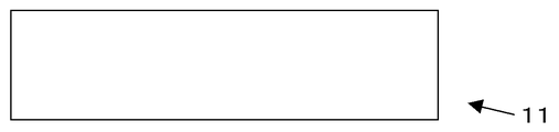
まず、図1の工程1や図2に示す様に、P型シリコン単結晶基板11を準備する。
この時準備するP型シリコン単結晶基板は、導電型がP型であること以外は特に限定されず、一般的に用いられているものであれば良い。例えばP型ドーパントをドープしてCZ法で育成したシリコン単結晶棒からスライスして作製したものを用いればよい。
この時準備するP型シリコン単結晶基板は、導電型がP型であること以外は特に限定されず、一般的に用いられているものであれば良い。例えばP型ドーパントをドープしてCZ法で育成したシリコン単結晶棒からスライスして作製したものを用いればよい。
ここで、この準備するP型シリコン単結晶基板は、後にN型エピタキシャル層が形成される主表面とは反対側の主表面に多結晶シリコン層が形成されたものか、若しくは該P型シリコン単結晶基板中に酸素析出核を有するものとすることができる。
これによって、P型シリコン単結晶基板のゲッタリング能力を容易に高いものとすることができ、後に半導体素子が形成される活性領域の金属不純物を容易に低減することができる。また、P型シリコン単結晶基板は後に除去するため、金属不純物をP型シリコン単結晶ごと除去できる。更にこれらの方法は一般的で容易に実施することができ、コスト的にも好適である。
従って、部分SOI構造のSOI基板で発生する結晶欠陥の問題のみならず、一般的なSOI基板で問題となる金属不純物の問題を容易に解決することができ、高品質且つ安価な半導体装置を製造することができる。
これによって、P型シリコン単結晶基板のゲッタリング能力を容易に高いものとすることができ、後に半導体素子が形成される活性領域の金属不純物を容易に低減することができる。また、P型シリコン単結晶基板は後に除去するため、金属不純物をP型シリコン単結晶ごと除去できる。更にこれらの方法は一般的で容易に実施することができ、コスト的にも好適である。
従って、部分SOI構造のSOI基板で発生する結晶欠陥の問題のみならず、一般的なSOI基板で問題となる金属不純物の問題を容易に解決することができ、高品質且つ安価な半導体装置を製造することができる。
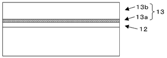
次に、エピタキシャル成長工程として、図1の工程2や図3に示す様に、P型シリコン単結晶基板11の主表面上に、N型エピタキシャル層12をエピタキシャル成長させる。このN型エピタキシャル層12の厚さは、エッチングストップ層として用いるものであるため、その厚さは5μm以下とすることが望ましい。
このように、P型シリコン単結晶基板11の主表面上に直接N型エピタキシャル層12を厚さ5μm以下でエピタキシャル成長させることができ、これによって、後の電気化学的エッチングによって除去する基板をP型シリコン単結晶基板のみとすることができ、不要な基板や層を形成せずに済み、効率的である。
このように、P型シリコン単結晶基板11の主表面上に直接N型エピタキシャル層12を厚さ5μm以下でエピタキシャル成長させることができ、これによって、後の電気化学的エッチングによって除去する基板をP型シリコン単結晶基板のみとすることができ、不要な基板や層を形成せずに済み、効率的である。
次に図1の工程3や図3に示す様に、N型エピタキシャル層12上に、半導体エピタキシャル層13を形成する。ここでは、N型低抵抗層13aと、N型高抵抗層13bを形成する。これでエピタキシャル成長工程は終了する。
また、このほかにも、図14(a)に示すように、P型シリコン単結晶基板31の直上のN型エピタキシャル層32の直上に、P型低抵抗層33aとP型高抵抗層33bを形成するものとすることができる。もしくは、図14(b)に示す様に、N型エピタキシャル層32’の直上に、P型低抵抗層33a’とN型低抵抗層33b’を形成するものとすることができる。また、図14(c)に示す様に、P型シリコン単結晶基板31の直上に、厚いN型エピタキシャル層32’’をエピタキシャル成長させるものとすることができる。あるいは、図14(d)に示す様に、N型エピタキシャル層32’’’の直上に、N型層33a’’’と、該N型層33a’’’中に部分的なP型低抵抗層33b’’’を形成するものとすることができる。
更に、N型エピタキシャル層等が形成された側とは反対側の表面に、ゲッタリングのための多結晶シリコン層34を設ける事もできる。
更に、N型エピタキシャル層等が形成された側とは反対側の表面に、ゲッタリングのための多結晶シリコン層34を設ける事もできる。
本発明の半導体装置の製造方法は、先に形成したN型エピタキシャル層12に正電圧を印加して、電気化学的エッチングによってP型シリコン単結晶基板11を除去するものである。従って、半導体素子形成領域となる半導体エピタキシャル層13は、作製する半導体素子に最適な構造を選択することができ、例えば上述のような構造とすることができるが、もちろんこれに限定されない。
その後、図1の工程4や図4に示す様に、半導体エピタキシャル層13に、半導体素子14を形成する。
また、半導体素子14の形成前または形成後に、半導体素子を誘電体分離するためのトレンチ15を形成し、その内部に絶縁材料、例えばシリコン酸化膜をトレンチ15の内部の表面に形成した後に多結晶シリコンを充填することが挙げられる。
このトレンチの深さは、N型エピタキシャル層に到達し、かつ貫通しない深さで形成することが望ましい。
更に、半導体素子14上に配線16aを内部に有する配線層16を形成する。
また、半導体素子14の形成前または形成後に、半導体素子を誘電体分離するためのトレンチ15を形成し、その内部に絶縁材料、例えばシリコン酸化膜をトレンチ15の内部の表面に形成した後に多結晶シリコンを充填することが挙げられる。
このトレンチの深さは、N型エピタキシャル層に到達し、かつ貫通しない深さで形成することが望ましい。
更に、半導体素子14上に配線16aを内部に有する配線層16を形成する。
図4は、ベース、エミッタ等の半導体素子14やトレンチ15、配線層16が形成された段階の図である。この段階は、基本的に一般的なバイポーラICの製造工程に沿った工程である。この工程でCMOSを形成するが、図では省略してある。
パッド電極(配線)の形成には、Au電極を用いた。その後Znを薄く全面に蒸着した。そのことにより、トレンチ分離された基板の各々の領域に所定電位を印加することを可能とした。
その後、図1の工程5や図5(a)に示す様に、石英等の保持基板17に配線層16と取り出し電極18が形成された面を貼り合わせる。
接着剤としては、紫外線剥離型のテープを用いると工程が複雑にならない。しかしこれに限定されることはない。
その後、図1の工程5や図5(a)に示す様に、石英等の保持基板17に配線層16と取り出し電極18が形成された面を貼り合わせる。
接着剤としては、紫外線剥離型のテープを用いると工程が複雑にならない。しかしこれに限定されることはない。
このように、電極配線が形成された側と保持基板を貼り合わせることができる。
これによって、保持基板を貼り合わせた後の工程において、電極配線を接地することによって、後の工程において、作業者等からの静電気によって半導体素子が破壊されることを抑制することができ、不良を低減することができる。また、容易にN型エピタキシャル層に正電圧を印加することができ、電気化学的エッチングが容易に行え、より都合がよい。尚、この時、電極を外部に取り出せるように配慮することがより望ましい。
これによって、保持基板を貼り合わせた後の工程において、電極配線を接地することによって、後の工程において、作業者等からの静電気によって半導体素子が破壊されることを抑制することができ、不良を低減することができる。また、容易にN型エピタキシャル層に正電圧を印加することができ、電気化学的エッチングが容易に行え、より都合がよい。尚、この時、電極を外部に取り出せるように配慮することがより望ましい。
また、保持基板17に、図5(b)に示す様に、表面に凹凸を有する低抵抗シリコン基板を用い、熱剥離型の接着剤で貼り合わせ、電極パッドとシリコン保持基板を電気的に導通させることも可能である。この場合、低抵抗シリコン基板自体が電極の役割を果たす。
これによって、より容易にN型エピタキシャル層に正電圧を印加でき、また静電気破壊から半導体素子を保護することができる。
これによって、より容易にN型エピタキシャル層に正電圧を印加でき、また静電気破壊から半導体素子を保護することができる。
その後、図1の工程6や図6に示す様に、P型シリコン単結晶基板11を、研削や研磨・エッチングのうち少なくとも1つを行って、その厚さを減ずることができる。
このように、電気化学的エッチングに比べて除去速度が速い研削・研磨・エッチングのうち少なくとも1つによってP型シリコン単結晶基板を薄膜化することによって、効率よくP型シリコン単結晶基板を除去することができ、除去工程の作業時間を短時間とすることができる。
尚、研削を行う場合は、研削仕上げ面が界面に極力平行になるようにするため、裏面側を基準にエピタキシャル成長後の基板を設置して研削を行うことが望ましい。
この研削・研磨・エッチングでのP型シリコン単結晶基板の除去量は、P型シリコン単結晶基板の厚さが50μm以下となる程度まで行うことが望ましい。
このように、電気化学的エッチングに比べて除去速度が速い研削・研磨・エッチングのうち少なくとも1つによってP型シリコン単結晶基板を薄膜化することによって、効率よくP型シリコン単結晶基板を除去することができ、除去工程の作業時間を短時間とすることができる。
尚、研削を行う場合は、研削仕上げ面が界面に極力平行になるようにするため、裏面側を基準にエピタキシャル成長後の基板を設置して研削を行うことが望ましい。
この研削・研磨・エッチングでのP型シリコン単結晶基板の除去量は、P型シリコン単結晶基板の厚さが50μm以下となる程度まで行うことが望ましい。
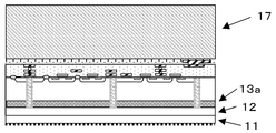
その後、図1の工程7や図7に示す様に、N型エピタキシャル層12に正電圧を印加して、電気化学的エッチングによってP型シリコン単結晶基板11の除去を行う。
これは例えば図12に示す様に、少なくとも半導体素子が形成された半導体エピタキシャル層を覆うようにして基板ホルダー25にP型シリコン単結晶基板11を保持した後、N型エピタキシャル層12をエッチストップ層として、アルカリ系の電解質溶液21に浸漬させて、N型エピタキシャル層12と作用極22との間に、N型エピタキシャル層12が正電位となるように、またトレンチで囲まれた領域どこでも、同等の正電圧が印加されるように電源24により電圧を印加して行うものとすることができる。
これは例えば図12に示す様に、少なくとも半導体素子が形成された半導体エピタキシャル層を覆うようにして基板ホルダー25にP型シリコン単結晶基板11を保持した後、N型エピタキシャル層12をエッチストップ層として、アルカリ系の電解質溶液21に浸漬させて、N型エピタキシャル層12と作用極22との間に、N型エピタキシャル層12が正電位となるように、またトレンチで囲まれた領域どこでも、同等の正電圧が印加されるように電源24により電圧を印加して行うものとすることができる。
アルカリ系の電解質溶液としてKOHを用いる場合を例に説明すると、KOHの水溶液(濃度40%前後)にN型エピタキシャル層に正の電圧をかけた状態で、電気化学的にエッチングを進める。
例えば、P型シリコン単結晶基板がKOH溶液に露出している間は、図13の右下に示す様に、基板表面は開放電圧(OCP)となり、通常のKOHへのどぶ漬け状態と同じにエッチングが進む。また、P型シリコン単結晶基板には空乏層ができて、界面から離れたところには電圧はかからない。空乏層の厚さは、印加する電圧が1Vの時には1μm程度である。
そしてP型シリコン単結晶基板がエッチングされ、正電圧が印加されたN型エピタキシャル層が溶液に露出すると、図13の右上に示す様に、その表面では陽極酸化が進み、厚い不導体膜が形成されてエッチングは行われなくなる。これによって、N型エピタキシャル層でエッチングをストップすることができる。
例えば、P型シリコン単結晶基板がKOH溶液に露出している間は、図13の右下に示す様に、基板表面は開放電圧(OCP)となり、通常のKOHへのどぶ漬け状態と同じにエッチングが進む。また、P型シリコン単結晶基板には空乏層ができて、界面から離れたところには電圧はかからない。空乏層の厚さは、印加する電圧が1Vの時には1μm程度である。
そしてP型シリコン単結晶基板がエッチングされ、正電圧が印加されたN型エピタキシャル層が溶液に露出すると、図13の右上に示す様に、その表面では陽極酸化が進み、厚い不導体膜が形成されてエッチングは行われなくなる。これによって、N型エピタキシャル層でエッチングをストップすることができる。
電気化学的エッチングを上述のような形態で行うことによって、P型シリコン単結晶基板のみを確実且つ容易に除去することができる。また、半導体素子が形成された半導体エピタキシャル層がエッチングされることを容易に抑制することができ、素子形成領域に不具合が発生することを抑制することができる。
尚、エッチングに用いるアルカリ電解質溶液は、KOH、濃度40%前後、液温50~60℃とすることが望ましい。しかしKOHや上記条件に限定されず、その他のアルカリ溶液、TMAH(テトラメチルアンモニウムハイドレート)等でも同じ作用効果を達成することができる。
次に、図1の工程8や図8に示す様に、露出させたN型エピタキシャル層12を研磨によって除去してトレンチ15の先端を露出させ、その後に、後述する絶縁膜を形成することができる。
これによって、トレンチと絶縁膜によって半導体素子を完全に誘電体分離でき、縦型素子や横型素子が同一チップに形成するのに非常に都合が良く、好適である。例えばデバイス領域の近傍に金属があり、ノイズやパワートランジスタの発熱による素子の誤動作にも高い耐性を有する集積回路を実現することができる。
これによって、トレンチと絶縁膜によって半導体素子を完全に誘電体分離でき、縦型素子や横型素子が同一チップに形成するのに非常に都合が良く、好適である。例えばデバイス領域の近傍に金属があり、ノイズやパワートランジスタの発熱による素子の誤動作にも高い耐性を有する集積回路を実現することができる。
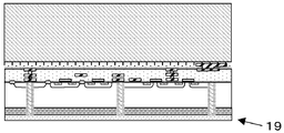
その後、図1の工程9や図9に示す様に、露出させた面に対して絶縁膜19を形成する。
この絶縁層の形成も後述する裏面電極の形成と同様に、蒸着、スパッター等の低温工程とすることが好ましい。例えば、スパッター、プラズマCVDや蒸着によってSiO2やSiNを形成することができる。
何れの手法で絶縁層を形成するにしろ、露出させたN型エピタキシャル層または研磨面は、絶縁層形成前に異物、不純物等が除去されることが望ましい。また、低温処理においても十分な接着力を確保するための表面処理が為されることがより望ましい。そのためには、例えば、枚葉式の洗浄機を用いて、洗浄することができる。
この絶縁層の形成も後述する裏面電極の形成と同様に、蒸着、スパッター等の低温工程とすることが好ましい。例えば、スパッター、プラズマCVDや蒸着によってSiO2やSiNを形成することができる。
何れの手法で絶縁層を形成するにしろ、露出させたN型エピタキシャル層または研磨面は、絶縁層形成前に異物、不純物等が除去されることが望ましい。また、低温処理においても十分な接着力を確保するための表面処理が為されることがより望ましい。そのためには、例えば、枚葉式の洗浄機を用いて、洗浄することができる。
また、接着力を向上するため、絶縁層形成後にパルス的アニールを行ってもよい。
このように、露出させたN型エピタキシャル層または研磨面はデバイス、デバイス動作に関係する領域を形成するので、素子の信頼性の確保等のためにも、清浄度の確保やダメージの抑制を配慮することが求められる。
このように、露出させたN型エピタキシャル層または研磨面はデバイス、デバイス動作に関係する領域を形成するので、素子の信頼性の確保等のためにも、清浄度の確保やダメージの抑制を配慮することが求められる。
そして、図1の工程10や図10に示す様に、絶縁膜19のうち、縦型素子とする半導体素子が形成された領域に対応する位置の絶縁膜を除去する窓明けを行い、窓明け部19aを形成する。これによって、素子の両側に電極が形成できるようになり、大量の電流を流すのに適した構造となる。
ここで、この絶縁膜19の窓明け工程は、トレンチ15を合わせマークとして、フォトリソグラフィーによって行うことができる。合わせ精度を必要としない場合はスキージー印刷も利用できる。
このように、半導体素子を誘電体分離しているトレンチを合わせマークとしたフォトリソグラフィーによれば、絶縁膜の所望の位置に裏面電極を形成するための窓を明けることができ、縦型素子の品質を向上させることができる。
このように、半導体素子を誘電体分離しているトレンチを合わせマークとしたフォトリソグラフィーによれば、絶縁膜の所望の位置に裏面電極を形成するための窓を明けることができ、縦型素子の品質を向上させることができる。
次に、図1の工程11や図10に示す様に、先に形成した窓明け部19aに、裏面電極20を形成する。
この裏面電極の形成は、蒸着またはスパッターで行うのがよい。
このように、生産性の高い蒸着によって裏面電極を形成すれば、効率よく裏面電極を形成することができる。また、密着性の高い膜を形成することのできるスパッターによって裏面電極を形成すれば、良好な特性の電極を得ることができる。
この裏面電極の形成は、蒸着またはスパッターで行うのがよい。
このように、生産性の高い蒸着によって裏面電極を形成すれば、効率よく裏面電極を形成することができる。また、密着性の高い膜を形成することのできるスパッターによって裏面電極を形成すれば、良好な特性の電極を得ることができる。
その後、図1の工程12や図11に示す様に、半導体素子が貼り付けられた保持基板17の剥離若しくは除去を行うことができる。
この剥離・除去には、例えば、ガラス保持基板を通してレーザー光または紫外光を照射して該ガラス保持基板を剥離する手法がその例として挙げられる。
この段階で、デバイスのパターンが半導体装置表面に露出されることになる。
ここで、電極面側(表面)に蒸着されたZnを硫酸等で除去することが望ましい。
この剥離・除去には、例えば、ガラス保持基板を通してレーザー光または紫外光を照射して該ガラス保持基板を剥離する手法がその例として挙げられる。
この段階で、デバイスのパターンが半導体装置表面に露出されることになる。
ここで、電極面側(表面)に蒸着されたZnを硫酸等で除去することが望ましい。
その後、ダイサーを用いてダイシングを行いチップを形成することにより、完全分離型のパワーICチップ等の半導体装置10を製造することができる。また、ダイシングに先立ち、裏面電極上に半田層を形成してからダイシングすることで工程を安定化することが望ましい。
このような本発明の半導体装置の製造方法によって、電気化学的エッチングが行われた高平坦性の表面層に絶縁層や裏面電極等を形成することができ、また所望の厚さを有するものとすることができる。また、例えばゲッタリング能力を持ったP型シリコン単結晶基板の主表面にN型エピタキシャル層及び半導体素子を形成する半導体エピタキシャル層を形成することができるため、活性領域の金属不純物濃度を従来に比べて低いものとすることができる。
更に、トレンチアイソレーション構造のCMOS集積回路やパワー素子の半導体素子を形成し、保持基板の付加や、研削等とN型エピタキシャル層をエッチストップ層とした電気化学的エッチストップによるP型シリコン単結晶基板の除去、裏面側の絶縁膜形成及びパワー素子部の絶縁膜の窓明け、裏面電極の形成によって、部分SOI構造のSOI基板でなくても、横型素子と縦型素子が同一チップに形成された半導体装置を効率よく製造することができる。
そしてSOI基板ではなくエピタキシャルウエーハから製造することができ、従来に比べて安価なものとすることができる。
従って、金属不純物濃度の低い、高性能且つ安価なパワーICチップを製造することができる。
更に、トレンチアイソレーション構造のCMOS集積回路やパワー素子の半導体素子を形成し、保持基板の付加や、研削等とN型エピタキシャル層をエッチストップ層とした電気化学的エッチストップによるP型シリコン単結晶基板の除去、裏面側の絶縁膜形成及びパワー素子部の絶縁膜の窓明け、裏面電極の形成によって、部分SOI構造のSOI基板でなくても、横型素子と縦型素子が同一チップに形成された半導体装置を効率よく製造することができる。
そしてSOI基板ではなくエピタキシャルウエーハから製造することができ、従来に比べて安価なものとすることができる。
従って、金属不純物濃度の低い、高性能且つ安価なパワーICチップを製造することができる。
そして、例えば、半導体エピタキシャル層の構造をN/N+/P+/N/Pといった構造にすることにより、出力段のパワー素子をIGBTとすることができる。また半導体エピタキシャル層の構造をN/N+/N/Pとすれば出力段のパワー素子を容易にP-MOSにすることができるといったメリットがある。このように、作製する半導体素子に合わせて半導体エピタキシャル層を任意にエピタキシャル成長させればよく、非常に応用が利く製造方法となっている。
以下、実施例を示して本発明をより具体的に説明するが、本発明はこれに限定されるものではない。
(実施例)
図1に示す様な工程に従って、半導体装置を製造した。
まず、抵抗率5Ωcm、直径8インチ(200mm)のP型シリコン単結晶基板を準備した。
次に、トリクロロシランを原料ガスとして、1150℃、枚葉式の反応機を用い、まず、N型の抵抗率5Ωcm、厚さ3μmのN型エピタキシャル層を成長させた。その後、半導体エピタキシャル層として、N型の抵抗率0.05Ωcm、厚さ2.5μmのN型低抵抗層のエピタキシャル成長を行い、次に、N型の抵抗率2Ωcm、厚さ6μmのN型層をエピタキシャル成長させた。
(実施例)
図1に示す様な工程に従って、半導体装置を製造した。
まず、抵抗率5Ωcm、直径8インチ(200mm)のP型シリコン単結晶基板を準備した。
次に、トリクロロシランを原料ガスとして、1150℃、枚葉式の反応機を用い、まず、N型の抵抗率5Ωcm、厚さ3μmのN型エピタキシャル層を成長させた。その後、半導体エピタキシャル層として、N型の抵抗率0.05Ωcm、厚さ2.5μmのN型低抵抗層のエピタキシャル成長を行い、次に、N型の抵抗率2Ωcm、厚さ6μmのN型層をエピタキシャル成長させた。
その後、作製した半導体素子形成領域に、酸化膜をマスクとして、アイソレーション用トレンチをRIE(Reactive Ion Etching:反応性イオンエッチング)により形成し、トレンチ内の表面を酸化した後、多結晶シリコンでトレンチを埋めた。ここで、トレンチの深さは9.0μmとした。
そして、図4に示すような、N、PウエルLOCOS酸化膜、ゲート酸化膜、ゲート、ソース、ドレイン等を形成した。その後、図4に示す様な配線層を形成した。
そして、図4に示すような、N、PウエルLOCOS酸化膜、ゲート酸化膜、ゲート、ソース、ドレイン等を形成した。その後、図4に示す様な配線層を形成した。
そして、電極パッドが形成された表面に亜鉛を真空蒸着させた後、光変性型の樹脂を用いて石英基板と貼り合わせた。
その後、P型シリコン単結晶基板を除去するにあたって、まず、研削によって基板の厚さが50μm程度になるまで削った。この際、残ったP型シリコン単結晶基板の厚さのバラツキがプラスマイナス10%以下になるように制御した。
その後、P型シリコン単結晶基板を除去するにあたって、まず、研削によって基板の厚さが50μm程度になるまで削った。この際、残ったP型シリコン単結晶基板の厚さのバラツキがプラスマイナス10%以下になるように制御した。
その後、接着に用いた光変性型の樹脂に針状の白金電極を刺して亜鉛電極と導通させて、テフロン(登録商標)製の基板ホルダーに配線層を形成したP型シリコン単結晶基板を取り付け、液温50℃、濃度30%のKOH水溶液に、N型エピタキシャル層とP型シリコン単結晶基板との界面において、N型エピタキシャル層が+1.5Vになるように電位を印加した状態で浸漬させて、研削で残ったP型シリコン単結晶基板を電気化学エッチングによって除去した。
その後、KOH水溶液から基板ホルダーごと取り出し、研磨によりN型エピタキシャル層を除去した面にプラズマCVDによって厚さ2μmの酸化膜を形成した。そしてフォトリソグラフィーによるパターニング・エッチングによって、縦型素子とする半導体素子が形成された領域に対応する位置の酸化膜を除去した。
更に、裏面側に裏面電極としてAu-Sbを蒸着によって堆積させ、RTAによってオーミック性を確保した。
その後、石英基板側から紫外線を照射し、石英基板を半導体素子が形成された半導体エピタキシャル層から分離し、フロントエンドのデバイス工程を完了させた。
更に、裏面側に裏面電極としてAu-Sbを蒸着によって堆積させ、RTAによってオーミック性を確保した。
その後、石英基板側から紫外線を照射し、石英基板を半導体素子が形成された半導体エピタキシャル層から分離し、フロントエンドのデバイス工程を完了させた。
尚、電気化学エッチング後に、露出したN型エピタキシャル層の平坦度を評価した。その結果、厚さのバラツキは0.2~0.3μmであり、高い精度でP型シリコン単結晶基板を除去できたことが判った。尚、従来の研削・研磨・エッチングでは±1μm程度が限界であり、本発明の電気化学的エッチングが優れていることが確認できた。
なお、本発明は、上記実施形態に限定されるものではない。上記実施形態は例示であり、本発明の特許請求の範囲に記載された技術的思想と実質的に同一な構成を有し、同様な作用効果を奏するものは、いかなるものであっても本発明の技術的範囲に包含される。
Claims (12)
- 少なくとも、
導電型がP型のシリコン単結晶基板の一方の主表面に、エッチストップ層となる導電型がN型のN型エピタキシャル層と、半導体素子を形成するための半導体エピタキシャル層とをこの順にエピタキシャル成長させる工程と、
前記半導体素子を形成するための半導体エピタキシャル層に、前記半導体素子と、該半導体素子を誘電体分離するためのトレンチを形成する工程と、
該半導体素子が形成された側の表面に保持基板を貼り合わせる工程と、
前記N型エピタキシャル層に正電圧を印加して、該N型エピタキシャル層をエッチストップ層として電気化学的エッチングにより前記P型シリコン単結晶基板を除去する工程と、
該露出した表面に絶縁膜を形成する工程と、
該絶縁膜のうち、縦型素子とする前記半導体素子が形成された領域に対応する位置の絶縁膜を除去する窓明けを行う工程と、
該窓明け部に、裏面電極を形成する工程とを有することを特徴とする半導体装置の製造方法。
- 前記エピタキシャル成長工程は、前記P型シリコン単結晶基板の直上に前記N型エピタキシャル層を厚さ5μm以下でエピタキシャル成長させることを特徴とする請求項1に記載の半導体装置の製造方法。
- 前記P型シリコン単結晶基板は、前記N型エピタキシャル層が形成された主表面とは反対側の主表面に多結晶シリコン層が形成されたものか、若しくは該P型シリコン単結晶基板中に酸素析出核を有するものとすることを特徴とする請求項1または請求項2に記載の半導体装置の製造方法。
- 前記電気化学的エッチングは、少なくとも前記半導体素子を形成した半導体エピタキシャル層を覆う基板ホルダーに前記P型シリコン単結晶基板を保持した後、前記N型エピタキシャル層をエッチストップ層として、前記トレンチ毎に正電圧が印加されるようにアルカリ電解質溶液に浸漬させて行うものとすることを特徴とする請求項1ないし請求項3のいずれか1項に記載の半導体装置の製造方法。
- 前記半導体素子形成工程後、前記貼り合わせ工程前に、前記半導体素子上に電極配線を形成し、その後該電極配線が形成された側の表面に前記保持基板を貼り合わせることを特徴とする請求項1ないし請求項4のいずれか1項に記載の半導体装置の製造方法。
- 前記保持基板は、前記貼り合わせ面から逆側の表面に達する電極を有することを特徴とする請求項5に記載の半導体装置の製造方法。
- 前記P型シリコン単結晶基板の除去工程は、該P型シリコン単結晶基板に研削・研磨・エッチングのうち少なくとも1つを行った後、前記電気化学的エッチングを行うものとすることを特徴とする請求項1ないし請求項6のいずれか1項に記載の半導体装置の製造方法。
- 前記P型シリコン単結晶基板の除去工程の後、露出した電気化学的エッチストップ面に対して研磨を行って前記トレンチの先端を露出させ平坦化し、その後前記絶縁膜を形成することを特徴とする請求項1ないし請求項7のいずれか1項に記載の半導体装置の製造方法。
- 前記絶縁膜の窓明け工程は、前記トレンチを合わせマークとして、フォトリソグラフィーによって行うことを特徴とする請求項1ないし請求項8のいずれか1項に記載の半導体装置の製造方法。
- 前記裏面電極の形成を、蒸着、スパッターのいずれかの方法で行うことを特徴とする請求項1ないし請求項9のいずれか1項に記載の半導体装置の製造方法。
- 前記裏面電極形成工程の後、前記保持基板を剥離または除去することを特徴とする請求項1ないし請求項10のいずれか1項に記載の半導体装置の製造方法。
- 前記エピタキシャル成長工程は、前記N型エピタキシャル層の直上に、P型低抵抗層とN型低抵抗層を形成するものとし、前記P型シリコン単結晶基板の除去工程の後、露出した前記N型エピタキシャル層を除去し、前記半導体素子が形成された側の裏面である前記P型低抵抗層から電極を取り出すことを特徴とする請求項1ないし請求項11のいずれか1項に記載の半導体装置の製造方法。
Applications Claiming Priority (2)
| Application Number | Priority Date | Filing Date | Title |
|---|---|---|---|
| JP2009193420A JP2011044667A (ja) | 2009-08-24 | 2009-08-24 | 半導体装置の製造方法 |
| JP2009-193420 | 2009-08-24 |
Publications (1)
| Publication Number | Publication Date |
|---|---|
| WO2011024358A1 true WO2011024358A1 (ja) | 2011-03-03 |
Family
ID=43627481
Family Applications (1)
| Application Number | Title | Priority Date | Filing Date |
|---|---|---|---|
| PCT/JP2010/003857 Ceased WO2011024358A1 (ja) | 2009-08-24 | 2010-06-10 | 半導体装置の製造方法 |
Country Status (2)
| Country | Link |
|---|---|
| JP (1) | JP2011044667A (ja) |
| WO (1) | WO2011024358A1 (ja) |
Cited By (4)
| Publication number | Priority date | Publication date | Assignee | Title |
|---|---|---|---|---|
| WO2015037095A1 (ja) * | 2013-09-11 | 2015-03-19 | 富士電機株式会社 | 半導体装置 |
| CN111902915A (zh) * | 2018-03-23 | 2020-11-06 | 法语天主教鲁汶大学 | 对衬底进行电化学处理的方法和集成电路装置 |
| TWI747200B (zh) * | 2019-09-24 | 2021-11-21 | 台灣積體電路製造股份有限公司 | 半導體晶圓及其形成方法與集成晶片 |
| CN113964087A (zh) * | 2019-10-21 | 2022-01-21 | 新唐科技日本株式会社 | 半导体装置及单片化方法 |
Citations (8)
| Publication number | Priority date | Publication date | Assignee | Title |
|---|---|---|---|---|
| JPH02228049A (ja) * | 1989-02-28 | 1990-09-11 | Nec Corp | 半導体装置の製造方法 |
| JPH0738102A (ja) * | 1993-07-20 | 1995-02-07 | Fuji Electric Co Ltd | 高耐圧半導体装置の製造方法 |
| JPH08507904A (ja) * | 1993-03-17 | 1996-08-20 | ブリティッシュ・テクノロジー・グループ・リミテッド | 半導体構造およびその製造方法 |
| JPH10335305A (ja) * | 1996-09-02 | 1998-12-18 | Denso Corp | 半導体装置の製造方法 |
| JP2001111014A (ja) * | 1999-08-30 | 2001-04-20 | Lucent Technol Inc | ボンデッドウエハおよびその製造方法およびそれにより製造される集積回路 |
| JP2001127149A (ja) * | 1999-10-26 | 2001-05-11 | Denso Corp | 半導体装置およびその製造方法 |
| JP2004510329A (ja) * | 2000-09-21 | 2004-04-02 | ケンブリッジ セミコンダクター リミテッド | 半導体デバイスおよび半導体デバイスを形成する方法 |
| JP2008166705A (ja) * | 2006-12-06 | 2008-07-17 | Denso Corp | 半導体装置およびその製造方法 |
-
2009
- 2009-08-24 JP JP2009193420A patent/JP2011044667A/ja active Pending
-
2010
- 2010-06-10 WO PCT/JP2010/003857 patent/WO2011024358A1/ja not_active Ceased
Patent Citations (8)
| Publication number | Priority date | Publication date | Assignee | Title |
|---|---|---|---|---|
| JPH02228049A (ja) * | 1989-02-28 | 1990-09-11 | Nec Corp | 半導体装置の製造方法 |
| JPH08507904A (ja) * | 1993-03-17 | 1996-08-20 | ブリティッシュ・テクノロジー・グループ・リミテッド | 半導体構造およびその製造方法 |
| JPH0738102A (ja) * | 1993-07-20 | 1995-02-07 | Fuji Electric Co Ltd | 高耐圧半導体装置の製造方法 |
| JPH10335305A (ja) * | 1996-09-02 | 1998-12-18 | Denso Corp | 半導体装置の製造方法 |
| JP2001111014A (ja) * | 1999-08-30 | 2001-04-20 | Lucent Technol Inc | ボンデッドウエハおよびその製造方法およびそれにより製造される集積回路 |
| JP2001127149A (ja) * | 1999-10-26 | 2001-05-11 | Denso Corp | 半導体装置およびその製造方法 |
| JP2004510329A (ja) * | 2000-09-21 | 2004-04-02 | ケンブリッジ セミコンダクター リミテッド | 半導体デバイスおよび半導体デバイスを形成する方法 |
| JP2008166705A (ja) * | 2006-12-06 | 2008-07-17 | Denso Corp | 半導体装置およびその製造方法 |
Cited By (7)
| Publication number | Priority date | Publication date | Assignee | Title |
|---|---|---|---|---|
| WO2015037095A1 (ja) * | 2013-09-11 | 2015-03-19 | 富士電機株式会社 | 半導体装置 |
| JPWO2015037095A1 (ja) * | 2013-09-11 | 2017-03-02 | 富士電機株式会社 | 半導体装置 |
| US9893055B2 (en) | 2013-09-11 | 2018-02-13 | Fuji Electric Co., Ltd. | Semiconductor device including an insulated gate bipolar transistor and a circuit configured to control the insulated gate bipolar transistor provided on the same semiconductor substrate |
| CN111902915A (zh) * | 2018-03-23 | 2020-11-06 | 法语天主教鲁汶大学 | 对衬底进行电化学处理的方法和集成电路装置 |
| CN111902915B (zh) * | 2018-03-23 | 2024-02-02 | 法语天主教鲁汶大学 | 对衬底进行电化学处理的方法和集成电路装置 |
| TWI747200B (zh) * | 2019-09-24 | 2021-11-21 | 台灣積體電路製造股份有限公司 | 半導體晶圓及其形成方法與集成晶片 |
| CN113964087A (zh) * | 2019-10-21 | 2022-01-21 | 新唐科技日本株式会社 | 半导体装置及单片化方法 |
Also Published As
| Publication number | Publication date |
|---|---|
| JP2011044667A (ja) | 2011-03-03 |
Similar Documents
| Publication | Publication Date | Title |
|---|---|---|
| CN101861652B (zh) | 含有(110)-取向硅的半导体器件 | |
| US7244990B2 (en) | Semiconductor device | |
| JP5655931B2 (ja) | 半導体装置の製造方法 | |
| US20120012972A1 (en) | Single-crystal silicon substrate, soi substrate, semiconductor device, display device, and manufacturing method of semiconductor device | |
| US6384422B2 (en) | Method for manufacturing semiconductor device and ultrathin semiconductor device | |
| JP3944087B2 (ja) | 素子形成用基板の製造方法 | |
| CN101926005B (zh) | 用于消除多晶硅/金属板电容器中的工艺相关缺陷的结构及方法 | |
| JP2011044667A (ja) | 半導体装置の製造方法 | |
| JP2005082870A (ja) | 積層基板の洗浄方法および基板の貼り合わせ方法 | |
| TW201729339A (zh) | 絕緣體上半導體型基板 | |
| KR102817685B1 (ko) | 반도체-온-절연체(soi) 기판을 형성하는 방법 | |
| JP5386862B2 (ja) | 半導体装置の製造方法 | |
| JP2000031439A (ja) | Soi基板およびその製造方法 | |
| JP2001320033A (ja) | 半導体部材の製造方法およびそれを用いた半導体部材、半導体装置 | |
| JP4834309B2 (ja) | 半導体装置の製造方法 | |
| US11710656B2 (en) | Method of forming semiconductor-on-insulator (SOI) substrate | |
| US20140199823A1 (en) | Method for manufacturing semiconductor device | |
| JP2008091935A (ja) | 集積回路 | |
| KR20070062149A (ko) | 레이저유도 에피택셜 성장 및 cmp를 이용한 다층트랜지스터의 형성 방법 | |
| KR100722523B1 (ko) | 웨이퍼 표면 식각 방법 | |
| CN120511232A (zh) | 形成接合到加工衬底的薄半导体层的工艺和包括该薄半导体层的电子器件 | |
| JPH11329968A (ja) | 半導体基材とその作製方法 | |
| JPS632374A (ja) | 半導体記憶装置の製造法 | |
| JP2004172362A (ja) | 半導体ウエハの不純物除去方法、半導体ウエハアセンブリ、半導体ウエハ、及び半導体デバイス | |
| JP2008053410A (ja) | 半導体装置の製造方法 |
Legal Events
| Date | Code | Title | Description |
|---|---|---|---|
| 121 | Ep: the epo has been informed by wipo that ep was designated in this application |
Ref document number: 10811417 Country of ref document: EP Kind code of ref document: A1 |
|
| NENP | Non-entry into the national phase |
Ref country code: DE |
|
| 122 | Ep: pct application non-entry in european phase |
Ref document number: 10811417 Country of ref document: EP Kind code of ref document: A1 |