WO2011024348A1 - 有機エレクトロルミネッセンス素子、有機エレクトロルミネッセンス表示装置、有機エレクトロルミネッセンス照明装置、および有機エレクトロルミネッセンス素子の製造方法 - Google Patents
有機エレクトロルミネッセンス素子、有機エレクトロルミネッセンス表示装置、有機エレクトロルミネッセンス照明装置、および有機エレクトロルミネッセンス素子の製造方法 Download PDFInfo
- Publication number
- WO2011024348A1 WO2011024348A1 PCT/JP2010/002902 JP2010002902W WO2011024348A1 WO 2011024348 A1 WO2011024348 A1 WO 2011024348A1 JP 2010002902 W JP2010002902 W JP 2010002902W WO 2011024348 A1 WO2011024348 A1 WO 2011024348A1
- Authority
- WO
- WIPO (PCT)
- Prior art keywords
- organic
- region
- light emitting
- acceptor
- donor
- Prior art date
- Legal status (The legal status is an assumption and is not a legal conclusion. Google has not performed a legal analysis and makes no representation as to the accuracy of the status listed.)
- Ceased
Links
Images


Classifications
-
- H—ELECTRICITY
- H05—ELECTRIC TECHNIQUES NOT OTHERWISE PROVIDED FOR
- H05B—ELECTRIC HEATING; ELECTRIC LIGHT SOURCES NOT OTHERWISE PROVIDED FOR; CIRCUIT ARRANGEMENTS FOR ELECTRIC LIGHT SOURCES, IN GENERAL
- H05B33/00—Electroluminescent light sources
- H05B33/10—Apparatus or processes specially adapted to the manufacture of electroluminescent light sources
-
- H—ELECTRICITY
- H10—SEMICONDUCTOR DEVICES; ELECTRIC SOLID-STATE DEVICES NOT OTHERWISE PROVIDED FOR
- H10K—ORGANIC ELECTRIC SOLID-STATE DEVICES
- H10K50/00—Organic light-emitting devices
- H10K50/10—OLEDs or polymer light-emitting diodes [PLED]
- H10K50/14—Carrier transporting layers
- H10K50/15—Hole transporting layers
- H10K50/155—Hole transporting layers comprising dopants
-
- H—ELECTRICITY
- H10—SEMICONDUCTOR DEVICES; ELECTRIC SOLID-STATE DEVICES NOT OTHERWISE PROVIDED FOR
- H10K—ORGANIC ELECTRIC SOLID-STATE DEVICES
- H10K50/00—Organic light-emitting devices
- H10K50/10—OLEDs or polymer light-emitting diodes [PLED]
- H10K50/14—Carrier transporting layers
- H10K50/16—Electron transporting layers
- H10K50/165—Electron transporting layers comprising dopants
-
- H—ELECTRICITY
- H10—SEMICONDUCTOR DEVICES; ELECTRIC SOLID-STATE DEVICES NOT OTHERWISE PROVIDED FOR
- H10K—ORGANIC ELECTRIC SOLID-STATE DEVICES
- H10K2101/00—Properties of the organic materials covered by group H10K85/00
- H10K2101/80—Composition varying spatially, e.g. having a spatial gradient
Definitions
- the present invention relates to an organic electroluminescence element, an organic electroluminescence display device, an organic electroluminescence lighting device, and a method for manufacturing the organic electroluminescence element that achieve high brightness, high efficiency, and long life with a simple structure.
- a non-self-luminous liquid crystal display LCD
- a self-luminous plasma display PDP
- an inorganic electroluminescence (inorganic EL) display or an organic electroluminescence (hereinafter referred to as “organic EL” or “ A display or the like is also known.
- organic EL organic electroluminescence
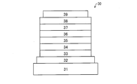
- FIG. 5 is a schematic view showing a configuration of a conventional organic electroluminescence element.
- Non-Patent Document 1 describes an organic EL element having a simple structure called “homojunction” using a bipolar material exhibiting high charge mobility.
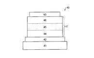
- FIG. 6 is a schematic view showing a configuration of a conventional organic electroluminescence element.
- the organic EL element 40 of Non-Patent Document 1 includes a charge transporting light-emitting layer 47 containing a charge transporting material between an anode 42 and a cathode 43 provided on a substrate 41. It is a simple structure that is pinched.
- the charge transporting light emitting layer 47 includes an acceptor doped region 44 doped with an acceptor, a light emitting material doped region 45 doped with a light emitting material, and a donor doped region 46 doped with a donor.
- Non-Patent Document 1 describes that an organic EL element having such a simple structure emits EL by both fluorescence and phosphorescence and emits light of three primary colors of blue, green, and red.
- the organic EL element 40 having a simplified layer structure has a problem that the light emission efficiency or the luminance decreases with time. This is because the regions 44 and 46 doped with acceptor or donor at a high concentration are in contact with the region 45 doped with an organic light emitting material in the charge transporting light emitting layer 47.
- the acceptor's HOMO (Highest Occupied Molecular Orbital) level is lower than the HOMO level of both charge transport materials. Therefore, as in Non-Patent Document 1, when the region 44 doped with a high concentration of acceptor is in contact with the region 45 doped with an organic light emitting material, the difference between the two HOMO levels is large, so that the injection is performed from the anode. Hole cannot efficiently propagate through the acceptor doped region 44 to both charge transporting materials in the light emitting material doped region 45.
- the donor's LUMO (Lowest Unoccupied Molecular Orbital) level is higher than the LUMO level of both charge transport materials.
- the region 44 doped with a high concentration is in contact with the region 45 doped with an organic light emitting material, the difference in the LUMO level between the two is large, and electrons injected from the cathode enter the donor doped region 46. Therefore, the light cannot be efficiently propagated to the charge transport material in the light emitting material doped region 45. Therefore, since holes and electrons are not efficiently recombined in the light emitting material doped region 45, the luminance, light emission efficiency, and lifetime are inferior to those of an organic EL element having a multilayer structure.
- the present invention has been made in view of the above problems, and an object thereof is to provide an organic EL element having a simple structure, high luminance, high efficiency, and long life.
- the organic electroluminescence device is An anode, a cathode, and an organic layer containing both charge transport materials between the anode and the cathode;
- the organic layer is located on the anode side and is doped with an acceptor-doped first region, located on the cathode side and doped with a donor, the first region and the second region.
- a third region doped with an organic light emitting material The acceptor is graded so that the concentration decreases from the anode side toward the third region in the first region,
- the donor is characterized in that a gradient is given in the second region so that the concentration decreases from the cathode side toward the third region.
- the organic electroluminescent element (henceforth an "organic EL element") of this invention has an organic layer provided between the anode and the cathode containing both charge transport materials, and the anode side Has a first region doped with an acceptor and a second region doped with a donor on the cathode side. Further, in the first region, the concentration gradient of the acceptor with respect to the charge transporting material of the acceptor is set so as to decrease from the anode side, and in the second region, with respect to the charge transporting material of the donor with respect to the charge transporting material. A concentration gradient is provided so that the concentration decreases from the cathode side.
- the concentration of the acceptor is highest on the side in contact with the anode, and the concentration decreases toward the center of the organic layer doped with the organic light emitting material. For this reason, the holes propagating through the acceptor are efficiently propagated to the charge transporting material, and finally the holes are completely transported in the charge transporting material in the third region where the organic light emitting material is doped. Can be propagated in.
- the side in contact with the cathode has the highest donor concentration, and the concentration decreases toward the center of the organic layer doped with the organic light emitting material. For this reason, in the third region in which the electrons propagating through the donor are efficiently propagated to the both charge transporting materials and finally doped with the organic light emitting material, the electrons are completely contained in the both charge transporting materials. It can be propagated.
- the organic EL device of the present invention holes and electrons can be smoothly transported to the third region doped with the organic light emitting material, and can be efficiently recombined in the region. Luminance and highly efficient light emission can be maintained over a long period of time.
- the organic electroluminescence display device is characterized by comprising display means in which the organic electroluminescence element according to the present invention is formed on a thin film transistor substrate in order to solve the above-mentioned problems.
- the organic electroluminescence lighting device includes the organic electroluminescence element according to the present invention.
- the organic electroluminescence element capable of efficiently injecting and transporting holes and electrons to the region doped with the organic light emitting material is provided, it has high luminance, high efficiency, and long length.
- a lifetime display device and a lighting device can be provided.
- the organic electroluminescence device manufacturing method includes an evaporation source filled with an acceptor, an organic light emitting material, a donor, and a charge transport material, and is installed in parallel.
- the acceptor, the organic light emitting material, the donor, and the both charge transporting materials are vapor deposited from the vapor deposition sources onto the substrate.
- the material when the substrate is moved along the deposition sources (also referred to as supply means) of the acceptor, the organic light emitting material, and the donor that are installed in advance, the material is supplied from each supply means.
- the deposition sources also referred to as supply means
- the vapor deposition method is used as the supply method, each material can be vapor-deposited on the substrate only by the operation of moving the substrate along the respective supply means. Therefore, the organic electroluminescence element according to the present invention can be efficiently produced.
- the organic electroluminescent device includes an anode, a cathode, and an organic layer containing both charge transport materials between the anode and the cathode, the organic layer is located on the anode side, and an acceptor is provided A first doped region, a second region doped with a donor and doped with a donor, located between the first region and the second region, and an organic light emitting material And the acceptor is graded so that the concentration decreases from the anode side toward the third region in the first region, and the donor In the second region, a gradient is given so that the concentration decreases from the cathode side toward the third region. Therefore, an organic EL element with a simple structure, high luminance, high efficiency, and long life can be provided.
- organic electroluminescence element An embodiment of the organic electroluminescence element according to the present invention will be described below with reference to FIGS.
- organic electroluminescence element is also simply referred to as “organic EL element”.
- FIG. 1 is a schematic view showing a configuration of an organic EL element according to the first embodiment of the present invention.
- the graph shown in FIG. 1 has shown the density
- the straight line shown and the straight line indicating the concentration of both charge transporting materials intersecting with the straight line indicate the acceptor concentration and the both charge transporting material concentrations in the acceptor region 6 described later.
- the organic EL element 1 includes an anode 3, a cathode 4, and an organic EL layer (organic layer) 5.
- Organic EL element 1 is a light emitting element having a single organic EL layer 5. Specifically, the organic EL element 1 includes a single organic EL layer 5 between an anode 3 and a cathode 4 provided on a substrate 2.
- the anode 3 is an electrode that injects holes into the organic EL layer 5 by applying a voltage.
- the cathode 4 is an electrode that injects electrons into the organic EL layer 5 when a voltage is applied.
- the anode 3 is directly laminated on the substrate 2, but the cathode 4 may be provided on the substrate 2. That is, when one electrode of the organic EL element 1 is the anode 3, the other electrode may be disposed so as to function as a pair so that the other electrode becomes the cathode 4.
- the organic EL layer 5 is a single-layer light emitting layer containing both charge transport materials. That is, the organic EL layer 5 transports holes and electrons (hereinafter collectively referred to as “charge” or “carrier”) and emits light by recombination of these charges.
- charge holes and electrons
- the organic EL layer 5 is located on the anode 3 side of the organic EL layer 5 and is an acceptor region (first region) 6 doped with an acceptor, and is located on the cathode 4 side and is doped with a donor region. (Second region) 8 and a light emitting region (third region) 7 that is located between the acceptor region 6 and the donor region 8 and is doped with an organic light emitting material.
- the organic EL layer 5 is a single light emitting layer provided between the anode 3 and the cathode 4.
- the acceptor region 6 located on the anode 3 side and the donor region 8 located on the cathode 4 side.
- a light emitting region 7 located between the acceptor region 6 and the donor region 8.
- the organic EL device according to the present invention is not limited to this configuration.
- the charge transporting material region in which the acceptor and the organic light emitting material are not included between the acceptor region 6 and the light emitting region 7 is used. May be included.
- a charge transporting material region that does not contain the donor and the organic light emitting material may be included between the donor region 8 and the light emitting region 7.
- the organic EL layer 5 includes both charge transporting materials and may be doped with an acceptor, a donor, and an organic light emitting material. However, the organic EL layer 5 is not limited to this. These materials may be dispersed.
- the conductivity of the charge can be sufficiently improved by changing the band structure of the region. Therefore, it is not necessary to provide a hole transport layer or an electron transport layer between each electrode and the organic EL layer 5.
- the organic EL layer 5 is composed of a hole / electron injection layer and a hole / electron transport layer. Therefore, it is possible to emit light with high brightness and high efficiency with a simple structure.
- the range of the ratio of the thickness in the acceptor region 6 of the organic EL layer 5 is not particularly limited.
- the range is 90 from the anode 3 side. It suffices that it is within the range of 70 from the anode 3 side.
- the range of the ratio of the thickness of the organic EL layer 5 in the donor region 8 is not particularly limited.
- the thickness range is 90 from the cathode 4 side. It may be sufficient, and it is more preferable that it is the range of 70 from the cathode 4 side.
- region 8 shown here shows the range of the ratio which each can take, and the ratio of the thickness of the acceptor area
- the range of the ratio of the thickness of the organic EL layer 5 in the light emitting region 7 is not particularly limited.
- the center of the organic EL layer 5 is From the center of the organic EL layer 5 is more preferable.
- a concentration gradient is set so that the acceptor concentration decreases from the anode 3 side toward the light emitting region 7, and in the donor region 8, the donor's concentration from the cathode 4 side toward the light emitting region 7 is increased. It is sufficient that a concentration gradient is provided so that the concentration is lowered.
- the concentration gradient may be continuous or stepwise.
- the acceptor concentration is highest on the side in contact with the anode, and the concentration decreases toward the light emitting region 7 doped with the organic light emitting material. For this reason, the holes propagating through the acceptor are efficiently propagated to the both charge transport materials, and finally the holes are completely contained in the both charge transport materials in the light emitting region 7 doped with the organic light emitting material. Can be propagated to.
- the side in contact with the cathode 4 has the highest donor concentration, and the concentration decreases toward the light emitting region 7 doped with the organic light emitting material. For this reason, the electrons propagating through the donor are efficiently propagated to the both charge transport materials, and finally the electrons are completely propagated into the both charge transport materials in the light emitting region 7 doped with the organic light emitting material. Can be made.
- the acceptor concentration in the acceptor region 6 is not particularly limited, and may be, for example, in the range of 0.1 to 40 wt /%, and more preferably in the range of 1 to 20 wt /%.
- the donor concentration in the donor region 8 is not particularly limited and may be, for example, in the range of 0.1 to 40 wt /%, and more preferably in the range of 1 to 20 wt /%.
- acceptor concentration gradient in the acceptor region 6 and the donor concentration gradient in the donor region 8 may be set so as to decrease toward the light emitting region 7, but are more preferably exponentially applied. .
- the acceptor concentration gradient in the acceptor region 6 is set so that the concentration decreases from the anode 3 side toward the light emitting region 7 in proportion to the square of the distance from the anode 3.
- the concentration gradient may be set so that the concentration decreases from the cathode 4 side toward the light emitting region 7 in proportion to the square of the distance from the cathode 4.
- a concentration gradient may be provided.
- the concentration of the organic light emitting material increases from the side facing the acceptor region 6 and the donor region 8 toward the center.
- the concentration of the organic light emitting material is low. Therefore, the holes propagating through the acceptor can be efficiently propagated to the charge transporting material in the interface region, and finally the holes are completely propagated in the charge transporting material in the light emitting region 7. Can do.
- the concentration of the organic light emitting material is low. Therefore, the electrons propagating through the donor can be efficiently propagated in the charge transporting material in the interface region, and finally the electrons can be propagated completely in the charge transporting material in the light emitting region 7. it can.
- the concentration of the organic light emitting material in the light emitting region 7 is not particularly limited, and may be in the range of 0.1 to 30 wt /%, for example, in the vicinity of the center of the light emitting region 7 and in the range of 1 to 20 wt /%. It is more preferable that
- the film thickness of the organic EL layer 5 is not particularly limited, and may be, for example, in the range of 1 to 1,000 nm, but more preferably in the range of 10 to 200 nm.
- the film thickness is 10 nm or more, pixel defects caused by foreign matters such as dust can be prevented.
- the film thickness is 200 nm or less, an increase in driving voltage caused by the resistance component of the organic EL layer 5 can be suppressed.
- Both charge transport materials are classified as low-molecular materials or high-molecular materials.
- the charge transporting material that can be used for the organic EL layer 5 is not particularly limited.
- a known charge transporting material used for the organic EL can be used.
- low molecular weight materials include benzofuran derivatives such as bis (carbazoyl) benzodifuran (CZBDF), cyclopentadiene derivatives, tetraphenylbutadiene derivatives, triphenylamine derivatives, oxadiazole derivatives, bathophenanthroline derivatives, pyrazoloquinoline derivatives, styryl.
- benzofuran derivatives such as bis (carbazoyl) benzodifuran (CZBDF), cyclopentadiene derivatives, tetraphenylbutadiene derivatives, triphenylamine derivatives, oxadiazole derivatives, bathophenanthroline derivatives, pyrazoloquinoline derivatives, styryl.
- Polymer materials include poly (oxadiazole) (Poly-OXZ), polystyrene derivative (PSS), polyaniline-camphor sulfonic acid (PANI-CSA), poly (triphenylamine-oxadiazole) derivative ( Poly-TPD-OXD), poly (carbazole-triazole) derivatives (Poly-Cz-TAZ) and the like.
- the singlet excitation level having a higher excitation level than the triplet excitation level (T 1 ) of the phosphorescent light-emitting material is preferable to use a charge transporting material having a position (S 1 ). That is, it is more preferable that the relationship of S 1 (both charge transport materials)> T 1 (organic light emitting material) is satisfied. Therefore, it is more preferable to use a carbazole group, a triazole group, or a benzofuran group having a high excitation level and a high hole mobility as the both charge transporting material.
- the organic EL layer 5 when each material mentioned above is disperse
- a polymeric material polyvinylcarbazole
- examples of the inorganic material include polycarbonate and polyethylene terephthalate.
- examples of the inorganic material include silicon oxide and tin oxide.
- the acceptor is not particularly limited, and a known acceptor material used for organic EL can be used.
- acceptor materials include gold (Au), platinum (Pt), tungsten (W), iridium (Ir), POCl 3 , AsF 6 , chlorine (Cl), barium (Br), iodine (I), and vanadium oxide.
- Inorganic materials such as (V 2 O 5 ) and molybdenum oxide (MoO 2 ), TCNQ (7,7,8,8, -tetracyanoquinodimethane), TCNQF 4 (tetrafluorotetracyanoquinodimethane), TCNE ( Compounds having a cyano group such as tetracyanoethylene), HCNB (hexacyanobutadiene), DDQ (dicyclodicyanobenzoquinone), compounds having a nitro group such as TNF (trinitrofluorenone), DNF (dinitrofluorenone), fluoranyl, chloranil, Examples thereof include organic materials such as bromanyl.
- a compound having a cyano group such as TCNQ, TCNQF 4 , TCNE, HCNB, or DDQ.
- the donor is not particularly limited, and a known donor material used for a conventional organic EL element can be used.
- donor materials include alkali metals, alkaline earth metals, rare earth elements, Al (aluminum), Ag (silver), Cu (copper), In (indium) and other inorganic materials, anilines, phenylenediamines, and benzidine.
- donor materials in order to increase the carrier concentration more effectively, it is more preferable to use a compound having an aromatic tertiary amine skeleton, a condensed polycyclic compound, or an alkali metal.
- the organic light emitting material that can be used for the organic EL layer 5 is not particularly limited, and for example, a known organic light emitting material used for the organic EL can be used.
- organic light-emitting materials include fluorescent materials such as styryl derivatives, perylene, iridium complexes, coumarin derivatives, lumogen F red, dicyanomethylenepyran, phenoxazone, and porphyrin derivatives, and bis [(4,6-difluorophenyl) -pyridinato.
- a phosphorescent material As the organic light emitting material, it is more preferable to use a phosphorescent material as the organic light emitting material.
- the addition ratio of the acceptor material to the both charge transporting materials is, for example, preferably 0.1 to 50 wt%, and more preferably 1 to 20 wt%. Further, the ratio of the donor material added to both charge transport materials is, for example, preferably 0.1 to 50 wt%, and more preferably 1 to 20 wt%. Furthermore, the addition ratio of the organic light emitting material to both charge transporting materials is, for example, preferably 0.1 to 50 wt%, and more preferably 1 to 20 wt%.
- the addition ratio of the organic light emitting material to the both charge transport materials is smaller than the addition ratio of the acceptor material to the both charge transport materials.
- Formation method of the organic EL layer 5 Examples of the method for forming the organic EL layer 5 include a known wet process, a known dry process, a thermal transfer method, and a laser transfer method.
- wet process examples include spin coating, dipping, doctor blade, discharge coating, spray coating, and other coating methods, as well as inkjet, letterpress printing, intaglio printing, screen printing, and microgravure coating. And printing methods such as a nozzle printing method.
- a coating liquid for forming an organic EL layer in which the above-described material is dissolved and dispersed in a solvent such as a leveling agent may be used.
- An additive may be added to adjust the physical properties of the coating liquid.
- acetone, chloroform, tetrahydrofuran, toluene, xylene, trimethylbenzene, tetramethylbenzene, chlorobenzene, dichlorobenzene, diethylbenzene, cymene, tetralin, cyclohexylbenzene, dodecyl Benzene, isopropylbenzene, diisopropylbenzene, isopropylxylene, t-butylxylene, methylnaphthalene and the like can be used.
- anisole, dimethoxybenzene, trimethoxybenzene, methoxytoluene, dimethoxytoluene, trimethoxytoluene, dimethylanisole, trimethylanisole, ethylanisole, propylanisole, isopropylanisole, butylanisole, methylethyl Anisole, ethoxy ether, butoxy ether, benzyl methyl ether, benzyl ethyl ether and the like can be used.
- examples of the dry process include a vacuum deposition method, an electron beam (EB) deposition method, a molecular beam epitaxy (MBE) method, a sputtering method, and an organic vapor deposition (OVPD) method.
- EB electron beam
- MBE molecular beam epitaxy
- OVPD organic vapor deposition
- the organic EL layer 5 is formed by arranging an acceptor, a charge transporting material, an organic light emitting material, and a deposition source (supplying means) filled with a donor in series, and the substrate 2 along the deposition source.
- a method in which an acceptor, an organic light emitting material, and a donor are vapor-deposited on the substrate 2 from each vapor deposition source may be used.
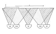
- FIG. 2 is an explanatory view showing a method of forming the organic EL layer 5 in the organic EL element 1 of the present embodiment, and is a view of each deposition source installed horizontally as viewed from the side.
- the material is deposited upward from each deposition source installed in this way. Therefore, by transporting the substrate 2 along the direction in which the respective vapor deposition sources are lined up (in the “x” direction in FIG. 2), the acceptor, the charge transporting material, The organic light-emitting material, the charge transporting material, and the donor can be deposited on the substrate 2 in this order. By using such an in-line type vapor deposition apparatus, it can produce more efficiently.
- each deposition source is not limited to the upward direction, and may be, for example, downward or horizontal. That is, the material may be deposited in any direction from top to bottom and left and right from the deposition source.
- each deposition source when each deposition source is installed horizontally, it is more preferable to deposit the material vertically downward or horizontally from the deposition source.
- the substrate 2 is moved along the material supply side to form the organic EL layer 5.
- the substrate 2 is moved along the material supply side to form the organic EL layer 5.
- it is used to separately coat each color in the production line. It is no longer necessary to keep the shadow mask suspended. Therefore, since it is possible to reduce the bending of the mask caused by the suspension, for example, when an EL element is manufactured over a large substrate, patterning can be performed using the mask. As a result, productivity can be improved and costs can be reduced.
- the manufacturing method of the organic EL element 1 is not limited to this,
- a crucible filled with an acceptor, an organic light emitting material, a donor, and a charge transporting material is connected to a planar evaporation source, and the crucible and the surface
- a vapor deposition apparatus provided with a valve for controlling the vapor of the organic material between the vapor deposition source may be used.
- the substrate is deposited on the upper side, the lower side, or the vertical direction of the planar vapor deposition source. Also in the film-forming method using such a vapor deposition apparatus, since the organic EL layer 5 is formed by conveying a board
- the electrodes constituting the organic EL element 1 may function as a pair like the anode 3 and the cathode 4.
- Each electrode may have a single-layer structure made of one electrode material or a laminated structure made of a plurality of electrode materials.
- the electrode material that can be used as the electrode of the organic EL element 1 is not particularly limited, and for example, a known electrode material can be used.
- an electrode material for example, an electrode material that can efficiently inject holes into the organic EL layer 5 and that has a work function of 4.5 or more is preferable as an anode material. On the other hand, an electrode material that can efficiently inject electrons and has a work function of 4.5 or less is preferable.
- Examples of electrode materials having a work function of 4.5 or more include metals such as gold (Au), platinum (Pt), and nickel (Ni), and oxides (ITO) composed of indium (In) and tin (Sn). ), An oxide of tin (Sn) (SnO 2 ), and an oxide (IZO) of indium (In) and zinc (Zn).
- metals such as gold (Au), platinum (Pt), and nickel (Ni), and oxides (ITO) composed of indium (In) and tin (Sn).
- IZO oxide of indium (In) and zinc (Zn).
- an electrode material having a work function of 4.5 or less for example, a metal such as lithium (Li), calcium (Ca), cerium (Ce), barium (Ba), aluminum (Al), or the like is contained. Including alloys such as Mg: Ag alloy and Li: Al alloy.
- an electrode material having the work function of 4.5 or more is used for the anode, and a work function is 4.5 or less for the cathode. It is necessary to use the electrode material.
- the acceptor region 6 of the organic EL layer 5 is doped with the acceptor and the donor region 8 is doped with the donor, so that the band structure is changed and the charge injection efficiency is improved. is doing. Therefore, an electrode material having a work function of 4.5 or less may be used for the anode 3, and an electrode material having a work function of 4.5 or more may be used for the cathode 4.
- the method for forming the electrode is not particularly limited, and can be formed by a known method such as an EB vapor deposition method, a sputtering method, an ion plating method, or a resistance heating vapor deposition method.
- the electrode formed by the above-described method can be patterned by a photolithography method or a laser peeling method, and further, a patterned electrode can be directly formed by combining with a shadow mask. Is also possible.
- the film thickness of each electrode is not particularly limited, but is preferably 50 nm or more.
- the film thickness is 50 nm or more, it is possible to prevent an increase in drive voltage caused by an increase in wiring resistance.
- the light emission obtained in the organic EL layer 5 may be extracted from one electrode side, that is, radiated outward.
- a transparent electrode as the electrode from which light emission is extracted.
- the transparent electrode material used for forming the transparent electrode is not particularly limited, but ITO or IZO is particularly preferable.
- the film thickness of the transparent electrode is preferably in the range of 50 to 500 nm, for example, and more preferably in the range of 100 to 300 nm.
- the film thickness is 50 nm or more, it is possible to prevent an increase in drive voltage caused by an increase in wiring resistance.
- the film thickness is 500 nm or less, it is possible to prevent a decrease in luminance without decreasing the light transmittance.
- a translucent electrode as the electrode from which light emission is extracted.
- an electrode material used for forming the semitransparent electrode for example, a metal semitransparent electrode alone may be used, or a metal semitransparent electrode alone and a transparent electrode material may be used in combination.
- a translucent electrode material it is more preferable to use silver from the viewpoint of reflectance and transmittance.
- the film thickness of the semitransparent electrode is preferably in the range of 5 to 30 nm, for example.
- the film thickness is 5 nm or more, it is possible to sufficiently reflect light and to obtain a sufficient interference effect.
- the film thickness is 30 nm or less, the light transmittance is not rapidly decreased, and the decrease in luminance and light emission efficiency can be prevented.
- an electrode material that does not transmit light is used as the cathode 4 (or anode 3) that is the other electrode.
- a black electrode such as tantalum or carbon
- a reflective metal electrode such as aluminum, silver, gold, an aluminum-lithium alloy, an aluminum-neodymium alloy, or an aluminum-silicon alloy may be used.
- a transparent electrode and the reflective metal electrode (reflective electrode) may be used in combination.
- FIG. 3 is a schematic view showing a configuration of an organic electroluminescence element according to the second embodiment of the present invention.
- the graph shown in FIG. 3 shows the concentration in the film thickness direction of the acceptor, donor, and both charge transporting materials contained in each layer of the organic EL element 10, and the layer structure and position of the organic EL element 10 correspond to each other. It shows. That is, in the graph of FIG. 3, the straight lines indicating the donor concentration and the charge transporting material concentration intersecting with the donor concentration are the donor concentration and the charge transporting material concentration in the charge transporting material region 16 and the donor region 17 described later.
- the straight line indicating the acceptor concentration and the concentration of both charge transport materials intersecting with the acceptor concentration indicates the acceptor concentration and the concentration of both charge transport materials in the acceptor region 13 and both charge transport material regions 14 described later.
- the organic EL element 10 includes an anode 12, a cathode 18, and an organic EL layer 19.
- the organic EL element 10 according to this embodiment has the same configuration as that of the first embodiment except that the configuration of the organic EL layer 19 is different from that of the first embodiment.
- the organic EL element 10 includes a charge transporting material region 14 that does not include an acceptor and an organic light emitting material between the acceptor region 13 and the light emitting region 15 of the organic EL layer 5. Further, between the donor region 17 and the light emitting region 15, the both charge transporting material region 16 not including the donor and the organic light emitting material is included.
- the holes transported from the acceptor region 13 are injected into the light emitting region 15 doped with the organic light emitting material, the holes are passed through the charge transporting material region 14 not including the acceptor and the organic light emitting material.
- the organic light emitting material and the acceptor are not in direct contact with each other, so that excitons generated in the organic light emitting material can be prevented from deactivating due to energy transfer to the acceptor. Therefore, high luminous efficiency can be realized effectively.
- the electrons transported from the donor region 17 are injected into the light emitting region 15 doped with the organic light emitting material, the electrons are passed through the charge transporting material region not including the donor and the organic light emitting material. Accordingly, since the organic light emitting material and the donor are not in direct contact with each other, excitons generated in the organic light emitting material can be prevented from deactivating due to energy transfer to the donor. Therefore, high luminous efficiency can be realized effectively.
- the film thicknesses of the charge transporting material regions 14 and 16 are not particularly limited, but are preferably in the range of 5 to 30 nm. If the film thicknesses of both charge transporting material regions 14 and 16 are within this range, holes and electrons can be easily injected and transported, so that high characteristics (for example, maximum luminance, high efficiency, long life and low driving) Voltage).
- both the charge transporting material regions 14 and 16 may be provided in both the acceptor region 13 and the donor region 17, or one of them may be provided.
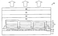
- FIG. 4 is a schematic diagram showing a configuration of an organic EL panel (display means) according to an embodiment of the present invention.
- the organic EL display device is an active matrix display device including the organic EL element 1 described above. Specifically, an organic EL panel 50 having a configuration in which a plurality of organic EL elements 1 are stacked on an active matrix substrate on which TFTs (thin film transistors) are formed is provided.
- TFTs thin film transistors
- the organic EL panel 50 includes a substrate 2, an anode 3, a cathode 4, an organic EL layer 5, a TFT circuit / wiring 51, an interlayer insulating film 52, a sealing film 53, and a resin film. 54, a sealing substrate 55, and a polarizing plate 56 are provided.
- the substrate 2 is provided with a TFT circuit / wiring 51 on its upper surface and functions as an active matrix substrate.
- the active matrix substrate has a plurality of scanning signal lines, data signal lines, and TFTs arranged at intersections between the scanning signal lines and the data signal lines on the substrate 2 serving as a base material. Further, two rows of the active matrix drive elements having such a configuration are made into one set, and the scanning signal lines are respectively arranged above and below.
- a switching TFT and a driving TFT are arranged for each pixel, and an interlayer insulating film 32 and a planarizing layer (not shown) are sequentially formed on the TFT.
- the driving TFT is electrically connected to the anode 3 through a contact hole formed in the planarization layer.
- a storage capacitor connected to the gate portion of the driving TFT is arranged in one pixel. This storage capacitor makes the gate potential of the driving TFT constant.
- the organic EL layers 5 be juxtaposed or laminated on the plurality of anodes 3 installed on the active matrix substrate.
- the organic EL layer 5 used in the organic EL panel is not particularly limited.
- a cathode 4 is provided on the organic EL layer 5 and functions as the organic EL element 1.
- the organic EL panel 50 according to this embodiment is driven by the voltage-driven digital gradation method, but is not limited to this, and may be driven by, for example, the current-driven analog gradation method. .
- the number of TFTs is not particularly limited. As described above, the organic EL element 1 may be driven using two TFTs, or the organic EL element 1 may be driven using two or more TFTs. Also good. When two or more TFTs are used, variations in TFTs can be prevented.
- a sealing substrate 55 is formed on the cathode 4 via a sealing film 53 or a resin film 54. It may be provided. Thereby, the organic EL element 1 can be protected from moisture or the like.
- the organic EL panel 50 may include a polarizing plate 56 on the sealing substrate 55. Thereby, the contrast of the organic EL panel 50 can be improved.
- substrate 2 As the substrate 2, for example, an inorganic material substrate including glass or quartz, a plastic substrate including polyethylene terephthalate, polycarbazole or polyimide, an insulating substrate such as a ceramic substrate including alumina, or the like, or aluminum (Al) or iron ( An insulating process is applied to the surface of a metal substrate containing Fe) etc. on a surface coated with an insulator containing silicon oxide (SiO 2 ), an organic insulating material, etc., or a metal substrate containing Al etc. by an anodic oxidation method or the like. And the like.
- the polysilicon TFT when the polysilicon TFT is formed by a low-temperature process in order to drive the organic EL element 1 in an active matrix, it is more preferable to use a substrate that does not melt at a temperature of 500 ° C. or less and does not cause distortion. preferable. Furthermore, when the polysilicon TFT is formed by a high temperature process, it is more preferable to use a substrate that does not melt at a temperature of 1,000 ° C. or less and does not cause distortion.
- the light emission obtained in the organic EL layer 5 is not in contact with the active matrix substrate, that is, from the cathode 4 side (the direction indicated by the arrow above the polarizing plate 56 in FIG. 4).
- the substrate material to be used is not particularly limited, but for example, when taking out the emitted light from the electrode in contact with the active matrix substrate, that is, from the anode 3 side, the substrate material is a transparent or translucent substrate. It is preferable to use a material.
- TFT circuit / wiring 51 A known TFT may be used as the TFT, and a metal-insulator-metal (MIM) diode may be used instead of the TFT.
- MIM metal-insulator-metal
- the TFT can be formed using a known material, structure, and formation method.
- amorphous silicon amorphous silicon
- polycrystalline silicon polysilicon
- microcrystalline silicon inorganic semiconductor materials such as cadmium selenide, or polythiophene derivatives, thiophene oligomers
- inorganic semiconductor materials such as cadmium selenide, or polythiophene derivatives, thiophene oligomers
- organic semiconductor materials such as poly (p-ferylene vinylene) derivatives, naphthacene, and pentacene.
- TFT structure include a staggered type, an inverted staggered type, a top gate type, and a coplanar type.
- a method for forming an active layer constituting a TFT As a method for forming an active layer constituting a TFT, a method of ion doping impurities into amorphous silicon formed by plasma induced chemical vapor deposition (PECVD), or low pressure chemical vapor deposition using silane (SiH 4 ) gas.
- PECVD plasma induced chemical vapor deposition
- SiH 4 silane
- Amorphous silicon is formed by (LPCVD) method, and amorphous silicon is crystallized by solid phase growth method to obtain polysilicon, followed by ion doping by ion implantation method, LPCVD method using Si 2 H 6 gas or SiH
- Amorphous silicon is formed by PECVD using 4 gases, annealed by a laser such as an excimer laser, and amorphous silicon is crystallized to obtain polysilicon, followed by ion doping (low temperature process), LPCVD or PECVD.
- Poly by law A recon layer is formed, a gate insulating film is formed by thermal oxidation at 1,000 ° C. or higher, an n + polysilicon gate electrode is formed thereon, and then ion doping (high temperature process) is performed. Examples thereof include a method for forming a semiconductor material by an inkjet method and the like, and a method for obtaining a single crystal film of an organic semiconductor material.
- the gate insulating film of the TFT can be formed using a known material. Examples thereof include SiO 2 formed by PECVD, LPCVD, etc., or SiO 2 obtained by thermally oxidizing a polysilicon film.
- the signal electrode line, the scanning electrode line, the common electrode line, the first drive electrode, and the second drive electrode of the TFT used in the organic EL panel 50 according to the present embodiment can be formed using known materials. Examples thereof include tantalum (Ta), aluminum (Al), and copper (Cu).
- the TFT of the organic EL panel according to this embodiment can be formed with the above-described configuration, but is not limited to these materials, structures, and formation methods.
- Interlayer insulating film 52 A known material may be used for the interlayer insulating film 52, for example, inorganic such as silicon oxide (SiO 2 ), silicon nitride (SiN or Si 2 N 4 ), tantalum oxide (TaO or Ta 2 O 5 ), etc. Examples thereof include organic materials such as materials, acrylic resins, and resist materials.
- Examples of the method for forming the interlayer insulating film 52 include a dry process such as a chemical vapor deposition (CVD) method and a vacuum deposition method, and a wet process such as a spin coating method. Moreover, it can also pattern by the photolithographic method etc. as needed.
- CVD chemical vapor deposition
- vacuum deposition method a vacuum deposition method
- wet process such as a spin coating method.
- it can also pattern by the photolithographic method etc. as needed.
- the light emission obtained in the organic EL layer 5 is taken out from the side not in contact with the active matrix substrate, that is, from the cathode 4 side, it is preferable to use a light-shielding insulating film having light-shielding properties. Thereby, even if external light is incident on the TFT formed on the substrate, it is possible to prevent the TFT characteristics from changing.
- the light-shielding interlayer insulating film examples include a material in which a pigment or dye such as phthalocyanine or quinaclone is dispersed in a polymer resin such as polyimide, a color resist, a black matrix material, and an inorganic insulating material such as NixZnyFe 2 O 4 . Note that any of these insulating films or light-shielding insulating films may be used as the interlayer insulating film, or a combination thereof may be used.
- the light-shielding interlayer insulating film of the organic EL panel according to this embodiment can be formed with the above-described configuration, but is not limited to these materials, structures, and formation methods.
- a planarization film may be provided over the insulating film 52.
- the planarizing film can be formed using a known material, and examples thereof include inorganic materials such as silicon oxide, silicon nitride, and tantalum oxide, and organic materials such as polyimide, acrylic resin, and resist material.
- planarizing film examples include dry processes such as CVD and vacuum deposition, and wet processes such as spin coating, but the present invention is not limited to these materials and forming methods. Further, the planarizing film may have a single layer structure or a multilayer structure.
- Organic EL element 1 The organic EL panel 50 according to the present embodiment only needs to include the organic EL element 1 including the single-layer organic EL layer 5. However, it is not limited to the configuration of the organic EL element 1 described above. For example, an insulating edge cover for preventing leakage is provided at the edge portion of the electrode in contact with the active matrix substrate. In the case where the organic EL element 1 is manufactured by a wet process, an insulating partition layer for holding the applied coating liquid may be provided.
- the organic EL panel 50 of the present invention may be provided with a polarizing plate 56 on the side from which the light emission obtained in the organic EL layer 5 is extracted.
- the polarizing plate 56 is not particularly limited, but for example, a combination of a conventional linear polarizing plate and a ⁇ / 4 plate is more preferable. By providing the polarizing plate 56, the contrast of the organic EL panel 50 can be improved.
- the organic EL panel 50 preferably has a sealing structure including the sealing film 53 or the sealing substrate 55.
- a sealing structure the structure which combined the sealing film 53 and the sealing substrate 55, for example may be sufficient, and the structure using only the sealing film 53 or the sealing substrate 55 may be sufficient.
- sealing film 53 examples include an inorganic film or a resin film
- examples of the sealing substrate 55 include a glass substrate.
- the formation method of the sealing film 53 and the sealing substrate 55 is not particularly limited, and can be formed by a known sealing material and sealing method.
- a forming method for example, a method of sealing an inert gas such as nitrogen gas or argon gas with glass or metal, or a method of mixing a hygroscopic agent such as barium oxide in the sealed inert gas Is mentioned.
- the sealing film 53 may be formed by applying or bonding a resin on the electrode by using, for example, a spin coating method, ODF (One Drop Drop Fill), or a laminating method. it can.
- the sealing structure on the electrode it is possible to prevent the entry of oxygen or moisture into the organic EL element 1 from the outside, and the life of the organic EL element 1 is improved.
- the material or forming method used for the sealing film 53 or the sealing substrate 55 is not limited to this.
- this invention is not limited to the organic EL display apparatus mentioned above,
- the organic EL lighting apparatus provided with the organic EL element which concerns on this invention is also contained in the scope of the present invention.
- Example 1 Evaluation of electrical characteristics of organic electroluminescence device according to the present invention
- an organic EL element was produced by the following method, and electrical characteristics were evaluated.
- a transparent substrate having a surface resistance of 10 ⁇ / ⁇ and a 50 mm square indium-tin oxide (ITO) formed on the surface was used, and ITO serving as an anode was patterned into a 2 mm wide stripe.
- the substrate was washed with water, subjected to pure water ultrasonic cleaning for 10 minutes, acetone ultrasonic cleaning for 10 minutes, isopropyl alcohol vapor cleaning for 5 minutes, and dried at 100 ° C. for 1 hour. Thereafter, the substrate was fixed to a substrate holder in a resistance heating deposition apparatus, the pressure was reduced to a vacuum of 1 ⁇ 10 -4 Pa.
- a dual charge transporting light emitting layer (organic EL layer) was formed to a thickness of 100 nm on the substrate.
- CZBDF bis (carbazoline) benzodifuran
- TCNQF 4 tetrafluorotetracyanoquinodimethane
- III tris (2-phenylpyridine) iridium (III) is used as the organic light emitting material.
- Ir (ppy) 3 ) tetrathiafulvalene (TTF) was used as a donor.
- the acceptor was doped by co-evaporation in a region extending from the anode to a position of 40 nm so that the doping concentration decreased linearly from the anode side. Specifically, doping was performed so that the doping concentration of TCNQF 4 was 15 wt% at the maximum on the anode side, and the doping concentration was 0 wt% at a position 40 nm from the anode.
- the donor was doped by co-evaporation in a region extending from the cathode to a position of 40 nm so that the doping concentration decreased linearly from the cathode side.
- doping was performed so that the doping concentration of TTF was 10 wt% at the maximum on the cathode side, and the doping concentration was 0 wt% at a position 40 nm from the cathode.
- Ir (ppy) 3 was doped into the region (20 nm) located at the center of both charge transporting light emitting layers by co-evaporation so that the doping concentration was 6 wt%.
- silver (Ag) was deposited on both charge transporting light emitting layers (deposition rate: 2 nm / second) to form a cathode having a thickness of 100 nm.
- a glass substrate was bonded to the substrate via a UV (ultraviolet) curable resin, and the resin was cured by irradiating 6,000 mJ of UV light using a UV lamp, followed by sealing.
- an organic EL device comprising an anode, a charge transporting light emitting layer and a cathode, that is, a single organic layer was obtained.
- the luminous efficiency was 33 cd / A and the luminance was 14,000 cd / m 2 .
- the lifetime from when the luminance was adjusted to 1,000 cd / m 2 to when the luminance was reduced by half was 20,000 hours.
- Comparative Example 1 Organic electroluminescent device having multilayer structure
- an organic EL element composed of six organic layers was produced by the following method.
- a transparent substrate having a surface resistance of 10 ⁇ / ⁇ and a 50 mm square indium-tin oxide (ITO) formed on the surface was used, and ITO serving as an anode was patterned into a 2 mm wide stripe.
- the substrate was washed with water, subjected to pure water ultrasonic cleaning for 10 minutes, acetone ultrasonic cleaning for 10 minutes, isopropyl alcohol vapor cleaning for 5 minutes, and dried at 100 ° C. for 1 hour. Thereafter, the substrate was fixed to a substrate holder in a resistance heating vapor deposition apparatus, and the pressure was reduced to a vacuum of 1 ⁇ 10 ⁇ 4 Pa or less.
- a hole injection layer having a film thickness of 20 nm was formed by resistance heating vapor deposition using LGC101 (LG Chem, LTD.) As a hole injection material.
- NPB N, N′-di-1-naphthyl-N, N′-diphenyl-1,1′biphenyl-1,1′-biphenyl-4,4′-diamine
- the film thickness is formed by resistance heating evaporation using bis (carbazoline) benzodifuran (CZBDF) as the host material and tris (2-phenylpyridine) iridium (III) (Ir (ppy) 3 ) as the organic light emitting material. A 30 nm light emitting layer was formed. This time was 8 wt% doping Ir (ppy) 3 by coevaporation to the host material.
- a hole blocking layer having a thickness of 10 nm was formed by resistance heating vapor deposition using 2,9-dimethyl-4,7-diphenyl-1,10-phenanthroline (BCP) as a hole blocking material.
- BCP 2,9-dimethyl-4,7-diphenyl-1,10-phenanthroline
- an electron transport layer having a thickness of 20 nm was formed by resistance heating vapor deposition using an aluminum quinolinol complex (Alq3) as an electron transport material.
- an electron injection layer having a thickness of 1 nm was formed by resistance heating vapor deposition using lithium fluoride (LiF) as an electron injection material.
- silver (Ag) was deposited on the electron injection layer (deposition rate: 2 nm / second) to form a cathode having a thickness of 100 nm.
- an organic EL device comprising an anode, a hole injection layer, a hole transport layer, a light emitting layer, a hole blocking layer, an electron transport layer, an electron injection layer and a cathode, that is, a multilayer organic layer was obtained.
- the luminous efficiency was 32 cd / A and the luminance was 12,000 cd / m 2 .
- the lifetime from when the luminance was adjusted to 1,000 cd / m 2 to when the luminance was reduced by half was 16,000 hours.
- Comparative Example 2 Organic electroluminescent device having a single layer structure
- an organic EL element composed of a single organic layer was produced by the same method as in Example 1.
- the region on the anode side 40 nm is doped with TCNQF 4 so that the doping concentration is constant at 15 wt%, and the region on the cathode side 40 nm.
- TTF doped with TTF so that the doping concentration was constant at 10 wt%.
- a region (20 nm) located at the center of both charge transporting light emitting layers was doped with Ir (ppy) 3 so that the doping concentration was 6 wt%.
- the electrical characteristics of the obtained organic EL device of Comparative Example 2 were measured by the same method as in Example 1. As a result, the luminous efficiency was 20 cd / A and the luminance was 8,000 cd / m 2 . As a result of the brightness from the time of adjusting the luminance 1,000 cd / m 2 was measured lifetime until half, was 6,000 hours.
- Comparative Example 2 the region doped with a high concentration of the acceptor and the region doped with the organic light emitting material are in contact with each other, so that the holes propagating through the acceptor are doped with the organic light emitting material. It has been found that it cannot efficiently propagate to both charge transport materials in the region. In addition, since the region doped with a high concentration donor and the region doped with the organic light emitting material are in contact with each other, the electrons propagating through the donor are both charge transport materials in the region doped with the organic light emitting material. It was found that it cannot propagate efficiently.
- the organic EL element of Example 1 is compared with the organic EL elements of Comparative Examples 1 and 2, the luminous efficiency is greatly improved from 20 cd / A to 33 cd / A of Comparative Example 2, and the comparison is a multilayer stacked element. It turned out that the characteristic equivalent to 32 cd / A of Example 1 is acquired. The luminance also significantly improved from 8,000 cd / m 2 in Comparative Example 2 to 14,000cd / m 2, characteristics equivalent to those of 12,000cd / m 2 of Comparative Example 1 is obtained. Further, the luminance half-life was also greatly improved from 6,000 hours in Comparative Example 2 to 20,000 hours, and it was found that the same characteristics as 16,000 hours in Comparative Example 1 were obtained.
- the acceptor has a concentration gradient so that the HOMO level in the region where holes propagate is lowest on the side in contact with the anode, and the organic light emitting material is doped. It was found that the holes injected from the anode can be efficiently transported to the region where the organic light-emitting material is doped because the HOMO level of the both charge transporting materials almost coincides with the HOMO level of the both regions. .
- the LUMO level in the region where electrons are propagated is highest on the side in contact with the cathode, and on the region side where the organic light emitting material is doped, Since it almost coincides with the LUMO level, it was found that electrons injected from the cathode can be efficiently transported to the region where the organic light emitting material is doped.
- Example 2 an organic EL element was produced by the same method as in Example 1. However, in Example 1, when the acceptor and the donor were doped, a concentration gradient was linearly added, whereas in Example 2, the concentration gradient was exponentially added.
- the electrical characteristics of the obtained organic EL device of Example 2 were measured by the same method as in Example 1. As a result, the luminous efficiency was 45 cd / A and the luminance was 22,000 cd / m 2 . The lifetime from when the luminance was adjusted to 1,000 cd / m 2 to when the luminance was reduced to half was 24,000 hours.
- Example 1 when the organic EL elements of Example 1 and Example 2 were compared, the luminous efficiency was improved from 33 cd / A in Example 1 to 45 cd / A, and the luminance was also increased from 14,000 cd / m 2 in Example 1. It improved to 22,000 cd / m 2 . Further, the luminance half life was improved from 20,000 hours in Example 1 to 24,000 hours.
- the concentration gradient of acceptor and donor is changed from a linear gradient to an exponential gradient, so that holes and electrons are more efficiently propagated to both charge transport materials in the light emitting region. I found out that I could do it. Further, it has been found that it is possible to more effectively prevent a decrease in light emission efficiency due to energy transfer of excitation energy from the light emitting material to the acceptor and donor.
- Example 3 In Example 3, CZBDF as a charge transporting material, TCNQF 4 as an acceptor, Ir (ppy) 3 as an organic light emitting material, and TTF as a donor were used, and both charges having a thickness of 120 nm were formed in the same manner as in Example 1. A transporting light emitting layer was formed.
- Example 3 the exponential function is set so that the maximum doping concentration of TCNQF 4 is 15 wt% on the anode side and the doping concentration is 0 wt% at the position of 40 nm from the anode in the region reaching the position of 40 nm from the anode. In order to reduce the doping concentration, it was doped by co-evaporation.
- the doping concentration is exponentially so that the maximum TTF doping concentration is 10 wt% on the cathode side and the doping concentration is 0 wt% at the position of 40 nm from the cathode. It was doped by co-evaporation to decrease. Furthermore, the region (20 nm) located at the center of the both charge transporting light emitting layer has Ir (through the region composed only of the acceptor, donor, and both charge transporting materials not doped with the organic light emitting material, Ir ( ppy) 3 was doped by co-evaporation so that the doping concentration was 6 wt%.
- the electrical characteristics of the obtained organic EL device of Example 3 were measured by the same method as in Example 1. As a result, the light emission efficiency was 50 cd / A and the luminance was 25,000 cd / m 2 . The lifetime from when the luminance was adjusted to 1,000 cd / m 2 to when the luminance was reduced by half was 30,000 hours.
- Example 2 when the organic EL elements of Example 2 and Example 3 were compared, the luminous efficiency was improved from 45 cd / A of Example 2 to 50 cd / A, and the luminance was from 22,000 cd / m 2 of Example 2. Improved to 25,000 cd / m 2 . Further, the luminance half life was improved from 24,000 hours in Example 2 to 30,000 hours.
- Example 4 Production of organic EL display device
- an organic EL display device was produced by the following method.
- an amorphous silicon semiconductor film was formed on a glass substrate by PECVD.
- a polycrystalline silicon semiconductor film was formed by subjecting this substrate to a crystallization treatment.
- the polycrystalline silicon semiconductor film was patterned into a plurality of islands using a photolithography method. Subsequently, a gate insulating film and a gate electrode layer were sequentially formed on the patterned polycrystalline silicon semiconductor layer, and patterned using a photolithography method.
- source and drain regions were formed by doping the patterned polycrystalline silicon semiconductor film with an impurity element such as phosphorus, and a TFT element was fabricated, and then a planarizing film was formed.
- the planarizing film was formed by sequentially laminating a silicon nitride film formed by PECVD and an acrylic resin layer using a spin coater.
- a silicon nitride film is first formed, and then the silicon nitride film and the gate insulating film are etched together to form a contact hole that leads to the source and / or drain region. Formed. Thereafter, an acrylic resin layer was formed, and a contact hole communicating with the drain region was formed at the same position as the contact hole of the drain region drilled in the gate insulating film and the silicon nitride film. Thus, an active matrix substrate was obtained.
- the function as a planarizing film is realized by an acrylic resin layer.
- the storage capacitor for making the gate potential of the TFT constant is formed by interposing an insulating film such as an interlayer insulating film between the drain of the switching TFT and the source of the driving TFT.
- a contact hole is provided through the planarization layer to electrically connect the driving TFT and the first electrode (anode or cathode) of the organic EL element of red, green, and blue pixels. It was.
- the first electrode is formed by first forming a 100 nm film using Ag (silver), and subsequently forming a 20 nm film using ITO (indium oxide-tin oxide). At this time, the area of the first electrode was set to 300 ⁇ m ⁇ 300 ⁇ m.
- SiO 2 of the first electrode was laminated by sputtering, and patterned to cover the edge portion of the first electrode by conventional photolithography.
- an active matrix substrate was obtained by covering the four sides with SiO 2 by 10 ⁇ m from the edge of the first electrode.
- This active matrix substrate was cleaned.
- the active matrix substrate was cleaned by ultrasonic cleaning using acetone and IPA for 10 minutes, and then UV-ozone cleaning for 30 minutes.
- the doping concentration is linearly decreased so that the maximum doping concentration of TCNQF 4 is 20 wt% on the anode side and the doping concentration is 0 wt% at the position 40 nm from the anode. As such, it was doped by co-evaporation.
- the doping concentration decreases linearly so that the maximum doping concentration of Cs is 10 wt% on the cathode side and the doping concentration is 0 wt% at the position 40 nm from the cathode. It was doped by co-evaporation.
- the region (20 nm) located at the center of the both charge transporting light emitting layer has a region composed of only the acceptor, donor, and both charge transporting materials not doped with the organic light emitting material (10 nm each). Then, FIrpic was doped by co-evaporation so that the doping concentration was 6 wt%.
- a green light emitting pixel was formed on the surface of the first electrode by vapor deposition using a shadow mask.
- a dual charge transporting light emitting layer having a film thickness of 160 nm was formed using DPABDF as the charge transporting material, TCNQF 4 as the acceptor, Cs as the donor, and Ir (ppy) 3 as the organic green light emitting material.
- the doping concentration decreases linearly so that the maximum doping concentration of TCNQF 4 is 20 wt% on the anode side and the doping concentration is 0 wt% at the position 80 nm from the anode. As such, it was doped by co-evaporation.
- the doping concentration decreases linearly so that the maximum doping concentration of Cs is 10 wt% on the cathode side and the doping concentration is 0 wt% at the position 40 nm from the cathode. It was doped by co-evaporation.
- the region (20 nm) located at the center of the both charge transporting light emitting layer has a region (20 nm each) composed only of the acceptor, donor, and both charge transporting materials not doped with the organic light emitting material.
- Ir (ppy) 3 was doped by co-evaporation so that the doping concentration was 6 wt%.
- red light emitting pixels were formed on the surface of the first electrode by vapor deposition using a shadow mask.
- DPABDF charge transport material
- TCNQF 4 acceptor
- Cs the donor
- T1 2.0 eV (Ir (piq) 3 ) as the organic red light emitting material
- the doping concentration of the TCNQF 4 is 20 wt% at the maximum on the anode side, and the doping concentration is linearly decreased so that the doping concentration is 0 wt% at the position of 140 nm from the anode. As such, it was doped by co-evaporation.
- the doping concentration decreases linearly so that the maximum doping concentration of Cs is 10 wt% on the cathode side and the doping concentration is 0 wt% at the position 40 nm from the cathode. It was doped by co-evaporation.
- the region (20 nm) located at the center of the both charge transporting light emitting layer has a region (20 nm each) composed only of the acceptor, donor, and both charge transporting materials not doped with the organic light emitting material.
- Ir (piq) 3 was doped by co-evaporation so that the doping concentration was 6 wt%.
- a second electrode (electrode paired with the first electrode) was formed.
- the substrate on which the pixels were formed was fixed in a metal deposition chamber.
- the shadow mask for forming the second electrode and the substrate were aligned, and silver was formed in a desired pattern (thickness: 10 nm) on the surface of the organic EL layer by vacuum deposition. Thereby, a semitransparent second electrode was formed.
- an inorganic protective layer made of 2 ⁇ m of SiO 2 is formed on the semi-transparent second electrode by plasma CVD, and an inorganic protective layer is formed only on the part where the wiring is taken out from the display (FPC connection part) using a shadow mask. Patterning was formed so as not to occur.
- the sealing glass in which a UV curable resin adhesive is applied to the sealing glass with a dispenser, is bonded to the substrate in a dry air environment (water content: ⁇ 80 ° C.), irradiated with curing UV light, and cured. did.
- a polarizing plate was bonded to a substrate positioned in a direction in which light generated in the organic EL layer was extracted to the outside, and an organic EL panel was obtained.
- an organic EL display device was obtained by mounting an external drive circuit or the like on the organic EL panel.
- Example 5 an organic EL element was produced by the same method as in Example 1. However, in Example 1, when the acceptor and donor were doped, a concentration gradient was linearly formed, whereas in Example 5, the concentration decreased from the electrode in proportion to the square of the distance from the electrode. A concentration gradient was added.
- the electrical characteristics of the obtained organic EL device of Example 5 were measured by the same method as in Example 1. As a result, the luminous efficiency was 40 cd / A and the luminance was 21,000 cd / m 2 . The lifetime from when the luminance was adjusted to 1,000 cd / m 2 to when the luminance was reduced by half was 22,000 hours.
- Example 5 when comparing the organic EL device of Example 1 and Example 5, the luminous efficiency is improved from 33cd / A of Example 1 to 40 cd / A, the luminance from 14,000cd / m 2 of Example 1 It improved to 21,000 cd / m 2 . Further, the luminance half life was improved from 20,000 hours in Example 1 to 22,000 hours.
- acceptor and donor concentration gradients are made more efficient by making the concentration gradient from the linear gradient to a concentration decreasing from the electrode in proportion to the square of the distance from the electrode. It was found that electrons can propagate to both charge transport materials in the light emitting region. In addition, it has been found that a decrease in light emission efficiency accompanying energy transfer of excitation energy from the light emitting material to the acceptor and donor can be more effectively prevented.
- Example 6 In Example 6, an organic EL element was produced by the same method as in Example 1. However, in Example 1, when the acceptor and the donor were doped, a concentration gradient was linearly formed, whereas in Example 6, the concentration decreased from the electrode in proportion to the cube of the distance from the electrode. A concentration gradient was added.
- the electrical characteristics of the obtained organic EL device of Example 6 were measured by the same method as in Example 1. As a result, the light emission efficiency was 41 cd / A and the luminance was 22,000 cd / m 2 . The lifetime from when the luminance was adjusted to 1,000 cd / m 2 to when the luminance was reduced by half was 22,000 hours.
- Example 1 when the organic EL elements of Example 1 and Example 6 were compared, the luminous efficiency was improved from 33 cd / A of Example 1 to 41 cd / A, and the luminance was from 14,000 cd / m 2 of Example 1. It improved to 22,000 cd / m 2 . Further, the luminance half life was improved from 20,000 hours in Example 1 to 22,000 hours.
- acceptor and donor concentration gradients are made more efficient by making the gradient from a linear gradient to a concentration decreasing from the electrode in proportion to the cube of the distance from the electrode. It was found that electrons can propagate to both charge transport materials in the light emitting region. In addition, it has been found that a decrease in light emission efficiency accompanying energy transfer of excitation energy from the light emitting material to the acceptor and donor can be more effectively prevented.
- Example 7 In Example 7, an organic EL element was produced by the same method as in Example 1. However, in Example 1, when the acceptor and donor were doped, a concentration gradient was linearly formed, whereas in Example 7, the concentration decreased from the electrode in proportion to the fourth power of the distance from the electrode. A concentration gradient was added.
- the electrical characteristics of the obtained organic EL device of Example 7 were measured by the same method as in Example 1. As a result, the light emission efficiency was 42 cd / A and the luminance was 22,000 cd / m 2 . The lifetime from when the luminance was adjusted to 1,000 cd / m 2 to when the luminance was reduced by half was 22,000 hours.
- Example 1 when the organic EL elements of Example 1 and Example 7 were compared, the luminous efficiency was improved from 33 cd / A of Example 1 to 42 cd / A, and the luminance was 14,000 cd / m 2 of Example 1. It improved to 22,000 cd / m 2 . Further, the luminance half life was improved from 20,000 hours in Example 1 to 22,000 hours.
- acceptor and donor concentration gradients are made more efficient by making the gradient from the linear gradient to a concentration decreasing from the electrode in proportion to the fourth power of the distance from the electrode. It was found that electrons can propagate to both charge transport materials in the light emitting region. In addition, it has been found that a decrease in light emission efficiency accompanying energy transfer of excitation energy from the light emitting material to the acceptor and donor can be more effectively prevented.
- Example 8 an organic EL element was produced by the same method as in Example 1. However, in Example 1, when the acceptor and the donor were doped, a concentration gradient was linearly formed, whereas in Example 7, the concentration decreased from the electrode in proportion to the fifth power of the distance from the electrode. A concentration gradient was added.
- the electrical characteristics of the obtained organic EL device of Example 8 were measured by the same method as in Example 1. As a result, the luminous efficiency was 43 cd / A and the luminance was 22,000 cd / m 2 . The lifetime from when the luminance was adjusted to 1,000 cd / m 2 to when the luminance was reduced by half was 22,000 hours.
- Example 1 when the organic EL elements of Example 1 and Example 8 were compared, the luminous efficiency was improved from 33 cd / A of Example 1 to 43 cd / A, and the luminance was from 14,000 cd / m 2 of Example 1. It improved to 22,000 cd / m 2 . Further, the luminance half life was improved from 20,000 hours in Example 1 to 22,000 hours.
- acceptor and donor concentration gradients are made more efficient by making the concentration gradient from the linear gradient to a gradient such that the concentration decreases from the electrode in proportion to the fifth power of the distance from the electrode. It was found that electrons can propagate to both charge transport materials in the light emitting region. In addition, it has been found that a decrease in light emission efficiency accompanying energy transfer of excitation energy from the light emitting material to the acceptor and donor can be more effectively prevented.
- Example 9 an organic EL element was produced by the same method as in Example 2. However, in Example 9, when the region (20 nm) located at the center of the both charge transporting light emitting layer is doped with Ir (ppy) 3 by co-evaporation so that the doping concentration becomes 6 wt%, both charge transporting properties are obtained. A concentration gradient was provided so that the maximum doping amount was 6 wt% at the center of the light emitting layer (position 50 nm from the anode), and the doping concentration decreased exponentially toward the anode or cathode, respectively.
- the electrical characteristics of the obtained organic EL device of Example 9 were measured by the same method as in Example 1. As a result, the luminous efficiency was 50 cd / A and the luminance was 24,000 cd / m 2 . The lifetime from when the luminance was adjusted to 1,000 cd / m 2 to when the luminance was reduced by half was 35,000 hours.
- Example 9 when the organic EL elements of Example 2 and Example 9 were compared, the luminous efficiency was improved from 45 cd / A of Example 2 to 50 cd / A, and the luminance was from 22,000 cd / m 2 of Example 2. It improved to 24,000 cd / m 2 . Further, the luminance half-life was improved from 24,000 hours in Example 2 to 35,000 hours.
- Example 10 an organic EL element was produced by the same method as in Example 2. However, in Example 10, when the region (20 nm) located at the center of the both charge transporting light emitting layer is doped with Ir (ppy) 3 by co-evaporation so that the doping concentration is 6 wt%, both charge transporting properties are obtained. A concentration gradient was applied so that the maximum doping amount was 6 wt% at the center of the light emitting layer (position 50 nm from the anode), and the doping concentration decreased in proportion to the square of the distance toward the anode or cathode, respectively.
- the electrical characteristics of the obtained organic EL device of Example 10 were measured by the same method as in Example 1. As a result, the light emission efficiency was 52 cd / A and the luminance was 24,000 cd / m 2 . The lifetime from when the luminance was adjusted to 1,000 cd / m 2 to when the luminance was reduced by half was 37,000 hours.
- Example 2 when the organic EL elements of Example 2 and Example 10 were compared, the luminous efficiency was improved from 45 cd / A of Example 2 to 52 cd / A, and the luminance was also from 22,000 cd / m 2 of Example 2. It improved to 24,000 cd / m 2 . Further, the luminance half life was improved from 24,000 hours in Example 2 to 37,000 hours.
- the concentration gradient of the light emitting material is made such that the doping concentration decreases in proportion to the square of the distance toward the anode or the cathode, respectively, so that holes and electrons are more efficiently emitted in the light emitting region. It was found that it can propagate to both charge transport materials. In addition, it has been found that a decrease in light emission efficiency accompanying energy transfer of excitation energy from the light emitting material to the acceptor and donor can be more effectively prevented.
- Example 11 an organic EL element was produced by the same method as in Example 2. However, in Example 11, when a region (20 nm) located at the center of the both charge transporting light emitting layer is doped by Ir (ppy) 3 so that the doping concentration is 6 wt%, both charge transport properties are obtained. A concentration gradient was provided so that the maximum doping amount was 6 wt% at the center of the light emitting layer (position 50 nm from the anode), and the doping concentration decreased in proportion to the cube of the distance toward the anode or cathode, respectively.
- the electrical characteristics of the obtained organic EL device of Example 11 were measured by the same method as in Example 1. As a result, the light emission efficiency was 53 cd / A and the luminance was 24,000 cd / m 2 . The lifetime from when the luminance was adjusted to 1,000 cd / m 2 to when the luminance was reduced by half was 38,000 hours.
- Example 2 when the organic EL elements of Example 2 and Example 11 were compared, the luminous efficiency was improved from 45 cd / A of Example 2 to 53 cd / A, and the luminance was also from 22,000 cd / m 2 of Example 2. It improved to 24,000 cd / m 2 . Further, the luminance half life was improved from 24,000 hours in Example 2 to 38,000 hours.
- the concentration gradient of the light emitting material is made such that the doping concentration decreases in proportion to the cube of the distance toward the anode or the cathode, respectively, so that holes and electrons are more efficiently emitted into the light emitting region. It was found that it can propagate to both charge transport materials. In addition, it has been found that a decrease in light emission efficiency accompanying energy transfer of excitation energy from the light emitting material to the acceptor and donor can be more effectively prevented.
- Example 12 an organic EL element was produced by the same method as in Example 2. However, in Example 12, when the region (20 nm) located at the center of the both charge transporting light emitting layer is doped with Ir (ppy) 3 so as to have a doping concentration of 6 wt%, both charge transporting properties are achieved. A concentration gradient was applied so that the maximum doping amount was 6 wt% at the center of the light emitting layer (position 50 nm from the anode), and the doping concentration decreased in proportion to the fourth power of the distance toward the anode or cathode, respectively.
- the electrical characteristics of the obtained organic EL device of Example 12 were measured by the same method as in Example 1. As a result, the luminous efficiency was 53 cd / A and the luminance was 24,000 cd / m 2 . The lifetime from when the luminance was adjusted to 1,000 cd / m 2 to when the luminance was reduced by half was 33,000 hours.
- Example 2 when the organic EL elements of Example 2 and Example 12 were compared, the luminous efficiency was improved from 45 cd / A of Example 2 to 53 cd / A, and the luminance was also from 22,000 cd / m 2 of Example 2. It improved to 24,000 cd / m 2 . Further, the luminance half life was improved from 24,000 hours in Example 2 to 33,000 hours.
- the concentration gradient of the luminescent material is made such that the doping concentration decreases in proportion to the fourth power of the distance toward the anode or the cathode, respectively, so that holes and electrons are more efficiently emitted in the light emitting region. It was found that it can propagate to both charge transport materials. In addition, it has been found that a decrease in light emission efficiency accompanying energy transfer of excitation energy from the light emitting material to the acceptor and donor can be more effectively prevented.
- Example 13 In Example 13, an organic EL element was produced by the same method as in Example 2. However, in Example 13, when doping Ir (ppy) 3 by co-evaporation so that the doping concentration is 6 wt% in the region (20 nm) located at the center of the both charge transporting light emitting layer, both charge transporting properties are achieved. A concentration gradient was set so that the maximum doping amount was 6 wt% at the center of the light emitting layer (position 50 nm from the anode), and the doping concentration decreased in proportion to the fifth power of the distance toward the anode or cathode, respectively.
- the electrical characteristics of the obtained organic EL device of Example 13 were measured by the same method as in Example 1. As a result, the light emission efficiency was 54 cd / A and the luminance was 24,000 cd / m 2 . The lifetime from when the luminance was adjusted to 1,000 cd / m 2 to when the luminance was reduced by half was 38,000 hours.
- Example 2 when the organic EL elements of Example 2 and Example 13 were compared, the luminous efficiency was improved from 45 cd / A of Example 2 to 54 cd / A, and the luminance was also from 22,000 cd / m 2 of Example 2. It improved to 24,000 cd / m 2 . Further, the luminance half life was improved from 24,000 hours in Example 2 to 38,000 hours.
- the concentration of the organic light emitting material increases from the side facing the first region and the second region toward the center. It is preferable that the gradient is given.
- the concentration of the organic light emitting material is low in the interface region between the first region and the third region. Therefore, the holes propagating through the acceptor can be efficiently propagated to the charge transporting material in the interface region, and finally the holes are completely propagated in the charge transporting material in the third region. be able to.
- the concentration of the organic light emitting material is low in the interface region between the second region and the third region. Therefore, the electrons propagating through the donor can be efficiently propagated in the charge transporting material in the interface region, and finally the electrons are completely propagated in the charge transporting material in the third region. Can do.
- the organic electroluminescence element according to the present invention includes a charge transport material region that does not contain the acceptor and the organic light emitting material between the first region and the third region. preferable.
- both charge transport property which does not contain an acceptor and an organic light emitting material is included. Through the material region.
- the organic electroluminescence device may include a charge transport material region that does not contain the donor and the organic light emitting material between the second region and the third region. preferable.
- both charge transport material which does not contain a donor and an organic light emitting material Through the area.
- the film thickness of the both charge transporting material regions is preferably 5 to 30 nm. This facilitates the injection and transport of holes and electrons, so that high characteristics (for example, maximum luminance, high efficiency, long life, low driving voltage, etc.) can be obtained.
- the acceptor concentration gradient in the first region and the donor concentration gradient in the second region are exponentially applied.
- the concentration gradient of the acceptor in the first region is proportional to the nth power (n ⁇ 1) of the distance from the anode, and the third gradient from the anode side.
- the concentration gradient of the donor in the second region is proportional to the nth power of the distance from the cathode (n ⁇ 1) from the cathode side. It is preferable that the concentration decreases toward the third region.
- the supply means are installed horizontally, and an acceptor, an organic light emitting material, a donor, and a charge transport material are supplied vertically downward from the supply means. In some cases, it is preferable to move the substrate on the side receiving the supply of the acceptor, the organic light emitting material, the donor and the charge transporting material from each of the supplying means. Further, in the method for manufacturing an organic electroluminescence element according to the present invention, each of the supply means is installed horizontally, and an acceptor, an organic light emitting material, a donor, and a charge transport material are supplied from the supply means in the horizontal direction. In some cases, it is preferable to move the substrate on the side receiving the supply of the acceptor, the organic light emitting material, the donor and the charge transporting material from each of the supplying means.
- the acceptor, the organic light emitting material, the donor, and the both charge transporting materials are supplied vertically downward or horizontally from each supply means installed horizontally.
- a shadow mask that is used to separate each color in a production line is provided. There is no need to hang it. Therefore, since it is possible to reduce the bending of the mask caused by the suspension, for example, when an EL element is manufactured over a large substrate, patterning can be performed using the mask. As a result, productivity can be improved and cost can be reduced.
- the present invention can be used for various devices using organic EL elements, and can be used for display devices such as televisions or lighting devices, for example.
Landscapes
- Physics & Mathematics (AREA)
- Optics & Photonics (AREA)
- Engineering & Computer Science (AREA)
- Manufacturing & Machinery (AREA)
- Electroluminescent Light Sources (AREA)
Abstract
本発明に係る有機エレクトロルミネッセンス素子は、陽極(3)、陰極(4)、および陽極(3)と陰極(4)との間に両電荷輸送性材料を含む有機EL層(5)を備え、有機EL層(5)は、陽極(3)側に位置し、アクセプターがドープされたアクセプター領域(6)と、陰極(4)側に位置し、ドナーがドープされたドナー領域(8)と、アクセプター領域(6)とドナー領域(8)との間に位置し、且つ、有機発光材料がドープされた発光領域(7)とを含み、アクセプターは、アクセプター領域(6)において陽極(3)側から発光領域(7)に向かって濃度が低くなるように勾配がつけられ、ドナーは、ドナー領域(8)において陰極(4)側から発光領域7に向かって濃度が低くなるように勾配がつけられている。よって、単純な構造で、高輝度、高効率且つ長寿命の有機EL素子を提供することができる。
Description
本発明は、単純な構造で高輝度、高効率および長寿命を実現する有機エレクトロルミネッセンス素子、有機エレクトロルミネッセンス表示装置、有機エレクトロルミネッセンス照明装置、および有機エレクトロルミネッセンス素子の製造方法に関する。
近年、高度情報化に伴い、フラットパネルディスプレイのニーズが高まっている。フラットパネルディスプレイとしては、非自発光型の液晶ディスプレイ(LCD)、自発光型のプラズマディスプレイ(PDP)、無機エレクトロルミネセンス(無機EL)ディスプレイ、または有機エレクトロルミネッセンス(以下、「有機EL」または「有機LED」ともいう)ディスプレイ等が知られているが、これらのフラットパネルディスプレイの中でも、有機ELディスプレイの進歩は著しい。
これまで、有機ELディスプレイの発光効率・寿命を向上させるために、材料の改良およびデバイス構造の多層化を行なってきた。特に、現在、燐光材料を用いて高効率・長寿命の有機EL素子を得るために、図5に示すように、陽極32と陰極39との間に正孔注入層33、正孔輸送層34、発光層35、正孔ブロッキング層36、電子輸送層37、および電子注入層38の6層からなる多層構造が取られている。図5は、従来の有機エレクトロルミネッセンス素子の構成を示す概略図である。
一方、非特許文献1には、高電荷移動度を示す両極性材料を用いた「ホモ接合」と呼ばれる簡単な構造を持つ有機EL素子について記載されている。図6は、従来の有機エレクトロルミネッセンス素子の構成を示す概略図である。
図6に示すように、非特許文献1の有機EL素子40は、基板41上に設けられた陽極42と陰極43との間に、両電荷輸送性材料を含む両電荷輸送性発光層47が狭持された単純な構造である。この両電荷輸送性発光層47は、アクセプターがドープされたアクセプタードープ領域44、発光材料がドープされた発光材料ドープ領域45、およびドナーがドープされたドナードープ領域46を含む。非特許文献1には、このような単純な構造の有機EL素子において、蛍光および燐光の両方によってEL発光させること、ならびに青・緑・赤の三原色EL発光をさせることが記載されている。
ADVANCED MATERIALS 2009,21 ,1-4
しかし、有機EL素子を多層構造とした場合、製造プロセスにおける処理の複雑化、および製造装置のコスト増加という問題がある。
また、層構造を単純化した有機EL素子40では、時間の経過に伴い、発光効率または輝度が低下するという問題がある。これは、両電荷輸送性発光層47において、高濃度にアクセプターまたはドナーがドープされた領域44,46と、有機発光材料がドープされた領域45とが接していることに起因する。
つまり、アクセプターのHOMO(Highest Occupied Molecular Orbital:最高被占軌道)準位は両電荷輸送性材料のHOMO準位よりも低い。よって、非特許文献1のように高濃度のアクセプターがドープされた領域44が、有機発光材料がドープされた領域45と接していると、両者のHOMO準位の差が大きいために陽極から注入される正孔がアクセプタードープ領域44を介して発光材料ドープ領域45の両電荷輸送性材料まで効率よく伝播できない。一方、ドナーのLUMO(Lowest Unoccupied Molecular Orbital:最低被占軌道)準位は両電荷輸送性材料のLUMO準位よりも高い。よって、高濃度にドナーがドープされた領域44と有機発光材料がドープされた領域45と接していると、両者のLUMO準位の差が大きいために陰極から注入される電子がドナードープ領域46を介して発光材料ドープ領域45の両電荷輸送性材料まで効率よく伝播できない。したがって、発光材料ドープ領域45において正孔と電子とが効率よく再結合されないため、多層構造からなる有機EL素子と比較して、輝度、発光効率および寿命が劣る。
本発明は、上記の問題点に鑑みてなされたものであり、その目的は、単純な構造で、高輝度、高効率、且つ長寿命の有機EL素子を提供することにある。
本発明に係る有機エレクトロルミネッセンス素子は、上記の課題を解決するために、
陽極、陰極、および上記陽極と上記陰極との間に両電荷輸送性材料を含む有機層を備え、
上記有機層は、上記陽極側に位置し、アクセプターがドープされた第1の領域と、上記陰極側に位置し、ドナーがドープされた第2の領域と、上記第1の領域と上記第2の領域との間に位置し、且つ、有機発光材料がドープされた第3の領域とを含み、
上記アクセプターは、上記第1の領域において上記陽極側から上記第3の領域に向かって濃度が低くなるように勾配がつけられ、
上記ドナーは、上記第2の領域において上記陰極側から上記第3の領域に向かって濃度が低くなるように勾配がつけられていることを特徴としている。
陽極、陰極、および上記陽極と上記陰極との間に両電荷輸送性材料を含む有機層を備え、
上記有機層は、上記陽極側に位置し、アクセプターがドープされた第1の領域と、上記陰極側に位置し、ドナーがドープされた第2の領域と、上記第1の領域と上記第2の領域との間に位置し、且つ、有機発光材料がドープされた第3の領域とを含み、
上記アクセプターは、上記第1の領域において上記陽極側から上記第3の領域に向かって濃度が低くなるように勾配がつけられ、
上記ドナーは、上記第2の領域において上記陰極側から上記第3の領域に向かって濃度が低くなるように勾配がつけられていることを特徴としている。
上記の構成によれば、本発明の有機エレクトロルミネッセンス素子(以下、「有機EL素子」ともいう)は、陽極と陰極との間に設けられた有機層が両電荷輸送性材料を含み、陽極側にアクセプターがドープされた第1の領域があり、陰極側にドナーがドープされた第2の領域がある。また、第1の領域では、アクセプターの両電荷輸送性材料に対する濃度が、陽極側から低下していくように濃度勾配がつけられており、第2の領域では、ドナーの両電荷輸送性材料に対する濃度が、陰極側から低下していくように濃度勾配がつけられている。
つまり、第1の領域では、陽極に接している側はアクセプターの濃度が最も高く、有機発光材料がドープされている有機層の中心に向かって濃度が低くなっていく。このため、アクセプターを伝播していた正孔が両電荷輸送性材料に効率よく伝播され、最終的に有機発光材料がドープされている第3の領域では、正孔を完全に両電荷輸送性材料中に伝播させることができる。
一方、第2の領域では、陰極に接している側はドナーの濃度が最も高く、有機発光材料がドープされている有機層の中心に向かって濃度が低くなっていく。このため、ドナーを伝播していた電子が両電荷輸送性材料に効率よく伝播され、最終的に有機発光材料がドープされている第3の領域では、電子を完全に両電荷輸送性材料中に伝播させることができる。
したがって、本発明に係る有機EL素子によれば、正孔および電子を有機発光材料がドープされている第3の領域まで円滑に輸送し、当該領域において効率よく再結合させることができるため、高輝度且つ高効率の発光を長期に亘って保つことができる。
本発明に係る有機エレクトロルミネッセンス表示装置は、上記の課題を解決するために、本発明に係る有機エレクトロルミネッセンス素子を薄膜トランジスタ基板上に形成した表示手段を備えることを特徴としている。また、本発明に係る有機エレクトロルミネッセンス照明装置は、本発明に係る有機エレクトロルミネッセンス素子を備えることを特徴としている。
上記の構成によれば、有機発光材料がドープされている領域まで効率よく正孔および電子を注入し、輸送することが可能な有機エレクトロルミネッセンス素子を備えているため、高輝度、高効率且つ長寿命の表示装置、ならびに照明装置を提供することができる。
本発明に係る有機エレクトロルミネッセンス素子の製造方法は、上記の課題を解決するために、アクセプター、有機発光材料、ドナーおよび両電荷輸送性材料が充填された各蒸着源が並列に設置されており、上記各蒸着源に沿って基板を移動させたとき、上記各蒸着源から上記基板に対して上記アクセプター、上記有機発光材料、上記ドナーおよび上記両電荷輸送性材料を蒸着することを特徴としている。
上記の構成によれば、予め設置されたアクセプター、有機発光材料、およびドナーの各蒸着源(供給手段ともいう)に沿って基板を移動させたとき、各供給手段から材料が供給される。この供給方法としてたとえば蒸着法を用いた場合、基板を各供給手段に沿って移動させる動作のみで当該基板上に各材料を蒸着させることができる。よって、効率よく本発明に係る有機エレクトロルミネッセンス素子を製造することができる。
本発明に係る有機エレクトロルミネッセンス素子は、陽極、陰極、および上記陽極と上記陰極との間に両電荷輸送性材料を含む有機層を備え、上記有機層は、上記陽極側に位置し、アクセプターがドープされた第1の領域と、上記陰極側に位置し、ドナーがドープされた第2の領域と、上記第1の領域と上記第2の領域との間に位置し、且つ、有機発光材料がドープされた第3の領域とを含み、上記アクセプターは、上記第1の領域において上記陽極側から上記第3の領域に向かって濃度が低くなるように勾配がつけられ、上記ドナーは、上記第2の領域において上記陰極側から上記第3の領域に向かって濃度が低くなるように勾配がつけられている。よって、単純な構造で、高輝度、高効率、且つ長寿命の有機EL素子を提供することができる。
本発明に係る有機エレクトロルミネッセンス素子の一実施形態について、図1~図3を参照して以下に説明する。なお、以下、「有機エレクトロルミネッセンス素子」を単に「有機EL素子」ともいう。
〔1.有機EL素子の第1の実施形態〕
(有機EL素子の構成)
図1は、本発明の第1の実施形態に係る有機EL素子の構成を示す概略図である。なお、図1に示すグラフは有機EL素子1の各層に含まれるアクセプター、ドナーおよび両電荷輸送性材料の膜厚方向の濃度を示しており、有機EL素子1の層構造と位置が対応するように示している。すなわち、図1のグラフ中、ドナー濃度を示す直線および該直線と交わる両電荷輸送性材料濃度を示す直線は、後述するドナー領域8におけるドナー濃度および両電荷輸送性材料濃度を示し、アクセプター濃度を示す直線および該直線と交わる両電荷輸送性材料濃度を示す直線は、後述するアクセプター領域6におけるアクセプター濃度および両電荷輸送性材料濃度を示す。
(有機EL素子の構成)
図1は、本発明の第1の実施形態に係る有機EL素子の構成を示す概略図である。なお、図1に示すグラフは有機EL素子1の各層に含まれるアクセプター、ドナーおよび両電荷輸送性材料の膜厚方向の濃度を示しており、有機EL素子1の層構造と位置が対応するように示している。すなわち、図1のグラフ中、ドナー濃度を示す直線および該直線と交わる両電荷輸送性材料濃度を示す直線は、後述するドナー領域8におけるドナー濃度および両電荷輸送性材料濃度を示し、アクセプター濃度を示す直線および該直線と交わる両電荷輸送性材料濃度を示す直線は、後述するアクセプター領域6におけるアクセプター濃度および両電荷輸送性材料濃度を示す。
図1に示すように、本実施形態に係る有機EL素子1は、陽極3、陰極4および有機EL層(有機層)5を備えている。
有機EL素子1は、単層の有機EL層5を有する発光素子である。具体的には、有機EL素子1は基板2の上に設けられた陽極3と陰極4との間に、単層の有機EL層5を備えている。
陽極3は、電圧が印加されることにより、有機EL層5に正孔を注入する電極である。また、陰極4は、電圧が印加されることにより、有機EL層5に電子を注入する電極である。本実施形態において、陽極3は基板2の上に直接積層されているが、基板2の上に陰極4が設けられていてもよい。すなわち、有機EL素子1の一方の電極を陽極3とした場合、もう一方の電極が陰極4となるように、対として機能するように配置すればよい。
有機EL層5は、両電荷輸送性材料を含む単層の発光層である。つまり、有機EL層5は、正孔および電子(以下、これらを総称して「電荷」または「キャリア」ともいう)を輸送するとともに、これら電荷が再結合することにより発光する。
また、有機EL層5は、有機EL層5の陽極3側に位置し、アクセプターがドープされたアクセプター領域(第1の領域)6と、陰極4側に位置し、ドナーがドープされたドナー領域(第2の領域)8と、アクセプター領域6とドナー領域8との間に位置し、且つ、有機発光材料がドープされた発光領域(第3の領域)7とを有している。
次に、有機EL素子1の各構成についてさらに詳細に説明する。
(有機EL層5の構成)
上述したように、有機EL層5は、陽極3と陰極4との間に設けられた単層の発光層であり、陽極3側に位置するアクセプター領域6、陰極4側に位置するドナー領域8、アクセプター領域6とドナー領域8との間に位置する発光領域7を有している。しかしながら、本発明に係る有機EL素子は、この構成に限定されるものではなく、たとえばアクセプター領域6と発光領域7との間に、アクセプターおよび有機発光材料が含まれていない両電荷輸送性材料領域を含んでいてもよい。また、ドナー領域8と発光領域7との間に、上記ドナーおよび上記有機発光材料が含まれていない両電荷輸送性材料領域を含んでいてもよい。
上述したように、有機EL層5は、陽極3と陰極4との間に設けられた単層の発光層であり、陽極3側に位置するアクセプター領域6、陰極4側に位置するドナー領域8、アクセプター領域6とドナー領域8との間に位置する発光領域7を有している。しかしながら、本発明に係る有機EL素子は、この構成に限定されるものではなく、たとえばアクセプター領域6と発光領域7との間に、アクセプターおよび有機発光材料が含まれていない両電荷輸送性材料領域を含んでいてもよい。また、ドナー領域8と発光領域7との間に、上記ドナーおよび上記有機発光材料が含まれていない両電荷輸送性材料領域を含んでいてもよい。
有機EL層5は、両電荷輸送性材料を含み、アクセプター、ドナーおよび有機発光材料をドープすればよいが、これに限定されるものではなく、たとえば結着用樹脂などの高分子材料または無機材料に、これらの材料が分散されていてもよい。
アクセプターがドープされたアクセプター領域6、またはドナーがドープされたドナー領域8では、バンド構造が変化するためにキャリア濃度が上昇する。これにより、当該領域における電荷注入効率を十分に高めることができるため、各電極と有機EL層5との間に、正孔注入層または電子注入層を設ける必要がない。
また、当該領域のバンド構造の変化により、電荷の伝導度も十分に向上させることができる。そのため、各電極と有機EL層5との間に正孔輸送層または電子輸送層を設ける必要がない。このように、有機EL素子1によれば、各電極間に有機EL層5のみを備えた構成であっても、この有機EL層5が正孔・電子注入層、および正孔・電子輸送層としての機能を有しているため、単純な構造で高輝度且つ高効率に発光させることができる。
有機EL層5のアクセプター領域6における厚さの割合の範囲としては、特に限定されるものではなく、たとえば、有機EL層5の膜厚全体を100としたとき、陽極3側から90の範囲であればよく、陽極3側から70の範囲であることがより好ましい。
有機EL層5のドナー領域8における厚さの割合の範囲としては、特に限定されるものではなく、たとえば、有機EL層5の膜厚全体を100としたとき、陰極4側から90の範囲であればよく、陰極4側から70の範囲であることがより好ましい。なお、ここに示すアクセプター領域6およびドナー領域8における厚さの割合の範囲は、あくまでそれぞれが取り得る割合の範囲を示すものであり、アクセプター領域6およびドナー領域8の厚さの割合を足しても100を越えるものではない。
また、有機EL層5の発光領域7における厚さの割合の範囲としては、特に限定されるものではなく、たとえば、有機EL層5の膜厚全体を100としたとき、有機EL層5の中心から50の範囲であればよく、有機EL層5の中心から20の範囲であることがより好ましい。
さらに、アクセプター領域6では、陽極3側から発光領域7に向かってアクセプターの濃度が低くなるように濃度勾配がつけられており、ドナー領域8では、陰極4側から発光領域7に向かってドナーの濃度が低くなるように濃度勾配がつけられていればよい。濃度勾配のつけ方としては、例えば、連続的であってもよく、段階的であってもよい。
つまり、アクセプター領域6では、陽極に接している側はアクセプターの濃度が最も高く、有機発光材料がドープされている発光領域7に向かって濃度が低くなっていく。このため、アクセプターを伝播していた正孔が両電荷輸送性材料に効率よく伝播され、最終的に有機発光材料がドープされている発光領域7では、正孔を完全に両電荷輸送性材料中に伝播させることができる。
一方、ドナー領域8では、陰極4に接している側はドナーの濃度が最も高く、有機発光材料がドープされている発光領域7に向かって濃度が低くなっていく。このため、ドナーを伝播していた電子が両電荷輸送性材料に効率よく伝播され、最終的に有機発光材料がドープされている発光領域7では、電子を完全に両電荷輸送性材料中に伝播させることができる。
したがって、正孔および電子を有機発光材料がドープされている発光領域7まで円滑に輸送し、当該領域において効率よく再結合させることができるため、高輝度且つ高効率の発光を長期に亘って保つことができる。
アクセプター領域6におけるアクセプター濃度としては、特に限定されるものではなく、たとえば0.1~40wt/%の範囲であればよく、1~20wt/%の範囲であることがより好ましい。
ドナー領域8におけるドナー濃度としては、特に限定されるものではなく、たとえば0.1~40wt/%の範囲であればよく、1~20wt/%の範囲であることがより好ましい。
なお、アクセプター領域6におけるアクセプターの濃度勾配、およびドナー領域8におけるドナーの濃度勾配は、発光領域7に向かって低くなるようにつけられていればよいが、指数関数的につけられていることがより好ましい。
また、例えば、アクセプター領域6におけるアクセプターの濃度勾配が、陽極3からの距離の2乗に比例して、陽極3側から発光領域7に向かって濃度が減少するようにつけられ、ドナー領域8におけるドナーの濃度勾配が、陰極4からの距離の2乗に比例して、陰極4側から発光領域7に向かって濃度が減少するようにつけられていてもよい。なお、濃度勾配のつけ方は両電極からの距離の2乗に限定されるものではなく、距離のn乗(n=1,2,3,4,5等)に比例して低くなるように濃度勾配をつけてもよい。
これにより、正孔および電子を発光領域7の両電荷輸送性材料に、より効率よく伝播することができるため、発光効率を向上させることができる。また、発光材料からアクセプターおよびドナーへの励起エネルギーのエネルギー移動に伴う発光効率の低下を、効果的に防止することができる。
また、発光領域7では、アクセプター領域6およびドナー領域8に面している側から中心に向かって、有機発光材料の濃度が高くなるように勾配がつけられていることが好ましい。
つまり、アクセプター領域6と発光領域7との界面領域では、有機発光材料の濃度が低くなっている。そのため、アクセプターを伝播していた正孔を界面領域において効率よく両電荷輸送性材料に伝播させることができ、最終的に発光領域7において正孔を完全に両電荷輸送性材料中に伝播させることができる。
同様に、ドナー領域8と発光領域7との界面領域では、有機発光材料の濃度が低くなっている。そのため、ドナーを伝播していた電子を界面領域において効率よく両電荷輸送性材料中に伝播させることができ、最終的に発光領域7において電子を完全に両電荷輸送性材料中に伝播させることができる。
発光領域7における有機発光材料の濃度としては、特に限定されるものではなく、発光領域7の中心近傍では、たとえば0.1~30wt/%の範囲であればよく、1~20wt/%の範囲であることがより好ましい。
有機EL層5の膜厚は特に限定されるものではなく、たとえば1~1,000nmの範囲であればよいが、10~200nmの範囲であることがより好ましい。たとえば膜厚が10nm以上であれば、ゴミ等の異物によって生じる画素欠陥を防ぐことができる。また、たとえば膜厚が200nm以下であれば、有機EL層5の抵抗成分によって生じる駆動電圧の上昇を抑えることができる。
なお、マイクロキャビティー効果(干渉効果)によって色純度を向上させる場合には、所望の発光色ごとに最適な膜厚に調整すればよい。
(有機EL層5を構成する材料)
両電荷輸送性材料は、低分子材料または高分子材料に分類される。有機EL層5に用いることが可能な両電荷輸送性材料は特に限定されるものではなく、たとえば有機ELに用いられる公知の両電荷輸送性材料を用いることができる。
両電荷輸送性材料は、低分子材料または高分子材料に分類される。有機EL層5に用いることが可能な両電荷輸送性材料は特に限定されるものではなく、たとえば有機ELに用いられる公知の両電荷輸送性材料を用いることができる。
たとえば、低分子材料としては、ビス(カルバゾーイル)ベンゾジフラン(CZBDF)等のベンゾフラン誘導体、シクロペンタジエン誘導体、テトラフェニルブタジエン誘導体、トリフェニルアミン誘導体、オキサジアゾール誘導体、バソフェナントロリン誘導体、ピラゾロキノリン誘導体、スチリルベンゼン誘導体、スチリルアリーレン誘導体、アミノスチリル誘導体、シロール誘導体、チオフェン環化合物、ピリジン環化合物、ペリノン誘導体、ペリレン誘導体、オリゴチオフェン誘導体、クマリン誘導体、ルブレン誘導体、キナクリドン誘導体、スクアリウム誘導体、ポルフィリン誘導体、スチリル系色素、テトラセン誘導体、ピラゾリン誘導体、トリフマニルアミン誘導体、アントラセン誘導体、ジフェニルアントラセン誘導体、ピレン誘導体、カルバゾール誘導体、オキサジアゾールダイマー、ビラゾリンダイマー、アルミキノリノール錯体、ベンゾキノリノールベリリウム錯体、ベンゾオキサゾール亜鉛錯体、ベンゾチアゾール亜鉛錯体、アゾメチル亜鉛錯体、ポルフィリン亜鉛錯体、ユーロビウム錯体、イリジウム錯体、白金錯体、中心金属にAl、Zn、Be、Pt、Ir、Tb、Eu、Dy等の金属を有し、配位子にオキサジアゾール、チアジアゾール、フェニルピリジン、フェニルベンゾイミダゾール、キノリン構造等を有する金属錯体等が挙げられる。
また、高分子材料としては、ポリ(オキサジアゾール)(Poly-OXZ)、ポリスチレン誘導体(PSS)、ポリアニリン-樟脳スルホン酸(PANI-CSA)、ポリ(トリフェニルアミン-オキサジアジゾール)誘導体(Poly-TPD-OXD)、ポリ(カルバゾール-トリアゾール)誘導体(Poly-Cz-TAZ)等が挙げられる。
なお、高効率の発光を得るためには、励起エネルギーを燐光発光材料中に閉じ込める必要があるため、燐光発光材料の三重項励起準位(T1)よりも励起準位の高い一重項励起準位(S1)をもつ両電荷輸送性材料を用いることが好ましい。すなわち、S1(両電荷輸送性材料)>T1(有機発光材料)の関係が成り立つことがより好ましい。よって、両電荷輸送性材料としては、励起準位が高く、且つ、高い正孔移動度を持つカルバゾール基、トリアゾール基、またはベンゾフラン基を用いることがより好ましい。
また、有機EL層5において、上述した各材料が他の材料に分散されている場合、当該他の材料としては、特に限定されるものではないが、高分子材料としては、たとえば、ポリビニルカルバゾール、ポリカーボネート、ポリエチレンテレフタレート等が挙げられ、無機材料としては、たとえば、酸化シリコン、酸化錫等が挙げられる。
アクセプターとしては、特に限定されるものではなく、有機ELに用いられる公知のアクセプター材料を用いることができる。アクセプター材料としては、たとえば、金(Au)、プラチナ(Pt)、タングステン(W)、イリジウム(Ir)、POCl3、AsF6、塩素(Cl)、バリウム(Br)、ヨウ素(I)、酸化バナジウム(V2O5)、酸化モリブデン(MoO2)等の無機材料、TCNQ(7,7,8,8,-テトラシアノキノジメタン)、TCNQF4(テトラフルオロテトラシアノキノジメタン)、TCNE(テトラシアノエチレン)、HCNB(ヘキサシアノブタジエン)、DDQ(ジシクロジシアノベンゾキノン)等のシアノ基を有する化合物、TNF(トリニトロフルオレノン)、DNF(ジニトロフルオレノン)等のニトロ基を有する化合物、フルオラニル、クロラニル、ブロマニル等の有機材料が挙げられる。
これらのアクセプター材料のうち、キャリア濃度をより効果的に増加させるためには、TCNQ、TCNQF4、TCNE、HCNB、DDQ等のシアノ基を有する化合物を用いることがより好ましい。
ドナーとしては、特に限定されるものではなく、従来の有機EL素子に用いられる公知のドナー材料を用いることができる。ドナー材料としては、たとえば、アルカリ金属、アルカリ土類金属、希土類元素、Al(アルミニウム)、Ag(銀)、Cu(銅)、In(インジウム)等の無機材料、アニリン類、フェニレンジアミン類、ベンジジン類(N,N,N’,N’-テトラフェニルベンジジン、N,N’-ビス-(3-メチルフェニル)-N,N’-ビス-(フェニル)-ベンジジン、N,N’-ジ(ナフタレン-1-イル)-N,N’-ジフェニル-ベンジジン等)、トリフェニルアミン類(トリフェニルアミン、4,4’4’’-トリス(N,N-ジフェニル-アミノ)-トリフェニルアミン、4,4’4’’-トリス(N-3-メチルフェニル-N-フェニル-アミノ)-トリフェニルアミン、4,4’4’’-トリス(N-(1-ナフチル)-N-フェニル-アミノ)-トリフェニルアミン等)、トリフェニルジアミン類(N,N’-ジ-(4-メチル-フェニル)-N,N’-ジフェニル-1,4-フェニレンジアミン)等の芳香族3級アミンを骨格にもつ化合物、フェナントレン、ピレン、ペリレン、アントラセン、テトラセン、ペンタセン等の縮合多環化合物(ただし、縮合多環化合物は置換基を有してもよい)、TTF(テトラチアフルバレン)類、ジベンゾフラン、フェノチアジン、カルバゾール等の有機材料が挙げられる。
これらのドナー材料のうち、キャリア濃度をより効果的に増加させるためには、芳香族3級アミンを骨格にもつ化合物、縮合多環化合物、またはアルカリ金属を用いることがより好ましい。
また、有機EL層5に用いることが可能な有機発光材料は特に限定されるものではなく、たとえば有機ELに用いられる公知の有機発光材料を用いることができる。
そのような有機発光材料としては、たとえばスチリル誘導体、ペリレン、イリジウム錯体、クマリン誘導体、ルモーゲンFレッド、ジシアノメチレンピラン、フェノキザゾン、ポリフィリン誘導体等の蛍光材料、ビス[(4,6-ジフルオロフェニル)-ピリジナト-N,C2‘]ピコリネート イリジウム(III)(FIrpic)、トリス(2-フェニルピリジル)イリジウム(III)(Ir(ppy)3)、トリス(1-フェニルイソキノリン)イリジウム(III)(Ir(piq)3)、トリス(ビフェニルキノキサリナト)イリジウム(III)(Q3Ir)等の燐光発光有機金属錯体等が挙げられる。
消費電力を大幅に低減させることを目的とした場合、有機発光材料としては燐光発光材料を用いることがより好ましい。
両電荷輸送性材料に対するアクセプター材料の添加割合は、たとえば0.1~50wt%であることが好ましく、1~20wt%であることがより好ましい。また、両電荷輸送性材料に対するドナー材料の添加割合は、たとえば0.1~50wt%であることが好ましく、1~20wt%であることがより好ましい。さらに、両電荷輸送性材料に対する有機発光材料の添加割合は、たとえば0.1~50wt%であることが好ましく、1~20wt%であることがより好ましい。
また、両電荷輸送性材料に対する有機発光材料の添加割合は、両電荷輸送性材料に対するアクセプター材料の添加割合よりも少ない方がより好ましい。これにより、有機EL層5において、高い正孔・電子注入能力、および高い発光効率を効果的に両立させることができる。
(有機EL層5の形成方法)
有機EL層5の形成方法としては、たとえば公知のウエットプロセス、公知のドライプロセス、熱転写法、およびレーザー転写法などが挙げられる。
有機EL層5の形成方法としては、たとえば公知のウエットプロセス、公知のドライプロセス、熱転写法、およびレーザー転写法などが挙げられる。
ウエットプロセスとしては、たとえばスピンコート法、ディッピング法、ドクターブレード法、吐出コート法、およびスプレーコート法などの塗布法、ならびにインクジェット法、凸版印刷法、凹版印刷法、スクリーン印刷法、マイクログラビアコート法、およびノズルプリンティング法などの印刷法が挙げられる。
なお、これらのウエットプロセスを用いて有機EL層5を形成する場合、上述の材料を、たとえばレベリング剤等の溶剤に溶解し、分散させた有機EL層形成用の塗液を用いればよい。また、この塗液の物性を調整するために添加剤を添加してもよい。添加剤としては、たとえば塗膜の均一性向上を目的とした場合、アセトン、クロロホルム、テトラヒドロフラン、トルエン、キシレン、トリメチルベンゼン、テトラメチルベンゼン、クロロベンゼン、ジクロロベンゼン、ジエチルベンゼン、シメン、テトラリン、シクロヘキシルベンゼン、ドデシルベンゼン、イソプロピルベンゼン、ジイソプロピルベンゼン、イソプロピルキシレン、t-ブチルキシレン、メチルナフタレン等を用いることができる。また、粘度の調整を目的とした場合、アニソール、ジメトキシベンゼン、トリメトキシベンゼン、メトキシトルエン、ジメトキシトルエン、トリメトキシトルエン、ジメチルアニソール、トリメチルアニソール、エチルアニソール、プロピルアニソール、イソプロピルアニソール、ブチルアニソール、メチルエチルアニソール、エトキシエーテル、ブトキシエーテル、ベンジルメチルエーテル、ベンジルエチルエーテル等を用いることができる。
また、ドライプロセスとしては、たとえば真空蒸着法、電子線(EB)蒸着法、分子線エピタキシー(MBE)法、スパッタリング法、有機気相蒸着(OVPD)法などが挙げられる。
さらに、有機EL層5の形成方法は、アクセプター、両電荷輸送性材料、有機発光材料、およびドナーが充填された蒸着源(供給手段)をそれぞれ直列に設置し、この蒸着源に沿って基板2を移動させたとき、各蒸着源から基板2に対してアクセプター、有機発光材料、およびドナーを蒸着させる方法を用いてもよい。
たとえば、図2に示すように、予めアクセプターを充填した蒸着源20、両電荷輸送性材料を充填した蒸着源21A,21B、有機発光材料を充填した蒸着源22、およびドナーを充填した蒸着源23を水平に直列に設置しておいてもよい。図2は、本実施形態の有機EL素子1における有機EL層5の形成方法を示す説明図であり、水平に設置された各蒸着源を横から見た図である。
このように設置された各蒸着源からは上方向に材料が蒸着されている。そこで、これら蒸着源から材料を蒸着される側を、各蒸着源の並んでいる方向に沿って(図2中「x」方向)基板2を搬送することによって、アクセプター、両電荷輸送性材料、有機発光材料、両電荷輸送性材料、およびドナーの順に基板2上に成膜させることができる。このようなインライン型蒸着装置を用いることによって、より効率良く生産することができる。
なお、各蒸着源から材料を蒸着する方向は上方向に限定されるものではなく、たとえば下向きであってもよいし、水平方向であってもよい。すなわち、蒸着源からは上下左右いずれの方向に材料を蒸着してもよい。
ただし、各蒸着源が水平に設置されるとき、蒸着源からは鉛直下向きまたは水平方向に材料を蒸着することがより好ましい。この場合、材料の供給を受ける側に沿って基板2を移動させて有機EL層5を形成することによって、たとえばフルカラーの有機EL素子を製造する場合に、生産ラインにおいて各色を塗り分けるために使用するシャドーマスクを宙吊りにしておく必要がなくなる。よって、宙吊りによって生じるマスクの撓みを低減することが可能となるため、たとえば大型の基板上にEL素子を作製する場合、当該マスクを用いてパターニングすることが可能となる。その結果、生産性を向上させ、コストを低下させることができる。
なお、有機EL素子1の製造方法はこれに限定されるものではなく、たとえば、アクセプター、有機発光材料、ドナーおよび両電荷輸送性材料を充填したるつぼが面状蒸着源に接続され、るつぼと面状蒸着源との間に有機材料の蒸気をコントロールするためのバルブが設置された蒸着装置を用いてもよい。
この蒸着装置では、基板を面状蒸着源の上側、下側、または鉛直方向に置いて成膜する方式である。このような蒸着装置を用いた成膜方法においても、蒸着源に沿って基板を搬送することで有機EL層5が形成されるため、より効率よく有機EL素子1を生産することが可能となる。
さらに、この蒸着源の下側または鉛直方向を、基板を搬送することによって、塗分け用のマスクを宙づりする必要がなくなり、大型基板を用いたとしてもマスクパターニングが可能となり、より好ましい。
(電極の構成)
有機EL素子1を構成する電極は、陽極3および陰極4のように対として機能すればよい。
有機EL素子1を構成する電極は、陽極3および陰極4のように対として機能すればよい。
各電極は1つの電極材料からなる単層構造であってもよいし、複数の電極材料からなる積層構造であってもよい。有機EL素子1の電極として用いることが可能な電極材料としては、特に限定されるものではなく、たとえば公知の電極材料を用いることができる。
電極材料としては、陽極材料として、たとえば有機EL層5に対して効率よく正孔を注入することができる、仕事関数が4.5以上の電極材料が好ましく、陰極材料として、有機EL層5に対して効率よく電子を注入することができる、仕事関数が4.5以下の電極材料が好ましい。
仕事関数が4.5以上の電極材料としては、たとえば金(Au)、白金(Pt)、およびニッケル(Ni)等の金属、ならびにインジウム(In)と錫(Sn)とからなる酸化物(ITO)、錫(Sn)の酸化物(SnO2)、インジウム(In)と亜鉛(Zn)とからなる酸化物(IZO)等の透明電極材料を含む。
また、仕事関数が4.5以下の電極材料としては、たとえばリチウム(Li)、カルシウム(Ca)、セリウム(Ce)、バリウム(Ba)、アルミニウム(Al)等の金属、またはこれらの金属を含有するMg:Ag合金、Li:Al合金等の合金を含む。
なお、従来の有機EL素子には、正孔・電子注入を効率よく行なうために、陽極には上述の仕事関数が4.5以上の電極材料を用い、陰極には仕事関数が4.5以下の電極材料を用いる必要がある。
しかしながら、本実施形態に係る有機EL素子1では、有機EL層5のアクセプター領域6にアクセプターがドープされ、ドナー領域8にドナーがドープされているため、バンド構造が変化し、電荷注入効率が向上している。そのため、陽極3に仕事関数が4.5以下の電極材料を用いてもよいし、陰極4に仕事関数が4.5以上の電極材料を用いてもよい。
電極の形成方法としては、特に限定されるものではなく、たとえばEB蒸着法、スパッタリング法、イオンプレーティング法、および抵抗加熱蒸着法等の公知の方法により形成することができる。
また、必要に応じて、上述の方法により形成した電極を、フォトリソグラフィ法またはレーザー剥離法によってパターン化することも可能であり、さらにシャドーマスクと組み合わせることによって、直接パターン化した電極を形成することも可能である。
各電極の膜厚は、特に限定されるものではないが、50nm以上であることが好ましい。たとえば膜厚が50nm以上であれば、配線抵抗が高くなることによって生じる駆動電圧の上昇を防ぐことができる。
なお、有機EL層5において得られた発光を、一方の電極側から取り出す、すなわち外部へ向けて放射させることもある。この場合、発光を取り出す側の電極としては、透明電極を用いることが好ましい。この透明電極を形成するために用いる透明電極材料としては、特に限定されるものではないが、ITOまたはIZOであることが特に好ましい。
透明電極の膜厚は、たとえば50~500nmの範囲内であることが好ましく、100~300nmの範囲内であることがより好ましい。たとえば膜厚が50nm以上であれば、配線抵抗が高くなることによって生じる駆動電圧の上昇を防ぐことができる。また、膜厚が500nm以下であれば、光の透過率を低下させることなく、輝度の低下を防ぐことができる。
また、マイクロキャビティー効果(干渉効果)によって色純度または発光効率を向上させる場合、発光を取り出す側の電極としては、半透明電極を用いることが好ましい。半透明電極を形成するために用いる電極材料としては、たとえば金属の半透明電極単体を用いてもよいし、金属の半透明電極単体と透明電極材料とを組み合わせて用いてもよい。そのような半透明電極材料として、反射率および透過率の観点から、銀を用いることがより好ましい。
半透明電極の膜厚は、たとえば5~30nmの範囲内であることが好ましい。たとえば膜厚が5nm以上であれば、光を十分に反射させることが可能であり、干渉の効果も十分に得ることができる。また、膜厚が30nm以下であれば、光の透過率を急激に低下させることがなく、輝度および発光効率の低下を防ぐことができる。
また、有機EL層5において得られた発光を、陽極3(もしくは陰極4)側から取り出す場合、他方の電極である陰極4(もしくは陽極3)としては、光を透過しない電極材料を用いることが好ましい。そのような電極材料としては、タンタルもしくは炭素等の黒色電極、アルミニウム、銀、金、アルミニウム-リチウム合金、アルミニウム-ネオジウム合金、またはアルミニウム-シリコン合金等の反射性金属電極を用いてもよいし、透明電極と前記反射性金属電極(反射電極)とを組み合わせて用いてもよい。
〔2.有機EL素子の第2の実施形態〕
次に、本発明に係る有機EL素子の第2の実施形態について説明する。図3は、本発明の第2の実施形態に係る有機エレクトロルミネッセンス素子の構成を示す概略図である。なお、図3に示すグラフは有機EL素子10の各層に含まれるアクセプター、ドナーおよび両電荷輸送性材料の膜厚方向の濃度を示しており、有機EL素子10の層構造と位置が対応するように示している。すなわち、図3のグラフ中、ドナー濃度および該ドナー濃度と交わる両電荷輸送性材料濃度を示す直線は、後述する両電荷輸送性材料領域16およびドナー領域17におけるドナー濃度および両電荷輸送性材料濃度を示し、アクセプター濃度および該アクセプター濃度と交わる両電荷輸送性材料濃度を示す直線は、後述するアクセプター領域13および両電荷輸送性材料領域14におけるアクセプター濃度および両電荷輸送性材料濃度を示す。
次に、本発明に係る有機EL素子の第2の実施形態について説明する。図3は、本発明の第2の実施形態に係る有機エレクトロルミネッセンス素子の構成を示す概略図である。なお、図3に示すグラフは有機EL素子10の各層に含まれるアクセプター、ドナーおよび両電荷輸送性材料の膜厚方向の濃度を示しており、有機EL素子10の層構造と位置が対応するように示している。すなわち、図3のグラフ中、ドナー濃度および該ドナー濃度と交わる両電荷輸送性材料濃度を示す直線は、後述する両電荷輸送性材料領域16およびドナー領域17におけるドナー濃度および両電荷輸送性材料濃度を示し、アクセプター濃度および該アクセプター濃度と交わる両電荷輸送性材料濃度を示す直線は、後述するアクセプター領域13および両電荷輸送性材料領域14におけるアクセプター濃度および両電荷輸送性材料濃度を示す。
図3に示すように、本実施形態に係る有機EL素子10は、陽極12、陰極18および有機EL層19を備えている。なお、本実施形態に係る有機EL素子10は、実施形態1と有機EL層19の構成が異なるのみで、その他は実施形態1と同様の構成を有している。
本実施形態に係る有機EL素子10は、有機EL層5のアクセプター領域13と発光領域15との間に、アクセプターおよび有機発光材料が含まれていない両電荷輸送性材料領域14を含んでいる。また、ドナー領域17と発光領域15との間に、ドナーおよび有機発光材料が含まれていない両電荷輸送性材料領域16を含んでいる。
つまり、アクセプター領域13から輸送された正孔を有機発光材料がドープされている発光領域15へ注入する前に、アクセプターおよび有機発光材料が含まれていない両電荷輸送性材料領域14を介する。これにより、有機発光材料とアクセプターとが直接接することがないため、有機発光材料において生成された励起子がアクセプターにエネルギー移動して失活することを防止することができる。よって、高い発光効率を効果的に実現することができる。
また、ドナー領域17から輸送された電子を有機発光材料がドープされている発光領域15へ注入する前に、ドナーおよび有機発光材料が含まれていない両電荷輸送性材料領域を介する。これにより、有機発光材料とドナーとが直接接することがないため、有機発光材料において生成された励起子がドナーにエネルギー移動して失活することを防止することができる。よって、高い発光効率を効果的に実現することができる。
両電荷輸送性材料領域14,16の膜厚は特に限定されないが、5~30nmの範囲内であることがより好ましい。両電荷輸送性材料領域14,16の膜厚がこの範囲内であれば、正孔および電子の注入・輸送が容易となるため、高い特性(例えば、最高輝度、高効率、長寿命および低駆動電圧など)が得られる。
なお、両電荷輸送性材料領域14,16は、アクセプター領域13およびドナー領域17の両方に設けられていてもよいし、どちらか一方が設けられていてもよい。
〔3.有機EL表示装置〕
次に、本発明に係る有機EL表示装置の一実施形態について、図4を参照して以下に説明する。図4は、本発明の一実施形態に係る有機ELパネル(表示手段)の構成を示す概略図である。
次に、本発明に係る有機EL表示装置の一実施形態について、図4を参照して以下に説明する。図4は、本発明の一実施形態に係る有機ELパネル(表示手段)の構成を示す概略図である。
本実施形態に係る有機EL表示装置は、上述した有機EL素子1を備えたアクティブマトリクス型の表示装置である。具体的には、TFT(薄膜トランジスタ)が形成されたアクティブマトリクス基板の上に、複数個の有機EL素子1が積層された構成の有機ELパネル50を備えている。
(有機ELパネル50の構成)
本実施形態に係る有機ELパネル50は、図4に示すように、基板2、陽極3、陰極4、有機EL層5、TFT回路/配線51、層間絶縁膜52、封止膜53、樹脂膜54、封止基板55、および偏光板56を備えている。
本実施形態に係る有機ELパネル50は、図4に示すように、基板2、陽極3、陰極4、有機EL層5、TFT回路/配線51、層間絶縁膜52、封止膜53、樹脂膜54、封止基板55、および偏光板56を備えている。
基板2は、その上面にTFT回路/配線51が設けられて、アクティブマトリクス基板として機能する。
アクティブマトリクス基板は、基材となる基板2の上に、複数の走査信号線、データ信号線、および走査信号線とデータ信号線との交差部にTFTが配置されている。また、このような構成のアクティブマトリクス駆動素子の2行を1組とし、走査信号線がそれぞれ上下に配置されている。
アクティブマトリクス基板には、画素毎にスイッチング用のTFTと駆動用のTFTとが配置されており、TFTの上には層間絶縁膜32および平坦化層(図示せず)が順に形成されている。これらTFTのうち、駆動用のTFTは、平坦化層に形成されるコンタクトホールを介して、陽極3と電気的に接続している。また、一画素中には、駆動用のTFTのゲート部分に接続された保持容量が配置されている。この保持容量は、駆動用のTFTのゲート電位を定電位にする。
また、アクティブマトリクス基板に複数設置された陽極3の上には、有機EL層5が並置または積層されていればよい。ここで、有機ELパネルに用いる有機EL層5としては、特に限定されるものではないが、たとえば赤色、緑色および青色の3色の有機EL層5を用いることが好ましい。これにより、フルカラーの有機EL表示装置を実現することができる。この有機EL層5の上に陰極4が設けられて有機EL素子1として機能する。
なお、本実施形態に係る有機ELパネル50は、電圧駆動デジタル階調方式により駆動が行なわれるが、これに限定されるものではなく、たとえば電流駆動アナログ階調方式により駆動が行なわれてもよい。
TFTの数は特に限定されるものではなく、上述したように2つのTFTを用いて有機EL素子1を駆動させてもよいし、2つ以上のTFTを用いて有機EL素子1を駆動させてもよい。2つ以上のTFTを用いた場合、TFTのバラつきを防止することができる。
また、有機EL素子1の最表面、すなわちアクティブマトリクス基板に接していない陰極4の表面を保護するために、陰極4の上に封止膜53、または樹脂膜54を介して封止基板55を設けていてもよい。これにより、有機EL素子1を水分等から保護することができる。
さらに、有機ELパネル50では、封止基板55の上に偏光板56を備えていてもよい。これにより、有機ELパネル50のコントラストを向上させることができる。
次に、本実施形態に係る有機ELパネル50の各構成の詳細について説明する。
(基板2)
基板2としては、たとえば、ガラスもしくは石英等を含む無機材料基板、ポリエチレンテレフタレート、ポリカルバゾールもしくはポリイミド等を含むプラスチック基板、アルミナ等を含むセラミックス基板等の絶縁性基板、またはアルミニウム(Al)もしくは鉄(Fe)等を含む金属基板に酸化シリコン(SiO2)、有機絶縁材料等を含む絶縁物を表面にコーティングした基板、Al等を含む金属基板の表面を陽極酸化等の方法で絶縁化処理を施した基板等が挙げられる。
基板2としては、たとえば、ガラスもしくは石英等を含む無機材料基板、ポリエチレンテレフタレート、ポリカルバゾールもしくはポリイミド等を含むプラスチック基板、アルミナ等を含むセラミックス基板等の絶縁性基板、またはアルミニウム(Al)もしくは鉄(Fe)等を含む金属基板に酸化シリコン(SiO2)、有機絶縁材料等を含む絶縁物を表面にコーティングした基板、Al等を含む金属基板の表面を陽極酸化等の方法で絶縁化処理を施した基板等が挙げられる。
ここで、有機EL素子1をアクティブマトリクス駆動させるためにポリシリコンTFTを低温プロセスで形成する場合、基板2としては、500℃以下の温度で融解せず、歪みも生じない基板を用いることがより好ましい。さらに、当該ポリシリコンTFTを高温プロセスで形成する場合、1,000℃以下の温度で融解せず、歪みも生じない基板を用いることがより好ましい。
また、有機ELパネル50において、たとえば、有機EL層5において得られた発光をアクティブマトリクス基板と接していない側、すなわち陰極4側(図4中、偏光板56の上の矢印で示す方向)から取り出す場合には、使用する基板材料は特に限定されないが、たとえば当該発光をアクティブマトリクス基板と接している側の電極、すなわち陽極3側から取り出す場合には、基板材料としては透明または半透明の基板材料を用いることが好ましい。
(TFT回路/配線51)
TFTとしては、公知のTFTを用いればよく、TFTの代わりに金属-絶縁体-金属(MIM)ダイオードを用いることもできる。
TFTとしては、公知のTFTを用いればよく、TFTの代わりに金属-絶縁体-金属(MIM)ダイオードを用いることもできる。
また、TFTは、公知の材料、構造および形成方法を用いて形成することができる。TFTの活性層の材料としては、たとえば、非晶質シリコン(アモルファスシリコン)、多結晶シリコン(ポリシリコン)、微結晶シリコン、セレン化カドミウム等の無機半導体材料、または、ポリチオフェン誘導体、チオフエンオリゴマー、ポリ(p-フェリレンビニレン)誘導体、ナフタセン、ペンタセン等の有機半導体材料が挙げられる。また、TFTの構造としては、たとえば、スタガ型、逆スタガ型、トップゲート型、コプレーナ型が挙げられる。
TFTを構成する活性層の形成方法としては、プラズマ誘起化学気相成長(PECVD)法により成膜したアモルファスシリコンに不純物をイオンドーピングする方法、シラン(SiH4)ガスを用いた減圧化学気相成長(LPCVD)法によりアモルファスシリコンを形成し、固相成長法によりアモルファスシリコンを結晶化してポリシリコンを得た後、イオン打ち込み法によりイオンドーピングする方法、Si2H6ガスを用いたLPCVD法またはSiH4ガスを用いたPECVD法によりアモルファスシリコンを形成し、エキシマレーザー等のレーザーによりアニールし、アモルファスシリコンを結晶化してポリシリコンを得た後、イオンドーピングを行なう方法(低温プロセス)、LPCVD法またはPECVD法によりポリシリコン層を形成し、1,000℃以上で熱酸化することによりゲート絶縁膜を形成し、その上にn+ポリシリコンのゲート電極を形成し、その後、イオンドーピングを行なう方法(高温プロセス)、有機半導体材料をインクジェット法等により形成する方法、ならびに有機半導体材料の単結晶膜を得る方法等が挙げられる。
TFTのゲート絶縁膜は、公知の材料を用いて形成することができる。たとえば、PECVD法、LPCVD法等により形成されたSiO2またはポリシリコン膜を熱酸化して得られるSiO2等が挙げられる。また、本実施形態に係る有機ELパネル50に用いられるTFTの信号電極線、走査電極線、共通電極線、第1駆動電極および第2駆動電極は、公知の材料を用いて形成することができ、たとえば、タンタル(Ta)、アルミニウム(Al)、銅(Cu)等が挙げられる。本実施形態に係る有機ELパネルのTFTは、上記のような構成で形成することができるが、これらの材料、構造および形成方法に限定されるものではない。
(層間絶縁膜52)
層間絶縁膜52としては、公知の材料を用いればよく、たとえば酸化シリコン(SiO2)、窒化シリコン(SiN、またはSi2N4)、酸化タンタル(TaO、または、Ta2O5)等の無機材料、またはアクリル樹脂、レジスト材料等の有機材料等が挙げられる。
層間絶縁膜52としては、公知の材料を用いればよく、たとえば酸化シリコン(SiO2)、窒化シリコン(SiN、またはSi2N4)、酸化タンタル(TaO、または、Ta2O5)等の無機材料、またはアクリル樹脂、レジスト材料等の有機材料等が挙げられる。
層間絶縁膜52の形成方法としては、化学気相成長(CVD)法、真空蒸着法等のドライプロセス、スピンコート法等のウエットプロセスが挙げられる。また、必要に応じてフォトリソグラフィ法等によりパターニングすることもできる。
また、有機EL層5において得られた発光をアクティブマトリクス基板と接していない側、すなわち陰極4側から取り出す場合、遮光性を兼ね備えた遮光性絶縁膜を用いることが好ましい。これにより、外光が基板上に形成されたTFTに入射しても、TFT特性に変化が生じることを防ぐことができる。
遮光性層間絶縁膜としては、フタロシアニン、キナクロドン等の顔料または染料をポリイミド等の高分子樹脂に分散したもの、カラーレジスト、ブラックマトリクス材料、NixZnyFe2O4等の無機絶縁材料等が挙げられる。なお、層間絶縁膜は、これらの絶縁膜または遮光性絶縁膜のいずれかを用いてもよいし、これらを組み合わせて用いてもよい。本実施形態に係る有機ELパネルの遮光性層間絶縁膜は、上記のような構成で形成することができるが、これらの材料、構造および形成方法に限定されるものではない。
(平坦化膜)
基板2上にTFT等を形成した場合、基板2の表面には凹凸が形成される。この凹凸による有機EL素子1の欠陥(たとえば、画素電極の欠損、有機EL層の欠損、対向電極の断線、画素電極と対向電極の短絡、耐圧の低下等)の発生を防止するために、層間絶縁膜52上に平坦化膜を設けてもよい。
基板2上にTFT等を形成した場合、基板2の表面には凹凸が形成される。この凹凸による有機EL素子1の欠陥(たとえば、画素電極の欠損、有機EL層の欠損、対向電極の断線、画素電極と対向電極の短絡、耐圧の低下等)の発生を防止するために、層間絶縁膜52上に平坦化膜を設けてもよい。
平坦化膜は、公知の材料を用いて形成することができ、たとえば、酸化シリコン、窒化シリコン、酸化タンタル等の無機材料、ポリイミド、アクリル樹脂、レジスト材料等の有機材料等が挙げられる。
平坦化膜の形成方法としては、CVD法、真空蒸着法等のドライプロセス、スピンコート法等のウエットプロセスが挙げられるが、本発明はこれらの材料および形成方法に限定されるものではない。また、平坦化膜は、単層構造でも多層構造でもよい。
(有機EL素子1)
本実施形態に係る有機ELパネル50は、単層の有機EL層5を含む有機EL素子1を備えていればよい。しかしながら、上述した有機EL素子1の構成に限定されるものではなく、たとえば、アクティブマトリクス基板上に接している側の電極のエッジ部に、リークを防止するための絶縁性のエッジカバーを設けていてもよく、有機EL素子1をウエットプロセスによって作製する場合には、塗布される塗液を保持するための絶縁性の隔壁層を設けていてもよい。
本実施形態に係る有機ELパネル50は、単層の有機EL層5を含む有機EL素子1を備えていればよい。しかしながら、上述した有機EL素子1の構成に限定されるものではなく、たとえば、アクティブマトリクス基板上に接している側の電極のエッジ部に、リークを防止するための絶縁性のエッジカバーを設けていてもよく、有機EL素子1をウエットプロセスによって作製する場合には、塗布される塗液を保持するための絶縁性の隔壁層を設けていてもよい。
(偏光板56)
また、本発明の有機ELパネル50には、有機EL層5において得られた発光を取り出す側に、偏光板56を設けていてもよい。偏光板56としては、特に限定されるものではないが、たとえば従来の直線偏光板と、λ/4板とを組み合わせたものがより好ましい。偏光板56を設けることによって、有機ELパネル50のコントラストを向上させることができる。
また、本発明の有機ELパネル50には、有機EL層5において得られた発光を取り出す側に、偏光板56を設けていてもよい。偏光板56としては、特に限定されるものではないが、たとえば従来の直線偏光板と、λ/4板とを組み合わせたものがより好ましい。偏光板56を設けることによって、有機ELパネル50のコントラストを向上させることができる。
(封止膜53、封止基板55)
本実施形態に係る有機ELパネル50では、封止膜53または封止基板55を含む封止構造を有していることが好ましい。封止構造としては、たとえば封止膜53および封止基板55を組み合わせた構成であってもよいし、封止膜53または封止基板55のいずれかのみを用いた構成であってもよい。
本実施形態に係る有機ELパネル50では、封止膜53または封止基板55を含む封止構造を有していることが好ましい。封止構造としては、たとえば封止膜53および封止基板55を組み合わせた構成であってもよいし、封止膜53または封止基板55のいずれかのみを用いた構成であってもよい。
封止膜53としては、たとえば無機膜または樹脂膜等が挙げられ、封止基板55としては、たとえばガラス基板等が挙げられる。なお、有機EL層5において得られた発光を封止層が形成された側から取り出す場合、封止膜53または封止基板55としては透明材料を用いることが好ましい。
封止膜53および封止基板55の形成方法は特に限定されるものではなく、公知の封止材料および封止方法により形成することができる。そのような形成方法としては、たとえば、窒素ガスまたはアルゴンガス等の不活性ガスをガラスまたは金属等で封止する方法、もしくは封入した不活性ガス中に酸化バリウム等の吸湿剤等を混入する方法が挙げられる。この他にも、たとえばスピンコート法、ODF(One Drop Fill:液状滴下法)またはラミレート法を用いて、電極上に樹脂を塗布するか、もしくは貼り合わせることによって封止膜53を形成することもできる。
このように、電極上に封止構造を設けることによって、外部からの有機EL素子1内への酸素または水分の混入を防止することが可能であり、有機EL素子1の寿命が向上する。なお、封止膜53または封止基板55に使用する材料もしくは形成方法は、これに限定されるものではない。
なお、本発明は上述した有機EL表示装置に限定されるものではなく、本発明に係る有機EL素子を備えた有機EL照明装置も本発明の範囲に含まれる。
以下、本発明を実施例に基づいて説明するが、本発明はこの実施例に限定されない。
〔実施例1:本発明に係る有機エレクトロルミネッセンス素子の電気特性評価〕
実施例1では、以下の方法により有機EL素子を作製し、電気特性を評価した。
実施例1では、以下の方法により有機EL素子を作製し、電気特性を評価した。
(有機EL素子の作製)
まず、面抵抗10Ω/□である50mm角のインジウム-スズ酸化物(ITO)が表面に形成された透明基板を使用し、陽極となるITOを2mm幅のストライプにパターニングした。次に、この基板を水洗し、純水超音波洗浄を10分間、アセトン超音波洗浄を10分間、イソプロピルアルコール蒸気洗浄を5分間さらに行ない、100℃において1時間乾燥させた。その後、基板を抵抗加熱蒸着装置内の基板ホルダーに固定し、1×10-4Pa以下の真空まで減圧した。
まず、面抵抗10Ω/□である50mm角のインジウム-スズ酸化物(ITO)が表面に形成された透明基板を使用し、陽極となるITOを2mm幅のストライプにパターニングした。次に、この基板を水洗し、純水超音波洗浄を10分間、アセトン超音波洗浄を10分間、イソプロピルアルコール蒸気洗浄を5分間さらに行ない、100℃において1時間乾燥させた。その後、基板を抵抗加熱蒸着装置内の基板ホルダーに固定し、1×10-4Pa以下の真空まで減圧した。
次に、基板の上に両電荷輸送性発光層(有機EL層)を膜厚100nm形成した。このとき、両電荷輸送性材料としてはビス(カルバゾリン)ベンゾジフラン(CZBDF)、アクセプターとしてはテトラフルオロテトラシアノキノジメタン(TCNQF4)、有機発光材料としてはトリス(2-フェニルピリジン)イリジウム(III)(Ir(ppy)3)、ドナーとしてはテトラチアフルバレン(TTF)を用いた。
また、アクセプターを陽極から40nmの位置に至る領域に、陽極側から直線的にドープ濃度が低下するように、共蒸着によりドープした。具体的には、陽極側でTCNQF4のドープ濃度を最大の15wt%とし、陽極から40nmの位置でドープ濃度を0wt%となるようにドープした。
同様に、ドナーを陰極から40nmの位置に至る領域に、陰極側から直線的にドープ濃度が低下するように、共蒸着によりドープした。具体的には、陰極側でTTFのドープ濃度を最大の10wt%とし、陰極から40nmの位置でドープ濃度を0wt%となるようにドープした。さらに、両電荷輸送性発光層の中心に位置する領域(20nm)には、Ir(ppy)3をドープ濃度が6wt%となるように共蒸着によりドープした。
次に、銀(Ag)を両電荷輸送性発光層の上に蒸着(蒸着速度:2nm/秒)することにより、膜厚100nmの陰極を形成した。
最後に、この基板にUV(ultra violet)硬化樹脂を介してガラス基板を張り合わせ、UVランプを用いて6,000mJのUV光を照射することによって樹脂を硬化させ、封止した。これにより、陽極、両電荷輸送性発光層および陰極からなる、すなわち単層の有機層からなる有機EL素子を得た。
(有機EL素子の電気特性評価)
次に、実施例1において得られた有機EL素子の電気特性を評価した。なお、電気特性は、OLEDデバイス光学特性検査装置(大塚電子株式会社製)を用いて測定した。
次に、実施例1において得られた有機EL素子の電気特性を評価した。なお、電気特性は、OLEDデバイス光学特性検査装置(大塚電子株式会社製)を用いて測定した。
実施例1の有機EL素子に5Vの電圧を印加したときの特性を測定した結果、発光効率が33cd/A、輝度が14,000cd/m2であった。また、輝度を1,000cd/m2に調節したときから輝度が半減するまでの寿命を測定した結果、20,000時間であった。
〔比較例1:多層構造の有機エレクトロルミネッセンス素子〕
比較例1では、以下の方法により、6層の有機層からなる有機EL素子を作製した。
比較例1では、以下の方法により、6層の有機層からなる有機EL素子を作製した。
まず、面抵抗10Ω/□である50mm角のインジウム-スズ酸化物(ITO)が表面に形成された透明基板を使用し、陽極となるITOを2mm幅のストライプにパターニングした。次に、この基板を水洗し、純水超音波洗浄を10分間、アセトン超音波洗浄を10分間、イソプロピルアルコール蒸気洗浄を5分間さらに行ない、100℃において1時間乾燥させた。その後、基板を抵抗加熱蒸着装置内の基板ホルダーに固定し、1×10-4Pa以下の真空まで減圧した。
次に、正孔注入材料としてLGC101(LG Chem,LTD.製)を用いて、抵抗加熱蒸着法により膜厚20nmの正孔注入層を形成した。
その後、正孔輸送材料としてN,N‘-di-1-ナフチル-N,N’-ジフェニル-1,1‘ビフェニル-1,1’-ビフェニル-4,4‘-ジアミン(NPB)を用いて、抵抗加熱蒸着法により膜厚40nmの正孔注入層を形成した。
また、ホスト材料として、ビス(カルバゾリン)ベンゾジフラン(CZBDF)、および有機発光材料として、トリス(2-フェニルピリジン)イリジウム(III)(Ir(ppy)3)を用いて、抵抗加熱蒸着法により膜厚30nmの発光層を形成した。このとき、ホスト材料に対して共蒸着によりIr(ppy)3を8wt%ドープした。
次に、正孔ブロッキング材料として、2,9-ジメチル-4,7-ジフェニル-1、10-フェナントロリン(BCP)を用いて、抵抗加熱蒸着法により膜厚10nmの正孔ブロッキング層を形成した。
その後、電子輸送材料として、アルミキノリノール錯体(Alq3)を用い抵抗加熱蒸着法により膜厚20nmの電子輸送層を形成した。
また、電子注入材料として、フッ化リチウム(LiF)を用いて、抵抗加熱蒸着法により膜厚1nmの電子注入層を形成した。
さらに、銀(Ag)を電子注入層の上に蒸着(蒸着速度:2nm/秒)して積層することにより、膜厚100nmの陰極を形成した。
最後に、この基板にUV硬化樹脂を介してガラス基板を張り合わせ、UVランプを用いて6,000nmのUV光を照射することによって樹脂を硬化させ、封止した。これにより、陽極、正孔注入層、正孔輸送層、発光層、正孔ブロッキング層、電子輸送層、電子注入層および陰極からなる、すなわち多層構造の有機層からなる有機EL素子を得た。
得られた比較例1の有機EL素子を、実施例1と同様の方法により電気特性を測定した結果、発光効率が32cd/A、輝度が12,000cd/m2であった。また、輝度を1,000cd/m2に調節したときから輝度が半減するまでの寿命を測定した結果、16,000時間であった。
〔比較例2:単層構造の有機エレクトロルミネッセンス素子〕
比較例2では、実施例1と同様の方法により、単層の有機層からなる有機EL素子を作製した。ただし、比較例2では、アクセプターおよびドナーをドープさせるときに濃度勾配をつけず、陽極側40nmの領域にはTCNQF4をドープ濃度が15wt%で一定となるようにドープし、陰極側40nmの領域にはTTFをドープ濃度が10wt%で一定となるようにドープした。また、両電荷輸送性発光層の中心に位置する領域(20nm)には、Ir(ppy)3をドープ濃度が6wt%となるようにドープした。
比較例2では、実施例1と同様の方法により、単層の有機層からなる有機EL素子を作製した。ただし、比較例2では、アクセプターおよびドナーをドープさせるときに濃度勾配をつけず、陽極側40nmの領域にはTCNQF4をドープ濃度が15wt%で一定となるようにドープし、陰極側40nmの領域にはTTFをドープ濃度が10wt%で一定となるようにドープした。また、両電荷輸送性発光層の中心に位置する領域(20nm)には、Ir(ppy)3をドープ濃度が6wt%となるようにドープした。
得られた比較例2の有機EL素子を、実施例1と同様の方法により電気特性を測定した結果、発光効率が20cd/A、輝度が8,000cd/m2であった。また、輝度を1,000cd/m2に調節したときから輝度が半減するまでの寿命を測定した結果、6,000時間であった。
ここで、比較例2の有機EL素子を比較例1の有機EL素子と比較したところ、発光効率は比較例1の32cd/Aから20cd/Aに低下し、輝度は比較例1の12,000cd/m2から8,000cd/m2に低下していた。また、輝度半減寿命も比較例1の16,000時間から、6,000時間と非常に短くなっていた。
この結果から、比較例2では高濃度のアクセプターがドープされた領域と有機発光材料がドープされた領域が接しているため、アクセプターを介して伝搬される正孔が、有機発光材料がドープされた領域の両電荷輸送性材料に効率良く伝搬することができないことが分かった。また、高濃度のドナーがドープされた領域と有機発光材料をドープされた領域が接しているため、ドナーを介して伝搬される電子が、有機発光材料がドープされた領域の両電荷輸送性材料に効率良く伝搬することができないことが分かった。
一方、実施例1の有機EL素子を比較例1,2の有機EL素子と比較すると、発光効率は比較例2の20cd/Aから33cd/Aと大幅に向上し、多層積層型素子である比較例1の32cd/Aと同等の特性が得られていることが分かった。また、輝度も比較例2の8,000cd/m2から14,000cd/m2に大幅に向上し、比較例1の12,000cd/m2と同等の特性が得られている。さらに、輝度半減寿命についても、比較例2の6,000時間から20,000時間に大幅に向上し、比較例1の16,000時間と同等の特性が得られていることが分かった。
この結果から、実施例1の有機EL素子では、アクセプターに濃度勾配をつけることにより、正孔が伝播される領域のHOMO準位は、陽極に接している側で最も低く、有機発光材料がドープされている領域側で両電荷輸送性材料のHOMO準位とほぼ一致することから、陽極から注入される正孔を有機発光材料がドープされている領域まで効率よく輸送することができることが分かった。
また、ドナーに濃度勾配をつけることにより、電子が伝播される領域のLUMO準位は、陰極に接している側で最も高く、有機発光材料がドープされている領域側で両電荷輸送性材料のLUMO準位とほぼ一致することから、陰極から注入される電子を有機発光材料がドープされている領域まで効率よく輸送することができることが分かった。
〔実施例2〕
実施例2では、実施例1と同様の方法により有機EL素子を作製した。ただし、実施例1ではアクセプターおよびドナーをドープさせる際、直線的に濃度勾配をつけたのに対し、実施例2では、指数関数的に濃度勾配をつけた。
実施例2では、実施例1と同様の方法により有機EL素子を作製した。ただし、実施例1ではアクセプターおよびドナーをドープさせる際、直線的に濃度勾配をつけたのに対し、実施例2では、指数関数的に濃度勾配をつけた。
得られた実施例2の有機EL素子を、実施例1と同様の方法により電気特性を測定した結果、発光効率が45cd/A、輝度が22,000cd/m2であった。また、輝度を1,000cd/m2に調節したときから輝度が半減するまでの寿命を測定した結果、24,000時間であった。
ここで、実施例1および実施例2の有機EL素子を比較したところ、発光効率は実施例1の33cd/Aから45cd/Aに向上し、輝度も実施例1の14,000cd/m2から22,000cd/m2に向上した。さらに、輝度半減寿命も実施例1の20,000時間から24,000時間に向上した。
この結果から、アクセプターおよびドナーの濃度勾配を、直線的な勾配から、指数関数的な勾配にすることにより、さらに効率良く、正孔および電子が発光領域で両電荷輸送性材料に効率良く伝搬することができることが分かった。また、より効果的に、発光材料からアクセプターおよびドナーへの励起エネルギーのエネルギー移動に伴う発光効率の低下を防止できることがわかった。
〔実施例3〕
実施例3では、両電荷輸送性材料としてCZBDF、アクセプターとしてTCNQF4、有機発光材料としてIr(ppy)3、ドナーとしてTTFを用いて、実施例1と同様の方法により、膜厚120nmの両電荷輸送性発光層を形成した。
実施例3では、両電荷輸送性材料としてCZBDF、アクセプターとしてTCNQF4、有機発光材料としてIr(ppy)3、ドナーとしてTTFを用いて、実施例1と同様の方法により、膜厚120nmの両電荷輸送性発光層を形成した。
ただし、実施例3では、陽極から40nmの位置に至る領域に、陽極側でTCNQF4のドープ濃度を最大の15wt%とし、陽極から40nmの位置でドープ濃度を0wt%となるように、指数関数的にドープ濃度が低下するよう共蒸着によりドープした。
同様に、陰極から40nmの位置に至る領域に、陰極側でTTFのドープ濃度を最大の10wt%とし、陰極から40nmの位置でドープ濃度を0wt%となるように、指数関数的にドープ濃度が低下するよう共蒸着によりドープした。さらに、両電荷輸送性発光層の中心に位置する領域(20nm)には、アクセプター、ドナーおよび、有機発光材料がドープされていない両電荷輸送性材料のみから構成される領域を介して、Ir(ppy)3をドープ濃度が6wt%となるように共蒸着によりドープした。
得られた実施例3の有機EL素子を、実施例1と同様の方法により電気特性を測定した結果、発光効率が50cd/A、輝度が25,000cd/m2であった。また、輝度を1,000cd/m2に調節したときから輝度が半減するまでの寿命を測定した結果、30,000時間であった。
ここで、実施例2および実施例3の有機EL素子を比較したところ、発光効率は実施例2の45cd/Aから50cd/Aに向上し、輝度も実施例2の22,000cd/m2から25,000cd/m2に向上した。さらに、輝度半減寿命も実施例2の24,000時間から30,000時間に向上した。
この結果から、アクセプター、もしくはドナーがドープされた領域と有機発光材料がドープされている領域の間に、両電荷輸送性材料のみがドープされている領域を設けることによって、さらに効率良く、正孔および電子が発光領域で両電荷輸送性材料に効率良く伝搬することが可能となり、且つ、発光領域で形成された励起子が、両電荷輸送性材料で形成される領域で閉じ込められ、アクセプター領域またはドナー領域における励起子の失活を完全に防止することができることが分かった。
〔実施例4:有機EL表示装置の作製〕
本実施例では、以下の方法により有機EL表示装置を作製した。
本実施例では、以下の方法により有機EL表示装置を作製した。
まず、ガラス基板上に、PECVD法を用いて、アモルファスシリコン半導体膜を形成した。この基板に結晶化処理を施すことにより多結晶シリコン半導体膜を形成した。
次に、フォトリソグラフィ法を用いて多結晶シリコン半導体膜を複数の島状にパターンニングした。続いて、パターニングした多結晶シリコン半導体層の上にゲート絶縁膜およびゲート電極層を順に形成し、フォトリソグラフィ法を用いてパターニングした。
その後、パターニングした多結晶シリコン半導体膜にリン等の不純物元素をドーピングすることによってソースおよびドレイン領域を形成し、TFT素子を作製した後、平坦化膜を形成した。
平坦化膜としては、PECVD法で形成した窒化シリコン膜、およびスピンコーターでアクリル系樹脂層を順に積層することによって形成した。
具体的には、まず窒化シリコン膜を形成した後、窒化シリコン膜とゲート絶縁膜とを一括してエッチングすることによりソースおよび/またはドレイン領域に通ずるコンタクトホールを形成し、続いて、ソース配線を形成した。その後、アクリル系樹脂層を形成し、ゲート絶縁膜および窒化シリコン膜に穿孔したドレイン領域のコンタクトホールと同じ位置に、ドレイン領域に通ずるコンタクトホールを形成した。これにより、アクティブマトリクス基板を得た。
なお、平坦化膜としての機能は、アクリル系樹脂層で実現される。また、TFTのゲート電位を定電位にするための保持容量は、スイッチング用TFTのドレインと駆動用TFTのソースとの間に層間絶縁膜等の絶縁膜を介することによって形成した。
アクティブマトリクス基板上には、平坦化層を貫通して駆動用TFTと、赤色、緑色、青色画素の有機EL素子の第1電極(陽極または陰極)とをそれぞれ電気的に接続するコンタクトホールを設けた。
第1電極は、まずAg(銀)を用いて100nmの膜を形成し、引き続きITO(酸化インジウム-酸化錫)を用いて20nmの膜厚で形成されている。このとき、第1電極の面積を300μm×300μmとした。
次に、第1電極のSiO2をスパッタリング法により200nm積層し、従来のフォトリソグラフィ法により、第1電極のエッジ部を覆うように、パターン化した。ここで、第1電極の端から10μm分だけ4辺をSiO2で覆う構造とし、アクティブマトリクス基板を得た。
このアクティブマトリクス基板を洗浄した。アクティブマトリクス基板の洗浄は、アセトンおよびIPAを用いて、超音波洗浄を10分間行ない、次にUV-オゾン洗浄を30分間行った。
(青色画素の形成)
次に、第1電極の表面にシャドーマスクを用いた蒸着法により、青色発光画素を形成した。両電荷輸送性材料としてCZBDF、アクセプターとしてTCNQF4、ドナーとしてCs(セシウム)、有機青色発光材料としてビス[(4,6-ジフルオロフェニル)-ピリジナト-N,C2](ピコリナト)イリジウム(III)T1=2.8eV(FIrpic)を用いて、膜厚120nmの両電荷輸送性発光層を形成した。
次に、第1電極の表面にシャドーマスクを用いた蒸着法により、青色発光画素を形成した。両電荷輸送性材料としてCZBDF、アクセプターとしてTCNQF4、ドナーとしてCs(セシウム)、有機青色発光材料としてビス[(4,6-ジフルオロフェニル)-ピリジナト-N,C2](ピコリナト)イリジウム(III)T1=2.8eV(FIrpic)を用いて、膜厚120nmの両電荷輸送性発光層を形成した。
ただし、陽極から40nmの位置に至る領域に、陽極側でTCNQF4のドープ濃度を最大の20wt%とし、陽極から40nmの位置でドープ濃度を0wt%となるように、直線的にドープ濃度が低下するように共蒸着によりドープした。同様に、陰極から40nmの位置に至る領域に、陰極側でCsのドープ濃度を最大の10wt%とし、陰極から40nmの位置でドープ濃度を0wt%となるように、直線的にドープ濃度が低下するよう共蒸着によりドープした。さらに、両電荷輸送性発光層の中心に位置する領域(20nm)には、アクセプター、ドナーおよび、有機発光材料がドープされていない両電荷輸送性材料のみから構成される領域(それぞれ10nm)を介して、FIrpicをドープ濃度が6wt%となるように共蒸着によりドープした。
(緑色画素の形成)
次に、第1電極の表面にシャドーマスクを用いた蒸着法により、緑色発光画素を形成した。両電荷輸送性材料としてDPABDF、アクセプターとしてTCNQF4、ドナーとしてCs、有機緑色発光材料としてIr(ppy)3を用いて、膜厚160nmの両電荷輸送性発光層を形成した。
次に、第1電極の表面にシャドーマスクを用いた蒸着法により、緑色発光画素を形成した。両電荷輸送性材料としてDPABDF、アクセプターとしてTCNQF4、ドナーとしてCs、有機緑色発光材料としてIr(ppy)3を用いて、膜厚160nmの両電荷輸送性発光層を形成した。
ただし、陽極から80nmの位置に至る領域に、陽極側でTCNQF4のドープ濃度を最大の20wt%とし、陽極から80nmの位置でドープ濃度を0wt%となるように、直線的にドープ濃度が低下するように共蒸着によりドープした。同様に、陰極から40nmの位置に至る領域に、陰極側でCsのドープ濃度を最大の10wt%とし、陰極から40nmの位置でドープ濃度を0wt%となるように、直線的にドープ濃度が低下するよう共蒸着によりドープした。さらに、両電荷輸送性発光層の中心に位置する領域(20nm)には、アクセプター、ドナーおよび、有機発光材料がドープされていない両電荷輸送性材料のみから構成される領域(それぞれ20nm)を介して、Ir(ppy)3をドープ濃度が6wt%となるように共蒸着によりドープした。
(赤色画素の形成)
次に、第1電極の表面にシャドーマスクを用いた蒸着法により、赤色発光画素を形成した。両電荷輸送性材料としてDPABDF、アクセプターとしてTCNQF4、ドナーとしてCs、有機赤色発光材料としては、トリス(1-フェニルイソキノリン)イリジウム(III)T1=2.0eV(Ir(piq)3)を用いて、膜厚200nmの両電荷輸送性発光層を形成した。
次に、第1電極の表面にシャドーマスクを用いた蒸着法により、赤色発光画素を形成した。両電荷輸送性材料としてDPABDF、アクセプターとしてTCNQF4、ドナーとしてCs、有機赤色発光材料としては、トリス(1-フェニルイソキノリン)イリジウム(III)T1=2.0eV(Ir(piq)3)を用いて、膜厚200nmの両電荷輸送性発光層を形成した。
ただし、陽極から140nmの位置に至る領域に、陽極側でTCNQF4のドープ濃度を最大の20wt%とし、陽極から140nmの位置でドープ濃度を0wt%となるように、直線的にドープ濃度が低下するように共蒸着によりドープした。同様に、陰極から40nmの位置に至る領域に、陰極側でCsのドープ濃度を最大の10wt%とし、陰極から40nmの位置でドープ濃度を0wt%となるように、直線的にドープ濃度が低下するよう共蒸着によりドープした。さらに、両電荷輸送性発光層の中心に位置する領域(20nm)には、アクセプター、ドナーおよび、有機発光材料がドープされていない両電荷輸送性材料のみから構成される領域(それぞれ20nm)を介して、Ir(piq)3をドープ濃度が6wt%となるように共蒸着によりドープした。
これら3色の画素を形成した後、第2電極(第1電極と対となる電極)を形成した。
まず、画素が形成された基板を金属蒸着用チャンバーに固定した。次に、第2電極形成用のシャドーマスクと当該基板とをアライメントし、有機EL層の表面に真空蒸着法により銀を所望のパターンで形成(厚さ:10nm)した。これにより、半透明の第2電極を形成した。
さらに、半透明の第2電極上に、プラズマCVD法により、2μmのSiO2からなる無機保護層を、シャドーマスクを用いてディスプレイからの配線の取り出し部分(FPC接続部分)だけ無機保護層が形成されないようにパターニング形成した。
次に、封止ガラスにUV硬化型樹脂接着材がディスペンサーにより塗布された封止ガラスを前記基板とドライエアー環境下(水分量:-80℃)で張り合わせ、硬化用UV光を照射し、硬化した。
このとき、有機EL層において生じた光を外部へ取り出す方向に位置する基板に、偏光板を張り合わせ、有機ELパネルを得た。
その後、この有機ELパネルに、外部駆動回路等を実装することにより、有機EL表示装置を得た。
以上、作製した有機EL表示装置の発光を確認したところムラもなく、高輝度(300cd/m2)で、均一な発光が得られた。
〔実施例5〕
実施例5では、実施例1と同様の方法により有機EL素子を作製した。ただし、実施例1ではアクセプターおよびドナーをドープさせる際、直線的に濃度勾配をつけたのに対し、実施例5では、それぞれ電極からの距離の2乗に比例して濃度が電極から減少するように濃度勾配をつけた。
実施例5では、実施例1と同様の方法により有機EL素子を作製した。ただし、実施例1ではアクセプターおよびドナーをドープさせる際、直線的に濃度勾配をつけたのに対し、実施例5では、それぞれ電極からの距離の2乗に比例して濃度が電極から減少するように濃度勾配をつけた。
得られた実施例5の有機EL素子を、実施例1と同様の方法により電気特性を測定した結果、発光効率が40cd/A、輝度が21,000cd/m2であった。また、輝度を1,000cd/m2に調節したときから輝度が半減するまでの寿命を測定した結果、22,000時間であった。
ここで、実施例1および実施例5の有機EL素子を比較したところ、発光効率は実施例1の33cd/Aから40cd/Aに向上し、輝度も実施例1の14,000cd/m2から21,000cd/m2に向上した。さらに、輝度半減寿命も実施例1の20,000時間から22,000時間に向上した。
この結果から、アクセプターおよびドナーの濃度勾配を、直線的な勾配から、電極からの距離の2乗に比例して濃度が電極から減少するような勾配にすることにより、さらに効率よく、正孔および電子が発光領域において両電荷輸送性材料に伝播できることがわかった。また、発光材料からアクセプターおよびドナーへの励起エネルギーのエネルギー移動に伴う発光効率の低下を、より効果的に防止できることがわかった。
〔実施例6〕
実施例6では、実施例1と同様の方法により有機EL素子を作製した。ただし、実施例1ではアクセプターおよびドナーをドープさせる際、直線的に濃度勾配をつけたのに対し、実施例6では、それぞれ電極からの距離の3乗に比例して濃度が電極から減少するように濃度勾配をつけた。
実施例6では、実施例1と同様の方法により有機EL素子を作製した。ただし、実施例1ではアクセプターおよびドナーをドープさせる際、直線的に濃度勾配をつけたのに対し、実施例6では、それぞれ電極からの距離の3乗に比例して濃度が電極から減少するように濃度勾配をつけた。
得られた実施例6の有機EL素子を、実施例1と同様の方法により電気特性を測定した結果、発光効率が41cd/A、輝度が22,000cd/m2であった。また、輝度を1,000cd/m2に調節したときから輝度が半減するまでの寿命を測定した結果、22,000時間であった。
ここで、実施例1および実施例6の有機EL素子を比較したところ、発光効率は実施例1の33cd/Aから41cd/Aに向上し、輝度も実施例1の14,000cd/m2から22,000cd/m2に向上した。さらに、輝度半減寿命も実施例1の20,000時間から22,000時間に向上した。
この結果から、アクセプターおよびドナーの濃度勾配を、直線的な勾配から、電極からの距離の3乗に比例して濃度が電極から減少するような勾配にすることにより、さらに効率よく、正孔および電子が発光領域において両電荷輸送性材料に伝播できることがわかった。また、発光材料からアクセプターおよびドナーへの励起エネルギーのエネルギー移動に伴う発光効率の低下を、より効果的に防止できることがわかった。
〔実施例7〕
実施例7では、実施例1と同様の方法により有機EL素子を作製した。ただし、実施例1ではアクセプターおよびドナーをドープさせる際、直線的に濃度勾配をつけたのに対し、実施例7では、それぞれ電極からの距離の4乗に比例して濃度が電極から減少するように濃度勾配をつけた。
実施例7では、実施例1と同様の方法により有機EL素子を作製した。ただし、実施例1ではアクセプターおよびドナーをドープさせる際、直線的に濃度勾配をつけたのに対し、実施例7では、それぞれ電極からの距離の4乗に比例して濃度が電極から減少するように濃度勾配をつけた。
得られた実施例7の有機EL素子を、実施例1と同様の方法により電気特性を測定した結果、発光効率が42cd/A、輝度が22,000cd/m2であった。また、輝度を1,000cd/m2に調節したときから輝度が半減するまでの寿命を測定した結果、22,000時間であった。
ここで、実施例1および実施例7の有機EL素子を比較したところ、発光効率は実施例1の33cd/Aから42cd/Aに向上し、輝度も実施例1の14,000cd/m2から22,000cd/m2に向上した。さらに、輝度半減寿命も実施例1の20,000時間から22,000時間に向上した。
この結果から、アクセプターおよびドナーの濃度勾配を、直線的な勾配から、電極からの距離の4乗に比例して濃度が電極から減少するような勾配にすることにより、さらに効率よく、正孔および電子が発光領域において両電荷輸送性材料に伝播できることがわかった。また、発光材料からアクセプターおよびドナーへの励起エネルギーのエネルギー移動に伴う発光効率の低下を、より効果的に防止できることがわかった。
〔実施例8〕
実施例8では、実施例1と同様の方法により有機EL素子を作製した。ただし、実施例1ではアクセプターおよびドナーをドープさせる際、直線的に濃度勾配をつけたのに対し、実施例7では、それぞれ電極からの距離の5乗に比例して濃度が電極から減少するように濃度勾配をつけた。
実施例8では、実施例1と同様の方法により有機EL素子を作製した。ただし、実施例1ではアクセプターおよびドナーをドープさせる際、直線的に濃度勾配をつけたのに対し、実施例7では、それぞれ電極からの距離の5乗に比例して濃度が電極から減少するように濃度勾配をつけた。
得られた実施例8の有機EL素子を、実施例1と同様の方法により電気特性を測定した結果、発光効率が43cd/A、輝度が22,000cd/m2であった。また、輝度を1,000cd/m2に調節したときから輝度が半減するまでの寿命を測定した結果、22,000時間であった。
ここで、実施例1および実施例8の有機EL素子を比較したところ、発光効率は実施例1の33cd/Aから43cd/Aに向上し、輝度も実施例1の14,000cd/m2から22,000cd/m2に向上した。さらに、輝度半減寿命も実施例1の20,000時間から22,000時間に向上した。
この結果から、アクセプターおよびドナーの濃度勾配を、直線的な勾配から、電極からの距離の5乗に比例して濃度が電極から減少するような勾配にすることにより、さらに効率よく、正孔および電子が発光領域において両電荷輸送性材料に伝播できることがわかった。また、発光材料からアクセプターおよびドナーへの励起エネルギーのエネルギー移動に伴う発光効率の低下を、より効果的に防止できることがわかった。
〔実施例9〕
実施例9では、実施例2と同様の方法により有機EL素子を作製した。ただし、実施例9では、両電荷輸送性発光層の中心に位置する領域(20nm)に、Ir(ppy)3をドープ濃度が6wt%となるように共蒸着によりドープする際、両電荷輸送性発光層の中心部(陽極から50nmの位置)において最大ドープ量6wt%となり、それぞれ陽極または陰極に向かって指数関数的にドープ濃度が減少するように濃度勾配をつけた。
実施例9では、実施例2と同様の方法により有機EL素子を作製した。ただし、実施例9では、両電荷輸送性発光層の中心に位置する領域(20nm)に、Ir(ppy)3をドープ濃度が6wt%となるように共蒸着によりドープする際、両電荷輸送性発光層の中心部(陽極から50nmの位置)において最大ドープ量6wt%となり、それぞれ陽極または陰極に向かって指数関数的にドープ濃度が減少するように濃度勾配をつけた。
得られた実施例9の有機EL素子を、実施例1と同様の方法により電気特性を測定した結果、発光効率が50cd/A、輝度が24,000cd/m2であった。また、輝度を1,000cd/m2に調節したときから輝度が半減するまでの寿命を測定した結果、35,000時間であった。
ここで、実施例2および実施例9の有機EL素子を比較したところ、発光効率は実施例2の45cd/Aから50cd/Aに向上し、輝度も実施例2の22,000cd/m2から24,000cd/m2に向上した。さらに、輝度半減寿命も実施例2の24,000時間から35,000時間に向上した。
この結果から、発光材料の濃度勾配を、指数関数的な勾配にすることにより、さらに効率よく、正孔および電子が発光領域において両電荷輸送性材料に伝播できることがわかった。また、発光材料からアクセプターおよびドナーへの励起エネルギーのエネルギー移動に伴う発光効率の低下を、より効果的に防止できることがわかった。
〔実施例10〕
実施例10では、実施例2と同様の方法により有機EL素子を作製した。ただし、実施例10では、両電荷輸送性発光層の中心に位置する領域(20nm)に、Ir(ppy)3をドープ濃度が6wt%となるように共蒸着によりドープする際、両電荷輸送性発光層の中心部(陽極から50nmの位置)において最大ドープ量6wt%となり、それぞれ陽極または陰極に向かって距離の2乗に比例してドープ濃度が減少するように濃度勾配をつけた。
実施例10では、実施例2と同様の方法により有機EL素子を作製した。ただし、実施例10では、両電荷輸送性発光層の中心に位置する領域(20nm)に、Ir(ppy)3をドープ濃度が6wt%となるように共蒸着によりドープする際、両電荷輸送性発光層の中心部(陽極から50nmの位置)において最大ドープ量6wt%となり、それぞれ陽極または陰極に向かって距離の2乗に比例してドープ濃度が減少するように濃度勾配をつけた。
得られた実施例10の有機EL素子を、実施例1と同様の方法により電気特性を測定した結果、発光効率が52cd/A、輝度が24,000cd/m2であった。また、輝度を1,000cd/m2に調節したときから輝度が半減するまでの寿命を測定した結果、37,000時間であった。
ここで、実施例2および実施例10の有機EL素子を比較したところ、発光効率は実施例2の45cd/Aから52cd/Aに向上し、輝度も実施例2の22,000cd/m2から24,000cd/m2に向上した。さらに、輝度半減寿命も実施例2の24,000時間から37,000時間に向上した。
この結果から、発光材料の濃度勾配を、それぞれ陽極または陰極に向かって距離の2乗に比例してドープ濃度が減少するような勾配にすることにより、さらに効率よく、正孔および電子が発光領域において両電荷輸送性材料に伝播できることがわかった。また、発光材料からアクセプターおよびドナーへの励起エネルギーのエネルギー移動に伴う発光効率の低下を、より効果的に防止できることがわかった。
〔実施例11〕
実施例11では、実施例2と同様の方法により有機EL素子を作製した。ただし、実施例11では、両電荷輸送性発光層の中心に位置する領域(20nm)に、Ir(ppy)3をドープ濃度が6wt%となるように共蒸着によりドープする際、両電荷輸送性発光層の中心部(陽極から50nmの位置)において最大ドープ量6wt%となり、それぞれ陽極または陰極に向かって距離の3乗に比例してドープ濃度が減少するように濃度勾配をつけた。
実施例11では、実施例2と同様の方法により有機EL素子を作製した。ただし、実施例11では、両電荷輸送性発光層の中心に位置する領域(20nm)に、Ir(ppy)3をドープ濃度が6wt%となるように共蒸着によりドープする際、両電荷輸送性発光層の中心部(陽極から50nmの位置)において最大ドープ量6wt%となり、それぞれ陽極または陰極に向かって距離の3乗に比例してドープ濃度が減少するように濃度勾配をつけた。
得られた実施例11の有機EL素子を、実施例1と同様の方法により電気特性を測定した結果、発光効率が53cd/A、輝度が24,000cd/m2であった。また、輝度を1,000cd/m2に調節したときから輝度が半減するまでの寿命を測定した結果、38,000時間であった。
ここで、実施例2および実施例11の有機EL素子を比較したところ、発光効率は実施例2の45cd/Aから53cd/Aに向上し、輝度も実施例2の22,000cd/m2から24,000cd/m2に向上した。さらに、輝度半減寿命も実施例2の24,000時間から38,000時間に向上した。
この結果から、発光材料の濃度勾配を、それぞれ陽極または陰極に向かって距離の3乗に比例してドープ濃度が減少するような勾配にすることにより、さらに効率よく、正孔および電子が発光領域において両電荷輸送性材料に伝播できることがわかった。また、発光材料からアクセプターおよびドナーへの励起エネルギーのエネルギー移動に伴う発光効率の低下を、より効果的に防止できることがわかった。
〔実施例12〕
実施例12では、実施例2と同様の方法により有機EL素子を作製した。ただし、実施例12では、両電荷輸送性発光層の中心に位置する領域(20nm)に、Ir(ppy)3をドープ濃度が6wt%となるように共蒸着によりドープする際、両電荷輸送性発光層の中心部(陽極から50nmの位置)において最大ドープ量6wt%となり、それぞれ陽極または陰極に向かって距離の4乗に比例してドープ濃度が減少するように濃度勾配をつけた。
実施例12では、実施例2と同様の方法により有機EL素子を作製した。ただし、実施例12では、両電荷輸送性発光層の中心に位置する領域(20nm)に、Ir(ppy)3をドープ濃度が6wt%となるように共蒸着によりドープする際、両電荷輸送性発光層の中心部(陽極から50nmの位置)において最大ドープ量6wt%となり、それぞれ陽極または陰極に向かって距離の4乗に比例してドープ濃度が減少するように濃度勾配をつけた。
得られた実施例12の有機EL素子を、実施例1と同様の方法により電気特性を測定した結果、発光効率が53cd/A、輝度が24,000cd/m2であった。また、輝度を1,000cd/m2に調節したときから輝度が半減するまでの寿命を測定した結果、33,000時間であった。
ここで、実施例2および実施例12の有機EL素子を比較したところ、発光効率は実施例2の45cd/Aから53cd/Aに向上し、輝度も実施例2の22,000cd/m2から24,000cd/m2に向上した。さらに、輝度半減寿命も実施例2の24,000時間から33,000時間に向上した。
この結果から、発光材料の濃度勾配を、それぞれ陽極または陰極に向かって距離の4乗に比例してドープ濃度が減少するような勾配にすることにより、さらに効率よく、正孔および電子が発光領域において両電荷輸送性材料に伝播できることがわかった。また、発光材料からアクセプターおよびドナーへの励起エネルギーのエネルギー移動に伴う発光効率の低下を、より効果的に防止できることがわかった。
〔実施例13〕
実施例13では、実施例2と同様の方法により有機EL素子を作製した。ただし、実施例13では、両電荷輸送性発光層の中心に位置する領域(20nm)に、Ir(ppy)3をドープ濃度が6wt%となるように共蒸着によりドープする際、両電荷輸送性発光層の中心部(陽極から50nmの位置)において最大ドープ量6wt%となり、それぞれ陽極または陰極に向かって距離の5乗に比例してドープ濃度が減少するように濃度勾配をつけた。
実施例13では、実施例2と同様の方法により有機EL素子を作製した。ただし、実施例13では、両電荷輸送性発光層の中心に位置する領域(20nm)に、Ir(ppy)3をドープ濃度が6wt%となるように共蒸着によりドープする際、両電荷輸送性発光層の中心部(陽極から50nmの位置)において最大ドープ量6wt%となり、それぞれ陽極または陰極に向かって距離の5乗に比例してドープ濃度が減少するように濃度勾配をつけた。
得られた実施例13の有機EL素子を、実施例1と同様の方法により電気特性を測定した結果、発光効率が54cd/A、輝度が24,000cd/m2であった。また、輝度を1,000cd/m2に調節したときから輝度が半減するまでの寿命を測定した結果、38,000時間であった。
ここで、実施例2および実施例13の有機EL素子を比較したところ、発光効率は実施例2の45cd/Aから54cd/Aに向上し、輝度も実施例2の22,000cd/m2から24,000cd/m2に向上した。さらに、輝度半減寿命も実施例2の24,000時間から38,000時間に向上した。
この結果から、発光材料の濃度勾配を、それぞれ陽極または陰極に向かって距離の5乗に比例してドープ濃度が減少するような勾配にすることにより、さらに効率よく、正孔および電子が発光領域において電子を両電荷輸送性材料に伝播できることがわかった。また、発光材料からアクセプターおよびドナーへの励起エネルギーのエネルギー移動に伴う発光効率の低下を、より効果的に防止できることがわかった。
本発明は上述した各実施形態に限定されるものではなく、請求項に示した範囲で種々の変さらが可能であり、異なる実施形態にそれぞれ開示された技術的手段を適宜組み合わせて得られる実施形態についても本発明の技術的範囲に含まれる。
また、本発明に係る有機エレクトロルミネッセンス素子において、上記第3の領域において、上記第1の領域および上記第2の領域に面している側から中心に向かって上記有機発光材料の濃度が高くなるように勾配がつけられていることが好ましい。
上記の構成によれば、第1の領域と第3の領域との界面領域では、有機発光材料の濃度が低くなっている。そのため、アクセプターを伝播していた正孔を界面領域において効率よく両電荷輸送性材料に伝播させることができ、最終的に第3の領域において正孔を完全に両電荷輸送性材料中に伝播させることができる。
同様に、第2の領域と第3の領域との界面領域では、有機発光材料の濃度が低くなっている。そのため、ドナーを伝播していた電子を界面領域において効率よく両電荷輸送性材料中に伝播させることができ、最終的に第3の領域において電子を完全に両電荷輸送性材料中に伝播させることができる。
また、本発明に係る有機エレクトロルミネッセンス素子は、上記第1の領域と上記第3の領域との間に、上記アクセプターおよび上記有機発光材料が含まれていない両電荷輸送性材料領域を含むことが好ましい。
上記の構成によれば、第1の領域から輸送された正孔を有機発光材料がドープされている第3の領域へ注入する前に、アクセプターおよび有機発光材料が含まれていない両電荷輸送性材料領域を介する。
これにより、有機発光材料とアクセプターとが直接接することがないため、有機発光材料において生成された励起子がアクセプターにエネルギー移動して失活することを防止することができる。よって、高い発光効率を効果的に実現することができる。
また、本発明に係る有機エレクトロルミネッセンス素子は、上記第2の領域と上記第3の領域との間に、上記ドナーおよび上記有機発光材料が含まれていない両電荷輸送性材料領域を含むことが好ましい。
上記の構成によれば、第2の領域から輸送された電子を有機発光材料がドープされている第3の領域へ注入する前に、ドナーおよび有機発光材料が含まれていない両電荷輸送性材料領域を介する。
これにより、有機発光材料とドナーとが直接接することがないため、有機発光材料において生成された励起子がドナーにエネルギー移動して失活することを防止することができる。よって、高い発光効率を効果的に実現することができる。
さらに、本発明に係る有機エレクトロルミネッセンス素子において、上記両電荷輸送性材料領域の膜厚は、5~30nmであることが好ましい。これにより、正孔および電子の注入・輸送が容易となるため、高い特性(例えば、最高輝度、高効率、長寿命および低駆動電圧など)が得られる。
また、本発明に係る有機エレクトロルミネッセンス素子において、上記第1の領域における上記アクセプターの濃度勾配、および上記第2の領域における上記ドナーの濃度勾配は、指数関数的につけられていることが好ましい。
上記の構成によれば、正孔および電子を第3の領域の両電荷輸送性材料に、より効率よく伝播することができるため、発光効率を向上させることができる。
さらに、本発明に係る有機エレクトロルミネッセンス素子では、上記第1の領域における上記アクセプターの濃度勾配は、上記陽極からの距離のn乗(n≧1)に比例して、該陽極側から上記第3の領域に向かって濃度が減少するようにつけられており、上記第2の領域における上記ドナーの濃度勾配は、上記陰極からの距離のn乗(n≧1)に比例して、該陰極側から上記第3の領域に向かって濃度が減少するようにつけられていることが好ましい。
また、本発明に係る有機エレクトロルミネッセンス素子の製造方法において、上記各供給手段が水平に設置され、上記各供給手段から鉛直下向きにアクセプター、有機発光材料、ドナーおよび両電荷輸送性材料が供給されるとき、上記各供給手段からアクセプター、有機発光材料、ドナーおよび両電荷輸送性材料の供給を受ける側を上記基板を移動させることが好ましい。また、本発明に係る有機エレクトロルミネッセンス素子の製造方法において、上記各供給手段が水平に設置され、上記各供給手段から水平方向にアクセプター、有機発光材料、ドナーおよび両電荷輸送性材料が供給されるとき、上記各供給手段からアクセプター、有機発光材料、ドナーおよび両電荷輸送性材料の供給を受ける側を上記基板を移動させることが好ましい。
上記の構成によれば、水平に設置された各供給手段からは、アクセプター、有機発光材料、ドナーおよび両電荷輸送性材料が、鉛直下向きまたは水平方向に供給される。このような供給手段から上記各材料の供給を受ける側に沿って基板を移動させることにより、たとえばフルカラーの有機EL素子を製造する場合に、生産ラインにおいて各色を塗り分けるために使用するシャドーマスクを宙吊りにしておく必要がなくなる。よって、宙吊りによって生じるマスクの撓みを低減することが可能となるため、たとえば大型の基板上にEL素子を作製する場合、当該マスクを用いてパターニングすることが可能となる。その結果、生産性を向上させて、コストを低下させることができる。
本発明は、有機EL素子を用いた各種デバイスに利用することが可能であり、たとえばテレビ等の表示装置または照明装置等に利用することができる。
1,10 有機EL素子
2,11 基板
3,12 陽極
4,18 陰極
5,19 有機EL層(有機層)
2,11 基板
3,12 陽極
4,18 陰極
5,19 有機EL層(有機層)
Claims (12)
- 陽極、陰極、および上記陽極と上記陰極との間に両電荷輸送性材料を含む有機層を備え、
上記有機層は、上記陽極側に位置し、アクセプターがドープされた第1の領域と、上記陰極側に位置し、ドナーがドープされた第2の領域と、上記第1の領域と上記第2の領域との間に位置し、且つ、有機発光材料がドープされた第3の領域とを含み、
上記アクセプターは、上記第1の領域において上記陽極側から上記第3の領域に向かって濃度が低くなるように勾配がつけられ、
上記ドナーは、上記第2の領域において上記陰極側から上記第3の領域に向かって濃度が低くなるように勾配がつけられていることを特徴とする有機エレクトロルミネッセンス素子。 - 上記第3の領域において、上記第1の領域および上記第2の領域に面している側から中心に向かって上記有機発光材料の濃度が高くなるように勾配がつけられていることを特徴とする請求項1に記載の有機エレクトロルミネッセンス素子。
- 上記第1の領域と上記第3の領域との間に、上記アクセプターおよび上記有機発光材料が含まれていない両電荷輸送性材料領域を含むことを特徴とする請求項1または2に記載の有機エレクトロルミネッセンス素子。
- 上記第2の領域と上記第3の領域との間に、上記ドナーおよび上記有機発光材料が含まれていない両電荷輸送性材料領域を含むことを特徴とする請求項1または2に記載の有機エレクトロルミネッセンス素子。
- 上記両電荷輸送性材料領域の膜厚は、5~30nmであることを特徴とする請求項3または4に記載の有機エレクトロルミネッセンス素子。
- 上記第1の領域における上記アクセプターの濃度勾配、および上記第2の領域における上記ドナーの濃度勾配は、指数関数的につけられていることを特徴とする請求項1~5のいずれか1項に記載の有機エレクトロルミネッセンス素子。
- 上記第1の領域における上記アクセプターの濃度勾配は、上記陽極からの距離のn乗(n≧1)に比例して、該陽極側から上記第3の領域に向かって濃度が減少するようにつけられており、
上記第2の領域における上記ドナーの濃度勾配は、上記陰極からの距離のn乗(n≧1)に比例して、該陰極側から上記第3の領域に向かって濃度が減少するようにつけられていることを特徴とする請求項1~5のいずれか1項に記載の有機エレクトロルミネッセンス素子。 - 請求項1~7のいずれか1項に記載の有機エレクトロルミネッセンス素子を薄膜トランジスタ基板上に形成した表示手段を備えることを特徴とする有機エレクトロルミネッセンス表示装置。
- 請求項1~7のいずれか1項に記載の有機エレクトロルミネッセンス素子を備えることを特徴とする有機エレクトロルミネッセンス照明装置。
- 請求項1~7のいずれか1項に記載の有機エレクトロルミネッセンス素子を製造する方法であって、
アクセプター、有機発光材料、ドナーおよび両電荷輸送性材料が充填された各蒸着源が並列に設置されており、上記各蒸着源に沿って基板を移動させたとき、上記各蒸着源から上記基板に対して上記アクセプター、上記有機発光材料、上記ドナーおよび上記両電荷輸送性材料を蒸着することを特徴とする有機エレクトロルミネッセンス素子の製造方法。 - 上記各蒸着源が水平に設置され、上記各蒸着源から鉛直下向きにアクセプター、有機発光材料、ドナーおよび両電荷輸送性材料を蒸着するとき、上記各蒸着源からアクセプター、有機発光材料、ドナーおよび両電荷輸送性材料を蒸着される側を上記基板を移動させることを特徴とする請求項10に記載の有機エレクトロルミネッセンス素子の製造方法。
- 上記各蒸着源が上下方向に設置され、上記各蒸着源から水平方向にアクセプター、有機発光材料、ドナーおよび両電荷輸送性材料を蒸着するとき、上記各蒸着源からアクセプター、有機発光材料、ドナーおよび両電荷輸送性材料を蒸着される側を上記基板を移動させることを特徴とする請求項10に記載の有機エレクトロルミネッセンス素子の製造方法。
Priority Applications (1)
| Application Number | Priority Date | Filing Date | Title |
|---|---|---|---|
| US13/389,244 US8729596B2 (en) | 2009-08-24 | 2010-04-22 | Organic electroluminescent element, organic electroluminescent display device, organic electroluminescent illuminating device, and method for manufacturing organic electroluminescent element |
Applications Claiming Priority (2)
| Application Number | Priority Date | Filing Date | Title |
|---|---|---|---|
| JP2009-193380 | 2009-08-24 | ||
| JP2009193380 | 2009-08-24 |
Publications (1)
| Publication Number | Publication Date |
|---|---|
| WO2011024348A1 true WO2011024348A1 (ja) | 2011-03-03 |
Family
ID=43627471
Family Applications (1)
| Application Number | Title | Priority Date | Filing Date |
|---|---|---|---|
| PCT/JP2010/002902 Ceased WO2011024348A1 (ja) | 2009-08-24 | 2010-04-22 | 有機エレクトロルミネッセンス素子、有機エレクトロルミネッセンス表示装置、有機エレクトロルミネッセンス照明装置、および有機エレクトロルミネッセンス素子の製造方法 |
Country Status (2)
| Country | Link |
|---|---|
| US (1) | US8729596B2 (ja) |
| WO (1) | WO2011024348A1 (ja) |
Cited By (1)
| Publication number | Priority date | Publication date | Assignee | Title |
|---|---|---|---|---|
| KR20140033091A (ko) * | 2011-05-27 | 2014-03-17 | 유니버셜 디스플레이 코포레이션 | 다성분 방출 층을 갖는 oled |
Families Citing this family (5)
| Publication number | Priority date | Publication date | Assignee | Title |
|---|---|---|---|---|
| JP2012038523A (ja) * | 2010-08-05 | 2012-02-23 | Seiko Epson Corp | 発光素子、発光装置、表示装置および電子機器 |
| FR2992097B1 (fr) * | 2012-06-18 | 2015-03-27 | Astron Fiamm Safety | Diode electroluminescente organique de type pin |
| US9978812B2 (en) * | 2014-01-14 | 2018-05-22 | Sharp Kabushiki Kaisha | Organic electroluminescent display panel |
| US9397309B2 (en) * | 2014-03-13 | 2016-07-19 | Universal Display Corporation | Organic electroluminescent devices |
| KR102637650B1 (ko) * | 2016-11-30 | 2024-02-15 | 엘지디스플레이 주식회사 | 유기 화합물과 이를 포함하는 유기발광다이오드 및 유기발광 표시장치 |
Citations (7)
| Publication number | Priority date | Publication date | Assignee | Title |
|---|---|---|---|---|
| JPH11504754A (ja) * | 1995-11-28 | 1999-04-27 | インターナシヨナル・ビジネス・マシーンズ・コーポレーシヨン | 有機エレクトロルミネセント・デバイスを改良するために使用される有機/無機合金 |
| JP2005085529A (ja) * | 2003-09-05 | 2005-03-31 | Fuji Photo Film Co Ltd | 有機電界発光素子 |
| WO2005064994A1 (ja) * | 2003-12-25 | 2005-07-14 | Fujitsu Limited | 有機el素子、有機el表示装置、有機el素子の製造方法および有機el素子の製造装置 |
| JP2006173619A (ja) * | 2004-12-16 | 2006-06-29 | Au Optronics Corp | 有機発光ダイオード及びその製造方法 |
| JP2007208217A (ja) * | 2006-02-06 | 2007-08-16 | Fujifilm Corp | 有機電界発光素子 |
| JP2008522395A (ja) * | 2004-11-29 | 2008-06-26 | トムソン ライセンシング | ドープト層を有する有機発光ダイオード |
| WO2008102644A1 (ja) * | 2007-02-19 | 2008-08-28 | Dai Nippon Printing Co., Ltd. | 有機エレクトロルミネッセンス素子 |
Family Cites Families (6)
| Publication number | Priority date | Publication date | Assignee | Title |
|---|---|---|---|---|
| TW463522B (en) * | 2000-11-07 | 2001-11-11 | Helix Technology Inc | Manufacturing method for organic light emitting diode |
| SG2009086778A (en) * | 2000-12-28 | 2016-11-29 | Semiconductor Energy Lab Co Ltd | Luminescent device |
| TW582121B (en) * | 2001-02-08 | 2004-04-01 | Semiconductor Energy Lab | Light emitting device |
| TWI268736B (en) * | 2005-08-10 | 2006-12-11 | Au Optronics Corp | Organic electroluminescent device (OELD) and display including the same |
| US7968904B2 (en) | 2006-02-06 | 2011-06-28 | Fujifilm Corporation | Organic electroluminescence device |
| JP5064482B2 (ja) * | 2006-03-14 | 2012-10-31 | エルジー・ケム・リミテッド | 高効率の有機発光素子およびその製造方法 |
-
2010
- 2010-04-22 US US13/389,244 patent/US8729596B2/en not_active Expired - Fee Related
- 2010-04-22 WO PCT/JP2010/002902 patent/WO2011024348A1/ja not_active Ceased
Patent Citations (7)
| Publication number | Priority date | Publication date | Assignee | Title |
|---|---|---|---|---|
| JPH11504754A (ja) * | 1995-11-28 | 1999-04-27 | インターナシヨナル・ビジネス・マシーンズ・コーポレーシヨン | 有機エレクトロルミネセント・デバイスを改良するために使用される有機/無機合金 |
| JP2005085529A (ja) * | 2003-09-05 | 2005-03-31 | Fuji Photo Film Co Ltd | 有機電界発光素子 |
| WO2005064994A1 (ja) * | 2003-12-25 | 2005-07-14 | Fujitsu Limited | 有機el素子、有機el表示装置、有機el素子の製造方法および有機el素子の製造装置 |
| JP2008522395A (ja) * | 2004-11-29 | 2008-06-26 | トムソン ライセンシング | ドープト層を有する有機発光ダイオード |
| JP2006173619A (ja) * | 2004-12-16 | 2006-06-29 | Au Optronics Corp | 有機発光ダイオード及びその製造方法 |
| JP2007208217A (ja) * | 2006-02-06 | 2007-08-16 | Fujifilm Corp | 有機電界発光素子 |
| WO2008102644A1 (ja) * | 2007-02-19 | 2008-08-28 | Dai Nippon Printing Co., Ltd. | 有機エレクトロルミネッセンス素子 |
Cited By (2)
| Publication number | Priority date | Publication date | Assignee | Title |
|---|---|---|---|---|
| KR20140033091A (ko) * | 2011-05-27 | 2014-03-17 | 유니버셜 디스플레이 코포레이션 | 다성분 방출 층을 갖는 oled |
| KR101699583B1 (ko) | 2011-05-27 | 2017-02-13 | 유니버셜 디스플레이 코포레이션 | 다성분 방출 층을 갖는 oled |
Also Published As
| Publication number | Publication date |
|---|---|
| US8729596B2 (en) | 2014-05-20 |
| US20120132900A1 (en) | 2012-05-31 |
Similar Documents
| Publication | Publication Date | Title |
|---|---|---|
| US8674370B2 (en) | Light emitting panel device wherein a plurality of panels respectively having light emitting sections are connected, and image display device and illuminating device provided with the light emitting panel device | |
| CN101552283B (zh) | 有机发光显示装置 | |
| KR102750999B1 (ko) | 유기 발광 소자 및 이를 포함하는 유기 발광 표시 장치 | |
| CN103460805B (zh) | 有机电致发光元件 | |
| CN102640200B (zh) | 图像显示装置、面板和面板的制造方法 | |
| US20120235131A1 (en) | Organic electroluminescence element, manufacturing method thereof, and organic electroluminescence display device | |
| US20120199837A1 (en) | Organic electroluminescent element and organic electroluminescent display device | |
| CN102456709B (zh) | 有机发光二极管显示器及其制造方法 | |
| WO2011040294A1 (ja) | 有機エレクトロルミネッセンス素子 | |
| US9150954B2 (en) | Light-emitting diode and deposition apparatus for fabricating the same | |
| CN105990529B (zh) | 有机发光器件 | |
| WO2009142030A1 (ja) | 有機エレクトロルミネセンス素子、表示装置及び照明装置 | |
| US8729596B2 (en) | Organic electroluminescent element, organic electroluminescent display device, organic electroluminescent illuminating device, and method for manufacturing organic electroluminescent element | |
| KR102695219B1 (ko) | 유기발광다이오드 표시장치 | |
| CN111312909A (zh) | 有机发光二极管和包括其的有机发光显示装置 | |
| WO2011024346A1 (ja) | 有機エレクトロルミネッセンス素子、有機エレクトロルミネッセンス表示装置、および有機エレクトロルミネッセンス照明装置 | |
| CN108565346B (zh) | 一种双色全荧光白光oled器件 | |
| WO2020012685A1 (ja) | 薄膜、電子デバイス、有機エレクトロルミネッセンス素子、有機エレクトロルミネッセンス用材料、表示装置、及び、照明装置 | |
| KR20140031031A (ko) | 유기 발광 표시 장치 | |
| WO2020012686A1 (ja) | 有機エレクトロルミネッセンス素子 | |
| US7906901B2 (en) | Organic electroluminescent device and organic electroluminescent display device | |
| JP2019102768A (ja) | 表示装置 | |
| JP2010277949A (ja) | 有機el表示装置及びその製造方法 | |
| KR102390699B1 (ko) | 유기발광다이오드 | |
| KR102049241B1 (ko) | 유기전계 발광소자 및 그 제조방법 |
Legal Events
| Date | Code | Title | Description |
|---|---|---|---|
| 121 | Ep: the epo has been informed by wipo that ep was designated in this application |
Ref document number: 10811407 Country of ref document: EP Kind code of ref document: A1 |
|
| WWE | Wipo information: entry into national phase |
Ref document number: 13389244 Country of ref document: US |
|
| NENP | Non-entry into the national phase |
Ref country code: DE |
|
| 122 | Ep: pct application non-entry in european phase |
Ref document number: 10811407 Country of ref document: EP Kind code of ref document: A1 |
|
| NENP | Non-entry into the national phase |
Ref country code: JP |