WO2011024317A1 - Dispositif électronique - Google Patents
Dispositif électronique Download PDFInfo
- Publication number
- WO2011024317A1 WO2011024317A1 PCT/JP2009/065216 JP2009065216W WO2011024317A1 WO 2011024317 A1 WO2011024317 A1 WO 2011024317A1 JP 2009065216 W JP2009065216 W JP 2009065216W WO 2011024317 A1 WO2011024317 A1 WO 2011024317A1
- Authority
- WO
- WIPO (PCT)
- Prior art keywords
- connector
- fpc
- odd
- view
- hdd
- Prior art date
Links
Images


Classifications
-
- G—PHYSICS
- G06—COMPUTING; CALCULATING OR COUNTING
- G06F—ELECTRIC DIGITAL DATA PROCESSING
- G06F1/00—Details not covered by groups G06F3/00 - G06F13/00 and G06F21/00
- G06F1/16—Constructional details or arrangements
- G06F1/1613—Constructional details or arrangements for portable computers
- G06F1/1633—Constructional details or arrangements of portable computers not specific to the type of enclosures covered by groups G06F1/1615 - G06F1/1626
- G06F1/1656—Details related to functional adaptations of the enclosure, e.g. to provide protection against EMI, shock, water, or to host detachable peripherals like a mouse or removable expansions units like PCMCIA cards, or to provide access to internal components for maintenance or to removable storage supports like CDs or DVDs, or to mechanically mount accessories
- G06F1/1658—Details related to functional adaptations of the enclosure, e.g. to provide protection against EMI, shock, water, or to host detachable peripherals like a mouse or removable expansions units like PCMCIA cards, or to provide access to internal components for maintenance or to removable storage supports like CDs or DVDs, or to mechanically mount accessories related to the mounting of internal components, e.g. disc drive or any other functional module
-
- G—PHYSICS
- G06—COMPUTING; CALCULATING OR COUNTING
- G06F—ELECTRIC DIGITAL DATA PROCESSING
- G06F1/00—Details not covered by groups G06F3/00 - G06F13/00 and G06F21/00
- G06F1/16—Constructional details or arrangements
- G06F1/1613—Constructional details or arrangements for portable computers
- G06F1/1633—Constructional details or arrangements of portable computers not specific to the type of enclosures covered by groups G06F1/1615 - G06F1/1626
- G06F1/1656—Details related to functional adaptations of the enclosure, e.g. to provide protection against EMI, shock, water, or to host detachable peripherals like a mouse or removable expansions units like PCMCIA cards, or to provide access to internal components for maintenance or to removable storage supports like CDs or DVDs, or to mechanically mount accessories
Definitions
- This case relates to an electronic device such as a notebook personal computer (hereinafter abbreviated as “notebook PC”).
- notebook PC a notebook personal computer
- JP 2006-313703 A Japanese Patent Laid-Open No. 6-176827 Japanese Utility Model Publication No. 5-23578
- the problem with the electronic device disclosed herein is to prevent the FPC from being detached without using additional parts or a connector with a special structure.
- the electronic device disclosed herein has a first connector and a second connector, a flexible substrate, and a member.
- the first and second sides of the flexible board that are separated from each other are inserted into the first connector and the second connector, respectively, and electrically connect the first connector and the second connector to each other.
- the member is a member that is spaced apart from both the first connector and the second connector and extends along both the first connector and the second connector.
- the flexible substrate has a shape detoured between the first side and the second side until it contacts the member toward the member. Further, the flexible board is pressed by the member by contacting the member, and the first side and the second side are pressed in the insertion direction of the first connector and the second connector, respectively. It has rigidity.
- the FPC can be prevented from coming off without using an additional part or a connector having a special structure.
- FIG. 6 is a six-side view of the notebook PC shown in FIG. 1 in a closed state.
- FIG. 3 is a perspective view of a main unit of the notebook PC shown in FIGS. 1 and 2. It is a 6th page figure of a main part unit.
- It is a notebook PC as a comparative example, Comprising: It is a figure which shows the layout of HDD and ODD. It is a figure which shows the storage method of HDD in the notebook PC of the comparative example shown in FIG. It is a perspective view which shows the connection method of ODD and HDD in the notebook PC of this embodiment.
- FIG. 12 is a cross-sectional view taken along arrow AA shown in FIG. It is the top view which removed the housing
- FIG. 14 is a cross-sectional view taken along arrow AA shown in FIG. 13 in the state shown in FIG. It is the perspective view which removed the keyboard and upper surface side housing member which cover the main body unit upper surface side, and showed the inside from the upper surface side. It is the top view which removed the keyboard and upper surface side housing member which cover the main body unit upper surface side, and showed the inside from the upper surface side.
- FIG. 17 is a cross-sectional view taken along arrow BB shown in FIG.
- FIG. 16 is a diagram corresponding to FIG. 15 in a state where the ODD is pushed into the main unit.
- FIG. 17 is a view corresponding to FIG. 16 in a state where the ODD is pushed into the main unit.
- FIG. 18 is a view corresponding to FIG.
- FIG. 17 is a plan view showing a state in which the main body unit in the state shown in FIG. FIG.
- FIG. 6 is a view showing the upper surface side housing member arranged side by side with the inner surface of the upper surface side housing member facing upward, with the upper surface side housing member removed.
- It is a notebook PC as a comparative example, and is a diagram showing an FPC for connecting connectors. It is the notebook PC of this embodiment, and is the figure which showed the inside seen from the upper surface side of the main body unit 20 which removed the upper surface side housing member.
- FIG. 30 is a cross-sectional view taken along arrow AA shown in FIG. 29.
- FIG. 30 is a cross-sectional view taken along arrow BB shown in FIG. 29.
- It is a perspective view of the neighborhood field of one FPC of two FPCs. It is a perspective view of one FPC.
- FIG. 35 is a cross-sectional view of a portion indicated by an arrow AA in FIG. 29 in a shape in which a top-side housing member is covered on the FPC shown in FIGS.
- FPC as a modification.
- FIGS. It is a perspective view which shows FPC as a modification.
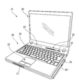
- FIG. 1 is an external perspective view of a notebook PC, which is an embodiment of the electronic apparatus of the present case, in an open state.
- 2 is a six-side view of the notebook PC shown in FIG. 1 in a closed state.
- 3 is a perspective view of the main unit of the notebook PC shown in FIGS. 1 and 2
- FIG. 4 is a six-side view of the main unit.
- 2A and 2B, (A) to (F) are respectively a plan view (A), a left side view (B), a right side view (C), a rear view (D), a front view (E), It is a bottom view (F).
- the notebook PC 10 includes a main unit 20 and a display unit 30.
- the display unit 30 is supported by the main unit 20 so as to be freely opened and closed between an open state shown in FIG. 1 and a closed state shown in FIG.
- the main unit 20 has a side surface that wraps around the upper surface and the bottom surface and the periphery of the top surface and the bottom surface by the housing member 520 on the bottom surface side and the housing member 530 on the top surface side and defines an internal space together with the top surface and the bottom surface
- a housing 510 is formed.
- the right side has an opening in which an optical disk drive (hereinafter abbreviated as “ODD”) 26 is accommodated by a slide. From the opening, an outer surface 261 of the accommodated ODD 26 can be seen.
- ODD optical disk drive
- An air inlet 27 is formed in the front end surface of the main unit 20. Further, an exhaust port 28 is provided on the left side surface of the main unit 20.
- the main unit 20 has a built-in fan 41 (see, for example, FIG. 11). When the fan 41 rotates, air is sucked from the air inlet 27 and the internal electronic components are cooled by air and exhausted from the air outlet 28.
- Various connectors and the like are arranged on the left side surface of the main unit 20 in addition to the exhaust port 27. A detailed description of the connector type and arrangement position will be omitted.
- FIG. 3 (F) shows a lid 29 covering the opening.
- a CPU Central Processing Unit for executing a program is mounted.
- main unit 20 arithmetic processing corresponding to the program is executed by executing the program in the CPU.
- HDD storage method In this description, the HDD is exemplified, and another auxiliary storage device such as an SSD (Solid State Drive) may be used instead of the HDD.
- This SSD uses a flash memory as a recording medium, but has the same external structure as an HDD and is a replacement part like an HDD. Further, other types of electronic components having the same external structure may be used instead of the auxiliary storage device.
- FIG. 5 shows a layout of HDD and ODD, which is a notebook PC as a comparative example.
- FIG. 6 is a diagram showing a method of housing the HDD in the notebook PC of the comparative example shown in FIG.
- FIG. 5 shows the HDD 42 in the stored state and the ODD 26 before being stored in the ODD storage unit 501.
- the fan 41 and other various parts are arranged in addition to those, but description thereof will be omitted here.
- the ODD 26 is stored in the ODD storage portion 501 by sliding in the direction of the arrow A from the ODD storage opening 502 provided on the side surface of the main unit.
- the HDD 42 is housed in an HDD housing opening 503 provided on the bottom surface of the main unit.
- the HDD 42 is provided with a connector 421 (see FIG. 9) on the front end surface 42a
- the HDD 42 is first placed in the HDD storage opening 503 (in the direction of arrow B) as shown in FIG. Movement).
- the HDD 42 is further slid in the direction of arrow C, and the connector 421 on the front end face 42a is assembled with a main body side connector (not shown). Therefore, a gap 504 shown in FIG. 5 is formed in the HDD housing opening 503 on the rear end face side of the HDD 42.
- the gap 504 is an unnecessary gap until the HDD 42 needs to be replaced after the HDD 42 is accommodated in the main unit. However, since it is necessary at the time of storage or replacement, it is not possible to place other parts or the like in the gap 504, and the gap 504 remains dead when the notebook PC is in operation. Space.
- FIG. 7 and 8 are a perspective view and a plan view, respectively, showing a method for connecting the ODD and the HDD in the notebook PC of the present embodiment.
- the ODD 26 roughly includes an ODD main body 260 and a circuit board 60.
- the ODD main body 260 has a function of accessing a disk-shaped optical disk while being detachably loaded and rotating the loaded optical disk.
- a connector 261 is provided on the front end surface of the ODD main body 260 to receive power from the outside of the ODD main body 260 and to exchange signals between the ODD main body 260 and the outside.
- the ODD main body 260 includes a fixing bracket 61 provided with a screw hole 611 and a flange 612 for supporting the circuit board 60, and a fixing bracket 62 provided with a screw hole 621. These fixing brackets 61 and 62 are fixed to the side surface of the ODD main body 260 with screws.
- one of the fixing brackets 61 and 62 has two fixing tongues 613 on one side surface of the ODD main body 260. These two fixed tongue pieces 613 are at substantially the same height as the lower surface of FIG. 7 (the upper surface of FIG. 8) of the ODD main body 260, and a screw hole 613a is formed at the center of each fixed tongue piece 613. Yes.
- the ODD 26 is screwed from the bottom side to a bottom case member constituting the casing of the main unit 20 (see FIG. 1) by using screw holes 613a provided in the fixed tongue pieces 613.
- the other fixing bracket 62 has one fixing tongue 623 on the other side surface of the ODD main body 260. This fixed tongue piece 623 is also for fixing the ODD 26.
- the fixed tongue 623 is at a height position near the upper surface of FIG. 7 (the lower surface of FIG. 8) of the ODD main body 260, and the hole 623a provided in the center is not a screw hole but a simple through hole.
- the fixed tongue piece 623 is sandwiched between a bottom-side casing member and a top-side casing member constituting the casing of the main unit 20, and a screw inserted from the bottom-side casing member passes through the hole 623 a.
- the upper casing member is fixed with screws, it is fastened together. Details of the method of fixing the ODD 26 will be described later. In this way, by tightening only some of the fixed tongue pieces, the number of fixing screws can be reduced accordingly, and the number of assembly steps can also be reduced.
- the HDD 42 includes a disk-shaped hard disk (not shown).
- the HDD 42 has a function of accessing a built-in disk-shaped hard disk while rotating it with a motor.
- the HDD 42 has a connector 421 on its front end surface.
- the connector 421 is a connector that receives power supply from the outside of the HDD 42 and exchanges signals between the HDD 42 and the outside.
- the circuit board 60 is a component constituting the ODD 26 and is screwed into two screw holes 611 and 621 provided one by one on the fixing brackets 61 and 62 on the ODD main body 260 side by two screws 605.
- the connector 604 which will be described later, is screwed so as to be sandwiched between the flange portions 612 of the fixing bracket 61 (see FIG. 22).
- a connector 602 that is assembled with the connector 421 is mounted at a position facing the connector 421 provided on the front end surface of the HDD 42.
- a connector 603 that is assembled with the connector 261 is mounted on the circuit board 60 at a position facing the connector 261 provided on the front end surface of the ODD main body 260.
- Another connector 604 is also mounted on the circuit board 60.
- the connector 604 is connected to the other two connectors 602 and 603 by wiring (not shown) on the circuit board 60.
- the connector 604 is connected to electronic circuit elements other than the HDD 42 and the ODD 26 in the main unit 20 (see FIG. 1), receives power supplied to the HDD 42 and the ODD 26, and connects the signal lines of both the HDD 42 and the ODD 26 to the other components. It plays a role of connecting with electronic circuit elements.
- the connector 604 is connected to one end of a flexible substrate (FFC) 606 (see FIGS. 22 and 24) not shown here and connected to an external electronic circuit element via the FFC 606.
- FFC flexible substrate
- FIG. 9 is an exploded perspective view showing the bottom surface side of the main unit and an exploded view of the HDD and the lid.
- FIG. 10 is a perspective view of the same notebook PC as FIG. 1 in the open state.
- FIG. 11 is a plan view showing the inside viewed from the bottom side with the casing member covering the bottom side of the main unit being removed
- FIG. 12 is a cross-sectional view taken along arrow AA shown in FIG.
- the ODD is slightly protruded from the housing of the main unit.
- an opening 202 for housing the HDD 202 is formed on the bottom surface 201 of the main unit 20.
- the HDD 42 is housed in the housing of the main unit 20 through the opening 202.
- the ODD 26 is slightly eaten from the opening 203 formed on the side surface (the right side surface shown in FIG. 10) of the main body unit 20.
- the HDD 42 is housed in the housing of the main unit 20 through the opening 202 in a protruding state.
- the HDD 42 interferes with the connector 602 mounted on the circuit board 60 on the ODD 26 side due to the space created in the housing of the main unit 20 due to the ODD 26 protruding slightly from the side surface of the main unit. Without being accommodated in the housing of the main unit 20 through the opening 202.
- FIG. 13 is a plan view showing the inside as viewed from the bottom surface side by removing the casing member that covers the bottom surface side of the main unit, as in FIG. Here, the ODD 26 is pushed into the main unit housing.
- 14 is a cross-sectional view taken along the arrow AA shown in FIG. 13 in the state shown in FIG.
- the HDD 42 is housed in the housing of the main unit 20 through the opening 202 with the connector 421 on the front end surface of the HDD 42 facing the ODD 26 side when the ODD 26 is slightly protruding. Thereafter, the ODD 26 is pushed until the outer surface 261 is flush with the casing side surface of the main unit 20. Then, as described with reference to FIGS. 7 and 8, the connector 602 mounted on the circuit board 60 screwed to the ODD main body 260 and the connector 421 provided on the front end surface of the HDD 42 are coupled. As a result, the ODD 26 is stored in the housing of the main unit 20.
- the HDD 24 is accommodated by using the space generated when the ODD 26 protrudes from the main unit housing, so that the HDD 24 can be opened only by linear movement in a direction perpendicular to the opening 202. It is stored in 202. That is, unlike the comparative example described with reference to FIGS. 5 and 6, there is no need to slide the HDD 42 after the HDD 42 is inserted into the housing through the frontage, and a useless space is formed in the HDD housing opening. Can be avoided.
- the opening 202 in which the HDD 42 is accommodated is covered with a lid 29.
- the lid body 29 is fixed to the lid body by screwing.
- screws are inserted into the three mounting holes 521a and 522 (see also FIG. 21) on the bottom surface and fixed by screwing.
- FIG. 15 and FIG. 16 are a perspective view and a plan view, respectively, showing the interior from the top side by removing the keyboard covering the top side of the main unit and the casing member on the top side.
- FIG. 17 is a cross-sectional view taken along arrow BB shown in FIG.
- the ODD 26 is in a state of protruding from the side surface of the main unit.
- the connector 604 is mounted on the circuit board 60 shown in FIGS.
- the connector 604 is connected to electronic circuit elements other than the HDD 42 and the ODD 26 via the FFC 606 (see FIG. 17).
- the connector 604 includes a flap that holds the FFC 606 between the connector main body and the connector main body to maintain the electrical connection between the terminal of the FFC 606 and the terminal of the connector.
- a mating connector 512 is mounted on a memory board 511 on which a memory is mounted.
- the connector 604 on the circuit board 60 on the ODD 26 side and the connector 512 on the memory board 511 are connected to the FFC 606. Connected through.
- the ODD 26 protrudes from the side surface of the main unit, and in this state, the connector 604 receives a pulling force in the direction in which the connector 604 is peeled off from the circuit board 60 due to the rigidity of the FFC 606. .
- the flange portion 612 provided on the mounting bracket 61 shown in FIG. 7 and the like supports the connector 604, thereby suppressing the occurrence of defects such as peeling of the connector 604 from the circuit board 60 due to this tensile force. Further, the flange portion 612 prevents the flap from being detached from the connector main body due to the reaction force of the FFC 606. As a result, the flange 612 also has an effect of preventing the FFC 606 from coming off.
- FIG. 18, FIG. 19, and FIG. 20 are diagrams corresponding to FIG. 15, FIG. 16, and FIG. 17, respectively, in a state where the ODD is pushed into the main unit.
- the FFC 606 is folded as shown in FIG. At this time, the connector 421 on the HDD side and the connector 602 on the circuit board on the ODD side are coupled (see FIG. 14).
- FIG. 21 is a diagram showing a space in the main unit in which the ODD is arranged.
- a housing member 520 on the bottom surface side constituting the housing of the main unit is shown.
- the ODD (not shown in FIG. 21) is stored in the ODD storage unit 501 by sliding from the side of the main unit. A total of three ODDs stored in the ODD storage unit 501 pass through the mounting holes 521a formed in the bosses 521 provided on the bottom side casing member 520 and the two mounting holes 522 formed in the bottom. Screw (not shown).
- FIG. 22 is a perspective view of the ODD as seen from the upper surface side.
- FIG. 23 is a perspective view of the ODD as seen from the bottom side.
- FIG. 22 shows a state in which the circuit board 60 is fixed, and
- FIG. 23 shows an ODD main body with the circuit board removed.
- the mounting bracket 62 has the mounting tongue 623 at a height position close to the upper surface of the ODD 26, and the mounting tongue 623 has a hole 623 a formed therein. .
- the mounting tongue 623 rides on the boss 521, and the hole 623a formed in the mounting tongue 623 and the hole 521a formed in the boss 521 Communicate.
- a top surface side housing member 530 (see FIGS. 26 and 27) that constitutes the housing of the main unit 20 is placed thereon, and the top surface is covered by screws inserted from the bottom surface of the bottom surface side housing member 520.
- the side casing member 530 is fixed to the bottom casing member 520. At the same time, the portion of the mounting tongue 62 of the mounting bracket 62 of the ODD 26 is fastened together with the housing member 520 on the bottom surface side together with the housing member 530 on the top surface side.
- the other mounting bracket 61 has two mounting tongues 613 at substantially the same height as the bottom surface of the ODD main body. Screw holes 613a are formed in the two attachment tongue pieces 613, respectively.
- these two mounting tongues 613 ride on the two mounting holes 522 at the bottom of the bottom-side casing member 520, and the mounting tongue 613
- the screw hole 613 a communicates with the mounting hole 522.
- a screw is inserted from the bottom surface of the housing member 520 on the bottom surface side, and the mounting tongue piece 613 is fixed to the housing member 520 on the bottom surface side by the screw.
- the fixing of the attachment tongue 613 is independent of the fixing of the housing member 530 on the upper surface side.
- FIG. 24 and 25 are plan views showing the inside of the main unit by removing the upper surface side casing member.
- FIG. 24 shows a state where the ODD protrudes from the side surface of the main unit
- FIG. 25 shows a state where the ODD is stored in the main unit.
- the mounting tongue piece 623 when the ODD 26 protrudes from the side surface of the main unit, the mounting tongue piece 623 is in a position away from the boss 521 provided on the bottom casing member 520.
- the attachment tongue 623 overlaps the boss 521, and the hole 623a provided in the attachment tongue 623 communicates with the attachment hole 521a provided in the boss.
- FIG. 26 is a plan view showing a state where the main body unit in the state shown in FIG.
- FIG. 27 is a diagram showing the main body units arranged side by side with the inner surface of the upper casing member facing upward and the upper casing member removed.
- a sheet metal member 531 spreads on the inner surface of the housing member 530 on the upper surface side. As shown in FIG. 26, the sheet metal member 531 is covered with the hole 521a (FIG. 24) of the boss 521 of the bottom member 520 when the top member 530 is covered so as to cover the top surface of the main unit. A screw hole 531a is provided at a position overlapping with the reference).
- the upper housing member 530 is placed on the ODD 26 and a screw is inserted into the mounting hole 521a of the boss 521 from the lower housing member 520.
- the housing member 530 and the ODD 26 on the upper surface side are fastened together with the housing member 520 on the bottom surface side by passing through the hole 623a of the mounting tongue piece 623 and screwing into the screw hole 531.
- the ODD 26 is fixed not only to the attachment tongue 623 but also to the two attachment tongues 613 (see FIG. 23).
- the upper surface side housing member 530 is screwed to the bottom surface side housing member 520 at locations other than the joint tightening portion of the mounting tongue 623, but is screwed at locations other than the joint tightening portion with the ODD 26. The description about is omitted.
- a keyboard 24 (see, for example, FIG. 1) is further placed on the top case member 530 fixed to the bottom case member 520 to complete the main unit as shown in FIG.
- the ODD 26 has the mounting tongue piece 623 fastened together, and by this fastening, the number of screws and the number of assembly steps are reduced.
- FIG. 28 is a diagram illustrating a notebook PC as a comparative example, which is an FPC that connects connectors together.
- the first side of the FPC 81 is inserted and electrically connected to one of the two connectors 71 and 72.
- the second side of the FPC 81 is inserted into and electrically connected to the other connector 72 of the two connectors 71 and 72.
- the region of the connector 71 and the FPC 81 in the vicinity of the first side inserted into the connector 71 is fixed by the adhesive tape 91.
- the area of the connector 72 and the FPC 81 in the vicinity of the second side inserted into the connector 72 is fixed by the adhesive tape 92.
- the first side and the second side of the FPC 82 are inserted into the connectors 73 and 74, respectively, and the two connectors 73 and 74 are electrically connected via the FPC 82. ing. Further, an adhesive tape 93 is affixed to the upper portion of the connector 73 and the periphery thereof to prevent the FPC 82 from coming off from the connector 73.
- the FPC is prevented from coming off from the connector without adding another part.
- FIG. 29 is a diagram showing the inside of the notebook PC of the present embodiment as viewed from the upper surface side of the main unit 20 with the casing member on the upper surface side removed.
- 30 is a cross-sectional view taken along the arrow AA shown in FIG. 29, and
- FIG. 31 is a cross-sectional view taken along the arrow BB shown in FIG.
- FIG. 29 shows two connectors 75 and 76 and an FPC 83.
- the FPC 83 has a first side inserted into the connector 75 and a second side inserted into the connector 76 to electrically connect the two connectors 75 and 76.
- the FPC 83 that connects the two connectors 75 and 76 does not connect the two connectors 75 and 76 linearly, and the first side inserted into the connector 75 and the connector 76 as shown in FIG. It has a shape detoured in a mountain shape between the second side inserted into the. Further, as shown in FIG. 29, the planar shape of the FPC 83 is also formed irregularly (non-rotationally symmetric).
- FIG. 29 further shows two connectors 77 and 78 and an FPC 84.
- the FPC 84 has a first side inserted into the connector 77 and a second side inserted into the connector 78 to electrically connect the two connectors 77 and 78.
- the two connectors 77 and 78 are arranged with a step as shown in FIG. 31, and the FPC 84 connecting the two connectors 77 and 78 also has the two connectors 77 and 78 with a step. It has a shape in which a step is formed in the middle so as to connect the two.
- the FPC 84 has a shape having a larger step than the two connectors 77 and 78, and the shape swells upward accordingly.
- the FPC 84 has an irregular shape (non-rotating object) having a tongue piece 841 spreading laterally as shown in FIG.
- a component 95 is mounted at a position adjacent to the FPC 84. The meaning of the component 95 being mounted here will be described later.
- FIG. 32 is a perspective view of the vicinity of one FPC 83 of the two FPCs.
- FIG. 33 is a perspective view of the FPC 83
- FIG. 34 (A) to (F) are respectively a plan view (A), a left side view (B), a right side view (C), a rear view (D), a front view (E), and a bottom view ( F).
- the two connectors 75 and 76 are arranged in a posture in which the insertion port into which the FPC 83 is inserted is directed in a direction facing each other, and each side of the FPC 83 is inserted from the side surface on the side facing each other.
- the FPC 83 has a shape in which the central portion is swollen. Further, as shown in a plan view (A) and a bottom view (F) in FIG.
- FIG. 35 is a cross-sectional view of the portion indicated by arrow AA in FIG. 29 in a state where the upper surface casing member 530 is put on the FPC shown in FIGS. 32 to 34 and the keyboard 24 is arranged. is there.
- the center bulge portion is pushed by the casing member 530 on the upper surface side.
- the FPC 83 has a certain degree of rigidity, and when the center swelled portion is pushed, the FPC 83 opens to the first side and the second side of the FPC 83 in a direction in which the first side and the second side are separated from each other. It has the power to do. Therefore, a force is applied to the first side and the second side of the FPC 83 in the direction in which the two connectors 75 and 76 are inserted. For this reason, the insertion of the FPC 83 into each of the connectors 75 and 76 is reliably ensured without adding another part or adopting a connector with a special lock.
- FIG. 36 and 37 are a perspective view and a hexahedral view, respectively, showing an FPC as a modification.
- FIG. 37 (A) to (F) are respectively a plan view (A), a left side view (B), a right side view (C), a rear view (D), and a front view (E). ) And a bottom view (F).
- the FPCs shown in FIGS. 33 and 34 have a mountain-shaped shape, but the FPCs shown in FIGS. 36 and 37 have a shape that bulges in a mountain shape. Even if the FPC has the shape shown in FIGS. 36 and 37, it has an effect of ensuring the connection with the connector by forming it at a height at which the top of the chevron is pushed.
- FIG. 38 is a perspective view of a region in the vicinity of the other FPC 84 of the two FPCs.
- 39 and 40 are a perspective view and a six-sided view of the FPC 84 itself.
- 40 (A) to (F) are a plan view (A), a left side view (B), a right side view (C), a rear view (D), a front view (E), and a bottom view, respectively. (F).
- the two connectors 77 and 78 connected by the FPC 84 are arranged in such a manner that the insertion ports face each other and have steps.
- the step shown in FIG. 40B is larger than the step between the two connectors 77 and 78 connected by the FPC 84 (see FIG. 31). Therefore, as shown in FIG. 38, when the two connectors 77 and 78 are connected by the FPC 84, the FPC 84 has a shape swelled in a mountain shape.
- the portion swelled in a mountain shape is pushed onto the upper surface of the housing, like the other FPC 83, and receives a force in a direction in which the first side and the second side of the FPC 83 are strongly inserted by the connectors 77 and 78.
- the FPC 84 is strongly inserted by the connectors 77 and 78, and the FPC is prevented from being detached from the connector due to some vibration or the like.
- 41 and 42 are a perspective view and a six-sided view of a modified FPC.
- 42, (A) to (F) are a plan view (A), a left side view (B), a right side view (C), a rear view (D), a front view (E), and a bottom view, respectively. (F).
- a step is formed by angular bending, but in the case of the FPC shown in FIGS. 41 and 42, a step is provided between the first side and the second side.
- the central portion has a rounded shape.
- the FPC is pushed on the top surface of the housing, but the FPC is not a housing itself but a member that has a surface that extends across two connectors connected by the FPC. It is good also as a structure which arrange
- FIG. 43 is a diagram showing two FPCs in a reverse connection state.
- FIG. 43 is a perspective view of a region near one FPC 83 of the two FPCs.
- the FPC 83 that connects the two connectors 75 and 76 is an FPC whose first side is intended to be inserted into the connector 75 and whose second side is intended to be inserted into the connector 76.
- This correct connection is referred to as a forward connection here. .
- the second side of the FPC 83 is inserted into the connector 75, and the first side is placed in a direction to be inserted into the connector 76.
- this is called reverse connection.
- the portion 831 protruding laterally of the FPC 83 hits the member 94 standing in the casing, and the FPC 83 cannot be inserted into both the two connectors 75 and 76.
- forward connection as shown in FIG. 32, the FPC 83 can be correctly inserted into both of the two connectors 75 and 76 without interfering with others. As a result, the assembly operator of this notebook PC can be made to recognize the reverse connection.
- the other FPC 84 shown in FIG. 43 is also in a reverse connection state.
- the FPC 84 has a tongue piece 841.
- the tongue piece 841 rides on the component 95, and when the FPC 84 is forcibly inserted into the connector 77, the tongue piece 841 is lifted as shown in FIG. .
- forward connection for example, as shown in FIG. 38, it does not interfere with other members or parts, and the tongue 841 does not have a particularly raised shape. Due to the deformation of the FPC, the assembly operator recognizes that the connection is reverse.
- FIG. 45 is a diagram showing a modification around the FPC.
- a screw hole 96 is formed at a position adjacent to the FPC 841.
- the FPC 84 is in the forward connection state, but when the FPC 83 is reversely connected, the tongue piece 841 of the FPC 83 covers the hole 96 and covers the hole 96.
- the screwing work using the hole 96 is a work after the connecting work of the connectors 77 and 78 by the FPC 83. Therefore, if the FPC 84 is reversely connected, the screwing work cannot be performed. As a result, the assembly operator recognizes that the FPC 84 is reversely connected.
- the reverse connection can be recognized only by the shape of the FPC and its surrounding parts, members, holes, etc. without increasing the cost such as adopting a connector having a special structure.
Abstract
L'invention porte sur un dispositif électronique, comportant un circuit imprimé souple (FPC), reliant électriquement un premier connecteur à un deuxième connecteur pour empêcher le FPC de se détacher, sans devoir recourir à un composant additionnel ou à un connecteur de structure spéciale, et formé entre un premier côté du FPC inséré dans le premier connecteur et le deuxième côté du FPC inséré dans le deuxième connecteur de manière à être dévié vers un élément distant du premier et du deuxième connecteur, et s'étendant le long du premier connecteur et du deuxième connecteur, jusqu'à ce qu'il entre en contact avec ledit élément. Le FPC présente une rigidité grâce à laquelle, lorsqu'il est poussé par ledit élément suite à son contact avec ledit élément, le premier côté et le deuxième côté sont poussés dans la direction d'insertion du premier connecteur et du deuxième connecteur.
Priority Applications (2)
| Application Number | Priority Date | Filing Date | Title |
|---|---|---|---|
| JP2011528592A JPWO2011024317A1 (ja) | 2009-08-31 | 2009-08-31 | 電子機器 |
| PCT/JP2009/065216 WO2011024317A1 (fr) | 2009-08-31 | 2009-08-31 | Dispositif électronique |
Applications Claiming Priority (1)
| Application Number | Priority Date | Filing Date | Title |
|---|---|---|---|
| PCT/JP2009/065216 WO2011024317A1 (fr) | 2009-08-31 | 2009-08-31 | Dispositif électronique |
Publications (1)
| Publication Number | Publication Date |
|---|---|
| WO2011024317A1 true WO2011024317A1 (fr) | 2011-03-03 |
Family
ID=43627441
Family Applications (1)
| Application Number | Title | Priority Date | Filing Date |
|---|---|---|---|
| PCT/JP2009/065216 WO2011024317A1 (fr) | 2009-08-31 | 2009-08-31 | Dispositif électronique |
Country Status (2)
| Country | Link |
|---|---|
| JP (1) | JPWO2011024317A1 (fr) |
| WO (1) | WO2011024317A1 (fr) |
Cited By (3)
| Publication number | Priority date | Publication date | Assignee | Title |
|---|---|---|---|---|
| JP2013197129A (ja) * | 2012-03-16 | 2013-09-30 | Ricoh Co Ltd | プリント基板の接続構造とその接続用のfpc及び電子機器 |
| JP2014211956A (ja) * | 2013-04-17 | 2014-11-13 | リコーイメージング株式会社 | フレキシブルプリント基板の誤挿入防止装置 |
| JP2014228882A (ja) * | 2013-05-17 | 2014-12-08 | Necパーソナルコンピュータ株式会社 | ノート型コンピュータ |
Citations (5)
| Publication number | Priority date | Publication date | Assignee | Title |
|---|---|---|---|---|
| JPH01174866U (fr) * | 1988-05-27 | 1989-12-12 | ||
| JPH04155415A (ja) * | 1990-10-18 | 1992-05-28 | Nippon Steel Corp | 携帯型パーソナルコンピュータ |
| JP2000294329A (ja) * | 1999-04-08 | 2000-10-20 | Yazaki Corp | フレキシブル配線板の回路基板接続構造 |
| JP2008084217A (ja) * | 2006-09-28 | 2008-04-10 | Fujitsu Ltd | 電子機器および板金部材 |
| JP2008287918A (ja) * | 2007-05-15 | 2008-11-27 | Calsonic Kansei Corp | 車両用電子基板モジュール構造 |
-
2009
- 2009-08-31 JP JP2011528592A patent/JPWO2011024317A1/ja active Pending
- 2009-08-31 WO PCT/JP2009/065216 patent/WO2011024317A1/fr active Application Filing
Patent Citations (5)
| Publication number | Priority date | Publication date | Assignee | Title |
|---|---|---|---|---|
| JPH01174866U (fr) * | 1988-05-27 | 1989-12-12 | ||
| JPH04155415A (ja) * | 1990-10-18 | 1992-05-28 | Nippon Steel Corp | 携帯型パーソナルコンピュータ |
| JP2000294329A (ja) * | 1999-04-08 | 2000-10-20 | Yazaki Corp | フレキシブル配線板の回路基板接続構造 |
| JP2008084217A (ja) * | 2006-09-28 | 2008-04-10 | Fujitsu Ltd | 電子機器および板金部材 |
| JP2008287918A (ja) * | 2007-05-15 | 2008-11-27 | Calsonic Kansei Corp | 車両用電子基板モジュール構造 |
Cited By (3)
| Publication number | Priority date | Publication date | Assignee | Title |
|---|---|---|---|---|
| JP2013197129A (ja) * | 2012-03-16 | 2013-09-30 | Ricoh Co Ltd | プリント基板の接続構造とその接続用のfpc及び電子機器 |
| JP2014211956A (ja) * | 2013-04-17 | 2014-11-13 | リコーイメージング株式会社 | フレキシブルプリント基板の誤挿入防止装置 |
| JP2014228882A (ja) * | 2013-05-17 | 2014-12-08 | Necパーソナルコンピュータ株式会社 | ノート型コンピュータ |
Also Published As
| Publication number | Publication date |
|---|---|
| JPWO2011024317A1 (ja) | 2013-01-24 |
Similar Documents
| Publication | Publication Date | Title |
|---|---|---|
| JP4842898B2 (ja) | 電子機器 | |
| JP4847414B2 (ja) | 電子部品取付用部品および電子機器 | |
| KR100989085B1 (ko) | 표시 장치 및 전자 기기 | |
| JP2008141139A (ja) | 電子機器、フレキシブル基板および基板固定部材 | |
| US7733638B2 (en) | Electronic apparatus | |
| KR100969895B1 (ko) | 전자 기기 | |
| JP2009163292A (ja) | 電子機器 | |
| US8009423B2 (en) | Electronic device | |
| US8059393B2 (en) | Electronic apparatus | |
| JP2005157790A (ja) | 電子機器 | |
| US20090168384A1 (en) | Electronic apparatus | |
| WO2011024317A1 (fr) | Dispositif électronique | |
| WO2011024316A1 (fr) | Appareil électronique | |
| JP2007048085A (ja) | 電子機器 | |
| JP5532049B2 (ja) | 電子機器 | |
| JP4922241B2 (ja) | 電子機器 | |
| JP5061782B2 (ja) | 電子機器 | |
| WO2011067844A1 (fr) | Dispositif électronique | |
| US7848092B2 (en) | Electronic apparatus and display panel enclosure | |
| JP2016042259A (ja) | 電子機器及び支持部材 |
Legal Events
| Date | Code | Title | Description |
|---|---|---|---|
| 121 | Ep: the epo has been informed by wipo that ep was designated in this application |
Ref document number: 09848762 Country of ref document: EP Kind code of ref document: A1 |
|
| WWE | Wipo information: entry into national phase |
Ref document number: 2011528592 Country of ref document: JP |
|
| NENP | Non-entry into the national phase |
Ref country code: DE |
|
| 122 | Ep: pct application non-entry in european phase |
Ref document number: 09848762 Country of ref document: EP Kind code of ref document: A1 |