WO2011004533A1 - 荷電粒子線装置 - Google Patents
荷電粒子線装置 Download PDFInfo
- Publication number
- WO2011004533A1 WO2011004533A1 PCT/JP2010/003257 JP2010003257W WO2011004533A1 WO 2011004533 A1 WO2011004533 A1 WO 2011004533A1 JP 2010003257 W JP2010003257 W JP 2010003257W WO 2011004533 A1 WO2011004533 A1 WO 2011004533A1
- Authority
- WO
- WIPO (PCT)
- Prior art keywords
- charged particle
- wafer
- particle beam
- beam apparatus
- temperature
- Prior art date
- Legal status (The legal status is an assumption and is not a legal conclusion. Google has not performed a legal analysis and makes no representation as to the accuracy of the status listed.)
- Ceased
Links
Images




Classifications
-
- G—PHYSICS
- G01—MEASURING; TESTING
- G01N—INVESTIGATING OR ANALYSING MATERIALS BY DETERMINING THEIR CHEMICAL OR PHYSICAL PROPERTIES
- G01N23/00—Investigating or analysing materials by the use of wave or particle radiation, e.g. X-rays or neutrons, not covered by groups G01N3/00 – G01N17/00, G01N21/00 or G01N22/00
- G01N23/22—Investigating or analysing materials by the use of wave or particle radiation, e.g. X-rays or neutrons, not covered by groups G01N3/00 – G01N17/00, G01N21/00 or G01N22/00 by measuring secondary emission from the material
- G01N23/225—Investigating or analysing materials by the use of wave or particle radiation, e.g. X-rays or neutrons, not covered by groups G01N3/00 – G01N17/00, G01N21/00 or G01N22/00 by measuring secondary emission from the material using electron or ion
- G01N23/2251—Investigating or analysing materials by the use of wave or particle radiation, e.g. X-rays or neutrons, not covered by groups G01N3/00 – G01N17/00, G01N21/00 or G01N22/00 by measuring secondary emission from the material using electron or ion using incident electron beams, e.g. scanning electron microscopy [SEM]
-
- H—ELECTRICITY
- H01—ELECTRIC ELEMENTS
- H01J—ELECTRIC DISCHARGE TUBES OR DISCHARGE LAMPS
- H01J37/00—Discharge tubes with provision for introducing objects or material to be exposed to the discharge, e.g. for the purpose of examination or processing thereof
- H01J37/02—Details
- H01J37/20—Means for supporting or positioning the object or the material; Means for adjusting diaphragms or lenses associated with the support
-
- H—ELECTRICITY
- H01—ELECTRIC ELEMENTS
- H01J—ELECTRIC DISCHARGE TUBES OR DISCHARGE LAMPS
- H01J37/00—Discharge tubes with provision for introducing objects or material to be exposed to the discharge, e.g. for the purpose of examination or processing thereof
- H01J37/26—Electron or ion microscopes; Electron or ion diffraction tubes
- H01J37/261—Details
- H01J37/265—Controlling the tube; circuit arrangements adapted to a particular application not otherwise provided, e.g. bright-field-dark-field illumination
-
- H—ELECTRICITY
- H01—ELECTRIC ELEMENTS
- H01J—ELECTRIC DISCHARGE TUBES OR DISCHARGE LAMPS
- H01J37/00—Discharge tubes with provision for introducing objects or material to be exposed to the discharge, e.g. for the purpose of examination or processing thereof
- H01J37/26—Electron or ion microscopes; Electron or ion diffraction tubes
- H01J37/28—Electron or ion microscopes; Electron or ion diffraction tubes with scanning beams
-
- H—ELECTRICITY
- H01—ELECTRIC ELEMENTS
- H01J—ELECTRIC DISCHARGE TUBES OR DISCHARGE LAMPS
- H01J37/00—Discharge tubes with provision for introducing objects or material to be exposed to the discharge, e.g. for the purpose of examination or processing thereof
- H01J37/30—Electron-beam or ion-beam tubes for localised treatment of objects
- H01J37/305—Electron-beam or ion-beam tubes for localised treatment of objects for casting, melting, evaporating, or etching
- H01J37/3053—Electron-beam or ion-beam tubes for localised treatment of objects for casting, melting, evaporating, or etching for evaporating or etching
- H01J37/3056—Electron-beam or ion-beam tubes for localised treatment of objects for casting, melting, evaporating, or etching for evaporating or etching for microworking, e. g. etching of gratings or trimming of electrical components
-
- H—ELECTRICITY
- H10—SEMICONDUCTOR DEVICES; ELECTRIC SOLID-STATE DEVICES NOT OTHERWISE PROVIDED FOR
- H10P—GENERIC PROCESSES OR APPARATUS FOR THE MANUFACTURE OR TREATMENT OF DEVICES COVERED BY CLASS H10
- H10P72/00—Handling or holding of wafers, substrates or devices during manufacture or treatment thereof
- H10P72/06—Apparatus for monitoring, sorting, marking, testing or measuring
- H10P72/0602—Temperature monitoring
-
- G—PHYSICS
- G01—MEASURING; TESTING
- G01B—MEASURING LENGTH, THICKNESS OR SIMILAR LINEAR DIMENSIONS; MEASURING ANGLES; MEASURING AREAS; MEASURING IRREGULARITIES OF SURFACES OR CONTOURS
- G01B2210/00—Aspects not specifically covered by any group under G01B, e.g. of wheel alignment, caliper-like sensors
- G01B2210/56—Measuring geometric parameters of semiconductor structures, e.g. profile, critical dimensions or trench depth
-
- G—PHYSICS
- G01—MEASURING; TESTING
- G01N—INVESTIGATING OR ANALYSING MATERIALS BY DETERMINING THEIR CHEMICAL OR PHYSICAL PROPERTIES
- G01N2223/00—Investigating materials by wave or particle radiation
- G01N2223/30—Accessories, mechanical or electrical features
- G01N2223/31—Accessories, mechanical or electrical features temperature control
-
- G—PHYSICS
- G01—MEASURING; TESTING
- G01N—INVESTIGATING OR ANALYSING MATERIALS BY DETERMINING THEIR CHEMICAL OR PHYSICAL PROPERTIES
- G01N2223/00—Investigating materials by wave or particle radiation
- G01N2223/30—Accessories, mechanical or electrical features
- G01N2223/321—Accessories, mechanical or electrical features manipulator for positioning a part
-
- G—PHYSICS
- G01—MEASURING; TESTING
- G01N—INVESTIGATING OR ANALYSING MATERIALS BY DETERMINING THEIR CHEMICAL OR PHYSICAL PROPERTIES
- G01N2223/00—Investigating materials by wave or particle radiation
- G01N2223/60—Specific applications or type of materials
- G01N2223/611—Specific applications or type of materials patterned objects; electronic devices
- G01N2223/6116—Specific applications or type of materials patterned objects; electronic devices semiconductor wafer
-
- H—ELECTRICITY
- H01—ELECTRIC ELEMENTS
- H01J—ELECTRIC DISCHARGE TUBES OR DISCHARGE LAMPS
- H01J2237/00—Discharge tubes exposing object to beam, e.g. for analysis treatment, etching, imaging
- H01J2237/20—Positioning, supporting, modifying or maintaining the physical state of objects being observed or treated
- H01J2237/2001—Maintaining constant desired temperature
Definitions
- the present invention relates to a charged particle beam apparatus such as an electron microscope and an ion beam processing / observation apparatus, and a temperature adjusting means for a sample observed with the charged particle beam apparatus.
- a wafer is commercialized as a device through various apparatuses such as manufacturing, inspection, and evaluation.
- the wafer is mounted on a sample stage, and the sample stage is moved by a stage transfer device.
- the sample stage carries a wafer that has been transported from another apparatus, and the observation site of the wafer at a predetermined location within the apparatus, for example, the electron beam irradiation position of an electron microscope Need to be transported.
- wafers are processed across several types of manufacturing, inspection, and evaluation devices. However, since position reproducibility in the nano-order is required between each device, each device to be processed has a specific point. The origin is adjusted and aligned, a coordinate system in the current apparatus is created, and the wafer conveyance start timing and stop position are controlled based on the coordinate system.
- Patent Document 1 Japanese Patent Laid-Open No. 9-205080
- a Peltier element is embedded in a wafer facing surface of an electrostatic chuck that holds a wafer, and a thermocouple is disposed above the Peltier element (wafer facing surface).
- an invention is disclosed in which the Peltier device is controlled by the temperature of the wafer detected by a thermoelectric material.
- Patent Document 2 discloses a heating means and a temperature sensor disposed in an electrostatic chuck, and the heating means described above so as to correct partial distortion of the wafer due to electron beam heating.
- An invention of an exposure apparatus that overheats is disclosed.
- the reason why the temperature control technology for the wafer as described above has been developed in the semiconductor manufacturing apparatus is that, unlike the inspection / measurement in the case of manufacturing, there is a strict requirement for the accuracy of the beam irradiation position control because it cannot be redone.
- an inspection / measurement device in the case of a wafer inspection / measurement device using a charged particle beam, it is necessary to scan the sample with a primary charged particle beam that is as narrow as possible in order to obtain a high-resolution image. Since the beam current amount cannot be extremely increased in terms of the Coulomb effect, a wafer measurement / inspection device using a charged particle beam is less charged than a semiconductor manufacturing device. Since the energy is small, the misregistration due to the expansion of the wafer due to the heating of the charged particle beam was not a problem.
- JP-A-9-205080 (US Pat. No. 5,567,622) JP 2008-010259 A
- Wafer inspection / measurement apparatuses using charged particle beams are constantly required to increase the speed of wafer processing, that is, to shorten the time required for performing predetermined processing per semiconductor wafer.
- One of the biggest factors affecting the wafer processing throughput of various apparatuses is the wafer transfer speed.
- the stage conveyance device has a driving means such as a linear motor, an ultrasonic motor, or a combination of a ball screw and a pulse motor.
- a driving means such as a linear motor, an ultrasonic motor, or a combination of a ball screw and a pulse motor.
- thermocouple is brought into contact with the back surface of the wafer to detect the temperature of the wafer, but foreign matter is generated by the contact.
- the generated foreign material rises when the wafer is transported, which causes the foreign material to adhere to the wafer surface and cause contamination.
- foreign matter on the back surface of the wafer also becomes a problem. This is because a change in the height of the wafer due to the presence of foreign matter on the back surface may cause a focus shift.
- the quality of the object to be processed is not allowed to change before and after the inspection / measurement, so when performing wafer temperature control in a wafer inspection / measurement device using charged particle beams, It is required to measure the temperature of the wafer or the variation of the wafer size that can suppress the occurrence.
- the present invention provides a temperature adjusting means in a sample holding means for holding a semiconductor wafer as a sample, and a wafer observation index required for controlling the temperature adjusting means is contactless. It is characterized by comprising measuring means for obtaining.
- the temperature of the wafer 111 and the wafer holding mechanism does not change even if heat is generated due to any cause such as heat generation of the mechanism part due to continuous driving of the sample stage.
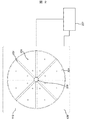
- FIG. 1 is a plan view showing an overall configuration of a scanning electron microscope that is an embodiment of the present invention.
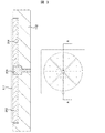
- FIG. 3 is a top view of a sample holder in the charged particle beam apparatus according to the first embodiment.
- FIG. 3 is a cross-sectional view of a sample holder in the charged particle beam apparatus according to the first embodiment.
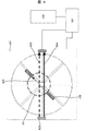
- FIG. FIG. 6 is a top view of a sample holder in the charged particle beam apparatus according to the second embodiment.
- FIG. 9 is a schematic diagram illustrating calculation of a defect position deviation amount according to a third embodiment.
- FIG. 10 is a detailed view related to a specific point display in a normal state according to the fourth embodiment.
- FIG. 10 is a detailed view related to a specific point position shift amount calculation according to the fourth embodiment.
- a configuration example of a charged particle beam apparatus provided with an infrared sensor as a measurement unit that acquires a wafer observation index necessary for controlling the temperature adjustment unit in a non-contact manner will be described.
- a scanning electron microscope having a function of detecting secondary electrons or reflected electrons generated by irradiating a wafer with a primary electron beam will be described as an example of the charged particle beam apparatus.
- FIG. 1 shows an overall view of the scanning electron microscope of this example.
- a general scanning electron microscope includes a column 101, a sample chamber 114, and a load lock chamber 115.
- a series of sequences for observing the wafer 111 to be observed will be described.
- the wafer 111 is transferred from a wafer transfer device (not shown) outside the apparatus, the atmosphere side gate valve 118 is opened, the wafer 111 is transferred into the load lock chamber 115, and the atmosphere side gate valve is closed. ),
- the load lock chamber 115 is evacuated.
- the vacuum side gate valve 116 is opened, and the wafer 111 is carried into the sample chamber 114 by the vacuum transfer robot 117.
- the wafer transfer from the load lock chamber 115 to the sample chamber 114 is executed by the vacuum transfer robot 117.
- the wafer 111 may be transferred into the sample chamber 114 using a wafer holder or the like. Absent.
- the wafer holding mechanism 112 may be mounted in the wafer holder, or the wafer holder itself may have a function equivalent to that of the wafer holding mechanism 112. Note that the inside of the sample chamber 114 is always kept evacuated.
- the wafer 111 carried into the sample chamber 114 is mounted on the wafer holding mechanism 112 on the sample stage 125.
- the sample stage 125 is driven via the stage control unit 121 using, for example, a conveying unit combining a ball screw and a pulse motor, or a conveying unit such as a linear motor or an ultrasonic motor.
- a bar mirror 124 is attached on the sample stage 125, and the position of the sample stage 125 is measured by measuring the relative distance between the interferometer 113 attached to the sample chamber 114 and the bar mirror 124 by laser measurement.
- the position control unit 120 performs processing to manage the position of the wafer 111 mounted and held on the sample stage 125.
- position detecting means such as a linear scale may be used.
- the charged particle beam 103 is generated from the electron gun 102 in the column 101, and the charged particle beam 103 passes through the electron lens 104 and the objective lens 108. Further, deflection coils 105 and 106 are provided in the column 101, and the charged particle beam 103 generated from the electron gun 102 is deflected to a predetermined activation by the deflection control unit 107. The charged particle beam 103 is converged by the objective lens 108 and irradiated onto the wafer 111. When the charged particle beam 103 is irradiated onto the wafer 111, reflected electrons and secondary electrons are generated and detected by the detector 110.
- the detection signals of reflected electrons and secondary electrons detected by the detector 110 are input to the image control unit 122 together with the control information of the charged particle beam 103 by the deflection coils 105 and 106.
- the image control unit 122 generates image data based on the above information and displays it on the monitor 123.
- the scanning electron microscope in this embodiment is equipped with a height detection sensor 109, which detects the detailed height of the wafer 111, which is an observation object, and charges the column control unit 119 based on the detected height.
- the deflection amount and convergence rate of the particle beam 103 are determined.
- a temperature adjustment mechanism control unit 207 for controlling temperature adjustment means provided on the sample stage 125 is disposed. The operation / function of the temperature adjustment mechanism control unit 207 will be described later.
- FIG. 2 shows a top view of the wafer holding mechanism 112 of this embodiment.
- the wafer 111 is transferred from a wafer transfer device (not shown), and after being transferred into the load lock chamber 115, it is evacuated. After completion of evacuation, the wafer 111 is transferred to the wafer holding mechanism 112 in the sample chamber 114, and is sucked and fixed to the electrostatic chucking plate 204 of the electrostatic chuck.
- an electrostatic chuck is used as the wafer 111 fixing means, but a mechanical chuck or the like may be used.
- a pusher pin 208 for peeling off the wafer after wafer processing and an opening for moving the pusher pin up and down are provided at the center of the electrostatic attraction plate 204, and a temperature adjusting mechanism 202 and a temperature measurement sensor 203 are provided around the pusher pin 208. Is arranged.
- a Peltier element having a plate-like upper electrode was used as a temperature adjusting mechanism, and the plate-like Peltier element was radially arranged around the pusher pin toward the outer periphery of the electrostatic chuck.
- the temperature measuring sensor 203 has a total of 16 points on the inner periphery around the center of the electrostatic suction plate, 8 points on the outer periphery near the end of the electrostatic suction plate, and a concentric circle around the pusher pin 208. Arranged. Since the wafer 111 on the electrostatic chucking plate 204 has no fulcrum, there is a high possibility that the wafer 111 will change radially when it expands and contracts due to a temperature change.
- the Peltier elements radially from the center, it is possible to deliver heat uniformly to the wafer, enabling smooth temperature adjustment, and applying extra stress to the wafer due to expansion and contraction. It becomes possible to prevent.
- the temperature measuring sensors radially, the wafer temperature can be measured uniformly, and accurate temperature information can be fed back to the Peltier element. By combining these, the temperature of the wafer 111 can be adjusted efficiently and in real time.
- the temperature measurement sensor 203 is attached inside the wafer holding mechanism 112 and measures the temperature of the wafer in a non-contact manner.
- the measured temperature is accumulated in the temperature adjustment mechanism control unit 207 via the cable inside the wafer holding mechanism 112, and the voltage applied to the Peltier element is calculated by the temperature adjustment mechanism control unit 207, and the electrostatic chucking plate is fed.
- a voltage is applied to the temperature adjustment mechanism 202 via the unit 209. Thereafter, the temperature is measured according to the interval set before the processing of the wafer 111, and the results are accumulated as needed.
- the temperature adjustment mechanism control unit 207 includes a memory element that stores temperature information and an arithmetic element that calculates an applied voltage to the Peltier element from the temperature information.
- FIGS. 3 and 4 show sectional views of the sample holding means of this embodiment.
- 3 is a cross-sectional view of the sample holding means shown in FIG. 2 cut along a cross-section (AA cross section) including a plate-like temperature control mechanism
- FIG. 4 is a top view of the sample holding means shown in FIG.
- FIG. 6 is a cross-sectional view taken along a cross section (BB cross section) including an infrared sensor.
- the electrostatic adsorption plate 204 is provided with a through hole for arranging an infrared sensor and a cable connected to the sensor.
- the infrared sensor is placed in the through hole while maintaining a distance that does not contact the wafer 111. Be placed.
- the surface of the electrostatic attraction plate 204 is provided with minute irregularities so that the generation of foreign matter is reduced. .
- the sample stage 125 repeatedly moves the measurement target position in the wafer 111 plane to the irradiation position of the charged particle beam 103 according to conditions.
- heat is generated from the drive unit, guide unit, and other contact units of the sample stage 125, and the temperature of the apparatus constituent members such as the sample stage 125 and the wafer holding mechanism 112 is increased. . Therefore, the sample stage is heated during wafer observation, and the temperature of the wafer mounted on the sample stage rises.
- the heated wafer expands according to the linear expansion coefficient, the coordinate system acquired by wafer alignment changes, and even if the sample stage is moved to the ideal position in its own coordinate system, the actual observation object is an electron beam. It will deviate from the irradiation position.
- the temperature adjustment mechanism control unit 207 determines the set temperature based on the temperature measurement result accumulated at any time, and the temperature adjustment mechanism so that the temperature of the wafer 111 is always constant. 202 is set to the specified temperature. With the above flow, temperature measurement and temperature adjustment of the wafer 111 are repeated as needed. Thereby, it is possible to prevent the temperature fluctuation of the wafer 111 from becoming larger than a predetermined value during the inspection / measurement of one wafer, and it is possible to suppress the displacement due to the expansion of the wafer.
- the temperature adjustment mechanism 202 may be a Peltier element or the like, but other temperature adjustment mechanisms may be used as long as they can be installed in a vacuum and have high temperature responsiveness.
- a temperature passage mechanism may be formed by forming a flow path through which the refrigerant passes in the electrostatic adsorption plate and circulating a suitable refrigerant, for example, a liquid such as helium gas, chlorofluorocarbon gas, or water in the flow path.
- a suitable refrigerant for example, a liquid such as helium gas, chlorofluorocarbon gas, or water in the flow path.
- the number of infrared sensor installation points is set to 16, but the number of installations may be reduced due to cost and mechanism arrangement restrictions.
- Si which is a main constituent element of the wafer 111, has a large thermal conductivity of about 150 [W / m ⁇ K]. .
- a charged particle beam apparatus having a configuration in which a wafer observation index (temperature in this case) is acquired in a non-contact manner using an infrared sensor has been described.
- a variation in wafer diameter is measured.
- a configuration example of a charged particle beam device that controls the temperature adjustment mechanism will be described.
- a scanning electron microscope will be described as an example of a charged particle beam apparatus.
- the overall configuration of the apparatus is substantially the same as that in FIG.
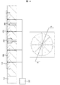
- FIG. 5 shows a cross-sectional view of the wafer holding mechanism 112 of this embodiment together with the end of the charged particle column 101.
- the charged particle beam apparatus according to the present embodiment includes a Peltier element including the same plate-like upper electrode as that of the first embodiment as a temperature adjustment mechanism, but does not include a temperature measurement sensor such as an infrared sensor. Therefore, as for the cross-sectional view of the wafer holding mechanism, only the cross-sectional view cut along the cross section including the plate-like electrode of the Peltier element is shown.
- the wafer 111 is transferred from a wafer transfer device (not shown), and is evacuated after being loaded into the load lock chamber 115. After evacuation, the wafer 111 is transferred onto the wafer holding mechanism 112. Thereafter, the diameter of the wafer 111 is measured by a pair of displacement sensors 504 installed on the wafer holding mechanism 112. Since the diameter of the wafer 111 to be inspected or measured is a value based on a standard such as 150, 200, 300, 450 mm, etc., by comparing with a certain normal range value, for example, cracking of the wafer 111 or conveyance failure It is also possible to detect such abnormalities.
- the displacement sensor 501 basically continues the wafer diameter measurement while the wafer 111 is being processed. In addition, the diameter measurement is performed at a cycle as short as possible, and data is accumulated in the temperature adjustment mechanism control unit 207.
- the temperature adjustment mechanism control unit 207 calculates a variation amount of the diameter of the wafer 111 from the accumulated measurement result, and determines a set temperature of the temperature adjustment mechanism 202. Thereby, the temperature of the wafer 111 is controlled.
- the displacement sensor of this embodiment is an optical type, and the laser beam emitted from one displacement sensor is detected by the other displacement sensor 501, and the moving distance of the laser beam is measured with high accuracy from the time difference.
- the diameter of the wafer is measured by calculating the difference between the distance 502 between the two displacement sensors shown in FIG.
- the measured values measured in real time are the distances 503 and 503. If only 504 is measured, the diameter of the wafer can be determined. However, since the entire sample stage is actually heated by the heat generated by the conveying means, it is better to measure the distance 502 in order to perform highly accurate measurement.
- the relationship between the measurement result of the diameter of the wafer 111 and the rising temperature can be simply obtained from the linear expansion coefficient as shown in the following formula (1).
- ⁇ L Wafer expansion / contraction amount
- ⁇ T Wafer rising temperature
- L Wafer diameter
- ⁇ Wafer (Si) linear expansion coefficient
- the set temperature of the temperature adjustment mechanism 202 is determined by the temperature adjustment mechanism control unit 207 from the obtained temperature change amount.
- the relationship obtained experimentally in advance may be used to determine the temperature change.
- FIG. 5 illustrates a state in which the primary electron beam 103 falling from the charged particle column 101 intersects the optical axis of the laser beam emitted from the displacement sensor 501.
- secondary electrons and reflected electrons 505 generated by electron beam irradiation also intersect the optical axis of the laser beam. Since the laser is light, it does not cause direct interference with the primary electron beam or the secondary electrons. However, the detection conditions for the secondary electrons and the reflected electrons 505 are different from those in other regions, which is a problem in device design.
- the position control unit 120 transmits information on the irradiation position of the primary electron beam (inspection or measurement region on the wafer) to the temperature adjustment mechanism control unit 207, and the primary electron beam is measured.
- the temperature adjustment mechanism control unit 207 controls to turn off the laser emitted from the displacement sensor 501.
- an opening 506 for transmitting a primary electron beam, a secondary electron, or the like is provided at the bottom of the charged particle column with a diameter as shown in FIG.
- the detection conditions for the secondary electrons and the reflected electrons 505 must be aligned with other regions.
- the region through which the laser beam passes on the wafer coincides with a region having an area of about the opening 506 centered on the landing point of the primary electron beam, the laser beam is turned off.
- FIG. 6 shows the arrangement of the charged particle column 101 superimposed on the top view of the wafer holding mechanism 601.
- the wafer holding mechanism 601 and the displacement sensor 602 are connected to the temperature adjustment mechanism control unit 207 via a signal transmission path, and the temperature adjustment mechanism control unit 207 is further connected to the position control unit 120.
- the primary electron beam reaches almost the center of the charged particle column 101 indicated by the dotted line.
- the laser emission is temporarily turned off as indicated by a dotted line 603.
- the laser excitation current may be turned off, but it may take time until the laser oscillation stabilizes, so the optical path of the laser, such as a mechanical shutter, is physically shielded.
- a shielding means may be provided.
- a region where temperature control is not performed by measuring the diameter of the wafer is created.
- the other laser can be used while one is turned off. It is possible to measure the diameter of the wafer.
- FIG. 6 shows a state in which the laser 603 in the optical path that passes near the landing point of the electron beam is turned off and the laser 604 in the other optical path is continuously irradiated.
- a charged particle beam inspection / measurement apparatus for wafers is equipped with a height detection sensor 109 as shown in FIG. 1, and is usually optical. Therefore, the pair of displacement sensors 602 needs to be disposed on the wafer holding mechanism so that the optical path formed therebetween does not interfere with the optical path formed between the light source of the height detection sensor and the detector.
- FIG. 6 shows a state in which the optical path 603 or 604 formed between the pair of displacement sensors is arranged so as not to coincide with the optical path 609 formed between the light source of the height detection sensor and the detector. If the optical path 603 or 604 coincides with the optical path 109 of the height detection sensor, a correct height measurement value cannot be obtained, which causes a problem in focusing of the primary electron beam.
- the diameter of the wafer 111 that is, the amount of expansion / contraction of the wafer 111 is measured by the displacement sensor 206 as needed, and the temperature adjustment mechanism control unit 207 controls the set temperature of the temperature adjustment mechanism 202 from the measurement result.
- the temperature of the wafer can be controlled by directly measuring the expansion and contraction of the wafer 111, which is the original problem. For example, even if the temperature of the wafer 111 is completely adjusted according to the detection result of the temperature sensor in the first embodiment, there is a possibility that the wafer 111 does not completely expand and contract and may be displaced. In contrast, in this embodiment, since the expansion / contraction of the wafer 111 is directly measured, not only the expansion / contraction due to the temperature but also the defective holding or misalignment of the wafer 111 due to the defect of the electrostatic adsorption plate or the like can be detected. It becomes possible.
- the number of displacement sensors 602 is two.
- the number of displacement sensors is not limited to two as long as the expansion / contraction amount of the wafer 111 can be observed, and other observations are used instead of the diameter. The amount may be monitored.
- the configuration of the charged particle beam apparatus provided with physical means for measuring the observation index of the wafer necessary for controlling the temperature adjusting means has been described.
- a configuration example of a wafer defect review apparatus that acquires an observation index will be described.
- a charged electron beam apparatus will be described using a scanning electron microscope as an example.
- the overall configuration of the apparatus is substantially the same as that in FIG.
- the wafer defect review device uses the coordinate information of the defect candidate positions detected in the appearance inspection of the wafer to capture an image of the defect candidate positions, and uses the obtained images to classify detected defects and detect fatal defects. It is a charged particle beam apparatus that performs such processing.
- the wafer 111 is transferred from a wafer transfer device (not shown), and is evacuated after being loaded into the load lock chamber 115. After evacuation, the wafer 111 is transferred onto the wafer holding mechanism 112. Thereafter, the sample stage 125 moves the measurement target position of the wafer 111 to the irradiation position of the charged particle beam 103 by the position control unit 120. Thereafter, an image of the observation object is taken through the above-described procedure.
- the captured image is captured by the image control unit 122, and defect position coordinates in the image are detected by image processing, and a difference is calculated from the defect coordinates that should be in the center and the actual center position coordinates. Further, the expansion / contraction amount of the wafer 111 is calculated from the calculated coordinate shift amount and the position of the observation defect. In accordance with the obtained expansion / contraction amount, the temperature adjustment mechanism control unit 207 calculates the rising temperature of the wafer 111 from the accumulated measurement results, determines the set temperature of the temperature adjustment mechanism 202, and controls the temperature to the temperature of the wafer 111.
- FIG. 7 shows an example of the acquired image.
- the coordinates of the defect 701 to be observed that should be at the center of the screen are (X, Y) based on the alignment immediately after loading the wafer 111
- the positional deviation amount acquired by the image and calculated by the image control unit is Assuming ⁇ x and ⁇ y, the expansion / contraction amount and temperature change of the wafer 111 are obtained as follows.
- ⁇ T Wafer rising temperature
- ⁇ X X direction displacement
- ⁇ Y Y displacement
- ⁇ Wafer (Si) linear expansion coefficient
- X Ideal defect X coordinate
- Y Ideal defect Y coordinate.
- the coordinates of the ideal defect are (100, 100) [mm]
- the set temperature of the temperature adjustment mechanism 202 is determined.
- the relationship between the measurement result of the amount of misalignment from the center and the amount of expansion / contraction of the wafer 111 was obtained on the assumption that the wafer 111 is radially expanded / contracted from the center, but the relationship obtained experimentally in advance was used. Also good.
- the calculation of the amount of expansion / contraction of the wafer 111 from the defect displacement is performed in consideration of the disturbance of the magnetic field and the disturbance of the charged particle beam 103 due to the charged state of the wafer 111 and the like. As described in the first embodiment, the wafer 111 expands due to the temperature of each part rising due to the repetitive movement of the sample stage 125, and a positional shift occurs.
- the image control unit 122 calculates the expansion / contraction amount of the wafer 111 from the acquired image, and the temperature adjustment mechanism control unit 207 controls the set temperature of the temperature adjustment mechanism 202 from the measurement result.
- the expansion and contraction of the wafer 111 can be prevented, and the displacement of the observation object can be avoided in stages.
- this embodiment does not require a physical means for measuring an observation index of a wafer necessary for controlling the temperature adjusting means, so that it is large in all costs such as purchase, manufacturing, assembly, and adjustment. It will be a merit.
- Example 3 since the defect 701 is used as the reference position coordinate for calculating the shift amount, the coordinate information of the defect 701 needs to be known in advance.
- a configuration example in which coordinate information of a specific point on a wafer, for example, a point used for alignment is used as a reference position coordinate for calculating a shift amount will be described.
- the overall configuration of the apparatus is almost the same as in FIG.
- FIG. 8 and 9 show examples of images acquired by the charged particle beam apparatus of the present embodiment.
- a characteristic pattern of the target wafer 111 is usually set as a reference point that is included in a region including the alignment pattern.
- the registered reference point is displayed at the center of the screen as shown in FIG.
- the positional deviation occurs due to the thermal expansion of the wafer 111, the positional deviation occurs as shown in FIG. 9, and only a part of the setting area including the alignment pattern is displayed in the field of view.
- the deviation amount of the reference point (that is, the difference between the coordinates of the reference point registered in the apparatus and the coordinates of the reference point calculated from the actually measured image) and the coordinates of the alignment position are taken into the image control unit 122, and the embodiment By substituting into the equation shown in FIG. 3, the temperature change amount of the wafer 111 can be obtained. It should be noted that the position and number of coordinates of a specific point to be used, the timing for measurement, and the like can be selected by setting before processing.
- the configuration of the present embodiment does not require coordinate information of the defect 701, it can be applied not only to the wafer defect review apparatus but also to the appearance inspection apparatus.
- the defect 701 is used as the reference position coordinates.
- the coordinate information of the defect 701 may include a detection error of a defect inspection apparatus that is a preceding stage of the defect review apparatus. In the example, no error due to detection error occurs.
- the configuration of this embodiment can also be applied when a fixed-point review function, which is a new method for using a review device in recent years, is mounted on the device. In the fixed point review function, since the defect position information is not used, it is difficult to realize the fixed point review function by the method of the third embodiment.
- the configuration of the means for obtaining the wafer observation index in a non-contact manner has been described using the first to fourth embodiments.
- the configuration of these embodiments need not be used alone, and can be used as necessary. You may use it combining suitably.
- an apparatus having a temperature adjustment performance that suppresses the expansion and contraction of the wafer 111 with higher accuracy than the configurations of the first to fourth embodiments is realized, and misalignment can be avoided.
- the present invention is applicable to charged particle beam devices such as an electron microscope and an ion beam processing / observation device, and a method for adjusting the temperature of a sample observed with the charged particle beam device.
Landscapes
- Chemical & Material Sciences (AREA)
- Analytical Chemistry (AREA)
- Physics & Mathematics (AREA)
- General Health & Medical Sciences (AREA)
- Life Sciences & Earth Sciences (AREA)
- Biochemistry (AREA)
- Health & Medical Sciences (AREA)
- General Physics & Mathematics (AREA)
- Immunology (AREA)
- Pathology (AREA)
- Engineering & Computer Science (AREA)
- Plasma & Fusion (AREA)
- Testing Or Measuring Of Semiconductors Or The Like (AREA)
- Analysing Materials By The Use Of Radiation (AREA)
- Length-Measuring Devices Using Wave Or Particle Radiation (AREA)
Abstract
本発明は、観察対象である試料の伸縮の変化を抑えることにより、観察対象の位置ずれを解消し、大幅なスループット向上を図った荷電粒子線装置を提供する。 本発明は、試料を保持する試料保持手段と、前記試料の温度の調整が可能な温度調節手段と、各種条件に基づき前記温度調節手段の制御が可能な温度調整手段制御手段を有することを特徴とする。
Description
本発明は、電子顕微鏡,イオンビーム加工・観察装置等の荷電粒子線装置および荷電粒子線装置にて観察される試料の温度調節手段に関する。
加速度的に微細化が進む半導体デバイスの製造・検査・評価分野では、より効率よくデバイスを生産するために、製造工程中の半導体ウェーハの検査・計測が益々重要になっている。製造工程中の半導体ウェーハの検査・計測装置としては、荷電粒子線を応用した装置が種々使用されている。例えば、レジストパターンのパターン幅の計測にはCD-SEMが使用されており、配線形成後の欠陥位置検出には電子線式外観検査装置、欠陥分類にはレビューSEMなどが使用されており、これらはすべて走査電子顕微鏡技術を基礎にした装置である。また、時には検出された欠陥箇所を透過電子顕微鏡で高倍観察する必要もあるが、その際にウェーハから欠陥箇所を切り出して透過電子顕微鏡用のサンプルを作成する際には、イオンビーム加工装置が使用される。
ウェーハは、製造・検査・評価等の各種装置を経てデバイスとして製品化されるが、各種のウェーハ処理装置においては、ウェーハは試料ステージ上に搭載され、試料ステージはステージ搬送装置により移動される。上述の荷電粒子線検査・計測装置においては、試料ステージは、他装置から搬送されてきたウェーハを搭載し、自装置内の所定の場所、例えば、電子顕微鏡の電子ビーム照射位置にウェーハの観察部位を搬送する必要がある。前述の通り、ウェーハは数種の製造・検査・評価装置に渡って処理されるが、各装置間において、ナノオーダーでの位置再現性が求められるため、処理される装置毎に特定の点での原点調整,アライメントを行い、現時点の装置での座標系を作り、当該座標系に基づきウェーハの搬送開始のタイミングや停止位置などを制御している。
ウェーハの搬送精度を左右する要因は主に2種類あり、1つが搬送装置自身の機械精度であり、もう1つが熱によるウェーハの膨張である。前者については、搬送装置の改良によりサブミクロンオーダー程度の制動性が出せるようになってはいるが、機械制御という制約上、ナノオーダーの制動性を出すことは困難であるため、ウェーハ処理に必要な高倍率の画像を取得する前に、荷電粒子線の照射位置確認用の低倍率画像を取得して測定対象物の詳細な位置を判断することで前述の位置再現性を確保している。なお、この場合、低倍率の視野からも観察対象物が外れるほど位置ずれが大きい場合は、ウェーハアライメントを再度実施する必要があり、ウェーハ処理のスループットを著しく低下させる。
後者の熱によるウェーハの膨張については、イオン打ち込み装置や露光装置など、半導体製造装置の分野では古くから知られていた課題である。例えば、特開平9-205080号公報(特許文献1)には、ウェーハを保持する静電チャックのウェーハ対向面内にペルチェ素子を埋め込み、当該ペルチェ素子の上方(ウェーハ対向面)に熱電対を配置し、熱電体で検知したウェーハの温度によってペルチェ素子を制御する発明が開示されている。また、特開2003-133402号公報(特許文献2)には、静電チャック内に加熱手段と温度センサを配置し、電子線加熱によるウェーハの部分的な歪を補正するように上記の加熱手段を過熱する露光装置の発明が開示されている。
半導体製造装置で上記のようなウェーハの温度制御技術が発達した理由は、製造の場合は検査・計測とは異なり、やり直しがきかないためビーム照射位置制御の精度に対する要求が厳しいという理由による。また、検査・計測装置の場合、荷電粒子線を用いたウェーハ検査・計測装置の場合、分解能の高い画像を取得するためにはなるべく細く絞った一次荷電粒子線を試料上に走査する必要があり、クーロン効果の点でビーム電流量を極端に大きくすることはできないため、荷電粒子線を用いたウェーハの計測・検査装置については、半導体製造装置と比較してウェーハに投入される荷電粒子線のエネルギーが小さく、したがって、荷電粒子線の加熱によるウェーハの膨張に起因する位置ずれは、さほど問題にはならなかった。
上記の通り、一次荷電粒子を試料上に走査して発生する二次荷電粒子線を取得して撮像を行う荷電粒子線検査・計測装置の場合、荷電粒子線照射による加熱がもとでウェーハが膨張することは、従来、さほど問題にはならなかった。ところが、最近、ウェーハ搬送装置で発生する熱が原因でウェーハが膨張するという問題点が顕在化してきた。以下詳述する。
荷電粒子線を用いたウェーハ検査・計測装置は、ウェーハ処理の高速化、すなわち半導体ウェーハ1枚あたりに所定の処理を行うために必要な時間の短縮が常に求められている。各種装置のウェーハ処理のスループットを左右する最も大きな要因の一つとして、ウェーハの搬送速度が挙げられる。近年のウェーハ検査・計測装置においては、ウェーハ処理高速化の要求あるいは計測・検査点数の増大に伴い、試料ステージを従来よりもかなり高速で移動させる必要が生じている。撮像時には試料ステージは停止しているので、試料ステージを高速で移動させることは、急加速,急停止といった急な制動が何回も繰り返されることを意味する。ステージ搬送装置は、リニアモータ,超音波モータあるいはボールねじとパルスモータの組み合わせなどの駆動手段を持つが、いずれにおいても摺動部での熱の発生は避けられない。また、試料ステージの移動速度が上がれば熱の発生量も多くなる。従って、ステージを一定速度で連続移動させる場合であっても、移動速度が速くなれば、搬送装置で発生する熱量は増大し、ウェーハの膨張が問題となる。
一方、荷電粒子線を用いたウェーハ検査・計測装置においてウェーハの温度制御を行う場合、異物発生の抑制という課題がある。特許文献1に開示される発明においては、ウェーハの裏面に熱電対を接触させてウェーハの温度を検出しているが、接触により異物が発生する。発生した異物はウェーハの搬送時に舞い上がるため、ウェーハ表面への異物の付着,汚染の原因となる。また露光など、製造工程によってはウェーハ裏面の異物も問題となる。裏面異物の有無によるウェーハの高さ変化がフォーカスずれの原因となる可能性があるためである。ウェーハ検査・計測装置の場合、検査・計測の前後で、処理対象物の品質が変化することは許されないため、荷電粒子線を用いたウェーハ検査・計測装置においてウェーハの温度制御を行う場合、異物発生を抑制できるウェーハの温度計測あるいはウェーハサイズの変動量計測が要求される。
上記目的を達成するために、本発明は、試料である半導体ウェーハを保持する試料保持手段に温度調節手段を設け、当該温度調節手段を制御する上で必要となるウェーハの観測指標を非接触で取得する測定手段を備えることを特徴とする。
本発明によれば、試料ステージ連続駆動による機構部発熱などのあらゆる原因による熱が発生しても、ウェーハ111およびウェーハ保持機構の温度が変化することがない。これにより、アライメントのやり直しや、低倍率での観察対象物画像,参照画像,比較作業を実施することなく、測定対象物の位置ずれを発生させずに観察することができ、スループットが格段に向上する。
以下、図面を用いて実施形態について説明する。
本実施例では、温度調節手段を制御する上で必要となるウェーハの観測指標を非接触で取得する測定手段として赤外線センサを備えた荷電粒子線装置の構成例について説明する。また、本実施例では、荷電粒子線装置として、一次電子線をウェーハに照射して発生する二次電子または反射電子を検出する機能を持つ走査電子顕微鏡を例として説明を行う。
図1には、本実施例の走査電子顕微鏡の全体図を示す。大きく分けて、一般的な走査型電子顕微鏡は、カラム101,試料室114,ロードロック室115から構成されている。以下、観察対象であるウェーハ111を観察する一連のシーケンスを説明する。まず、ウェーハ111が装置外部のウェーハ搬送装置(図示なし)から搬送され、大気側ゲートバルブ118が開き、ロードロック室115内に搬入され、大気側ゲートバルブが閉じた後、真空ポンプ(図示なし)によりロードロック室115が真空排気される。その後、真空側ゲートバルブ116が開き真空搬送ロボット117により、ウェーハ111が試料室114内に搬入される。本実施例においては、ロードロック室115から試料室114へのウェーハ搬送は真空搬送ロボット117により実行されるとしているが、ウェーハホルダ等を使用してウェーハ111を試料室114に搬入しても構わない。この場合は、ウェーハホルダ中にウェーハ保持機構112が搭載されているか、ウェーハホルダ自身がウェーハ保持機構112と同等の機能を有していても良い。なお、試料室114内は、常に真空排気された状態に保たれている。
試料室114内に搬入されたウェーハ111は、試料ステージ125上のウェーハ保持機構112に搭載される。試料ステージ125は、例えばボールねじとパルスモータを組み合わせた搬送手段や、リニアモータ,超音波モータ等の搬送手段を用い、ステージ制御部121を介して駆動される。試料ステージ125上にはバーミラー124が取り付けられており、試料室114に取り付けられている干渉計113とバーミラー124との相対的な距離変化をレーザ測長することにより試料ステージ125の位置を計測して位置制御部120で処理を実施し、試料ステージ125上に搭載保持されたウェーハ111の位置を管理する。ここで、試料ステージ125の位置を検出するために、リニアスケール等の位置検出手段を用いても構わない。
カラム101内の電子銃102からは荷電粒子線103が発生するが、この荷電粒子線103は電子レンズ104および対物レンズ108を通過する。さらにカラム101内には偏向コイル105,106が設けられており、電子銃102から発生した荷電粒子線103は、偏向制御部107によって所定の起動に偏向される。荷電粒子線103は前述の対物レンズ108により収束されウェーハ111に照射される。荷電粒子線103がウェーハ111に照射されると反射電子および2次電子が発生し、検出器110によって検出される。検出器110で検出された反射電子および2次電子の検出信号は、偏向コイル105,106による荷電粒子線103の制御情報とともに画像制御部122に入力される。画像制御部122では、上記情報を元に画像データを生成し、モニタ123に表示する。なお、本実施例における走査型電子顕微鏡には高さ検出センサ109が搭載されており、観察対象物であるウェーハ111の詳細な高さを検出し、それを元にカラム制御部119にて荷電粒子線103の偏向量,収束率等を決定する。モニタ123と画像制御部122の間には、試料ステージ125に設けられた温度調節手段を制御する温度調節機構制御部207が配置される。温度調節機構制御部207の動作・機能については後述する。
次に、図2,図3および図4を使用し、本実施例の試料ステージの詳細を説明する。図2には、本実施例のウェーハ保持機構112の上面図を示す。前述の通り、ウェーハ111がウェーハ搬送装置(図示なし)から搬送され、ロードロック室115内に搬入後、真空排気される。真空排気終了後、ウェーハ111は、試料室114中のウェーハ保持機構112に搬送され、静電チャックの静電吸着板204に吸着・固定される。本実施例では、ウェーハ111固定手段として静電チャックを用いているが、メカチャック等を用いても構わない。静電吸着板204の中心には、ウェーハ処理後にウェーハを引き剥がすためのプッシャピン208と、プッシャピンを上下させるための開孔部が設けられ、その周囲には、温度調節機構202と温度測定センサ203が配置されている。
本実施例においては、温度調節機構として上部電極が板状のペルチェ素子を使用し、当該板状のペルチェ素子を、プッシャピンを中心にして静電チャックの外周に向かって放射状に配置した。また、温度測定センサ203は、静電吸着板の中心部周囲の内周部に8点、静電吸着板の端部に近い外周部に8点の計16点、プッシャピン208の周囲に同心円状に配置した。静電吸着板204上のウェーハ111は支点がないため、温度変化により伸縮する際は、放射状に変化する可能性が高い。そのため、ペルチェ素子を中心から放射状に配置することにより、ウェーハに対して均一な熱の受け渡しが可能となり、スムーズな温度調節を可能にすると共に、ウェーハに対し、伸縮による余分な応力がかかることを防止することが可能になる。また、温度測定センサも同様に放射状に配置することにより、ウェーハ温度を均一に測定可能となり、上記ペルチェ素子に対し、正確な温度情報をフィードバック可能となる。これらの組み合わせにより、効率よく、リアルタイムに、ウェーハ111の温度を調節することが可能となる。
温度測定センサ203はウェーハ保持機構112の内部に取り付けられ、非接触にてウェーハの温度を測定する。測定された温度はウェーハ保持機構112の内部のケーブルを介して温度調節機構制御部207に蓄積され、当該温度調節機構制御部207にてペルチェ素子へ印加する電圧が算出され、静電吸着板給電部209を介して温度調節機構202に電圧が印加される。以降、ウェーハ111の処理前に設定された間隔に従って、温度測定を実施、随時結果を蓄積する。このため、温度調節機構制御部207は、温度情報を記憶するメモリ素子と、温度情報からペルチェ素子への印加電圧を計算するための演算素子とを備える。
本実施例の温度測定センサは、ウェーハの温度を非接触で測定する必要がある。このため、温度測定センサとして赤外線センサを使用している。これを説明するため、図3および図4に本実施例の試料保持手段の断面図を示す。図3は、図2に示す試料保持手段の上面図を板状の温度調節機構を含む断面(A-A断面)で切った断面図、図4は、図2に示す試料保持手段の上面図を赤外線センサを含む断面(B-B断面)で切った断面図である。静電吸着板204には、赤外線センサとセンサに接続されるケーブルを配置するための貫通孔が設けられており、赤外線センサは、ウェーハ111とは接触しない程度の距離を保って貫通孔内に配置される。また、ウェーハへの接触面積を減らすため、図示されてはいないが、静電吸着板204の表面には微小な凹凸が設けられており、これにより異物の発生が低減されるようになっている。
試料ステージ125は、条件に応じてウェーハ111面内の測定対象位置を荷電粒子線103の照射位置まで繰り返し移動させる。前述のような移動が繰り返されることによって、試料ステージ125の駆動部やガイド部、その他の接触部等から熱が発生し、試料ステージ125やウェーハ保持機構112などの装置構成部材の温度を上昇させる。そのため、ウェーハ観察中に試料ステージが加熱され、試料ステージに搭載されるウェーハの温度が上昇する。加熱されたウェーハは線膨張係数に従って膨張し、ウェーハアライメントにて取得した座標系が変化し、自身のもつ座標系での理想位置へ試料ステージを移動しても、実際の観察対象物は電子ビーム照射位置からずれることになる。
本実施例の荷電粒子線装置によれば、温度調節機構制御部207は、随時蓄積される温度測定結果を元に設定温度を決定し、常にウェーハ111の温度が一定となるように温度調節機構202を指定の温度に設定する。以上の流れにより、ウェーハ111の温度測定,温度調整が随時繰り返される。これにより、ウェーハ1枚の検査・計測中にウェーハ111の温度変動が所定値以上に大きくなることが防止され、かつウェーハの膨張による位置ずれが抑制可能となる。
なお、本実施例においては、温度調節機構202としては、ペルチェ素子等があげられるが、真空中に設置可能で温度応答性が高いものであれば、他の温度調節機構を使用しても構わないこととする。例えば、静電吸着板内に冷媒が通過する流路を形成して、当該流路内に適当な冷媒、例えばヘリウムガスやフロンガス、あるいは水などの液体などを循環させて温度調節機構としてもよい。また、本実施例では、図2に示すように、赤外線センサの設置点数を16点としたが、コストや機構の配置制限により設置数を減らしても構わない。例えば、ウェーハ111の主要な構成元素であるSiは熱伝導率が約150[W/m・K]と大きいため、例えば、中央付近のみに温度センサを設置しても大きく性能を損なうことはない。
実施例1では、赤外線センサによりウェーハの観測指標(この場合は温度)を非接触で取得する構成を備えた荷電粒子線装置について説明したが、本実施例では、ウェーハの直径の変動を測定して温度調節機構を制御する荷電粒子線装置の構成例について説明する。本実施例においても、荷電粒子線装置として走査電子顕微鏡を例として説明を行うが、装置の全体構成については、図1とほぼ同様であるため、説明は省略する。
図5には、本実施例のウェーハ保持機構112の断面図を、荷電粒子カラム101の端部と合わせて示す。本実施例の荷電粒子線装置は、温度調節機構として実施例1と同じ板状の上部電極を備えたペルチェ素子を備えているが、赤外線センサのような温度測定センサを備えていない。従って、ウェーハ保持機構の断面図については、ペルチェ素子の板状電極を含む断面で切った断面図のみを示す。
実施例1と同様に、ウェーハ111がウェーハ搬送装置(図示なし)から搬送され、ロードロック室115内に搬入後、真空排気される。真空排気終了後、ウェーハ111は、ウェーハ保持機構112上に搬送される。その後、ウェーハ保持機構112上に設置された一対の変位センサ504にてウェーハ111の直径が測定される。検査または計測対象となるウェーハ111の直径は150,200,300,450mm等、規格に基づいた値であるため、ある一定の正常範囲値と比較することで、例えば、ウェーハ111の割れや搬送失敗などの異常を検出することも可能である。
変位センサ501は、基本的にはウェーハ111の処理中は継続してウェーハ直径測定を継続する。また、直径の測定は可能な限り短い周期で実行し、温度調節機構制御部207にデータを蓄積する。温度調節機構制御部207は、蓄積された測定結果からウェーハ111の直径の変動量を算出し、温度調節機構202の設定温度を決定する。これにより、ウェーハ111の温度を制御する。本実施例の変位センサは光学式であり、一方の変位センサから放射されたレーザ光を他方の変位センサ501で検知し、その時間差からレーザ光の移動距離を高精度で計測する。ウェーハの直径を測定するには、図5に示す2つの変位センサ間の距離502と、ウェーハの端部と2つの変位センサ間の距離503,504との差を計算することにより測定する。この際、距離503,504のみを測定する方法と、距離503,504に加えて距離502も常に測定する方法の2通りがあり、リアルタイムで測定する計測値としては、原理的には距離503,504のみを測定すれば、ウェーハの直径を求めることが可能である。ただし、搬送手段の発熱により、実際には試料ステージ全体が加熱されるため、高精度な測定を行うためには、距離502も測定したほうがよい。
ここで、ウェーハ111の直径の測定結果と上昇温度の関係は、線膨張係数により、以下式(1)に示すように単純に求めることが可能である。

ここで、ΔL:ウェーハ伸縮量,ΔT:ウェーハ上昇温度,L:ウェーハ直径,α:ウェーハ(Si)線膨張係数、である。
例えば、ウェーハ111の直径が300,000[mm]、線膨張係数が0.0000026[1/℃]であるとき、変位センサ206で求めた直径が300.001[mm]であったとすると、300,001-300,000=0.0000026・300,000・ΔT、
ΔT=1.28℃
となり、求められた温度変化量から温度調節機構制御部207によって温度調節機構202の設定温度が決定される。ただし、構成が複雑となる場合は、事前に実験的に求めた関係を使用し、温度変化を求めても良い。
ΔT=1.28℃
となり、求められた温度変化量から温度調節機構制御部207によって温度調節機構202の設定温度が決定される。ただし、構成が複雑となる場合は、事前に実験的に求めた関係を使用し、温度変化を求めても良い。
ここで、距離502も測定する場合、以下のような問題が生じる。ウェーハは、ステージ移動により、ウェーハ上の所定位置を電子ビームの照射位置に移動しているが、検査・計測位置によっては、電子源から照射される一次電子ビーム光軸が、変位センサから放射されるレーザの光路を横切る場合が生じる。図5には、荷電粒子カラム101から降ってくる一次電子線103が変位センサ501から放射されるレーザ光の光軸と交差した状態を図示した。図5のような場合、一次電子線に加えて、電子線照射により発生する二次電子や反射電子505もレーザ光の光軸と交差することになる。レーザは光であるので一次電子ビームや二次電子と直接干渉を起こすわけではないが、二次電子や反射電子505の検出条件が他の領域と違っているのは装置設計上問題である。
そこで、距離502も測定する場合、本実施例では、位置制御部120が温度調節機構制御部207に一次電子線の照射位置の情報(ウェーハ上の検査ないし計測領域)を送信し、一次電子ビーム光軸がレーザの光路に交差する可能性のある領域を検査ないし計測中の場合は、温度調節機構制御部207が変位センサ501から照射されるレーザをオフするよう制御する。また、荷電粒子カラムの底部には、一次電子ビームや二次電子などを透過させるための開口506が、図5に示す程度の直径で設けられている。試料から発生する二次電子や反射電子は、一次電子ビームの直径よりは広がって検出器110まで到達するため、二次電子や反射電子505の検出条件も他の領域と揃えるためには、少なくとも、ウェーハ上でレーザ光が通過する領域が、一次電子ビームの着地点を中心とする開口506程度の面積の領域に一致する場合には、レーザ光をオフにする。
図6には、ウェーハ保持機構601の上面図に荷電粒子カラム101の配置を重ねて図示した。ウェーハ保持機構601および変位センサ602は信号伝送路を介して温度調節機構制御部207に接続されており、温度調節機構制御部207は更に位置制御部120に接続されている。一次電子ビームは、点線で示した荷電粒子カラム101のほぼ中心に到達する。変位センサ602から照射されるレーザが荷電粒子カラム101の中心を通過する場合、点線603で示すように、レーザの放射を一時的にオフする。レーザをオフする機構としては、レーザの励起電流をオフしてもよいが、レーザ発振が安定するまで時間がかかる場合もあるので、例えば機械式のシャッターなど、レーザの光路を物理的に遮蔽する遮蔽手段を設けてもよい。なお、上記の構成では、ウェーハの直径計測による温度制御がかからない領域ができてしまうが、変位センサから照射するレーザの数を2本にすれば、一方がオフされている間も他方のレーザでウェーハの直径を測定することが可能である。図6には、電子ビームの着地点近傍を通過する光路のレーザ603をオフにして、もう一方の光路のレーザ604が継続して照射されている様子を示した。
更にまた、ウェーハ処理を行う荷電粒子線検査・計測装置においては、ウェーハ保持機構上での変位センサの配置についても留意する必要がある。ウェーハ対応の荷電粒子線検査・計測装置は、図1に示すような高さ検出センサ109が搭載されており、通常、光学式である。従って、一対の変位センサ602は、その間に形成される光路が、高さ検出センサの光源と検出器間に形成される光路と干渉しないようにウェーハ保持機構上に配置される必要がある。図6には、一対の変位センサ間に形成される光路603または604を高さ検出センサの光源と検出器間に形成される光路609と一致しないように配置した様子を示した。仮に光路603または604が、高さ検出センサの光路109と一致した場合、正しい高さ測定値が得られなくなるため、一次電子ビームのフォーカスに支障をきたすことになる。
以上、本実施例では、ウェーハ111の直径、つまり、ウェーハ111の伸縮量を変位センサ206により随時測定し、その測定結果から温度調節機構制御部207が温度調節機構202の設定温度を制御する。本実施例の構成により、ウェーハ111の伸縮を防ぎ、観察対象物の位置ずれを回避することが可能となる。
本実施例では、本来の課題であるウェーハ111の伸縮を直接測定してウェーハを温度制御できるというメリットがある。例えば、実施例1において温度センサの検出結果に従いウェーハ111を完璧に温度調節したとしても、場合によっては、ウェーハ111が完全に伸縮せずに位置ずれが生じる可能性もある。それに対し、本実施例ではウェーハ111の伸縮を直接測定しているため、温度による伸縮だけではなく、静電吸着板等の不良によるウェーハ111の保持不良,位置ずれ等も合わせて検知することが可能となる。
なお、本実施例では、変位センサ602の数を2個としたが、ウェーハ111の伸縮量を観測できる限り、変位センサの数は2個に限らなくともよく、また、直径ではなくほかの観測量をモニタしてもよい。
実施例1,2では、温度調節手段の制御に必要なウェーハの観測指標を測定する物理的な手段を備えた荷電粒子線装置の構成について説明したが、本実施例では、画像処理により、上記観測指標を取得するウェーハ欠陥レビュー装置の構成例について説明する。実施例1,2と同様、荷電粒子線装置としては走査電子顕微鏡を例として説明を行うが、装置の全体構成については、図1とほぼ同様であるため、説明は省略する。
ウェーハ欠陥レビュー装置とは、ウェーハの外観検査で検出された欠陥候補位置の座標情報を用いて、当該欠陥候補位置の画像を撮像し、得られた画像を用いて検出欠陥の分類や致命欠陥検出などの処理を行う荷電粒子線装置である。先ず、実施例1,2と同様に、ウェーハ111がウェーハ搬送装置(図示なし)から搬送され、ロードロック室115内に搬入後、真空排気される。真空排気終了後、ウェーハ111は、ウェーハ保持機構112上に搬送される。その後、試料ステージ125は位置制御部120により、ウェーハ111の測定対象位置を荷電粒子線103の照射位置に移動させる。その後、前述の手順を経て観察対象物の画像を撮像する。撮像した画像は、画像制御部122に取り込まれ、画像処理により、画像内の欠陥位置座標を検出し、本来中心にあるべき欠陥座標と、実際の中心位置座標から差分を算出する。さらに、算出された座標のずれ量と観察欠陥の位置からウェーハ111の伸縮量を算出する。求められた伸縮量に従い、温度調節機構制御部207は、蓄積された測定結果からウェーハ111の上昇温度を算出し、温度調節機構202の設定温度を決定し、ウェーハ111の温度に制御する。
図7には、取得された画像の一例を示す。例えば、本来画面中心にあるべき観察対象である欠陥701の座標が、ウェーハ111ロード直後のアライメントに基づき(X,Y)であったとき、画像取得し、画像制御部で算出した位置ずれ量がΔxとΔyであったとすると、ウェーハ111の伸縮量および温度変化は以下のように求められる。

ここで、ΔT:ウェーハ上昇温度,ΔX:X方向位置ずれ量,ΔY:Y方向位置ズレ量,α:ウェーハ(Si)線膨張係数,X:理想的な欠陥X座標,Y:理想的な欠陥Y座標である。
例えば、理想的な欠陥の座標が(100,100)[mm]、実際に画像から求めた欠陥701のずれ量がΔX=0.001[mm],ΔY=0.0001[mm]であるとすると、式1に代入し、

となり、約0.38℃上昇していることになる。これをもとに、温度調節機構202の設定温度を決定する。ここで、中心からの位置ずれ量の測定結果とウェーハ111の伸縮量の関係は、ウェーハ111が中心から放射状に伸縮すると仮定して求めたが、事前に実験的に求めた関係を使用してもよい。また、欠陥の位置ずれからのウェーハ111伸縮量の算出は、磁場の乱れやウェーハ111等の帯電状態による荷電粒子線103の乱れ変化も考慮して算出する。実施例1に記載したように、試料ステージ125の繰り返し移動により、各部の温度が上昇することによってウェーハ111が膨張し、位置ずれが発生する。
それに対し、本実施例においては、取得された画像から画像制御部122にてウェーハ111の伸縮量を算出し、その測定結果から温度調節機構制御部207が温度調節機構202の設定温度を制御することで、ウェーハ111の伸縮を防ぎ、観察対象物の位置ずれを段階的に回避することが可能となる。
本実施例では実施例1,2と異なり、温度調節手段の制御に必要なウェーハの観測指標を測定する物理的な手段を必要としないため、購入,製造,組立,調整などあらゆるコスト面において大きなメリットとなる。
ただし、本実施例では、数点の欠陥ずれ量を蓄積する必要があるため、ずれ始めから算出結果が反映されるまでの数点はずれた状態のまま画像が取得されることになる。これに対し、ウェーハ111面内の指定された全点の欠陥観察を終えた後に、ずれ計算に使用した欠陥点を再度観察することを設定により選択可能とする。
実施例3においては、ずれ量を計算するための基準位置座標として欠陥701を使用したため、欠陥701の座標情報が予め分かっている必要があった。本実施例においては、ウェーハ上の特定点の座標情報、例えばアライメントに使用する点をずれ量を計算するための基準位置座標として使用する構成例について説明する。装置の全体構成については、図1とほぼ同様である。
図8および図9には、本実施例の荷電粒子線装置で取得される画像の一例を示す。パターン付ウェーハに対してアライメントを実施する際には、通常、対象となるウェーハ111の特徴的なパターンをアライメントパターンを含む領域に含まれる点を基準点として設定する。アライメント点に移動すると、ウェーハ111が膨張していない場合は、図8に示すように、登録した基準点が画面中央に表示される。一方、ウェーハ111の熱膨張により位置ずれが発生している場合は、図9に示すように位置ずれが生じ、アライメントパターンを含む設定領域の一部しか視野に表示されない。この基準点のずれ量(すなわち、装置に登録された基準点の座標と、実測した画像から計算される基準点の座標との差)およびアライメント位置の座標を画像制御部122に取り込み、実施例3に示した式に代入することでウェーハ111の温度変化量を求めることが可能である。なお、使用する特定の点の座標の位置,数,測定するタイミング等は処理前の設定にて選択可能とする。
本実施例の構成は、欠陥701の座標情報を必要としないため、ウェーハ欠陥レビュー装置だけではなく外観検査装置に対しても適用することが可能である。
また、実施例3では基準位置座標として、欠陥701を使用するが、欠陥701の座標情報は欠陥レビュー装置の前段である欠陥検査装置の検出誤差も含まれる可能性があることに対し、本実施例においては検出誤差に起因する誤差は生じない。さらに、近年のレビュー装置の新たな使用方法である定点レビュー機能を装置実装する際にも、本実施例の構成が適用可能である。定点レビュー機能においては、欠陥位置の情報を利用しないため、実施例3の方法で定点レビュー機能を実現することは困難である。
以上、ウェーハの観測指標を非接触で取得する手段の構成について、実施例1~4を用いて説明したが、これらの実施例の構成はそれのみで使用される必要は無く、必要に応じて適宜組み合わせて使用してもよい。これにより、実施例1~4の構成単独よりも、精度良くウェーハ111の伸縮を抑える温度調整性能を備えた装置が実現され、位置ずれを回避可能である。
本発明は、電子顕微鏡,イオンビーム加工・観察装置等の荷電粒子線装置および荷電粒子線装置にて観察される試料の温度調節方法に適用可能である。
101 カラム
102 電子銃
103 荷電粒子線
104 電子レンズ
105,106 偏向コイル
107 偏向制御部
108 対物レンズ
109 高さ検出センサ
110 検出器
111 ウェーハ
112,601 ウェーハ保持機構
113 干渉計
114 試料室
115 ロードロック室
116 真空側ゲートバルブ
117 真空搬送ロボット
118 大気側ゲートバルブ
119 カラム制御部
120 位置制御部
121 ステージ制御部
122 画像制御部
123 モニタ
124 バーミラー
125 試料ステージ
202 温度調節機構
203 温度測定センサ
204 静電吸着板
207 温度調節機構制御部
208 プッシャピン
209 静電吸着板給電部
501,602 変位センサ
603,604 変位センサのレーザ光路
605 高さ検出センサの光路
701 欠陥
801,901 アライメント領域
102 電子銃
103 荷電粒子線
104 電子レンズ
105,106 偏向コイル
107 偏向制御部
108 対物レンズ
109 高さ検出センサ
110 検出器
111 ウェーハ
112,601 ウェーハ保持機構
113 干渉計
114 試料室
115 ロードロック室
116 真空側ゲートバルブ
117 真空搬送ロボット
118 大気側ゲートバルブ
119 カラム制御部
120 位置制御部
121 ステージ制御部
122 画像制御部
123 モニタ
124 バーミラー
125 試料ステージ
202 温度調節機構
203 温度測定センサ
204 静電吸着板
207 温度調節機構制御部
208 プッシャピン
209 静電吸着板給電部
501,602 変位センサ
603,604 変位センサのレーザ光路
605 高さ検出センサの光路
701 欠陥
801,901 アライメント領域
Claims (13)
- 半導体ウェーハを保持する試料保持手段と、該試料保持手段を移動させる試料ステージと、当該試料台に載置された半導体ウェーハに対して一次荷電粒子線を走査し、発生する二次荷電粒子を検出して二次荷電粒子信号として出力する機能を備えた荷電粒子カラムと、前記二次荷電粒子信号から前記半導体ウェーハの画像を形成する手段とを備えた荷電粒子線装置において、
前記半導体ウェーハの温度を制御する温度制御手段と、
当該温度調節手段を制御する上で必要なウェーハの観測指標を非接触で取得する測定手段とを備えたことを特徴とする荷電粒子線装置。 - 請求項1に記載の荷電粒子線装置において、
前記測定手段が非接触式の温度センサであることを特徴とする荷電粒子線装置。 - 請求項2に記載の荷電粒子線装置において、
前記試料保持手段は、静電吸着板を供えた静電チャックであり、
前記温度センサは、前記静電吸着板に形成された貫通孔内に配置された赤外線センサであることを特徴とする荷電粒子線装置。 - 請求項1に記載の荷電粒子線装置において、
前記測定手段として、前記半導体ウェーハの直径を測定する手段を備えたことを特徴とする荷電粒子線装置。 - 請求項4に記載の荷電粒子線装置において、
前記測定されたウェーハの直径から前記半導体ウェーハの直径の変動量を算出し、当該変動量に基づき前記温度制御手段を制御することを特徴とする荷電粒子線装置。 - 請求項4に記載の荷電粒子線装置において、
前記ウェーハの直径を計測する手段は、前記試料保持手段上に配置された一対の光学式変位センサであることを特徴とする荷電粒子線装置。 - 請求項6に記載の荷電粒子線装置において、
前記ウェーハの高さを計測する光学式の高さセンサを備え、
前記一対の光学式変位センサは、当該一対のセンサ間で放射・検出されるレーザ光の光軸が、前記試料保持手段上で前記光学式高さセンサが放射・検出するレーザ光の光軸と重ならない位置に配置されたことを特徴とする荷電粒子線装置。 - 請求項6に記載の荷電粒子線装置において、
前記ウェーハ上で、前記一次荷電粒子線の光軸と前記光学式変位センサから照射されるレーザ光の光路とが交わる領域では、前記光学式変位センサから放射されるレーザ光がオフされることを特徴とする荷電粒子線装置。 - 請求項6に記載の荷電粒子線装置において、
前記一対の光学式変位センサは、2本のレーザ光を放出かつ検出するものであり、
前記一次荷電粒子線の光軸と前記光学式変位センサから放射されるレーザ光の光路が交わる領域では、前記2本のレーザ光の1方のみがオフされることを特徴とする荷電粒子線装置。 - 請求項1に記載の荷電粒子線装置において、
前記測定手段として、前記ウェーハの画像を構成する画素データに対して所定の処理を行う情報処理手段を有し、
当該情報処理手段により、
前記ウェーハ上の特定の基準位置の位置ずれが前記画素データから算出され、
当該算出された差の情報を用いて前記温度制御手段が制御されることを特徴とする荷電粒子線装置。 - 請求項10に記載の荷電粒子線装置において、
前記基準位置が、前記ウェーハ上に存在する欠陥の位置またはアライメント位置であることを特徴とする荷電粒子線装置。 - 請求項1に記載の荷電粒子線装置において、
前記温度制御手段は、前記試料保持手段上に配置されたペルチェ素子であることを特徴とする荷電粒子線装置。 - 請求項12に記載の荷電粒子線装置において、
前記ペルチェ素子が、前記試料保持手段の中心から外周側に向かって放射状に配置されたことを特徴とする荷電粒子線装置。
Priority Applications (1)
| Application Number | Priority Date | Filing Date | Title |
|---|---|---|---|
| US13/382,396 US8558193B2 (en) | 2009-07-08 | 2010-05-14 | Charged particle beam device |
Applications Claiming Priority (2)
| Application Number | Priority Date | Filing Date | Title |
|---|---|---|---|
| JP2009161383A JP5325681B2 (ja) | 2009-07-08 | 2009-07-08 | 荷電粒子線装置 |
| JP2009-161383 | 2009-07-08 |
Publications (1)
| Publication Number | Publication Date |
|---|---|
| WO2011004533A1 true WO2011004533A1 (ja) | 2011-01-13 |
Family
ID=43428966
Family Applications (1)
| Application Number | Title | Priority Date | Filing Date |
|---|---|---|---|
| PCT/JP2010/003257 Ceased WO2011004533A1 (ja) | 2009-07-08 | 2010-05-14 | 荷電粒子線装置 |
Country Status (3)
| Country | Link |
|---|---|
| US (1) | US8558193B2 (ja) |
| JP (1) | JP5325681B2 (ja) |
| WO (1) | WO2011004533A1 (ja) |
Cited By (2)
| Publication number | Priority date | Publication date | Assignee | Title |
|---|---|---|---|---|
| JP2013229188A (ja) * | 2012-04-26 | 2013-11-07 | Hitachi High-Technologies Corp | 荷電粒子線装置 |
| US20150371814A1 (en) * | 2013-03-15 | 2015-12-24 | Hitachi High-Technologies Corporation | Charged Particle Radiation Apparatus |
Families Citing this family (21)
| Publication number | Priority date | Publication date | Assignee | Title |
|---|---|---|---|---|
| US8080791B2 (en) * | 2008-12-12 | 2011-12-20 | Fei Company | X-ray detector for electron microscope |
| EP2771905A4 (en) * | 2011-10-27 | 2015-07-08 | Kla Tencor Corp | HEAT DISTRIBUTION OF SUBSTRATES IN THE VACUUM |
| US20140251214A1 (en) * | 2013-03-06 | 2014-09-11 | Applied Materials, Inc. | Heated substrate support with flatness control |
| JP6151080B2 (ja) * | 2013-04-26 | 2017-06-21 | 株式会社ニューフレアテクノロジー | 荷電粒子ビーム描画装置 |
| US20160093465A1 (en) * | 2014-09-26 | 2016-03-31 | Kabushiki Kaisha Toshiba | Defect inspection apparatus and defect inspection method |
| US10763142B2 (en) | 2015-06-22 | 2020-09-01 | Lam Research Corporation | System and method for determining field non-uniformities of a wafer processing chamber using a wafer processing parameter |
| US10386821B2 (en) | 2015-06-22 | 2019-08-20 | Lam Research Corporation | Systems and methods for calibrating scalar field contribution values for a limited number of sensors including a temperature value of an electrostatic chuck and estimating temperature distribution profiles based on calibrated values |
| US10381248B2 (en) | 2015-06-22 | 2019-08-13 | Lam Research Corporation | Auto-correction of electrostatic chuck temperature non-uniformity |
| US10312091B1 (en) * | 2015-10-13 | 2019-06-04 | Multibeam Corporation | Secure permanent integrated circuit personalization |
| CN106505018B (zh) * | 2016-11-01 | 2019-04-26 | 杭州长川科技股份有限公司 | 吸盘表面温度均匀性检测装置及检测方法 |
| US10176967B2 (en) | 2017-02-23 | 2019-01-08 | Hermes Microvision, Inc. | Load lock system for charged particle beam imaging |
| JP6920849B2 (ja) * | 2017-03-27 | 2021-08-18 | 株式会社荏原製作所 | 基板処理方法および装置 |
| WO2019042905A1 (en) | 2017-08-31 | 2019-03-07 | Asml Netherlands B.V. | ELECTRON BEAM INSPECTION TOOL |
| KR20200008246A (ko) * | 2018-07-16 | 2020-01-28 | 삼성전자주식회사 | 기판 본딩용 진공척, 이를 포함하는 기판 본딩 장치 및 이를 이용한 기판 본딩 방법 |
| KR102634804B1 (ko) | 2018-11-06 | 2024-02-08 | 에이에스엠엘 네델란즈 비.브이. | 하전 입자 빔 장치에서 웨이퍼를 열적으로 컨디셔닝하는 시스템들 및 방법들 |
| KR102161537B1 (ko) * | 2018-11-16 | 2020-10-05 | (주)엠크래프츠 | 전자현미경용 시료대 |
| CN113646877B (zh) * | 2019-03-28 | 2023-08-18 | 浜松光子学株式会社 | 检查装置及检查方法 |
| US12070753B2 (en) * | 2020-03-30 | 2024-08-27 | Fei Company | Method for temperature monitoring in cryo-electron microscopy |
| JP7249989B2 (ja) * | 2020-12-16 | 2023-03-31 | 日本電子株式会社 | 荷電粒子線装置 |
| US11987884B2 (en) * | 2021-04-15 | 2024-05-21 | Jnk Tech | Glass and wafer inspection system and a method of use thereof |
| US11508590B2 (en) * | 2021-04-15 | 2022-11-22 | Jnk Tech | Substrate inspection system and method of use thereof |
Citations (8)
| Publication number | Priority date | Publication date | Assignee | Title |
|---|---|---|---|---|
| JPH06260126A (ja) * | 1993-03-08 | 1994-09-16 | Hitachi Ltd | 電子顕微鏡 |
| JPH11168056A (ja) * | 1997-12-03 | 1999-06-22 | Nikon Corp | ウェハ保持装置 |
| JP2003133402A (ja) * | 2001-10-26 | 2003-05-09 | Hitachi High-Technologies Corp | 試料保持装置 |
| JP2003194746A (ja) * | 2001-10-05 | 2003-07-09 | Canon Inc | 情報取得装置、試料評価装置および試料評価方法 |
| JP2005340719A (ja) * | 2004-05-31 | 2005-12-08 | Tokyo Seimitsu Co Ltd | ステージ機構 |
| JP2006105960A (ja) * | 2004-09-13 | 2006-04-20 | Jeol Ltd | 試料検査方法及び試料検査装置 |
| JP2009064726A (ja) * | 2007-09-07 | 2009-03-26 | Tokyo Electron Ltd | 基板検査装置及び基板検査方法並びに記憶媒体 |
| JP2010015732A (ja) * | 2008-07-02 | 2010-01-21 | Hitachi High-Technologies Corp | 荷電粒子線装置 |
Family Cites Families (9)
| Publication number | Priority date | Publication date | Assignee | Title |
|---|---|---|---|---|
| JPS63133441A (ja) * | 1986-11-21 | 1988-06-06 | Toshiba Corp | 走査型電子顕微鏡 |
| JPH08255819A (ja) * | 1995-03-17 | 1996-10-01 | Toshiba Corp | 温度測定方法及びその装置 |
| US5667622A (en) | 1995-08-25 | 1997-09-16 | Siemens Aktiengesellschaft | In-situ wafer temperature control apparatus for single wafer tools |
| CN101266909B (zh) | 2001-10-05 | 2010-09-01 | 佳能株式会社 | 截面评估方法 |
| DE10229628B4 (de) * | 2002-07-02 | 2005-12-15 | Bartec Gmbh | Sensoreinheit, Vorrichtung und Verfahren zur Vermeidung von Kondensation auf einer Oberfläche |
| US7276709B2 (en) * | 2004-04-20 | 2007-10-02 | Hitachi High-Technologies Corporation | System and method for electron-beam lithography |
| US20090017733A1 (en) * | 2005-04-19 | 2009-01-15 | Ebara Corporation | Substrate processing apparatus |
| EP1872392B1 (en) * | 2005-04-19 | 2012-02-22 | Ebara Corporation | Substrate processing apparatus |
| JP2008010259A (ja) | 2006-06-28 | 2008-01-17 | Hitachi High-Technologies Corp | 電子線を用いた装置 |
-
2009
- 2009-07-08 JP JP2009161383A patent/JP5325681B2/ja not_active Expired - Fee Related
-
2010
- 2010-05-14 US US13/382,396 patent/US8558193B2/en not_active Expired - Fee Related
- 2010-05-14 WO PCT/JP2010/003257 patent/WO2011004533A1/ja not_active Ceased
Patent Citations (8)
| Publication number | Priority date | Publication date | Assignee | Title |
|---|---|---|---|---|
| JPH06260126A (ja) * | 1993-03-08 | 1994-09-16 | Hitachi Ltd | 電子顕微鏡 |
| JPH11168056A (ja) * | 1997-12-03 | 1999-06-22 | Nikon Corp | ウェハ保持装置 |
| JP2003194746A (ja) * | 2001-10-05 | 2003-07-09 | Canon Inc | 情報取得装置、試料評価装置および試料評価方法 |
| JP2003133402A (ja) * | 2001-10-26 | 2003-05-09 | Hitachi High-Technologies Corp | 試料保持装置 |
| JP2005340719A (ja) * | 2004-05-31 | 2005-12-08 | Tokyo Seimitsu Co Ltd | ステージ機構 |
| JP2006105960A (ja) * | 2004-09-13 | 2006-04-20 | Jeol Ltd | 試料検査方法及び試料検査装置 |
| JP2009064726A (ja) * | 2007-09-07 | 2009-03-26 | Tokyo Electron Ltd | 基板検査装置及び基板検査方法並びに記憶媒体 |
| JP2010015732A (ja) * | 2008-07-02 | 2010-01-21 | Hitachi High-Technologies Corp | 荷電粒子線装置 |
Cited By (3)
| Publication number | Priority date | Publication date | Assignee | Title |
|---|---|---|---|---|
| JP2013229188A (ja) * | 2012-04-26 | 2013-11-07 | Hitachi High-Technologies Corp | 荷電粒子線装置 |
| US20150371814A1 (en) * | 2013-03-15 | 2015-12-24 | Hitachi High-Technologies Corporation | Charged Particle Radiation Apparatus |
| US9601307B2 (en) * | 2013-03-15 | 2017-03-21 | Hitachi High-Technologies Corporation | Charged particle radiation apparatus |
Also Published As
| Publication number | Publication date |
|---|---|
| US8558193B2 (en) | 2013-10-15 |
| US20120112068A1 (en) | 2012-05-10 |
| JP5325681B2 (ja) | 2013-10-23 |
| JP2011017569A (ja) | 2011-01-27 |
Similar Documents
| Publication | Publication Date | Title |
|---|---|---|
| JP5325681B2 (ja) | 荷電粒子線装置 | |
| EP4158674B1 (en) | High throughput multi-beam charged particle inspection system with dynamic control | |
| US8334520B2 (en) | Charged particle beam apparatus | |
| US9136091B2 (en) | Electron beam apparatus for inspecting a pattern on a sample using multiple electron beams | |
| JP4248382B2 (ja) | 荷電粒子ビームによる検査方法および検査装置 | |
| US7248353B2 (en) | Method and apparatus for inspecting samples, and method for manufacturing devices using method and apparatus for inspecting samples | |
| JP5164317B2 (ja) | 電子線による検査・計測方法および検査・計測装置 | |
| TW202247222A (zh) | 帶電粒子束系統及非暫時性電腦可讀媒體 | |
| JP2005249745A (ja) | 試料表面検査方法および検査装置 | |
| JP5202136B2 (ja) | 荷電粒子線装置 | |
| JP2010123354A (ja) | 荷電粒子線装置 | |
| TWI749481B (zh) | 自動聚焦帶電粒子束於樣本的表面區上的方法、計算帶電粒子束裝置的影像的銳利度值的收斂集合的方法、及用以攝像樣本的帶電粒子束裝置 | |
| WO2018003493A1 (ja) | 荷電粒子線装置 | |
| US20090309043A1 (en) | Charged particle beam apparatus and sample holding system | |
| JP2016189335A (ja) | 試料観察方法及び試料観察装置 | |
| US20250166955A1 (en) | Beam manipulation using charge regulator in a charged particle system | |
| JP2005091342A (ja) | 試料欠陥検査装置及び方法並びに該欠陥検査装置及び方法を用いたデバイス製造方法 | |
| US12051607B2 (en) | Substrate positioning device with remote temperature sensor | |
| JP3601382B2 (ja) | 荷電粒子線を用いた検査装置および検査方法 | |
| JP3911407B2 (ja) | 荷電粒子線走査式装置 | |
| JP6121727B2 (ja) | 走査電子顕微鏡 | |
| JP2004157135A (ja) | 回路パターンの検査方法及び検査装置 | |
| KR20060035159A (ko) | 반도체 기판 검사 장치 | |
| JP5506202B2 (ja) | 荷電粒子ビーム装置 |
Legal Events
| Date | Code | Title | Description |
|---|---|---|---|
| 121 | Ep: the epo has been informed by wipo that ep was designated in this application |
Ref document number: 10796847 Country of ref document: EP Kind code of ref document: A1 |
|
| WWE | Wipo information: entry into national phase |
Ref document number: 13382396 Country of ref document: US |
|
| NENP | Non-entry into the national phase |
Ref country code: DE |
|
| 122 | Ep: pct application non-entry in european phase |
Ref document number: 10796847 Country of ref document: EP Kind code of ref document: A1 |