WO2010146983A1 - 低誘電率インプリント材料 - Google Patents
低誘電率インプリント材料 Download PDFInfo
- Publication number
- WO2010146983A1 WO2010146983A1 PCT/JP2010/059187 JP2010059187W WO2010146983A1 WO 2010146983 A1 WO2010146983 A1 WO 2010146983A1 JP 2010059187 W JP2010059187 W JP 2010059187W WO 2010146983 A1 WO2010146983 A1 WO 2010146983A1
- Authority
- WO
- WIPO (PCT)
- Prior art keywords
- component
- pni
- film
- group
- imprint material
- Prior art date
- Legal status (The legal status is an assumption and is not a legal conclusion. Google has not performed a legal analysis and makes no representation as to the accuracy of the status listed.)
- Ceased
Links
Classifications
-
- H—ELECTRICITY
- H10—SEMICONDUCTOR DEVICES; ELECTRIC SOLID-STATE DEVICES NOT OTHERWISE PROVIDED FOR
- H10P—GENERIC PROCESSES OR APPARATUS FOR THE MANUFACTURE OR TREATMENT OF DEVICES COVERED BY CLASS H10
- H10P76/00—Manufacture or treatment of masks on semiconductor bodies, e.g. by lithography or photolithography
- H10P76/20—Manufacture or treatment of masks on semiconductor bodies, e.g. by lithography or photolithography of masks comprising organic materials
- H10P76/204—Manufacture or treatment of masks on semiconductor bodies, e.g. by lithography or photolithography of masks comprising organic materials of organic photoresist masks
- H10P76/2041—Photolithographic processes
-
- H—ELECTRICITY
- H10—SEMICONDUCTOR DEVICES; ELECTRIC SOLID-STATE DEVICES NOT OTHERWISE PROVIDED FOR
- H10P—GENERIC PROCESSES OR APPARATUS FOR THE MANUFACTURE OR TREATMENT OF DEVICES COVERED BY CLASS H10
- H10P14/00—Formation of materials, e.g. in the shape of layers or pillars
- H10P14/60—Formation of materials, e.g. in the shape of layers or pillars of insulating materials
- H10P14/68—Organic materials, e.g. photoresists
- H10P14/683—Organic materials, e.g. photoresists carbon-based polymeric organic materials, e.g. polyimides, poly cyclobutene or PVC
- H10P14/687—Organic materials, e.g. photoresists carbon-based polymeric organic materials, e.g. polyimides, poly cyclobutene or PVC the materials being fluorocarbon compounds, e.g. (CHxFy) n or polytetrafluoroethylene
-
- B—PERFORMING OPERATIONS; TRANSPORTING
- B82—NANOTECHNOLOGY
- B82Y—SPECIFIC USES OR APPLICATIONS OF NANOSTRUCTURES; MEASUREMENT OR ANALYSIS OF NANOSTRUCTURES; MANUFACTURE OR TREATMENT OF NANOSTRUCTURES
- B82Y10/00—Nanotechnology for information processing, storage or transmission, e.g. quantum computing or single electron logic
-
- B—PERFORMING OPERATIONS; TRANSPORTING
- B82—NANOTECHNOLOGY
- B82Y—SPECIFIC USES OR APPLICATIONS OF NANOSTRUCTURES; MEASUREMENT OR ANALYSIS OF NANOSTRUCTURES; MANUFACTURE OR TREATMENT OF NANOSTRUCTURES
- B82Y40/00—Manufacture or treatment of nanostructures
-
- G—PHYSICS
- G03—PHOTOGRAPHY; CINEMATOGRAPHY; ANALOGOUS TECHNIQUES USING WAVES OTHER THAN OPTICAL WAVES; ELECTROGRAPHY; HOLOGRAPHY
- G03F—PHOTOMECHANICAL PRODUCTION OF TEXTURED OR PATTERNED SURFACES, e.g. FOR PRINTING, FOR PROCESSING OF SEMICONDUCTOR DEVICES; MATERIALS THEREFOR; ORIGINALS THEREFOR; APPARATUS SPECIALLY ADAPTED THEREFOR
- G03F7/00—Photomechanical, e.g. photolithographic, production of textured or patterned surfaces, e.g. printing surfaces; Materials therefor, e.g. comprising photoresists; Apparatus specially adapted therefor
- G03F7/0002—Lithographic processes using patterning methods other than those involving the exposure to radiation, e.g. by stamping
-
- G—PHYSICS
- G03—PHOTOGRAPHY; CINEMATOGRAPHY; ANALOGOUS TECHNIQUES USING WAVES OTHER THAN OPTICAL WAVES; ELECTROGRAPHY; HOLOGRAPHY
- G03F—PHOTOMECHANICAL PRODUCTION OF TEXTURED OR PATTERNED SURFACES, e.g. FOR PRINTING, FOR PROCESSING OF SEMICONDUCTOR DEVICES; MATERIALS THEREFOR; ORIGINALS THEREFOR; APPARATUS SPECIALLY ADAPTED THEREFOR
- G03F7/00—Photomechanical, e.g. photolithographic, production of textured or patterned surfaces, e.g. printing surfaces; Materials therefor, e.g. comprising photoresists; Apparatus specially adapted therefor
- G03F7/004—Photosensitive materials
- G03F7/027—Non-macromolecular photopolymerisable compounds having carbon-to-carbon double bonds, e.g. ethylenic compounds
-
- B—PERFORMING OPERATIONS; TRANSPORTING
- B29—WORKING OF PLASTICS; WORKING OF SUBSTANCES IN A PLASTIC STATE IN GENERAL
- B29C—SHAPING OR JOINING OF PLASTICS; SHAPING OF MATERIAL IN A PLASTIC STATE, NOT OTHERWISE PROVIDED FOR; AFTER-TREATMENT OF THE SHAPED PRODUCTS, e.g. REPAIRING
- B29C59/00—Surface shaping of articles, e.g. embossing; Apparatus therefor
- B29C59/02—Surface shaping of articles, e.g. embossing; Apparatus therefor by mechanical means, e.g. pressing
- B29C2059/028—Incorporating particles by impact in the surface, e.g. using fluid jets or explosive forces to implant particles
-
- B—PERFORMING OPERATIONS; TRANSPORTING
- B29—WORKING OF PLASTICS; WORKING OF SUBSTANCES IN A PLASTIC STATE IN GENERAL
- B29K—INDEXING SCHEME ASSOCIATED WITH SUBCLASSES B29B, B29C OR B29D, RELATING TO MOULDING MATERIALS OR TO MATERIALS FOR MOULDS, REINFORCEMENTS, FILLERS OR PREFORMED PARTS, e.g. INSERTS
- B29K2033/00—Use of polymers of unsaturated acids or derivatives thereof as moulding material
- B29K2033/04—Polymers of esters
-
- B—PERFORMING OPERATIONS; TRANSPORTING
- B29—WORKING OF PLASTICS; WORKING OF SUBSTANCES IN A PLASTIC STATE IN GENERAL
- B29L—INDEXING SCHEME ASSOCIATED WITH SUBCLASS B29C, RELATING TO PARTICULAR ARTICLES
- B29L2011/00—Optical elements, e.g. lenses, prisms
- B29L2011/0016—Lenses
Definitions
- the present invention relates to an imprint material and a film produced from the material and having a pattern transferred thereon. More specifically, the present invention relates to an imprint material for forming a low dielectric constant film having a high transmittance and a high refractive index, and a film produced from the material and having a pattern transferred thereto.
- Nanoimprint lithography is a resin in which a mold is brought into contact with a substrate on which a resin film is formed, the resin film is pressed, the resin film is pressurized, and heat or light is used as an external stimulus to cure the target pattern. This is a technique for forming a film.
- This nanoimprint lithography has an advantage that nanoscale processing can be performed easily and inexpensively compared to optical lithography or the like in conventional semiconductor device manufacturing. Therefore, nanoimprint lithography is a technique that is expected to be applied to the manufacture of semiconductor devices, opto-devices, displays, storage media, biochips and the like instead of optical lithography techniques. For this reason, various reports have been made on curable compositions for optical nanoimprint lithography used in nanoimprint lithography (Patent Documents 2 and 3).
- imprint material interlayer insulating films and / or gate insulating films of semiconductor elements such as field effect transistors, etc.
- materials that can be used suitably or advantageously for optical members specifically, nanoimprint materials that form films having low dielectric constant, high transmittance, and high refractive index have not been reported.
- a material using a compound having a fluorene skeleton is conventionally known as one of materials for forming an optical member.
- a coating material having a transmittance of 60% or more containing a resin-forming component mainly composed of a monomer or oligomer having a fluorene skeleton and a photopolymerization initiator for forming a surface irregularity shape on a substrate is reported.
- Patent Documents 4 to 6 Patent Documents 4 to 6
- these conventional documents are not intended to provide an application as an imprint material, and do not suggest using a compound having a bisarylfluorene skeleton as an imprint material.
- Patent Document 7 a crosslinkable and casting polymer composition for producing optical articles having a high refractive index using full orange acrylate as a monomer has been reported (Patent Document 7).
- the polymer having the fluorene structure reported in this document is described as having been adopted to have excellent properties in terms of refractive index, thermal stability, wear resistance and impact resistance. Therefore, this document does not suggest that the property of low dielectric constant is imparted to the polymer.
- the polymer composition was developed for the purpose of manufacturing plastic optical articles such as video disks and ophthalmic lenses that require a high refractive index but do not require a low dielectric constant. Therefore, this document does not suggest anything about the applicability of the composition to a semiconductor element, particularly to an imprint material.
- an object of the present invention is to provide an imprint material for forming a film having high transmittance, high refractive index, and low dielectric constant.
- the refractive index is, for example, 1.57 or more
- the dielectric constant is, for example, a low dielectric constant of 2.0 or more and 3.2 or less, preferably 3.0 or less. It is an object to provide a material for forming a film having the same.
- a feature of the present invention is to provide an imprint material that forms a film having performances that satisfy all properties such as transmittance, refractive index, and dielectric constant.
- the optical nanoimprint technique including the case where the pattern size to be formed is not limited to the nanometer order but is, for example, the micrometer order is referred to as optical imprint.
- dielectric constant means relative dielectric constant.
- the present inventors have found that a monomer of a compound having a bisarylfluorene skeleton imparts a property of low dielectric constant to a film containing the compound,
- the present invention has been completed. That is, the present invention (A) component, (B) component, and (C) component are contained, Based on 100 mass parts of said (A) component and said (B) component in total, 50-95 mass parts (A) component, And an imprint material containing 50 to 5 parts by mass of the component (B).
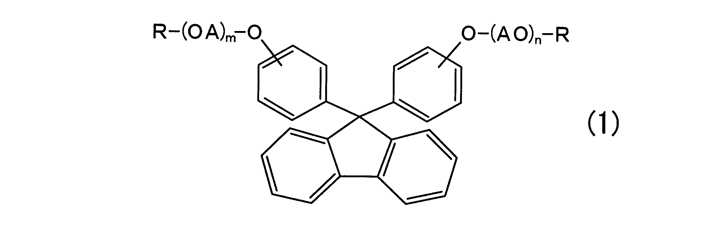
- Photopolymerization initiator In the formula, R represents an acryloyl group, a methacryloyl group or a vinyl group, A represents an alkylene group, and m and n each independently represents an integer of 0 to 3.
- the film produced from the imprint material and having the pattern transferred thereon has a low dielectric constant and a high transmittance. And having a high refractive index.
- the imprint material of the present invention can be photocured, and the cured film does not peel off part of the pattern when the mold is released, so that a film in which a desired pattern is accurately formed can be obtained. . Therefore, it is possible to form a good optical imprint pattern.
- the imprint material of the present invention can be formed on an arbitrary substrate, and the film to which the pattern formed after imprint is transferred is not only an optical member but also a semiconductor element such as a field effect transistor. It can be suitably used for the interlayer insulating film and / or the gate insulating film. Furthermore, the imprint material of this invention can control a cure rate, dynamic viscosity, and a film thickness by changing the kind of compound which has at least 2 polymeric group in a molecule
- the present invention is characterized in that a compound having a bisarylfluorene skeleton is used as a monomer, and a film having a low dielectric constant is imparted to a film formed from an imprint material containing the compound. That is, an imprint containing (A) a component having a bisarylfluorene skeleton, (B) a component having at least one polymerizable group in the molecule, and (C) a photopolymerization initiator. Material. Furthermore, in addition to the component (A), the component (B), and the component (C), the imprint material can contain a solvent as the component (D).
- each component will be described in detail.
- the compound having a bisarylfluorene skeleton as the component (A) is represented by the following formula (1).
- R represents an acryloyl group, a methacryloyl group or a vinyl group
- A represents an alkylene group
- m and n each independently represents an integer of 0 to 3.
- the alkylene group is, for example, an alkylene group having 1 to 3 carbon atoms.
- the above m and n are 1, for example.
- the compound having a bisarylfluorene skeleton can be used as a monomer, and can impart a property of low dielectric constant to a film formed from an imprint material containing the compound.
- the above-mentioned compounds having a bisarylfluorene skeleton are available as commercial products. Specific examples thereof include OGSOL (registered trademark) EA-0200, EA-0500, EA-1000, EA-F5003, And EA-F5503 (Osaka Gas Chemical Co., Ltd.).
- the compounds having the bisarylfluorene skeleton can be used alone or in combination of two or more.
- the content of the component (A) in the imprint material of the present invention is preferably 50 to 95 parts by mass, more preferably 70 parts by mass, based on a total of 100 parts by mass of the component (A) and the component (B) described later. Or more. If this ratio is too small, the dielectric constant increases, making it difficult to obtain the desired physical properties.
- the “compound having at least one polymerizable group in the molecule” as the component (B) is a compound having at least one polymerizable group in one molecule and having the polymerizable group at the molecular end.
- the compound may be a monomer or an oligomer.
- the polymerizable group refers to at least one organic group selected from the group consisting of an acryloyloxy group, a methacryloyloxy group, a vinyl group, and an allyl group.
- the acryloyloxy group may be expressed as an acryloxy group
- the methacryloyloxy group may be expressed as a methacryloxy group.
- the number of the polymerizable groups in one molecule in the compound of the component (B) is generally 1 to 6, but may exceed 6.
- Examples of the compound having at least one polymerizable group as the component (B) include dipentaerythritol hexaacrylate, dipentaerythritol hexamethacrylate, dipentaerythritol pentaacrylate, dipentaerythritol pentamethacrylate, pentaerythritol tetraacrylate, Pentaerythritol triacrylate, pentaerythritol trimethacrylate, pentaerythritol diacrylate, pentaerythritol dimethacrylate, tetramethylolpropane tetraacrylate, tetramethylolpropane tetramethacrylate, tetramethylolmethane tetraacrylate, tetramethylolmethane tetramethacrylate, trimethylolpropane triacrylate, Trimethylo Propropane trimethacrylate,
- the above compounds are commercially available, and specific examples thereof include KAYARAD (registered trademark) T-1420, DPHA, DPHA-2C, D-310, D-330, and DPCA-20.
- the component (B) may be, for example, a mixture of a compound having 5 polymerizable groups and 6 compounds in one molecule. Therefore, the said compound can be used individually or in combination of 2 or more types.
- the component (B) plays a role in adjusting the viscosity of the compound having a bisarylfluorene skeleton, which is the component (A) having a high viscosity. Therefore, the content of the component (B) in the imprint material of the present invention is preferably 50 to 5 parts by mass, more preferably 10 based on the total of 100 parts by mass of the component (A) and the component (B). More than part by mass. If this proportion is excessive, the dielectric constant increases, while if this proportion is too small, the handleability deteriorates.
- ⁇ (C) component examples include tert-butylperoxy-iso-butarate, 2,5-dimethyl-2,5-bis (benzoyldioxy) hexane, 1,4-bis [ ⁇ - (Tert-butyldioxy) -iso-propoxy] benzene, di-tert-butyl peroxide, 2,5-dimethyl-2,5-bis (tert-butyldioxy) hexene hydroperoxide, ⁇ - (iso-propylphenyl) -iso- Propyl hydroperoxide, 2,5-dimethylhexane, tert-butyl hydroperoxide, 1,1-bis (tert-butyldioxy) -3,3,5-trimethylcyclohexane, butyl-4,4-bis (tert-butyldioxy) valerate , Cyclohexanone peroxide
- the above-mentioned compounds can be obtained as commercial products. Specific examples thereof include IRGACURE (registered trademark) 651, 184, 500, 2959, 127, 754, 907, 369, 379, 379EG, 819, 819DW, 1800, 1870, 784, OXE01, OXE02, 250, DAROCUR (registered trademark) 1173, MBF, TPO, 4265 (above, Ciba Japan Co., Ltd.) KAYACURE (registered trademark) DETX, MBP, DMBI, EPA, OA (above, Nippon Kayaku Co., Ltd.), VISURE-10, 55 (above, STAUFFER Co.
- the above photopolymerization initiators can be used alone or in combination of two or more.
- the content of the component (C) in the imprint material of the present invention is preferably 0.5 phr to 30 phr, and preferably 1 phr to 20 phr with respect to the total mass of the component (A) and the component (B). It is more preferable. When this ratio is 0.1 phr or less, sufficient curability cannot be obtained and patterning characteristics deteriorate.
- phr represents the mass of the photopolymerization initiator with respect to 100 g of the total mass of the components (A) and (B).
- a solvent may be contained as the component (D).
- the solvent as the component (D) plays a role in adjusting the viscosity of the compound having the bisarylfluorene skeleton as the component (A).
- solvent examples include toluene, p-xylene, o-xylene, styrene, ethylene glycol dimethyl ether, propylene glycol monomethyl ether, ethylene glycol monomethyl ether, propylene glycol, propylene glycol monoethyl ether, ethylene glycol monoethyl ether, ethylene glycol.
- Monoisopropyl ether ethylene glycol methyl ether acetate, propylene glycol monomethyl ether acetate, ethylene glycol ethyl ether acetate, diethylene glycol dimethyl ether, propylene glycol monobutyl ether, ethylene glycol monobutyl ether, diethylene glycol diethyl ether, dipropylene glycol monomethyl ether Diethylene glycol monomethyl ether, dipropylene glycol monoethyl ether, diethylene glycol monoethyl ether, triethylene glycol dimethyl ether, diethylene glycol monoethyl ether acetate, diethylene glycol, 1-octanol, ethylene glycol, hexylene glycol, diacetone alcohol, furfuryl alcohol, tetrahydrofur Furyl alcohol, propylene glycol, benzyl alcohol, 1,3-butanediol, 1,4-butanediol, 2,3-butanediol,
- the solvent is preferably propylene glycol monomethyl ether acetate, propylene Glycol monomethyl ether, ⁇ -butyrolactone, N-methylpyrrolidone, methanol, ethanol, isopropanol, butanol, diacetone alcohol, acetone, methyl ethyl ketone, methyl isobutyl ketone, ethylene glycol, propylene glycol, hexylene glycol, methyl cellosolve, ethylene cellosolve, butyl cellosolve , Ethyl carbitol, butyl carbitol, diethylene glycol monomethyl ether, propylene glycol monomethyl ether, pro Glycol monobutyl ether, cyclohexanone, methyl acetate,
- the above solvents can be used alone or in combination of two or more.
- the imprint material of the present invention can contain a photosensitizer, an ultraviolet absorber, an antioxidant, a surfactant, an adhesion aid, and the like as necessary as long as the effects of the present invention are not impaired. .
- photosensitizer examples include, for example, thioxanthene series, xanthene series, ketone series, thiopyrylium salt series, base styryl series, merocyanine series, 3-substituted coumarin series, 3,4-substituted coumarin series, cyanine series, acridine series. , Thiazine, phenothiazine, anthracene, coronene, benzanthracene, perylene, ketocoumarin, fumarine, borate and the like.
- the above photosensitizers can be used alone or in combination of two or more.
- the wavelength in the UV region can also be adjusted by using the photosensitizer.
- Examples of the ultraviolet absorber include TINUVIN (registered trademark) PS, 99-2, 109, 328, 384-2, 400, 405, 460, 477, 479, 900, 928, 1130, 111FDL, 123, 144, 152, 292, 5100, 400-DW, 477-DW, 99-DW, 123-DW, 5050, 5060, 5151 (Ciba Japan Co., Ltd.) and the like.
- TINUVIN registered trademark
- PS 99-2, 109, 328, 384-2
- 400 405, 460, 477, 479, 900, 928, 1130, 111FDL, 123, 144, 152, 292, 5100, 400-DW, 477-DW, 99-DW, 123-DW, 5050, 5060, 5151 (Ciba Japan Co., Ltd.) and the like.
- the above ultraviolet absorbers can be used alone or in combination of two or more. By using the ultraviolet absorber, it is possible to control the curing speed of the outermost surface of the film during photocuring and to improve the mold release property.
- antioxidants examples include IRGANOX (registered trademark) 1010, 1035, 1076, 1135, 1520L (above, Ciba Japan Co., Ltd.) and the like.
- the above antioxidants can be used alone or in combination of two or more. By using the antioxidant, it is possible to prevent the film from turning yellow due to oxidation.
- surfactant examples include polyoxyethylene lauryl ether, polyoxyethylene stearyl ether, polyoxyethylene acetyl ether, polyoxyethylene alkyl ethers such as polyoxyethylene olein ether, polyoxyethylene octylphenol ether, polyoxyethylene Nonielphenol ethers polyoxyethylene alkyl allyl ethers, polyoxyethylene / polyoxypropylene block copolymers, sorbitan monolaurate, sorbitan monopalmitate, sorbitan monostearate, sorbitan monooleate, sorbitan trioleate, sorbitan Sorbitan fatty acid esters such as tristearate, polyoxyethylene sorbitan monolaurate, polyoxy Nonionic surfactants such as polyoxyethylene sorbitan fatty acid esters, such as Tylene sorbitan monopalmitate, polyoxyethylene sorbitan monostearate, polyoxyethylene sorbitan trioleate, polyoxyethylene sorbitan tristearate
- the above surfactants can be used alone or in combination of two or more.
- the ratio is preferably 0.01 phr to 10 phr, more preferably 0.01 phr to 5 phr, with respect to the total mass of the component (A) and the component (B).
- adhesion aid examples include 3-methacryloxypropyltrimethoxysilane, 3-acryloxypropyltrimethoxysilane, and the like. By using the adhesion aid, the adhesion with the substrate is improved.
- the content of the adhesion aid is preferably 5 phr to 50 phr, more preferably 10 phr to 50 phr, with respect to the total mass of the component (A) and the component (B).
- the method for preparing the imprint material of the present invention is not particularly limited as long as the component (A), the component (B), the component (C), and the component (D) are uniformly mixed. Further, the order of mixing the components (A) to (D) is not particularly limited as long as a uniform solution can be obtained.
- the preparation method include a method of mixing the component (B) and the component (C) in a predetermined ratio with the component (A). Moreover, the method etc. which further mix (D) component with this and make it a uniform solution are mentioned. Furthermore, in an appropriate stage of this preparation method, there may be mentioned a method in which other additives are further added and mixed as necessary.
- the solvent which is the component (D) it may be fired for the purpose of evaporating the solvent with respect to at least one of the film before light irradiation and the film after light irradiation.
- the baking equipment is not particularly limited. For example, it can be fired in a suitable atmosphere, that is, in an inert gas such as air or nitrogen, in a vacuum, using a hot plate, an oven, or a furnace. I just need it.
- the firing temperature is not particularly limited for the purpose of evaporating the solvent, but can be performed at 40 to 200 ° C., for example.
- the imprint material of the present invention can be applied to a substrate, photocured, and then heated as necessary to obtain a desired film.
- a coating method a known or well-known method such as a spin coating method, a dip method, a flow coating method, an ink jet method, a spray method, a bar coating method, a gravure coating method, a slit coating method, a roll coating method, a transfer printing method, Examples thereof include brush coating, blade coating, and air knife coating.
- Examples of the base material on which the imprint material of the present invention is applied include silicon, glass on which indium tin oxide (ITO) is formed (hereinafter abbreviated as “ITO substrate”), and silicon nitride (SiN). And a substrate made of indium zinc oxide (IZO), polyethylene terephthalate (PET), plastic, glass, quartz, ceramics, and the like. It is also possible to use a flexible base material having flexibility.
- ITO substrate glass on which indium tin oxide
- SiN silicon nitride
- IZO indium zinc oxide
- PET polyethylene terephthalate
- plastic glass, quartz, ceramics, and the like. It is also possible to use a flexible base material having flexibility.
- a light source for curing the imprintable material of the present invention is not particularly limited, for example, a high pressure mercury lamp, low pressure mercury lamp, a metal halide lamp, KrF excimer laser, ArF excimer laser, F 2 excimer laser, electron beam (EB), And extreme ultraviolet (EUV).
- a 436 nm G line, a 405 nm H line, a 365 nm I line, or a GHI mixed line can be used.
- the exposure dose is preferably 30 to 2000 mJ / cm 2 , more preferably 30 to 1000 mJ / cm 2 .
- the optical imprinting apparatus is not particularly limited as long as a target pattern can be obtained.
- ST50 manufactured by Toshiba Machine Co., Ltd.
- Sindre registered trademark
- NM-0801HB manufactured by Meisho Agency, etc.
- a commercially available apparatus can be used.
- Examples of the mold material used for optical imprinting used in the present invention include quartz, silicon, nickel, carbonylsilane, glassy carbon and the like, but are not particularly limited as long as a target pattern can be obtained. Further, the mold may be subjected to a mold release treatment for forming a thin film such as a fluorine compound on the surface thereof in order to improve the mold release property. Examples of the mold release agent used for the mold release treatment include OPTOOL (registered trademark) HD manufactured by Daikin Industries, Ltd., but are not particularly limited as long as the target pattern can be obtained.
- a pattern suitable for the target electronic device may be selected, and the pattern size conforms to this.
- the pattern size is, for example, nanometer order and micrometer order.
- Ogsol registered trademark
- EA-0200 Osaka Gas Chemical Co., Ltd.
- NPGDA neopentyl glycol diacrylate
- IRGACURE registered trademark
- OXE01 manufactured by Ciba Japan Co., Ltd.
- Example 2 An imprint material PNI-2 was prepared in the same manner except that NPGDA in Example 1 was changed to pentaerythritol triacrylate (manufactured by Aldrich) (hereinafter abbreviated as “PTA”).
- PTA pentaerythritol triacrylate
- Example 3 13.1 g of propylene glycol monomethyl ether acetate (hereinafter abbreviated as “PGMEA”) was added to PNI-1 obtained in Example 1 to prepare imprint material PNI-3.
- PGMEA propylene glycol monomethyl ether acetate
- Imprint material PNI-4 was prepared by adding 13.1 g of PGMEA to PNI-2 obtained in Example 2.
- Imprint material PNI-a was prepared by adding 0.5 g of OXE01 (5 phr with respect to NPGDA) to 10 g of NPGDA.
- Imprint material PNI-d was prepared by adding 10.5 g of PGEMA to PNI-a obtained in Comparative Example 1.
- Imprint material PNI-f was prepared by adding 10.5 g of PGEMA to PNI-c obtained in Comparative Example 3.
- the PNI-2 obtained in Example 2 was spin-coated on a quartz substrate to obtain a film for optical imprint (PNI-2F).
- the PNI-3 obtained in Example 3 was spin-coated on a quartz substrate and pre-baked for 1 minute on a hot plate at 100 ° C. to obtain a film for photoimprinting (PNI-3F).
- the PNI-4 obtained in Example 4 was spin-coated on a quartz substrate and pre-baked for 1 minute on a hot plate at 100 ° C. to obtain a film for photoimprinting (PNI-4F).
- the PNI-a obtained in Comparative Example 1 was spin-coated on a quartz substrate to obtain a film for optical imprint (PNI-aF).
- the PNI-b obtained in Comparative Example 2 was spin-coated on a quartz substrate to obtain a film for optical imprint (PNI-bF).
- the PNI-c obtained in Comparative Example 3 was spin-coated on a quartz substrate to obtain a film for optical imprint (PNI-cF).
- the PNI-d obtained in Comparative Example 4 was spin-coated on a quartz substrate and pre-baked for 1 minute on a hot plate at 100 ° C. to obtain a film for photoimprinting (PNI-dF).
- the PNI-e obtained in Comparative Example 5 was spin-coated on a quartz substrate and pre-baked for 1 minute on a hot plate at 100 ° C. to obtain a film for photoimprinting (PNI-eF).
- the PNI-f obtained in Comparative Example 6 was spin-coated on a quartz substrate and pre-baked for 1 minute on a hot plate at 100 ° C. to obtain a film for photoimprinting (PNI-fF).
- NM-0801HB manufactured by Meisho Agency
- NM-0801HB manufactured by Meisho Agency
- Each of the coating films for optical imprint obtained in Examples 1 to 4 and Comparative Examples 1 to 6 was subjected to a patterning test.
- the mold used was made of silicon, and the pattern was 120 nm line and space.
- the mold is immersed in Optool (registered trademark) HD (manufactured by Daikin Industries, Ltd.) in advance, treated for 2 hours using a high-temperature and high-humidity device with a temperature of 90 ° C and a humidity of 90RH%, rinsed with pure water, What was dried with was used.
- Optool registered trademark
- HD manufactured by Daikin Industries, Ltd.
- the silicon mold was adhered to the PNI-1F produced from the PNI-1 obtained in Example 1 and installed in the optical imprint apparatus.
- Optical imprinting is always performed at 23 ° C. under conditions of a) pressurization to 1000 N over 10 seconds, b) exposure at 500 mJ / cm 2 using a high-pressure mercury lamp, c) pressure removal over 10 seconds, d) mold And the substrate were separated and released.
- the results of optical imprint are shown in Table 1.
- photocuring refers to the evaluation of whether the film is cured after exposure, “ ⁇ ” indicates curing, and “x” indicates that curing has not occurred.
- Bond refers to an evaluation of whether or not a part of the pattern is peeled off from the mold at the time of mold release, “ ⁇ ” indicates that peeling has not occurred, and “ ⁇ ” indicates that peeling has been observed.
- Shape refers to an evaluation of whether or not the mold pattern has been successfully transferred to the film after release, and “ ⁇ ” indicates that the film has been transferred well, and “x” indicates that the film has not been transferred well.
- composition of the imprint material forming the low dielectric constant film capable of good photoimprinting is as follows: (A) component: compound having a bisarylfluorene skeleton represented by the above formula (1), ( It became clear that the component (B): a compound having at least two polymerizable groups in the molecule and the component (C): a photopolymerization initiator are essential. Furthermore, it became clear that (D) component: a solvent may be contained.
- the dielectric constant was measured using a vacuum simple prober MJ-10 (manufactured by Major Jig Co., Ltd.) and AG-4411B LCR meter (manufactured by Ando Electric Co., Ltd.) at a frequency of 100 kHz.
- the PNI-1 obtained in Example 1 was spin-coated on an ITO substrate, and a quartz substrate was placed on the ITO substrate.
- the pressure was constantly increased to 1000 N over 10 seconds under the condition of 23 ° C., and b) a high-pressure mercury lamp was used.
- a photocured film was formed on the ITO substrate in a sequence of exposure of 500 mJ / cm 2 , c) pressure removal over 10 seconds, and d) separation of the quartz substrate and the ITO substrate, and part of the film. was removed to expose the ITO.
- the dielectric constant was measured in the same manner as described above except that PNI-2 obtained in Example 2 was used. The results are shown in Table 2.
- the PNI-3 obtained in Example 3 was spin-coated on an ITO substrate, calcined for 1 minute on a 100 ° C. hot plate, and covered with a quartz substrate on the condition of 23 ° C. a) for 10 seconds.
- ITO substrate in a sequence of pressurizing up to 1000 N, b) exposure at 500 mJ / cm 2 using a high-pressure mercury lamp, c) pressure removal over 10 seconds, d) separation of the quartz substrate and the ITO substrate and release.
- a photocured film was prepared on top and baked on a hot plate at 200 ° C. for 1 minute. A part of the film was scraped to expose the ITO.
- the dielectric constant was measured in the same manner as described above except that PNI-4 obtained in Example 4 was used instead of PNI-3. The results are shown in Table 2.
- the PNI-a obtained in Comparative Example 1 was spin-coated on an ITO substrate, and a quartz substrate was placed on the ITO substrate, and a) pressurized to 1000 N over 10 seconds under the condition of 23 ° C., b) a high-pressure mercury lamp.
- a photocured film was formed on the ITO substrate in a sequence of exposure of 500 mJ / cm 2 , c) pressure removal over 10 seconds, and d) separation of the quartz substrate and the ITO substrate, and part of the film. was removed to expose the ITO.
- the dielectric constant was measured in the same manner as described above except that PNI-b obtained in Comparative Example 2 was used. The results are shown in Table 2.
- the dielectric constant was measured in the same manner as described above except that PNI-c obtained in Comparative Example 3 was used. The results are shown in Table 2.
- the PNI-d obtained in Comparative Example 4 was spin coated on an ITO substrate, pre-baked on a hot plate at 100 ° C. for 1 minute, and covered with a quartz substrate on the condition of 23 ° C. a) for 10 seconds.
- ITO substrate in a sequence of pressurizing up to 1000 N, b) exposure at 500 mJ / cm 2 using a high-pressure mercury lamp, c) pressure removal over 10 seconds, d) separation of the quartz substrate and the ITO substrate and release.
- a photocured film was prepared on top and baked on a hot plate at 200 ° C. for 1 minute. A part of the film was scraped to expose the ITO.
- the dielectric constant was measured in the same manner as described above except that PNI-e obtained in Comparative Example 5 was used instead of PNI-d. The results are shown in Table 2.
- the dielectric constant was measured in the same manner as described above except that PNI-f obtained in Comparative Example 6 was used instead of PNI-d. The results are shown in Table 2.
- the PNI-1 obtained in Example 1 was spin-coated on a quartz substrate, and another quartz substrate was put on the quartz substrate, and the pressure was constantly increased to 1000 N over 10 seconds under the condition of 23 ° C.
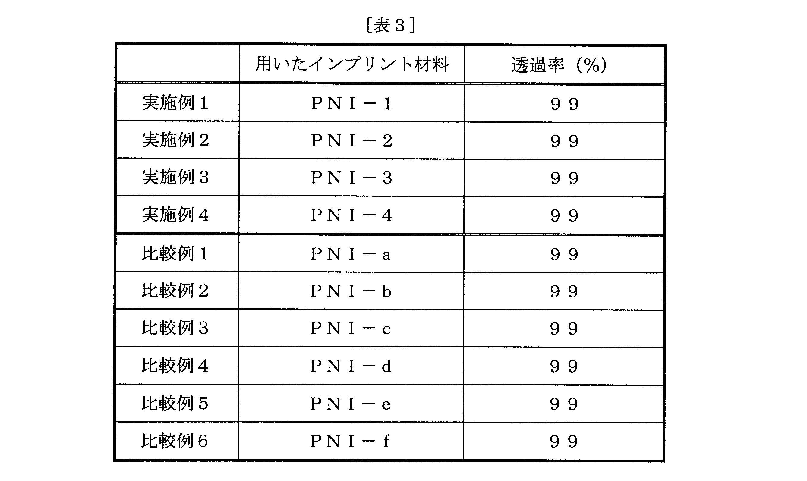
- a photocured film was prepared on a quartz substrate in the same manner as described above except that PNI-2 obtained in Example 2 was used, and the transmittance was measured. The results are shown in Table 3.
- the PNI-3 obtained in Example 3 was spin-coated on a quartz substrate and pre-baked for 1 minute on a hot plate at 100 ° C. Then, it is covered with another quartz substrate, and a) pressurized to 1000 N over 10 seconds under the condition of 23 ° C., b) exposure at 500 mJ / cm 2 using a high-pressure mercury lamp, c) pressure removal over 10 seconds, d) After the covered quartz substrate is separated from the lower quartz substrate and released, a photocured film is produced on the quartz substrate and baked on a hot plate at 200 ° C., and the transmittance is measured. went. The results are shown in Table 3.
- a photocured film was prepared on a quartz substrate in the same manner as above except that PNI-4 obtained in Example 4 was used instead of PNI-3, and the transmittance was measured. The results are shown in Table 3.
- PNI-a obtained in Comparative Example 1 is spin-coated on a quartz substrate, and another quartz substrate is covered on the quartz substrate, and a) pressurized to 1000 N over 10 seconds under the condition of 23 ° C. b) high-pressure mercury A photocured film is formed on the quartz substrate in a sequence of exposure at 500 mJ / cm 2 using a lamp, c) pressure removal over 10 seconds, and d) separation of the covered quartz substrate from the lower quartz substrate and release. It produced and the transmittance
- a photocured film was prepared on a quartz substrate in the same manner as described above except that PNI-b obtained in Comparative Example 2 was used, and the transmittance was measured. The results are shown in Table 3.
- a photocured film was prepared on a quartz substrate in the same manner as described above except that PNI-c obtained in Comparative Example 3 was used, and the transmittance was measured. The results are shown in Table 3.
- the PNI-d obtained in Comparative Example 4 was spin-coated on a quartz substrate and pre-baked for 1 minute on a hot plate at 100 ° C. Then, it is covered with another quartz substrate, and a) pressurized to 1000 N over 10 seconds under the condition of 23 ° C., b) exposure at 500 mJ / cm 2 using a high-pressure mercury lamp, c) pressure removal over 10 seconds, d) After the covered quartz substrate is separated from the lower quartz substrate and released, a photocured film is produced on the quartz substrate and baked on a hot plate at 200 ° C., and the transmittance is measured. went. The results are shown in Table 3.
- a photocured film was prepared on a quartz substrate in the same manner as above except that PNI-e obtained in Comparative Example 5 was used instead of PNI-d, and the transmittance was measured. The results are shown in Table 3.
- a photocured film was prepared on a quartz substrate in the same manner as described above except that PNI-f obtained in Comparative Example 6 was used instead of PNI-d, and the transmittance was measured. The results are shown in Table 3.
- the PNI-1 obtained in Example 1 was spin-coated on a silicon wafer, and a quartz substrate was placed on the silicon wafer, and a) pressurized to 1000 N over 10 seconds under the condition of 23 ° C., b) a high-pressure mercury lamp.
- a photocured film is produced on the silicon wafer in the sequence of exposure at 500 mJ / cm 2 , c) pressure removal over 10 seconds, and d) separation of the quartz substrate and the silicon wafer, and refractive index measurement. went.
- the results are shown in Table 4.
- a photocured film was prepared on a silicon wafer in the same manner as described above except that PNI-2 obtained in Example 2 was used, and the refractive index was measured. The results are shown in Table 4.
- PNI-3 obtained in Example 3 was spin-coated on a silicon wafer and pre-baked for 1 minute on a hot plate at 100 ° C. Then, a quartz substrate is put on the substrate, and the pressure is constantly increased to 1000 N for 10 seconds under conditions of 23 ° C., b) exposure at 500 mJ / cm 2 using a high-pressure mercury lamp, and c) pressure removal for 10 seconds. D) A photocured film was prepared on a silicon wafer in a sequence of separating and releasing the quartz substrate and the silicon wafer and firing on a hot plate at 200 ° C., and then the refractive index was measured. The results are shown in Table 4.
- a photocured film was prepared on a silicon wafer in the same manner as above except that PNI-4 obtained in Example 4 was used instead of PNI-3, and the refractive index was measured. The results are shown in Table 4.
- the PNI-a obtained in Comparative Example 1 was spin-coated on a silicon wafer, and a quartz substrate was put on the silicon wafer, and the pressure was constantly increased to 1000 N for 10 seconds under the condition of 23 ° C., and b) a high-pressure mercury lamp was used.
- a photocured film is produced on the silicon wafer in the sequence of exposure at 500 mJ / cm 2 , c) pressure removal over 10 seconds, and d) separation of the quartz substrate and the silicon wafer, and refractive index measurement. went.
- the results are shown in Table 4.
- a photocured film was prepared on a silicon wafer in the same manner as described above except that the PNI-b obtained in Comparative Example 2 was used, and the refractive index was measured. The results are shown in Table 4.
- a photocured film was prepared on a silicon wafer in the same manner as above except that PNI-c obtained in Comparative Example 3 was used, and the refractive index was measured. The results are shown in Table 4.
- the PNI-d obtained in Comparative Example 4 was spin-coated on a silicon wafer and pre-baked for 1 minute on a hot plate at 100 ° C. Then, a quartz substrate is put on the substrate, and the pressure is constantly increased to 1000 N for 10 seconds under conditions of 23 ° C., b) exposure at 500 mJ / cm 2 using a high-pressure mercury lamp, and c) pressure removal for 10 seconds. D) A photocured film was prepared on a silicon wafer in a sequence of separating and releasing the quartz substrate and the silicon wafer, and baked on a hot plate at 200 ° C., and then the refractive index was measured. The results are shown in Table 4.
- a photocured film was prepared on a silicon wafer in the same manner as above except that PNI-e obtained in Comparative Example 5 was used instead of PNI-d, and the refractive index was measured. The results are shown in Table 4.
- a photocured film was prepared on a silicon wafer in the same manner as described above except that PNI-f obtained in Comparative Example 6 was used instead of PNI-d, and the refractive index was measured. The results are shown in Table 4.
- the film obtained from the imprint material of the present invention has good optical imprint properties and has a low dielectric constant, a high refractive index, and a high transmittance.
- the film obtained from the imprint material of the present invention can be suitably used for electronic devices and optical members such as interlayer insulating films and / or gate insulating films of semiconductor elements such as field effect transistors.
Landscapes
- Engineering & Computer Science (AREA)
- Physics & Mathematics (AREA)
- Nanotechnology (AREA)
- Chemical & Material Sciences (AREA)
- General Physics & Mathematics (AREA)
- Crystallography & Structural Chemistry (AREA)
- Theoretical Computer Science (AREA)
- Condensed Matter Physics & Semiconductors (AREA)
- Mathematical Physics (AREA)
- Manufacturing & Machinery (AREA)
- Spectroscopy & Molecular Physics (AREA)
- Exposure Of Semiconductors, Excluding Electron Or Ion Beam Exposure (AREA)
- Shaping Of Tube Ends By Bending Or Straightening (AREA)
- Addition Polymer Or Copolymer, Post-Treatments, Or Chemical Modifications (AREA)
Abstract
Description
したがって、ナノインプリントリソグラフィは、光リソグラフィ技術に代わり、半導体デバイス、オプトデバイス、ディスプレイ、記憶媒体、バイオチップ等の製造への適用が期待されている技術である。このことから、ナノインプリントリソグラフィに用いる光ナノインプリントリソグラフィ用硬化性組成物について様々な報告がなされている(特許文献2、3)。
ここで、上述より、本発明の課題は、高透過率、高屈折率及び低誘電率を有する膜を形成するインプリント材料を提供することである。具体的には、透過率については、例えば、95%以上、好ましくは98%以上の高い透過率を有する膜を形成する材料の提供を目的とし、屈折率については、例えば、1.57以上、好ましくは1.60以上の高い屈折率を有する膜を形成する材料の提供を目的とし、誘電率については、例えば、2.0以上3.2以下、好ましくは3.0以下の低い誘電率を有する膜を形成する材料の提供を目的とする。
とりわけ、本発明の特徴は、透過率、屈折率及び誘電率等の諸特性について全て満足する性能を有する膜を形成するインプリント材料を提供することにある。
また、本明細書では、形成されるパターンサイズがナノメートルオーダーに限らず、例えば、マイクロメートルオーダーである場合を含む光ナノインプリント技術を光インプリントと称する。さらに、本明細書では、“誘電率”とは比誘電率を意味する。
すなわち、本発明は、
(A)成分、(B)成分、及び(C)成分を含有し、前記(A)成分及び前記(B)成分の合計100質量部に基づいて、50乃至95質量部の(A)成分、及び50乃至5質量部の(B)成分をそれぞれ含有するインプリント材料。
(A)成分:下記式(1)で表されるビスアリールフルオレン骨格を有する化合物
(B)成分:分子内に少なくとも1個の重合性基を有する化合物
(C)成分:光重合開始剤
本発明のインプリント材料は、光硬化が可能であり、かつその硬化膜は、モールドの離型時にパターンの一部の剥がれが生じないため、所望のパターンが正確に形成された膜が得られる。したがって、良好な光インプリントのパターン形成が可能である。
また、本発明のインプリント材料は、任意の基材上に成膜することができ、インプリント後に形成されるパターンが転写された膜は、光学部材だけでなく、電界効果トランジスタ等の半導体素子の層間絶縁膜及び/又はゲート絶縁膜に好適に用いることができる。
さらに、本発明のインプリント材料は、分子内に少なくとも2個の重合性基を有する化合物の種類を変更することで、硬化速度、動的粘度、膜厚をコントロールすることができる。したがって、本発明のインプリント材料は、製造するデバイス種と露光プロセス及び焼成プロセスの種類に対応した材料の設計が可能であり、プロセスマージンを拡大できるため、光学部材の製造に好適に用いることができる。
以下、各成分について詳細に説明する。
(A)成分であるビスアリールフルオレン骨格を有する化合物は、下記式(1)で表される。

(B)成分の「分子内に少なくとも1個の重合性基を有する化合物」とは、一分子中に重合性基を1個以上有し、かつ該重合性基が分子末端にある化合物のことを表す。そして、当該化合物は単量体であるか、又はオリゴマーであってもよい。また、当該重合性基としては、例えば、アクリロイルオキシ基、メタアクリロイルオキシ基、ビニル基及びアリル基からなる群から選ばれる少なくとも1種類の有機基のことを指す。ここで、アクリロイルオキシ基はアクリロキシ基と、メタアクリロイルオキシ基はメタアクリロキシ基と表現されることがある。また、(B)成分の化合物における一分子中の当該重合性基の数は、一般的には1個乃至6個であるが、6個を超えても良い。
したがって、本発明のインプリント材料における(B)成分の含有量は、上記(A)成分及び上記(B)成分の合計100質量部に基づいて、好ましくは50乃至5質量部、より好ましくは10質量部以上である。この割合が過大である場合には、誘電率は増大し、一方、この割合が過少である場合には、ハンドリング性が悪化する。
(C)成分である光重合開始剤としては、例えば、tert-ブチルペルオキシ-iso-ブタレート、2,5-ジメチル-2,5-ビス(ベンゾイルジオキシ)ヘキサン、1,4-ビス[α-(tert-ブチルジオキシ)-iso-プロポキシ]ベンゼン、ジ-tert-ブチルペルオキシド、2,5-ジメチル-2,5-ビス(tert-ブチルジオキシ)ヘキセンヒドロペルオキシド、α-(iso-プロピルフェニル)-iso-プロピルヒドロペルオキシド、2,5-ジメチルヘキサン、tert-ブチルヒドロペルオキシド、1,1-ビス(tert-ブチルジオキシ)-3,3,5-トリメチルシクロヘキサン、ブチル-4,4-ビス(tert-ブチルジオキシ)バレレート、シクロヘキサノンペルオキシド、2,2’,5,5’-テトラ(tert-ブチルペルオキシカルボニル)ベンゾフェノン、3,3’,4,4’-テトラ(tert-ブチルペルオキシカルボニル)ベンゾフェノン、3,3’,4,4’-テトラ(tert-アミルペルオキシカルボニル)ベンゾフェノン、3,3’,4,4’-テトラ(tert-ヘキシルペルオキシカルボニル)ベンゾフェノン、3,3’-ビス(tert-ブチルペルオキシカルボニル)-4,4’-ジカルボキシベンゾフェノン、tert-ブチルペルオキシベンゾエート、ジ-tert-ブチルジペルオキシイソフタレート等の有機過酸化物や、9,10-アントラキノン、1-クロロアントラキノン、2-クロロアントラキノン、オクタメチルアントラキノン、1,2-ベンズアントラキノン等のキノン類や、ベンゾインメチル、ベンゾインエチルエーテル、α-メチルベンゾイン、α-フェニルベンゾイン等のベンゾイン誘導体、2,2-ジメトキシ-1,2-ジフェニルエタン-1-オン、1-ヒドロキシ-シクロヘキシル-フェニル-ケトン、2-ヒドロキシ-2-メチル-1-フェニル-プロパン-1-オン、1-[4-(2-ヒドロキシエトキシ)-フェニル]-2-ヒドロキシ-2-メチル-1-プロパン-1-オン、2-ヒドロキシ-1-[4-{4-(2-ヒドロキシ-2-メチル-プロピオニル)ベンジル}-フェニル]-2-メチル-プロパン-1-オン、フェニルグリオキシリックアシッドメチルエステル、2-メチル-1-[4-(メチルチオ)フェニル]-2-モルフォリノプロパン-1-オン、2-ベンジル-2-ジメチルアミノ-1-(4-モルフォリノフェニル)-ブタノン-1、2-ジメチルアミノ-2-(4-メチル-ベンジル)-1-(4-モリフォリン-4-イル-フェニル)-ブタン-1-オン、ビス(2,4,6-トリメチルベンゾイル)-フェニルフォスフィンオキサイド、2,4,6-トリメチルベンゾイル-ジフェニル-フォスフィンオキサイド、1,2-オクタンジオン,1-[4-(フェニルチオ)-,2-(o-ベンゾイルオキシム)]、エタノン,1-[9-エチル-6-(2-メチルベンゾイル)-9H-カルバゾール-3-イル]-,1-(o-アセチルオキシム)等が挙げられるが、光硬化時に使用する光源に吸収をもつものであれば、特に限定されるものではない。
本発明においては(D)成分として溶剤を含有しても良い。
(D)成分である溶剤は、(A)成分であるビスアリールフルオレン骨格を有する化合物の粘度調節の役割を果たす。
<実施例1>
オグソール(登録商標)EA-0200(大阪ガスケミカル株式会社製)(以下、「オグソール」と略す) 10gにKAYARAD(登録商標)ネオペンチルグリコールジアクリレート(日本化薬株式会社製)(以下、「NPGDA」と略す)を2.5g(オグソール100質量部に対して25質量部)、IRGACURE(登録商標)OXE01(チバ・ジャパン株式会社製)(以下、「OXE01」と略す)を0.62g(オグソール及びNPGDAの総質量に対して5phr)を加え、インプリント材料PNI-1を調製した。
実施例1のNPGDAをペンタエリスリトールトリアクリレート(アルドリッチ社製)(以下、「PTA」と略す)に変更した以外は同様にインプリント材料PNI-2を調製した。
実施例1で得られたPNI-1にプロピレングリコールモノメチルエーテルアセテート(以下、「PGMEA」と略す)を13.1g加えてインプリント材料PNI-3を調製した。
実施例2で得られたPNI-2にPGMEAを13.1g加えてインプリント材料PNI-4を調製した。
NPGDA 10gにOXE01 0.5g(NPGDAに対して5phr)を加えてインプリント材料PNI-aを調製した。
比較例1のNPGDAをPTAに変更した以外は同様にインプリント材料PNI-bを調製した。
実施例1のオグソールをPTAに変更した以外は同様にインプリント材料PNI-cを調製した。
比較例1で得られたPNI-aにPGEMAを10.5g加えてインプリント材料PNI-dを調製した。
比較例2で得られたPNI-bにPGEMAを10.5g加えてインプリント材料PNI-eを調製した。
比較例3で得られたPNI-cにPGEMAを10.5g加えてインプリント材料PNI-fを調製した。
実施例1で得たPNI-1を石英基板上にスピンコートし、光インプリント用被膜(PNI-1F)を得た。
ナノインプリント装置は、NM-0801HB(明昌機構株式会社製)を使用した。
実施例1乃至実施例4並びに比較例1乃至比較例6で得られた各光インプリント用被膜をパターニング試験した。用いたモールドはシリコン製であり、パターンは120nmのラインアンドスペースとした。モールドは事前にオプツール(登録商標)HD(ダイキン工業株式会社製)に浸漬し、温度が90℃、湿度が90RH%の高温高湿装置を用いて2時間処理し、純水でリンス後、エアーで乾燥させたものを使用した。

誘電率測定は、真空簡易プローバMJ-10((株)メジャージグ製)及びAG-4311B LCRメータ(安藤電機(株)製)を使用し、周波数100kHzで測定を行った。
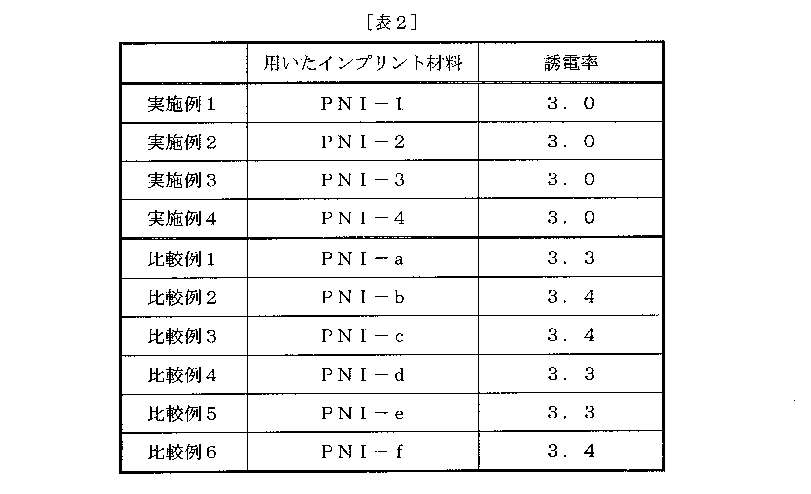
以上の結果から、本発明のインプリント材料により得られる膜は、3.0以下の低誘電率を有するものとなる。
透過率測定は、UV-2550 UV-VISIBLE SPECTROPHOTOMETER(株式会社島津製作所製)を使用し、波長400nmにおけるサンプル膜厚1μmでの透過率を算出した。
屈折率測定は、n&k Technology 1512RT(n&k Technology, Inc製)を使用し、波長633nmの屈折率を測定した。

以上の結果から、本発明のインプリント材料により得られる膜は、1.6を超える高屈折率を有するものとなる。
Claims (8)
- (A)成分、(B)成分、及び(C)成分を含有し、前記(A)成分及び前記(B)成分の合計100質量部に基づいて、50乃至95質量部の(A)成分、及び50乃至5質量部の(B)成分をそれぞれ含有するインプリント材料。
(A)成分:下記式(1)で表されるビスアリールフルオレン骨格を有する化合物
(B)成分:分子内に少なくとも1個の重合性基を有する化合物
(C)成分:光重合開始剤

- 更に(D)成分として溶剤を含有する、請求項1に記載のインプリント材料。
- 前記(A)成分及び前記(B)成分の合計100質量部に基づいて、70質量部以上の前記(A)成分を含有する、請求項1に記載のインプリント材料。
- 前記(B)成分は重合性基として、アクリロイルオキシ基、メタアクリロイルオキシ基、ビニル基及びアリル基からなる群から選ばれる少なくとも1種の基を有する化合物であることを特徴とする、請求項1乃至請求項3のうちいずれか一項に記載のインプリント材料。
- 請求項1乃至請求項4のうちいずれか一項に記載のインプリント材料から作製され、パターンが転写された膜。
- 請求項5に記載のパターンが転写された膜を基材上に備えた光学部材。
- 請求項5に記載のパターンが転写された膜を備えた半導体素子。
- 請求項5に記載のパターンが転写された膜を備えた電子デバイス。
Priority Applications (1)
| Application Number | Priority Date | Filing Date | Title |
|---|---|---|---|
| JP2011519713A JP5348433B2 (ja) | 2009-06-19 | 2010-05-31 | 低誘電率インプリント材料 |
Applications Claiming Priority (2)
| Application Number | Priority Date | Filing Date | Title |
|---|---|---|---|
| JP2009146354 | 2009-06-19 | ||
| JP2009-146354 | 2009-06-19 |
Publications (1)
| Publication Number | Publication Date |
|---|---|
| WO2010146983A1 true WO2010146983A1 (ja) | 2010-12-23 |
Family
ID=43356303
Family Applications (1)
| Application Number | Title | Priority Date | Filing Date |
|---|---|---|---|
| PCT/JP2010/059187 Ceased WO2010146983A1 (ja) | 2009-06-19 | 2010-05-31 | 低誘電率インプリント材料 |
Country Status (4)
| Country | Link |
|---|---|
| JP (1) | JP5348433B2 (ja) |
| KR (1) | KR101560249B1 (ja) |
| TW (1) | TWI475029B (ja) |
| WO (1) | WO2010146983A1 (ja) |
Cited By (6)
| Publication number | Priority date | Publication date | Assignee | Title |
|---|---|---|---|---|
| JP2012224845A (ja) * | 2011-04-08 | 2012-11-15 | Osaka Gas Chem Kk | 硬化性組成物およびその硬化物 |
| KR20140077889A (ko) * | 2011-09-27 | 2014-06-24 | 마루젠 세끼유가가꾸 가부시키가이샤 | 광학 소자 재료, 및 그 제조 방법 |
| TWI553408B (zh) * | 2011-09-30 | 2016-10-11 | 富士軟片股份有限公司 | 奈米壓印方法以及用於該奈米壓印方法的抗蝕劑組成物 |
| JP2017212394A (ja) * | 2016-05-27 | 2017-11-30 | Jsr株式会社 | インプリント用感放射線性組成物及びパターン |
| CN107710385A (zh) * | 2015-06-29 | 2018-02-16 | 日产化学工业株式会社 | 压印材料 |
| US10295901B2 (en) | 2013-06-06 | 2019-05-21 | Dic Corporation | Curable composition for imprinting |
Families Citing this family (4)
| Publication number | Priority date | Publication date | Assignee | Title |
|---|---|---|---|---|
| JP6170288B2 (ja) | 2012-09-11 | 2017-07-26 | 富士フイルム株式会社 | 転写材料、静電容量型入力装置の製造方法および静電容量型入力装置、並びに、これを備えた画像表示装置 |
| JP6327947B2 (ja) | 2013-06-26 | 2018-05-23 | キヤノン株式会社 | 光硬化性組成物、これを用いた、膜の製造方法、光学部品の製造方法、回路基板の製造方法、電子部品の製造方法、硬化物 |
| JP6327948B2 (ja) | 2013-06-26 | 2018-05-23 | キヤノン株式会社 | 光硬化性組成物、硬化物、これを用いた、膜の製造方法、光学部品の製造方法、回路基板の製造方法、電子部品の製造方法 |
| JP6494185B2 (ja) | 2013-06-26 | 2019-04-03 | キヤノン株式会社 | インプリント方法および装置 |
Citations (4)
| Publication number | Priority date | Publication date | Assignee | Title |
|---|---|---|---|---|
| JP2005010231A (ja) * | 2003-06-16 | 2005-01-13 | Dainippon Printing Co Ltd | 凹凸パターン形成材料、凹凸パターン受容体、凹凸パターン形成方法、転写箔、及び光学物品 |
| JP2009031764A (ja) * | 2007-07-04 | 2009-02-12 | Mitsubishi Rayon Co Ltd | 反射防止物品、およびこれより得られる成形品、ならびにこれらを備えた自動車用部品 |
| WO2009145061A1 (ja) * | 2008-05-29 | 2009-12-03 | 旭硝子株式会社 | 光硬化性組成物および表面に微細パターンを有する成形体の製造方法 |
| JP2010001419A (ja) * | 2008-06-23 | 2010-01-07 | Alps Electric Co Ltd | Uvナノインプリント成型体及びその製造方法 |
Family Cites Families (4)
| Publication number | Priority date | Publication date | Assignee | Title |
|---|---|---|---|---|
| JP3797223B2 (ja) * | 1999-11-29 | 2006-07-12 | オムロン株式会社 | 耐光性マイクロレンズアレイおよびそれに使用する樹脂組成物 |
| JP4756977B2 (ja) * | 2005-09-28 | 2011-08-24 | 大阪瓦斯株式会社 | 重合性組成物およびその硬化物 |
| JP2007291321A (ja) * | 2006-03-27 | 2007-11-08 | Sanyo Electric Co Ltd | 硬化型有機金属組成物及び有機金属ポリマー材料並びに光学部品 |
| JP2009051017A (ja) | 2007-08-23 | 2009-03-12 | Fujifilm Corp | 光ナノインプリントリソグラフィ用光硬化性組成物、及びパターン付き基板の製造方法 |
-
2010
- 2010-05-31 JP JP2011519713A patent/JP5348433B2/ja active Active
- 2010-05-31 KR KR1020127001224A patent/KR101560249B1/ko active Active
- 2010-05-31 WO PCT/JP2010/059187 patent/WO2010146983A1/ja not_active Ceased
- 2010-06-10 TW TW099118932A patent/TWI475029B/zh active
Patent Citations (4)
| Publication number | Priority date | Publication date | Assignee | Title |
|---|---|---|---|---|
| JP2005010231A (ja) * | 2003-06-16 | 2005-01-13 | Dainippon Printing Co Ltd | 凹凸パターン形成材料、凹凸パターン受容体、凹凸パターン形成方法、転写箔、及び光学物品 |
| JP2009031764A (ja) * | 2007-07-04 | 2009-02-12 | Mitsubishi Rayon Co Ltd | 反射防止物品、およびこれより得られる成形品、ならびにこれらを備えた自動車用部品 |
| WO2009145061A1 (ja) * | 2008-05-29 | 2009-12-03 | 旭硝子株式会社 | 光硬化性組成物および表面に微細パターンを有する成形体の製造方法 |
| JP2010001419A (ja) * | 2008-06-23 | 2010-01-07 | Alps Electric Co Ltd | Uvナノインプリント成型体及びその製造方法 |
Cited By (7)
| Publication number | Priority date | Publication date | Assignee | Title |
|---|---|---|---|---|
| JP2012224845A (ja) * | 2011-04-08 | 2012-11-15 | Osaka Gas Chem Kk | 硬化性組成物およびその硬化物 |
| KR20140077889A (ko) * | 2011-09-27 | 2014-06-24 | 마루젠 세끼유가가꾸 가부시키가이샤 | 광학 소자 재료, 및 그 제조 방법 |
| KR101864920B1 (ko) * | 2011-09-27 | 2018-06-05 | 마루젠 세끼유가가꾸 가부시키가이샤 | 광학 소자 재료, 및 그 제조 방법 |
| TWI553408B (zh) * | 2011-09-30 | 2016-10-11 | 富士軟片股份有限公司 | 奈米壓印方法以及用於該奈米壓印方法的抗蝕劑組成物 |
| US10295901B2 (en) | 2013-06-06 | 2019-05-21 | Dic Corporation | Curable composition for imprinting |
| CN107710385A (zh) * | 2015-06-29 | 2018-02-16 | 日产化学工业株式会社 | 压印材料 |
| JP2017212394A (ja) * | 2016-05-27 | 2017-11-30 | Jsr株式会社 | インプリント用感放射線性組成物及びパターン |
Also Published As
| Publication number | Publication date |
|---|---|
| JP5348433B2 (ja) | 2013-11-20 |
| KR20120034105A (ko) | 2012-04-09 |
| JPWO2010146983A1 (ja) | 2012-12-06 |
| KR101560249B1 (ko) | 2015-10-14 |
| TW201120061A (en) | 2011-06-16 |
| TWI475029B (zh) | 2015-03-01 |
Similar Documents
| Publication | Publication Date | Title |
|---|---|---|
| JP5348433B2 (ja) | 低誘電率インプリント材料 | |
| JP6319596B2 (ja) | 高耐擦傷性インプリント材料 | |
| JP5263560B2 (ja) | 高硬度インプリント材料 | |
| JP6429031B2 (ja) | シルセスキオキサン化合物及び変性シリコーン化合物を含むインプリント材料 | |
| JP5445743B2 (ja) | 光インプリント用被膜形成用組成物 | |
| US9533467B2 (en) | Imprint material having low mold release property | |
| CN103329246B (zh) | 含有氨基甲酸酯化合物的高耐擦伤性压印材料 | |
| JP2013095833A (ja) | 高屈折率インプリント材料 | |
| JP5794420B2 (ja) | シリコーン骨格を有する化合物を含む光インプリント材料 | |
| CN109563194B (zh) | 压印材料 | |
| CN106575606A (zh) | 压印材料 | |
| KR20180021725A (ko) | 임프린트 재료 |
Legal Events
| Date | Code | Title | Description |
|---|---|---|---|
| 121 | Ep: the epo has been informed by wipo that ep was designated in this application |
Ref document number: 10789358 Country of ref document: EP Kind code of ref document: A1 |
|
| WWE | Wipo information: entry into national phase |
Ref document number: 2011519713 Country of ref document: JP |
|
| NENP | Non-entry into the national phase |
Ref country code: DE |
|
| ENP | Entry into the national phase |
Ref document number: 20127001224 Country of ref document: KR Kind code of ref document: A |
|
| 122 | Ep: pct application non-entry in european phase |
Ref document number: 10789358 Country of ref document: EP Kind code of ref document: A1 |