WO2010146913A1 - Dispositif d'éclairage, dispositif d'affichage et récepteur de télévision - Google Patents
Dispositif d'éclairage, dispositif d'affichage et récepteur de télévision Download PDFInfo
- Publication number
- WO2010146913A1 WO2010146913A1 PCT/JP2010/056204 JP2010056204W WO2010146913A1 WO 2010146913 A1 WO2010146913 A1 WO 2010146913A1 JP 2010056204 W JP2010056204 W JP 2010056204W WO 2010146913 A1 WO2010146913 A1 WO 2010146913A1
- Authority
- WO
- WIPO (PCT)
- Prior art keywords
- chassis
- light source
- holding member
- main body
- led
- Prior art date
Links
Images


Classifications
-
- G—PHYSICS
- G02—OPTICS
- G02F—OPTICAL DEVICES OR ARRANGEMENTS FOR THE CONTROL OF LIGHT BY MODIFICATION OF THE OPTICAL PROPERTIES OF THE MEDIA OF THE ELEMENTS INVOLVED THEREIN; NON-LINEAR OPTICS; FREQUENCY-CHANGING OF LIGHT; OPTICAL LOGIC ELEMENTS; OPTICAL ANALOGUE/DIGITAL CONVERTERS
- G02F1/00—Devices or arrangements for the control of the intensity, colour, phase, polarisation or direction of light arriving from an independent light source, e.g. switching, gating or modulating; Non-linear optics
- G02F1/01—Devices or arrangements for the control of the intensity, colour, phase, polarisation or direction of light arriving from an independent light source, e.g. switching, gating or modulating; Non-linear optics for the control of the intensity, phase, polarisation or colour
- G02F1/13—Devices or arrangements for the control of the intensity, colour, phase, polarisation or direction of light arriving from an independent light source, e.g. switching, gating or modulating; Non-linear optics for the control of the intensity, phase, polarisation or colour based on liquid crystals, e.g. single liquid crystal display cells
- G02F1/133—Constructional arrangements; Operation of liquid crystal cells; Circuit arrangements
- G02F1/1333—Constructional arrangements; Manufacturing methods
- G02F1/1335—Structural association of cells with optical devices, e.g. polarisers or reflectors
- G02F1/1336—Illuminating devices
- G02F1/133602—Direct backlight
- G02F1/133608—Direct backlight including particular frames or supporting means
-
- G—PHYSICS
- G02—OPTICS
- G02F—OPTICAL DEVICES OR ARRANGEMENTS FOR THE CONTROL OF LIGHT BY MODIFICATION OF THE OPTICAL PROPERTIES OF THE MEDIA OF THE ELEMENTS INVOLVED THEREIN; NON-LINEAR OPTICS; FREQUENCY-CHANGING OF LIGHT; OPTICAL LOGIC ELEMENTS; OPTICAL ANALOGUE/DIGITAL CONVERTERS
- G02F2201/00—Constructional arrangements not provided for in groups G02F1/00 - G02F7/00
- G02F2201/46—Fixing elements
- G02F2201/465—Snap -fit
Definitions
- the present invention relates to a lighting device, a display device, and a television receiver.
- a backlight device is separately required as a lighting device.
- the backlight device is installed on the back side of the liquid crystal panel (the side opposite to the display surface).
- the chassis has an open surface on the liquid crystal panel side, a light source accommodated in the chassis, A reflection sheet that is disposed along the inner surface and reflects light toward the opening of the chassis, and an optical member that is disposed at the opening of the chassis and efficiently emits light emitted from the light source toward the liquid crystal panel (a diffusion sheet) Etc.).
- an LED may be used as a light source.
- an LED substrate on which the LED is mounted is accommodated in the chassis.
- what was described in following patent document 1 is known as an example of the backlight apparatus which used LED as a light source.
- the LED substrate disposed in the chassis may be fixed to the chassis with a screw together with the reflection sheet. At this time, if the LED substrate and the reflection sheet are fixed at multiple locations with screws, the following problems may occur.
- the LED substrate and the reflection sheet may expand or contract due to thermal expansion or contraction.
- the LED substrate and the reflection sheet are firmly fixed at a number of locations by screws, expansion and contraction is restricted at the fixed portion, so local deformation such as warpage and deflection at the non-fixed portion. It was easy to occur.
- the above-described deformation occurs in the reflection sheet, unevenness is easily generated in the reflected light, which may adversely affect the display quality.
- the above-described deformation occurs in the LED substrate, a contact failure occurs at a connection point with an external circuit or the like, and there is a possibility that a problem occurs when performing lighting control of the LED or the like.
- the present invention has been completed based on the above circumstances, and an object thereof is to make it difficult for local deformation to occur in the extending member.
- the illumination device includes a light source, a chassis that houses the light source, an extending member that extends along an inner surface of the chassis, and the chassis in a state where the extending member is sandwiched between the chassis.
- the holding member is provided with an abutting portion that protrudes toward the extending member and abuts against the extending member.
- the extending member is held in a state of being sandwiched between the holding member and the chassis.
- the holding member is provided with an abutting portion that protrudes toward the extending member, and the abutting portion abuts against the extending member, so that the surface of the holding member that faces the extending member extends over the entire area.
- the contact area of the holding member with respect to the extending member can be reduced compared to the case where the holding member is in contact with the extending member. In other words, in the extending member, the area of the portion that is not in contact with the holding member and cannot be pressed by the holding member increases.
- This unpressed portion is more easily expanded and contracted when thermal expansion or contraction occurs due to changes in the thermal environment, compared to the portion pressed by the holding member. And if the area of this non-pressed part becomes large, since the freedom degree of expansion / contraction as a whole extending member will increase, it will suppress that deformation, such as bending and warp accompanying expansion and contraction, becomes locally obvious. be able to.
- the extending member may be easily slipped with respect to the contact portion (contact portion) of the holding member when the extending member is thermally expanded or contracted. It may be possible to increase the degree of freedom of expansion and contraction of the extending member.
- the holding member includes a main body part that sandwiches the extending member with the chassis, and a fixing part that protrudes from the main body part toward the chassis side and is fixed to the chassis. Is provided in the main body. In this way, when the fixing portion is fixed to the chassis, the extending member sandwiched between the main body portion and the chassis is suitably held. At this time, the abutting portion abuts on the extending member, and the entire surface of the main body portion facing the extending member is avoided.
- the contact portion is disposed at a position away from the fixed portion in the main body portion.
- a pressing force acts on the extending member from both the chassis side and the main body side.
- the position where the pressing force acts from the chassis side and the position where the pressing force acts from the main body side depend on the positional relationship between the contact portion and the fixed portion.
- the contact portion is arranged at a position away from the fixed portion in the main body portion, the position where the pressing force acts from the chassis side and the position where the pressing force acts from the main body side on the extending member. Are shifted (offset) from each other when viewed in a plane.
- the stress acting on the extending member can be dispersed and the stress concentration can be reduced. be able to. Thereby, the freedom degree of the expansion-contraction in an extending member can be raised.
- the contact portion is disposed on an outer edge portion of the main body portion. If it does in this way, a holding member can be stably fixed to a chassis by arranging a fixed part in the center side in a main part. In addition, by arranging the contact part on the outer edge part of the main body part, the distance between the fixed part and the contact part can be ensured to the maximum, so that the stress concentration can be alleviated better and extended. The degree of freedom of expansion and contraction in the member can be further increased.
- the width can be increased, so that the degree of freedom of expansion and contraction in the extending member can be secured more stably.
- the fixed portion is disposed on the center side of the main body portion
- at least one pair of the contact portions is disposed at a position sandwiching the fixed portion in the main body portion. If it does in this way, a holding member can be stably fixed to a chassis by arranging a fixed part in the center side in a main part.
- the pressing force can be applied in a balanced manner to the extending member, and the degree of freedom of expansion and contraction of the extending member can be increased. It is possible to appropriately hold the extending member while raising it.
- the contact portion is disposed at a symmetrical position with the fixed portion as the center. In this way, the pressing force can be applied to the extending member in a more balanced manner.
- the contact portion is formed in an annular shape so as to surround the fixing portion. If it does in this way, a holding member can be stably fixed to a chassis by arranging a fixed part in the center side in a main part.
- the annular contact portion that surrounds the fixed portion is brought into contact with the extending member, the extending member can be more appropriately held in a balanced manner.
- the gap held between the main body portion and the extending member is surrounded by the annular contact portion, the gap is prevented from opening into the chassis. Therefore, it is possible to avoid light in the chassis from leaking into the gap. Furthermore, for example, when a gap is formed between the fixed portion and the chassis, it is possible to prevent light in the chassis from leaking out of the chassis through the gap.
- the contact portion is configured to be continuous with the fixed portion. If it does in this way, the intensity
- the contact portion is configured to surround the fixed portion. In this way, the strength of the contact part and the fixed part can be further improved.
- the fixing portion is fixed to the chassis while penetrating the extending member. If it does in this way, it will become possible to position an extending member about the direction which follows the plate surface by the fixed part which penetrates an extending member.
- the fixing portion penetrates the extending member and the chassis and is locked to the chassis from a side opposite to the extending member side.
- the holding member and the extending member can be fixed by locking the fixing portion penetrating the chassis together with the extending member to the chassis, and therefore other fixing means such as an adhesive is used. It is not necessary, and can be fixed easily at low cost.
- An optical member is disposed at a position facing the light source, and a support portion that protrudes toward the optical member and supports the optical member is provided on the main body. If it does in this way, the function to support an optical member can be given to the holding member which fixes an extending member together.
- the fixing portion and the support portion are arranged at positions that overlap each other when seen in a plane. In this way, when the operator attaches the holding member while gripping the support portion, the position of the fixed portion can be easily grasped, so that the workability is excellent.
- the fixed portion and the support portion are arranged at positions that are concentric with each other. In this way, workability is further improved.
- the abutting portion has a point-like shape when seen in a plane. In this way, the contact portion is brought into point contact with the extending member, so that the contact area can be reduced as much as possible, and the degree of freedom of expansion and contraction in the extending member can be increased.
- the contact portion is formed in a linear shape when seen in a plane. If it does in this way, since a contact part is line-contacted with respect to an extending member, an extending member can be hold
- the contact surface with respect to the said extending member is comprised by a curved surface. If it does in this way, an extending member becomes slippery with respect to a contact part, and the degree of freedom of expansion and contraction can be raised further.
- the said contact surface is comprised by the spherical surface. If it does in this way, an extending member becomes slippery more easily with respect to a contact part, and the freedom degree of expansion-contraction can be raised further.
- the extending member is a light source substrate having the light source. In this way, the degree of freedom of expansion and contraction associated with thermal expansion or contraction in the light source substrate is increased, so that contact failure is unlikely to occur at a connection location with an external circuit or the like, and lighting control of the light source is performed. It is possible to prevent a malfunction from occurring.
- a plurality of light sources are arranged in parallel on the light source substrate. If it does in this way, a plurality of light sources can be efficiently arranged to a light source substrate, and it becomes suitable for high brightness etc.
- the holding member is disposed between the adjacent light sources. In this way, the space held between adjacent light sources can be used effectively. Further, it is possible to prevent the holding member from obstructing the light emitted from the light source.
- the extending member is a reflecting member that reflects light from the light source. If it does in this way, light can be used effectively by reflecting light with a reflective member, and it becomes suitable for improvement of a brightness, etc. Since the degree of freedom of expansion and contraction associated with thermal expansion or contraction of the reflecting member is increased, unevenness is less likely to occur in the light reflected by the reflecting member.
- the extending member includes a light source substrate having the light source and a reflecting member that reflects light from the light source, and the light source substrate and the reflecting member are both stacked on each other. And the chassis. In this way, the light source substrate and the reflecting member can be collectively held by the holding member. In addition, the degree of freedom of expansion and contraction accompanying thermal expansion or contraction in the light source substrate and the reflecting member is increased.
- the reflection member is disposed on a side opposite to the chassis side with respect to the light source substrate, and has a light source insertion hole through which the light source passes at a position overlapping the light source when seen in a plan view. ing. If it does in this way, light can be used more effectively by reflecting light with the reflective member arranged on the opposite side to the chassis side to a light source board, and it becomes suitable for an improvement in brightness, etc. . Moreover, since the reflection member has the light source insertion hole, it is avoided that the emission of light from the light source is hindered.
- a diffusion lens that diffuses light from the light source is disposed at a position overlapping the light source when viewed in plan. In this way, the light emitted from the light source can be emitted after being diffused by the diffusion lens. Thereby, unevenness is less likely to occur in the emitted light.
- the reflection member is interposed between the first reflection member having a size that allows the light source insertion hole to pass the diffusion lens, and the light source substrate and the diffusion lens, and viewed in a plane. And a second reflecting member that is disposed at a position overlapping the light source insertion hole provided in the first reflecting member and reflects light toward the diffuser lens. In this way, even if a light source insertion hole having a size for allowing the diffusion lens to pass through is provided in the first reflection member, the light is diffused by the second reflection member disposed at a position overlapping the light source insertion hole. Can be reflected to the side. As a result, light can be used effectively, which is suitable for improving luminance.
- the edge of the light source insertion hole in the first reflecting member and the second reflecting member are formed so as to overlap each other when seen in a plan view. If it does in this way, the edge part of the light source penetration hole in the 1st reflective member and the 2nd reflective member will be connected seamlessly seeing in a plane. Thereby, light can be utilized more effectively.
- a restricting portion for restricting a positional relationship of the holding member with respect to the extending member is provided so that a gap is held between the holding member and the extending member. According to this configuration, since the holding member is restricted in positional relation to the extending member by the restricting portion, a gap is held between the holding member and the extending member, so that the extending member is thermally expanded or contracted. It becomes easy to expand and contract with this.
- the degree of freedom of expansion and contraction in the extending member can be kept high as compared with the case where the surface of the member facing the extending member is in contact with the extending member over the entire area.
- the holding member includes a main body portion that sandwiches the light source substrate with the chassis, and a fixing portion that protrudes from the main body portion toward the chassis and is fixed to the chassis.
- a second part that is attached to the first part and restricts elastic deformation of the elastic locking piece.
- a display device of the present invention includes the above-described illumination device and a display panel that performs display using light from the illumination device.
- the lighting device that supplies light to the display panel is difficult to cause local deformation in the extending member that extends along the inner surface of the chassis. Unevenness does not easily occur in the light reflected and emitted by the member, so that it is possible to realize display with excellent display quality.
- a liquid crystal panel can be exemplified as the display panel.
- Such a display device can be applied as a liquid crystal display device to various uses such as a display of a television or a personal computer, and is particularly suitable for a large screen.
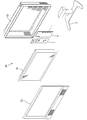
- FIG. 1 is an exploded perspective view showing a schematic configuration of a television receiver according to Embodiment 1 of the present invention.
- the exploded perspective view which shows schematic structure of the liquid crystal display device with which a television receiver is equipped
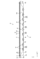
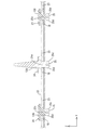
- the top view which shows the arrangement configuration of the LED board and holding member in the chassis with which a liquid crystal display device is equipped.
- FIG. 3 is a cross-sectional view taken along the line v-v in FIG.
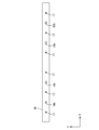
- the top view which shows the detailed arrangement structure of a LED board and a holding member Vii-vii sectional view of FIG. Viii-viii sectional view of FIG. Sectional view taken along line ix-ix in FIG.
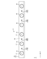
- Plan view of LED board The top view which shows the state (light source unit) which attached the 2nd reflective sheet and the diffusion lens to the LED board.
- Plan view of single-function holding member Bottom view of single-function holding member
- Plan view of multifunctional holding member Bottom view of multifunctional holding member Sectional view taken along line ix-ix in FIG. 6 showing a state before the holding member is attached to the chassis.
- 6 is a cross-sectional view taken along the line ix-ix in FIG. 6 showing a state in which the main body is elastically deformed with the holding member attached to the chassis.
- the bottom view which shows the holding member which concerns on the modification 1 of Embodiment 1.
- Sectional drawing which shows the state before attaching a holding member to a chassis Sectional drawing which shows the state which attached the holding member to the chassis Sectional drawing which shows the state which attached the holding member which concerns on the modification 2 of Embodiment 1 to the chassis.
- Sectional drawing which shows the state which the contact part contact
- Sectional drawing which shows the state which attached the holding member to the chassis Sectional drawing which shows the state which attached the holding member which concerns on the modification 1 of Embodiment 2 to the chassis.
- Sectional drawing which shows the state which attached the holding member which concerns on the modification 2 of Embodiment 2 to the chassis. Sectional drawing which shows the state before attaching the holding member which concerns on Embodiment 3 of this invention to a chassis. Sectional drawing which shows the state which attached the 1st component among the holding members to the chassis. Sectional drawing which shows the state which mounted
- FIGS. 1 A first embodiment of the present invention will be described with reference to FIGS.
- the liquid crystal display device 10 is illustrated.
- a part of each drawing shows an X axis, a Y axis, and a Z axis, and each axis direction is drawn to be a direction shown in each drawing.
- the upper side shown in FIG.4 and FIG.5 be a front side, and let the lower side of the figure be a back side.
- the television receiver TV includes a liquid crystal display device 10, front and back cabinets Ca and Cb that are accommodated so as to sandwich the liquid crystal display device 10, a power source P, a tuner T, And a stand S.
- the liquid crystal display device (display device) 10 has a horizontally long rectangular shape (rectangular shape) as a whole and is accommodated in a vertically placed state.
- the liquid crystal display device 10 includes a liquid crystal panel 11 that is a display panel and a backlight device (illumination device) 12 that is an external light source, which are integrated by a frame-like bezel 13 or the like. Is supposed to be retained.
- the screen size is 42 inches and the aspect ratio is 16: 9.
- the liquid crystal panel 11 and the backlight device 12 constituting the liquid crystal display device 10 will be described sequentially.
- the liquid crystal panel (display panel) 11 has a rectangular shape in plan view, and a pair of glass substrates are bonded together with a predetermined gap therebetween, and liquid crystal is sealed between the glass substrates. It is said.
- One glass substrate is provided with a switching element (for example, TFT) connected to a source wiring and a gate wiring orthogonal to each other, a pixel electrode connected to the switching element, an alignment film, and the like.
- the substrate is provided with a color filter and counter electrodes in which colored portions such as R (red), G (green), and B (blue) are arranged in a predetermined arrangement, and an alignment film.
- a polarizing plate is disposed on the outside of both substrates.
- the backlight device 12 covers the chassis 14 having a substantially box shape having an opening 14 b on the light emitting surface side (the liquid crystal panel 11 side), and the opening 14 b of the chassis 14.
- a group of optical members 15 (diffusion plate (light diffusion member) 15a and a plurality of optical sheets 15b arranged between the diffusion plate 15a and the liquid crystal panel 11), and an optical member disposed along the outer edge of the chassis 14.
- a frame 16 that holds the outer edge portion of the group of members 15 between the chassis 14 and the chassis 14.
- an LED 17 Light Emitting Diode
- an LED board 18 extending member on which the LED 17 is mounted
- an LED board 18 extending member on which the LED 17 is mounted
- an LED board 18 extending member on which the LED 17 is mounted
- a diffusing lens 19 attached at a position corresponding to the LED 17.
- a holding member 20 that can hold the LED substrate 18 between the chassis 14 and a reflection sheet 21 (extending member) that reflects the light in the chassis 14 toward the optical member 15.
- the optical member 15 side is the light emission side from the LED 17.
- the chassis 14 is made of metal and, as shown in FIGS. 3 to 5, has a rectangular bottom plate 14a similar to the liquid crystal panel 11, a side plate 14c rising from an outer end of each side of the bottom plate 14a, and each side plate 14c. And a receiving plate 14d projecting outward from the rising edge, and as a whole, has a shallow substantially box shape (substantially shallow dish shape) opened toward the front side.
- the long side direction of the chassis 14 coincides with the X-axis direction (horizontal direction), and the short side direction coincides with the Y-axis direction (vertical direction).
- a frame 16 and an optical member 15 to be described below can be placed on each receiving plate 14d in the chassis 14 from the front side.
- a frame 16 is screwed to each receiving plate 14d.
- An attachment hole 14e for attaching the holding member 20 is provided in the bottom plate 14a of the chassis 14 so as to open.
- a plurality of mounting holes 14e are dispersedly arranged corresponding to the mounting position of the holding
- the optical member 15 has a horizontally long rectangular shape (rectangular shape) in a plan view, like the liquid crystal panel 11 and the chassis 14. As shown in FIGS. 4 and 5, the optical member 15 has its outer edge portion placed on the receiving plate 14 d so as to cover the opening 14 b of the chassis 14 and be interposed between the liquid crystal panel 11 and the LED 17. Arranged.
- the optical member 15 includes a diffusion plate 15a disposed on the back side (the side opposite to the LED 17 side and the light emitting side) and an optical sheet 15b disposed on the front side (the liquid crystal panel 11 side and the light emitting side). .
- the diffusing plate 15a has a structure in which a large number of diffusing particles are dispersed in a substantially transparent resin base material having a predetermined thickness, and has a function of diffusing transmitted light.
- the optical sheet 15b has a sheet shape that is thinner than the diffusion plate 15a, and two optical sheets 15b are stacked (FIGS. 7 to 9). Specific types of the optical sheet 15b include, for example, a diffusion sheet, a lens sheet, a reflective polarizing sheet, and the like, which can be appropriately selected and used.
- the frame 16 has a frame shape along the outer peripheral edge portions of the liquid crystal panel 11 and the optical member 15. An outer edge portion of the optical member 15 can be sandwiched between the frame 16 and each receiving plate 14d (FIGS. 4 and 5).
- the frame 16 can receive the outer edge portion of the liquid crystal panel 11 from the back side, and can sandwich the outer edge portion of the liquid crystal panel 11 with the bezel 13 disposed on the front side (FIGS. 4 and 5). ).
- the LED 17 has a configuration in which an LED chip is sealed with a resin material on a substrate portion fixed to the LED substrate 18.
- the LED chip mounted on the substrate unit has one main emission wavelength, and specifically, one that emits blue light in a single color is used.
- a phosphor that converts blue light emitted from the LED chip into white light is dispersed and blended in the resin material for sealing the LED chip.
- the LED 17 can emit white light.
- the LED 17 is a so-called top type in which a surface opposite to the mounting surface with respect to the LED substrate 18 is a light emitting surface 17a.
- the optical axis LA of the LED 17 is set to substantially coincide with the Z-axis direction (direction orthogonal to the main plate surfaces of the liquid crystal panel 11 and the optical member 15). Note that the light emitted from the LED 17 spreads radially to some extent within a predetermined angle range around the optical axis LA, but its directivity is higher than that of a cold cathode tube or the like. In other words, the light emission intensity of the LED 17 shows an angular distribution in which the direction along the optical axis LA is remarkably high and decreases rapidly as the tilt angle with respect to the optical axis LA increases.
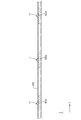
- the LED substrate 18 has a base material that has a rectangular shape in plan view, and the long side direction matches the X-axis direction, and the short side direction matches the Y-axis direction.
- the base material of the LED substrate 18 is made of a metal such as the same aluminum material as that of the chassis 14, and a wiring pattern made of a metal film such as a copper foil is formed on the surface thereof via an insulating layer.
- insulating materials such as a ceramic, can also be used as a ceramic.
- the surface facing the front side (the surface facing the optical member 15 side) has the above-described configuration as shown in FIGS.
- the LED 17 is surface mounted.
- a plurality of LEDs 17 are linearly arranged in parallel along the long side direction (X-axis direction) of the LED substrate 18, and are connected in series by a wiring pattern formed on the LED substrate 18.
- the arrangement pitch of the LEDs 17 is substantially constant, that is, it can be said that the LEDs 17 are arranged at equal intervals.
- the connector part 18a is provided in the both ends of the long side direction in the LED board 18. As shown in FIG.
- the LED substrate 18 having the above-described configuration is arranged in parallel in the chassis 14 in a state where the long side direction and the short side direction are aligned with each other in the X-axis direction and the Y-axis direction. ing. That is, the LED board 18 and the LED 17 mounted thereon are both set in the X-axis direction (the long side direction of the chassis 14 and the LED board 18) in the chassis 14 and in the Y-axis direction (of the chassis 14 and the LED board 18). Matrix arrangement (arranged in a matrix) with the short side direction as the column direction.
- a total of 27 LED substrates 18 are arranged in parallel in the chassis 14, three in the X-axis direction and nine in the Y-axis direction.
- two types of LED substrates 18 having different long side dimensions and the number of LEDs 17 to be mounted are used.
- the LED substrate 18 six LEDs 17 are mounted, and the long side dimension is a relatively long six-part mounting type and the five LEDs 17 are mounted, and the long side dimension is relatively long.
- the short five-mount type is used, one for the six-mount type at the X-axis direction end position of the chassis 14 and one for the five-mount type at the central position in the same direction. , Each is arranged.
- the LED boards 18 that form one row along the X-axis direction are electrically connected to each other by fitting and connecting the adjacent connector portions 18a to each other.
- Connector portions 18a corresponding to both ends in the X-axis direction are electrically connected to external control circuits (not shown).
- the LEDs 17 arranged on the LED boards 18 in one row are connected in series, and the lighting / extinction of a large number of LEDs 17 included in the row is collectively controlled by a single control circuit. Therefore, it is possible to reduce the cost.
- the short side dimension and the arrangement pitch of LED17 are made substantially the same.
- each liquid crystal display device 10 having a screen size of, for example, 26 inches, 32 inches, 37 inches, 40 inches, 42 inches, 46 inches, 52 inches, and 65 inches is used. Therefore, it is possible to easily cope with the manufacture at a low cost.
- the diffusing lens 19 is made of a synthetic resin material (for example, polycarbonate or acrylic) that is almost transparent (having high translucency) and has a refractive index higher than that of air. As shown in FIGS. 7, 8, and 11, the diffusing lens 19 has a predetermined thickness and is formed in a substantially circular shape when seen in a plan view, and each LED 17 is individually connected to the LED substrate 18 from the front side. So as to cover each LED 17 in a plan view. The diffusing lens 19 can emit light having strong directivity emitted from the LED 17 while diffusing.
- a synthetic resin material for example, polycarbonate or acrylic
- the diffusing lens 19 is disposed at a position that is substantially concentric with the LED 17 in a plan view.
- the diffuser lens 19 is sufficiently larger in both the X-axis direction and the Y-axis direction than the LED 17.
- the diffusing lens 19 has a smaller dimension in the X-axis direction than the LED board 18 but a larger dimension in the Y-axis direction than the LED board 18. Accordingly, both end portions of the diffusing lens 19 in the Y-axis direction protrude outward from the LED substrate 18 by a predetermined dimension in the Y-axis direction.
- the surface facing the back side and facing the LED substrate 18 is a light incident surface 19 a on which light from the LED 17 is incident, whereas the surface facing the front side and facing the optical member 15 is the surface facing the optical member 15.
- the light exit surface 19b emits light.
- the light incident surface 19 a is formed in parallel with the plate surface (X-axis direction and Y-axis direction) of the LED substrate 18 as a whole.
- the light incident side concave portion 19c is formed in a region overlapping with the LED 17 when viewed, thereby having an inclined surface.
- the light incident side concave portion 19c has a substantially conical shape and is disposed at a substantially concentric position in the diffusing lens 19, and is open toward the back side, that is, the LED 17 side.
- the light incident side concave portion 19c has an opening end portion facing the LED 17 side having the largest diameter dimension and larger than the diameter dimension of the LED 17, and the diameter dimension gradually and gradually increases from there to the front side. It becomes smaller and is minimized at the front end.
- the light incident side concave portion 19c has a substantially inverted V-shaped cross section, and its peripheral surface is an inclined surface inclined with respect to the Z-axis direction. The inclined surface is inclined so that the front end thereof intersects the optical axis LA of the LED 17.
- the light emitted from the LED 17 and entering the light incident side concave portion 19c enters the diffusion lens 19 through the inclined surface, but at that time, the amount of the inclination angle of the inclined surface with respect to the optical axis LA is as follows.
- the light is refracted in a direction away from the center, that is, a wide angle, and enters the diffusing lens 19.
- the light projecting surface 19a protrudes toward the LED substrate 18 at a position radially outward from the light incident side concave portion 19c, and has a structure for attaching the diffusing lens 19 to the LED substrate 18.
- a mounting leg portion 19d is provided.
- Three attachment legs 19d are arranged in the diffuser lens 19 at positions closer to the outer peripheral end than the light incident side recess 19c, and the lines connecting the attachments form a substantially equilateral triangle when viewed in a plane. Arranged in position.
- Each attachment leg 19d can fix the diffusing lens 19 to the LED substrate 18 in an attached state by fixing the tip of the attachment leg 19d to the LED substrate 18 with an adhesive or the like.
- the diffusing lens 19 is fixed to the LED substrate 18 via the mounting leg portion 19d, so that a predetermined gap is formed between the light incident surface 19a and the LED substrate 18. In this gap, incidence of light from a space outside the diffusion lens 19 in a plan view is allowed. Further, in the attached state, the projecting tip portion of the LED 17 from the LED substrate 18 enters the light incident side recess 19c.
- the light exit surface 19b of the diffusion lens 19 is formed in a flat and substantially spherical shape.
- the light emitted from the diffusion lens 19 can be emitted while being refracted in a direction away from the center at the interface with the external air layer, that is, a wide angle.
- a light emitting side recess 19e is formed in a region of the light emitting surface 19b that overlaps the LED 17 when seen in a plan view.
- the light emitting side concave portion 19e has a substantially bowl shape, and is formed in a flat and substantially spherical shape with a peripheral surface having a downward slope toward the center.
- the angle formed by the tangent of the peripheral surface of the light exit side recess 19e with respect to the optical axis LA of the LED 17 is relatively larger than the angle formed by the inclined surface of the light incident side recess 19c with respect to the optical axis LA. It is said.
- the region of the light exit surface 19b that overlaps with the LED 17 when seen in a plane is a region where the amount of light from the LED 17 is extremely large compared to other regions, and the brightness tends to be locally high, but there
- the light emitting side recess 19e most of the light from the LED 17 can be emitted while being refracted at a wide angle, or a part of the light from the LED 17 can be reflected to the LED substrate 18 side. Thereby, it can suppress that the brightness
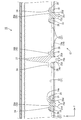
- the reflection sheet 21 includes a first reflection sheet 22 having a size covering the entire inner surface of the chassis 14 and a second reflection sheet 23 having a size covering each LED board 18 individually. Both the reflection sheets 22 and 23 are made of a synthetic resin, and the surfaces thereof are white with excellent light reflectivity. Both the reflection sheets 22 and 23 are assumed to extend along the bottom plate 14 a (LED substrate 18) in the chassis 14.
- the first reflection sheet 22 will be described.
- the body portion 22a is formed with a lens insertion hole 22b through which each diffusion lens 19 covering each LED 17 can be inserted together with each LED 17 arranged in the chassis 14.
- a plurality of lens insertion holes 22b are arranged in parallel at positions overlapping the respective LEDs 17 and the respective diffusion lenses 19 in a plan view in the main body portion 22a, and are arranged in a matrix.
- the lens insertion hole 22 b has a circular shape when seen in a plan view, and the diameter thereof is set to be larger than that of the diffusing lens 19.
- each diffusing lens 19 can be reliably passed through each lens insertion hole 22 b regardless of the occurrence of dimensional errors.
- the first reflection sheet 22 covers the area between the adjacent diffusion lenses 19 and the outer peripheral area in the chassis 14, so that the light toward each of the areas is directed toward the optical member 15. Can be reflected.
- the outer peripheral side portion of the first reflection sheet 22 rises so as to cover the side plate 14 c and the receiving plate 14 d of the chassis 14, and the portion placed on the receiving plate 14 d is the chassis 14.
- the optical member 15 Moreover, the part which connects the main-body part 22a and the part mounted on the receiving plate 14d among the 1st reflection sheets 22 has comprised the inclined form.
- the second reflection sheet 23 is formed in a rectangular shape as viewed in plan view, which is substantially the same outer shape as the LED substrate 18.
- the second reflection sheet 23 is disposed so as to overlap the front side surface of the LED substrate 18 and is opposed to the diffusion lens 19. That is, the second reflection sheet 23 is interposed between the diffusion lens 19 and the LED substrate 18. Therefore, about the light returned from the diffusion lens 19 side to the LED substrate 18 side, or the light entering the space between the diffusion lens 19 and the LED substrate 18 from the space outside the diffusion lens 19 in a plan view, The second reflection sheet 23 can again reflect the light toward the diffusing lens 19 side. As a result, the light utilization efficiency can be increased, and the luminance can be improved. In other words, sufficient brightness can be obtained even when the number of LEDs 17 is reduced to reduce the cost.
- the second reflection sheet 23 has a long side dimension substantially the same as that of the LED substrate 18, but a short side dimension larger than that of the LED substrate 18. Further, the short side dimension of the second reflecting sheet 23 is larger than the diameter dimension of the lens insertion hole 22b of the diffusing lens 19 and the first reflecting sheet 22, as shown in FIGS. Therefore, it is possible to arrange the edge of the lens insertion hole 22b in the first reflection sheet 22 so as to overlap the second reflection sheet 23 on the front side. As a result, the first reflection sheet 22 and the second reflection sheet 23 are continuously arranged in the chassis 14 without being interrupted when viewed in plan, and the chassis 14 or the LED board 18 is moved from the lens insertion hole 22b to the front side. There is almost no exposure.
- the light in the chassis 14 can be efficiently reflected toward the optical member 15, which is extremely suitable for improving the luminance.
- the second reflection sheet 23 penetrates through the positions where the LED insertion holes 23a through which the LEDs 17 pass and the leg insertion holes 23b through which the attachment legs 19d of the diffusing lenses 19 pass are overlapped with each other in plan view. Is formed.
- the holding member 20 has a combined function holding member 20B having a supporting function for supporting the optical member 15 in addition to a holding function for holding the LED substrate 18, and a single function having a holding function but not a supporting function.
- the mold holding member 20A There are two types, the mold holding member 20A.
- the suffix A is added to the symbol of the single-function type
- the suffix B is added to the symbol of the composite function type, and they are collectively referred to without distinction. No suffix is added to the code.
- a plurality of holding members 20 are arranged in parallel in the plane of the bottom plate 14 a of the chassis 14.
- the holding member 20 has a row direction in the X-axis direction (the longer side direction of the chassis 14 and the LED substrate 18) and a column direction in the Y-axis direction (the shorter side direction of the chassis 14 and the LED substrate 18) in the bottom plate 14a.
- a plurality are arranged in a matrix (arranged in a matrix).
- Each holding member 20 is disposed at a position overlapping each LED substrate 18 in a plan view and between adjacent diffusion lenses 19 (LEDs 17).
- the holding members 20 are arranged in the same arrangement as the diffusion lens 19 and the LED 17 described above. Since the holding members 20 are arranged one by one in the region between the adjacent diffusion lenses 19 (LEDs 17) on the LED substrate 18, the diffusion lenses 19 (LEDs 17) and the holding members 20 are alternately arranged in the X-axis direction. Will be lined up. Specifically, four holding members 20 are attached to each LED substrate 18. In the six-mounting type LED substrate 18, the holding member 20 is disposed in the region between the adjacent diffusion lenses 19 (LEDs 17) other than the central position in the long side direction, whereas the five mounting substrates are mounted. In the LED substrate 18 of the type, the holding member 20 is disposed in the entire region between the adjacent diffusion lenses 19 (LEDs 17).
- all of the holding members 20 arranged as described above are all single-function holding members 20A except for two composite function holding members 20B described later.
- the two multi-function holding members 20B are arranged at the center position in the short side direction of the chassis 14 and closer to the center than the outer end in the long side direction. The arrangement in the long side direction will be described in detail.
- the multi-function holding member 20B is disposed at a symmetrical position across the central LED board 18 among the three LED boards 18 arranged in parallel in the X-axis direction.
- the holding member 20 is made of a synthetic resin such as polycarbonate, and has a white surface with excellent light reflectivity.
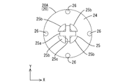
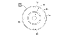
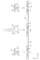
- the holding member 20 has a substantially circular shape as a whole when viewed in plan. As shown in FIGS. 7 and 9, the holding member 20 has a main body 24 along the bottom plate 14 a of the chassis 14 and the plate surface of the LED board 18, and protrudes from the main body 24 toward the back side, that is, the chassis 14 side. 14 and a fixing part 25 fixed to.
- the holding member 20 as a whole has a symmetrical shape with the central axis along the Z-axis direction as the center of symmetry.
- the main body portion 24 has a substantially circular shape when seen in a plan view, and is formed in a substantially straight plate shape along the X-axis direction and the Y-axis direction. As shown in FIG. 6, the main body portion 24 has a diameter that is substantially the same as the short side dimension (dimension in the Y-axis direction) of the LED substrate 18. And this main-body part 24 can be hold
- the main body 24 is arranged at a position where the center thereof coincides with the center position in the short side direction of the LED substrate 18. Therefore, the main body 24 can sandwich the LED board 18 with the chassis 14 over the entire length in the short side direction. At this time, both outer ends in the Y-axis direction of the main body portion 24 and both outer ends in the short side direction of the LED substrate 18 are substantially aligned. In other words, the main body 24 is almost entirely overlapped with the LED board 18 when viewed in plan, and is prevented from projecting outside the LED board 18.
- the diameter of the main body 24 is smaller than the interval (arrangement pitch) between the diffusion lenses 19 (LEDs 17) adjacent in the X-axis direction.
- the main body 24 is arranged in a region between the diffusion lenses 19 (LEDs 17) adjacent to each other in the X-axis direction in the LED substrate 18, that is, in a non-light emitting part in the LED substrate 18, There is no overlap when seen on a plane. That is, it is possible to avoid the main body 24 from obstructing light emission from the LED 17.
- the holding member 20 is arranged using the space and the holding member 20 is used. The LED substrate 18 is fixed.
- the fixing portion 25 can be locked to the bottom plate 14 a while penetrating through an attachment hole 14 e formed corresponding to the attachment position of the holding member 20 in the bottom plate 14 a of the chassis 14.
- the fixing portion 25 is disposed on the center side in the main body portion 24. Specifically, the fixing portion 25 is disposed at a position that is substantially concentric with the main body portion 24.
- the fixing portion 25 protrudes from the back side surface (the surface facing the chassis 14) of the main body portion 24 toward the back side, and a groove portion 25 c is provided at the tip portion thereof so as to be elastically engaged.
- the fixing portion 25 includes a base portion 25a that protrudes from the main body portion 24 to the back side, and an elastic locking piece 25b that protrudes further from the protruding tip of the base portion 25a toward the back side.
- the base portion 25a has a substantially cylindrical shape, the diameter of which is smaller than the mounting hole 14e of the chassis 14, and the insertion into the mounting hole 14e is allowed.
- the elastic locking piece 25 b is divided into four parts by making the groove part 25 c into a substantially cross shape when seen in a plan view.
- each elastic locking piece 25b is formed in a cantilever shape, and can be elastically deformed while constricting in the groove 25c with the protruding base end from the base 25a as a fulcrum. That is, the groove 25c is a bending space for each elastic locking piece 25b.
- On the outer surface of the elastic locking piece 25b there is provided a locking portion 25d that bulges outward, that is, on the side opposite to the groove 25c.
- the locking part 25d protrudes further outward than the outer peripheral surface of the base part 25a, and the diameter dimension (maximum diameter dimension) of the fixing part 25 at the bulging end is larger than the diameter dimension of the mounting hole 14e. It is said. In other words, the bulging end of the locking portion 25d is located outside the inner peripheral surface of the mounting hole 14e. Therefore, the locking portion 25d can be locked from the back side to the edge of the mounting hole 14e in the chassis 14, that is, the portion of the chassis 14 adjacent to the fixing portion 25. As described above, when the fixing portion 25 is inserted into the mounting hole 14e of the chassis 14, the elastic locking pieces 25b are elastically engaged with the edge portion from the back side after the elastic locking pieces 25b are passed through the mounting holes 14e.
- the holding member 20 can be fixed to the chassis 14 in an attached state.
- a plurality of mounting holes 14e are arranged in parallel in a matrix form along the X-axis direction and the Y-axis direction corresponding to the mounting position of each holding member 20 on the bottom plate 14a of the chassis 14.
- the main body 24 provided with the fixing portion 25 is arranged so that the entire area thereof overlaps with the LED substrate 18 in plan view. Accordingly, the fixing portion 25 is similarly arranged so as to overlap with the LED substrate 18 in a plan view. Therefore, the LED substrate 18 has a through hole 18b through which the fixing portion 25 is passed. As shown in FIG. 10, the through-hole 18b is arranged at a position on the LED board 18 between the adjacent LEDs 17 (diffuse lens 19), that is, a position where the LED 17 (diffuse lens 19) does not overlap with the LED 17 (diffuse lens 19). Has been.
- the through hole 18b has a horizontally long shape elongated in the X-axis direction when viewed in a plane, and both short side edges are formed in an arc shape.
- the through hole 18b has a short side dimension that just allows the insertion of the fixing portion 25, whereas the long side dimension has a larger margin.
- the through hole 18 b is configured to penetrate the LED substrate 18 along the Z-axis direction so that the fixing portion 25 can penetrate the LED substrate 18. It has become. Therefore, the LED substrate 18 can be positioned in the X-axis direction and the Y-axis direction by the fixing portion 25 that is passed through the through hole 18b.
- each of the reflection sheets 22 and 23 sandwiched between the main body portion 24 and the LED substrate 18 the position overlapping with the through hole 18 b in a plan view is shown in FIGS. 7, 9, and 11.
- communication holes 22c and 23c that can communicate with the through hole 18b and allow the fixing portion 25 to pass therethrough are formed.
- the main-body part 25 in the holding member 20 which concerns on this embodiment protrudes in the back side, ie, the reflective sheet 21 side (the LED board 18 side, the chassis 14 side), and the reflective sheet 21
- An abutting portion 26 that abuts against is provided.
- the contact portion 26 contacts the first reflection sheet 22 of the reflection sheet 21 and directly presses the first reflection sheet 22 from the front side, and the second reflection sheet 23 and the LED via the first reflection sheet 22. It is possible to indirectly hold the substrate 18 from the front side.
- this contact part 26 is a form which protrudes partially from the back side surface (opposite surface with the 1st reflective sheet 22) in the main-body part 24, the whole region of the back side surface of a main-body part is temporarily the 1st reflective sheet. Compared with the case where it contacts 22, the contact area with respect to the first reflection sheet 22 is small. In a state where the contact portion 26 is in contact with the first reflection sheet 22, the surface on the back side of the main body portion 24 floats from the first reflection sheet 22 and is kept in a non-contact state, and the back side of the main body portion 24. A gap C corresponding to the protruding dimension of the contact portion 26 is held between the surface of the first reflection sheet 22 and the surface of the first reflection sheet 22.
- the abutting portion 26 is disposed at a position away from the fixing portion 25 in the main body portion 24, specifically, an outer edge portion of the main body portion 24. That is, it can be said that the contact portion 26 is disposed at a position farthest from the fixed portion 25 disposed at the center of the main body portion 24.
- the main-body part 24 which concerns on this embodiment has the part elasticity from the fixing
- a total of four abutting portions 26 are provided in pairs at positions where the fixing portion 25 is sandwiched in the main body portion 24.
- each abutment portion 26 is disposed at a position at an angular interval of about 90 degrees in the main body portion 24, that is, on two straight lines that pass through the centers of the main body portion 24 and the fixing portion 25 and are orthogonal to each other. ing. That is, each contact portion 26 is disposed at a position that is symmetrical about the fixed portion 25 in the main body portion 24. Accordingly, the distances from the fixed portion 25 to each contact portion 26 are all the same. Further, it can be said that each contact portion 26 has a dot shape when the plate surface of the main body portion 24 is viewed in a plane.
- the contact points of the holding member 20 with respect to the first reflection sheet 22 are distributed and arranged at equal intervals in the plane of the plate surface of the main body portion 24, so that the holding member 20 is arranged with respect to the first reflection sheet 22. It can be supported stably without causing rattling (FIG. 6).
- each contact portion 26 has a substantially hemispherical shape as a whole, and its peripheral surface (contact surface with respect to the first reflection sheet 22) is formed of a spherical surface. Accordingly, each contact portion 26 is in point contact with the first reflection sheet 22. Thereby, the contact area of each contact part 26 with respect to the 1st reflective sheet 22 is made into the minimum.
- an inclined surface 24a is formed on the outer peripheral end surface of the main body 24 in the single-function holding member 20A.
- the inclined surface 24 a has a downward slope from the center side to the outer end side in the main body portion 24, thereby eliminating or reducing a step that may occur between the inclined surface 24 a and the first reflection sheet 22.
- the outer peripheral edge portion (the boundary portion with the reflection sheet 21) of the main body portion 24 is hardly visually recognized as luminance unevenness through the optical member 15.
- illustration is abbreviate
- the multifunctional holding member 20B has a support portion 27 that protrudes from the main body portion 24 toward the front side and can support the optical member 15 from the back side.
- the support portion 27 has a conical shape as a whole. Specifically, the support portion 27 is formed in a tapered shape so that the cross-sectional shape cut along the plate surface of the main body portion 24 is a circular shape, and the diameter dimension gradually decreases from the protruding proximal end side to the protruding distal end side. ing.
- the support portion 27 can be brought into contact with the diffusion plate 15a disposed on the backmost side (the LED 17 side) of the optical member 15, thereby supporting the diffusion plate 15a at a predetermined position. That is, the support portion 27 can regulate the positional relationship between the optical member 15 and the LED 17 in the Z-axis direction (direction perpendicular to the surface of the optical member 15) to a constant state.
- the outer diameter dimension of the protruding proximal end portion of the support portion 27 is smaller than both the short side dimension of the main body 24 and the short side dimension of the LED substrate 18. That is, it can be said that the support portion 27 has a point shape when viewed in a plane, whereas the main body portion 24 has a surface shape that covers a wider range when viewed in a plane than the support portion 27.
- the protruding dimension of the support portion 27 is substantially equal to the distance from the front surface of the main body portion 24 to the back surface of the diffuser plate 15a that is substantially straight along the X-axis direction and the Y-axis direction. . Therefore, the support portion 27 comes into contact with the diffusion plate 15a in a substantially straight state.
- the protruding tip portion that is a contact portion with the diffusion plate 15a is rounded. Since this support portion 27 is the only portion of the multifunctional holding member 20B that protrudes from the main body 24 to the front side, when performing the work of attaching the multifunctional holding member 20B to the chassis 14, the operator The support part 27 can be used as an operation part. Thereby, the attachment / detachment workability of the multifunctional holding member 20B can be improved.
- the support portion 27 is disposed at a substantially central position in the main body portion 24. That is, the support portion 27 is disposed at a position overlapping the fixing portion 25 disposed on the back side in a plan view. More specifically, the support portion 27 and the fixing portion 25 are arranged at positions that are substantially concentric when viewed in plan. With such an arrangement, when the operator uses the support portion 27 as the operation portion when performing the operation of attaching the multifunctional holding member 20B to the chassis 14, the support portion 27 exposed to the front side is visually observed. Thus, it is possible to easily grasp the position of the fixing portion 25 hidden behind the back side. Therefore, the workability at the time of inserting the fixing portion 25 into the communication holes 22c and 23c, the through hole 18b, and the mounting hole 14e can be improved.
- This embodiment has the structure as described above, and its operation will be described next.
- the liquid crystal panel 11 and the backlight device 12 are separately manufactured and assembled to each other using the bezel 13 or the like, whereby the liquid crystal display device 10 shown in FIGS. 4 and 5 is manufactured. Among these, the assembly work at the time of manufacturing the backlight device 12 will be described in detail.
- an operation of attaching the LED 17, the second reflection sheet 23, and the diffusion lens 19 to the LED substrate 18 is performed prior to assembling each component to the chassis 14. Specifically, first, as shown in FIG. 10, the LED 17 is mounted on a predetermined position on the LED substrate 18, and then the second reflection sheet 23 is put on the front side. At this time, each LED 17 of the second reflection sheet 23 is passed through each LED insertion hole 23a. Thereafter, as shown in FIG. 11, a diffusion lens 19 is attached to the LED substrate 18 so as to cover each LED 17. At this time, each attachment leg 19 d in the diffusing lens 19 is fixed to the LED substrate 18 by an adhesive through the leg insertion hole 23 b of the second reflection sheet 23. Thus, the light source unit U, in which the LED 17, the second reflection sheet 23, and the diffusing lens 19 are integrated with the LED substrate 18, is manufactured.
- each component to the chassis 14 The above-described light source unit U is housed inside from the front side of the chassis 14 through the opening 14b, and each light source unit U is arranged at a predetermined mounting position with respect to the bottom plate 14a. At this time, each through hole 18b of the LED board 18 in each light source unit U is aligned with each mounting hole 14e of the chassis 14 so as to communicate with each other.
- the LED boards 18 adjacent to each other in the X-axis direction can be connected to each other by fitting the adjacent connector portions 18a to each other.
- the connection work between the LED boards 18 arranged in the X-axis direction is not necessarily performed in the chassis 14 and may be performed outside the chassis 14.
- each lens insertion hole 22b in the first reflection sheet 22 is aligned with each diffusion lens 19 in the light source unit U, and each diffusion lens 19 is passed through each lens insertion hole 22b (FIG. 3).
- the first reflection sheet 22 is attached, the first reflection sheet 22 is overlapped from the front side with respect to almost all of the second reflection sheet 23 other than the portion overlapping the diffusing lens 19 in plan view (FIG. 7 and FIG. 8).
- the edge of the lens insertion hole 22 b in the first reflection sheet 22 is overlapped on the front side of the second reflection sheet 23 over the entire area. Further, as shown in FIG.
- the communication holes 22 c of the first reflection sheet 22 are aligned with the communication holes 23 c of the second reflection sheet 23, the through holes 18 b of the LED substrate 18, and the mounting holes 14 e of the chassis 14. Communicated. Thereafter, the holding member 20 is assembled.
- the support portion 27 can be used as the operation portion for the multifunctional holding member 20 ⁇ / b> B among the holding members 20.
- the operator can operate the multifunctional holding member 20B by holding the support portion 27.
- the multifunctional holding member 20B is accommodated inside through the opening 14b from the front side of the chassis 14, and the fixing part 25 hidden in the back side through the main body 24 is connected to the corresponding communication holes 22c and 23c, the through holes 18b, and Insert into the mounting hole 14e.
- the support portion 27 and the fixing portion 25 are arranged at positions that overlap each other and are concentric when viewed in a plane, the operator can easily grasp the position of the fixing portion 25.
- each elastic locking piece 25b is temporarily grooved while the fixing portion 25 is being inserted into the holes 14e, 18b, 22c, and 23c. It is elastically deformed so as to be confined in 25c. Thereafter, when the fixing portion 25 is inserted to a depth where each elastic locking piece 25b reaches the back side of the chassis 14, as shown in FIGS. 7 and 9, each elastic locking piece 25b is elastically restored and its locking is performed. The portion 25d is locked from the back side with respect to the edge of the mounting hole 14e. Thereby, the holding member 20 is prevented from being detached from the chassis 14 and is fixed in the attached state. In this state, the LED board 18 and the reflection sheets 22 and 23 are held together between the main body 24 and the bottom plate 14a of the chassis 14 in the holding member 20.
- each contact portion 26 provided in the main body portion 24 is connected to the front side of the first reflection sheet 22. It abuts on the surface. Therefore, in the mounted state, the spherical surface of each contact portion 26 is in point contact with the first reflection sheet 22, while the back surface of the main body portion 24 (with the first reflection sheet 22 and the first reflection sheet 22). Are opposed to the first reflection sheet 22 and kept in a non-contact state, and a contact portion is provided between the back surface of the main body 24 and the front surface of the first reflection sheet 22. A gap C corresponding to 26 projecting dimensions is retained.
- the contact area of the holding member 20 with respect to the first reflection sheet 22 is extremely small, and is smaller than the case where the entire area of the back side surface of the main body is brought into contact. In other words, the area of the portion of the first reflection sheet 22 that is not in contact with the holding member 20 (the portion that cannot be pressed by the holding member 20) is increased.
- the holding member 20 is stably supported by the four contact portions 26 arranged at symmetrical positions with an angular interval of about 90 degrees. More specifically, since each contact portion 26 is disposed on the outer edge portion of the main body portion 24, the contact portion 26 is disposed at a position overlapping the outer edge portion of the LED substrate 18 in the short side direction in a plan view.
- the outer edge part of the short side direction of the LED substrate 18 is pressed from the front side by each contact part 26.
- the first reflection sheet 22 is directly pressed by the contact portion 26, whereas the second reflection sheet 23 and the LED substrate 18 are indirectly pressed by the contact portion 26 through the first reflection sheet 22. ing.
- the fixing portion 25 penetrates the reflection sheets 22 and 23 and the LED board 18, the reflection sheets 22 and 23 and the LED board 18 are prevented from inadvertently moving in the X-axis direction and the Y-axis direction. The positioning in the same direction is achieved. Furthermore, since the fixing portion 25 has been fixed by passing through the mounting hole 14e formed in the chassis 14 and mechanically locked there, a fixing method using an adhesive or the like was temporarily adopted. Compared to the case, the fixing can be easily performed at a low cost, and the holding member 20 can be easily detached at the time of maintenance or disposal.
- the holding members 20 attached as described above are arranged at a plurality of locations different in the long side direction (X-axis direction) on each LED board 18. Thereby, each LED board 18 can be hold
- the optical member 15 is attached to the chassis 14 so as to cover the opening 14b.
- the specific mounting order of the optical member 15 is that the diffusion plate 15a is first and then the optical sheet 15b.
- the optical member 15 has an outer peripheral edge received by the receiving plate 14d of the chassis 14 and a central portion supported by the support 27 of each multifunctional holding member 20B. It is like that.
- the frame 16 is attached to the chassis 14, the outer peripheral edge of the optical member 15 is sandwiched between the frame 16 and the receiving plate 14d. Thereby, the manufacture of the backlight device 12 is completed.
- the liquid crystal panel 11 When assembling the manufactured backlight device 12 and the liquid crystal panel 11, the liquid crystal panel 11 is placed on the frame 16, and then the bezel 13 is put on the front side and screwed. As a result, the liquid crystal panel 11 is sandwiched between the frame 16 and the bezel 13 and the liquid crystal panel 11 is integrated with the backlight device 12, thereby completing the manufacture of the liquid crystal display device 10.
- each LED 17 provided in the backlight device 12 is turned on and an image signal is supplied to the liquid crystal panel 11, thereby A predetermined image is displayed on the display surface of the liquid crystal panel 11.
- the light emitted when each LED 17 is turned on first enters the light incident surface 19 a of the diffusion lens 19. At this time, most of the light is incident on the inclined surface of the light incident side recess 19c in the light incident surface 19a, so that the light enters the diffusing lens 19 while being refracted at a wide angle according to the inclination angle. The incident light propagates through the diffusing lens 19 and then exits from the light exit surface 19b.
- the light exit surface 19b has a flat, substantially spherical shape, an external air layer is formed. Light is emitted while being refracted at a wider angle at the interface.
- a light emitting side concave portion 19e having a substantially bowl shape is formed, and the peripheral surface has a flat and substantially spherical shape. Light can be emitted while being refracted at a wide angle on the peripheral surface of the light emitting side recess 19e, or reflected to the LED substrate 18 side. Of these, the light returned to the LED substrate 18 side is effectively utilized by being reflected by the second reflecting sheet 23 toward the diffusing lens 19 side and entering the diffusing lens 19 again, so that high luminance is obtained.
- the light having strong directivity emitted from the LED 17 can be diffused at a wide angle by the diffusing lens 19, so that the in-plane distribution of the optical member 15 in the light reaching the optical member 15 is uniform. It can be.
- the region between the adjacent LEDs 17 becomes difficult to be visually recognized as a dark part by using the diffusing lens 19, it becomes possible to widen the interval between the LEDs 17, and thus the number of the LEDs 17 arranged while suppressing the luminance unevenness. Reduction can be achieved.
- the interval between the adjacent LEDs 17 can be widened, so that the holding member 20 can be arranged using the widened area, and the holding member 20 is further reduced.
- the LED substrate 18 can be fixed.
- each LED 17 generates heat with lighting. Most of the heat generated from each LED 17 is propagated to the chassis 14 via the mounted LED substrate 18 and then dissipated to the air outside the liquid crystal display device 10. Considering the heat dissipation efficiency at this time, the higher the degree of close contact between the LED board 18 and the chassis 14, the better the heat transfer between them, so that the heat release efficiency increases, and conversely, the closeness degree between the LED board 18 and the chassis 14. The lower the is, the lower the heat transfer properties of both, and the lower the heat dissipation efficiency.
- the LED substrate 18 is fixed to the chassis 14 by the holding member 20 and the following configuration is adopted to improve the heat dissipation efficiency.
- the LED substrate 18 is stably held in close contact with the chassis 14 because the outer edge portion in the short side direction is pressed from the front side by the contact portions 26 in the holding member 20.
- the holding member 20 has the fixing portion 25 on the center side of the main body portion 24 and each contact portion 26 on the outer edge portion, the LED substrate 18 is pressed by the center fixing portion 25 from the back side.
- the LED board 18 can be pressed down more stably with sufficient balance.
- the LED board 18 is stably fixed in close contact with the chassis 14 by the holding member 20, the heat transfer to the chassis 14 is extremely high, thereby enabling efficient heat dissipation. It is. Therefore, since the inside of the backlight device 12 is unlikely to become high temperature, it is possible to suppress a decrease in the light emission efficiency of each LED 17, and thus it is possible to stably obtain high luminance.
- each LED 17 in the backlight device 12 is turned on or off, so that a change occurs in the internal temperature environment, and accordingly each configuration of the liquid crystal display device 10.
- Parts can expand or contract thermally.
- the first reflective sheet 22 and the second reflective sheet 23 are thermally expanded or contracted, if local deformation such as wrinkles or bending occurs temporarily, unevenness occurs in the reflected light. As a result, brightness unevenness occurs in the light emitted from the backlight device 12, and the display quality may be adversely affected.
- the LED substrate 18 is thermally expanded or contracted, if a local deformation such as warping or bending occurs, contact failure occurs in the connector portion 18a, and lighting control of the LED 17 is performed.
- Such local deformation that may occur in each of the reflection sheets 22 and 23 and the LED board 18 is likely to occur in proportion to the magnitude of the pressing force acting from the chassis 14 and the holding member 20 and the area (contact area) acting. In order to suppress local deformation, it is preferable to reduce the pressing force or to reduce the area of the pressed portion.
- the holding member 20 is provided with a contact portion 26, and the contact portion 26 of the holding member 20 is brought into point contact with the first reflection sheet 22.
- the contact area with respect to the first reflection sheet 22 is reduced.
- the portion pressed by the holding member 20 (the portion overlapping the contact of the contact portion 26 in a plan view) is reduced and held.
- the area of the portion that is not pressed by the member 20 (the portion that does not overlap with the contact point of the contact portion 26 in a plan view) increases.
- the portion pressed by the holding member 20 is relatively restricted in expansion and contraction due to thermal expansion or contraction (the degree of freedom of expansion and contraction is low), whereas the portion not pressed by the holding member 20 is relatively Expansion and contraction associated with thermal expansion or contraction is easily tolerated (high degree of freedom of expansion and contraction).
- the degree of freedom of expansion and contraction is low
- the portion not pressed by the holding member 20 is relatively Expansion and contraction associated with thermal expansion or contraction is easily tolerated (high degree of freedom of expansion and contraction).
- the area of the unpressed portion is increased, each of the reflection sheets 22 and 23 and the LED board 18 are easily expanded and contracted due to thermal expansion or thermal contraction as a whole. Therefore, the flatness as a whole is maintained, and thus the reflection sheets 22 and 23 and the LED substrate 18 are locally bent and warped. It is suppressed to become.
- the contact portion 26 is disposed at a position away from the fixed portion 25 in the main body portion 24.
- the abutment portion 26 is a portion that applies a pressing force from the front side (the main body portion 24 side) to each of the reflection sheets 22 and 23 and the LED substrate 18, whereas the fixing portion 25 is provided with each of the reflection sheets 22 and 23.
- 23 and the LED board 18 are portions that apply pressing force from the back side (chassis 14 side). Therefore, as described above, the contact portion 26 and the fixing portion 25 are arranged so as to be shifted (offset) from each other in plan view, so that the pressing force is applied from the front side in each of the reflection sheets 22 and 23 and the LED substrate 18.
- the position where the position (the position of the contact portion 26) acts and the position where the pressing force acts from the back side (the position of the locking portion 25d) are similarly shifted. Therefore, it is possible to avoid the stress acting from the front side and the back side from being concentrated on each of the reflection sheets 22 and 23 and the LED substrate 18. Thereby, since it can prevent that the pressing force which acts on each reflective sheet 22,23 and LED board 18 becomes large locally, the freedom degree of the expansion-contraction in the part pressed by the holding member 20 becomes extremely low. Therefore, the degree of freedom of expansion and contraction of the reflecting sheets 22 and 23 and the LED board 18 as a whole can be increased.
- the following actions and effects can be obtained by disposing the contact portion 26 at a position away from the fixed portion 25 in the main body portion 24. That is, when a dimensional error occurs in manufacturing the holding member 20, for example, the protruding dimension of the contact part 26 from the main body part 24 becomes larger than a set value, or the length dimension of the fixed part 25 is set value. If it becomes shorter than that, the pressing force acting on each of the reflection sheets 22 and 23 and the LED substrate 18 may become excessively large (more than necessary). Therefore, in the present embodiment, a certain degree of elasticity is imparted to the portion of the main body portion 24 from the fixed portion 25 to the abutting portion 26 according to the above configuration, so that as shown in FIG.
- the pressing force that can be increased can be absorbed by elastically deforming the portion from the fixing portion 25 to the contact portion 26. Thereby, it is possible to prevent an excessive pressing force from acting on the reflecting sheets 22 and 23 and the LED substrate 18 from the contact portion 26. Accordingly, the degree of freedom of expansion and contraction in each of the reflection sheets 22 and 23 and the LED substrate 18 can be ensured.
- the backlight device 12 of the present embodiment includes the LED 17 that is a light source, the chassis 14 that houses the LED 17, the reflective sheet 21 that is an extending member that extends along the inner surface of the chassis 14, and the LED substrate. 18 and a holding member 20 fixed to the chassis 14 with the reflection sheet 21 and the LED board 18 sandwiched between the chassis 14 and the holding member 20 projecting toward the reflection sheet 21 and the LED board 18. A contact portion 26 that is in contact with the reflective sheet 21 and the LED substrate 18 is provided.
- the holding member 20 is fixed to the chassis 14, the reflection sheet 21 and the LED substrate 18 are held in a state of being sandwiched between the holding member 20 and the chassis 14.
- the holding member 20 is provided with a contact portion 26 that protrudes toward the reflection sheet 21 and the LED substrate 18, and the contact portion 26 contacts the reflection sheet 21 and the LED substrate 18.
- the contact area of the holding member 20 with respect to the reflection sheet 21 can be reduced. In other words, the reflective sheet 21 and the LED substrate 18 are not in contact with the holding member 20 and the area of the portion that cannot be pressed by the holding member 20 increases.
- This unpressed portion is more easily expanded and contracted when thermal expansion or contraction occurs due to a change in the thermal environment, compared to the portion pressed by the holding member 20 in contact. And if the area of this unpressed part becomes large, since the freedom degree of expansion / contraction will increase as the reflection sheet 21 and the LED board 18 as a whole, deformation such as bending and warping accompanying expansion / contraction becomes locally evident. Can be suppressed.
- the contact portion (the contact portion 26) of the holding member 20 is contacted.
- the holding member 20 includes a main body 24 that sandwiches the reflection sheet 21 and the LED substrate 18 with the chassis 14, and a fixing portion 25 that protrudes from the main body 24 toward the chassis 14 and is fixed to the chassis 14.
- the contact portion 26 is provided in the main body portion 24. In this way, when the fixing portion 25 is fixed to the chassis 14, the reflection sheet 21 and the LED substrate 18 sandwiched between the main body portion 24 and the chassis 14 are suitably held. At this time, the abutting portion 26 abuts on the reflection sheet 21, and the entire surface of the main body portion 24 facing the reflection sheet 21 is avoided.
- the contact portion 26 is disposed at a position away from the fixed portion 25 in the main body portion 24.
- a pressing force acts on the reflection sheet 21 and the LED board 18 from both the chassis 14 side and the main body 24 side.
- the position where the pressing force acts from the chassis 14 side and the position where the pressing force acts from the main body portion 24 side depend on the positional relationship between the contact portion 26 and the fixing portion 25. is doing.
- the contact portion 26 is disposed at a position away from the fixed portion 25 in the main body portion 24, the position where the pressing force acts on the reflection sheet 21 and the LED substrate 18 from the chassis 14 side, and the main body The position where the pressing force acts from the side of the portion 24 is shifted (offset) from each other as viewed in a plane. Therefore, for example, the stress acting on the reflective sheet 21 and the LED board 18 is dispersed as compared with the case where the positions where the respective pressing forces act on the reflective sheet 21 and the LED board 18 are the same as viewed in plan. And stress concentration can be reduced. Thereby, the freedom degree of the expansion / contraction in the reflective sheet 21 and the LED board 18 can be raised.
- the holding member 20 when a dimensional error occurs in manufacturing the holding member 20, for example, when the projecting dimension of the contact part 26 from the main body part 24 becomes larger than a set value, it acts on the reflection sheet 21 and the LED substrate 18. There is a risk that the holding force to be excessively increased. Even in such a case, since the contact part 26 is arranged at a position away from the fixed part 25 in the main body part 24, the part of the main body part 24 from the fixed part 25 to the contact part 26 is elastically deformed. It becomes possible to absorb the pressing force that can be increased. Thereby, it is possible to prevent an excessive pressing force from acting on the reflection sheet 21 and the LED substrate 18 from the contact portion 26, and thus it is possible to ensure the degree of freedom of expansion and contraction in the reflection sheet 21 and the LED substrate 18.
- the fixing portion 25 is disposed on the center side of the main body portion 24
- the contact portion 26 is disposed on the outer edge portion of the main body portion 24.
- the holding member 20 can be stably fixed to the chassis 14 by arranging the fixing portion 25 on the center side of the main body portion 24.
- the contact part 26 is arranged on the outer edge part of the main body part 24, the distance between the fixed part 25 and the contact part 26 can be secured to the maximum, so that the stress concentration can be alleviated better. Therefore, the degree of freedom of expansion and contraction in the reflection sheet 21 and the LED substrate 18 can be further increased.
- the main body portion 24 can be more easily elastically deformed, which occurs when the holding member 20 is manufactured.
- the absorption width of the dimensional error can be increased, so that the degree of freedom of expansion and contraction in the reflective sheet 21 and the LED substrate 18 can be more stably ensured.
- the fixing portion 25 is arranged on the center side in the main body portion 24, at least a pair of the abutting portions 26 are arranged at positions where the fixing portion 25 is sandwiched in the main body portion 24.
- the holding member 20 can be stably fixed to the chassis 14 by arranging the fixing portion 25 on the center side of the main body portion 24.
- the pair of contact portions 26 are arranged at positions sandwiching the fixed portion 25, the pressing force can be applied to the reflective sheet 21 and the LED substrate 18 in a balanced manner.
- the contact part 26 is arranged at a symmetrical position with the fixed part 25 as the center. In this way, the pressing force can be applied to the reflective sheet 21 and the LED substrate 18 in a more balanced manner.
- the fixing portion 25 is fixed to the chassis 14 while penetrating the reflection sheet 21 and the LED substrate 18. If it does in this way, it will become possible to position reflective sheet 21 and LED board 18 about the direction which meets the plate surface by fixed part 25 which penetrates reflective sheet 21 and LED board 18.
- the fixing portion 25 penetrates the reflection sheet 21, the LED board 18, and the chassis 14, and is locked to the chassis 14 from the side opposite to the reflection sheet 21 and the LED board 18 side.
- the holding member 20, the reflection sheet 21, and the LED substrate 18 can be fixed by locking the fixing portion 25 penetrating the chassis 14 together with the reflection sheet 21 and the LED substrate 18 to the chassis 14. Therefore, it is not necessary to use other fixing means such as an adhesive, and fixing can be easily performed at low cost.
- An optical member 15 is disposed at a position facing the LED 17, and a support portion 27 that protrudes toward the optical member 15 side and supports the optical member 15 is provided on the main body portion 24 of the composite holding member 20 ⁇ / b> B. ing. In this way, the multifunctional holding member 20B that fixes the reflective sheet 21 and the LED substrate 18 can have a function of supporting the optical member 15 together.
- the fixed portion 25 and the support portion 27 are arranged at positions where they are overlapped with each other when viewed in a plane. In this way, when the operator attaches the multi-function holding member 20B while holding the support portion 27, the position of the fixing portion 25 can be easily grasped, so that the workability is excellent.
- the fixed portion 25 and the support portion 27 are arranged at positions that are concentric with each other. In this way, workability is further improved.
- the abutting portion 26 has a point-like shape as viewed in a plane. In this way, the contact portion 26 is brought into point contact with the reflective sheet 21, so that the contact area can be made as small as possible, thereby increasing the degree of freedom of expansion and contraction in the reflective sheet 21 and the LED substrate 18. it can.
- the abutting surface with respect to the reflection sheet 21 and the LED substrate 18 is configured by a curved surface. If it does in this way, the reflective sheet 21 becomes easy to slip with respect to the contact part 26, and the freedom degree of expansion / contraction can be raised further.
- the contact portion 26 is configured by a spherical contact surface. If it does in this way, the reflective sheet 21 and the LED board 18 will slip more easily with respect to the contact part 26, and the freedom degree of expansion / contraction can be raised further.
- the extending member is an LED substrate 18 having LEDs 17.
- the degree of freedom of expansion and contraction associated with thermal expansion or contraction in the LED board 18 is increased, so that contact failure is unlikely to occur at the connection location with an external circuit or the like, and lighting control of the LED 17 is performed. It is possible to prevent problems from occurring when performing.
- a plurality of LEDs 17 are arranged in parallel on the LED substrate 18. In this way, a plurality of LEDs 17 can be efficiently arranged on the LED substrate 18, which is suitable for increasing the brightness.
- the holding member 20 is disposed between the adjacent LEDs 17. In this way, the space held between the adjacent LEDs 17 can be used effectively. Further, it is possible to prevent the holding member 20 from obstructing the light emitted from the LED 17.
- the extending member is a reflection sheet 21 that reflects light from the LED 17. If it does in this way, light can be utilized effectively by reflecting light with the reflective sheet 21, and it becomes suitable for the improvement of a brightness
- the extending member includes an LED substrate 18 having LEDs 17 and a reflection sheet 21 that reflects light from the LEDs 17, and the LED substrate 18 and the reflection sheet 21 together with the holding member 20 in a state of being overlapped with each other. It is sandwiched between the chassis 14. In this way, the LED board 18 and the reflection sheet 21 can be collectively held by the holding member 20. In addition, the degree of freedom of expansion and contraction accompanying thermal expansion or contraction in the LED substrate 18 and the reflection sheet 21 is increased.
- the reflection sheet 21 is disposed on the opposite side of the LED board 18 from the chassis 14 side, and the lens insertion hole 22b and the LED insertion hole 23a through which the LED 17 passes in a position overlapping the LED 17 when seen in a plan view. have.
- the light can be used more effectively by reflecting the light by the reflection sheet 21 disposed on the opposite side of the chassis 14 side with respect to the LED substrate 18, for example to improve luminance. Preferred.
- the reflection sheet 21 has the lens insertion hole 22b and the LED insertion hole 23a, it is avoided that the light emission from LED17 is prevented.
- a diffusing lens 19 for diffusing the light from the LED 17 is disposed at a position overlapping the LED 17 when seen in a plan view. In this way, the light emitted from the LED 17 can be emitted after being diffused by the diffusion lens 19. Thereby, unevenness is less likely to occur in the emitted light.
- the reflection sheet 21 is interposed between the first reflection sheet 22 having a size that allows the lens insertion hole 22b to pass the diffusion lens 19, the LED substrate 18 and the diffusion lens 19, and viewed in plan.
- a second reflection that is disposed at a position overlapping the lens insertion hole 22b provided in the first reflection sheet 22 (located in the lens insertion hole 22b in a plan view) and reflects light toward the diffusion lens 19 side.
- a sheet 23 In this way, even if the first reflection sheet 22 is provided with a lens insertion hole 22b having a size for allowing the diffusion lens 19 to pass therethrough, the lens insertion hole 22b is disposed at a position overlapping the lens insertion hole 22b (viewing the lens in a plan view). Light can be reflected toward the diffuser lens 19 by the second reflecting sheet 23 (which is disposed in the hole 22b). As a result, light can be used effectively, which is suitable for improving luminance.
- edge of the lens insertion hole 22b in the first reflection sheet 22 and the second reflection sheet 23 are formed so as to overlap each other when seen in a plan view. If it does in this way, the edge part of lens penetration hole 22b in the 1st reflective sheet 22 and the 2nd reflective sheet 23 will be connected seamlessly in the plane. Thereby, light can be utilized more effectively.
- Embodiment 1 of this invention was shown, this invention is not restricted to the said embodiment, For example, the following modifications can also be included.
- members similar to those in the above embodiment are denoted by the same reference numerals as those in the above embodiment, and illustration and description thereof may be omitted.
- the contact portion 26-1 is formed in an annular shape so as to surround the center-side fixing portion 25 in the main body portion 24.
- the abutting portion 26-1 has an annular shape and extends along the outer edge portion of the main body portion 24.
- the contact portion 26-1 has a linear shape that draws a circle when seen in a plane, and is an endless ring.
- the abutting portion 26-1 has a semicircular cross section, and the abutting surface with respect to the first reflecting sheet 22 is a spherical surface.
- the annular contact portion 26-1 surrounds the gap C held between the main body portion 24 and the first reflection sheet 22, so that the gap C is formed in the chassis 14. Opening is avoided. Therefore, the light in the chassis 14 is prevented from leaking into the gap C, whereby the chassis 14 is opened from the gap slightly held between the fixing portion 25 and the mounting hole 14e of the chassis 14 via the gap C. It is possible to prevent light from leaking outside.
- the fixing portion 25 is disposed on the center side of the main body portion 24, whereas the contact portion 26-1 is formed in an annular shape so as to surround the fixing portion 25. .
- the holding member 20 can be stably fixed to the chassis 14 by arranging the fixing portion 25 on the center side of the main body portion 24.
- the annular contact portion 26-1 surrounding the fixing portion 25 is in contact with the first reflection sheet 22, each reflection sheet 22, 23 and the LED substrate 18 are held in a balanced manner and more appropriately. Can do.
- the gap C held between the main body 24 and the first reflection sheet 22 is surrounded by the annular contact portion 26-1, it is possible to prevent the gap C from opening into the chassis 14. .
- the light in the chassis 14 can be prevented from leaking into the gap C. Furthermore, for example, when a gap is formed between the fixed portion 25 and the chassis 14 (mounting hole 14e), light in the chassis 14 is prevented from leaking out of the chassis 14 through the gap C. can do.
- the contact portion 26-1 is formed in a linear shape when viewed in a plane. In this way, the contact portion 26-1 is in line contact with the first reflection sheet 22, so that each of the reflection sheets 22 and 23 and the LED substrate 18 are reduced while reducing the contact area with the first reflection sheet 22. Can be held appropriately.
- a restricting portion 28 that protrudes toward the front side and can come into contact with the main body portion 24 from the back side.
- the restricting portion 28 is disposed over the entire edge of the mounting hole 14e-2 and has a short cylindrical shape as a whole.
- the outer diameter dimension of the restricting portion 28 is larger than that of the fixed portion 25, and the reflection sheets 22 and 23 and the holes 18 b, 22 c and 23 c of the LED substrate 18 allow the insertion of the restricting portion 28.
- Have a size of The protruding dimension of the restricting portion 28 from the bottom plate 14a-2 is larger than the sum of the thickness dimensions of the reflecting sheets 22 and 23 and the LED board 18.
- the holding member 20 when the holding member 20 is attached to the chassis 14-2, the main body portion 24 and the contact portion 26 are supported at a position away from the first reflection sheet 22 by the restriction portion 28. That is, the holding member 20 is restricted in the Z-axis direction positional relationship with the first reflection sheet 22 by the restriction portion 28 and is kept in a non-contact state with the first reflection sheet 22. In this way, the holding force does not directly act on the reflecting sheets 22 and 23 and the LED board 18 from the holding member 20, so that the thermal expansion in the reflecting sheets 22 and 23 and the LED board 18 or The degree of freedom of expansion and contraction during heat contraction can be made extremely high.
- the holding member 20 cannot have a constant finish at the time of manufacture, and some dimensional errors can occur. Depending on the finish, even if the positional relationship of the holding member 20 with respect to the first reflection sheet 22 is restricted by the restriction portion 28, the holding member 20 may come into contact with the first reflection sheet 22. Even in such a situation, in the present embodiment, since the main body portion 24 has the abutting portion 26, only the abutting portion 26 with respect to the first reflective sheet 22 as shown in FIG. Are in contact with each other, and the entire region of the main body 24 is avoided from contacting. Thereby, the freedom degree of expansion / contraction at the time of thermal expansion or thermal contraction in each reflective sheet 22, 23 and LED board 18 can be kept high.
- the restricting portion 28 that restricts the positional relationship of the holding member 20 with respect to the first reflecting sheet 22 so that a gap is held between the holding member 20 and the first reflecting sheet 22.
- the holding member 20 is restricted in the positional relationship with respect to the first reflection sheet 22 by the restricting portion 28, a gap is held between the holding member 20 and the first reflection sheet 22.
- 23 and the LED board 18 are easily expanded and contracted as they thermally expand or contract.
- the abutting portion 26 abuts against the first reflective sheet 22. Therefore, the degree of freedom of expansion and contraction in each of the reflection sheets 22 and 23 and the LED substrate 18 is compared with the case where the surface of the holding member facing the first reflection sheet 22 is in contact with the first reflection sheet 22 over the entire area. Can be kept high.
- the regulating portion 28-3 is provided integrally with the holding member 20.
- the restricting portion 28-3 is provided at a position adjacent to the fixed portion 25 in the main body portion 24 of the holding member 20.
- the restricting portion 28-3 is configured to be continuous with the base portion 25a of the main body portion 24 and the fixing portion 25.
- the restricting portion 28-3 is configured to surround the base portion 25a.
- Embodiment 2 A second embodiment of the present invention will be described with reference to FIG. 24 or FIG. In this Embodiment 2, what changed the structure of the contact part 126 is shown. In addition, the overlapping description about the same structure, effect
- the abutting portion 126 is disposed at a position adjacent to the fixed portion 25 in the main body portion 24.
- the contact portion 126 is configured to surround the base portion 25a of the fixed portion 25 over the entire circumference and is connected to the base portion 25a. That is, the base portion 25a of the fixing portion 25 has a form in which the diameter of the connecting base end portion with respect to the main body portion 24 is partially expanded by the contact portion 126. Thereby, reinforcement of the fixing
- the surface of the contact portion 126 facing the back side is in surface contact with the first reflective sheet 22.
- the contact portion 126 has a square shape when seen in a plan view, but the specific shape can be changed as appropriate, such as a circular shape or an elliptical shape.
- the position pressed from the front side by the abutting portion 126 and the position pressed from the back side by the locking portion 25 d are substantially the same position as viewed from above.
- the contact portion 126 is connected to the fixed portion 25.
- the strength of the contact part 126 and the fixed part 25 can be increased as compared with the case where the contact part is independent of the fixed part 25.
- the contact portion 126 is configured to surround the fixed portion 25. The strength of the contact part 126 and the fixed part 25 can be further improved.
- Embodiment 2 of this invention was shown, this invention is not restricted to the said embodiment, For example, the following modifications can also be included.
- members similar to those in the above embodiment are denoted by the same reference numerals as those in the above embodiment, and illustration and description thereof may be omitted.
- the communication hole 22c-1 in the first reflection sheet 22-1 is enlarged in diameter to allow insertion of the contact portion 126-1. That is, the communication hole of the first reflection sheet 22-1 is larger in diameter than the communication hole 23c of the second reflection sheet 23 and the through hole 18b of the LED board 18.
- the projecting dimension of the contact part 126-1 from the main body part 24 is larger than that described in the second embodiment by the thickness of the first reflection sheet 22-1. Therefore, when the holding member 20 is attached to the chassis 14, the abutting portion 126-1 is abutted against the edge portion of the communication hole 23c in the second reflecting sheet 23.
- the pressing force from the contact part 26 acts only on the 2nd reflective sheet 23 and the LED board 18, and does not act on the 1st reflective sheet 22-1. Therefore, the degree of freedom of expansion and contraction at the time of thermal expansion or contraction is further enhanced for the first reflection sheet 22-1.
- the communication hole 23c-2 in the second reflection sheet 23-2 is enlarged in diameter to allow insertion of the contact portion 126-2. That is, the communication hole 23c-2 of the second reflection sheet 23-2 is equal in diameter to the communication hole 22c-1 of the first reflection sheet 22-1 and larger than the through hole 18b of the LED substrate 18.
- the projecting dimension of the contact part 126-2 from the main body part 24 is larger than that described in the first modification by the thickness of the second reflection sheet 23-2. Therefore, when the holding member 20 is attached to the chassis 14, the abutting portion 126-2 is abutted against the edge portion of the through hole 18b in the LED substrate 18.
- the pressing force from the contact portion 126-2 acts only on the LED substrate 18 and does not act on the first reflection sheet 22-1 and the second reflection sheet 23-2. Therefore, the first reflective sheet 22-1 and the second reflective sheet 23-2 have a higher degree of freedom of expansion and contraction during thermal expansion or thermal contraction.
- Embodiment 3 of the present invention will be described with reference to FIGS.
- the structure of the holding member 220 is changed.
- action, and effect as above-mentioned Embodiment 1 is abbreviate
- the holding member 220 has a two-part configuration, and a first part 29 having a main body part 224 and a fixing part 225 and a first part 29 that is detachably assembled to the first part 29 from the front side. It consists of two parts 30.
- the first component 29 is provided with a mounting opening 29a that allows the second component 30 to be mounted so as to open to the front side.
- the mounting opening 29 a penetrates through the main body 224 in the first component 29 and is formed to a depth over the entire length of the base 225 a in the fixing part 225. Therefore, the mounting opening 29 a communicates with a groove 225 c formed in the fixed portion 225.
- the mounting opening 29a is also opened to the back side through the groove 225c.
- the mounting opening 29a has a circular cross section.
- An inclined surface 29b facing the mounting opening 29a is provided on the inner surface of each elastic locking piece 225b forming the fixing portion 225.
- the inclined surface 29b is disposed on the protruding base end portion of the elastic locking piece 225b.
- the inclined surface 29b has a gradient gradually projecting inward from the protruding proximal end side of the elastic locking piece 225b toward the protruding distal end side, whereby the protruding proximal end portion of the elastic locking piece 225b
- the shape is thinner at the end side and thicker at the protruding tip side.
- the fixed portion 225 has a substantially constant diameter over its entire length, and is a little smaller than each of the reflection sheets 22 and 23, the LED board 18 and the holes 14e, 18b, 22c, and 23c of the chassis 14.
- Each elastic locking piece 225b is not provided with the locking portion 25d as shown in the first embodiment.
- the second part 30 has a substantially T-shaped cross section, and includes a base part 30a parallel to the main body part 224 of the first part 29 and a shaft part 30b protruding from the base part 30a toward the back side.
- the base portion 30 a has a substantially circular shape when seen in a plan view, and is approximately the same size as the main body portion 224 of the first component 29.
- the shaft portion 30b has a substantially cylindrical shape whose diameter is substantially constant over the entire length, and the protruding size from the base portion 30a is approximately the same as the size of the first component 29 in the Z-axis direction.
- the shaft portion 30b has a slightly smaller diameter than the mounting opening 29a of the first component 29, and can be inserted into and removed from the mounting opening 29a.
- the first component 29 is attached to the chassis 14 in advance.
- the fixing portion 225 in the first component 29 is inserted into each of the reflection sheets 22 and 23, the LED board 18, and each of the holes 14 e, 18 b, 22 c, and 23 c of the chassis 14.
- the fixing portion 225 is not locked with respect to the chassis 14.
- the second component 30 is mounted on the first component 29 from the front side.
- the shaft portion 30b of the second component 30 is inserted from the front side into the mounting opening 29a of the first component 29, and when the predetermined depth is reached, the tip portion of the shaft portion 30b becomes an inclined surface 29b of each elastic locking piece 225b. Abutted.
- the inclined surface 29b is pressed by the tip of the shaft portion 30b, so that each elastic locking piece is guided by the inclination.
- 225b is elastically deformed to open outward. That is, each elastic locking piece 225b is elastically deformed by being spread by the shaft portion 30b and is locked to the edge of the mounting hole 14e.
- Each elastic locking piece 225b is restricted from elastically returning inward (deformed to close) by having the shaft portion 30b disposed on the inner side thereof. Thereby, it is possible to prevent a situation in which the holding member 220 is inadvertently detached from the chassis 14. Note that when the elastic locking pieces 225b are pushed out by the shaft portion 30b, the elastic locking pieces 225b may be plastically deformed.
- the holding member 220 protrudes toward the chassis 14 from the main body 224 that sandwiches the reflection sheets 22 and 23 and the LED board 18 between the holding member 220 and the chassis 14.
- a fixing portion 225 fixed to the chassis 14, and the fixing portion 225 is elastically deformable and is locked to the opposite side of the reflective sheets 22 and 23 and the LED substrate 18 while penetrating the chassis 14.
- the holding member 220 includes a first part 29 having a main body part 224 and a fixing part 225, and an elastic deformation of the elastic locking piece 225b attached to the first part 29. And the second part 30 that regulates.
- the second reflection sheet 23 shown in the first embodiment is omitted, and instead the light is reflected on the front side surface of the LED substrate 318 as shown in FIG.
- the reflective layer 318d is formed.
- the reflective layer 318d exhibits a white color with excellent light reflectivity, and is formed, for example, by printing a paste containing a metal oxide on the surface of the LED substrate 318.
- As the printing means screen printing, ink jet printing and the like are suitable.
- the formation range of the reflective layer 318d can be almost the entire surface of the front surface of the LED substrate 318, but can also be only the portion of the LED substrate 318 that faces the diffusing lens 19.
- the light returned from the diffusion lens 19 side by the reflection layer 318d can be reflected again toward the diffusion lens 19.
- only the 1st reflection sheet 22 will be pinched
- FIG. 32 only the 1st reflection sheet 22 will be pinched
- the first reflection sheet 422 is provided with an LED insertion hole 422e having a size (which is smaller than the lens insertion hole 22b shown in the first embodiment) that allows the LEDs 17 to pass therethrough. It can be placed directly.
- the region between the LEDs 17 tends to be visually recognized as a dark part, and therefore the arrangement pitch of the LEDs 17 in the X-axis direction and the Y-axis direction is narrower than that in the first embodiment. It is preferable to prevent luminance unevenness.
- the present invention is not limited to the embodiments described with reference to the above description and drawings.
- the following embodiments are also included in the technical scope of the present invention.
- the specific shape of the contact portion can be changed as appropriate.
- the present invention includes those in which the abutting portion has a columnar shape, a prismatic shape, a conical shape, a pyramid shape, or the like, and those in which the cross-sectional shape in the abutting portion is a mountain shape (triangle) or an elliptical shape.
- the contact portion when the contact portion is a columnar or prismatic shape, the contact portion is in surface contact with the extending member (each reflection sheet or LED substrate), and the contact portion is conical. Or when it is made into a pyramid shape, the top part of a contact part will be in point contact with respect to an extending member.
- the abutting portion has a linear shape with a predetermined length when viewed in a plane, or an elliptical endless annular shape, a rectangular endless annular shape, an endless annular shape (such as a C-shape) when viewed in a plane. And the like are also included in the present invention.
- the contact portion disposed at a position away from the fixed portion is disposed on the outer edge portion of the main body portion. It is also possible to arrange the contact portion at a position other than the outer edge portion of the main body portion, specifically at a position between the outer edge portion and the fixing portion in the main body portion. In that case, it is also possible to arrange
- the four main body portions having the point-like contact portions as viewed in a plan view are provided.
- the number of the contact portions provided in the main body portion is three or less or Of course, it is possible to use five or more.
- the portion of the main body between the fixed portion and the contact portion is made elastic.
- the present invention includes a configuration in which the main body portion is set to be hardly or not elastically deformed at all. Even in such a case, the positions where the pressing force acts on the extending member (each reflecting sheet or LED substrate) from the front side and the back side are shifted from each other as viewed in a plane, so that the stress on the extending member Concentration can be suitably relaxed, and the effect of increasing the degree of freedom of expansion and contraction can be obtained.
- the fixing portion is disposed at a position that is concentric with the main body portion.
- the fixing portion is disposed at a position that is shifted from the center of the main body portion.
- the abutting portion is preferably arranged on a straight line connecting the fixed portion and the center of the main body portion. It is possible to secure the maximum distance.
- the contact portion that is connected to the fixed portion is configured to surround the fixed portion.
- the contact portion that is connected to the fixed portion is the fixed portion. What is made into the form which is not enclosed, ie, the contact part is continued in a part of base, is also contained in this invention.
- the shape of the main body portion of the holding member can be appropriately changed.
- the present invention includes a configuration in which the main body portion has an elliptical shape or a rectangular shape (rectangular shape or square shape) when viewed in a plan view.
- the holding member is exemplified to be configured between adjacent LEDs in the LED substrate.
- the holding member overlaps with the LED when viewed in plan on the LED substrate. What was arranged is also included in the present invention.
- the holding member is preferably provided with an insertion hole in a portion overlapping with the LED.
- the attachment position and the number of attachments of the holding member to each LED substrate can be appropriately changed.
- the attachment position and the number of attachments of the holding member to the chassis can be changed as appropriate.
- the fixing portion of the holding member is locked in a state of penetrating the mounting hole with respect to the chassis.
- a specific fixing method of the fixing portion with respect to the chassis is appropriately Can be changed.
- the present invention includes a configuration in which the mounting hole and the elastic locking piece are omitted, and the base portion penetrating the through hole of the LED board is fixed to the inner wall surface of the chassis with an adhesive or the like. In that case, means such as welding and welding can be employed in addition to the adhesive.
- the multi-function holding member is shown in which the support portion is disposed at a position that is concentric with the main body portion. What is arranged is also included in the present invention.
- the present invention includes an arrangement in which the support portion and the fixing portion are arranged so as not to overlap each other when seen in a plan view.
- the multi-function holding member is shown in which the support portion has a tapered conical shape.
- the support portion having a tapered pyramid shape is also included in the present invention. It is. Further, the support portion does not necessarily have to be tapered, and the support portion having a cylindrical shape or a prism shape having a constant diameter is also included in the present invention.
- the support portion of the multifunctional holding member has a point shape in the plane of the optical member.
- the support portion has a linear shape in the plane of the optical member.
- those formed in a planar shape in the plane of the optical member are also included in the present invention.
- the surface of the holding member is exemplified as white.
- the color of the surface of the holding member may be milky white or silver, for example. Further, the color of the surface can be set by applying a desired color paint to the surface of the holding member.
- the “extending member” includes the reflective sheet.
- the present invention includes a configuration in which the reflective sheet is omitted.
- the “extending member” includes the LED substrate.
- the present invention includes a configuration in which the LED substrate is omitted.
- a discharge tube such as a cold cathode tube may be used as the light source, or a planar light source such as an organic EL may be used.
- the reflective sheet and the LED substrate are exemplified as the “extending member”.
- the heat radiating member may be an “extending member”.
- the LED board is used in an appropriate combination of the five-mounting type, the six-mounting type, and the eight-mounting type, but other than five, six, and eight. What used the LED board which mounted the number of LED is also contained in this invention.
- an LED chip that emits blue light in a single color and a LED that emits white light using a phosphor is used.
- an LED chip that emits ultraviolet light in a single color is used.
- a built-in LED that emits white light with a phosphor is also included in the present invention.
- the present invention includes an LED using a type of LED in which three types of LED chips each emitting C (cyan), M (magenta), and Y (yellow) are monochromatic.
- an LED using white light emitting LED is shown.
- an LED emitting red light, an LED emitting blue light, and an LED emitting green light are used in appropriate combination. May be.
- the one using the diffusion lens that diffuses the light from the LED is shown, but the one using an optical lens other than the diffusion lens (for example, a condensing lens) is also the present invention. include.
- the screen size and the aspect ratio of the liquid crystal display device can be changed as appropriate.
- the liquid crystal panel and the chassis are illustrated in a vertically placed state in which the short side direction coincides with the vertical direction.
- the liquid crystal panel and the chassis have the long side direction in the vertical direction.
- Those that are in a vertically placed state matched with are also included in the present invention.
- a TFT is used as a switching element of a liquid crystal display device.
- the present invention can also be applied to a liquid crystal display device using a switching element other than TFT (for example, a thin film diode (TFD)).
- a switching element other than TFT for example, a thin film diode (TFD)
- the present invention can also be applied to a liquid crystal display device for monochrome display.
- the liquid crystal display device using the liquid crystal panel as the display panel has been exemplified.
- the present invention is applicable to display devices using other types of display panels.
- the television receiver provided with the tuner is illustrated, but the present invention is also applicable to a display device that does not include the tuner.
- each holding member has been described as a “single function type” and a “multifunction type” in order to distinguish between the two types of holding members. Thus, it does not mean that it has no function other than the function of holding the extending member.
- the names “single-function type” and “multi-function type” are given for convenience of explanation based on the presence or absence of a support function for the optical member, and a “single-function type” holding member is attached to the holding function. It does not preclude having a function (for example, a positioning function for the extending member) or other additional functions.
- SYMBOLS 10 Liquid crystal display device (display device), 11 ... Liquid crystal panel (display panel), 12 ... Backlight device (illumination device), 14 ... Chassis, 14e ... Mounting hole, 15 ... Optical member, 17 ... LED (light source), 18, 318 ... LED substrate (light source substrate, extending member), 19 ... diffusion lens, 20, 20A, 20B, 220 ... holding member, 21 ... reflecting sheet (reflecting member, extending member), 22, 422 ... first Reflection sheet (first reflection member, extension member), 22b ... lens insertion hole (light source insertion hole), 23 ... second reflection sheet (second reflection member, extension member), 23a ...
- LED insertion hole (light source) Insertion hole) 24, 224 ... main body, 25, 225 ... fixed part, 25b, 225b ... elastic locking piece, 26, 226 ... contact part, 27 ... support part, 28 ... regulating part, 29 ... first part 30 ... second part, 422e ... L D insertion hole (light source insertion hole), C ... gap, TV ... television receiver apparatus
Abstract
Priority Applications (2)
| Application Number | Priority Date | Filing Date | Title |
|---|---|---|---|
| US13/375,549 US8648979B2 (en) | 2009-06-15 | 2010-04-06 | Lighting device, display device and television receiver |
| CN2010800262485A CN102459993A (zh) | 2009-06-15 | 2010-04-06 | 照明装置、显示装置以及电视接收装置 |
Applications Claiming Priority (2)
| Application Number | Priority Date | Filing Date | Title |
|---|---|---|---|
| JP2009142445 | 2009-06-15 | ||
| JP2009-142445 | 2009-06-15 |
Publications (1)
| Publication Number | Publication Date |
|---|---|
| WO2010146913A1 true WO2010146913A1 (fr) | 2010-12-23 |
Family
ID=43356242
Family Applications (1)
| Application Number | Title | Priority Date | Filing Date |
|---|---|---|---|
| PCT/JP2010/056204 WO2010146913A1 (fr) | 2009-06-15 | 2010-04-06 | Dispositif d'éclairage, dispositif d'affichage et récepteur de télévision |
Country Status (3)
| Country | Link |
|---|---|
| US (1) | US8648979B2 (fr) |
| CN (1) | CN102459993A (fr) |
| WO (1) | WO2010146913A1 (fr) |
Cited By (5)
| Publication number | Priority date | Publication date | Assignee | Title |
|---|---|---|---|---|
| US9222654B2 (en) | 2013-03-14 | 2015-12-29 | Lsi Industries, Inc. | Luminaires and luminaire mounting structures |
| US9441796B2 (en) | 2013-03-14 | 2016-09-13 | Lsi Industries, Inc. | Luminaire with long chains of lower power LEDs and multiple on-board LED drivers |
| JP2016181354A (ja) * | 2015-03-23 | 2016-10-13 | シャープ株式会社 | 反射シート、バックライト装置、表示装置及びテレビジョン受信機 |
| JP2018018643A (ja) * | 2016-07-27 | 2018-02-01 | 三菱電機株式会社 | 面光源装置および液晶表示装置 |
| US10788708B2 (en) | 2016-07-27 | 2020-09-29 | Mitsubishi Electric Corporation | Planar light source device and liquid crystal display device |
Families Citing this family (11)
| Publication number | Priority date | Publication date | Assignee | Title |
|---|---|---|---|---|
| EP2426396B1 (fr) * | 2009-06-15 | 2015-11-25 | Sharp Kabushiki Kaisha | Dispositif d'éclairage, dispositif d'affichage et récepteur de télévision |
| WO2010146916A1 (fr) * | 2009-06-15 | 2010-12-23 | シャープ株式会社 | Dispositif d'éclairage, dispositif d'affichage et récepteur de télévision |
| US20120147592A1 (en) * | 2009-09-04 | 2012-06-14 | Sharp Kabushiki Kaisha | Electronic package, lighting device, and display device |
| CN103090272B (zh) * | 2013-01-25 | 2015-08-12 | 京东方科技集团股份有限公司 | 一种直下式背光模组及显示装置 |
| CN103712131B (zh) | 2013-12-27 | 2016-03-30 | 京东方科技集团股份有限公司 | 一种背光模组、显示装置 |
| KR102294163B1 (ko) * | 2014-12-05 | 2021-08-27 | 쑤저우 레킨 세미컨덕터 컴퍼니 리미티드 | 발광 모듈 |
| KR102291662B1 (ko) * | 2015-02-02 | 2021-08-20 | 삼성디스플레이 주식회사 | 표시 장치 |
| US9759416B2 (en) * | 2015-07-14 | 2017-09-12 | Lsi Industries, Inc. | Luminaires and thermal management apparatuses |
| CN109814293B (zh) * | 2017-11-20 | 2022-03-01 | 群创光电股份有限公司 | 背光模块与显示装置 |
| CN108153046B (zh) * | 2017-12-08 | 2021-02-02 | 深圳创维-Rgb电子有限公司 | 一种直下式液晶模组及其电视机 |
| US11002433B2 (en) | 2018-07-31 | 2021-05-11 | Nichia Corporation | Light fixture and method for mounting light fixture |
Citations (5)
| Publication number | Priority date | Publication date | Assignee | Title |
|---|---|---|---|---|
| JP2002184510A (ja) * | 2000-12-13 | 2002-06-28 | Sumitomo Wiring Syst Ltd | コネクタ |
| JP2006276761A (ja) * | 2005-03-30 | 2006-10-12 | Sharp Corp | 液晶表示装置 |
| JP2007322697A (ja) * | 2006-05-31 | 2007-12-13 | Sony Corp | バックライト装置及び液晶表示装置 |
| JP2008198398A (ja) * | 2007-02-08 | 2008-08-28 | Sony Corp | バックライト装置及び表示装置 |
| JP2009129707A (ja) * | 2007-11-22 | 2009-06-11 | Sony Corp | バックライト装置及び液晶表示装置 |
Family Cites Families (6)
| Publication number | Priority date | Publication date | Assignee | Title |
|---|---|---|---|---|
| TWI317829B (en) * | 2004-12-15 | 2009-12-01 | Epistar Corp | Led illumination device and application thereof |
| JP2007317423A (ja) | 2006-05-24 | 2007-12-06 | Harison Toshiba Lighting Corp | バックライトユニット |
| CN101165566A (zh) * | 2006-10-20 | 2008-04-23 | 鸿富锦精密工业(深圳)有限公司 | 直下式背光模组 |
| TWI330741B (en) * | 2006-11-02 | 2010-09-21 | Au Optronics Corp | Supporting structure and backlight module using the same |
| KR101394024B1 (ko) * | 2007-06-26 | 2014-05-12 | 엘지이노텍 주식회사 | 광원 장치 |
| KR101405595B1 (ko) * | 2007-12-18 | 2014-06-12 | 엘지이노텍 주식회사 | 발광 모듈 접속 장치 및 이를 구비한 라이트 유닛 |
-
2010
- 2010-04-06 US US13/375,549 patent/US8648979B2/en active Active
- 2010-04-06 CN CN2010800262485A patent/CN102459993A/zh active Pending
- 2010-04-06 WO PCT/JP2010/056204 patent/WO2010146913A1/fr active Application Filing
Patent Citations (5)
| Publication number | Priority date | Publication date | Assignee | Title |
|---|---|---|---|---|
| JP2002184510A (ja) * | 2000-12-13 | 2002-06-28 | Sumitomo Wiring Syst Ltd | コネクタ |
| JP2006276761A (ja) * | 2005-03-30 | 2006-10-12 | Sharp Corp | 液晶表示装置 |
| JP2007322697A (ja) * | 2006-05-31 | 2007-12-13 | Sony Corp | バックライト装置及び液晶表示装置 |
| JP2008198398A (ja) * | 2007-02-08 | 2008-08-28 | Sony Corp | バックライト装置及び表示装置 |
| JP2009129707A (ja) * | 2007-11-22 | 2009-06-11 | Sony Corp | バックライト装置及び液晶表示装置 |
Cited By (5)
| Publication number | Priority date | Publication date | Assignee | Title |
|---|---|---|---|---|
| US9222654B2 (en) | 2013-03-14 | 2015-12-29 | Lsi Industries, Inc. | Luminaires and luminaire mounting structures |
| US9441796B2 (en) | 2013-03-14 | 2016-09-13 | Lsi Industries, Inc. | Luminaire with long chains of lower power LEDs and multiple on-board LED drivers |
| JP2016181354A (ja) * | 2015-03-23 | 2016-10-13 | シャープ株式会社 | 反射シート、バックライト装置、表示装置及びテレビジョン受信機 |
| JP2018018643A (ja) * | 2016-07-27 | 2018-02-01 | 三菱電機株式会社 | 面光源装置および液晶表示装置 |
| US10788708B2 (en) | 2016-07-27 | 2020-09-29 | Mitsubishi Electric Corporation | Planar light source device and liquid crystal display device |
Also Published As
| Publication number | Publication date |
|---|---|
| US8648979B2 (en) | 2014-02-11 |
| CN102459993A (zh) | 2012-05-16 |
| US20120075550A1 (en) | 2012-03-29 |
Similar Documents
| Publication | Publication Date | Title |
|---|---|---|
| WO2010146913A1 (fr) | Dispositif d'éclairage, dispositif d'affichage et récepteur de télévision | |
| JP5184701B2 (ja) | 照明装置、表示装置、及びテレビ受信装置 | |
| JP5133457B2 (ja) | 照明装置、表示装置、及びテレビ受信装置 | |
| JP5244241B2 (ja) | 光源ユニット、照明装置、表示装置、及びテレビ受信装置 | |
| JP5244240B2 (ja) | 照明装置、表示装置、及びテレビ受信装置 | |
| WO2010146916A1 (fr) | Dispositif d'éclairage, dispositif d'affichage et récepteur de télévision | |
| JP5259825B2 (ja) | 照明装置、表示装置、及びテレビ受信装置 | |
| JP5303657B2 (ja) | 照明装置、表示装置、及びテレビ受信装置 | |
| JP4951152B2 (ja) | 照明装置、表示装置、及びテレビ受信装置 | |
| JP5337883B2 (ja) | 照明装置、表示装置、及びテレビ受信装置 | |
| JP5079889B2 (ja) | 照明装置、表示装置及びテレビ受信装置 | |
| WO2011093119A1 (fr) | Dispositif d'éclairage, dispositif d'affichage et récepteur de télévision | |
| WO2010146917A1 (fr) | Dispositif d'éclairage, dispositif d'affichage et récepteur de télévision | |
| WO2011111444A1 (fr) | Dispositif d'éclairage, appareil d'affichage et récepteur de télévision | |
| WO2013080882A1 (fr) | Dispositif d'éclairage, dispositif d'affichage, et dispositif de récepteur de télévision | |
| WO2011013455A1 (fr) | Dispositif d'éclairage, dispositif d'affichage et dispositif de réception de télévision | |
| KR20110075857A (ko) | 액정표시장치 |
Legal Events
| Date | Code | Title | Description |
|---|---|---|---|
| WWE | Wipo information: entry into national phase |
Ref document number: 201080026248.5 Country of ref document: CN |
|
| 121 | Ep: the epo has been informed by wipo that ep was designated in this application |
Ref document number: 10789290 Country of ref document: EP Kind code of ref document: A1 |
|
| WWE | Wipo information: entry into national phase |
Ref document number: 13375549 Country of ref document: US |
|
| NENP | Non-entry into the national phase |
Ref country code: DE |
|
| 122 | Ep: pct application non-entry in european phase |
Ref document number: 10789290 Country of ref document: EP Kind code of ref document: A1 |
|
| NENP | Non-entry into the national phase |
Ref country code: JP |