WO2010143489A1 - 表示用駆動回路およびそれを備える基板モジュール - Google Patents
表示用駆動回路およびそれを備える基板モジュール Download PDFInfo
- Publication number
- WO2010143489A1 WO2010143489A1 PCT/JP2010/057998 JP2010057998W WO2010143489A1 WO 2010143489 A1 WO2010143489 A1 WO 2010143489A1 JP 2010057998 W JP2010057998 W JP 2010057998W WO 2010143489 A1 WO2010143489 A1 WO 2010143489A1
- Authority
- WO
- WIPO (PCT)
- Prior art keywords
- parallel
- input terminal
- display
- signal
- terminal group
- Prior art date
Links
Images


Classifications
-
- G—PHYSICS
- G09—EDUCATION; CRYPTOGRAPHY; DISPLAY; ADVERTISING; SEALS
- G09G—ARRANGEMENTS OR CIRCUITS FOR CONTROL OF INDICATING DEVICES USING STATIC MEANS TO PRESENT VARIABLE INFORMATION
- G09G3/00—Control arrangements or circuits, of interest only in connection with visual indicators other than cathode-ray tubes
- G09G3/20—Control arrangements or circuits, of interest only in connection with visual indicators other than cathode-ray tubes for presentation of an assembly of a number of characters, e.g. a page, by composing the assembly by combination of individual elements arranged in a matrix no fixed position being assigned to or needed to be assigned to the individual characters or partial characters
- G09G3/34—Control arrangements or circuits, of interest only in connection with visual indicators other than cathode-ray tubes for presentation of an assembly of a number of characters, e.g. a page, by composing the assembly by combination of individual elements arranged in a matrix no fixed position being assigned to or needed to be assigned to the individual characters or partial characters by control of light from an independent source
- G09G3/36—Control arrangements or circuits, of interest only in connection with visual indicators other than cathode-ray tubes for presentation of an assembly of a number of characters, e.g. a page, by composing the assembly by combination of individual elements arranged in a matrix no fixed position being assigned to or needed to be assigned to the individual characters or partial characters by control of light from an independent source using liquid crystals
- G09G3/3611—Control of matrices with row and column drivers
- G09G3/3685—Details of drivers for data electrodes
-
- G—PHYSICS
- G09—EDUCATION; CRYPTOGRAPHY; DISPLAY; ADVERTISING; SEALS
- G09G—ARRANGEMENTS OR CIRCUITS FOR CONTROL OF INDICATING DEVICES USING STATIC MEANS TO PRESENT VARIABLE INFORMATION
- G09G3/00—Control arrangements or circuits, of interest only in connection with visual indicators other than cathode-ray tubes
- G09G3/20—Control arrangements or circuits, of interest only in connection with visual indicators other than cathode-ray tubes for presentation of an assembly of a number of characters, e.g. a page, by composing the assembly by combination of individual elements arranged in a matrix no fixed position being assigned to or needed to be assigned to the individual characters or partial characters
- G09G3/2092—Details of a display terminals using a flat panel, the details relating to the control arrangement of the display terminal and to the interfaces thereto
- G09G3/2096—Details of the interface to the display terminal specific for a flat panel
-
- G—PHYSICS
- G02—OPTICS
- G02F—OPTICAL DEVICES OR ARRANGEMENTS FOR THE CONTROL OF LIGHT BY MODIFICATION OF THE OPTICAL PROPERTIES OF THE MEDIA OF THE ELEMENTS INVOLVED THEREIN; NON-LINEAR OPTICS; FREQUENCY-CHANGING OF LIGHT; OPTICAL LOGIC ELEMENTS; OPTICAL ANALOGUE/DIGITAL CONVERTERS
- G02F1/00—Devices or arrangements for the control of the intensity, colour, phase, polarisation or direction of light arriving from an independent light source, e.g. switching, gating or modulating; Non-linear optics
- G02F1/01—Devices or arrangements for the control of the intensity, colour, phase, polarisation or direction of light arriving from an independent light source, e.g. switching, gating or modulating; Non-linear optics for the control of the intensity, phase, polarisation or colour
- G02F1/13—Devices or arrangements for the control of the intensity, colour, phase, polarisation or direction of light arriving from an independent light source, e.g. switching, gating or modulating; Non-linear optics for the control of the intensity, phase, polarisation or colour based on liquid crystals, e.g. single liquid crystal display cells
- G02F1/133—Constructional arrangements; Operation of liquid crystal cells; Circuit arrangements
- G02F1/1333—Constructional arrangements; Manufacturing methods
- G02F1/1345—Conductors connecting electrodes to cell terminals
- G02F1/13452—Conductors connecting driver circuitry and terminals of panels
-
- G—PHYSICS
- G02—OPTICS
- G02F—OPTICAL DEVICES OR ARRANGEMENTS FOR THE CONTROL OF LIGHT BY MODIFICATION OF THE OPTICAL PROPERTIES OF THE MEDIA OF THE ELEMENTS INVOLVED THEREIN; NON-LINEAR OPTICS; FREQUENCY-CHANGING OF LIGHT; OPTICAL LOGIC ELEMENTS; OPTICAL ANALOGUE/DIGITAL CONVERTERS
- G02F1/00—Devices or arrangements for the control of the intensity, colour, phase, polarisation or direction of light arriving from an independent light source, e.g. switching, gating or modulating; Non-linear optics
- G02F1/01—Devices or arrangements for the control of the intensity, colour, phase, polarisation or direction of light arriving from an independent light source, e.g. switching, gating or modulating; Non-linear optics for the control of the intensity, phase, polarisation or colour
- G02F1/13—Devices or arrangements for the control of the intensity, colour, phase, polarisation or direction of light arriving from an independent light source, e.g. switching, gating or modulating; Non-linear optics for the control of the intensity, phase, polarisation or colour based on liquid crystals, e.g. single liquid crystal display cells
- G02F1/133—Constructional arrangements; Operation of liquid crystal cells; Circuit arrangements
- G02F1/1333—Constructional arrangements; Manufacturing methods
- G02F1/1345—Conductors connecting electrodes to cell terminals
- G02F1/13454—Drivers integrated on the active matrix substrate
-
- G—PHYSICS
- G09—EDUCATION; CRYPTOGRAPHY; DISPLAY; ADVERTISING; SEALS
- G09G—ARRANGEMENTS OR CIRCUITS FOR CONTROL OF INDICATING DEVICES USING STATIC MEANS TO PRESENT VARIABLE INFORMATION
- G09G2300/00—Aspects of the constitution of display devices
- G09G2300/04—Structural and physical details of display devices
- G09G2300/0421—Structural details of the set of electrodes
- G09G2300/0426—Layout of electrodes and connections
-
- G—PHYSICS
- G09—EDUCATION; CRYPTOGRAPHY; DISPLAY; ADVERTISING; SEALS
- G09G—ARRANGEMENTS OR CIRCUITS FOR CONTROL OF INDICATING DEVICES USING STATIC MEANS TO PRESENT VARIABLE INFORMATION
- G09G2330/00—Aspects of power supply; Aspects of display protection and defect management
- G09G2330/06—Handling electromagnetic interferences [EMI], covering emitted as well as received electromagnetic radiation
-
- G—PHYSICS
- G09—EDUCATION; CRYPTOGRAPHY; DISPLAY; ADVERTISING; SEALS
- G09G—ARRANGEMENTS OR CIRCUITS FOR CONTROL OF INDICATING DEVICES USING STATIC MEANS TO PRESENT VARIABLE INFORMATION
- G09G2370/00—Aspects of data communication
- G09G2370/08—Details of image data interface between the display device controller and the data line driver circuit
-
- H—ELECTRICITY
- H05—ELECTRIC TECHNIQUES NOT OTHERWISE PROVIDED FOR
- H05K—PRINTED CIRCUITS; CASINGS OR CONSTRUCTIONAL DETAILS OF ELECTRIC APPARATUS; MANUFACTURE OF ASSEMBLAGES OF ELECTRICAL COMPONENTS
- H05K1/00—Printed circuits
- H05K1/02—Details
- H05K1/14—Structural association of two or more printed circuits
- H05K1/148—Arrangements of two or more hingeably connected rigid printed circuit boards, i.e. connected by flexible means
-
- H—ELECTRICITY
- H05—ELECTRIC TECHNIQUES NOT OTHERWISE PROVIDED FOR
- H05K—PRINTED CIRCUITS; CASINGS OR CONSTRUCTIONAL DETAILS OF ELECTRIC APPARATUS; MANUFACTURE OF ASSEMBLAGES OF ELECTRICAL COMPONENTS
- H05K2201/00—Indexing scheme relating to printed circuits covered by H05K1/00
- H05K2201/10—Details of components or other objects attached to or integrated in a printed circuit board
- H05K2201/10007—Types of components
- H05K2201/10128—Display
- H05K2201/10136—Liquid Crystal display [LCD]
Definitions
- the present invention relates to a display driving circuit and a substrate module including the same, and more particularly to a display driving circuit having two or more types of input interface terminals and a substrate module including the same.
- a display driving circuit for driving a display unit such as a liquid crystal display device has been mounted, for example, in the form of a chip on a glass substrate, and a flexible printed wiring (Flexible Printed Circuit) connected to the glass substrate.
- FPC Flexible printed wiring
- the transmission system for video signals given from the outside via this FPC board is roughly divided into two types of interface specifications: a serial system and a parallel system. Usually, either one of these methods is adopted, but these methods may be used together.
- one device such as a mobile phone or a portable computer includes two or more display units and a corresponding number of display drive circuits.
- a video signal is transmitted in a parallel manner to a drive circuit of a display unit close to a main board that generates a video signal, and a video signal is transmitted in a serial manner to a drive circuit of a display part far from the main board. Is transmitted.
- a different display drive circuit corresponding to only one of the interface specifications for each drive circuit of each display unit.
- the manufacturing cost of the device increases. To rise.
- a display drive circuit provided with input terminals corresponding to the above two types of interface specifications is used, a drive circuit having the same configuration (same type) can be used for any display unit. Manufacturing costs can be reduced.
- any display device can be used.
- the drive circuit having the same configuration can be used in common, the manufacturing cost can also be reduced.
- Japanese Utility Model Publication No. 1-79137 discloses a configuration of a graphic display device corresponding to both parallel interface and serial interface specifications.
- the display drive circuit provided with the input terminals corresponding to the two types of interface specifications has a larger number of input terminals than the case where only one type is supported, the display drive circuit in which the input terminals are arranged.
- the outer peripheral size, particularly the length of the long side thereof is increased.
- the display driving circuit is disposed in the vicinity of the display unit, and generally provided with a display output terminal along the long side close to the display unit, and on the opposite side (that is, the side close to the FPC board).
- An input terminal is provided along the long side. Therefore, the total length of the output terminals multiplied by the distance between the terminals (pitch) (of the entire output terminal) is greater than the length of the total number of input terminals multiplied by the distance between the terminals (pitch) (of the entire input terminal). In the case of being small, the length of the long side of the display drive circuit becomes larger as the number of input terminals increases.
- the circuit size (especially, the length of the long side) is increased, it may be difficult to provide the circuit on a glass substrate having a limited arrangement area. Further, when a chip including the circuit is manufactured from one wafer, the larger the chip size, the smaller the number that can be manufactured from one wafer, resulting in an increase in manufacturing cost of the display drive circuit.
- the present invention provides a display drive in which the length of the long side is smaller (than the length when all the input terminals are arranged in a line) when input terminals corresponding to two or more types of interface specifications are provided.
- An object of the present invention is to provide a circuit and a substrate module including the circuit.
- a first aspect of the present invention is a display driving circuit that has a rectangular shape having a long side and a short side, and is to be provided on a transparent substrate including a display unit that displays an image.
- a first input terminal group for receiving a first signal based on a first interface specification;
- a second input terminal group for receiving a second signal based on a second interface specification using a signal having a smaller amplitude value or higher frequency than the first interface specification;
- An output terminal group for providing the display unit with a display signal for displaying the image, which is generated based on at least one of the first and second signals,
- the output terminal group and at least a part of the first input terminal group are arranged along one of the long sides,
- the second input terminal group is arranged along the other of the long sides.
- the first signal includes a parallel data signal and a parallel clock signal based on a parallel interface specification
- the second signal includes a serial data signal and a serial clock signal based on a serial interface specification.
- the first input terminal group arranged along one of the long sides includes a parallel input terminal for receiving at least a part of the parallel data signal and the parallel clock signal.
- the parallel input terminal is disposed in the vicinity of the short side.
- parallel input terminals for receiving at least part of the parallel data signal and the parallel clock signal are arranged along the short side.
- the second input terminal group arranged along the other of the long sides includes an input terminal for receiving the serial data signal and the serial signal.
- a display driving circuit and a display unit according to the first aspect of the present invention, A transparent substrate; Display wiring formed on the transparent substrate, for transmitting the display signal from the output terminal group to the display unit, An input wiring line formed on the transparent substrate for transmitting at least one of the first and second signals given from the outside to at least one of the first and second input terminal groups; Prepared, The display driving circuit is arranged such that one of the long sides on which the output terminal group is arranged is close to the display unit.
- the first signal includes a parallel data signal and a parallel clock signal based on a parallel interface specification
- the second signal includes a serial data signal and a serial clock signal based on a serial interface specification
- the first input terminal group arranged along one of the long sides includes a parallel input terminal for receiving at least a part of the parallel data signal and the parallel clock signal.
- a ninth aspect of the present invention is the eighth aspect of the present invention,
- the display driving circuit is attached as a circuit chip on the transparent substrate,
- the parallel input terminal is disposed in the vicinity of the short side,
- the input wiring connected to the parallel input terminal is arranged to pass through the short side from the lower side of the circuit chip.
- a tenth aspect of the present invention is the eighth aspect of the present invention,
- the input wiring connected to the parallel input terminal is wider than the input wiring connected to the second input terminal group arranged along the other of the long sides.
- the output terminal group and at least a part of the first input terminal group are arranged along one of the long sides of the display drive circuit, and the second input terminal group is Since it is arranged along the other of the long sides, the length of the long side can be made smaller (than the length when all the input terminals are arranged in a line), and the manufacturing cost can be reduced.
- the second aspect of the present invention it is possible to reduce the length of the long side by appropriately arranging the first and second input terminal groups that receive signals based on the parallel interface specification and the serial interface specification.
- the manufacturing cost can be reduced.
- a parallel input terminal that receives at least a part of a parallel data signal and a parallel clock signal that can be transmitted even when the wiring impedance is large because the amplitude is typically relatively large and the frequency is low.
- the length of the long side can be reduced, and the manufacturing cost can be reduced.
- the power supply line and the ground line in the parallel interface specification usually require a small wiring impedance, it is preferable that they are not included in the parallel input terminal and are not arranged along one of the long sides.
- the parallel input terminal is arranged in the vicinity of the short side
- the output terminal group arranged along the same long side as the parallel input terminal does not interfere with the output terminal group. Since the wiring can be provided directly under the short side or in the vicinity of the short side, the wiring distance from the parallel input terminal can be reduced, and the wiring impedance can be reduced.
- the parallel input terminal is arranged along the short side, the length of the long side can be reduced, and the manufacturing cost can be reduced.
- the wiring distance from the parallel input terminal can be reduced and the wiring impedance can be reduced as compared with the case where the output terminal group is arranged along the long side.
- the input terminal for receiving the serial data signal and the serial signal is arranged along the long side on the side different from the output terminal group, for example, for input from an FPC board or the like
- the wiring can be shortened, and the wiring impedance can be reduced.
- a (display) substrate module such as a liquid crystal module
- a display drive circuit that exhibits the same effect as the first aspect of the present invention.
- a (display) substrate module such as a liquid crystal module
- a display drive circuit that exhibits the same effect as the third aspect of the present invention.
- the input wiring connected to the parallel input terminal disposed in the vicinity of the short side is disposed so as to pass through the short side from the lower side of the circuit chip.
- the wiring impedance can be reduced.
- the input wiring connected to the parallel input terminals is wider than the input wiring connected to the second input terminal group, so that the wiring distance increases. Regardless, the wiring impedance can be reduced.
- FIG. 1st liquid crystal module in the said embodiment it is a schematic plan view which shows the structure of the 1st liquid crystal module in the said embodiment.
- FIG. 2nd liquid crystal module in the said embodiment It is the top view which looked at the LSI chip in the said embodiment, and its peripheral part from the back surface side of the glass substrate.
- FIG. 1st liquid crystal module in the said embodiment it is a schematic plan view which shows the structure of the 1st liquid crystal module in the said embodiment.
- 2nd liquid crystal module in the said embodiment It is the top view which looked at the LSI chip in the said embodiment, and its peripheral part from the back surface side of the glass substrate.
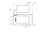
- FIG. 1 is a perspective view schematically showing a configuration of a liquid crystal display device according to an embodiment of the present invention
- FIG. 2 is a schematic plan view showing the configuration.
- the liquid crystal display device is a portable information terminal such as a PDA (Personal Digital Assistant) or a mobile phone terminal, and includes a first liquid crystal module 110 and a main substrate 100, and a first housing for storing them. 1 housing 101, a second liquid crystal module 210, and a second housing 201 for housing the same. Further, the first liquid crystal module 110 and the main board 100 are connected by a first FPC board 150, and the second liquid crystal module 210 and the main board 100 are connected by a second FPC board 250. Yes.
- the arrangement positions, sizes, shapes, and the like of the respective components are described so as to be different from actual ones for easy viewing.
- the portable information terminal which is a liquid crystal display device has two screens displayed by the first and second liquid crystal modules 110 and 210.
- any display device having approximately two or more screens can be applied without changing the above-described configuration in the present embodiment.
- the present invention can be similarly applied to a single-screen display device, but details will be described later in a modification.
- the second FPC board 250 is connected to a serial interface connector 152 provided on the main board 100, and the first FPC board 150 is placed on the main board 100. It is connected to a parallel interface connector 151 provided.
- the number of signal lines required for the serial interface is less than the number of signal lines required for the parallel interface (including power supply etc.), and signal transmission through the serial interface is possible. If this is done, there is an effect in reducing electromagnetic interference (EMI), and therefore, the second FPC board 250 having a long transmission distance may perform signal transmission through a serial interface. However, if signal transmission is performed using a serial interface, power consumption increases, and therefore, the first FPC board 150 having a long transmission distance may perform signal transmission using a parallel interface.
- EMI electromagnetic interference
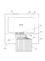
- FIG. 3 is a schematic plan view showing the configuration of the first liquid crystal module 110 according to the embodiment of the present invention.
- FIG. 4 shows the configuration of the second liquid crystal module 210 according to the embodiment of the present invention. It is a schematic plan view. Note that the arrangement positions and shapes of the components shown in these drawings are different from the actual ones for the sake of easy viewing.
- the first liquid crystal module 110 is provided with two glass substrates 120 and 125 arranged to face each other and an LSI chip 140 for driving display. Further, an electronic component such as a capacitor may be provided. Similarly, in the second liquid crystal module 210, as shown in FIG. 4, two glass substrates 220 and 225 arranged opposite to each other and a display having the same configuration as that provided in the first liquid crystal module 110 are used. And an LSI chip 140 for driving.
- a display unit 130 in which liquid crystal (not shown) is sealed with a sealing material (not shown) is formed.
- An LSI chip 140 having a driver function necessary for driving a liquid crystal and a first FPC board 150 connected to the outside are mounted on the overhanging portion 120a of the glass substrate 120.
- the LSI chip 140 displays a video by giving a display signal to the display unit 130. .
- a display portion 230 in which liquid crystal is sealed is formed in a space between the glass substrates 220 and 225.
- An LSI chip 140 and a second FPC board 250 are mounted. When a video signal transmitted from the main board to the LSI chip 140 via the second FPC board 250 by the serial interface is given, the LSI chip 140 gives a display signal to the display unit 230 to display the video.
- the LSI chip 140 In the LSI chip 140, gate driver, source driver, DC / DC converter circuit patterns and the like are formed on the surface of the silicon substrate using a fine processing technique, and the circuit patterns are used as connection terminals for connecting to the outside.
- This is a bare chip (chip before packaging) on which bump electrodes are formed.
- the height of the bump electrode is, for example, about 15 ⁇ m.
- the configuration in which the LSI chip 140, which is a bare chip, is face-down bonded to the overhang portion 120a is an example.
- an LSI device in which the LSI chip 140 is packaged in a surface-mount package is mounted on the glass substrate 120. May be.
- the first and second FPC substrates 150 and 250 are substrates in which, for example, a plurality of wiring layers 174 made of copper foil having a thickness of 8 to 50 ⁇ m are formed on one surface of a flexible insulating film having a thickness of 12 to 50 ⁇ m. It can be bent freely.
- the wiring layers 174 and 274 may be formed not only on one side of the insulating film but also on both sides.
- the LSI chip 140 provided in the first liquid crystal module 110 is connected to one end of the FPC wiring 173 formed in the overhanging portion 120a and the display wiring 123 extending to the display portion 130. .
- the wiring layer 174 of the first FPC board 150 is also connected to the other end of the FPC wiring 173.
- a video signal, a signal such as a clock signal, a reference voltage, and the like given to 174 are respectively given to corresponding input terminals of the LSI chip 140.
- ACF Anisotropic Conductive Film
- FIG. 5 is a plan view of the LSI chip 140 and its peripheral portion as viewed from the back side of the glass substrate 120. Note that the number of the display wiring 123 and the FPC wiring 173 and the corresponding output terminals 141a and input terminals 141b are several tens to several hundreds as will be described later. Unlike the actual case, the width and interval of the wiring are simply shown.
- the display wiring 123 connected to the display unit 130 is connected to the output terminal 141 a, and these output terminals 141 a in the LSI chip 140 are all on the display unit 130 side (on the LSI chip 140. ) It is arranged along the long side.
- a part of the input terminal 141b is provided along the long side, and a part of the input terminal 141b arranged alongside the output terminal 141a is parallel data which is a part of the FPC wiring 173. It is connected to the wiring 173a.
- input terminals 141b are provided along the long side (of the LSI chip 140) on the first FPC board 150 side (the side opposite to the display unit 130), and these input terminals 141b are connected to the FPC wiring 173. Are connected to various wirings 173b which are a part of.
- the wirings of the first and second FPC boards 150 and 250 are made of, for example, copper foil (Cu) having a thickness of 8 ⁇ m or more, and can have a sufficiently low sheet resistance.
- Cu copper foil
- Cu copper foil
- Al aluminum
- the sheet resistance of tantalum and aluminum is several tens to several hundred times higher than the sheet resistance of copper.
- each wiring on the glass substrate cannot be multi-layered unlike the FPC substrate. Therefore, there are predetermined limits on the number of wirings formed on the glass substrate and the width of the wirings. Therefore, the number and pitch of the output terminals 141a and the input terminals 141b in the LSI chip 140 are determined according to this limit.
- the number of output terminals 141a of the LSI chip 140 is 480, which is the same as the number of data signal lines of the display unit 130, and the pitch between the output terminals is 20 ⁇ m.
- the number of input terminals 141b connected to the parallel data wiring 173a is 24, and the number of input terminals 141b connected to the various wirings 173b is 162 (the details will be described later).
- the pitch is 70 ⁇ m. The reason why the pitch between the output terminals is smaller than the pitch between the input terminals is that the input terminal needs to have a smaller wiring impedance than the output terminal.
- the pitch between the input terminals is determined so that each signal for the serial interface or the parallel interface to be input does not take an abnormal value (depending on the impedance of the wiring). Therefore, it is too small as a pitch for the power supply line and the ground line that require a lower impedance for the stable operation of the circuit. Therefore, here, the 20 input terminals 141b are combined into one and connected to the same serial interface or parallel interface power supply line or ground line. By doing so, the wiring width of the power supply line and the ground line for the serial interface or the parallel interface can be increased by about 20 times, so that the wiring impedance can be sufficiently reduced.
- a power source line and a ground line for driving liquid crystal are connected to the input terminal 141b.
- These wiring impedances need to be particularly small in order to stably drive the liquid crystal. Therefore, here, the 30 input terminals 141b are combined into one and connected to the same liquid crystal driving power supply line and ground line. Then, the wiring width can be increased by about 30 times, and the wiring impedance can be further sufficiently reduced.
- setting signal wiring for controlling various operations of the LSI chip 140 such as switching between a parallel interface and a serial interface is also connected to the input terminal 141b.
- the number of input terminals 141b connected to these is thirteen. Note that all or part of these may be omitted, and a parallel command and a serial interface may be switched by transmitting a predetermined command.
- the clock signal line used for the parallel interface there are one clock signal line used for the parallel interface, 24 data signal lines used for the parallel interface, and two synchronization signal lines used for the parallel interface.
- the data signal lines used for the parallel interface are connected to 24 input terminals 141b arranged on the long side (of the LSI chip 140) on the display unit 130 side.
- the actual external size of the LSI chip 140 as a bare chip is, for example, a long side of 12000 ⁇ m and a short side of 1000 ⁇ m.
- the length of the long side can be further reduced.
- the length of the short side is determined in consideration of only the circuit scale, and when the input terminals are arranged along the short side, the number of terminals that can be arranged may be limited.
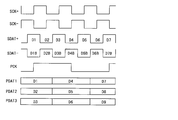
- FIG. 6 is a diagram simply showing waveforms of signals used for the serial interface and signals used for the parallel interface.
- FIG. 6 shows serial clock signals SCK + and SCK ⁇ , serial data signals SDAT + and SDAT ⁇ , a parallel clock signal PCK, and parallel data signals PDAT1 to PDAT3.
- the serial clock signal means a clock signal in a predetermined serial interface specification
- the serial data signal means a data signal in the specification
- the parallel clock signal means a clock signal in a predetermined parallel interface specification
- the parallel data signal means a data signal in the specification.
- FIG. 6 shows two serial data signals SDAT + and SDAT ⁇ for simplicity of explanation.
- An example in which three parallel data signals PDAT1 to PDAT3 are used will be described. Each data is sampled at both edges (rising time and falling time) of the corresponding clock, but may be sampled only at one edge.
- serial clock signals SCK + and SCK ⁇ and serial data signals SDAT + and SDAT ⁇ which are a positive signal and a negative signal, which are in a differential signal relationship.
- the voltage level here is 0.9V, which is half of 1.8V of the logic power supply voltage.
- the amplitude is ⁇ 100 mV.
- the data signal and the clock signal used for the serial interface have a small amplitude but a high frequency.
- the generation of EMI can be suppressed and high-speed data transmission is possible.
- power consumption increases for that purpose.
- the amplitudes of the parallel clock signal PCK and the parallel data signals PDAT1 to PDAT3 are 1.8V of the logic power supply voltage, the amplitude is large, and the frequency is also set low. . This enables data transmission with low power consumption. Further, in order to secure a necessary data transmission amount within a unit time, the number of signals (here, 24) larger than the number of signals used in the serial interface (here, 4) is required.
- the data signal and clock signal used for the serial interface have a high frequency and a small amplitude. Specifically, since the frequency is high, the signal setup time and hold time are shortened, resulting in low noise resistance, and because the amplitude is small, the voltage range in which the signal level can be recognized is reduced, so that noise resistance is also achieved. Becomes lower. For this reason, when an FPC board having a very small resistance value is used, these signals can be transmitted over a relatively long distance. However, as described above, the above signal is transmitted by the wiring on the glass substrate having a relatively large resistance value. In order to ensure sufficient noise resistance, these wirings are preferably as short as possible.
- the power supply line and the ground line are required to have as low impedance as possible for stable operation of the circuit. Therefore, when connecting a power supply line or a ground line by wiring on a glass substrate having a relatively large resistance value, it is preferable that these wirings are as short as possible.
- the data signal and clock signal used for the parallel interface have a low frequency and a large amplitude. Specifically, since the frequency is low, the signal setup time and hold time are increased, resulting in higher noise resistance. Also, because the amplitude is large, the voltage range in which the signal level can be recognized is increased, and the noise resistance is increased. Becomes higher. Therefore, even when an FPC board is used, and even when a wiring on a glass board having a relatively large resistance value is used, these signals can be transmitted over a relatively long distance as long as no malfunction occurs. .
- the upper limit value of the wiring impedance required for stable operation in the serial interface is smaller than the upper limit value of the wiring impedance required for stable operation in the parallel interface.
- each of the 24 data signal lines used for the parallel interface is arranged along the long side (of the LSI chip 140) on the display unit 130 side that is far from the FPC board 150. Connected to the 24 input terminals 141b.
- the length of the long side can be made smaller (by 1680 ⁇ m) than the conventional configuration in which all the input terminals of the LSI chip are arranged on the FPC board side without causing malfunction due to noise or the like.
- a configuration in which a part or all of the clock signal lines used for the parallel interface are connected to the 24 input terminals 141b may be employed. Further, a configuration may be adopted in which some or all of the synchronization signal lines used for the parallel interface (other signal lines excluding the power supply line and the ground line) are connected.
- the 24 input terminals 141b and 24 data signal lines are connected by a parallel data wiring 173a.
- the parallel data wiring 173a is disposed so as to pass directly under the short side (on the right side of the drawing) of the LSI chip 140.
- the parallel data wiring 173a may be routed outward so as not to pass directly under the LSI chip 140, but in that case, the parallel data wiring 173a becomes longer. In that case, since the impedance of the parallel data wiring 173a increases, a malfunction may occur depending on circumstances.
- the wiring (in this case, the parallel data wiring 173a) connected to the 24 input terminals 141b arranged along the long side on the display unit 130 side passes directly under the LSI chip 140 and has no terminals. It is preferable to be arranged so as to be drawn out under 140 short sides. However, the number of terminals drawn through directly under the chip short side may be limited by the chip short side size. In that case, some terminals may pass directly under the chip short side, and the remaining terminals may be routed outward.
- the 24 input terminals 141b are arranged in the vicinity of the short side of the LSI chip 140. If so, the parallel data wiring 173a can be shortened, so that the possibility of malfunctions can be reduced by reducing the impedance. Even if the parallel data wiring 173a is routed outward so as not to pass directly under the LSI chip 140, the parallel data wiring 173a can be provided by arranging the 24 input terminals 141b in the vicinity of the short side of the LSI chip 140. Can be shortened, which is preferable.
- the parallel data wiring 173a connected to the 24 input terminals 141b is formed to be wider than the various wirings 173b which are the other FPC wirings 173.
- some of the input terminals for the parallel interface are arranged along the long side on the display unit 130 side.
- the parallel interface signal for example, an input terminal for receiving the parallel clock signal PCK
- the same LSI chip 140 is mounted on two liquid crystal modules built in one portable information terminal (liquid crystal display device).
- the number is not particularly problematic when the present invention is applied, and any configuration may be used as long as the LSI chip 140 includes a serial interface input terminal and a parallel interface input terminal.
- the LSI chip 140 having the same configuration is used in these devices, the above embodiment is used. In the same way as in the case, the manufacturing cost can be reduced.
- the same LSI chip 140 is mounted on the glass substrate in each liquid crystal module.
- the display drive circuit is an area adjacent to the display unit on the glass substrate.
- a monolithic type formed using a thin film such as continuous grain boundary crystal silicon (CG silicon: ContinuousConGrain Silicon), amorphous silicon, or polycrystalline silicon may be employed.
- CG silicon ContinuousConGrain Silicon
- amorphous silicon or polycrystalline silicon
- the size is often increased depending on the process rule.
- the configuration of the first and second liquid crystal modules 110 and 210 before forming each wiring is the same. Therefore, the manufacturing cost can be similarly reduced.
- various wiring is formed on a glass substrate using tantalum (Ta) or aluminum (Al), other well-known wiring materials can be used.
- various wirings are formed on the glass substrate, but a transparent plastic substrate made of a known material may be used instead of the glass substrate which is a transparent substrate.
- various wiring materials can be used, but typically transparent ITO (indium tin oxide) is used.
- the substrate module which is a liquid crystal module has been described.
- the substrate module is not limited to the liquid crystal module used in the liquid crystal display device, and an organic or inorganic EL (Electro Luminescence) display, plasma display panel (Plasma Display Display; It can be similarly applied to substrate modules used in various display devices such as vacuum fluorescent display (Vacuum Fluorescent Display), electronic paper, etc., and similarly applied to various substrate modules used other than display devices. be able to.
- the present invention is applied to a display drive circuit and a board module such as a liquid crystal module provided with the display drive circuit, and more specifically, two or more types of input interface terminals used for a portable information terminal, for example. It is suitable for a display driving circuit having the above and a substrate module including the same.
Abstract
Description
第1のインタフェース仕様に基づく第1の信号を受け取るための第1の入力端子群と、
前記第1のインタフェース仕様よりも振幅値が小さいかまたは周波数が高い信号を使用する第2のインタフェース仕様に基づく第2の信号を受け取るための第2の入力端子群と、
前記第1および第2の信号の少なくとも一方に基づき生成される、前記画像を表示するための表示信号を前記表示部へ与えるための出力端子群と
を備え、
前記出力端子群と、前記第1の入力端子群の少なくとも一部とは、前記長辺の一方に沿って配列され、
前記第2の入力端子群は、前記長辺の他方に沿って配列されることを特徴とする。
前記第1の信号は、パラレルインタフェース仕様に基づくパラレルデータ信号およびパラレルクロック信号を含み、
前記第2の信号は、シリアルインタフェース仕様に基づくシリアルデータ信号およびシリアルクロック信号を含むことを特徴とする。
前記長辺の一方に沿って配列される前記第1の入力端子群は、前記パラレルデータ信号および前記パラレルクロック信号のうちの少なくとも一部を受け取るためのパラレル入力端子を含むことを特徴とする。
前記パラレル入力端子は、前記短辺の近傍に配置されることを特徴とする。
前記第1の入力端子群のうち、前記パラレルデータ信号および前記パラレルクロック信号のうちの少なくとも一部を受け取るためのパラレル入力端子は、前記短辺に沿って配置されることを特徴とする。
前記長辺の他方に沿って配列される前記第2の入力端子群は、前記シリアルデータ信号および前記シリアル信号を受け取るための入力端子を含むことを特徴とする。
透明基板と、
前記透明基板上に形成されており、前記出力端子群から前記表示部へ前記表示信号を伝送するための表示用配線と、
前記透明基板上に形成されており、外部から与えられる前記第1および第2の信号の少なくとも一方を、前記第1および第2の入力端子群の少なくとも一方へ伝送するための入力用配線と
を備え、
前記表示用駆動回路は、前記出力端子群が配置される長辺の一方が前記表示部に近接するよう配置されることを特徴とする。
前記第1の信号は、パラレルインタフェース仕様に基づくパラレルデータ信号およびパラレルクロック信号を含み、
前記第2の信号は、シリアルインタフェース仕様に基づくシリアルデータ信号およびシリアルクロック信号を含み、
前記長辺の一方に沿って配列される前記第1の入力端子群は、前記パラレルデータ信号および前記パラレルクロック信号のうちの少なくとも一部を受け取るためのパラレル入力端子を含むことを特徴とする。
前記表示用駆動回路は、前記透明基板上に回路チップとして取り付けられており、
前記パラレル入力端子は、前記短辺の近傍に配置され、
前記パラレル入力端子に接続される入力用配線は、前記回路チップの下側から前記短辺を通るよう配置されることを特徴とする。
前記パラレル入力端子に接続される入力用配線は、前記長辺の他方に沿って配列される前記第2の入力端子群に接続される入力配線よりも幅が大きいことを特徴とする。
図1は、本発明の一実施形態に係る液晶表示装置の構成を簡略に示す斜視図であり、図2はその構成を示す模式平面図である。図1に示されるように、この液晶表示装置は、PDA(Personal Digital Assistant)や携帯電話端末等の携帯情報端末であって、第1の液晶モジュール110およびメイン基板100と、これらを収納する第1の筐体101と、第2の液晶モジュール210と、これを収納する第2の筐体201とを備える。また、第1の液晶モジュール110とメイン基板100とは、第1のFPC基板150により接続されており、第2の液晶モジュール210とメイン基板100とは、第2のFPC基板250により接続されている。なお、これら各構成要素の配置位置や、大きさ、形状などは、見やすくするために実際とは異なるように記載されている。
図3は、本発明の一実施形態に係る第1の液晶モジュール110の構成を示す模式平面図であり、図4は、本発明の一実施形態に係る第2の液晶モジュール210の構成を示す模式平面図である。なお、これらの図中に示される各構成要素の配置位置や形状は、見やすくするために実際とは異なるように記載されている。
以上のように、LSIチップ140の入力端子のうちパラレルインタフェース用の入力端子の一部(ここではパラレルデータ信号を受け取る24の入力端子)と出力端子とが表示部130側の長辺に沿って配置され、残りのパラレルインタフェース用の入力端子がFPC基板150側の長辺に沿って配置される。この構成により、表示用駆動回路であるLSIチップ140の長辺の長さを(全入力端子が一列に配置されるときの長さよりも)小さくすることができ、その製造コストを下げることができる。
上記実施形態では、パラレルインタフェース用の入力端子の一部(ここではパラレルデータ信号を受け取る24の入力端子)が表示部130側の長辺に沿って配置されるが、これらの一部(またはその他のパラレルインタフェース用信号、例えばパラレルクロック信号PCKを受け取る入力端子)がLSIチップ140の短辺に沿って配置されてもよい。このような構成であっても表示用駆動回路であるLSIチップ140の長辺の長さを(全入力端子が一列に配置される長さよりも)小さくすることができるので、その製造コストを下げることができる。
101…第1の筐体
110…第1の液晶モジュール
120,125、220,225…ガラス基板
120a,220a…張出部
123,223…表示用配線
130,230…表示部
140…LSIチップ
141a…出力端子
141b…入力端子
150,250…FPC基板
173,273…FPC用配線
173a…パラレルデータ配線
174,274…FPC基板の配線層
201…第2の筐体
210…第2の液晶モジュール
Claims (10)
- 長辺と短辺とを有する矩形の形状を有しており、画像を表示する表示部を含む透明基板上に設けられるべき表示用駆動回路であって、
第1のインタフェース仕様に基づく第1の信号を受け取るための第1の入力端子群と、
前記第1のインタフェース仕様よりも振幅値が小さいかまたは周波数が高い信号を使用する第2のインタフェース仕様に基づく第2の信号を受け取るための第2の入力端子群と、
前記第1および第2の信号の少なくとも一方に基づき生成される、前記画像を表示するための表示信号を前記表示部へ与えるための出力端子群と
を備え、
前記出力端子群と、前記第1の入力端子群の少なくとも一部とは、前記長辺の一方に沿って配列され、
前記第2の入力端子群は、前記長辺の他方に沿って配列されることを特徴とする、表示用駆動回路。 - 前記第1の信号は、パラレルインタフェース仕様に基づくパラレルデータ信号およびパラレルクロック信号を含み、
前記第2の信号は、シリアルインタフェース仕様に基づくシリアルデータ信号およびシリアルクロック信号を含むことを特徴とする、請求項1に記載の表示用駆動回路。 - 前記長辺の一方に沿って配列される前記第1の入力端子群は、前記パラレルデータ信号および前記パラレルクロック信号のうちの少なくとも一部を受け取るためのパラレル入力端子を含むことを特徴とする、請求項2に記載の表示用駆動回路。
- 前記パラレル入力端子は、前記短辺の近傍に配置されることを特徴とする、請求項3に記載の表示用駆動回路。
- 前記第1の入力端子群のうち、前記パラレルデータ信号および前記パラレルクロック信号のうちの少なくとも一部を受け取るためのパラレル入力端子は、前記短辺に沿って配置されることを特徴とする、請求項2に記載の表示用駆動回路。
- 前記長辺の他方に沿って配列される前記第2の入力端子群は、前記シリアルデータ信号および前記シリアル信号を受け取るための入力端子を含むことを特徴とする、請求項2に記載の表示用駆動回路。
- 請求項1に記載の表示用駆動回路および表示部と、
透明基板と、
前記透明基板上に形成されており、前記出力端子群から前記表示部へ前記表示信号を伝送するための表示用配線と、
前記透明基板上に形成されており、外部から与えられる前記第1および第2の信号の少なくとも一方を、前記第1および第2の入力端子群の少なくとも一方へ伝送するための入力用配線と
を備え、
前記表示用駆動回路は、前記出力端子群が配置される長辺の一方が前記表示部に近接するよう配置されることを特徴とする、基板モジュール。 - 前記第1の信号は、パラレルインタフェース仕様に基づくパラレルデータ信号およびパラレルクロック信号を含み、
前記第2の信号は、シリアルインタフェース仕様に基づくシリアルデータ信号およびシリアルクロック信号を含み、
前記長辺の一方に沿って配列される前記第1の入力端子群は、前記パラレルデータ信号および前記パラレルクロック信号のうちの少なくとも一部を受け取るためのパラレル入力端子を含むことを特徴とする、請求項7に記載の基板モジュール。 - 前記表示用駆動回路は、前記透明基板上に回路チップとして取り付けられており、
前記パラレル入力端子は、前記短辺の近傍に配置され、
前記パラレル入力端子に接続される入力用配線は、前記回路チップの下側から前記短辺を通るよう配置されることを特徴とする、請求項8に記載の基板モジュール。 - 前記パラレル入力端子に接続される入力用配線は、前記長辺の他方に沿って配列される前記第2の入力端子群に接続される入力配線よりも幅が大きいことを特徴とする、請求項8に記載の基板モジュール。
Priority Applications (6)
| Application Number | Priority Date | Filing Date | Title |
|---|---|---|---|
| RU2011154110/08A RU2486577C1 (ru) | 2009-06-10 | 2010-05-12 | Схема управления дисплеем и одноплатный модуль, включающий в себя такую схему |
| EP10786020A EP2442293A4 (en) | 2009-06-10 | 2010-05-12 | DISPLAY CONTROL CIRCUIT AND SUBSTRATE MODULE THEREOF |
| US13/264,081 US9183805B2 (en) | 2009-06-10 | 2010-05-12 | Display driver circuit and board module including same |
| CN201080025609.4A CN102460541B (zh) | 2009-06-10 | 2010-05-12 | 显示用驱动电路和具备它的基板模块 |
| BRPI1012944A BRPI1012944A2 (pt) | 2009-06-10 | 2010-05-12 | "circuito de unidade de exibição e módulo de placa incluindo o mesmo" |
| JP2011518367A JP5307240B2 (ja) | 2009-06-10 | 2010-05-12 | 表示用駆動回路およびそれを備える基板モジュール |
Applications Claiming Priority (2)
| Application Number | Priority Date | Filing Date | Title |
|---|---|---|---|
| JP2009138923 | 2009-06-10 | ||
| JP2009-138923 | 2009-06-10 |
Publications (1)
| Publication Number | Publication Date |
|---|---|
| WO2010143489A1 true WO2010143489A1 (ja) | 2010-12-16 |
Family
ID=43308749
Family Applications (1)
| Application Number | Title | Priority Date | Filing Date |
|---|---|---|---|
| PCT/JP2010/057998 WO2010143489A1 (ja) | 2009-06-10 | 2010-05-12 | 表示用駆動回路およびそれを備える基板モジュール |
Country Status (7)
| Country | Link |
|---|---|
| US (1) | US9183805B2 (ja) |
| EP (1) | EP2442293A4 (ja) |
| JP (1) | JP5307240B2 (ja) |
| CN (1) | CN102460541B (ja) |
| BR (1) | BRPI1012944A2 (ja) |
| RU (1) | RU2486577C1 (ja) |
| WO (1) | WO2010143489A1 (ja) |
Cited By (1)
| Publication number | Priority date | Publication date | Assignee | Title |
|---|---|---|---|---|
| JP2011186076A (ja) * | 2010-03-05 | 2011-09-22 | Oki Semiconductor Co Ltd | 表示パネル |
Families Citing this family (8)
| Publication number | Priority date | Publication date | Assignee | Title |
|---|---|---|---|---|
| US20130328846A1 (en) * | 2012-06-08 | 2013-12-12 | Apple Inc. | Characterization of transistors on a display system substrate using a replica transistor |
| US9524683B2 (en) * | 2012-07-20 | 2016-12-20 | Sharp Kabushiki Kaisha | Display device with signal lines routed to decrease size of non-display area |
| KR20140079062A (ko) | 2012-12-18 | 2014-06-26 | 삼성전자주식회사 | 반도체 패키지 및 이를 이용한 표시 장치 |
| WO2014132799A1 (ja) * | 2013-02-26 | 2014-09-04 | シャープ株式会社 | 表示装置 |
| CN103676230B (zh) * | 2013-11-01 | 2017-01-11 | 六安市晶润光电科技有限公司 | 稳定电连接式液晶显示模块 |
| EP3185568A1 (en) * | 2015-12-23 | 2017-06-28 | Samsung Electronics Co., Ltd. | Display apparatus and control method for connecting external sources |
| US10388213B2 (en) * | 2017-05-22 | 2019-08-20 | Microsoft Technology Licensing, Llc | Display and display integration method |
| CN109976050B (zh) * | 2019-04-15 | 2024-01-26 | 武汉华星光电技术有限公司 | 显示面板及适用于该显示面板的芯片 |
Citations (4)
| Publication number | Priority date | Publication date | Assignee | Title |
|---|---|---|---|---|
| JPH0179137U (ja) * | 1987-11-13 | 1989-05-26 | ||
| JP2005242017A (ja) * | 2004-02-26 | 2005-09-08 | Optrex Corp | 液晶表示パネル及び液晶表示装置 |
| JP2006330551A (ja) * | 2005-05-30 | 2006-12-07 | Renesas Technology Corp | 液晶駆動制御装置、携帯端末システム及びデータ処理システム |
| JP2010122483A (ja) * | 2008-11-20 | 2010-06-03 | Epson Imaging Devices Corp | 電気光学パネル、電気光学装置、および電子機器 |
Family Cites Families (11)
| Publication number | Priority date | Publication date | Assignee | Title |
|---|---|---|---|---|
| CA2051655C (en) * | 1990-02-05 | 1997-04-22 | Toyofumi Takahashi | Animation display unit and external memory used therefor |
| US5249218A (en) * | 1992-04-06 | 1993-09-28 | Spectrum Information Technologies, Inc. | Programmable universal interface system |
| JP4204685B2 (ja) * | 1999-01-19 | 2009-01-07 | 株式会社ルネサステクノロジ | 同期型半導体記憶装置 |
| JP3892650B2 (ja) * | 2000-07-25 | 2007-03-14 | 株式会社日立製作所 | 液晶表示装置 |
| JP2003107513A (ja) * | 2001-09-27 | 2003-04-09 | Citizen Watch Co Ltd | 液晶表示装置 |
| KR100831235B1 (ko) * | 2002-06-07 | 2008-05-22 | 삼성전자주식회사 | 박막 트랜지스터 기판 |
| US20070038782A1 (en) * | 2005-07-26 | 2007-02-15 | Ambric, Inc. | System of virtual data channels across clock boundaries in an integrated circuit |
| JP2006106077A (ja) * | 2004-09-30 | 2006-04-20 | Seiko Epson Corp | 電気光学装置及び電子機器 |
| US7184360B2 (en) * | 2005-06-15 | 2007-02-27 | Infineon Technologies, Ag | High-speed interface circuit for semiconductor memory chips and memory system including semiconductor memory chips |
| KR100987479B1 (ko) * | 2005-12-19 | 2010-10-13 | 삼성전자주식회사 | 반도체 칩 및 이를 이용한 반도체 칩 패키지 |
| JP4370321B2 (ja) * | 2006-12-05 | 2009-11-25 | 株式会社沖データ | 駆動装置、ledアレイ、ledヘッド、及びこれらを備えた画像形成装置 |
-
2010
- 2010-05-12 CN CN201080025609.4A patent/CN102460541B/zh not_active Expired - Fee Related
- 2010-05-12 JP JP2011518367A patent/JP5307240B2/ja not_active Expired - Fee Related
- 2010-05-12 RU RU2011154110/08A patent/RU2486577C1/ru not_active IP Right Cessation
- 2010-05-12 BR BRPI1012944A patent/BRPI1012944A2/pt not_active IP Right Cessation
- 2010-05-12 US US13/264,081 patent/US9183805B2/en not_active Expired - Fee Related
- 2010-05-12 EP EP10786020A patent/EP2442293A4/en not_active Withdrawn
- 2010-05-12 WO PCT/JP2010/057998 patent/WO2010143489A1/ja active Application Filing
Patent Citations (4)
| Publication number | Priority date | Publication date | Assignee | Title |
|---|---|---|---|---|
| JPH0179137U (ja) * | 1987-11-13 | 1989-05-26 | ||
| JP2005242017A (ja) * | 2004-02-26 | 2005-09-08 | Optrex Corp | 液晶表示パネル及び液晶表示装置 |
| JP2006330551A (ja) * | 2005-05-30 | 2006-12-07 | Renesas Technology Corp | 液晶駆動制御装置、携帯端末システム及びデータ処理システム |
| JP2010122483A (ja) * | 2008-11-20 | 2010-06-03 | Epson Imaging Devices Corp | 電気光学パネル、電気光学装置、および電子機器 |
Non-Patent Citations (1)
| Title |
|---|
| See also references of EP2442293A4 * |
Cited By (3)
| Publication number | Priority date | Publication date | Assignee | Title |
|---|---|---|---|---|
| JP2011186076A (ja) * | 2010-03-05 | 2011-09-22 | Oki Semiconductor Co Ltd | 表示パネル |
| US9185817B2 (en) | 2010-03-05 | 2015-11-10 | Lapis Semiconductor Co., Ltd. | Display panel |
| US10109256B2 (en) | 2010-03-05 | 2018-10-23 | Lapis Semiconductor Co., Ltd. | Display panel |
Also Published As
| Publication number | Publication date |
|---|---|
| US20120026138A1 (en) | 2012-02-02 |
| EP2442293A4 (en) | 2012-10-17 |
| CN102460541B (zh) | 2014-08-20 |
| US9183805B2 (en) | 2015-11-10 |
| RU2486577C1 (ru) | 2013-06-27 |
| BRPI1012944A2 (pt) | 2018-01-16 |
| JPWO2010143489A1 (ja) | 2012-11-22 |
| CN102460541A (zh) | 2012-05-16 |
| EP2442293A1 (en) | 2012-04-18 |
| JP5307240B2 (ja) | 2013-10-02 |
Similar Documents
| Publication | Publication Date | Title |
|---|---|---|
| JP5307240B2 (ja) | 表示用駆動回路およびそれを備える基板モジュール | |
| KR100453306B1 (ko) | 표시 소자 구동 장치 및 이를 이용한 표시 장치 | |
| US7683471B2 (en) | Display driver integrated circuit device, film, and module | |
| US20110169792A1 (en) | Display panel | |
| JP2008015507A (ja) | 表示基板及びそれを具備した表示装置 | |
| JP4997593B2 (ja) | 表示装置 | |
| WO2017045358A1 (zh) | 柔性基板和显示装置 | |
| JP2004062201A (ja) | ゲートpcb及びfpcがない液晶表示装置 | |
| US20110169791A1 (en) | Display device | |
| KR20120052764A (ko) | 칩 온 필름 및 이를 포함하는 액정표시장치 | |
| US20070081117A1 (en) | Display device and a circuit thereon | |
| WO2012006804A1 (zh) | 液晶显示器及其线路架构 | |
| US11877483B2 (en) | Display device with circuit film coupled to lateral surface of base substrate | |
| JP2002311451A (ja) | 電極駆動装置及び電子機器 | |
| KR101931338B1 (ko) | 연성회로기판과 이를 이용한 표시장치 | |
| CN212782503U (zh) | 显示装置和电子设备 | |
| CN114677987A (zh) | 一种显示面板及显示装置 | |
| WO2021253397A1 (zh) | 显示模组和显示装置 | |
| CN101359106A (zh) | 显示面板及其应用 | |
| CN113870691A (zh) | 显示装置和电子设备 | |
| WO2020220466A1 (zh) | 印刷电路板及显示装置 | |
| JP6334851B2 (ja) | 半導体装置、表示デバイスモジュール、及び、表示デバイスモジュールの製造方法 | |
| WO2024040405A1 (zh) | 一种阵列基板、显示面板及显示装置 | |
| WO2023103052A1 (zh) | 阵列基板与显示装置 | |
| JPH11126792A (ja) | フェースダウン用多出力ドライバの電極位置,フェースダウン用icの電極位置,配線基板およびディスプレイモジュール |
Legal Events
| Date | Code | Title | Description |
|---|---|---|---|
| WWE | Wipo information: entry into national phase |
Ref document number: 201080025609.4 Country of ref document: CN |
|
| 121 | Ep: the epo has been informed by wipo that ep was designated in this application |
Ref document number: 10786020 Country of ref document: EP Kind code of ref document: A1 |
|
| ENP | Entry into the national phase |
Ref document number: 2011518367 Country of ref document: JP Kind code of ref document: A |
|
| WWE | Wipo information: entry into national phase |
Ref document number: 13264081 Country of ref document: US |
|
| WWE | Wipo information: entry into national phase |
Ref document number: 2010786020 Country of ref document: EP |
|
| NENP | Non-entry into the national phase |
Ref country code: DE |
|
| WWE | Wipo information: entry into national phase |
Ref document number: 243/CHENP/2012 Country of ref document: IN |
|
| WWE | Wipo information: entry into national phase |
Ref document number: 2011154110 Country of ref document: RU |
|
| REG | Reference to national code |
Ref country code: BR Ref legal event code: B01A Ref document number: PI1012944 Country of ref document: BR |
|
| ENP | Entry into the national phase |
Ref document number: PI1012944 Country of ref document: BR Kind code of ref document: A2 Effective date: 20111209 |