WO2010134494A2 - 多層ポリエステルフィルム - Google Patents
多層ポリエステルフィルム Download PDFInfo
- Publication number
- WO2010134494A2 WO2010134494A2 PCT/JP2010/058299 JP2010058299W WO2010134494A2 WO 2010134494 A2 WO2010134494 A2 WO 2010134494A2 JP 2010058299 W JP2010058299 W JP 2010058299W WO 2010134494 A2 WO2010134494 A2 WO 2010134494A2
- Authority
- WO
- WIPO (PCT)
- Prior art keywords
- touch panel
- adhesive layer
- panel sheet
- film
- adhesive
- Prior art date
- Legal status (The legal status is an assumption and is not a legal conclusion. Google has not performed a legal analysis and makes no representation as to the accuracy of the status listed.)
- Ceased
Links
Images





Classifications
-
- G—PHYSICS
- G06—COMPUTING OR CALCULATING; COUNTING
- G06F—ELECTRIC DIGITAL DATA PROCESSING
- G06F3/00—Input arrangements for transferring data to be processed into a form capable of being handled by the computer; Output arrangements for transferring data from processing unit to output unit, e.g. interface arrangements
- G06F3/01—Input arrangements or combined input and output arrangements for interaction between user and computer
- G06F3/03—Arrangements for converting the position or the displacement of a member into a coded form
- G06F3/041—Digitisers, e.g. for touch screens or touch pads, characterised by the transducing means
-
- B—PERFORMING OPERATIONS; TRANSPORTING
- B32—LAYERED PRODUCTS
- B32B—LAYERED PRODUCTS, i.e. PRODUCTS BUILT-UP OF STRATA OF FLAT OR NON-FLAT, e.g. CELLULAR OR HONEYCOMB, FORM
- B32B15/00—Layered products comprising a layer of metal
- B32B15/04—Layered products comprising a layer of metal comprising metal as the main or only constituent of a layer, which is next to another layer of the same or of a different material
- B32B15/08—Layered products comprising a layer of metal comprising metal as the main or only constituent of a layer, which is next to another layer of the same or of a different material of synthetic resin
-
- B—PERFORMING OPERATIONS; TRANSPORTING
- B32—LAYERED PRODUCTS
- B32B—LAYERED PRODUCTS, i.e. PRODUCTS BUILT-UP OF STRATA OF FLAT OR NON-FLAT, e.g. CELLULAR OR HONEYCOMB, FORM
- B32B27/00—Layered products comprising a layer of synthetic resin
- B32B27/06—Layered products comprising a layer of synthetic resin as the main or only constituent of a layer, which is next to another layer of the same or of a different material
- B32B27/08—Layered products comprising a layer of synthetic resin as the main or only constituent of a layer, which is next to another layer of the same or of a different material of synthetic resin
-
- B—PERFORMING OPERATIONS; TRANSPORTING
- B32—LAYERED PRODUCTS
- B32B—LAYERED PRODUCTS, i.e. PRODUCTS BUILT-UP OF STRATA OF FLAT OR NON-FLAT, e.g. CELLULAR OR HONEYCOMB, FORM
- B32B27/00—Layered products comprising a layer of synthetic resin
- B32B27/36—Layered products comprising a layer of synthetic resin comprising polyesters
-
- B—PERFORMING OPERATIONS; TRANSPORTING
- B32—LAYERED PRODUCTS
- B32B—LAYERED PRODUCTS, i.e. PRODUCTS BUILT-UP OF STRATA OF FLAT OR NON-FLAT, e.g. CELLULAR OR HONEYCOMB, FORM
- B32B7/00—Layered products characterised by the relation between layers; Layered products characterised by the relative orientation of features between layers, or by the relative values of a measurable parameter between layers, i.e. products comprising layers having different physical, chemical or physicochemical properties; Layered products characterised by the interconnection of layers
- B32B7/04—Interconnection of layers
- B32B7/12—Interconnection of layers using interposed adhesives or interposed materials with bonding properties
-
- B—PERFORMING OPERATIONS; TRANSPORTING
- B32—LAYERED PRODUCTS
- B32B—LAYERED PRODUCTS, i.e. PRODUCTS BUILT-UP OF STRATA OF FLAT OR NON-FLAT, e.g. CELLULAR OR HONEYCOMB, FORM
- B32B9/00—Layered products comprising a layer of a particular substance not covered by groups B32B11/00 - B32B29/00
- B32B9/005—Layered products comprising a layer of a particular substance not covered by groups B32B11/00 - B32B29/00 comprising one layer of ceramic material, e.g. porcelain, ceramic tile
-
- B—PERFORMING OPERATIONS; TRANSPORTING
- B32—LAYERED PRODUCTS
- B32B—LAYERED PRODUCTS, i.e. PRODUCTS BUILT-UP OF STRATA OF FLAT OR NON-FLAT, e.g. CELLULAR OR HONEYCOMB, FORM
- B32B9/00—Layered products comprising a layer of a particular substance not covered by groups B32B11/00 - B32B29/00
- B32B9/04—Layered products comprising a layer of a particular substance not covered by groups B32B11/00 - B32B29/00 comprising such particular substance as the main or only constituent of a layer, which is next to another layer of the same or of a different material
- B32B9/045—Layered products comprising a layer of a particular substance not covered by groups B32B11/00 - B32B29/00 comprising such particular substance as the main or only constituent of a layer, which is next to another layer of the same or of a different material of synthetic resin
-
- B—PERFORMING OPERATIONS; TRANSPORTING
- B32—LAYERED PRODUCTS
- B32B—LAYERED PRODUCTS, i.e. PRODUCTS BUILT-UP OF STRATA OF FLAT OR NON-FLAT, e.g. CELLULAR OR HONEYCOMB, FORM
- B32B2255/00—Coating on the layer surface
- B32B2255/10—Coating on the layer surface on synthetic resin layer or on natural or synthetic rubber layer
-
- B—PERFORMING OPERATIONS; TRANSPORTING
- B32—LAYERED PRODUCTS
- B32B—LAYERED PRODUCTS, i.e. PRODUCTS BUILT-UP OF STRATA OF FLAT OR NON-FLAT, e.g. CELLULAR OR HONEYCOMB, FORM
- B32B2255/00—Coating on the layer surface
- B32B2255/20—Inorganic coating
-
- B—PERFORMING OPERATIONS; TRANSPORTING
- B32—LAYERED PRODUCTS
- B32B—LAYERED PRODUCTS, i.e. PRODUCTS BUILT-UP OF STRATA OF FLAT OR NON-FLAT, e.g. CELLULAR OR HONEYCOMB, FORM
- B32B2307/00—Properties of the layers or laminate
- B32B2307/30—Properties of the layers or laminate having particular thermal properties
- B32B2307/308—Heat stability
-
- B—PERFORMING OPERATIONS; TRANSPORTING
- B32—LAYERED PRODUCTS
- B32B—LAYERED PRODUCTS, i.e. PRODUCTS BUILT-UP OF STRATA OF FLAT OR NON-FLAT, e.g. CELLULAR OR HONEYCOMB, FORM
- B32B2307/00—Properties of the layers or laminate
- B32B2307/40—Properties of the layers or laminate having particular optical properties
- B32B2307/412—Transparent
-
- B—PERFORMING OPERATIONS; TRANSPORTING
- B32—LAYERED PRODUCTS
- B32B—LAYERED PRODUCTS, i.e. PRODUCTS BUILT-UP OF STRATA OF FLAT OR NON-FLAT, e.g. CELLULAR OR HONEYCOMB, FORM
- B32B2307/00—Properties of the layers or laminate
- B32B2307/50—Properties of the layers or laminate having particular mechanical properties
-
- B—PERFORMING OPERATIONS; TRANSPORTING
- B32—LAYERED PRODUCTS
- B32B—LAYERED PRODUCTS, i.e. PRODUCTS BUILT-UP OF STRATA OF FLAT OR NON-FLAT, e.g. CELLULAR OR HONEYCOMB, FORM
- B32B2307/00—Properties of the layers or laminate
- B32B2307/70—Other properties
- B32B2307/732—Dimensional properties
- B32B2307/734—Dimensional stability
- B32B2307/736—Shrinkable
-
- B—PERFORMING OPERATIONS; TRANSPORTING
- B32—LAYERED PRODUCTS
- B32B—LAYERED PRODUCTS, i.e. PRODUCTS BUILT-UP OF STRATA OF FLAT OR NON-FLAT, e.g. CELLULAR OR HONEYCOMB, FORM
- B32B2457/00—Electrical equipment
- B32B2457/20—Displays, e.g. liquid crystal displays, plasma displays
- B32B2457/202—LCD, i.e. liquid crystal displays
-
- B—PERFORMING OPERATIONS; TRANSPORTING
- B32—LAYERED PRODUCTS
- B32B—LAYERED PRODUCTS, i.e. PRODUCTS BUILT-UP OF STRATA OF FLAT OR NON-FLAT, e.g. CELLULAR OR HONEYCOMB, FORM
- B32B2457/00—Electrical equipment
- B32B2457/20—Displays, e.g. liquid crystal displays, plasma displays
- B32B2457/208—Touch screens
Definitions
- the present invention relates to a technical field of a touch panel using a multilayer conductive transparent film, and particularly relates to a technique for suppressing precipitation of oligomers in an adhesive layer.
- This application is based on Japanese Patent Application No. 2009-120332 filed on May 18, 2009 in Japan and Japanese Patent Application No. 2009-136530 filed on June 5, 2009. Priority is claimed and is incorporated into this application by reference to these applications.
- the transparent conductive electrode used for the touch panel has a three-layer multilayer film in which an adhesive layer made of an acrylic resin is disposed between two film-like PET (polyethylene terephthalate), and further on one PET surface. A hard coat layer is formed, and a transparent electrically conductive thin film made of ITO or the like is formed on the other PET surface to form a touch panel sheet.
- this touch panel sheet is subjected to a pre-annealing process for causing thermal shrinkage of PET in advance so that the touch panel sheet is not thermally deformed even if it is annealed in the manufacturing process of the touch panel.
- the diffusion of the oligomer contained in the PET proceeds, and the diffused oligomer is precipitated at the interface between the PET and the adhesive, so that it is not compatible with the adhesive and crystallizes. There was a problem that it turned into cloudy.
- oligomers are deposited by forming a coating layer composed of a polyester resin on at least one surface of a laminated polyester film, a compound having an acetylene group and a hydroxyl group in the molecule, and mineral oil. Suppressed.
- Non-Patent Document 1 oligomer deposition is suppressed by forming a special coating layer on the PET surface.
- a first resin film made of polyethylene terephthalate, an adhesive layer made of polyester disposed on the surface of the first resin film, and disposed on the surface of the adhesive layer A multilayer polyester film having a second resin film made of polyethylene terephthalate, wherein the first and second resin films are bonded with the adhesive layer, and the multilayer polyester film is heat-treated and used for a touch panel. It is a multilayer polyester film used as a sheet.
- the first and second resin films are obtained by polymerizing terephthalic acid and ethylene glycol
- the adhesive layer is a multilayer polyester film made of an adhesive containing terephthalic acid and ethylene glycol.
- This invention is a multilayer polyester film whose glass transition temperature of the said adhesive bond layer is less than 65 degreeC.
- the present invention provides a multilayer polyester film according to any one of claims 1 to 3, a first transparent conductive thin film made of indium tin oxide disposed on the back surface of the first resin film, And a protective layer disposed on the surface of the second resin film, wherein at least the multilayer polyester film is heated at a temperature of 140 ° C. or higher and is an upper touch panel sheet used on a pressed surface side of the touch panel. .
- the present invention includes an upper touch panel sheet and a lower touch panel sheet having a second transparent conductive thin film, wherein the upper touch panel sheet and the lower touch panel sheet are the first and second transparent conductive thin films.
- the upper touch panel sheet when the upper touch panel sheet is pressed so as to face and be separated, the upper touch panel sheet is curved, and the first transparent conductive thin film of the upper touch panel sheet is It is a touch panel in which a current flows in contact with the second transparent conductive thin film of the side touch panel sheet and a position in the contacted surface is required.
- the present invention is the touch panel in which the Young's modulus of the adhesive layer of the upper touch panel sheet is 1.5 MPa or more and 3.0 MPa or less.
- the present invention is the touch panel in which the adhesive layer of the upper touch panel sheet contains a curing agent that reacts at room temperature.
- the present invention includes a touch panel and a liquid crystal display device, and the touch panel is a touch panel with a liquid crystal disposed on the liquid crystal display device.
- an adhesive is placed in contact between the first and second resin films, and the temperature of the adhesive is raised to a temperature of less than 140 ° C.
- Two resin films are bonded to create a multilayer polyester film, a transparent conductive thin film is disposed on the surface of the first resin film opposite to the surface on which the adhesive is disposed, and the second resin
- this heating process is after a multilayer polyester film is made until it arrange
- the adhesive represents an adhesive layer and an adhesive film described later.
- the adhesive layer of the upper touch panel sheet of the present invention has an adhesive strength for bonding PET to each other, and the oligomer in the adhesive layer can be formed without forming a coating layer or a coating layer on the PET surface on the adhesive layer side. Even if it is not mixed with the adhesive layer and is not crystallized or not mixed, the refractive index of the light of the oligomer and the adhesive layer is almost the same, so it is not visually observed, so the touch panel sheet manufacturing process and cost can be reduced. .
- FIG. 1 is a cross-sectional view of the first resin film.
- FIG. 2 is a cross-sectional view of the first resin film and the adhesive layer disposed on the first resin film.
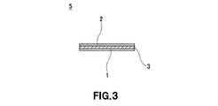
- FIG. 3 is a cross-sectional view of the multilayer polyester film of the present invention.
- FIG. 4 is a cross-sectional view of the touch panel sheet of the present invention.
- FIG. 5 is a cross-sectional view of the upper touch panel sheet of the present invention.
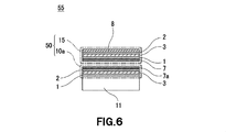
- FIG. 6 is a cross-sectional view of the touch panel with a liquid crystal display according to the present invention.
- FIG. 7 is a view for explaining a method for producing the multilayer polyester film of the present invention using the first and second resin film rolls and the adhesive film roll.
- 1 is a first resin film made of PET (polyethylene terephthalate), which is a process object.
- PET polyethylene terephthalate
- the multilayer transparent conductive sheet 10 is formed. (FIG. 4).
- the transparent conductive thin film formed into a film is not limited to ITO, What is necessary is just transparent electrodes, such as a tin oxide and a zinc oxide.
- the surface of the second resin film 2 of the multilayer transparent conductive sheet 10 is coated with a resin paint containing an inorganic filler such as silicon nitride, alumina, silica, titanium oxide, etc., and the temperature of the solution rises above the evaporation temperature of the solvent.
- a resin paint containing an inorganic filler such as silicon nitride, alumina, silica, titanium oxide, etc.
- the hard coat layer 8 is formed as a protective layer on the surface of the second resin film 2, and the upper touch panel sheet 15 is formed (FIG. 5).
- the order of laminating the first and second resin films 1 and 2 through the adhesive layer 3 and the timing for forming the first transparent conductive thin film 7 and the hard coat layer 8 are within the scope of the object of the present invention. Can be selected arbitrarily.
- ⁇ Heat treatment> When the upper touch panel sheet 15 is subjected to an annealing process for drying at a temperature of about 140 ° C. or higher in the touch panel manufacturing process, the first and second resin films 1 and 2 of the upper touch panel sheet 15 are thermally shrunk to the first. The wiring printed on the screen on the transparent conductive thin film 7 is distorted. In order to prevent thermal shrinkage during the annealing process, a pre-annealing process is performed in which the upper touch panel sheet 15 is heated in advance to heat-shrink the first and second resin films 1 and 2 before the wiring is printed.
- the upper touch panel sheet 15 When the upper touch panel sheet 15 is heated to 140 ° C. or higher by the pre-annealing process, it exceeds 110 ° C., which is the glass transition temperature of the first and second resin films 1 and 2. 2, the diffusion of the oligomer contained in 2 proceeds.
- the oligomer moves from the first and second resin films 1 and 2 to the adhesive layer 3 through the interface between the first and second resin films 1 and 2 and the adhesive layer 3. Crystallization does not proceed by mixing with polyester which is a component of the agent layer 3.
- the oligomer and the adhesive layer 3 are both polyester components, the refractive index of light is substantially equal, and even if it is crystallized, it is difficult to visually observe the portion.
- the adhesive strength of the adhesive layer 3 bonded to the first and second resin films 1 and 2 does not decrease even at a temperature of 140 ° C. or higher.
- the multilayer polyester film 5 is more flexible than a single PET film having the same thickness as the total thickness of the first and second resin films 1 and 2 and the adhesive layer 3.
- the touch panel 50 includes the upper touch panel sheet 15 and the multilayer transparent conductive sheet 10.
- the multilayer transparent conductive sheet 10 is used as the lower touch panel sheet 10a.
- the upper touch panel sheet 15 and the lower touch panel sheet 10a are separated so that the first transparent conductive thin film 7 of the upper touch panel sheet 15 and the second transparent conductive thin film 7a of the lower touch panel sheet 10a face each other. Arranged.
- FIG. 6 shows a liquid crystal touch panel 55 in which a touch panel 50 is arranged on the liquid crystal display device 11.
- the upper touch panel sheet 15 When a voltage is applied to the first and second transparent conductive thin films 7 and 7a and the hard coat layer 8 of the upper touch panel sheet 15 is pressed with a pen or a finger, the upper touch panel sheet 15 is bent and the upper touch panel sheet.
- the first transparent conductive thin film 7 of 15 and the second transparent conductive thin film 7a of the lower touch panel sheet 10a come into contact with each other, a current flows, and the position in the plane of the contact point is obtained.
- the upper touch panel sheet 15 Since the upper touch panel sheet 15 has flexibility and impact resistance even when pressed, the upper touch panel sheet 15 bends even when pressed at the edge of the screen window of the upper touch panel sheet 15, and the first transparent conductive material of the upper touch panel sheet 15.
- the conductive thin film 7 and the second transparent conductive thin film 7a of the lower touch panel sheet 10a come into contact with each other, a current flows and the position in the surface is obtained.
- symbol 20 of FIG. 7 is a multilayer polyester roll manufacturing apparatus, the 1st, 2nd resin film rolls 21 and 22, the adhesive bond layer application part 23, the 1st, 2nd bonding rolls 24 and 25, And a winding device 26.
- the first and second resin film rolls 21 and 22 are wound with the first and second resin films 31 and 32 made of PET, and the polyester containing terephthalic acid and ethylene glycol from the adhesive layer coating portion 23.
- a solution containing a system adhesive is applied onto the first resin film 31 and the solvent is evaporated to form the adhesive layer 33.
- the first and second resin film rolls 21 and 22 and the adhesive layer application part 23 are arranged in front of the first and second bonding rolls 24 and 25, and the winding device 26 includes the first and second It arrange
- first and second resin films 31 and 32 are pulled out from the first and second resin film rolls 21 and 22, and the adhesive layer 33 is applied and formed on the first resin film 31 by the adhesive layer application part 23.
- the first and second laminating rolls 24 and 25 are passed between the first and second bonding rolls 24 and 25 so as to be wound around the winding device 26.
- the first resin film roll 21, the adhesive layer application part 23, and the second resin film roll 22 are arranged in this order from the bottom, and the tips of the first and second resin films 31 and 32 are arranged.
- the take-up device 26 is held and the take-up device 26 is operated, the first and second resin films 31 and 32 are pulled out from the first and second resin film rolls 21 and 22, and the adhesive layer 33. Is applied and formed on the first resin film 31 from the adhesive layer application part 23.
- the drawn first and second resin films 31 and 32 are provided between the first and second laminating rolls 24 and 25 and the adhesive layer 33 formed on the first resin film 31 is interposed between them. And sandwiched between them.
- the first and second resin films 31 and 32 bonded together through the adhesive layer 33 become a multilayer polyester film 35.
- a multilayer polyester film roll 39 is obtained.
- the adhesive layer 3 was formed by changing the compounding ratio of the polyester resins A, B, and C having a glass transition temperature of 5 ° C., 65 ° C., and ⁇ 20 ° C. and the curing agent, and the adhesive layer 3 Young's modulus and glass transition temperature (Tg) were measured. Also, the first and second resin films 1 and 2 are bonded to each other through the adhesive layer 3 to create a multilayer polyester film 5, and the multilayer polyester film 5 is pre-annealed at a temperature of 140 ° C. or higher.
- the adhesive layer 3 is formed by changing the compounding ratio of the polyester resin B, the acrylic resin, and the photoinitiator, and the first and second resin films 1 are interposed via the adhesive layer 3. 2 and after pre-annealing at a temperature of 140 ° C. or higher, the generation of oligomers in the adhesive layer is evaluated, a 180 degree peel strength test is performed, and the adhesive layer 3 and the first and second resins The adhesive strength and impact resistance with the films 1 and 2 were examined.
- Table 1 showing the relationship between the Young's modulus and glass transition temperature of the adhesive layer 3 relative to the adhesive layer 3, the investigation of the occurrence of oligomers in the adhesive layer, the adhesive strength of the multilayer polyester film 5, and the impact resistance was obtained.
- ⁇ Oligomer generation evaluation> The size of the oligomer generated in the adhesive layer 3 was observed at a magnification of 1000 using a digital microscope (manufactured by KEYENCE). When the largest of the generated oligomers is observed with a maximum diameter of less than 5 ⁇ m, the largest one of the generated oligomers with a maximum diameter of 5 ⁇ m or more is observed as ⁇ (preferred) X (not preferable).
- the evaluation of the generation of oligomers in Examples 1 to 6 is preferable.
- the oligomer is mixed with polyester as a component of the adhesive layer 3 so that crystallization does not proceed, or both the oligomer and the adhesive layer 3 are polyester. Therefore, even if it is crystallized, it is difficult to visually check that portion.
- the Young's modulus of the adhesive layer 3 of Example 2 is larger than the Young's modulus of the adhesive layer 3 of Example 1 due to the addition of the curing agent isocyanate. Thus, even if a hardening
- the glass transition temperature of the adhesive layer 3 of Example 5 is lower than that of the other examples, the adhesive strength and the impact resistance are compatible.
- Example 6 the impact resistance is jerky peeling, and the impact resistance of the adhesive layer 3 is weak compared to the impact resistance of Examples 1 to 5, so that it can be used as the upper touch panel sheet 15. Although it is not possible, since the evaluation of oligomer generation and the adhesive strength are preferable, it can be used as the lower touch panel sheet 10a.
- Example 6 the evaluation of oligomer generation is preferable, and the Young's modulus exceeds 3.0 MPa, which is larger than Examples 1 to 5, but is used as the lower touch panel sheet 10a because the adhesive strength is maintained. You can see that you can.
- Comparative Example 2 although a polyester resin is used for the adhesive layer 3, the glass transition temperature is higher than that in Examples 1 to 6, so that the adhesive strength and impact resistance are not preferable.
- the Young's modulus and glass transition temperature of the adhesive layer of Comparative Example 3 are within the preferred ranges of the Young's modulus and glass transition temperature of Examples 1 to 5, the maximum diameter of the generated oligomers is the largest. Since the thing of 5 micrometers or more was observed, since it may be visually observed, it is not preferable.
- the Young's modulus of the adhesive layer 3 of the upper touch panel sheet 15 is preferably in the range of 1.5 MPa to 3.0 MPa, and the adhesive layers of the upper touch panel sheet 15 and the lower touch panel sheet 10a.
- the glass transition temperature of 3 indicates that a range of less than 65 ° C. is preferable.
Landscapes
- Engineering & Computer Science (AREA)
- Ceramic Engineering (AREA)
- General Engineering & Computer Science (AREA)
- Theoretical Computer Science (AREA)
- Chemical & Material Sciences (AREA)
- Human Computer Interaction (AREA)
- Physics & Mathematics (AREA)
- General Physics & Mathematics (AREA)
- Laminated Bodies (AREA)
- Position Input By Displaying (AREA)
Abstract
接着剤層側のPET表面に塗布層やコーティング層を形成しなくてもオリゴマの析出を抑制する透明電極シートを提供する。タッチパネルシートは、製造工程においてアニール処理される場合の熱収縮を防ぐために、アニール処理をする前に予め第一、第二の樹脂フィルム(1)、(2)を熱収縮させてプレアニール処理が行われる。プレアニール処理により第一、第二の樹脂フィルム(1)、(2)はガラス転移温度程度以上になると、第一、第二の樹脂フィルム(1)、(2)の中のオリゴマは析出し、拡散する。第一、第二の樹脂フィルム(1)、(2)から第一、第二の樹脂フィルム(1)、(2)と接着剤層(3)との界面を通過して、接着剤層(3)へ移動するオリゴマは、テレフタール酸とエチレングリコールを含有するポリエチレンから成る接着剤層(3)と混和して結晶として析出されない。オリゴマは、接着剤層(3)と混和しなくても、オリゴマと接着剤層(3)の光の屈折率が略等しいので目視されない。
Description
本発明は、多層導電性透明フィルムを用いるタッチパネルの技術分野にかかり、特に、接着剤層中のオリゴマの析出を抑制する技術に関する。
本出願は、日本国において2009年5月18日に出願された日本特許出願番号特願2009-120332、及び2009年6月5日に出願された日本特許出願番号特願2009-136530を基礎として優先権を主張するものであり、これらの出願を参照することにより、本出願に援用される。
本出願は、日本国において2009年5月18日に出願された日本特許出願番号特願2009-120332、及び2009年6月5日に出願された日本特許出願番号特願2009-136530を基礎として優先権を主張するものであり、これらの出願を参照することにより、本出願に援用される。
タッチパネルに用いられる透明導電性電極は、二つのフィルム状のPET(ポリエチレンテレフタレート)の間にアクリル系樹脂から成る接着剤層が配置された三層の多層フィルムを有し、さらに一方のPET表面にハードコート層を形成し、他方のPET表面にITO等から成る透明な電気導電性薄膜が形成されてタッチパネルシートとなる。通常、このタッチパネルシートは、タッチパネルの製造工程においてアニール処理されても熱変形しないように、予め、PETの熱収縮をさせるためのプレアニール処理を行う。プレアニールの処理温度がPETのガラス転移温度を超える場合、PET中に含まれるオリゴマの拡散が進行し、その拡散したオリゴマがPETと接着剤の界面で析出され、接着剤に相溶せずに結晶化して白濁して見えるという問題点があった。
従来技術では、ラミネート時の接着性を得ることを優先し、充分な機械的強度が得られず、オリゴマの析出を回避するためにアニール温度をPETのガラス転移温度より低い温度でプレアニール処理を行っている。そのため、PETは充分に応力が緩和されず、タッチパネルの製造工程においてアニール処理を行ったときに多層フィルムが熱変形するという問題がある。
下記に記載された特許文献1によると、積層ポリエステルフィルムの少なくとも片面にポリエステル樹脂、分子内にアセチレン基及び水酸基を有する化合物、及び鉱油の三成分からなる塗布層を形成することによりオリゴマの析出を抑制している。
下記に記載された非特許文献1によると、PET表面に特殊コーティング層を形成することによりオリゴマの析出を抑制している。
「タッチパネル用表面保護材E-MASK/TP200」、日東電工技報、2008年、p.53
樹脂フィルム中に含まれるオリゴマが目視されないタッチパネルを製作する技術を提供する。
上記課題を解決するため、ポリエチレンテレフタレートから成る第一の樹脂フィルムと、前記第一の樹脂フィルムの表面上に配置されたポリエステルから成る接着剤層と、前記接着剤層の表面上に配置されたポリエチレンテレフタレートから成る第二の樹脂フィルムとを有する多層ポリエステルフィルムであって、前記第一、第二の樹脂フィルムは、前記接着剤層で接着され、前記多層ポリエステルフィルムは、加熱処理されてタッチパネル用シートとして用いられる多層ポリエステルフィルムである。
本発明は、前記第一、第二の樹脂フィルムは、テレフタール酸とエチレングリコールが重合して得られ、前記接着剤層は、テレフタール酸とエチレングリコールを含有する接着剤から成る多層ポリエステルフィルムである。
本発明は、前記接着剤層のガラス転移温度が、65℃未満である多層ポリエステルフィルムである。
本発明は、請求項1乃至請求項3のいずれか1項記載の多層ポリエステルフィルムと、前記第一の樹脂フィルムの裏面上に配置された酸化インジウム錫から成る第一の透明導電性薄膜と、前記第二の樹脂フィルムの表面上に配置された保護層とを有し、少なくとも前記多層ポリエステルフィルムは140℃以上の温度で加熱され、タッチパネルの押圧される面側に用いられる上側タッチパネルシートである。
本発明は、上側タッチパネルシートと、第二の透明導電性薄膜を有する下側タッチパネルシートとを有し、前記上側タッチパネルシートと前記下側タッチパネルシートは、前記第一、第二の透明導電性薄膜が、面するように対向して離間して配置され、前記上側タッチパネルシートが押圧されると、前記上側タッチパネルシートが湾曲して、前記上側タッチパネルシートの前記第一の透明導電性薄膜が前記下側タッチパネルシートの前記第二の透明導電性薄膜と接触して、電流が流れて、接触した面内の位置が求められるタッチパネルである。
本発明は、前記上側タッチパネルシートの前記接着剤層のヤング率が1.5MPa以上3.0MPa以下であるタッチパネルである。
本発明は、前記上側タッチパネルシートの前記接着剤層は、常温で反応する硬化剤を含有するタッチパネルである。
本発明は、タッチパネルと、液晶表示装置を有し、前記タッチパネルは、前記液晶表示装置上に配置される液晶付タッチパネルである。
本発明は、第一、第二の樹脂フィルムの間に、接着剤を接触して位置させ、前記接着剤を140℃未満の温度に昇温させて前記接着剤を介して前記第一、第二の樹脂フィルムを接着させて、多層ポリエステルフィルムを作成し、前記第一の樹脂フィルムの前記接着剤が配置された面と反対側の面に透明導電性薄膜を配置し、前記第二の樹脂フィルムの前記接着剤が配置された面と反対側の面に前記保護層を配置する上側タッチパネルシートの製造方法であって、前記多層ポリエステルフィルムを140℃以上の温度で加熱処理する加熱工程を有する上側タッチパネルシートの製造方法である。
本発明は、前記第一、第二の樹脂フィルムは、テレフタール酸とエチレングリコールが重合して得られ、前記接着剤層は、テレフタール酸とエチレングリコールを含有する接着剤から成る多層ポリエステルフィルムである。
本発明は、前記接着剤層のガラス転移温度が、65℃未満である多層ポリエステルフィルムである。
本発明は、請求項1乃至請求項3のいずれか1項記載の多層ポリエステルフィルムと、前記第一の樹脂フィルムの裏面上に配置された酸化インジウム錫から成る第一の透明導電性薄膜と、前記第二の樹脂フィルムの表面上に配置された保護層とを有し、少なくとも前記多層ポリエステルフィルムは140℃以上の温度で加熱され、タッチパネルの押圧される面側に用いられる上側タッチパネルシートである。
本発明は、上側タッチパネルシートと、第二の透明導電性薄膜を有する下側タッチパネルシートとを有し、前記上側タッチパネルシートと前記下側タッチパネルシートは、前記第一、第二の透明導電性薄膜が、面するように対向して離間して配置され、前記上側タッチパネルシートが押圧されると、前記上側タッチパネルシートが湾曲して、前記上側タッチパネルシートの前記第一の透明導電性薄膜が前記下側タッチパネルシートの前記第二の透明導電性薄膜と接触して、電流が流れて、接触した面内の位置が求められるタッチパネルである。
本発明は、前記上側タッチパネルシートの前記接着剤層のヤング率が1.5MPa以上3.0MPa以下であるタッチパネルである。
本発明は、前記上側タッチパネルシートの前記接着剤層は、常温で反応する硬化剤を含有するタッチパネルである。
本発明は、タッチパネルと、液晶表示装置を有し、前記タッチパネルは、前記液晶表示装置上に配置される液晶付タッチパネルである。
本発明は、第一、第二の樹脂フィルムの間に、接着剤を接触して位置させ、前記接着剤を140℃未満の温度に昇温させて前記接着剤を介して前記第一、第二の樹脂フィルムを接着させて、多層ポリエステルフィルムを作成し、前記第一の樹脂フィルムの前記接着剤が配置された面と反対側の面に透明導電性薄膜を配置し、前記第二の樹脂フィルムの前記接着剤が配置された面と反対側の面に前記保護層を配置する上側タッチパネルシートの製造方法であって、前記多層ポリエステルフィルムを140℃以上の温度で加熱処理する加熱工程を有する上側タッチパネルシートの製造方法である。
なお、この加熱工程は、多層ポリエステルフィルムを作成した後から、第一の樹脂フィルムの裏面上に透明導電性薄膜を配置するまでの間か、第一の樹脂フィルムの裏面上に透明導電性薄膜を配置してから、第二の樹脂フィルムの表面上に保護層を配置するまでの間か、又は第二の樹脂フィルムの表面上に保護層を配置した後のいずれかの時期に行う。
ここで、接着剤は、後述する接着剤層と接着フィルムを表している。
ここで、接着剤は、後述する接着剤層と接着フィルムを表している。
本発明の上側タッチパネルシートの接着剤層は、PET同士を貼り合わせる接着強度があり、接着剤層側のPET表面に塗布層やコーティング層等を形成しなくても、接着剤層中のオリゴマが、接着剤層と混和して結晶化されないか、混和しなくても、オリゴマと接着剤層の光の屈折率が略等しいため目視されないので、タッチパネルシートの製造工程及びコストの削減が可能となる。
図1の符号1は、PET(ポリエチレンテレフタレート)から成る第一の樹脂フィルムであり、プロセス対象物である。
第一の樹脂フィルム1の表面にテレフタール酸とエチレングリコールを含むポリエステル系接着剤を含有する溶液が塗布され、溶液が溶剤の蒸発温度(110℃~120℃程度)以上に昇温されると、溶剤は蒸発し、接着剤層3が第一の樹脂フィルム1の表面に形成され、第一の樹脂フィルム1の表面と接着剤層3の裏面は、接着する(図2)。
第一の樹脂フィルム1上に形成された接着剤層3は、80℃程度に昇温され、接着剤層3の表面に、PETから成る第二の樹脂フィルム2の裏面が貼り合わされると、接着剤層3の表面と第二の樹脂フィルム2は接着して多層ポリエステルフィルム5が形成される(図3)。
多層ポリエステルフィルム5の第一の樹脂フィルム1の裏面にITO(酸化インジウム錫)から成る第一の透明導電性薄膜7がスパッタリング等によって成膜されると、多層透明導電性シート10が形成される(図4)。
尚、成膜される透明導電性薄膜は、ITOに限定されず、酸化錫、酸化亜鉛等の透明な電極であればよい。
多層透明導電性シート10の第二の樹脂フィルム2の表面に窒化シリコン、アルミナ、シリカ、酸化チタン等の無機充填剤が含有された樹脂塗料が塗布され、溶液が溶剤の蒸発温度以上に昇温され、塗料が硬化すると、第二の樹脂フィルム2の表面に保護層としてハードコート層8が形成され、上側タッチパネルシート15が形成される(図5)。
接着剤層3を介して第一、第二の樹脂フィルム1、2を積層させる順序、及び第一の透明導電性薄膜7、及びハードコート層8を形成させる時期は、本発明の目的の範囲で任意に選択できる。
<加熱処理>
上側タッチパネルシート15は、タッチパネルの製造工程において140℃程度以上の温度で乾燥するアニール処理が行われると、上側タッチパネルシート15の第一、第二の樹脂フィルム1、2が熱収縮して第一の透明導電性薄膜7上にスクリーン印刷された配線が歪んでしまう。このアニール処理時の熱収縮を防ぐために、配線を印刷する前に予め、上側タッチパネルシート15を加熱して第一、第二の樹脂フィルム1、2を熱収縮させておくプレアニール処理が行われる。
上側タッチパネルシート15は、タッチパネルの製造工程において140℃程度以上の温度で乾燥するアニール処理が行われると、上側タッチパネルシート15の第一、第二の樹脂フィルム1、2が熱収縮して第一の透明導電性薄膜7上にスクリーン印刷された配線が歪んでしまう。このアニール処理時の熱収縮を防ぐために、配線を印刷する前に予め、上側タッチパネルシート15を加熱して第一、第二の樹脂フィルム1、2を熱収縮させておくプレアニール処理が行われる。
上側タッチパネルシート15は、プレアニール処理により140℃以上に加熱されると、第一、第二の樹脂フィルム1、2のガラス転移温度である110℃を超えるため、第一、第二の樹脂フィルム1、2の中に含まれるオリゴマの拡散が進行する。
そしてオリゴマは、第一、第二の樹脂フィルム1、2から第一、第二の樹脂フィルム1、2と接着剤層3との界面を通過して、接着剤層3まで移動するが、接着剤層3の成分であるポリエステルと混和して結晶化が進まない。また、オリゴマは、オリゴマと接着剤層3とは共にポリエステルの成分であるため、光の屈折率が略等しく、結晶化しても、その部分の目視が困難である。
接着剤層3は、140℃以上の温度でも、第一、第二の樹脂フィルム1、2と接着する接着強度が低下しない。
多層ポリエステルフィルム5は、第一、第二の樹脂フィルム1、2と接着剤層3の合計の厚みと同じ厚みの単一のPETフィルムより柔軟性がある。
<タッチパネル>
タッチパネル50は、上側タッチパネルシート15と、多層透明導電性シート10を有している。ここでは、多層透明導電性シート10は、下側タッチパネルシート10aとして使用される。
タッチパネル50は、上側タッチパネルシート15と、多層透明導電性シート10を有している。ここでは、多層透明導電性シート10は、下側タッチパネルシート10aとして使用される。
上側タッチパネルシート15と下側タッチパネルシート10aは、上側タッチパネルシート15の第一の透明導電性薄膜7と下側タッチパネルシート10aの第二の透明導電性薄膜7aが、面するように対向して離間して配置される。
図6は、液晶表示装置11の上にタッチパネル50が配置された液晶付タッチパネル55である。
第一、二の透明導電性薄膜7、7aに電圧が印加され、上側タッチパネルシート15のハードコート層8が、ペン、又は指で押圧されると、上側タッチパネルシート15が湾曲して上側タッチパネルシート15の第一の透明導電性薄膜7と下側タッチパネルシート10aの第二の透明導電性薄膜7aが接触して電流が流れて、接触点の面内の位置が求められる。
上側タッチパネルシート15は、押圧されても柔軟性及び耐衝撃性があるので、上側タッチパネルシート15のスクリーンの窓の端位置でも押圧されると湾曲して、上側タッチパネルシート15の第一の透明導電性薄膜7と下側タッチパネルシート10aの第二の透明導電性薄膜7aが接触して電流が流れ、面内の位置が求められる。
<多層ポリエステルフィルムロールの製造方法>
図7の符号20は、多層ポリエステルロール製造装置であり、第一、第二の樹脂フィルムロール21、22と、接着剤層塗布部23と、第一、第二の貼り合わせロール24、25と、巻き取り装置26とを有している。
図7の符号20は、多層ポリエステルロール製造装置であり、第一、第二の樹脂フィルムロール21、22と、接着剤層塗布部23と、第一、第二の貼り合わせロール24、25と、巻き取り装置26とを有している。
第一、第二の樹脂フィルムロール21、22には、PETから成る第一、第二の樹脂フィルム31、32が巻き回され、接着剤層塗布部23より、テレフタール酸とエチレングリコールを含むポリエステル系接着剤を含有する溶液を第一の樹脂フィルム31上に塗布して、溶剤を蒸発させて接着剤層33を形成する。
第一、第二の樹脂フィルムロール21、22と、接着剤層塗布部23は、第一、第二の貼り合わせロール24、25の前段に配置され、巻き取り装置26は、第一、第二の貼り合わせロール24、25の後段に配置されている。
第一、第二の樹脂フィルムロール21、22から第一、第二の樹脂フィルム31、32を引き出し、接着剤層塗布部23で第一の樹脂フィルム31上に接着剤層33を塗布形成すると、第一、第二の貼り合わせロール24、25の間を通り、巻き取り装置26に巻き取られるように構成されている。
第一の樹脂フィルムロール21と、接着剤層塗布部23と、第二の樹脂フィルムロール22は、下からこの順序で配置されており、第一、第二の樹脂フィルム31、32の先端を巻き取り装置26に保持させ、巻き取り装置26を動作させると、第一、第二の樹脂フィルム31、32が、第一、第二の樹脂フィルムロール21、22から引き出され、接着剤層33が接着剤層塗布部23から第一の樹脂フィルム31上に塗布形成される。
引き出された第一、第二の樹脂フィルム31、32は、第一、第二の貼り合わせロール24、25の間で、第一の樹脂フィルム31上に塗布形成された接着剤層33を間に挟んで、張り合わされる。接着剤層33を介して張り合わされた第一、第二の樹脂フィルム31、32は、多層ポリエステルフィルム35と成り、巻き取り装置26に巻取られると、多層ポリエステルフィルムロール39が得られる。
<実施例>
実施例1から実施例6では、ガラス転移温度が5℃、65℃、-20℃のポリエステル樹脂A、B、C及び硬化剤の配合比を変えて接着剤層3を形成し、接着剤層3のヤング率及びガラス転移温度(Tg)を測定した。また、接着剤層3を介して第一、第二の樹脂フィルム1、2を貼り合わせて、多層ポリエステルフィルム5を作成し、多層ポリエステルフィルム5を140℃以上の温度の条件でプレアニール処理後、接着剤層中のオリゴマの発生の評価と、180度剥離強度試験を行い接着剤層3と第一、第二の樹脂フィルム1、2との接着強度及び耐衝撃性を調べた。
なお、ヤング率の測定方法には、動的粘弾性測定装置(ティー・エイ・インスツルメント社製 RSA3)を使用した。
また、ガラス転移温度の測定方法には、動的粘弾性測定装置(ティー・エイ・インスツルメント社製 RSA)で与えられたタンデルタピーク値より測定した。
実施例1から実施例6では、ガラス転移温度が5℃、65℃、-20℃のポリエステル樹脂A、B、C及び硬化剤の配合比を変えて接着剤層3を形成し、接着剤層3のヤング率及びガラス転移温度(Tg)を測定した。また、接着剤層3を介して第一、第二の樹脂フィルム1、2を貼り合わせて、多層ポリエステルフィルム5を作成し、多層ポリエステルフィルム5を140℃以上の温度の条件でプレアニール処理後、接着剤層中のオリゴマの発生の評価と、180度剥離強度試験を行い接着剤層3と第一、第二の樹脂フィルム1、2との接着強度及び耐衝撃性を調べた。
なお、ヤング率の測定方法には、動的粘弾性測定装置(ティー・エイ・インスツルメント社製 RSA3)を使用した。
また、ガラス転移温度の測定方法には、動的粘弾性測定装置(ティー・エイ・インスツルメント社製 RSA)で与えられたタンデルタピーク値より測定した。
比較例1から比較例4では、ポリエステル樹脂B、アクリル系樹脂及び光開始剤の配合比を変えて接着剤層3を形成し、接着剤層3を介して第一、第二の樹脂フィルム1、2を貼り合わせ、140℃以上の温度の条件でプレアニール処理後、接着剤層中のオリゴマの発生の評価を行い、180度剥離強度試験を行い接着剤層3と第一、第二の樹脂フィルム1、2との接着強度及び耐衝撃性を調べた。
接着剤層3に対する接着剤層3のヤング率及びガラス転移温度、接着剤層中のオリゴマ発生の調査、多層ポリエステルフィルム5の接着強度、及び耐衝撃性の関係を示す表1を得た。

<オリゴマ発生評価>
デジタルマイクロスコープ(KEYENCE社製)を用いて倍率1000倍で接着剤層3の中で発生したオリゴマのサイズを観察した。発生したオリゴマの中で最大なものの最大径が5μm未満のものが観察された場合に○印(好ましい)として、発生したオリゴマの中で最大なものの最大径が5μm以上のものが観察される場合に×(好ましくない)とした。
デジタルマイクロスコープ(KEYENCE社製)を用いて倍率1000倍で接着剤層3の中で発生したオリゴマのサイズを観察した。発生したオリゴマの中で最大なものの最大径が5μm未満のものが観察された場合に○印(好ましい)として、発生したオリゴマの中で最大なものの最大径が5μm以上のものが観察される場合に×(好ましくない)とした。
<接着強度>
180度剥離強度が1N/cm以上である場合にA(好ましい)、180度剥離強度が1N/cm未満である場合にB(好ましくない)とした。
180度剥離強度が1N/cm以上である場合にA(好ましい)、180度剥離強度が1N/cm未満である場合にB(好ましくない)とした。
<耐衝撃性>
180度剥離強度試験の剥離状態が界面破壊、凝集破壊、又は材料破壊である場合にC(好ましい)、180度剥離強度試験後の剥離状態がジャーキー剥離である場合にD(好ましくない)とした。
180度剥離強度試験の剥離状態が界面破壊、凝集破壊、又は材料破壊である場合にC(好ましい)、180度剥離強度試験後の剥離状態がジャーキー剥離である場合にD(好ましくない)とした。
実施例1から実施例6のオリゴマ発生の評価は、好ましく、オリゴマは、接着剤層3の成分であるポリエステルと混和して結晶化が進まないか、又はオリゴマと接着剤層3とは共にポリエステルの成分であるため、光の屈折率が略等しいので結晶化しても、その部分の目視が困難であることを示している。
実施例2の接着剤層3のヤング率は、硬化剤イソシアネートを加えたことにより、実施例1の接着剤層3のヤング率と比べて大きくなっている。このように硬化剤を加えても、ヤング率が1.5MPa以上3.0MPa以下の範囲であれば、接着強度、及び耐衝撃性が両立する。
実施例5の接着剤層3のガラス転移温度は、他の実施例と比べて低いものの、接着強度、及び耐衝撃性が両立している。
実施例6では、耐衝撃性がジャーキー剥離であり、接着剤層3の耐衝撃性は、実施例1から実施例5の耐衝撃性と比べて弱いので、上側タッチパネルシート15として使用することはできないが、オリゴマ発生の評価、及び接着強度が好ましいので、下側タッチパネルシート10aとして使用することができることを示している。
実施例6では、オリゴマ発生の評価が好ましく、ヤング率が3.0MPaを超え、実施例1から実施例5と比較して大きいものの、接着強度が維持されているので下側タッチパネルシート10aとして使用することができることがわかる。
比較例2では、接着剤層3にポリエステル樹脂を用いているものの、実施例1~実施例6と比較してガラス転移温度が大きいため、接着強度及び耐衝撃性が好ましくない。
比較例3の接着剤層のヤング率及びガラス転移温度は、実施例1から実施例5のヤング率及びガラス転移温度の好ましい範囲内にあるものの、発生したオリゴマの中で最大なものの最大径が5μm以上のものが観察されたので、目視される可能性があるので好ましくない。
上記、実施例及び比較例により、上側タッチパネルシート15の接着剤層3のヤング率は、1.5MPa以上3.0MPa以下の範囲が好ましく、上側タッチパネルシート15及び下側タッチパネルシート10aの接着剤層3のガラス転移温度は、65℃未満の範囲が好ましいことを表している。
1,31 第一の樹脂フィルム、2,32 第二の樹脂フィルム、3,33 接着剤層、 5,35 多層ポリエステルフィルム、7 透明導電性薄膜、8 ハードコート層、10 多層透明導電性シート、10a 下側タッチパネルシート、11 液晶表示装置、15 上側タッチパネルシート、20 多層ポリエステルロール製造装置、21 第一の樹脂フィルムロール、22 第二の樹脂フィルムロール、23 接着剤層塗布部、24 第一の貼り合わせロール、25 第二の貼り合わせロール、26 巻き取り装置、39 多層ポリエステルフィルムロール、50 タッチパネル、55 液晶付タッチパネル
Claims (11)
- ポリエチレンテレフタレートから成る第一の樹脂フィルムと、
前記第一の樹脂フィルムの表面上に配置されたポリエステルから成る接着剤層と、
前記接着剤層の表面上に配置されたポリエチレンテレフタレートから成る第二の樹脂フィルムとを有する多層ポリエステルフィルムであって、
前記第一、第二の樹脂フィルムは、前記接着剤層で接着され、
前記多層ポリエステルフィルムは、加熱されてタッチパネルに用いられる多層ポリエステルフィルム。 - 前記第一、第二の樹脂フィルムは、テレフタール酸とエチレングリコールが重合して得られ、前記接着剤層は、テレフタール酸とエチレングリコールを含有する接着剤から成る請求項1記載の多層ポリエステルフィルム。
- 前記接着剤層のガラス転移温度が、65℃未満である請求項1又は請求項2のいずれか一項記載の多層ポリエステルフィルム。
- 前記接着剤層のガラス転移温度が、-20℃以上35℃以下である請求項1乃至請求項3のいずれか一項記載の多層ポリエステルフィルム。
- 前記接着剤層のヤング率が、1.5MPa以上3.0MPa以下である請求項1乃至請求項4のいずれか一項記載の多層ポリエステルフィルム。
- 請求項1乃至請求項5のいずれか1項記載の多層ポリエステルフィルムと、
前記第一の樹脂フィルムの裏面上に配置された酸化インジウム錫から成る第一の透明導電性薄膜と、
前記第二の樹脂フィルムの表面上に配置された保護層とを有し、
少なくとも前記多層ポリエステルフィルムは140℃以上の温度で加熱され、タッチパネルの押圧される面側に用いられる上側タッチパネルシート。 - 請求項6記載の上側タッチパネルシートと、
第二の透明導電性薄膜を有する下側タッチパネルシートとを有し、
前記上側タッチパネルシートと前記下側タッチパネルシートは、前記第一、第二の透明導電性薄膜が、面するように対向して離間して配置され、前記上側タッチパネルシートが押圧されると、前記上側タッチパネルシートが湾曲して、前記上側タッチパネルシートの前記第一の透明導電性薄膜が前記下側タッチパネルシートの前記第二の透明導電性薄膜と接触して、電流が流れて、接触した面内の位置が求められるタッチパネル。 - 前記上側タッチパネルシートの前記接着剤層のヤング率が1.5MPa以上3.0MPa以下である請求項7記載のタッチパネル。
- 前記上側タッチパネルシートの前記接着剤層は、常温で反応する硬化剤を含有する請求項7又は請求項8のいずれか一項記載のタッチパネル。
- 請求項7乃至請求項9のいずれか一項記載のタッチパネルと、液晶表示装置を有し、前記タッチパネルは、前記液晶表示装置上に配置される液晶付タッチパネル。
- 第一、第二の樹脂フィルムの間に、接着剤を接触して位置させ、前記接着剤を140℃未満の温度に昇温させて前記接着剤を介して前記第一、第二の樹脂フィルムを接着させて、多層ポリエステルフィルムを作成し、
前記第一の樹脂フィルムの前記接着剤が配置された面と反対側の面に透明導電性薄膜を配置し、
前記第二の樹脂フィルムの前記接着剤が配置された面と反対側の面に前記保護層を配置する上側タッチパネルシートの製造方法であって、
前記多層ポリエステルフィルムを140℃以上の温度で加熱処理する加熱工程を有する上側タッチパネルシートの製造方法。
Applications Claiming Priority (4)
| Application Number | Priority Date | Filing Date | Title |
|---|---|---|---|
| JP2009120332 | 2009-05-18 | ||
| JP2009-120332 | 2009-05-18 | ||
| JP2009-136530 | 2009-06-05 | ||
| JP2009136530A JP5518374B2 (ja) | 2009-05-18 | 2009-06-05 | 貼り合わせ積層petフィルムのオリゴマ析出抑制接着剤層 |
Publications (2)
| Publication Number | Publication Date |
|---|---|
| WO2010134494A2 true WO2010134494A2 (ja) | 2010-11-25 |
| WO2010134494A3 WO2010134494A3 (ja) | 2011-02-24 |
Family
ID=43126605
Family Applications (1)
| Application Number | Title | Priority Date | Filing Date |
|---|---|---|---|
| PCT/JP2010/058299 Ceased WO2010134494A2 (ja) | 2009-05-18 | 2010-05-17 | 多層ポリエステルフィルム |
Country Status (2)
| Country | Link |
|---|---|
| JP (1) | JP5518374B2 (ja) |
| WO (1) | WO2010134494A2 (ja) |
Cited By (6)
| Publication number | Priority date | Publication date | Assignee | Title |
|---|---|---|---|---|
| JP2014007130A (ja) * | 2012-06-27 | 2014-01-16 | Dainippon Printing Co Ltd | 電気化学セル用包装材料 |
| CN110134271A (zh) * | 2013-12-02 | 2019-08-16 | 株式会社半导体能源研究所 | 电子装置 |
| US10953639B2 (en) | 2017-06-16 | 2021-03-23 | Nitto Denko Corporation | Multilayer film, laminate, airbag, and method of manufacturing laminate |
| US11072152B2 (en) | 2017-06-16 | 2021-07-27 | Nitto Denko Corporation | Multilayer film, laminate, airbag, and method of manufacturing laminate |
| US11192345B2 (en) | 2017-06-16 | 2021-12-07 | Nitto Denko Corporation | Laminate and airbag |
| US11667259B2 (en) | 2017-06-16 | 2023-06-06 | Zf Automotive Germany Gmbh | Method of manufacturing laminate, laminate, and airbag |
Families Citing this family (5)
| Publication number | Priority date | Publication date | Assignee | Title |
|---|---|---|---|---|
| KR101708298B1 (ko) * | 2014-11-14 | 2017-02-21 | 한화첨단소재 주식회사 | 저수축 올리고머 프리 일체형 기능성 도전체 pet 필름 |
| CN111278643A (zh) | 2017-10-27 | 2020-06-12 | 应用材料公司 | 柔性盖板透镜膜 |
| KR102691346B1 (ko) | 2018-05-10 | 2024-08-05 | 어플라이드 머티어리얼스, 인코포레이티드 | 플렉서블 디스플레이를 위한 교체가능한 커버 렌즈 |
| JP7574177B2 (ja) | 2018-08-14 | 2024-10-28 | アプライド マテリアルズ インコーポレイテッド | フレキシブルカバーレンズのための多層乾湿ハードコート |
| JP7598888B2 (ja) | 2019-06-26 | 2024-12-12 | アプライド マテリアルズ インコーポレイテッド | 折り畳み式ディスプレイ用の可撓性多層カバーレンズ積層体 |
Family Cites Families (13)
| Publication number | Priority date | Publication date | Assignee | Title |
|---|---|---|---|---|
| JP4275239B2 (ja) * | 1999-04-05 | 2009-06-10 | 三菱樹脂株式会社 | ポリエステルフィルム |
| JP3680157B2 (ja) * | 1999-04-23 | 2005-08-10 | シャープ株式会社 | 抵抗膜方式タッチパネルおよび抵抗膜方式タッチパネル付き液晶表示装置 |
| JP4934894B2 (ja) * | 2000-09-05 | 2012-05-23 | 東レ株式会社 | 積層ポリエステルフィルムおよびその製造方法 |
| JP2004213990A (ja) * | 2002-12-27 | 2004-07-29 | Toyobo Co Ltd | 透明導電性フィルムおよびタッチパネル |
| JP4534608B2 (ja) * | 2004-06-07 | 2010-09-01 | 東レ株式会社 | 積層ポリエステルフィルムおよびそれを用いたディスプレイ用部材、ならびに積層ポリエステルフィルムの製造方法 |
| JP2006056117A (ja) * | 2004-08-19 | 2006-03-02 | Sony Corp | 透明導電性積層体及びこれを用いたタッチパネル |
| JP4500159B2 (ja) * | 2004-12-22 | 2010-07-14 | 日東電工株式会社 | 透明導電性積層体およびそれを備えたタッチパネル |
| JP4508074B2 (ja) * | 2005-02-18 | 2010-07-21 | 日東電工株式会社 | 透明導電性積層体及びそれを備えたタッチパネル |
| JP2006281498A (ja) * | 2005-03-31 | 2006-10-19 | Toray Ind Inc | 積層ポリエステルフィルム |
| JP5130620B2 (ja) * | 2005-11-22 | 2013-01-30 | 東レ株式会社 | ディスプレイ用ポリエステルフィルム |
| JP4967323B2 (ja) * | 2005-11-25 | 2012-07-04 | 日本ゼオン株式会社 | 反射防止フィルムおよび光学製品 |
| JP4816183B2 (ja) * | 2006-03-24 | 2011-11-16 | 東レ株式会社 | 光学用積層二軸延伸ポリエステルフィルム及びそれを用いたハードコートフィルム |
| JP5116004B2 (ja) * | 2006-08-03 | 2013-01-09 | 日東電工株式会社 | 透明導電性積層体及びそれを備えたタッチパネル |
-
2009
- 2009-06-05 JP JP2009136530A patent/JP5518374B2/ja active Active
-
2010
- 2010-05-17 WO PCT/JP2010/058299 patent/WO2010134494A2/ja not_active Ceased
Cited By (8)
| Publication number | Priority date | Publication date | Assignee | Title |
|---|---|---|---|---|
| JP2014007130A (ja) * | 2012-06-27 | 2014-01-16 | Dainippon Printing Co Ltd | 電気化学セル用包装材料 |
| CN110134271A (zh) * | 2013-12-02 | 2019-08-16 | 株式会社半导体能源研究所 | 电子装置 |
| US12229358B2 (en) | 2013-12-02 | 2025-02-18 | Semiconductor Energy Laboratory Co., Ltd. | Touch panel and method for manufacturing touch panel |
| US10953639B2 (en) | 2017-06-16 | 2021-03-23 | Nitto Denko Corporation | Multilayer film, laminate, airbag, and method of manufacturing laminate |
| US11072152B2 (en) | 2017-06-16 | 2021-07-27 | Nitto Denko Corporation | Multilayer film, laminate, airbag, and method of manufacturing laminate |
| US11192345B2 (en) | 2017-06-16 | 2021-12-07 | Nitto Denko Corporation | Laminate and airbag |
| US11667259B2 (en) | 2017-06-16 | 2023-06-06 | Zf Automotive Germany Gmbh | Method of manufacturing laminate, laminate, and airbag |
| US12103487B2 (en) | 2017-06-16 | 2024-10-01 | Zf Automotive Germany Gmbh | Method of manufacturing laminate, laminate, and airbag |
Also Published As
| Publication number | Publication date |
|---|---|
| WO2010134494A3 (ja) | 2011-02-24 |
| JP2011000708A (ja) | 2011-01-06 |
| JP5518374B2 (ja) | 2014-06-11 |
Similar Documents
| Publication | Publication Date | Title |
|---|---|---|
| JP5518374B2 (ja) | 貼り合わせ積層petフィルムのオリゴマ析出抑制接着剤層 | |
| TWI728102B (zh) | 可撓性積層體及具備其之可撓性顯示器 | |
| CN102298985B (zh) | 透明导电性层叠体及具备该层叠体的触摸面板 | |
| CN102869632B (zh) | 透明基板的制造方法 | |
| TW202033637A (zh) | 聚酯薄膜及其用途 | |
| KR101511093B1 (ko) | 표면 처리 필름, 표면 보호 필름 및 그것이 첩합된 정밀 전기, 전자 부품 | |
| KR102064277B1 (ko) | 플렉서블 터치 스크린 패널의 제조 방법 | |
| JP7103710B2 (ja) | フォルダブルバックプレート、フォルダブルバックプレートの製造方法およびこれを含むフォルダブルディスプレイ装置 | |
| KR20120117646A (ko) | 점착제층이 형성된 투명 수지 필름, 적층 필름 및 터치 패널 | |
| US8945668B2 (en) | Phenoxy resin composition for transparent plastic substrate and transparent plastic substrate using the same | |
| CN102574736A (zh) | 透明基板 | |
| JP7115700B2 (ja) | フォルダブルバックプレートフィルムおよびフォルダブルバックプレートフィルムの製造方法 | |
| JP2016032935A (ja) | 積層体、導電性積層体及びタッチパネル | |
| JP5952985B1 (ja) | 表面保護フィルム、静電容量式タッチパネルおよび画像表示装置 | |
| JP2015171770A (ja) | 飛散防止性能付きガラス | |
| WO2003052469A1 (fr) | Film protecteur pour polariseur et plaque de polarisation comprenant ce dernier | |
| CN108367532A (zh) | 透明导电性膜层叠体及含有其的触控面板 | |
| JP5439019B2 (ja) | 表示素子用基板およびその製造方法 | |
| KR20140033680A (ko) | 경시 박리 안정성이 우수한 실리콘 이형필름 | |
| EP3170660B1 (en) | Uniaxially stretched multilayer laminate film, and optical member comprising same | |
| JP2015140375A (ja) | 吸着フィルム | |
| KR102758010B1 (ko) | 다층시트 및 다층전자장치 | |
| JP2011246519A (ja) | シリコーンゴムシート複合体 | |
| KR20140043230A (ko) | 고투명성 실리콘 이형 폴리에스테르 필름 및 그 제조방법 | |
| KR101657200B1 (ko) | 전도성층을 포함하는 무 기재 타입 전사 필름 및 그 제조 방법 |
Legal Events
| Date | Code | Title | Description |
|---|---|---|---|
| 121 | Ep: the epo has been informed by wipo that ep was designated in this application |
Ref document number: 10777727 Country of ref document: EP Kind code of ref document: A2 |
|
| NENP | Non-entry into the national phase |
Ref country code: DE |
|
| 122 | Ep: pct application non-entry in european phase |
Ref document number: 10777727 Country of ref document: EP Kind code of ref document: A2 |