WO2010128671A1 - シリコンエピタキシャルウェーハの製造方法 - Google Patents
シリコンエピタキシャルウェーハの製造方法 Download PDFInfo
- Publication number
- WO2010128671A1 WO2010128671A1 PCT/JP2010/057795 JP2010057795W WO2010128671A1 WO 2010128671 A1 WO2010128671 A1 WO 2010128671A1 JP 2010057795 W JP2010057795 W JP 2010057795W WO 2010128671 A1 WO2010128671 A1 WO 2010128671A1
- Authority
- WO
- WIPO (PCT)
- Prior art keywords
- polishing
- epitaxial wafer
- single crystal
- silicon
- wafer substrate
- Prior art date
- Legal status (The legal status is an assumption and is not a legal conclusion. Google has not performed a legal analysis and makes no representation as to the accuracy of the status listed.)
- Ceased
Links
Images




Classifications
-
- H—ELECTRICITY
- H10—SEMICONDUCTOR DEVICES; ELECTRIC SOLID-STATE DEVICES NOT OTHERWISE PROVIDED FOR
- H10P—GENERIC PROCESSES OR APPARATUS FOR THE MANUFACTURE OR TREATMENT OF DEVICES COVERED BY CLASS H10
- H10P52/00—Grinding, lapping or polishing of wafers, substrates or parts of devices
- H10P52/40—Chemomechanical polishing [CMP]
- H10P52/402—Chemomechanical polishing [CMP] of semiconductor materials
-
- H—ELECTRICITY
- H10—SEMICONDUCTOR DEVICES; ELECTRIC SOLID-STATE DEVICES NOT OTHERWISE PROVIDED FOR
- H10P—GENERIC PROCESSES OR APPARATUS FOR THE MANUFACTURE OR TREATMENT OF DEVICES COVERED BY CLASS H10
- H10P14/00—Formation of materials, e.g. in the shape of layers or pillars
- H10P14/20—Formation of materials, e.g. in the shape of layers or pillars of semiconductor materials
-
- C—CHEMISTRY; METALLURGY
- C30—CRYSTAL GROWTH
- C30B—SINGLE-CRYSTAL GROWTH; UNIDIRECTIONAL SOLIDIFICATION OF EUTECTIC MATERIAL OR UNIDIRECTIONAL DEMIXING OF EUTECTOID MATERIAL; REFINING BY ZONE-MELTING OF MATERIAL; PRODUCTION OF A HOMOGENEOUS POLYCRYSTALLINE MATERIAL WITH DEFINED STRUCTURE; SINGLE CRYSTALS OR HOMOGENEOUS POLYCRYSTALLINE MATERIAL WITH DEFINED STRUCTURE; AFTER-TREATMENT OF SINGLE CRYSTALS OR A HOMOGENEOUS POLYCRYSTALLINE MATERIAL WITH DEFINED STRUCTURE; APPARATUS THEREFOR
- C30B25/00—Single-crystal growth by chemical reaction of reactive gases, e.g. chemical vapour-deposition growth
- C30B25/02—Epitaxial-layer growth
-
- C—CHEMISTRY; METALLURGY
- C30—CRYSTAL GROWTH
- C30B—SINGLE-CRYSTAL GROWTH; UNIDIRECTIONAL SOLIDIFICATION OF EUTECTIC MATERIAL OR UNIDIRECTIONAL DEMIXING OF EUTECTOID MATERIAL; REFINING BY ZONE-MELTING OF MATERIAL; PRODUCTION OF A HOMOGENEOUS POLYCRYSTALLINE MATERIAL WITH DEFINED STRUCTURE; SINGLE CRYSTALS OR HOMOGENEOUS POLYCRYSTALLINE MATERIAL WITH DEFINED STRUCTURE; AFTER-TREATMENT OF SINGLE CRYSTALS OR A HOMOGENEOUS POLYCRYSTALLINE MATERIAL WITH DEFINED STRUCTURE; APPARATUS THEREFOR
- C30B29/00—Single crystals or homogeneous polycrystalline material with defined structure characterised by the material or by their shape
- C30B29/02—Elements
- C30B29/06—Silicon
-
- C—CHEMISTRY; METALLURGY
- C30—CRYSTAL GROWTH
- C30B—SINGLE-CRYSTAL GROWTH; UNIDIRECTIONAL SOLIDIFICATION OF EUTECTIC MATERIAL OR UNIDIRECTIONAL DEMIXING OF EUTECTOID MATERIAL; REFINING BY ZONE-MELTING OF MATERIAL; PRODUCTION OF A HOMOGENEOUS POLYCRYSTALLINE MATERIAL WITH DEFINED STRUCTURE; SINGLE CRYSTALS OR HOMOGENEOUS POLYCRYSTALLINE MATERIAL WITH DEFINED STRUCTURE; AFTER-TREATMENT OF SINGLE CRYSTALS OR A HOMOGENEOUS POLYCRYSTALLINE MATERIAL WITH DEFINED STRUCTURE; APPARATUS THEREFOR
- C30B33/00—After-treatment of single crystals or homogeneous polycrystalline material with defined structure
-
- C—CHEMISTRY; METALLURGY
- C30—CRYSTAL GROWTH
- C30B—SINGLE-CRYSTAL GROWTH; UNIDIRECTIONAL SOLIDIFICATION OF EUTECTIC MATERIAL OR UNIDIRECTIONAL DEMIXING OF EUTECTOID MATERIAL; REFINING BY ZONE-MELTING OF MATERIAL; PRODUCTION OF A HOMOGENEOUS POLYCRYSTALLINE MATERIAL WITH DEFINED STRUCTURE; SINGLE CRYSTALS OR HOMOGENEOUS POLYCRYSTALLINE MATERIAL WITH DEFINED STRUCTURE; AFTER-TREATMENT OF SINGLE CRYSTALS OR A HOMOGENEOUS POLYCRYSTALLINE MATERIAL WITH DEFINED STRUCTURE; APPARATUS THEREFOR
- C30B33/00—After-treatment of single crystals or homogeneous polycrystalline material with defined structure
- C30B33/08—Etching
-
- H—ELECTRICITY
- H10—SEMICONDUCTOR DEVICES; ELECTRIC SOLID-STATE DEVICES NOT OTHERWISE PROVIDED FOR
- H10P—GENERIC PROCESSES OR APPARATUS FOR THE MANUFACTURE OR TREATMENT OF DEVICES COVERED BY CLASS H10
- H10P14/00—Formation of materials, e.g. in the shape of layers or pillars
- H10P14/20—Formation of materials, e.g. in the shape of layers or pillars of semiconductor materials
- H10P14/29—Formation of materials, e.g. in the shape of layers or pillars of semiconductor materials characterised by the substrates
- H10P14/2901—Materials
- H10P14/2902—Materials being Group IVA materials
- H10P14/2905—Silicon, silicon germanium or germanium
-
- H—ELECTRICITY
- H10—SEMICONDUCTOR DEVICES; ELECTRIC SOLID-STATE DEVICES NOT OTHERWISE PROVIDED FOR
- H10P—GENERIC PROCESSES OR APPARATUS FOR THE MANUFACTURE OR TREATMENT OF DEVICES COVERED BY CLASS H10
- H10P14/00—Formation of materials, e.g. in the shape of layers or pillars
- H10P14/20—Formation of materials, e.g. in the shape of layers or pillars of semiconductor materials
- H10P14/36—Formation of materials, e.g. in the shape of layers or pillars of semiconductor materials characterised by treatments done before the formation of the materials
-
- Y—GENERAL TAGGING OF NEW TECHNOLOGICAL DEVELOPMENTS; GENERAL TAGGING OF CROSS-SECTIONAL TECHNOLOGIES SPANNING OVER SEVERAL SECTIONS OF THE IPC; TECHNICAL SUBJECTS COVERED BY FORMER USPC CROSS-REFERENCE ART COLLECTIONS [XRACs] AND DIGESTS
- Y10—TECHNICAL SUBJECTS COVERED BY FORMER USPC
- Y10S—TECHNICAL SUBJECTS COVERED BY FORMER USPC CROSS-REFERENCE ART COLLECTIONS [XRACs] AND DIGESTS
- Y10S438/00—Semiconductor device manufacturing: process
- Y10S438/959—Mechanical polishing of wafer
Definitions
- the present invention relates to a method for manufacturing a silicon epitaxial wafer.
- a manufacturing method is known in which a vapor phase epitaxial layer is grown on the surface of a mirror-finished silicon single crystal wafer, and then the surface of the epitaxial layer is mirror-finished (Patent Document 1). According to this manufacturing method, crown defects generated by epitaxial growth can be removed, and surface planarization can be achieved.
- the above-described conventional manufacturing method cannot solve the problems such as a decrease in flatness due to the effect of scratches on the back surface of the wafer and uneven thickness of the epitaxial layer.
- the problem to be solved by the present invention is to provide a method for producing a silicon epitaxial wafer that can suppress a decrease in flatness due to the effect of scratches on the back surface of the wafer and a non-uniformity in the thickness of the epitaxial layer.
- the present invention provides a first double-side polishing step for coarsely polishing both main surfaces of the silicon single crystal substrate simultaneously before the growth step for growing an epitaxial layer on the silicon single crystal substrate, while after the growth step,
- the above-mentioned problem is solved by providing a second double-side polishing step for finishing and polishing both main surfaces of the silicon single crystal substrate simultaneously.
- the flatness of the wafer can be ensured by rough polishing in the first double-side polishing step, and scratches on the back surface of the wafer can be removed by finish polishing in the second double-side polishing step. Can be made uniform.
- FIG. 3 is a plan view taken along line AA in FIG. 2. It is a top view for demonstrating the arrangement
- FIG. 1 is a process diagram showing a method for producing a silicon epitaxial wafer to which an embodiment of the present invention is applied.
- a Czochralski pulling method for example, a p-type silicon single crystal ingot having a main axis orientation of ⁇ 100> and a diameter of 305 mm is manufactured, and this ingot is formed to a diameter of 300 mm After grinding, notch processing is performed, and a plurality of blocks having a resistivity of 5 to 10 m ⁇ cm are cut out.
- the principal axis orientation of the silicon single crystal can be applied to a silicon single crystal having a principal axis orientation other than ⁇ 100>, such as ⁇ 110>.
- the wafer diameter can also be applied to wafers other than 300 mm, such as 200 mm and 450 mm.
- the block is sliced to a predetermined thickness using a wire saw to obtain a wafer-like substrate.
- the sliced wafer substrate is ground on both sides in the lapping step B to ensure a certain degree of flatness.
- the wafer substrate is sandwiched between upper and lower grinding surface plates of a double-side grinding machine, and both the front and back surfaces of the wafer substrate are ground while supplying slurry containing abrasive grains.
- the wafer substrate that has been flattened to some extent by the lapping step B is further flattened in the single-side grinding step C.
- the surface of the wafer substrate is ground using a grindstone containing diamond or the like.
- the wafer substrate whose flatness is ensured by the single-side grinding step C is sent to the chamfering step D, and the shape of the outer peripheral surface thereof is adjusted using a grindstone.
- a first double-side polishing step E is provided in which rough polishing is simultaneously performed on both surfaces of the wafer substrate after the chamfering step D is completed.
- the wafer substrate is sandwiched between upper and lower surface plates of a double-side polishing apparatus equipped with a hard polishing pad, and both surfaces of the wafer substrate are simultaneously polished under conditions using non-abrasive grains or loose abrasive grains.
- the polishing amount in the first double-side polishing step E is, for example, 5 to 30 ⁇ m.
- the first double-side polishing step E further improves the flatness of the wafer substrate.
- the first double-side polishing step E it is possible to suppress damage during epitaxial growth, preferably by polishing under abrasive-free conditions.
- This damage control is important for the integrity of the epitaxial layer, and if damage remains, it can cause stacking faults.
- a halogenated gas is supplied into the reaction furnace to remove the oxide film formed on the surface of the wafer substrate (etching).
- Step F a wet etching process in which an etching solution for the oxide film is dropped onto the wafer substrate may be provided instead of the etching method by supplying a halogenated gas to the epitaxial reactor.
- an epitaxial layer is formed on the surface of the wafer substrate by setting the wafer substrate on a susceptor in an epitaxial reactor and supplying a reaction gas.
- the wafer substrate on which the epitaxial layer has been formed is sent to the second double-side polishing step H for final polishing.
- the second double-side polishing step H of this example includes a double-sided simultaneous polishing step H1 and a subsequent single-sided mirror polishing step H2.
- FIGS In the double-sided simultaneous polishing step H1, it is desirable to use the double-side polishing apparatus and the polishing method shown in FIGS.
- FIGS Asinafter, an example of the polishing apparatus used in the double-sided simultaneous polishing step H1 will be described.
- 2 is a front view showing an example of the polishing apparatus
- FIG. 3 is a plan view taken along line AA in FIG.
- the polishing apparatus shown in FIGS. 2 and 3 is disposed inside an annular lower surface plate 1 that is horizontally supported, an annular upper surface plate 2 that faces the lower surface plate 1 from above, and an annular lower surface plate 1.
- a sun gear 3 and a ring-shaped internal gear 4 disposed outside the lower surface plate 1 are provided.
- the lower surface plate 1 is rotationally driven by a motor 11.
- the upper surface plate 2 is suspended from the cylinder 5 via a joint 6 and is rotationally driven in the reverse direction by a motor (not shown) different from the motor 11 that drives the lower surface plate 1.
- a polishing liquid supply system including a tank 7 for supplying a polishing liquid is provided between the lower surface plate 1 and the lower surface plate 1.
- the sun gear 3 and the internal gear 4 are also rotationally driven independently by a motor 12 different from the motor that drives the surface plate.
- pads (polishing cloths) 15 and 25 in which a nonwoven fabric is impregnated with urethane resin or pads (polishing cloth) 15 made of urethane foam or the like are provided on the opposing surfaces of the lower surface plate 1 and the upper surface plate 2. , 25 are affixed.
- each carrier 8 is set on the lower surface plate 1 so as to surround the sun gear 3.
- Each set carrier 8 is provided so as to mesh with the inner sun gear 3 and the outer internal gear 4, respectively.
- Each carrier 8 is provided with an eccentric hole 9 for accommodating the wafer substrate 10.
- the thickness of each carrier 8 is set to be the same as or slightly smaller than the target value of the final finished thickness of the wafer 10.
- a plurality of carriers 8 are set on the lower surface plate 1 with the upper surface plate 2 raised, and the wafer substrate 10 is set in the hole 9 of each carrier 8. Then, the upper surface plate 2 is lowered and a predetermined pressure is applied to each wafer substrate 10. In this state, the lower surface plate 1, the upper surface plate 2, the sun gear 3, and the internal gear 4 are rotated at a predetermined speed in a predetermined direction while supplying polishing liquid between the lower surface plate 1 and the upper surface plate 2. .
- the wafer substrate 10 held by each carrier 8 is in sliding contact with the upper and lower polishing cloths 15 and 25 in the polishing liquid, and both upper and lower surfaces are polished simultaneously.
- the polishing conditions are set so that both surfaces of the wafer substrate 10 are evenly polished and the plurality of wafer substrates 10 are evenly polished.
- the torque of the motor 11 that drives the lower surface plate 1 or the torque of the motor that drives the upper surface plate 2 is monitored. Then, when the torque decreases from a stable value by a preset ratio, for example, 10%, the upper surface plate 2 is raised to finish the polishing. Thereby, the final finished thickness of the wafer substrate 10 is managed with high accuracy and stability to be slightly smaller than or equal to the thickness of the carrier before polishing.
- the carrier 8 is made of a material having high wear resistance and a low friction coefficient with the polishing cloths 15 and 25 because the carrier 8 is deteriorated by friction with the polishing cloths 15 and 25 attached to the surface plates 1 and 2.
- those having high chemical resistance in an alkaline polishing liquid having a pH of 8 to 12 are preferable.
- the carrier material satisfying such conditions include stainless steel or FRP in which a reinforcing fiber such as glass fiber, carbon fiber, or aramid fiber is combined with a resin such as epoxy resin, phenol resin, or polyimide. it can. Further, since the carrier 8 is used to hold the wafer substrate 10, the strength cannot be reduced so much.
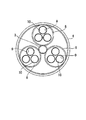
- FIG. 4 is a plan view for explaining the method of polishing the wafer substrate 10 and the layout of the holes 9 in the carrier 8 in this example.
- each carrier 8 in this example has their centers C9 located on a circumference P that is concentric with the carrier 8, and rotate with respect to the center P of the circle P (the center of the carrier 8) CP. They are arranged at equal intervals on the circle P so as to be point-symmetric.
- the size of the hole 9 is such that the area ratio between the circle P passing through the center C9 of the hole 9 and the hole 9 substantially equal to the wafer substrate 10 is 1.33 or more and less than 2.0, more preferably, It is set to 1.33 or more and 1.5 or less. That is, the radius R of the circle P and the radius r of the hole 9 are [Formula 1] 1.33 ⁇ (R / r) 2 ⁇ 1.5 It is set to become.
- the lower limit of the specified range of this area ratio is 1.3333. . . It may be above, and may be 1.334 or more.
- the carrier 8 can be provided with only two holes 9, and the wafer processed with the same carrier 8 This is not preferable because the processing of the substrate 10 is not uniform, and the effect of preventing the sagging of the wafer substrate 10 is not achieved. Further, when the upper limit of the area ratio is set to 2 or more and the three holes 9 are provided in the carrier 8, the distance between the wafer substrates 10 becomes too long, which is effective in preventing the sagging of the wafer substrates 10. Since it does not play, it is not preferable.
- the upper limit of the area ratio is 2 or more and the carrier 8 is provided with four or more holes 9, the pressure concentration is not sufficiently dispersed, which is effective in preventing the sagging of the wafer substrate 10. Since it does not play, it is not preferable.
- the upper limit of the area ratio is more than 1.5 and less than 2, it is possible to prevent sagging, but in order to obtain sufficient flatness as a product wafer, it is more preferably 1.5 or less preferable.
- the wafer 10 and the hole 9 have substantially the same size.
- the diameter of the hole 9 is 201 mm
- the diameter of the hole 9 is 302 mm. Is done.
- the wafer 10 is double-side polished using the carrier 8 in which the holes 9 are formed as described above, so that the peripheral portion of the wafer 10 is prevented from sagging, and a polished wafer with high flatness is obtained. It can be manufactured.
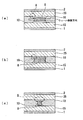
- FIG. 5 is a schematic cross-sectional view showing a polished state.
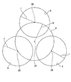
- the planar arrangement of the holes 9 in the carrier 8 is brought close to each other so that the arrangement of the wafer substrate 10 is concentrated on the center of the carrier 8 as shown in FIGS.
- the polishing pressure from the polishing cloths 15 and 25 is dispersed to the adjacent wafer substrate 10 that is close as indicated by reference numeral B in FIG.
- the polishing cloths 15 and 25 on the surface of the flexible surface plate are used as the wafer substrate. It will be in the state which deform
- the polishing cloth in the vicinity between the adjacent wafer substrates 10 is reduced by reducing the distance between the wafer substrates 10 (distance between the holes 9).
- the amount of deformation of 15 and 25 can be reduced.
- the pressure concentration in the peripheral portion of the wafer substrate 10 is reduced in the vicinity of the peripheral portion of the wafer substrate 10.
- the occurrence of sagging at the peripheral edge of the wafer substrate 10 can be reduced.
- a wafer substrate 10 with high flatness can be manufactured by avoiding a decrease or the like.
- the pressure from the polishing cloths 15 and 25 may be concentrated in the vicinity of the peripheral portion of the wafer substrate 10, and the peripheral sagging of the wafer substrate 10 may occur.
- the distance between the wafer substrates 10 to be polished on both sides is reduced to bring the wafer substrates 10 closer to each other, so that one carrier 8 is disposed in three holes 9.
- Each wafer substrate 10 can be brought close to a state of polishing as if it were a single wafer substrate 10.
- the length of pressure concentration is partially made with respect to the entire peripheral length of one wafer substrate 10, that is, the polishing cloths 15 and 25 on the surfaces of the flexible surface plates 1 and 2 are provided.
- the pressure from the polishing cloths 15 and 25 is concentrated on the peripheral portion of the wafer substrate 10, and the portion where the polishing state at the peripheral portion of the wafer substrate 10 becomes large is reduced. It becomes possible. As a result, it is possible to alleviate the concentration of polishing pressure on the entire circumference of the peripheral edge of one wafer substrate 10 at the end of polishing, and polishing each wafer substrate 10 while polishing to the extent that scratches and deposits on the back surface can be removed. It is possible to reduce the occurrence of sagging at the peripheral edge.
- the number of carriers 8 is three. However, other numbers may be used.
- the arrangement of the holes 9 or the wafer substrate 10 in each carrier 8 is the above-described configuration. If so, any configuration of the polishing apparatus can be applied.
- the polishing amount of the back surface of the silicon epitaxial wafer substrate is equal to or more than the polishing amount of the front surface.
- the polishing amount on the front surface of the wafer substrate is preferably in the range of 0.01 to 0.1 ⁇ m, and the polishing amount on the back surface is preferably in the range of 0.1 to 0.3 ⁇ m.
- the surface of the wafer substrate is mirror-polished.
- the polishing amount for mirror polishing is, for example, 0.01 to 0.2 ⁇ m.
- the flatness of the wafer substrate is ensured by the double-sided simultaneous polishing E performed before the epitaxial growth step G, as shown in FIG.
- the double-sided simultaneous polishing H1 performed after the epitaxial growth step G can maintain the haze level on the wafer surface without mirror polishing before the epitaxial growth step.
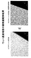
- the double-sided simultaneous polishing H1 after the epitaxial growth can remove the scratches with the susceptor of the epitaxial reactor and the deposit on the back surface (back surface deposit) generated on the back surface of the wafer as shown in FIG. It is possible to suppress the decrease in flatness and the generation of particles due to scratches and deposits.
- the double-sided simultaneous polishing H1 removes irregularities due to contact scratches or deposits on the back surface of the wafer and improves the flatness of the back surface, the amount of polishing of the epitaxial layer on the wafer surface becomes uniform in the surface, and the epitaxial layer The thickness becomes uniform.
- the polishing amount on the wafer surface is made as small as possible to remove the oxide film on the surface by double-sided simultaneous polishing H1 after epitaxial growth, the thickness of the epitaxial layer on the surface can be kept uniform.
- a p-type silicon single crystal ingot having a main axis orientation of ⁇ 100> and a diameter of 305 mm is manufactured by the Czochralski pulling method, and this ingot is ground to a diameter of 300 mm, then notched, and has a resistivity of 5 to 10 m ⁇ cm.
- a block was cut out. This block was sliced to a predetermined thickness using a wire saw to obtain a wafer substrate.
- the wafer substrate was sandwiched between upper and lower grinding surface plates of a double-sided grinding machine, and both the front and back surfaces of the wafer substrate were ground while supplying slurry containing abrasive grains (lapping step B shown in FIG. 1).
- the surface of the wafer substrate was ground using a grindstone containing diamond (single-side grinding step C in FIG. 1).
- Example 1 The wafer substrate ground as described above is sandwiched between upper and lower surface plates of a double-side polishing apparatus equipped with a hard polishing pad, and both surfaces of the wafer substrate are simultaneously polished by 12 ⁇ m under abrasive-free conditions (first double-sided in FIG. 1). Polishing step (rough polishing) E).
- the wafer substrate is set in the epitaxial reaction furnace, and before supplying the reaction gas, a halogenated gas is supplied into the reaction furnace to remove the oxide film formed on the surface of the wafer substrate. (Etching step F in FIG. 1). Subsequently, a reaction gas was supplied to form an epitaxial layer of about 3 ⁇ m on the surface of the wafer substrate (epitaxial growth step G in FIG. 1).
- the wafer substrate on which the epitaxial layer is formed is set in the hole 9 of the carrier 8 of the double-side polishing apparatus shown in FIG. 2, and the lower surface plate 1 is supplied while supplying the polishing liquid with a predetermined pressure applied to the wafer substrate.
- the upper surface plate 2, the sun gear 3, and the internal gear 4 were rotated in a predetermined direction at a predetermined speed (double-sided simultaneous polishing step H1 in FIG. 1).
- the polishing amount on the front surface of the wafer substrate was 0.05 ⁇ m
- the polishing amount on the back surface was 0.2 ⁇ m.
- the surface of the wafer substrate was mirror-polished (single-sided mirror-polishing step H2 in FIG. 1).
- the polishing amount of this mirror polishing was 0.1 ⁇ m.
- the partial site of flatness SFQR is a site that is missing because the wafer is circular in a state where the surface of one wafer is divided into, for example, 25 mm ⁇ 25 mm square sites or 26 mm ⁇ 8 mm rectangular sites. Site).
- the flatness shown in FIG. 8 is a value having about 50 partial sites as a population.
- the haze level of the epitaxial layer surface of the wafer substrate after the single-sided mirror polishing step H2 is determined using the DWO mode by using a product name inspection device (model: Surfscan SP2) with no pattern on the wafer manufactured by KLA-Tencor Corporation.
- a product name inspection device model: Surfscan SP2
- the haze level after the epitaxial growth step G was 0.3 ppm (corresponding to 39 nm as the minimum particle size capable of detecting SP2), which was confirmed to be a good haze level.
- FIG. 8 shows the results of measuring the flatness (SFQR partial site) after the mirror polishing process before the epitaxial growth process, after the epitaxial growth process, and after the mirror polishing process after the epitaxial growth process.
Landscapes
- Mechanical Treatment Of Semiconductor (AREA)
- Finish Polishing, Edge Sharpening, And Grinding By Specific Grinding Devices (AREA)
Abstract
Description
[式1]1.33≦(R/r)2 ≦1.5
となるように設定されている。
チョクラルスキー引上げ法により、主軸方位が<100>で、直径305mmのp型シリコン単結晶インゴットを製造し、このインゴットを直径300mmに外周研削したのち、ノッチ加工し、抵抗率が5~10mΩcmのブロックを切り出した。このブロックを、ワイヤーソーを用いて所定厚さにスライスしウェーハ基板を得た。
上記のようにして研削されたウェーハ基板を、硬質研磨パッドが装着された両面研磨装置の上下定盤で挟み、無砥粒条件でウェーハ基板の両面を同時に12μm研磨した(図1の第1両面研磨工程(粗研磨)E)。
上記実施例1に対し、図1の第1両面研磨工程(粗研磨)Eの後に、ウェーハ基板の表面を鏡面研磨し、また図1の両面同時研磨工程H1を省略した工程でウェーハ基板を作製した。これ以外の条件は上記実施例1と同じ条件とした。
図8の結果から、実施例1の工程で得られたウェーハ基板のパーシャルサイト平坦度は、比較例1の従来技術の工程で得られたウェーハ基板の平坦度に比べ、極めて良好であることが確認された。
2…上定盤
3…太陽歯車
4…内歯歯車
8…キャリア
9…ホール
10…シリコンウェーハ基板
Claims (10)
- シリコン単結晶基板にエピタキシャル層を成長させる成長工程と、
前記成長工程の前に、前記シリコン単結晶基板の両主面を同時に粗研磨する第1研磨工程と、
前記成長工程の後に、前記シリコン単結晶基板の両主面を同時に仕上げ研磨する第2研磨工程と、を有することを特徴とするシリコンエピタキシャルウェーハの製造方法。 - 請求項1に記載のシリコンエピタキシャルウェーハの製造方法において、
前記第2研磨工程は、前記シリコン単結晶基板の両主面を研磨する第1工程と、前記シリコン単結晶基板の表面を鏡面研磨する第2工程とを有することを特徴とするシリコンエピタキシャルウェーハの製造方法。 - 請求項1又は2に記載のシリコンエピタキシャルウェーハの製造方法において、
前記第1研磨工程は無砥粒の条件で粗研磨することを特徴とするシリコンエピタキシャルウェーハの製造方法。 - 請求項2又は3に記載のシリコンエピタキシャルウェーハの製造方法において、
前記第1工程は、複数のシリコン単結晶基板を研磨装置のキャリアに対し、当該キャリアにおける前記シリコン単結晶基板の保持位置が、前記複数のシリコン単結晶基板の中心が同一の円周上になり、且つ当該複数のシリコン単結晶基板の中心を通る円と単一の前記シリコン単結晶基板との面積比が1.33以上、2.0未満となるように保持し、上下の回転定盤間で前記キャリアを回転させることにより、研磨を行う工程であることを特徴とするシリコンエピタキシャルウェーハの製造方法。 - 請求項4に記載のシリコンエピタキシャルウェーハの製造方法において、
前記キャリアは、3枚のシリコン単結晶基板を保持することを特徴とするシリコンエピタキシャルウェーハの製造方法。 - 請求項1~5のいずれか一項に記載のシリコンエピタキシャルウェーハの製造方法において、
前記成長工程は、前記エピタキシャル層を成長させる前にハロゲン化ガスにより前記シリコン単結晶基板の表面をエッチングするエッチング工程を含むことを特徴とするシリコンエピタキシャルウェーハの製造方法。 - 請求項1~5のいずれか一項に記載のシリコンエピタキシャルウェーハの製造方法において、
前記第1両面研磨工程と前記成長工程との間に、前記シリコン単結晶基板の表面を湿式エッチング処理するエッチング工程を有することを特徴とするシリコンエピタキシャルウェーハの製造方法。 - 請求項1~7のいずれか一項に記載のシリコンエピタキシャルウェーハの製造方法において、
前記第2両面研磨工程は、前記シリコン単結晶基板の裏面の研磨量が表面の研磨量以上であることを特徴とするシリコンエピタキシャルウェーハの製造方法。 - 請求項8に記載のシリコンエピタキシャルウェーハの製造方法において、
前記裏面の研磨量が0.1μm以上であることを特徴とするシリコンエピタキシャルウェーハの製造方法。 - 請求項8又は9に記載のシリコンエピタキシャルウェーハの製造方法において、
前記表面の研磨量が0.1μm以下であることを特徴とするシリコンエピタキシャルウェーハの製造方法。
Priority Applications (3)
| Application Number | Priority Date | Filing Date | Title |
|---|---|---|---|
| DE112010002274.7T DE112010002274B4 (de) | 2009-05-08 | 2010-05-07 | Verfahren zur Herstellung eines Siliziumepitaxialwafers |
| KR1020117027817A KR101328775B1 (ko) | 2009-05-08 | 2010-05-07 | 실리콘 에피택셜 웨이퍼의 제조 방법 |
| US13/318,950 US8999061B2 (en) | 2009-05-08 | 2010-05-07 | Method for producing silicon epitaxial wafer |
Applications Claiming Priority (2)
| Application Number | Priority Date | Filing Date | Title |
|---|---|---|---|
| JP2009113157A JP5381304B2 (ja) | 2009-05-08 | 2009-05-08 | シリコンエピタキシャルウェーハの製造方法 |
| JP2009-113157 | 2009-05-08 |
Publications (1)
| Publication Number | Publication Date |
|---|---|
| WO2010128671A1 true WO2010128671A1 (ja) | 2010-11-11 |
Family
ID=43050168
Family Applications (1)
| Application Number | Title | Priority Date | Filing Date |
|---|---|---|---|
| PCT/JP2010/057795 Ceased WO2010128671A1 (ja) | 2009-05-08 | 2010-05-07 | シリコンエピタキシャルウェーハの製造方法 |
Country Status (5)
| Country | Link |
|---|---|
| US (1) | US8999061B2 (ja) |
| JP (1) | JP5381304B2 (ja) |
| KR (1) | KR101328775B1 (ja) |
| DE (1) | DE112010002274B4 (ja) |
| WO (1) | WO2010128671A1 (ja) |
Cited By (1)
| Publication number | Priority date | Publication date | Assignee | Title |
|---|---|---|---|---|
| WO2022215370A1 (ja) * | 2021-04-07 | 2022-10-13 | 信越半導体株式会社 | ウェーハの加工方法及びウェーハ |
Families Citing this family (4)
| Publication number | Priority date | Publication date | Assignee | Title |
|---|---|---|---|---|
| JP5750877B2 (ja) * | 2010-12-09 | 2015-07-22 | 株式会社Sumco | ウェーハの片面研磨方法、ウェーハの製造方法およびウェーハの片面研磨装置 |
| JP5799935B2 (ja) * | 2012-11-13 | 2015-10-28 | 株式会社Sumco | 半導体エピタキシャルウェーハの製造方法、半導体エピタキシャルウェーハ、および固体撮像素子の製造方法 |
| JP6146213B2 (ja) | 2013-08-30 | 2017-06-14 | 株式会社Sumco | ワークの両面研磨装置及び両面研磨方法 |
| CN114361028A (zh) * | 2021-03-18 | 2022-04-15 | 青岛惠科微电子有限公司 | 一种芯片及其制作方法 |
Citations (6)
| Publication number | Priority date | Publication date | Assignee | Title |
|---|---|---|---|---|
| JP2000243699A (ja) * | 1999-02-23 | 2000-09-08 | Hitachi Ltd | 半導体ウェハの製造方法および半導体装置の製造方法 |
| JP2003077870A (ja) * | 2001-07-05 | 2003-03-14 | Wacker Siltronic Ag | 半導体ウェーハを同時に両面で材料除去加工するための方法 |
| JP2005209862A (ja) * | 2004-01-22 | 2005-08-04 | Komatsu Electronic Metals Co Ltd | 半導体エピタキシャルウェーハの製造方法 |
| JP2006054428A (ja) * | 2004-06-11 | 2006-02-23 | Soi Tec Silicon On Insulator Technologies | ウェーハの製造方法 |
| JP2007214368A (ja) * | 2006-02-09 | 2007-08-23 | Hitachi Cable Ltd | Movpe用化合物半導体ウェハ、その製造方法及びmovpe用化合物半導体エピタキシャルウェハの製造方法 |
| JP2008088051A (ja) * | 2006-09-06 | 2008-04-17 | Sumco Corp | エピタキシャルウェーハおよびその製造方法 |
Family Cites Families (11)
| Publication number | Priority date | Publication date | Assignee | Title |
|---|---|---|---|---|
| US3436259A (en) | 1966-05-12 | 1969-04-01 | Ibm | Method for plating and polishing a silicon planar surface |
| JPH0817163A (ja) | 1994-06-29 | 1996-01-19 | Sony Corp | ディスクカートリッジ |
| MY133700A (en) * | 1996-05-15 | 2007-11-30 | Kobe Steel Ltd | Polishing fluid composition and polishing method |
| DE19704546A1 (de) | 1997-02-06 | 1998-08-13 | Wacker Siltronic Halbleitermat | Verfahren zur Herstellung einer einseitig beschichteten und mit einem Finish versehenen Halbleiterscheibe |
| US6881644B2 (en) * | 1999-04-21 | 2005-04-19 | Silicon Genesis Corporation | Smoothing method for cleaved films made using a release layer |
| DE10196115B4 (de) | 2000-04-24 | 2011-06-16 | Sumitomo Mitsubishi Silicon Corp. | Verfahren zum Polieren eines Halbleiterwafers |
| US6709981B2 (en) * | 2000-08-16 | 2004-03-23 | Memc Electronic Materials, Inc. | Method and apparatus for processing a semiconductor wafer using novel final polishing method |
| JP3991598B2 (ja) | 2001-02-26 | 2007-10-17 | 株式会社Sumco | ウエーハ研磨方法 |
| US6849548B2 (en) * | 2002-04-05 | 2005-02-01 | Seh America, Inc. | Method of reducing particulate contamination during polishing of a wafer |
| JP4854936B2 (ja) * | 2004-06-15 | 2012-01-18 | 信越半導体株式会社 | シリコンウエーハの製造方法及びシリコンウエーハ |
| JP4370990B2 (ja) * | 2004-07-12 | 2009-11-25 | エプソントヨコム株式会社 | 圧電発振器及びその製造方法 |
-
2009
- 2009-05-08 JP JP2009113157A patent/JP5381304B2/ja active Active
-
2010
- 2010-05-07 WO PCT/JP2010/057795 patent/WO2010128671A1/ja not_active Ceased
- 2010-05-07 KR KR1020117027817A patent/KR101328775B1/ko active Active
- 2010-05-07 US US13/318,950 patent/US8999061B2/en active Active
- 2010-05-07 DE DE112010002274.7T patent/DE112010002274B4/de active Active
Patent Citations (6)
| Publication number | Priority date | Publication date | Assignee | Title |
|---|---|---|---|---|
| JP2000243699A (ja) * | 1999-02-23 | 2000-09-08 | Hitachi Ltd | 半導体ウェハの製造方法および半導体装置の製造方法 |
| JP2003077870A (ja) * | 2001-07-05 | 2003-03-14 | Wacker Siltronic Ag | 半導体ウェーハを同時に両面で材料除去加工するための方法 |
| JP2005209862A (ja) * | 2004-01-22 | 2005-08-04 | Komatsu Electronic Metals Co Ltd | 半導体エピタキシャルウェーハの製造方法 |
| JP2006054428A (ja) * | 2004-06-11 | 2006-02-23 | Soi Tec Silicon On Insulator Technologies | ウェーハの製造方法 |
| JP2007214368A (ja) * | 2006-02-09 | 2007-08-23 | Hitachi Cable Ltd | Movpe用化合物半導体ウェハ、その製造方法及びmovpe用化合物半導体エピタキシャルウェハの製造方法 |
| JP2008088051A (ja) * | 2006-09-06 | 2008-04-17 | Sumco Corp | エピタキシャルウェーハおよびその製造方法 |
Cited By (3)
| Publication number | Priority date | Publication date | Assignee | Title |
|---|---|---|---|---|
| WO2022215370A1 (ja) * | 2021-04-07 | 2022-10-13 | 信越半導体株式会社 | ウェーハの加工方法及びウェーハ |
| JP2022160934A (ja) * | 2021-04-07 | 2022-10-20 | 信越半導体株式会社 | ウェーハの加工方法及びウェーハ |
| JP7676893B2 (ja) | 2021-04-07 | 2025-05-15 | 信越半導体株式会社 | ウェーハの加工方法及びウェーハ |
Also Published As
| Publication number | Publication date |
|---|---|
| US20120090536A1 (en) | 2012-04-19 |
| DE112010002274T5 (de) | 2012-10-04 |
| KR20120011053A (ko) | 2012-02-06 |
| DE112010002274B4 (de) | 2020-02-13 |
| KR101328775B1 (ko) | 2013-11-13 |
| JP2010263095A (ja) | 2010-11-18 |
| JP5381304B2 (ja) | 2014-01-08 |
| US8999061B2 (en) | 2015-04-07 |
Similar Documents
| Publication | Publication Date | Title |
|---|---|---|
| US9396945B2 (en) | Method for producing SiC substrate | |
| JP5644401B2 (ja) | エピタキシャルウェーハの製造方法およびエピタキシャルウェーハ | |
| JP3169120B2 (ja) | 半導体鏡面ウェーハの製造方法 | |
| KR101994782B1 (ko) | 경면연마 웨이퍼의 제조방법 | |
| JP5479390B2 (ja) | シリコンウェーハの製造方法 | |
| WO2013187441A1 (ja) | 半導体ウェーハの製造方法 | |
| TW201351494A (zh) | 晶圓的雙面研磨方法 | |
| JP5381304B2 (ja) | シリコンエピタキシャルウェーハの製造方法 | |
| KR101390307B1 (ko) | 에피택셜 실리콘 웨이퍼의 제조방법 | |
| JP2012043892A (ja) | シリコンエピタキシャルウェーハの製造方法およびシリコンエピタキシャルウェーハ | |
| KR102165589B1 (ko) | 실리콘 웨이퍼 연마 방법, 실리콘 웨이퍼 제조 방법 및 실리콘 웨이퍼 | |
| WO2016170721A1 (ja) | エピタキシャルウェーハの製造方法 | |
| TWI872474B (zh) | 兩面研磨用載具及使用此之矽晶圓的兩面研磨方法及裝置 | |
| JP5287982B2 (ja) | シリコンエピタキシャルウェーハの製造方法 | |
| JP5282440B2 (ja) | 評価用ウェーハ及び両面研磨の研磨代の評価方法 | |
| JP2011091143A (ja) | シリコンエピタキシャルウェーハの製造方法 | |
| JP2017117915A (ja) | シリコンウェーハの面取り方法、シリコンウェーハの製造方法およびシリコンウェーハ | |
| JP2009135180A (ja) | 半導体ウェーハの製造方法 |
Legal Events
| Date | Code | Title | Description |
|---|---|---|---|
| 121 | Ep: the epo has been informed by wipo that ep was designated in this application |
Ref document number: 10772188 Country of ref document: EP Kind code of ref document: A1 |
|
| WWE | Wipo information: entry into national phase |
Ref document number: 1120100022747 Country of ref document: DE Ref document number: 112010002274 Country of ref document: DE |
|
| ENP | Entry into the national phase |
Ref document number: 20117027817 Country of ref document: KR Kind code of ref document: A |
|
| WWE | Wipo information: entry into national phase |
Ref document number: 13318950 Country of ref document: US |
|
| 122 | Ep: pct application non-entry in european phase |
Ref document number: 10772188 Country of ref document: EP Kind code of ref document: A1 |