WO2010128615A1 - 記憶素子及び記憶方法 - Google Patents
記憶素子及び記憶方法 Download PDFInfo
- Publication number
- WO2010128615A1 WO2010128615A1 PCT/JP2010/056650 JP2010056650W WO2010128615A1 WO 2010128615 A1 WO2010128615 A1 WO 2010128615A1 JP 2010056650 W JP2010056650 W JP 2010056650W WO 2010128615 A1 WO2010128615 A1 WO 2010128615A1
- Authority
- WO
- WIPO (PCT)
- Prior art keywords
- layer
- value
- free layer
- magnetization
- free
- Prior art date
- Legal status (The legal status is an assumption and is not a legal conclusion. Google has not performed a legal analysis and makes no representation as to the accuracy of the status listed.)
- Ceased
Links
Images



Classifications
-
- G—PHYSICS
- G01—MEASURING; TESTING
- G01R—MEASURING ELECTRIC VARIABLES; MEASURING MAGNETIC VARIABLES
- G01R33/00—Arrangements or instruments for measuring magnetic variables
- G01R33/02—Measuring direction or magnitude of magnetic fields or magnetic flux
- G01R33/06—Measuring direction or magnitude of magnetic fields or magnetic flux using galvano-magnetic devices
- G01R33/09—Magnetoresistive devices
- G01R33/093—Magnetoresistive devices using multilayer structures, e.g. giant magnetoresistance sensors
-
- B—PERFORMING OPERATIONS; TRANSPORTING
- B82—NANOTECHNOLOGY
- B82Y—SPECIFIC USES OR APPLICATIONS OF NANOSTRUCTURES; MEASUREMENT OR ANALYSIS OF NANOSTRUCTURES; MANUFACTURE OR TREATMENT OF NANOSTRUCTURES
- B82Y25/00—Nanomagnetism, e.g. magnetoimpedance, anisotropic magnetoresistance, giant magnetoresistance or tunneling magnetoresistance
-
- G—PHYSICS
- G11—INFORMATION STORAGE
- G11C—STATIC STORES
- G11C11/00—Digital stores characterised by the use of particular electric or magnetic storage elements; Storage elements therefor
- G11C11/02—Digital stores characterised by the use of particular electric or magnetic storage elements; Storage elements therefor using magnetic elements
- G11C11/16—Digital stores characterised by the use of particular electric or magnetic storage elements; Storage elements therefor using magnetic elements using elements in which the storage effect is based on magnetic spin effect
-
- G—PHYSICS
- G11—INFORMATION STORAGE
- G11C—STATIC STORES
- G11C11/00—Digital stores characterised by the use of particular electric or magnetic storage elements; Storage elements therefor
- G11C11/02—Digital stores characterised by the use of particular electric or magnetic storage elements; Storage elements therefor using magnetic elements
- G11C11/16—Digital stores characterised by the use of particular electric or magnetic storage elements; Storage elements therefor using magnetic elements using elements in which the storage effect is based on magnetic spin effect
- G11C11/161—Digital stores characterised by the use of particular electric or magnetic storage elements; Storage elements therefor using magnetic elements using elements in which the storage effect is based on magnetic spin effect details concerning the memory cell structure, e.g. the layers of the ferromagnetic memory cell
-
- H—ELECTRICITY
- H10—SEMICONDUCTOR DEVICES; ELECTRIC SOLID-STATE DEVICES NOT OTHERWISE PROVIDED FOR
- H10N—ELECTRIC SOLID-STATE DEVICES NOT OTHERWISE PROVIDED FOR
- H10N50/00—Galvanomagnetic devices
- H10N50/10—Magnetoresistive devices
Definitions
- the present invention relates to a storage element and a storage method.
- a memory element using a magnetic multilayer film that exhibits a tunneling magnetoresistive (TMR) effect is applied to a nonvolatile memory such as an MRAM.
- the multilayer film of the tunnel magnetoresistive element has two magnetic layers and an insulating layer sandwiched therebetween.
- the insulating layer is made of a material such as alumina or MgO.
- the insulating layer is thin, and when a sense current is passed vertically on the multilayer film surface to operate as a memory element, each film is stacked through an insulating layer sandwiched between two magnetic layers by the tunnel effect. A tunnel current flows vertically.
- the resistance value of the tunnel magnetoresistive element is small when the magnetization directions of the two magnetic layers are the same, and large when they are opposite. In a conventionally used rectangular or elliptical tunnel magnetoresistive element, it is possible to fabricate a memory element adopting the binary method by making the resistance value large and small correspond to “0” and “1”.
- a ternary or quaternary memory element may be manufactured instead of a binary memory element.
- a multi-layered film in which three or more magnetic layers having different coercive forces are stacked and a plurality of magnetoresistive elements having different tunnel resistance values are connected in series can be considered. There is a problem that the cost is high.
- the present invention was created to solve the above-described disadvantages of the prior art, and an object of the present invention is to provide a storage element and a storage method for storing ternary or quaternary values with a conventional simple multilayer film structure. is there.
- the present invention is magnetized in a direction perpendicular to the film thickness direction and has a fixed layer having a predetermined coercive force, and is magnetized in a direction parallel to the magnetization direction of the fixed layer.
- the fixed layer has a free layer smaller than the fixed layer, and an insulating layer sandwiched between the fixed layer and the free layer.
- the magnetization of the fixed layer A storage element in which a first and a second magnetoresistive element in which a tunnel current flows in the insulating layer with a resistance value corresponding to a difference between a direction and a magnetization direction of the free layer, the first magnetoresistance
- the length of the free layer of the element along the magnetization direction is longer than the length of the second magnetoresistive element along the magnetization direction of the second magnetoresistive element, with respect to an external magnetic field opposite to the magnetization direction.
- the coercivity of the free layer of the second magnetoresistive element is the first magnetism.
- resistive element is greater than the coercive force of the free layer, ternary or 4 values by the magnitude of the resistance value of the memory element to be stored.
- a fixed layer magnetized in a direction perpendicular to the film thickness direction and having a predetermined coercive force, and magnetized in a direction parallel to the magnetization direction of the fixed layer, the coercive force is smaller than that of the fixed layer.
- the free layer is formed in a shape having a planar shape having a width and a longitudinal direction longer than the width, and the longitudinal directions of the free layers of the first and second magnetoresistive elements are arranged at right angles to each other.
- the free layer of the first magnetoresistive element is the free layer Magnetized parallel to the longitudinal direction
- the free layer of the second magnetoresistive element is magnetized parallel to the length direction of the width of the free layer, and an external magnetic field opposite to the magnetization direction is applied.
- the coercive force of the free layer of the second magnetoresistive element is made larger than the coercive force of the free layer of the first magnetoresistive element, and a ternary value or a quaternary value is stored as the resistance value. Storage element.
- a fixed layer magnetized in a direction perpendicular to the film thickness direction and having a predetermined coercive force, and magnetized in a direction parallel to the magnetization direction of the fixed layer, the coercive force is smaller than that of the fixed layer.
- the length along the magnetization direction is longer than the length along the magnetization direction of the free layer of the second magnetoresistive element, and the second magnetic field is applied to a spin injection current that reverses the magnetization direction.
- the strength of the first magnetoresistive element is greater than the strength against magnetization reversal when the spin injection current of the free layer flows, and the memory stores 3 or 4 values as the resistance value. It is an element.
- a fixed layer magnetized in a direction perpendicular to the film thickness direction and having a predetermined coercive force, and magnetized in a direction parallel to the magnetization direction of the fixed layer, the coercive force is smaller than that of the fixed layer.
- the free layer is formed in a shape having a planar shape having a width and a longitudinal direction longer than the width, and the longitudinal directions of the free layers of the first and second magnetoresistive elements are arranged at right angles to each other.
- the free layer of the first magnetoresistive element is the free layer A spin injection current that is magnetized parallel to the longitudinal direction
- the free layer of the second magnetoresistive element is magnetized parallel to the length direction of the width of the free layer to reverse the magnetization direction
- the strength against magnetization reversal when the spin injection current of the free layer of the second magnetoresistive element flows is that when the spin injection current of the free layer of the first magnetoresistive element flows.
- This is a storage element that is larger than the strength against magnetization reversal and stores three or four values in terms of the resistance value.
- the present invention is a memory element, wherein the free layers of the first and second magnetoresistive elements are connected to each other.
- the present invention is a memory element, wherein the fixed layers of the first and second magnetoresistive elements are connected to each other.
- the present invention is a memory element, wherein the insulating layers of the first and second magnetoresistive elements are connected to each other.
- the present invention is a storage method for storing first, second, and third values using the storage element, wherein the first and second magnetoresistors are used for storing the first value.
- the first and second magnetoresistive elements are oriented in the same direction as the magnetization direction of the fixed layer, so that both elements exhibit the same magnetization direction resistance value. In order to store the parallel resistance value of the second magnetoresistive element in correspondence with the first value, and to store the second value, both the first and second magnetoresistive elements have opposite magnetization directions.
- the magnetization direction of the free layer of the first and second magnetoresistive elements is directed to the opposite direction to the magnetization direction of the fixed layer, respectively.
- the magnetization direction of the free layer of the one magnetoresistive element is oriented in the same direction as the magnetization direction of the fixed layer so that the magnetoresistive element exhibits the same magnetization direction resistance value, and the other magnetoresistive element
- the parallel resistance of the first and second magnetoresistive elements is set so that the magnetization direction of the free layer of the other magnetoresistive element is directed to the opposite direction to the magnetization direction of the fixed layer so as to indicate a magnetization unidirectional resistance value.
- a storage method for storing a value in association with the third value is a storage method for rewriting a first value, a second value, and a third value, and storing the rewritten value, wherein only the magnetization direction of the free layer of the first magnetoresistive element is reversed.
- an external magnetic field larger than the coercive force of the free layer of the first magnetoresistive element and smaller than the coercive force of the free layer of the second magnetoresistive element is applied to the first magnetoresistive element.
- the storage method stores the rewritten value by applying in the direction opposite to the magnetization direction of the free layer.
- the present invention is a storage method for rewriting a first value, a second value, and a third value, and storing the rewritten value, wherein only the magnetization direction of the free layer of the first magnetoresistive element is reversed.
- the magnetization direction of the free layer of the first magnetoresistive element is reversed, and the strength of the first magnetoresistive element against the magnetization reversal when the spin injection current of the free layer flows is greater than
- the storage method stores a rewritten value by supplying a spin injection current smaller than the strength against magnetization reversal when the spin injection current of the free layer of the second magnetoresistive element flows.
- the present invention is a storage method for measuring a resistance value of the storage element and reading a value stored from the resistance value, measuring the resistance value of the storage element and comparing it with a reference value, and The case where it is determined that the resistance value of the resistance element is the magnetization direction resistance value is the first value, and the case where it is determined that the resistance value of both the magnetoresistance elements is the magnetization direction resistance value
- the magnetization direction of the magnetic layer when the magnetization direction of the magnetic layer is parallel to the direction of the external magnetic field and the major axis is longer than the minor axis (here, 1.5 times or longer), the magnetization direction is parallel to the major axis.
- the layer pays attention to the fact that the magnetization direction can be reversed with an external magnetic field smaller than that of the magnetic layer whose magnetization direction is parallel to the minor axis (referred to as magnetic shape anisotropy).
- the state in which the magnetic layer is magnetized is a state in which the N pole and the S pole appear at both ends of the magnetization direction of the magnetic layer. Create a magnetic field (demagnetizing field) in the opposite direction.
- the size of the internal demagnetizing field is proportional to the size of the magnetization, and at the same time, depends on the shape of the magnetization direction. Magnetic field becomes 0).
- the magnetic field acting inside the magnetic layer is considered to be given by the difference between the external magnetic field and the demagnetizing field.
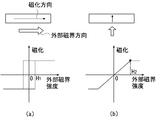
- FIG. 3 (a) and 3 (b) show the strength and magnetism of an external magnetic field when an external magnetic field parallel to and opposite to the magnetization direction is applied to a magnetic layer magnetized in a direction parallel to the major axis and minor axis. It is the result of having measured the relationship of the magnetization of the layer.
- the magnetic layer magnetized in the direction parallel to the long axis is inverted by a weak external magnetic field ⁇ H 1 to saturate the magnetization (FIG. 3A), but the magnetic layer magnetized in the direction parallel to the short axis is Since the magnetization changes linearly until it is inverted at ⁇ H 2 larger than ⁇ H 1 , the magnetization is not saturated unless a large external magnetic field is applied (FIG. 3B).
- the present invention controls the area ratio of the free layers of the first and second magnetoresistive elements so that the magnetization directions of the free layer and the fixed layer of one magnetoresistive element are the same and the other magnetoresistive is The resistance value when the magnetization directions of the free layer and the fixed layer of the element are opposite directions, the resistance value when the magnetization directions of the free layer and the fixed layer of both magnetoresistive elements are the same direction, and the resistance value of both magnetoresistive elements
- This is a memory element that can control the resistance value when the magnetization directions of the free layer and the fixed layer are opposite to each other.
- the resistance value is not the maximum or minimum value, but the magnetic fields of the two magnetic layers of one element are in the same direction.
- An intermediate value can be taken when the magnetic fields of the two magnetic layers of the other element are in opposite directions, and a ternary or quaternary storage element can be obtained by discriminating the maximum value, intermediate value, and minimum value. .
- the storage capacity can be increased as compared with the binary storage medium without increasing the density of the storage elements.
- a multilayer film conventionally used can be used, there is no need to newly create a multilayer film having a complicated laminated structure, and a ternary or quaternary memory element can be obtained at low cost.
- FIG. 1 The top view of the memory element of this invention Sectional view taken along the line AA of the memory element of the present invention.
- Reference numeral 10 in FIG. 1 is a plan view of a memory element according to the present invention.
- the memory element 10 has first and second magnetoresistive elements 11 and 12.
- FIG. 2 is a cross-sectional view of the memory element 10 taken along the line AA.
- the first and second magnetoresistive elements 11 and 12 are magnetized in a direction parallel to the magnetization direction of the fixed layer 48 having a predetermined coercive force, the insulating layer 43, and the fixed layer 48, and the coercive force has a fixed layer 48. It has smaller free layers 22, 32.
- First and second magnetoresistive elements 11 and 12 are formed. After the free layers 22 and 32 are etched, a SiO 2 layer 41 is laminated from the free layers 22 and 32 side, and then the SiO 2 layer 41 is etched to expose the surfaces of the free layers 22 and 32.
- the second electrode 62 is formed so as to be in close contact with the surfaces of the free layers 22 and 32.
- the insulating layer 43 is thin, and when a voltage is applied between the free layers 22 and 32 and the fixed layer 48, a tunnel current flows in a direction perpendicular to each layer due to the tunnel effect.
- the conductance values of the first and second magnetoresistive elements 11 and 12 are large when the magnetization directions of the free layers 22 and 32 are the same as the magnetization direction of the fixed layer 48, and vice versa. Small in the direction (conductance value is the reciprocal of the resistance value). Accordingly, the first and second magnetoresistive elements 11 and 12 function as tunnel magnetoresistive elements.
- the planar shapes of the free layers 22 and 32 (hereinafter referred to as the first and second free layers) of the first and second magnetoresistive elements 11 and 12 are as follows. It has a width direction 52, 54 that is vertical and shorter than the length in the longitudinal direction.
- the length of the first free layer 22 in the longitudinal direction 51 is 1.5 times or more the length of the width direction 52.
- the first and second free layers 22 and 32 are magnetized in directions parallel to each other.
- the length along the magnetization direction of the first free layer 22 is longer than the length along the magnetization direction of the second free layer 32, where the first and second free layers 22, 32 are longitudinal.
- the directions 51 and 53 are arranged so as to be perpendicular to each other.
- the coercive force (hereinafter referred to as the first coercive force) of the first free layer 22 magnetized in the longitudinal direction 51 against the external magnetic field opposite to the magnetization direction is the first magnetized in the width direction 54. It is smaller than the coercive force of the second free layer 32 (hereinafter referred to as the second coercive force).
- the strength against magnetization reversal when the spin injection current of the first free layer 22 magnetized in the longitudinal direction 51 flows against the spin injection current that reverses the magnetization direction is magnetized in the width direction 54.
- the second free layer 32 is made smaller than the strength against magnetization reversal when the spin injection current flows.
- first and second free layers 22 and 32 are arranged so that the longitudinal directions 51 and 53 are perpendicular to each other.
- the present invention is not limited to this, and the first and second free layers 22 and 32 are arranged.
- the layers 22 and 32 are included in the present invention when the straight lines extending along the longitudinal directions 51 and 53 are arranged so as to intersect each other.
- the fixed layer 48 is in contact with and electrically connected to the first electrode 61, and the first and second free layers 22 and 32 are respectively connected to the second electrode 62. Is in contact with and electrically connected. Therefore, the memory element 10 forms a parallel connection circuit in which the first and second magnetoresistive elements 11 and 12 are connected in parallel.
- the minimum conductance values of the first and second magnetoresistive elements 11 and 12 are C1 and C2, respectively, and the maximum values are C1 + ⁇ C1 and C2 + ⁇ C2, respectively.
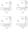
- FIG. 4A to 4D show changes in the magnetization directions F 1 and F 2 of the first and second free layers 22 and 32 with respect to the magnetization direction F 0 of the fixed layer 48 inside the memory element 10. ing.
- the conductance value is a maximum value close to the value represented by C1 + C2 + ⁇ C1 + ⁇ C2. (Because the current that originally flows through the low conductance portion flows into the high conductance portion, the change in the conductance of the entire element is not accurately ⁇ C1 + ⁇ C2, Close to that).
- the conductance of the memory element 10 has four conductance values of the maximum value C1 + C2 + ⁇ C1 + ⁇ C2, the first intermediate value C1 + C2 + ⁇ C1, the second intermediate value C1 + C2 + ⁇ C2, and the minimum value C1 + C2.
- the first conductance difference ⁇ C1 is larger than the second conductance difference ⁇ C2 ( ⁇ C1> ⁇ C2)
- the first intermediate value becomes a large intermediate value
- the second intermediate value becomes a small intermediate value.
- the second conductance difference ⁇ C2 ⁇ C1 ⁇ C2
- the second intermediate value becomes a large intermediate value
- the first intermediate value becomes a small intermediate value.
- the first reference value is placed between the maximum value and the large intermediate value
- the second reference value is placed between the small intermediate value and the minimum value
- the three conductances of maximum value, minimum value, and intermediate value are set.
- a ternary memory element can be obtained.
- a third reference value is placed between the large intermediate value and the small intermediate value, and the maximum value, the large intermediate value, the small intermediate value, and the minimum value are set.
- a four-value memory element is obtained by discriminating the four conductance values.
- FIG. 5 is a cross-sectional view showing an example of the storage device 1 such as an MRAM.
- the storage device 1 has a plurality of first and second wirings 5 and 6.
- the first wiring 5 is arranged parallel to each other with a predetermined interval, and the second wiring 6 intersects the first wiring 5 in a plane parallel to the plane where the first wiring 5 is arranged.
- the first and second wirings 5 and 6 are embedded in an insulating layer 2 such as SiO 2 .
- the memory element 10 of the present invention is disposed in the vicinity of the three-dimensional intersection position of the first and second wirings 5 and 6. Since the intersection positions of the first and second wirings 5 and 6 are arranged in a matrix, the memory elements 10 are arranged in a matrix.
- the first and second electrodes 61 and 62 of the memory element 10 are respectively connected to first and second wirings 5 and 6 that intersect in the vicinity of the memory element 10.
- the first and second wirings 5 and 6 are connected to the control device 8.
- the control device 8 selects the first and second wirings 5 and 6 to pass a current through the desired storage element 10, and the measurement device 9 stores the current flowing through the storage device 10.
- the conductance value is measured from the voltage and current between the electrodes of the element 10, and the measurement result is transmitted to the control device 8.
- the conductance value of the memory element 10 of the present invention can be obtained in three ways of the maximum value, the minimum value, and the intermediate value, and at least the maximum value and the minimum value of the conductance are set as the reference values in the control device 8. ing.
- the control device 8 compares the measurement result of the measurement device 9 with the set conductance value (reference value), and the measurement result corresponds to the maximum value, the minimum value, or between the maximum value and the minimum value (intermediate value). Judge whether to do.
- the control device 8 associates the determined result with information such as “0”, “1”, “2”, etc., and reads it as information. Therefore, in the storage device 1, the first and second wirings 5 and 6, the control device 8, and the measurement device 9 constitute a reading unit that reads information.
- the rewrite wiring 4 is extended along the wiring of the first wiring 5. Since the first wiring 5 intersects with the second wiring 6, the rewrite wiring 4 also intersects with the second wiring 6. Each memory element 10 is disposed between the rewrite wiring 4 and the second wiring 6 at the intersection of the rewrite wiring 4 and the second wiring 6. The rewrite wiring 4 is not in contact with the memory element 10 and the first and second wirings 5 and 6 and is insulated.
- the rewrite wiring 4 is connected to the control device 8.
- the positional relationship between the rewrite wiring 4 and the second wiring 6 and the memory element 10 is set in the control device 8.
- the control device 8 selects one of the target storage elements 10 among the rewrite wirings 4 and the second wirings 6 arranged in a lattice shape and energizes them.
- a magnetic field is generated around the rewrite wiring 4 and the second wiring 6, a composite magnetic field is generated near the intersection of the rewriting wiring 4 and the second wiring 6, and other elements are affected by the magnetic field. Absent. Therefore, only the memory elements 10 at the intersection of the selected wirings 4 and 6 among the plurality of memory elements 10 arranged in a matrix are exposed to the synthesized magnetic field.
- the energization conditions such as the direction and strength of the current flowing through the rewrite wiring 4 and the second wiring 6 are changed, the direction and strength of the synthetic magnetic field change.
- the energization conditions for creating each combined magnetic field that sets the conductance of the storage element 10 to the maximum value, the minimum value, and the intermediate value are obtained in advance and set in the control device 8.
- the control device 8 associates the information to be stored with the conductance of the storage element 10, and allows current to flow through the rewrite wiring 4 and the second wiring 6 under the energization condition that sets the conductance to an associated value, and stores desired storage information in the storage element 10. Memorize as conductance.
- the second wiring 6, the rewriting wiring 4, and the control device 8 serve as a rewriting means for rewriting information, but the rewriting means is not limited to this.
- the rewriting means may be composed of only the rewrite wiring 4 and the control device 8.
- the control device 8 selects the rewrite wiring 4 and energizes it, and rewrites the information in the storage element 10 on the selected rewrite wiring 4.
- the rewriting means may be constituted by the first and second wirings 5 and 6 and the control device 8 without providing the rewriting wiring 4.
- the control device 8 selects and energizes the first and second wirings 5 and 6, generates a synthetic magnetic field at the crossing position of the selected first and second wirings 5 and 6, and Information in the memory element 10 in the vicinity of the position is rewritten.
- the control device 8 selects the first and second wirings 5 and 6 and spins to reverse the magnetization.
- the information in the memory element 10 may be rewritten by flowing an injection current.
- the magnetization direction of the first free layer is reversed and is greater than the strength against magnetization reversal when the spin injection current of the first free layer flows.
- the information in the memory element 10 is rewritten by applying a spin injection current smaller than the strength against magnetization reversal when the spin injection current of the second free layer flows.
- the rewriting means has the control device 8 and the wiring, and the control device 8 rewrites the information of the memory element 10 on the wiring by selecting the wiring and energizing it.
- Rewriting means for example, a magnetic field forming means such as a very small electromagnet
- Rewriting means may be provided outside the storage device 1 and information may be rewritten by bringing the rewriting means close to the storage element 10 that needs rewriting from the outside.
- the conductance value is determined from the voltage and current between the electrodes of the memory element 10 to determine the ternary value or the quaternary value. included. Further, the ternary value or the quaternary value may be determined from the voltage value or current value between the electrodes of the memory element 10.
- the resistance values of the first and second magnetoresistive elements 11 and 12 when the magnetization directions of the first and second free layers 22 and 32 are the same as the magnetization direction of the fixed layer 48 are the same. It is called the direction resistance value, and the resistance value in the reverse direction is called the magnetization opposite direction resistance value.
- the present invention is not limited to the case where the first and second free layers 22 and 32 are separated.
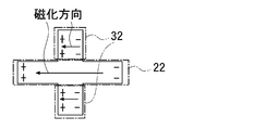
- N pole (+) and S pole ( ⁇ ) appear at both ends of the magnetization direction as shown in FIG.
- the first and second free layers 22 and 32 are connected because the distance between the N pole and the S pole is related to the strength against magnetization reversal when a coercive force or a spin injection current flows
- the first free layer 22 magnetized in the longitudinal direction and the second free layer 32 magnetized in the width direction can be discriminated.
- the free layers of the first and second magnetoresistive elements 11 and 12 are separated and the insulating layer and the fixed layer are connected, and the free layer, the insulating layer, and the fixed layer are all connected.
- the case where the free layer and the insulating layer are separated and the fixed layer is connected, and the case where the free layer, the insulating layer, and the entire fixed layer are separated are also included.
- the fixed layer is separated and the free layer and the insulating layer are connected.
- the case includes a case where the free layer and the fixed layer are separated and the insulating layer is connected, and a case where the insulating layer and the fixed layer are separated and the free layer is connected.
- the fixed layer 48 has an antiferromagnetic layer 47 and a magnetic layer 46, and is formed on a Si substrate 49 in the order of a first electrode 61, an antiferromagnetic layer 47, and a magnetic layer 46.
- the coercive force of the magnetic layer 46 is increased when the magnetic layer 46 and the antiferromagnetic layer 47 are brought into contact with each other.
- the present invention is not limited to the case where the magnetization direction of the fixed layer 48 is fixed by providing the antiferromagnetic layer 47, and the coercive force of the magnetic layer 46 is sufficiently higher than both the first and second coercive forces.
- the antiferromagnetic layer 47 may not be provided.
- the coercive force of the magnetic layer 46 is usually about several tens of gauss, whereas when the magnetization direction is fixed by the antiferromagnetic layer 47, the coercive force increases to about 600 to 800 gauss.
- the difference from the first and second coercive forces can be made larger.
- the constituent material of the antiferromagnetic layer 47 is, for example, PtMn.
- the constituent material of the magnetic layer 46 is, for example, a ferrimagnetic material in which CoFeB / Ru / CoFe is laminated.
- the constituent material of the free layers 22 and 32 is, for example, CoFeB whose coercive force differs by about one digit.
- the constituent material of the insulating layer 43 is not particularly limited. For example, either or both of MgO and alumina (Al 2 O 3 ) can be used. However, when MgO is used, the resistance change rate of the memory element 10 is increased. Particularly preferred.
Landscapes
- Engineering & Computer Science (AREA)
- Computer Hardware Design (AREA)
- Chemical & Material Sciences (AREA)
- Nanotechnology (AREA)
- Physics & Mathematics (AREA)
- Crystallography & Structural Chemistry (AREA)
- Condensed Matter Physics & Semiconductors (AREA)
- General Physics & Mathematics (AREA)
- Mram Or Spin Memory Techniques (AREA)
- Hall/Mr Elements (AREA)
Abstract
記憶容量の高い記憶素子及び記憶方法を提供する。本発明の記憶素子は第一、第二の磁気抵抗素子が並列接続されて構成される。第一、第二の磁気抵抗素子は共通の固定層と、固定層より保磁力の小さい第一、第二の自由層22、32と、固定層と自由層に挟まれた共通の絶縁層を有する。第一、第二の自由層22、32は長手方向と、長手方向より長さの短い幅方向を有する形状をしており、互いの長手方向に沿って延びる直線が直角になるように配置されている。固定層の磁化方向F0と第一、第二の自由層22、32の磁化方向F1、F2は、第一の自由層22の長手方向と平行な方向にされている。長手方向に磁化された第一の自由層22の保磁力は、幅方向に磁化された第二の自由層32の保磁力より小さい。従って、第二の自由層32の磁化方向F2を変えずに、第一の自由層の磁化方向F1を反転させることで、3値又は4値の記憶が可能になっている。
Description
本発明は、記憶素子及び記憶方法に関する。
現在、トンネル磁気抵抗(TMR:Tunneling Magneto-Resistive)効果を発現する磁性多層膜を用いた記憶素子(トンネル磁気抵抗素子)は、MRAM等の不揮発性メモリー等に応用されている。
トンネル磁気抵抗素子の多層膜は、二層の磁性層と、その間に挟まれる絶縁層を有している。絶縁層はアルミナあるいはMgOなどの材料が使用される。
トンネル磁気抵抗素子の多層膜は、二層の磁性層と、その間に挟まれる絶縁層を有している。絶縁層はアルミナあるいはMgOなどの材料が使用される。
絶縁層の膜厚は薄く、記憶素子として動作させるために多層膜面上に垂直にセンス電流を流すと、トンネル効果により、二層の磁性層の間に挟まれる絶縁層を通して各膜の積層に垂直にトンネル電流が流れる。
トンネル磁気抵抗素子の抵抗値は、二層の磁性層の磁化方向が互いに同じ向きの場合に小さく、逆向きの場合に大きい。
従来採用されている矩形あるいは楕円形のトンネル磁気抵抗素子では、大小の抵抗値を『0』『1』に対応させることにより二進法を採用した記憶素子を作製することが可能であった。
トンネル磁気抵抗素子の抵抗値は、二層の磁性層の磁化方向が互いに同じ向きの場合に小さく、逆向きの場合に大きい。
従来採用されている矩形あるいは楕円形のトンネル磁気抵抗素子では、大小の抵抗値を『0』『1』に対応させることにより二進法を採用した記憶素子を作製することが可能であった。
現在研究開発が進められている不揮発性メモリーのMRAMにしても、あるいは量産され更に微細化が進められているDRAMにしても、情報の基本となるビットは『0』『1』の二進法を基本としている。そのためそれが揮発であれ不揮発であれ、容量という観点から見れば優位性はない。
これらの記憶容量を増やすためには記憶素子の個数(密度)を増やすこと以外に解はなく、そのためには微細化をより進める以外に方法はないが、記憶素子の微細化には限界がある。従って、微細化以外の方法で記録密度を向上させるための手段が必要である。
微細化以外の方法として、2値の記憶素子に代わり3値又は4値の記憶素子を作製することが考えられる。一例として、異なる保磁力の磁性層を三層以上積層した多層膜で、異なるトンネル抵抗値を持った磁気抵抗素子を複数直列に接続する方法が考えられるが、その方法では新たに複雑な多層膜を作製する必要があり、コストが高いという問題があった。
本発明は上記従来技術の不都合を解決するために創作されたものであり、その目的は、従来の単純な多層膜構造で3値又は4値を記憶する記憶素子及び記憶方法を提供することにある。
本発明は上記従来技術の不都合を解決するために創作されたものであり、その目的は、従来の単純な多層膜構造で3値又は4値を記憶する記憶素子及び記憶方法を提供することにある。
上記課題を解決するために、本発明は膜厚方向とは垂直な方向に磁化され、所定の保磁力を有する固定層と、前記固定層の磁化方向と平行な方向に磁化され、保磁力が前記固定層よりも小さい自由層と、前記固定層と前記自由層とで挟まれた絶縁層とを有し、前記固定層と前記自由層との間に電圧を印加すると、前記固定層の磁化方向と前記自由層の磁化方向の異同に応じた抵抗値で前記絶縁層にトンネル電流が流れる第一、第二の磁気抵抗素子が並列接続された記憶素子であって、前記第一の磁気抵抗素子の前記自由層の前記磁化方向に沿った長さは、前記第二の磁気抵抗素子の前記自由層の前記磁化方向に沿った長さより長くされ、磁化方向とは逆向きな外部磁界に対し、前記第二の磁気抵抗素子の前記自由層の保磁力は、前記第一の磁気抵抗素子の前記自由層の保磁力よりも大きくされ、抵抗値の大きさで3値又は4値が記憶される記憶素子である。
本発明は、膜厚方向とは垂直な方向に磁化され、所定の保磁力を有する固定層と、前記固定層の磁化方向と平行な方向に磁化され、保磁力が前記固定層よりも小さい自由層と、前記固定層と前記自由層とで挟まれた絶縁層とを有し、前記固定層と前記自由層との間に電圧を印加すると、前記固定層の磁化方向と前記自由層の磁化方向の異同に応じた抵抗値で前記絶縁層にトンネル電流が流れる第一、第二の磁気抵抗素子が並列接続された記憶素子であって、前記第一、第二の磁気抵抗素子がそれぞれ有する前記自由層は、平面形状が、幅と、前記幅よりも長い長手方向とを有する形状に形成され、前記第一、第二の磁気抵抗素子の前記自由層の前記長手方向は互いに直角に配置され、前記第一の磁気抵抗素子の前記自由層は、その前記自由層の前記長手方向と平行に磁化され、前記第二の磁気抵抗素子の前記自由層は、その前記自由層の前記幅の長さ方向と平行に磁化されて、磁化方向とは逆向きな外部磁界に対し、前記第二の磁気抵抗素子の前記自由層の保磁力は、前記第一の磁気抵抗素子の前記自由層の保磁力よりも大きくされ、抵抗値の大きさで3値又は4値が記憶される記憶素子である。
本発明は、膜厚方向とは垂直な方向に磁化され、所定の保磁力を有する固定層と、前記固定層の磁化方向と平行な方向に磁化され、保磁力が前記固定層よりも小さい自由層と、前記固定層と前記自由層とで挟まれた絶縁層とを有し、前記固定層と前記自由層との間に電圧を印加すると、前記固定層の磁化方向と前記自由層の磁化方向の異同に応じた抵抗値で前記絶縁層にトンネル電流が流れる第一、第二の磁気抵抗素子が並列接続された記憶素子であって、前記第一の磁気抵抗素子の前記自由層の前記磁化方向に沿った長さは、前記第二の磁気抵抗素子の前記自由層の前記磁化方向に沿った長さより長くされ、磁化方向を逆向きにするスピン注入電流に対し、前記第二の磁気抵抗素子の前記自由層のスピン注入電流が流れたときの磁化反転に対する強さは、前記第一の磁気抵抗素子の前記自由層のスピン注入電流が流れたときの磁化反転に対する強さよりも大きくされ、抵抗値の大きさで3値又は4値が記憶される記憶素子である。
本発明は、膜厚方向とは垂直な方向に磁化され、所定の保磁力を有する固定層と、前記固定層の磁化方向と平行な方向に磁化され、保磁力が前記固定層よりも小さい自由層と、前記固定層と前記自由層とで挟まれた絶縁層とを有し、前記固定層と前記自由層との間に電圧を印加すると、前記固定層の磁化方向と前記自由層の磁化方向の異同に応じた抵抗値で前記絶縁層にトンネル電流が流れる第一、第二の磁気抵抗素子が並列接続された記憶素子であって、前記第一、第二の磁気抵抗素子がそれぞれ有する前記自由層は、平面形状が、幅と、前記幅よりも長い長手方向とを有する形状に形成され、前記第一、第二の磁気抵抗素子の前記自由層の前記長手方向は互いに直角に配置され、前記第一の磁気抵抗素子の前記自由層は、その前記自由層の前記長手方向と平行に磁化され、前記第二の磁気抵抗素子の前記自由層は、その前記自由層の前記幅の長さ方向と平行に磁化されて、磁化方向を逆向きにするスピン注入電流に対し、前記第二の磁気抵抗素子の前記自由層のスピン注入電流が流れたときの磁化反転に対する強さは、前記第一の磁気抵抗素子の前記自由層のスピン注入電流が流れたときの磁化反転に対する強さよりも大きくされ、抵抗値の大きさで3値又は4値が記憶される記憶素子である。
本発明は記憶素子であって、前記第一、第二の磁気抵抗素子がそれぞれ有する前記自由層は互いに接続されている記憶素子である。
本発明は記憶素子であって、前記第一、第二の磁気抵抗素子がそれぞれ有する前記固定層は互いに接続されている記憶素子である。
本発明は記憶素子であって、前記第一、第二の磁気抵抗素子がそれぞれ有する前記絶縁層は互いに接続されている記憶素子である。
本発明は、前記記憶素子を用いて、第一、第二、第三の値を記憶する記憶方法であって、前記第一の値を記憶するために、前記第一、第二の磁気抵抗素子の両方が磁化同方向抵抗値を示すように、前記第一、第二の磁気抵抗素子の前記自由層の磁化方向をそれぞれ前記固定層の磁化方向と同じ方向に向けて、前記第一、第二の磁気抵抗素子の並列抵抗値を前記第一の値と対応させて記憶し、前記第二の値を記憶するために、前記第一、第二の磁気抵抗素子の両方が磁化反対方向抵抗値を示すように、前記第一、第二の磁気抵抗素子の前記自由層の磁化方向をそれぞれ前記固定層の磁化方向と反対方向に向けて、前記第一、第二の磁気抵抗素子の並列抵抗値を前記第二の値と対応させて記憶し、前記第三の値を記憶するために、いずれか一方の前記磁気抵抗素子が前記磁化同方向抵抗値を示すように当該一方の前記磁気抵抗素子の前記自由層の磁化方向を前記固定層の磁化方向と同じ方向に向け、他方の前記磁気抵抗素子が前記磁化同方向抵抗値を示すように当該他方の前記磁気抵抗素子の前記自由層の磁化方向を前記固定層の磁化方向と反対方向に向けて、前記第一、第二の磁気抵抗素子の並列抵抗値を前記第三の値と対応させて記憶する記憶方法である。
本発明は、第一、第二、第三の値を相互に書き換えて、書き換えた値を記憶する記憶方法であって、前記第一の磁気抵抗素子の前記自由層の磁化方向だけを反転させる場合には、前記第一の磁気抵抗素子の前記自由層の保磁力よりも大きく、前記第二の磁気抵抗素子の前記自由層の保磁力よりも小さい外部磁界を、前記第一の磁気抵抗素子の前記自由層の磁化方向と逆向きに印加して、書き換えた値を記憶する記憶方法である。
本発明は、第一、第二、第三の値を相互に書き換えて、書き換えた値を記憶する記憶方法であって、前記第一の磁気抵抗素子の前記自由層の磁化方向だけを反転させる場合には、前記第一の磁気抵抗素子の前記自由層の磁化方向を逆向きにし、前記第一の磁気抵抗素子の前記自由層のスピン注入電流が流れたときの磁化反転に対する強さよりも大きく、前記第二の磁気抵抗素子の前記自由層のスピン注入電流が流れたときの磁化反転に対する強さよりも小さいスピン注入電流を流して、書き換えた値を記憶する記憶方法である。
本発明は、前記記憶素子の抵抗値を測定し、前記抵抗値から記憶された値を読み取る記憶方法であって、前記記憶素子の抵抗値を測定して基準値と比較し、両方の前記磁気抵抗素子の抵抗値が前記磁化同方向抵抗値であると判別した場合を前記第一の値とし、両方の前記磁気抵抗素子の抵抗値が前記磁化反対方向抵抗値であると判別した場合を前記第二の値とし、一方の前記磁気抵抗素子が前記磁化同方向抵抗値であり他方の前記磁気抵抗素子が前記磁化反対方向抵抗値であると判別した場合を第三の値とする記憶方法である。
本発明は、膜厚方向とは垂直な方向に磁化され、所定の保磁力を有する固定層と、前記固定層の磁化方向と平行な方向に磁化され、保磁力が前記固定層よりも小さい自由層と、前記固定層と前記自由層とで挟まれた絶縁層とを有し、前記固定層と前記自由層との間に電圧を印加すると、前記固定層の磁化方向と前記自由層の磁化方向の異同に応じた抵抗値で前記絶縁層にトンネル電流が流れる第一、第二の磁気抵抗素子が並列接続された記憶素子であって、前記第一、第二の磁気抵抗素子がそれぞれ有する前記自由層は、平面形状が、幅と、前記幅よりも長い長手方向とを有する形状に形成され、前記第一、第二の磁気抵抗素子の前記自由層の前記長手方向は互いに直角に配置され、前記第一の磁気抵抗素子の前記自由層は、その前記自由層の前記長手方向と平行に磁化され、前記第二の磁気抵抗素子の前記自由層は、その前記自由層の前記幅の長さ方向と平行に磁化されて、磁化方向とは逆向きな外部磁界に対し、前記第二の磁気抵抗素子の前記自由層の保磁力は、前記第一の磁気抵抗素子の前記自由層の保磁力よりも大きくされ、抵抗値の大きさで3値又は4値が記憶される記憶素子である。
本発明は、膜厚方向とは垂直な方向に磁化され、所定の保磁力を有する固定層と、前記固定層の磁化方向と平行な方向に磁化され、保磁力が前記固定層よりも小さい自由層と、前記固定層と前記自由層とで挟まれた絶縁層とを有し、前記固定層と前記自由層との間に電圧を印加すると、前記固定層の磁化方向と前記自由層の磁化方向の異同に応じた抵抗値で前記絶縁層にトンネル電流が流れる第一、第二の磁気抵抗素子が並列接続された記憶素子であって、前記第一の磁気抵抗素子の前記自由層の前記磁化方向に沿った長さは、前記第二の磁気抵抗素子の前記自由層の前記磁化方向に沿った長さより長くされ、磁化方向を逆向きにするスピン注入電流に対し、前記第二の磁気抵抗素子の前記自由層のスピン注入電流が流れたときの磁化反転に対する強さは、前記第一の磁気抵抗素子の前記自由層のスピン注入電流が流れたときの磁化反転に対する強さよりも大きくされ、抵抗値の大きさで3値又は4値が記憶される記憶素子である。
本発明は、膜厚方向とは垂直な方向に磁化され、所定の保磁力を有する固定層と、前記固定層の磁化方向と平行な方向に磁化され、保磁力が前記固定層よりも小さい自由層と、前記固定層と前記自由層とで挟まれた絶縁層とを有し、前記固定層と前記自由層との間に電圧を印加すると、前記固定層の磁化方向と前記自由層の磁化方向の異同に応じた抵抗値で前記絶縁層にトンネル電流が流れる第一、第二の磁気抵抗素子が並列接続された記憶素子であって、前記第一、第二の磁気抵抗素子がそれぞれ有する前記自由層は、平面形状が、幅と、前記幅よりも長い長手方向とを有する形状に形成され、前記第一、第二の磁気抵抗素子の前記自由層の前記長手方向は互いに直角に配置され、前記第一の磁気抵抗素子の前記自由層は、その前記自由層の前記長手方向と平行に磁化され、前記第二の磁気抵抗素子の前記自由層は、その前記自由層の前記幅の長さ方向と平行に磁化されて、磁化方向を逆向きにするスピン注入電流に対し、前記第二の磁気抵抗素子の前記自由層のスピン注入電流が流れたときの磁化反転に対する強さは、前記第一の磁気抵抗素子の前記自由層のスピン注入電流が流れたときの磁化反転に対する強さよりも大きくされ、抵抗値の大きさで3値又は4値が記憶される記憶素子である。
本発明は記憶素子であって、前記第一、第二の磁気抵抗素子がそれぞれ有する前記自由層は互いに接続されている記憶素子である。
本発明は記憶素子であって、前記第一、第二の磁気抵抗素子がそれぞれ有する前記固定層は互いに接続されている記憶素子である。
本発明は記憶素子であって、前記第一、第二の磁気抵抗素子がそれぞれ有する前記絶縁層は互いに接続されている記憶素子である。
本発明は、前記記憶素子を用いて、第一、第二、第三の値を記憶する記憶方法であって、前記第一の値を記憶するために、前記第一、第二の磁気抵抗素子の両方が磁化同方向抵抗値を示すように、前記第一、第二の磁気抵抗素子の前記自由層の磁化方向をそれぞれ前記固定層の磁化方向と同じ方向に向けて、前記第一、第二の磁気抵抗素子の並列抵抗値を前記第一の値と対応させて記憶し、前記第二の値を記憶するために、前記第一、第二の磁気抵抗素子の両方が磁化反対方向抵抗値を示すように、前記第一、第二の磁気抵抗素子の前記自由層の磁化方向をそれぞれ前記固定層の磁化方向と反対方向に向けて、前記第一、第二の磁気抵抗素子の並列抵抗値を前記第二の値と対応させて記憶し、前記第三の値を記憶するために、いずれか一方の前記磁気抵抗素子が前記磁化同方向抵抗値を示すように当該一方の前記磁気抵抗素子の前記自由層の磁化方向を前記固定層の磁化方向と同じ方向に向け、他方の前記磁気抵抗素子が前記磁化同方向抵抗値を示すように当該他方の前記磁気抵抗素子の前記自由層の磁化方向を前記固定層の磁化方向と反対方向に向けて、前記第一、第二の磁気抵抗素子の並列抵抗値を前記第三の値と対応させて記憶する記憶方法である。
本発明は、第一、第二、第三の値を相互に書き換えて、書き換えた値を記憶する記憶方法であって、前記第一の磁気抵抗素子の前記自由層の磁化方向だけを反転させる場合には、前記第一の磁気抵抗素子の前記自由層の保磁力よりも大きく、前記第二の磁気抵抗素子の前記自由層の保磁力よりも小さい外部磁界を、前記第一の磁気抵抗素子の前記自由層の磁化方向と逆向きに印加して、書き換えた値を記憶する記憶方法である。
本発明は、第一、第二、第三の値を相互に書き換えて、書き換えた値を記憶する記憶方法であって、前記第一の磁気抵抗素子の前記自由層の磁化方向だけを反転させる場合には、前記第一の磁気抵抗素子の前記自由層の磁化方向を逆向きにし、前記第一の磁気抵抗素子の前記自由層のスピン注入電流が流れたときの磁化反転に対する強さよりも大きく、前記第二の磁気抵抗素子の前記自由層のスピン注入電流が流れたときの磁化反転に対する強さよりも小さいスピン注入電流を流して、書き換えた値を記憶する記憶方法である。
本発明は、前記記憶素子の抵抗値を測定し、前記抵抗値から記憶された値を読み取る記憶方法であって、前記記憶素子の抵抗値を測定して基準値と比較し、両方の前記磁気抵抗素子の抵抗値が前記磁化同方向抵抗値であると判別した場合を前記第一の値とし、両方の前記磁気抵抗素子の抵抗値が前記磁化反対方向抵抗値であると判別した場合を前記第二の値とし、一方の前記磁気抵抗素子が前記磁化同方向抵抗値であり他方の前記磁気抵抗素子が前記磁化反対方向抵抗値であると判別した場合を第三の値とする記憶方法である。
本発明は、磁性層の磁化方向が外部磁界の方向と平行であり、長軸が短軸より長い(ここでは1.5倍以上長いとする)場合に、磁化方向が長軸に平行な磁性層は、磁化方向が短軸に平行な磁性層よりも小さな外部磁界で磁化方向を反転させることができること(磁気形状異方性という)に着目している。
磁性層が磁化した状態は磁性層の磁化方向の両端にN極とS極が現れた状態であり、この磁極は磁性層外部に磁力線を発生させるのと同時に、磁性層内部にも外部とは反対方向に磁場(反磁場)を作る。内部の反磁場の大きさは、磁化の大きさに比例すると同時に、磁化方向の形状に依存し、長矩形状の磁性層では長軸方向に磁化した場合が一番小さい(無限に長い棒では反磁場が0になる)。磁性層の内部に働く磁場は、外部磁界と反磁場の差で与えられると考えられる。
図3(a)、(b)は、長軸、短軸に平行な方向に磁化された磁性層に、磁化方向と平行で逆向きの外部磁界を印加したときの、外部磁界の強度と磁性層の磁化の関係を測定した結果である。
長軸に平行な方向に磁化された磁性層は、弱い外部磁界±H1で反転して磁化が飽和するが(図3(a))、短軸に平行な方向に磁化された磁性層は、±H1よりも大きな±H2で反転するまで直線的に磁化が変化するので、大きな外部磁界をかけないと磁化が飽和しない(図3(b))。
長軸に平行な方向に磁化された磁性層は、弱い外部磁界±H1で反転して磁化が飽和するが(図3(a))、短軸に平行な方向に磁化された磁性層は、±H1よりも大きな±H2で反転するまで直線的に磁化が変化するので、大きな外部磁界をかけないと磁化が飽和しない(図3(b))。
また、本発明は、第一、第二の磁気抵抗素子の自由層の面積比を制御することにより、一方の磁気抵抗素子の自由層と固定層の磁化方向が同方向で、他方の磁気抵抗素子の自由層と固定層の磁化方向が逆方向のときの抵抗値を、両方の磁気抵抗素子の自由層と固定層の磁化方向が同方向のときの抵抗値と、両方の磁気抵抗素子の自由層と固定層の磁化方向が逆方向のときの抵抗値に対して制御できる記憶素子である。
磁化形状異方性を持つ形状のトンネル磁気抵抗素子を二個並列に接続することで、抵抗値は最大値、最小値以外に、一方の素子の二層の磁性層の磁場が互いに同方向で他方の素子の二層の磁性層の磁場が互いに逆方向のときに中間値を取ることができ、最大値、中間値、最小値を判別することで3値又は4値の記憶素子が得られる。
従って、記憶素子の密度を増やさなくても、2値の記憶媒体よりも記憶容量を増やすことができる。
また従来から使用されている多層膜が利用できるため、新たに複雑な積層構造の多層膜を作製する必要はなく、低コストで3値又は4値の記憶素子が得られる。
また従来から使用されている多層膜が利用できるため、新たに複雑な積層構造の多層膜を作製する必要はなく、低コストで3値又は4値の記憶素子が得られる。
1……記憶装置
10……記憶素子
11……第一の磁気抵抗素子
12……第二の磁気抵抗素子
22……第一の磁気抵抗素子の自由層
32……第二の磁気抵抗素子の自由層
43……絶縁層
48……固定層
51……第一の磁気抵抗素子の自由層の長手方向
52……第一の磁気抵抗素子の自由層の幅の長さ方向
53……第二の磁気抵抗素子の自由層の長手方向
54……第二の磁気抵抗素子の自由層の幅の長さ方向
10……記憶素子
11……第一の磁気抵抗素子
12……第二の磁気抵抗素子
22……第一の磁気抵抗素子の自由層
32……第二の磁気抵抗素子の自由層
43……絶縁層
48……固定層
51……第一の磁気抵抗素子の自由層の長手方向
52……第一の磁気抵抗素子の自由層の幅の長さ方向
53……第二の磁気抵抗素子の自由層の長手方向
54……第二の磁気抵抗素子の自由層の幅の長さ方向
図1の符号10は本発明である記憶素子の平面図である。記憶素子10は第一、第二の磁気抵抗素子11、12を有している。
図2は記憶素子10のA-A切断断面図である。
第一、第二の磁気抵抗素子11、12は、所定の保磁力を有する固定層48と、絶縁層43と、固定層48の磁化方向と平行な方向に磁化され、保磁力が固定層48より小さい自由層22、32を有している。
図2は記憶素子10のA-A切断断面図である。
第一、第二の磁気抵抗素子11、12は、所定の保磁力を有する固定層48と、絶縁層43と、固定層48の磁化方向と平行な方向に磁化され、保磁力が固定層48より小さい自由層22、32を有している。
第一の電極61と固定層48と絶縁層43と自由層22、32とをこの順序でSi基板49上に積層した後、自由層22、32部分だけを後述の形状にエッチングして、第一、第二の磁気抵抗素子11、12が形成されている。
自由層22、32のエッチング後、自由層22、32側からSiO2層41を積層し、その後にSiO2層41をエッチングして自由層22、32の表面を露出させる。自由層22、32の表面に密着するように第二の電極62を形成する。
自由層22、32のエッチング後、自由層22、32側からSiO2層41を積層し、その後にSiO2層41をエッチングして自由層22、32の表面を露出させる。自由層22、32の表面に密着するように第二の電極62を形成する。
絶縁層43の膜厚は薄く、自由層22、32と固定層48との間に電圧が印加されると、トンネル効果により、各層に対して垂直な方向にトンネル電流が流れる。
トンネル電流が流れるときの第一、第二の磁気抵抗素子11、12のコンダクタンス値は、固定層48の磁化方向に対して、自由層22、32の磁化方向が同じ向きの場合に大きく、逆向きの場合に小さい(コンダクタンス値は抵抗値の逆数である)。従って、第一、第二の磁気抵抗素子11、12はトンネル磁気抵抗素子として機能する。
トンネル電流が流れるときの第一、第二の磁気抵抗素子11、12のコンダクタンス値は、固定層48の磁化方向に対して、自由層22、32の磁化方向が同じ向きの場合に大きく、逆向きの場合に小さい(コンダクタンス値は抵抗値の逆数である)。従って、第一、第二の磁気抵抗素子11、12はトンネル磁気抵抗素子として機能する。
第一、第二の磁気抵抗素子11、12の自由層22、32(以下第一、第二の自由層と呼ぶ)の平面形状は、図1に示すように、長手方向51、53とそれに垂直で長手方向の長さより短い幅方向52、54を有している。ここでは、第一の自由層22の長手方向51の長さは、幅方向52の長さの1.5倍以上とする。
第一、第二の自由層22、32は互いに平行な方向に磁化されている。
第一の自由層22の磁化方向に沿った長さは、第二の自由層32の磁化方向に沿った長さより長くされ、ここでは、第一、第二の自由層22、32は、長手方向51、53が互いに直角になるように配置されている。
そのため、磁化方向とは逆向きな外部磁界に対し、長手方向51に磁化された第一の自由層22の保磁力(以下第一の保磁力と呼ぶ)は、幅方向54に磁化された第二の自由層32の保磁力(以下第二の保磁力と呼ぶ)より小さくされている。また、磁化方向を逆向きにするスピン注入電流に対し、長手方向51に磁化された第一の自由層22のスピン注入電流が流れたときの磁化反転に対する強さは、幅方向54に磁化された第二の自由層32のスピン注入電流が流れたときの磁化反転に対する強さより小さくされている。
ここでは、第一、第二の自由層22、32は、長手方向51、53が互いに直角になるように配置されているが、本発明はこれに限定されず、第一、第二の自由層22、32は、長手方向51、53に沿って延びる直線が互いに交差するように配置されている場合は本発明に含まれる。
第一、第二の自由層22、32は互いに平行な方向に磁化されている。
第一の自由層22の磁化方向に沿った長さは、第二の自由層32の磁化方向に沿った長さより長くされ、ここでは、第一、第二の自由層22、32は、長手方向51、53が互いに直角になるように配置されている。
そのため、磁化方向とは逆向きな外部磁界に対し、長手方向51に磁化された第一の自由層22の保磁力(以下第一の保磁力と呼ぶ)は、幅方向54に磁化された第二の自由層32の保磁力(以下第二の保磁力と呼ぶ)より小さくされている。また、磁化方向を逆向きにするスピン注入電流に対し、長手方向51に磁化された第一の自由層22のスピン注入電流が流れたときの磁化反転に対する強さは、幅方向54に磁化された第二の自由層32のスピン注入電流が流れたときの磁化反転に対する強さより小さくされている。
ここでは、第一、第二の自由層22、32は、長手方向51、53が互いに直角になるように配置されているが、本発明はこれに限定されず、第一、第二の自由層22、32は、長手方向51、53に沿って延びる直線が互いに交差するように配置されている場合は本発明に含まれる。
記憶素子10内部では、図2に示すように、固定層48は第一の電極61に接触して電気的に接続され、第一、第二の自由層22、32はそれぞれ第二の電極62に接触して電気的に接続されている。
従って、記憶素子10は、第一、第二の磁気抵抗素子11、12を並列に接続した並列接続回路を形成している。
従って、記憶素子10は、第一、第二の磁気抵抗素子11、12を並列に接続した並列接続回路を形成している。
第一、第二の電極61、62の間に電圧を印加すると、電流は第一、第二の磁気抵抗素子11、12の両方を膜厚方向と平行な方向に流れるように配線されているが、よりコンダクタンス値の高い部分を流れる傾向を持つ。
第一、第二の磁気抵抗素子11、12のコンダクタンスの最小値をそれぞれC1、C2、最大値をそれぞれC1+ΔC1、C2+ΔC2とする。
第一、第二の磁気抵抗素子11、12のコンダクタンスの最小値をそれぞれC1、C2、最大値をそれぞれC1+ΔC1、C2+ΔC2とする。
図4(a)~(d)は、記憶素子10内部の、固定層48の磁化方向F0に対する、第一、第二の自由層22、32の磁化方向F1、F2の変化を示している。
図4(a)を参照し、第一、第二の自由層22、32の磁化方向F1、F2の両方が、固定層48の磁化方向F0と同じ向きの場合、記憶素子10のコンダクタンス値はC1+C2+ΔC1+ΔC2で表される値に近い最大値となる(低コンダクタンスになった部分を本来流れる電流が高コンダクタンス部に流れ込むため、素子全体としてのコンダクタンス変化は正確にはΔC1+ΔC2とはならず、それに近い値となる)。
図4(a)を参照し、第一、第二の自由層22、32の磁化方向F1、F2の両方が、固定層48の磁化方向F0と同じ向きの場合、記憶素子10のコンダクタンス値はC1+C2+ΔC1+ΔC2で表される値に近い最大値となる(低コンダクタンスになった部分を本来流れる電流が高コンダクタンス部に流れ込むため、素子全体としてのコンダクタンス変化は正確にはΔC1+ΔC2とはならず、それに近い値となる)。
次に、第一の保磁力以上第二の保磁力未満の外部磁界Hrを固定層48の磁化方向F0と逆向きに印加すると、第一の自由層22の磁化方向F1だけが反転し、記憶素子10のコンダクタンス値はC1+C2+ΔC2になる(図4(b))。
次に、第二の保磁力以上の外部磁界Hrを固定層48の磁化方向F0と逆向きに印加すると、第二の自由層32の磁化方向F2も反転し、記憶素子10のコンダクタンス値は最小値C1+C2になる(図4(c))。
次に、第一の保磁力以上第二の保磁力未満の外部磁界Hrを固定層48の磁場方向F0と同じ向きに印加すると、第一の自由層22の磁化方向F1が再度反転して、記憶素子10のコンダクタンス値はC1+C2+ΔC1になる(図4(d))。
次に、第二の保磁力以上の外部磁界Hrを固定層48の磁化方向F0と逆向きに印加すると、第二の自由層32の磁化方向F2も反転し、記憶素子10のコンダクタンス値は最小値C1+C2になる(図4(c))。
次に、第一の保磁力以上第二の保磁力未満の外部磁界Hrを固定層48の磁場方向F0と同じ向きに印加すると、第一の自由層22の磁化方向F1が再度反転して、記憶素子10のコンダクタンス値はC1+C2+ΔC1になる(図4(d))。
このように、記憶素子10のコンダクタンスは、最大値C1+C2+ΔC1+ΔC2、第一の中間値C1+C2+ΔC1、第二の中間値C1+C2+ΔC2、最小値C1+C2の4通りのコンダクタンス値をとる。
第一のコンダクタンス差ΔC1が第二のコンダクタンス差ΔC2より大きい場合(ΔC1>ΔC2)には、第一の中間値が大なる中間値になり、第二の中間値が小なる中間値になる。第一のコンダクタンス差ΔC1が第二のコンダクタンス差ΔC2より小さい場合(ΔC1<ΔC2)には、第二の中間値が大なる中間値になり、第一の中間値が小なる中間値になる。
第一のコンダクタンス差ΔC1が第二のコンダクタンス差ΔC2より大きい場合(ΔC1>ΔC2)には、第一の中間値が大なる中間値になり、第二の中間値が小なる中間値になる。第一のコンダクタンス差ΔC1が第二のコンダクタンス差ΔC2より小さい場合(ΔC1<ΔC2)には、第二の中間値が大なる中間値になり、第一の中間値が小なる中間値になる。
最大値と大なる中間値の間に第一の基準値を置き、小なる中間値と最小値の間に第二の基準値を置いて、最大値、最小値、中間値の3通りのコンダクタンス値を判別することで3値の記憶素子が得られる。
更に、第一、第二の基準値に加えて、大なる中間値と小なる中間値の間に第三の基準値を置いて、最大値、大なる中間値、小なる中間値、最小値の4通りのコンダクタンス値を判別することで4値の記憶素子が得られる。
更に、第一、第二の基準値に加えて、大なる中間値と小なる中間値の間に第三の基準値を置いて、最大値、大なる中間値、小なる中間値、最小値の4通りのコンダクタンス値を判別することで4値の記憶素子が得られる。
次に、本発明の記憶素子10を用いた記憶装置を説明する。図5はMRAM等の記憶装置1の一例を示す断面図である。
記憶装置1は第一、第二の配線5、6を複数本ずつ有している。第一の配線5は所定間隔を空けて互いに平行に配置され、第二の配線6は第一の配線5が配置された平面と平行な平面内で、第一の配線5と交差するように配置されている。ここでは、第一、第二の配線5、6はSiO2等の絶縁層2に埋設されている。
記憶装置1は第一、第二の配線5、6を複数本ずつ有している。第一の配線5は所定間隔を空けて互いに平行に配置され、第二の配線6は第一の配線5が配置された平面と平行な平面内で、第一の配線5と交差するように配置されている。ここでは、第一、第二の配線5、6はSiO2等の絶縁層2に埋設されている。
第一、第二の配線5、6の立体交差位置の近傍には、本発明の記憶素子10が配置されている。第一、第二の配線5、6の交差位置は行列状に配置されているから、記憶素子10は行列状に配置されている。
記憶素子10の第一、第二の電極61、62は、記憶素子10の近傍で交差する第一、第二の配線5、6にそれぞれ接続されている。
第一、第二の配線5、6は制御装置8に接続されている。記憶素子10から記憶された情報を読み出す場合、制御装置8は、第一、第二の配線5、6を選択して所望の記憶素子10に電流を流し、測定装置9は電流が流れた記憶素子10の電極間の電圧と電流から、ここではコンダクタンス値を測定し、測定結果を制御装置8へ伝送する。
記憶素子10の第一、第二の電極61、62は、記憶素子10の近傍で交差する第一、第二の配線5、6にそれぞれ接続されている。
第一、第二の配線5、6は制御装置8に接続されている。記憶素子10から記憶された情報を読み出す場合、制御装置8は、第一、第二の配線5、6を選択して所望の記憶素子10に電流を流し、測定装置9は電流が流れた記憶素子10の電極間の電圧と電流から、ここではコンダクタンス値を測定し、測定結果を制御装置8へ伝送する。
上述したように、本発明の記憶素子10のコンダクタンス値は、最大値、最小値、中間値の3通りが得られ、制御装置8には少なくともコンダクタンスの最大値と最小値が基準値として設定されている。
制御装置8は測定装置9の測定結果と設定されたコンダクタンス値(基準値)とを比較し、測定結果が最大値、最小値、又は最大値と最小値の間(中間値)のいずれに相当するか判断する。制御装置8は、判断した結果をそれぞれ『0』『1』『2』等の情報に関連付け、情報として読み出す。
従って、この記憶装置1では、第一、第二の配線5、6と、制御装置8と、測定装置9とで、情報を読み出す読み出し手段が構成される。
制御装置8は測定装置9の測定結果と設定されたコンダクタンス値(基準値)とを比較し、測定結果が最大値、最小値、又は最大値と最小値の間(中間値)のいずれに相当するか判断する。制御装置8は、判断した結果をそれぞれ『0』『1』『2』等の情報に関連付け、情報として読み出す。
従って、この記憶装置1では、第一、第二の配線5、6と、制御装置8と、測定装置9とで、情報を読み出す読み出し手段が構成される。
次に、情報の書き換えについて説明する。この記憶装置1では、第一の配線5の配線に沿って書き換え配線4が延設されている。第一の配線5は第二の配線6と交差するから、書き換え配線4も第二の配線6と交差する。
各記憶素子10は書き換え配線4と第二の配線6の交差位置で、書き換え配線4と第二の配線6の間に配置されている。書き換え配線4は記憶素子10及び第一、第二の配線5、6と非接触であり、絶縁されている。
各記憶素子10は書き換え配線4と第二の配線6の交差位置で、書き換え配線4と第二の配線6の間に配置されている。書き換え配線4は記憶素子10及び第一、第二の配線5、6と非接触であり、絶縁されている。
書き換え配線4は制御装置8に接続されている。制御装置8には、書き換え配線4及び第二の配線6と、記憶素子10との位置関係が設定されている。
制御装置8は格子状に配置された書き換え配線4と第二の配線6との間に配置されている中で目的とする記憶素子10の一つを選択し、通電する。通電により、書き換え配線4と第二の配線6の周囲に磁場が発生し、書き換え配線4と第二の配線6の交差位置近傍に合成磁場が発生し、他の素子には磁場の影響を与えない。従って、行列状に配置された複数の記憶素子10のうち、選択した配線4、6の交差位置にある記憶素子10だけが合成磁場に曝される。
制御装置8は格子状に配置された書き換え配線4と第二の配線6との間に配置されている中で目的とする記憶素子10の一つを選択し、通電する。通電により、書き換え配線4と第二の配線6の周囲に磁場が発生し、書き換え配線4と第二の配線6の交差位置近傍に合成磁場が発生し、他の素子には磁場の影響を与えない。従って、行列状に配置された複数の記憶素子10のうち、選択した配線4、6の交差位置にある記憶素子10だけが合成磁場に曝される。
書き換え配線4と第二の配線6に流す電流の向きや強さ等の通電条件を変えると、合成磁場の向きや強さが変わる。記憶素子10のコンダクタンスを最大値、最小値、中間値にする各合成磁場を作る通電条件は予め求められ、制御装置8に設定されている。
制御装置8は記憶したい情報と記憶素子10のコンダクタンスを関連付け、コンダクタンスを関連付けた値にする通電条件で、書き換え配線4と第二の配線6に電流を流し、記憶素子10に所望の記憶情報をコンダクタンスとして記憶する。
制御装置8は記憶したい情報と記憶素子10のコンダクタンスを関連付け、コンダクタンスを関連付けた値にする通電条件で、書き換え配線4と第二の配線6に電流を流し、記憶素子10に所望の記憶情報をコンダクタンスとして記憶する。
このように、第二の配線6と、書き換え配線4と、制御装置8とが情報を書き換える書き換え手段となるが、書き換え手段はこれに限定されない。例えば、書き換え手段を書き換え配線4と制御装置8だけで構成してもよい。この場合、制御装置8は書き換え配線4を選択して通電し、選択した書き換え配線4上にある記憶素子10の情報を書き換える。
また、書き換え配線4を設けず、第一、第二の配線5、6と制御装置8で書き換え手段を構成してもよい。この場合、制御装置8は、第一、第二の配線5、6を選択して通電し、選択された第一、第二の配線5、6の交差位置で合成磁場を発生させ、当該交差位置近傍の記憶素子10の情報を書き換える。
また、第一、第二の配線5、6と制御装置8で書き換え手段を構成する場合には、制御装置8は、第一、第二の配線5、6を選択し、磁化を反転させるスピン注入電流を流して、記憶素子10の情報を書き換えてもよい。
第一の自由層の磁化方向だけを反転させる場合には、第一の自由層の磁化方向を逆向きにし、第一の自由層のスピン注入電流が流れたときの磁化反転に対する強さよりも大きく、第二の自由層のスピン注入電流が流れたときの磁化反転に対する強さよりも小さいスピン注入電流を流して、記憶素子10の情報を書き換える。
スピン注入電流を用いることにより、書き換えのために外部磁場を発生させる必要がなく、装置設計の自由度が上がる。
要するに、書き換え手段は制御装置8と配線とを有し、制御装置8が配線を選択して通電することにより、配線上の記憶素子10の情報を書き換える。
第一の自由層の磁化方向だけを反転させる場合には、第一の自由層の磁化方向を逆向きにし、第一の自由層のスピン注入電流が流れたときの磁化反転に対する強さよりも大きく、第二の自由層のスピン注入電流が流れたときの磁化反転に対する強さよりも小さいスピン注入電流を流して、記憶素子10の情報を書き換える。
スピン注入電流を用いることにより、書き換えのために外部磁場を発生させる必要がなく、装置設計の自由度が上がる。
要するに、書き換え手段は制御装置8と配線とを有し、制御装置8が配線を選択して通電することにより、配線上の記憶素子10の情報を書き換える。
書き換え手段は記憶装置1に設ける必要も無い。書き換え手段(例えばごく微少な電磁石等の磁界形成手段)を記憶装置1の外側に設け、書き換えの必要な記憶素子10に外部から書き換え手段を近づけることで、情報の書き換えを行ってもよい。
上記説明では記憶素子10の電極間の電圧と電流から、コンダクタンス値を測定して3値又は4値を判別したが、抵抗値を測定して3値又は4値を判別する場合も本発明に含まれる。また、記憶素子10の電極間の電圧値又は電流値から、3値又は4値を判別してもよい。
なお、固定層48の磁化方向に対して、第一、第二の自由層22、32の磁化方向が同じ向きの場合の第一、第二の磁気抵抗素子11、12の抵抗値を磁化同方向抵抗値と呼び、逆向きの場合の抵抗値を磁化反対方向抵抗値と呼ぶ。
上記説明では記憶素子10の電極間の電圧と電流から、コンダクタンス値を測定して3値又は4値を判別したが、抵抗値を測定して3値又は4値を判別する場合も本発明に含まれる。また、記憶素子10の電極間の電圧値又は電流値から、3値又は4値を判別してもよい。
なお、固定層48の磁化方向に対して、第一、第二の自由層22、32の磁化方向が同じ向きの場合の第一、第二の磁気抵抗素子11、12の抵抗値を磁化同方向抵抗値と呼び、逆向きの場合の抵抗値を磁化反対方向抵抗値と呼ぶ。
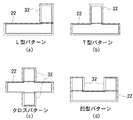
本発明は、第一、第二の自由層22、32が分離されている場合に限定されず、例えば図6(a)~(d)に示すL型パターン、T型パターン、クロスパターン、凹型パターンのように、接続されている場合も含まれる。
例えばクロスパターンの磁性層が磁化されている場合は、図7に示すように磁化方向の両端にN極(+)とS極(-)が現れる。N極とS極との間の距離が保磁力又はスピン注入電流が流れたときの磁化反転に対する強さと関係しているため、第一、第二の自由層22、32が接続されている場合でも、長手方向に磁化された第一の自由層22と幅方向に磁化された第二の自由層32が判別できる。
例えばクロスパターンの磁性層が磁化されている場合は、図7に示すように磁化方向の両端にN極(+)とS極(-)が現れる。N極とS極との間の距離が保磁力又はスピン注入電流が流れたときの磁化反転に対する強さと関係しているため、第一、第二の自由層22、32が接続されている場合でも、長手方向に磁化された第一の自由層22と幅方向に磁化された第二の自由層32が判別できる。
本発明は、第一、第二の磁気抵抗素子11、12の自由層が分離し、絶縁層と固定層が接続している場合と、自由層と絶縁層と固定層の全層が接続している場合に限定されず、自由層と絶縁層が分離し、固定層が接続している場合と、自由層と絶縁層と固定層の全層が分離している場合も含まれる。
また、第一、第二の磁気抵抗素子11、12の絶縁層が分離し、自由層と固定層が接続されている場合と、固定層が分離し、自由層と絶縁層が接続されている場合と、自由層と固定層が分離し、絶縁層が接続されている場合と、絶縁層と固定層が分離し、自由層が接続されている場合も含まれる。
また、第一、第二の磁気抵抗素子11、12の絶縁層が分離し、自由層と固定層が接続されている場合と、固定層が分離し、自由層と絶縁層が接続されている場合と、自由層と固定層が分離し、絶縁層が接続されている場合と、絶縁層と固定層が分離し、自由層が接続されている場合も含まれる。
ここでは、固定層48は反強磁性層47と磁性層46を有しており、Si基板49上に第一の電極61,反強磁性層47、磁性層46の順で形成されている。磁性層46を磁性層の表面と平行な方向に磁化させる場合、磁性層46と反強磁性層47を接触させると磁性層46の保磁力が増大される。
本発明は、固定層48の磁化方向を反強磁性層47を設けて固定する場合に限定されず、磁性層46の保磁力が、第一、第二の保磁力の両方より十分高いのであれば、反強磁性層47を設けなくてもよい。
本発明は、固定層48の磁化方向を反強磁性層47を設けて固定する場合に限定されず、磁性層46の保磁力が、第一、第二の保磁力の両方より十分高いのであれば、反強磁性層47を設けなくてもよい。
しかし、通常、磁性層46の保磁力は数十ガウス程度であるのに対し、反強磁性層47で磁化方向を固定した場合には、保磁力が600ガウス~800ガウス程度に上昇するので、反強磁性層47で磁化方向を固定した方が、第一、第二の保磁力との差をより大きくできる。
反強磁性層47の構成材料は例えばPtMn等である。磁性層46の構成材料は例えばCoFeB/Ru/CoFeを積層したフェリ磁性体等である。自由層22、32の構成材料は保磁力が1桁程度異なる、例えばCoFeBである。
絶縁層43の構成材料は特に限定されず、例えばMgOやアルミナ(Al2O3)のいずれか一方又は両方を用いることができるが、MgOを用いると記憶素子10の抵抗変化率が高くなるから特に好ましい。
絶縁層43の構成材料は特に限定されず、例えばMgOやアルミナ(Al2O3)のいずれか一方又は両方を用いることができるが、MgOを用いると記憶素子10の抵抗変化率が高くなるから特に好ましい。
Claims (11)
- 膜厚方向とは垂直な方向に磁化され、所定の保磁力を有する固定層と、
前記固定層の磁化方向と平行な方向に磁化され、保磁力が前記固定層よりも小さい自由層と、
前記固定層と前記自由層とで挟まれた絶縁層とを有し、
前記固定層と前記自由層との間に電圧を印加すると、前記固定層の磁化方向と前記自由層の磁化方向の異同に応じた抵抗値で前記絶縁層にトンネル電流が流れる第一、第二の磁気抵抗素子が並列接続された記憶素子であって、
前記第一の磁気抵抗素子の前記自由層の前記磁化方向に沿った長さは、前記第二の磁気抵抗素子の前記自由層の前記磁化方向に沿った長さより長くされ、
磁化方向とは逆向きな外部磁界に対し、前記第二の磁気抵抗素子の前記自由層の保磁力は、前記第一の磁気抵抗素子の前記自由層の保磁力よりも大きくされ、抵抗値の大きさで3値又は4値が記憶される記憶素子。 - 膜厚方向とは垂直な方向に磁化され、所定の保磁力を有する固定層と、
前記固定層の磁化方向と平行な方向に磁化され、保磁力が前記固定層よりも小さい自由層と、
前記固定層と前記自由層とで挟まれた絶縁層とを有し、
前記固定層と前記自由層との間に電圧を印加すると、前記固定層の磁化方向と前記自由層の磁化方向の異同に応じた抵抗値で前記絶縁層にトンネル電流が流れる第一、第二の磁気抵抗素子が並列接続された記憶素子であって、
前記第一、第二の磁気抵抗素子がそれぞれ有する前記自由層は、平面形状が、幅と、前記幅よりも長い長手方向とを有する形状に形成され、前記第一、第二の磁気抵抗素子の前記自由層の前記長手方向は互いに直角に配置され、
前記第一の磁気抵抗素子の前記自由層は、その前記自由層の前記長手方向と平行に磁化され、
前記第二の磁気抵抗素子の前記自由層は、その前記自由層の前記幅の長さ方向と平行に磁化されて、
磁化方向とは逆向きな外部磁界に対し、前記第二の磁気抵抗素子の前記自由層の保磁力は、前記第一の磁気抵抗素子の前記自由層の保磁力よりも大きくされ、抵抗値の大きさで3値又は4値が記憶される記憶素子。 - 膜厚方向とは垂直な方向に磁化され、所定の保磁力を有する固定層と、
前記固定層の磁化方向と平行な方向に磁化され、保磁力が前記固定層よりも小さい自由層と、
前記固定層と前記自由層とで挟まれた絶縁層とを有し、
前記固定層と前記自由層との間に電圧を印加すると、前記固定層の磁化方向と前記自由層の磁化方向の異同に応じた抵抗値で前記絶縁層にトンネル電流が流れる第一、第二の磁気抵抗素子が並列接続された記憶素子であって、
前記第一の磁気抵抗素子の前記自由層の前記磁化方向に沿った長さは、前記第二の磁気抵抗素子の前記自由層の前記磁化方向に沿った長さより長くされ、
磁化方向を逆向きにするスピン注入電流に対し、前記第二の磁気抵抗素子の前記自由層のスピン注入電流が流れたときの磁化反転に対する強さは、前記第一の磁気抵抗素子の前記自由層のスピン注入電流が流れたときの磁化反転に対する強さよりも大きくされ、抵抗値の大きさで3値又は4値が記憶される記憶素子。 - 膜厚方向とは垂直な方向に磁化され、所定の保磁力を有する固定層と、
前記固定層の磁化方向と平行な方向に磁化され、保磁力が前記固定層よりも小さい自由層と、
前記固定層と前記自由層とで挟まれた絶縁層とを有し、
前記固定層と前記自由層との間に電圧を印加すると、前記固定層の磁化方向と前記自由層の磁化方向の異同に応じた抵抗値で前記絶縁層にトンネル電流が流れる第一、第二の磁気抵抗素子が並列接続された記憶素子であって、
前記第一、第二の磁気抵抗素子がそれぞれ有する前記自由層は、平面形状が、幅と、前記幅よりも長い長手方向とを有する形状に形成され、前記第一、第二の磁気抵抗素子の前記自由層の前記長手方向は互いに直角に配置され、
前記第一の磁気抵抗素子の前記自由層は、その前記自由層の前記長手方向と平行に磁化され、
前記第二の磁気抵抗素子の前記自由層は、その前記自由層の前記幅の長さ方向と平行に磁化されて、
磁化方向を逆向きにするスピン注入電流に対し、前記第二の磁気抵抗素子の前記自由層のスピン注入電流が流れたときの磁化反転に対する強さは、前記第一の磁気抵抗素子の前記自由層のスピン注入電流が流れたときの磁化反転に対する強さよりも大きくされ、抵抗値の大きさで3値又は4値が記憶される記憶素子。 - 前記第一、第二の磁気抵抗素子がそれぞれ有する前記自由層は互いに接続されている請求項1乃至請求項4のいずれか1項記載の記憶素子。
- 前記第一、第二の磁気抵抗素子がそれぞれ有する前記固定層は互いに接続されている請求項1乃至請求項5のいずれか1項記載の記憶素子。
- 前記第一、第二の磁気抵抗素子がそれぞれ有する前記絶縁層は互いに接続されている請求項1乃至請求項6のいずれか1項記載の記憶素子。
- 請求項1乃至請求項7のいずれか1項記載の記憶素子を用いて、第一、第二、第三の値を記憶する記憶方法であって、
前記第一の値を記憶するために、前記第一、第二の磁気抵抗素子の両方が磁化同方向抵抗値を示すように、前記第一、第二の磁気抵抗素子の前記自由層の磁化方向をそれぞれ前記固定層の磁化方向と同じ方向に向けて、前記第一、第二の磁気抵抗素子の並列抵抗値を前記第一の値と対応させて記憶し、
前記第二の値を記憶するために、前記第一、第二の磁気抵抗素子の両方が磁化反対方向抵抗値を示すように、前記第一、第二の磁気抵抗素子の前記自由層の磁化方向をそれぞれ前記固定層の磁化方向と反対方向に向けて、前記第一、第二の磁気抵抗素子の並列抵抗値を前記第二の値と対応させて記憶し、
前記第三の値を記憶するために、いずれか一方の前記磁気抵抗素子が前記磁化同方向抵抗値を示すように当該一方の前記磁気抵抗素子の前記自由層の磁化方向を前記固定層の磁化方向と同じ方向に向け、他方の前記磁気抵抗素子が前記磁化同方向抵抗値を示すように当該他方の前記磁気抵抗素子の前記自由層の磁化方向を前記固定層の磁化方向と反対方向に向けて、前記第一、第二の磁気抵抗素子の並列抵抗値を前記第三の値と対応させて記憶する記憶方法。 - 第一、第二、第三の値を相互に書き換えて、書き換えた値を記憶する請求項8記載の記憶方法であって、
前記第一の磁気抵抗素子の前記自由層の磁化方向だけを反転させる場合には、前記第一の磁気抵抗素子の前記自由層の保磁力よりも大きく、前記第二の磁気抵抗素子の前記自由層の保磁力よりも小さい外部磁界を、前記第一の磁気抵抗素子の前記自由層の磁化方向と逆向きに印加して、書き換えた値を記憶する記憶方法。 - 第一、第二、第三の値を相互に書き換えて、書き換えた値を記憶する請求項8記載の記憶方法であって、
前記第一の磁気抵抗素子の前記自由層の磁化方向だけを反転させる場合には、前記第一の磁気抵抗素子の前記自由層の磁化方向を逆向きにし、前記第一の磁気抵抗素子の前記自由層のスピン注入電流が流れたときの磁化反転に対する強さよりも大きく、前記第二の磁気抵抗素子の前記自由層のスピン注入電流が流れたときの磁化反転に対する強さよりも小さいスピン注入電流を流して、書き換えた値を記憶する記憶方法。 - 前記記憶素子の抵抗値を測定し、前記抵抗値から記憶された値を読み取る請求項8記載の記憶方法であって、
前記記憶素子の抵抗値を測定して基準値と比較し、
両方の前記磁気抵抗素子の抵抗値が前記磁化同方向抵抗値であると判別した場合を前記第一の値とし、
両方の前記磁気抵抗素子の抵抗値が前記磁化反対方向抵抗値であると判別した場合を前記第二の値とし、
一方の前記磁気抵抗素子が前記磁化同方向抵抗値であり他方の前記磁気抵抗素子が前記磁化反対方向抵抗値であると判別した場合を第三の値とする記憶方法。
Applications Claiming Priority (2)
| Application Number | Priority Date | Filing Date | Title |
|---|---|---|---|
| JP2009-114010 | 2009-05-08 | ||
| JP2009114010 | 2009-05-08 |
Publications (1)
| Publication Number | Publication Date |
|---|---|
| WO2010128615A1 true WO2010128615A1 (ja) | 2010-11-11 |
Family
ID=43050121
Family Applications (1)
| Application Number | Title | Priority Date | Filing Date |
|---|---|---|---|
| PCT/JP2010/056650 Ceased WO2010128615A1 (ja) | 2009-05-08 | 2010-04-14 | 記憶素子及び記憶方法 |
Country Status (2)
| Country | Link |
|---|---|
| TW (1) | TW201114019A (ja) |
| WO (1) | WO2010128615A1 (ja) |
Citations (3)
| Publication number | Priority date | Publication date | Assignee | Title |
|---|---|---|---|---|
| JP2000195251A (ja) * | 1998-12-28 | 2000-07-14 | Yamaha Corp | 磁気抵抗ランダムアクセスメモリ |
| JP2005340468A (ja) * | 2004-05-26 | 2005-12-08 | Fujitsu Ltd | 半導体装置 |
| JP2008243933A (ja) * | 2007-03-26 | 2008-10-09 | Nippon Hoso Kyokai <Nhk> | 磁気ランダムアクセスメモリおよびこれを備えた記録装置 |
-
2010
- 2010-04-14 WO PCT/JP2010/056650 patent/WO2010128615A1/ja not_active Ceased
- 2010-05-06 TW TW099114520A patent/TW201114019A/zh unknown
Patent Citations (3)
| Publication number | Priority date | Publication date | Assignee | Title |
|---|---|---|---|---|
| JP2000195251A (ja) * | 1998-12-28 | 2000-07-14 | Yamaha Corp | 磁気抵抗ランダムアクセスメモリ |
| JP2005340468A (ja) * | 2004-05-26 | 2005-12-08 | Fujitsu Ltd | 半導体装置 |
| JP2008243933A (ja) * | 2007-03-26 | 2008-10-09 | Nippon Hoso Kyokai <Nhk> | 磁気ランダムアクセスメモリおよびこれを備えた記録装置 |
Also Published As
| Publication number | Publication date |
|---|---|
| TW201114019A (en) | 2011-04-16 |
Similar Documents
| Publication | Publication Date | Title |
|---|---|---|
| US6865109B2 (en) | Magnetic random access memory having flux closure for the free layer and spin transfer write mechanism | |
| KR100450794B1 (ko) | 마그네틱 랜덤 엑세스 메모리 및 그 작동 방법 | |
| KR20210084624A (ko) | 전압 제어 층간 교환 결합 자기저항 메모리 디바이스 및 그의 동작 방법 | |
| US20120155164A1 (en) | Multibit Cell of Magnetic Random Access Memory With Perpendicular Magnetization | |
| JP2008186861A (ja) | 磁気抵抗素子および磁気メモリ | |
| TWI569484B (zh) | 具超晶格勢壘之磁穿隧接面及包含具超晶格勢壘磁穿隧接面之裝置 | |
| US20140252438A1 (en) | Three-Dimensional Magnetic Random Access Memory With High Speed Writing | |
| JP6226779B2 (ja) | 磁気メモリ、磁気メモリ装置、及び磁気メモリの動作方法 | |
| JP4338926B2 (ja) | 多値の磁気抵抗読取り/書込みメモリー、ならびに、このメモリーからの読取り方法およびこのメモリーへの書込み方法 | |
| JP5379675B2 (ja) | 磁気メモリセル及び磁気メモリ | |
| US7471551B2 (en) | Magnetic memory | |
| JP4477829B2 (ja) | 磁気記憶デバイスを動作させる方法 | |
| JP2003272374A5 (ja) | ||
| JP6256965B1 (ja) | 記憶素子及び記憶素子の駆動方法 | |
| JP5197856B2 (ja) | 記憶素子及び記憶方法 | |
| JP2019016673A (ja) | 磁気メモリ素子及び該磁気メモリ素子に用いる磁性材料 | |
| JP4492052B2 (ja) | 磁気記憶セルおよび磁気メモリデバイス | |
| JP2004296858A (ja) | 磁気記憶素子及び磁気記憶装置 | |
| JP2005513795A (ja) | サブミクロンメモリとして使用するのに適した高磁気安定性デバイス | |
| WO2010041719A1 (ja) | 記憶素子 | |
| JP2005197364A (ja) | 磁界検出素子、磁界検出器、磁界検出方法および磁界検出素子の製造方法 | |
| JP2003198001A (ja) | 磁気抵抗効果素子及びこれを用いたメモリ | |
| JP4720081B2 (ja) | 磁気メモリ | |
| JP2003197872A (ja) | 磁気抵抗効果膜を用いたメモリ | |
| TW201114019A (en) | Memory element and method for memorization |
Legal Events
| Date | Code | Title | Description |
|---|---|---|---|
| 121 | Ep: the epo has been informed by wipo that ep was designated in this application |
Ref document number: 10772138 Country of ref document: EP Kind code of ref document: A1 |
|
| NENP | Non-entry into the national phase |
Ref country code: DE |
|
| 122 | Ep: pct application non-entry in european phase |
Ref document number: 10772138 Country of ref document: EP Kind code of ref document: A1 |
|
| NENP | Non-entry into the national phase |
Ref country code: JP |