WO2010109933A1 - 膜厚測定装置及び測定方法 - Google Patents
膜厚測定装置及び測定方法 Download PDFInfo
- Publication number
- WO2010109933A1 WO2010109933A1 PCT/JP2010/050634 JP2010050634W WO2010109933A1 WO 2010109933 A1 WO2010109933 A1 WO 2010109933A1 JP 2010050634 W JP2010050634 W JP 2010050634W WO 2010109933 A1 WO2010109933 A1 WO 2010109933A1
- Authority
- WO
- WIPO (PCT)
- Prior art keywords
- film thickness
- measurement
- wavelength
- light
- interference light
- Prior art date
- Legal status (The legal status is an assumption and is not a legal conclusion. Google has not performed a legal analysis and makes no representation as to the accuracy of the status listed.)
- Ceased
Links
Images









Classifications
-
- G—PHYSICS
- G01—MEASURING; TESTING
- G01B—MEASURING LENGTH, THICKNESS OR SIMILAR LINEAR DIMENSIONS; MEASURING ANGLES; MEASURING AREAS; MEASURING IRREGULARITIES OF SURFACES OR CONTOURS
- G01B11/00—Measuring arrangements characterised by the use of optical techniques
- G01B11/02—Measuring arrangements characterised by the use of optical techniques for measuring length, width or thickness
- G01B11/06—Measuring arrangements characterised by the use of optical techniques for measuring length, width or thickness for measuring thickness ; e.g. of sheet material
-
- G—PHYSICS
- G01—MEASURING; TESTING
- G01B—MEASURING LENGTH, THICKNESS OR SIMILAR LINEAR DIMENSIONS; MEASURING ANGLES; MEASURING AREAS; MEASURING IRREGULARITIES OF SURFACES OR CONTOURS
- G01B11/00—Measuring arrangements characterised by the use of optical techniques
- G01B11/02—Measuring arrangements characterised by the use of optical techniques for measuring length, width or thickness
- G01B11/06—Measuring arrangements characterised by the use of optical techniques for measuring length, width or thickness for measuring thickness ; e.g. of sheet material
- G01B11/0616—Measuring arrangements characterised by the use of optical techniques for measuring length, width or thickness for measuring thickness ; e.g. of sheet material of coating
- G01B11/0625—Measuring arrangements characterised by the use of optical techniques for measuring length, width or thickness for measuring thickness ; e.g. of sheet material of coating with measurement of absorption or reflection
- G01B11/0633—Measuring arrangements characterised by the use of optical techniques for measuring length, width or thickness for measuring thickness ; e.g. of sheet material of coating with measurement of absorption or reflection using one or more discrete wavelengths
-
- G—PHYSICS
- G01—MEASURING; TESTING
- G01B—MEASURING LENGTH, THICKNESS OR SIMILAR LINEAR DIMENSIONS; MEASURING ANGLES; MEASURING AREAS; MEASURING IRREGULARITIES OF SURFACES OR CONTOURS
- G01B11/00—Measuring arrangements characterised by the use of optical techniques
- G01B11/02—Measuring arrangements characterised by the use of optical techniques for measuring length, width or thickness
- G01B11/06—Measuring arrangements characterised by the use of optical techniques for measuring length, width or thickness for measuring thickness ; e.g. of sheet material
- G01B11/0616—Measuring arrangements characterised by the use of optical techniques for measuring length, width or thickness for measuring thickness ; e.g. of sheet material of coating
- G01B11/0683—Measuring arrangements characterised by the use of optical techniques for measuring length, width or thickness for measuring thickness ; e.g. of sheet material of coating measurement during deposition or removal of the layer
Definitions
- the present invention relates to a film thickness measuring apparatus and a film thickness measuring method for measuring a time change of a film thickness of a film-like measurement object such as a semiconductor film formed on a substrate.
- the time changes so that the thickness of the semiconductor film on the substrate decreases. Further, during execution of the thin film forming process, the time changes so that the film thickness of the semiconductor film increases. In such a semiconductor process, in-situ measurement of the time change of the film thickness of the semiconductor film is required for process control such as detection of the processing end point.
- a method for measuring the film thickness of such a semiconductor film there is a method in which a semiconductor film is irradiated with measurement light having a predetermined wavelength, and reflected light from the upper surface of the semiconductor film and interference light that is reflected by reflected light from the lower surface are detected. It is used.
- the film thickness of the semiconductor film changes, the optical path length difference between the reflected light from the upper surface and the reflected light from the lower surface changes. Therefore, it is possible to measure the film thickness of the semiconductor film at each time point using the temporal change in the detection intensity (interference intensity) of the interference light accompanying the change in the optical path length difference (for example, Patent Documents 1 to 4). reference).
- the conventional measurement method may not provide sufficient film thickness measurement accuracy.
- the interference light between the reflected light from the upper surface and the reflected light from the lower surface is detected, and the film thickness is calculated from the time variation of the detected interference intensity.
- this method is based on the assumption that the periodic change in the interference intensity is accurately detected. For example, when the time point at which the periodic change in the light intensity is first maximized is not clear, the value of the reference film thickness is There is a problem that it becomes inaccurate and it is difficult to accurately measure the time change of the absolute value of the film thickness.
- Patent Document 2 discloses a method for detecting an end point of etching using a signal obtained by adding absolute values of time derivatives of light intensity at two wavelengths among reflected light from a semiconductor film.
- the light beam from the wavelength tunable laser is irradiated to detect reflected light or transmitted light from the semiconductor film, and the film thickness is determined from the waveform of the light intensity change with respect to the wavelength obtained by changing the wavelength.
- Patent Document 4 discloses a method of spectrally detecting reflected light or transmitted light from a semiconductor film and obtaining a film thickness using a maximum value and a minimum value among outputs for each wavelength.
- the present invention has been made to solve the above problems, and a film thickness measuring apparatus and a film thickness measuring method capable of accurately measuring a time change in the film thickness of a film-like measurement object.
- the purpose is to provide.
- a film thickness measuring apparatus is a film thickness measuring apparatus that measures a time change in film thickness of a film-like measurement object having a first surface and a second surface.
- a measurement light source that supplies measurement light including at least a first measurement light component having a first wavelength and a second measurement light component having a second wavelength different from the first wavelength to the measurement object; 2) About the interference light which the reflected light from the 1st surface of the measuring object of measurement light interfered with the reflected light from the 2nd surface, the 1st interference light component of the 1st wavelength, and the 2nd interference of the 2nd wavelength
- Spectroscopic means for separately decomposing the light components so as to be separately detectable, (3) detection means for detecting the intensity of each of the first interference light component and the second interference light component at each time point, and (4) first interference.
- the first phase in the time change of the detection intensity of the light component and the time change of the detection intensity of the second interference light component Based on the phase difference between the definitive second phase, characterized in that it comprises a film thickness analyzer means for determining the temporal change in the film thickness of the measuring object.
- a film thickness measuring method is a film thickness measuring method for measuring a time change in film thickness of a film-like measurement object having a first surface and a second surface, and (1) a first wavelength.
- the detection intensity of the first interference phase and the second interference light component is detected with time Based on the phase difference between the second phase of the change, characterized in that it comprises a film thickness analysis step of obtaining a time change in
- the measurement light including the light components of the first wavelength and the second wavelength is supplied to the film-shaped measurement object, and the first surface and the second surface (the upper surface and the second surface).
- the interference light of the reflected light from the lower surface is detected.
- a phase difference between the phase in the time change of the detection intensity of the first interference light component of the first wavelength and the phase in the time change of the detection intensity of the second interference light component of the second wavelength is obtained.
- the time change of the film thickness of the object to be measured is obtained from the phase difference. According to such a configuration, it is possible to accurately measure the absolute value of the film thickness of the film-like measurement object and its time change by the phase difference of the time waveform of the detected intensity between the two wavelengths. .
- the measurement light including the light components of the first wavelength and the second wavelength is supplied to the measurement object, and the first surface and the second surface are used. Between the phase in the time change of the detection intensity of the first interference light component of the first wavelength and the phase in the time change of the detection intensity of the second interference light component of the second wavelength.
- FIG. 1 is a diagram schematically showing a method for measuring a film thickness of a measurement object.
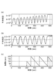
- FIG. 2 is a graph schematically showing the measurement principle of the change over time of the film thickness of the measurement object.
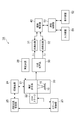
- FIG. 3 is a block diagram showing a configuration of an embodiment of the film thickness measuring apparatus.
- FIG. 4 is a diagram illustrating an example of the configuration of the measurement optical system.
- FIG. 5 is a diagram illustrating an example of the configuration of the measurement optical system.
- FIG. 6 is a diagram illustrating an example of the configuration of the spectroscopic optical system.
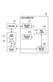
- FIG. 7 is a block diagram illustrating an example of the configuration of the film thickness analysis unit.
- FIG. 8 is a block diagram illustrating an example of the configuration of the measurement position setting unit.
- FIG. 1 is a diagram schematically showing a method for measuring a film thickness of a measurement object.
- FIG. 2 is a graph schematically showing the measurement principle of the change over time of the film thickness of the measurement object.
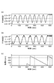
- FIG. 9 is a graph showing a first measurement example of film thickness measurement.
- FIG. 10 is a graph showing a second measurement example of film thickness measurement.
- FIG. 11 is a graph showing a third measurement example of film thickness measurement.
- FIG. 12 is a graph showing an example of a film thickness measuring method with wavelength switching.
- FIG. 13 is a graph illustrating a specific example of analysis processing for film thickness measurement.
- FIG. 14 is a graph illustrating a specific example of analysis processing for film thickness measurement.
- FIG. 15 is a graph illustrating a specific example of analysis processing for film thickness measurement.
- FIG. 16 is a graph illustrating a specific example of analysis processing for film thickness measurement.
- FIG. 17 is a graph illustrating a specific example of analysis processing for film thickness measurement.
- FIG. 18 is a graph illustrating a specific example of analysis processing for film thickness measurement.
- FIG. 1 is a diagram schematically showing a method for measuring a film thickness of a measurement object.
- FIG. 2 is a graph schematically showing the measurement principle of the time change of the film thickness of the measurement object.
- This film thickness measurement method measures the time change of the absolute value of the film thickness for a film-like measurement object having a first surface and a second surface.
- the first surface of the measurement object will be described as the upper surface on which the measurement light is incident, and the second surface will be described as the lower surface on the opposite side.
- a semiconductor film 15 formed on the substrate 12 is shown as an example of a film-like measurement object.
- an etching process is considered for such a semiconductor film 15. In the etching process, the film thickness d of the semiconductor film 15 decreases with time as the process proceeds.
- the film thickness measurement d is measured from the upper surface (first surface) 16 side of the semiconductor film 15 opposite to the substrate 12 with respect to the sample 10 including the substrate 12 and the semiconductor film 15.
- Measuring light L0 is supplied.
- interference light generated by interference between the reflected light L1 from the upper surface 16 and the reflected light L2 from the lower surface (second surface, the boundary surface between the substrate 12 and the semiconductor film 15) 17 is detected.
- the film thickness d of the semiconductor film 15 is measured.
- FIG. 1 for easy viewing, the optical path of the measurement light L0 irradiated on the semiconductor film 15 and the optical paths of the reflected lights L1 and L2 from the upper surface 16 and the lower surface 17 of the semiconductor film 15 are respectively shown. The position is shifted.
- the first measurement light component having the first wavelength ⁇ 1 and the second measurement light component having the second wavelength ⁇ 2 different from the first wavelength are applied to the sample 10 including the semiconductor film 15.
- the interference light of the reflected light L1 and L2 from the upper surface 16 and the lower surface 17 of the measurement light L0 is decomposed according to the wavelength, and the first interference light component having the wavelength ⁇ 1 and the second interference light component having the wavelength ⁇ 2 are obtained.
- the detection is performed separately (spectral step), the intensity of each of the first and second interference light components at each time point is detected, and the change of the interference intensity with time is acquired (detection step).
- the time change of the film thickness d of the semiconductor film 15 is obtained with reference to the time change of the detected intensity of the first and second interference light components (film thickness analysis step).
- the intensity I (t of the interference light generated by the interference of the reflected lights L1 and L2 ) Is expressed by the following formula (1) by the optical path length difference 2nd generated between the reflected lights L1 and L2. Shows the change over time. That is, when the measurement light L0 having the wavelength ⁇ is used, the interference intensity I (t) of the obtained reflected light changes in a cosine wave with the time change of the film thickness d due to the etching process or the like.
- A is the amplitude of fluctuation of the interference intensity
- B is an offset.
- FIG. Graph of FIG. 2 (a) shows temporal change in detected intensity I (t) of the first first interference light component of the wavelength lambda 1.
- the phase ⁇ 1 at each time point of the interference intensity I is expressed as follows. It becomes.
- n 1 is the refractive index of the semiconductor film 15 at the wavelength ⁇ 1 .
- the graph of FIG. 2 (b) shows the detection time change in the intensity I (t) of the second interference light component of the second wavelength lambda 2.
- the phase ⁇ 2 at each time point of this interference intensity I is similarly It becomes.
- n 2 is the refractive index of the semiconductor film 15 at the wavelength ⁇ 2 .
- the semiconductor film 15 supplies the measurement light L0 including the light components of the wavelengths ⁇ 1 and ⁇ 2 .
- the phases ⁇ 1 and ⁇ 2 and the periods ⁇ t 1 and ⁇ t 2 in the time change of the detection intensity of the first and second interference light components are different from each other in the wavelengths ⁇ 1 and ⁇ 2 .
- the phase and period differ with respect to the change in the film thickness d.
- these time-varying phases ⁇ 1 and ⁇ 2 of the interference intensity perform, for example, FFT (Fast Fourier Transform) analysis on data in a predetermined range (preferably a range of two cycles or more) of the interference intensity I. Can be obtained.
- FFT Fast Fourier Transform
- the wavelength lambda 1, the first lambda 2, the phase phi 1 of each of the second interference light component, for phi 2, when obtaining the phase difference between the two wavelengths, the phase difference [Delta] [phi 12 is the following formula (4) It becomes. That is, the phase difference ⁇ 12 between the first phase ⁇ 1 and the second phase ⁇ 2 changes in proportion to the film thickness d of the measurement object. Accordingly, as shown in the graph of FIG. 2 (c), the first, the change in the phase difference [Delta] [phi 12 with time variation of the detected intensity of the second interference light component, the absolute value of the film thickness d of the semiconductor layer 15, and The time change can be obtained with high accuracy.
- the end point detection and process control based on the end point detection can be performed with high accuracy.
- the relationship between the target film thickness D and the corresponding target phase difference ⁇ is expressed by the following equation: (5.1), (5.2) Represented by Therefore, using such a relationship, for example, a method in which the time when it is determined that the film thickness d of the semiconductor film 15 has decreased to the desired film thickness D from the measured phase difference ⁇ is set as the end point of the etching process.
- the end point of the etching process can be detected.
- Such process control can be similarly executed in, for example, control of thin film formation processing in which the film thickness d of the semiconductor film 15 increases with time.
- the absolute value of the film thickness d can be measured by the above-described method because the phase difference ⁇ 12 varies within the range of 0 to 2 ⁇ . (Interval ⁇ t 12 in graph (c)). For this reason, the maximum value d max of the film thickness at which the absolute value can be measured in the above method is expressed by the following formula (6). It becomes.
- the film thickness d is first measured by another method, and when the film thickness d falls within a range in which the absolute value can be measured. Therefore, it is preferable to switch to the film thickness measurement by the above method.
- Examples of such other film thickness measurement methods include a method of measuring a relative film thickness change from a film thickness given as an initial value. In this case, the reflected interference light is detected for the measurement light of one wavelength, the change rate of the film thickness (for example, the etching rate) is obtained from the time change of the intensity, and the film thickness change amount is subtracted from the initial value of the film thickness.
- a method for obtaining the film thickness can be used.
- FIG. 3 is a block diagram showing a configuration of an embodiment of the film thickness measuring apparatus.
- the semiconductor film 15 (see FIG. 1) of the sample 10 installed in the processing chamber of the semiconductor processing apparatus (for example, etching apparatus) 20 is the measurement object.
- the film thickness measurement apparatus 1A includes a measurement optical system 21, a measurement light source 28, a spectroscopic optical system 30, photodetectors 31 and 32, and a film thickness analysis unit 40.
- a measurement light source 28 that supplies measurement light L0 to the semiconductor film 15 of the sample 10 in the processing apparatus 20 via the measurement optical system 21 is provided.
- the measurement light source 28 uses the measurement light L0 including at least the measurement light component of the first wavelength ⁇ 1 and the measurement light component of the second wavelength ⁇ 2 as the semiconductor film of the measurement object. 15 is supplied.
- a white light source that supplies white light in a wavelength region including the first wavelength ⁇ 1 and the second wavelength ⁇ 2 as the measurement light L 0 can be suitably used.
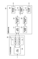
- FIG.4 and FIG.5 is a figure which shows an example of a structure of the measurement optical system 21 in 1 A of film thickness measuring apparatuses.
- the measurement light input fiber 281 that guides the measurement light from the measurement light source 28 to the measurement optical system 21 including the objective lens 211 disposed to face the sample 10, the time of acquiring the image of the sample 10, etc.
- An illumination light input fiber 282 that guides the illumination light used for and a reflected light output fiber 308 that guides the reflected light from the sample 10 to the spectroscopic optical system 30 are connected.
- the measurement light L 0 from the measurement light source 28 is input to the measurement optical system 21 by the input fiber 281, passes through the half mirror 212, and is reflected by the reflection mirror 213. And supplied to the semiconductor film 15 of the sample 10 through the objective lens 211.
- the reflected lights L 1 and L 2 from the upper and lower surfaces of the semiconductor film 15 are reflected by the reflecting mirror 213, the half mirror 212, and the reflecting mirror 214, and the spectroscopic optics through the output fiber 308. It is output to the system 30.
- the spectroscopic optical system 30 is spectroscopic means for spectroscopically reflecting reflected light input from the sample 10 via the measurement optical system 21.
- the spectroscopic optical system 30 is the first of the interference lights of the interference light generated by interference between the reflected light L1 from the upper surface of the semiconductor film 15 and the reflected light L2 from the lower surface of the semiconductor film 15.
- the first interference light component having the wavelength ⁇ 1 caused by the one measurement light component and the second interference light component having the wavelength ⁇ 2 caused by the second measurement light component are separately decomposed so as to be detected.
- FIG. 6 is a diagram illustrating an example of the configuration of the spectroscopic optical system 30.
- the spectroscopic optical system 30 includes an incident slit 301, a collimating optical system 302, a diffraction grating 303 as a dispersive element, and a focusing optical system 304.
- the interference light decomposed into the interference light components of each wavelength by the diffraction grating 303 forms an image on the wavelength spectrum output surface 305 via the focusing optical system 304 and is disposed on the output surface 305.
- Each wavelength component is detected by a detector.
- Photodetectors 31 and 32 are provided as detection means for detecting.
- the first photodetector 31 detects the first interference light component having the wavelength ⁇ 1 and outputs a detection signal indicating the intensity thereof.
- the second photodetector 32 detects the second interference light component having the wavelength ⁇ 2 and outputs a detection signal indicating the intensity thereof.
- Such a detecting means is arranged on the output surface 305 of the spectroscopic optical system 30 shown in FIG. 6, for example, and detects a plurality of light detection components that detect the intensity of each interference light component decomposed by the spectroscopic optical system 30. It can be constituted by a multi-channel photodetector in which elements are arranged. In this case, among the plurality of light detection elements of the light detector, one or a plurality of light detection elements that detect the first interference light component having the wavelength ⁇ 1 function as the first light detector 31. Similarly, one or more photodetectors that detect the second interference light component having the wavelength ⁇ 2 function as the second photodetector 32.
- the film thickness analysis unit 40 includes the first phase ⁇ 1 in the temporal change in the detection intensity of the first interference light component and the second phase ⁇ in the temporal change in the detection intensity of the second interference light component.
- 2 is a film thickness analysis means for obtaining a phase difference ⁇ 12 with respect to 2 and obtaining a time change of the film thickness d of the semiconductor film 15 as a measurement object based on the phase difference.
- FIG. 7 is a block diagram illustrating an example of the configuration of the film thickness analysis unit 40.
- the film thickness analysis unit 40 includes a phase analysis unit 41, a measurement phase difference acquisition unit 42, a phase difference information processing unit 45, and a film thickness information output unit 46.
- the spectroscopic means and the detection means are configured as a spectroscopic measurement device 35 having a spectroscopic optical system 30 and a multichannel photodetector 33 including first and second photodetectors 31 and 32.
- the phase analysis unit 41 receives the detection signal from the spectroscopic measurement device 35, and uses the first phase ⁇ 1 in the interference light component detected by the photodetector 31 and the interference light component detected by the photodetector 32.
- the second phase ⁇ 2 is calculated.
- the measurement phase difference acquisition unit 42 calculates the phase difference ⁇ 12 for the phases ⁇ 1 and ⁇ 2 of the first and second interference light components calculated by the phase analysis unit 41.
- the phase difference information processing unit 45 performs predetermined data processing on the phase difference ⁇ 12 acquired by the measurement phase difference acquisition unit 42, and based on the phase difference ⁇ 12 , the film thickness d of the semiconductor film 15 to be measured. Necessary information on the absolute value of, and its time change is derived.
- the phase difference information processing unit 45 calculates the absolute value of the film thickness d as the film thickness information from the measured phase difference ⁇ 12 based on the relational expression shown in Expression (4).
- processor 45 may information itself of the phase difference [Delta] [phi 12 that is not converted into a film thickness of d as the thickness information indicating a thickness d.
- the film thickness information output unit 46 outputs information about the film thickness d of the semiconductor film 15 obtained by the phase difference information processing unit 45.
- the film thickness analysis unit 40 shown in FIG. 7 shows a configuration in which the end point of the etching process is detected by assuming a time change in which the film thickness d of the semiconductor film 15 decreases due to the etching process.
- the film thickness analysis unit 40 of the present configuration example further includes a reference film thickness storage unit 43, a reference phase difference acquisition unit 44, and an end point information output unit 47.
- the reference film thickness storage unit 43 stores in advance a reference film thickness (target film thickness) D indicating the value of the film thickness d of the semiconductor film 15 to be the end point of the etching process.
- the reference phase difference acquisition unit 44 calculates a reference phase difference (target phase difference) ⁇ corresponding to the reference film thickness D read from the storage unit 43 as shown in the equation (5.1).
- the phase difference information processing unit 45 compares the measurement phase difference ⁇ 12 acquired by the measurement phase difference acquisition unit 42 with the reference phase difference ⁇ acquired by the reference phase difference acquisition unit 44.
- the processing unit 45 determines whether or not the etching process has reached the end point, for example, based on whether or not the measurement phase difference ⁇ 12 and the reference phase difference ⁇ match, and is determined to have reached the end point. Then, an end point detection signal for stopping the etching process is output via the end point information output unit 47.
- a film thickness analysis part 40 can be comprised by the computer with which the predetermined
- a measurement control unit 50 refers to the film thickness information from the film thickness information output unit 46 of the film thickness analysis unit 40 or the end point information from the end point information output unit 47, and sets each unit of the measuring apparatus 1A and the processing apparatus 20 as follows. By controlling, the film thickness measurement operation in the measurement apparatus 1A and the operation such as the etching process in the processing apparatus 20 are performed.
- an input device 51 and a display device 52 are connected to the measurement control unit 50.
- the input device 51 is used to input information, conditions, instructions, and the like necessary for the measurement operation in the measurement device 1 ⁇ / b> A and the processing operation in the processing device 20.
- the input device 51 is used to input, for example, measurement wavelengths ⁇ 1 and ⁇ 2 used in the film thickness analysis unit 40, refractive indexes n 1 and n 2 of the measurement object at each wavelength, a target film thickness D for the etching process, and the like. Can be used. Further, the film thickness value at the start of the process may be further input. However, these conditions and numerical values may be prepared in advance in the film thickness analysis unit 40.
- the display device 52 is used to display necessary information about the above-described measurement operation and processing operation to the operator.
- an XY ⁇ stage 22 is provided for the measurement optical system 21.
- the XY ⁇ stage 22 adjusts the position, angle, etc. of the measurement optical system 21 in the X direction, Y direction, and ⁇ direction, so that the measurement position and measurement of the film thickness d in the semiconductor film 15 by the film thickness measuring apparatus 1A. Used to adjust conditions.
- the XY ⁇ stage 22 is driven and controlled by a stage control unit 23.
- an imaging device 24 and a measurement position setting unit 25 are further provided for the sample 10 and the measurement optical system 21 in the processing device 20.
- the imaging device 24 is a position confirmation imaging device for confirming the measurement position of the film thickness d on the semiconductor film 15 by the measuring device 1A.
- the measurement position setting unit 25 refers to the image of the sample 10 including the semiconductor film 15 acquired by the imaging device 24 via the measurement optical system 21 and sets the film thickness measurement position for the sample 10.
- FIG. 8 is a block diagram illustrating an example of the configuration of the measurement position setting unit 25.
- the measurement position setting unit 25 includes a measurement image recognition unit 251, a reference image storage unit 252, an image comparison unit 253, and a control condition calculation unit 254.
- the measurement image recognition unit 251 receives the image data of the sample 10 acquired by the imaging device 24, and performs pattern recognition of the measurement pattern in the image.
- the reference image storage unit 252 stores in advance a reference image for specifying a position to be set as a measurement position of the film thickness d in the semiconductor film 15.
- the image comparison unit 253 compares the measurement pattern in the measurement image recognized by the recognition unit 251 with the reference pattern in the reference image stored in the storage unit 252 by a method such as calculation of a difference image. Further, the control condition calculation unit 254 calculates the necessity of adjustment of the measurement position and the control condition when adjustment is necessary based on the comparison result between the measurement image and the reference image in the image comparison unit 253. . Then, the XY ⁇ stage 22 and the measurement optical system 21 are driven and controlled via the stage control unit 23 based on the control condition obtained by the calculation unit 254, so that the film thickness d of the sample 10 with respect to the semiconductor film 15 is increased. Measurement position and measurement conditions are set and controlled.
- the measurement position of the film thickness d of the sample 10 with respect to the semiconductor film 15 is the position of the teg on the semiconductor wafer. This is because if the position on the semiconductor chip is set as the measurement position, the film thickness d may not be accurately measured due to a step difference such as a mask.
- the first and second wavelengths ⁇ 1 and ⁇ 2 are applied to the semiconductor film 15 on the substrate 12 which is a film-like measurement object.
- the measurement light L0 including the light component is supplied, and the interference light of the reflected light L1 and L2 from the upper surface 16 and the lower surface 17 is spectrally detected by the spectroscopic optical system 30 and the photodetectors 31 and 32.
- the time change of the film thickness d of the semiconductor film 15 is obtained. According to such a configuration, it is possible to accurately measure the absolute value of the film thickness d of the measurement object and its temporal change by the phase difference of the time waveform of the detected intensity between the two wavelengths.
- the measurement target is the semiconductor film 15 on the substrate 12, and the time change of the film thickness d of the semiconductor film 15 during the execution of a predetermined process is measured. It is preferable to do. With such a configuration, process control such as processing end point detection can be accurately performed during execution of a semiconductor process such as an etching process or a thin film forming process in which the film thickness d of the semiconductor film 15 decreases or increases.
- the above method is generally applicable to the measurement of the film thickness d of a film-like measurement object.
- the measurement light source 28 is a white light source that supplies white light in a wavelength region including the first and second wavelengths ⁇ 1 and ⁇ 2 as the measurement light L0.
- the measurement light L0 including at least the measurement light components of the first and second wavelengths ⁇ 1 and ⁇ 2 can be suitably supplied.
- the spectroscopic unit divides the interference light into the interference light of each wavelength with respect to the configuration of the spectroscopic unit that splits the interference light of the reflected light L1 and L2 from the sample 10 and the detection unit that detects the interference light.
- the detection means has a multi-channel photodetector in which a plurality of photodetectors for detecting the intensity of each interference light component decomposed by the spectroscopy optical system 30 are arranged. A configuration can be used.
- the measurement light source may have a configuration capable of supplying the measurement light L0 including at least the measurement light components of the first and second wavelengths ⁇ 1 and ⁇ 2 .
- Examples of such a measurement light source include a light source capable of supplying a plurality of monochromatic lights simultaneously, such as a configuration in which a plurality of semiconductor lasers or LEDs are combined.
- a wavelength selection filter such as a band pass filter can be used as the spectroscopic means.
- a detection means photodetectors, such as a photodiode installed in combination with the wavelength selection filter, can be used, for example.
- the first wavelength selection filter and the first photodetector corresponding to the first wavelength ⁇ 1 , and the second wavelength selection filter and the second photodetector corresponding to the second wavelength ⁇ 2 , the spectroscopic means and Detection means can be configured.
- FIG. 9 is a graph showing a first measurement example of film thickness measurement by the measurement method described above.
- a graph (a) shows a temporal change in the detection intensity I of the interference light component of the first wavelength ⁇ 1
- time indicates a change
- the graph (c) shows a temporal change in the film thickness d of the measuring object corresponding to the phase difference [Delta] [phi 12.
- the absolute value of the film thickness d of the semiconductor film 15 as the measurement object and the time change thereof are accurately determined by the phase difference of the time change of the detection intensity of the first and second interference light components. Can be sought.
- the end point of the etching process is detected by setting the target film thickness D as a threshold value with respect to the time change of the absolute value of the measured film thickness d. be able to.
- the range in which the absolute value of the film thickness d of the measurement object can be measured is during the phase difference is changing within the range of 0 to 2 ⁇ .
- the maximum value d max of the film thickness whose absolute value can be measured is Is required. That is, in this measurement example, if the film thickness d of the measurement object is 264.99 nm or less, the absolute value of the film thickness d can be measured by the above method.
- FIG. 10 is a graph showing a second measurement example of film thickness measurement by the above-described method, where graph (a) shows the change over time of detection intensity I of the first interference light component, and graph (b) The time change of the detection intensity I of the second interference light component is shown, and the graph (c) shows the time change of the film thickness d of the measurement object.
- the wavelength interval is 190 nm.
- FIG. 11 is a graph showing a third measurement example of film thickness measurement by the above method, where graph (a) shows the change over time of detection intensity I of the first interference light component, and graph (b) The time change of the detection intensity I of the second interference light component is shown, and the graph (c) shows the time change of the film thickness d of the measurement object.
- the wavelength interval is 195 nm.
- the correspondence between the phase difference ⁇ 12 measured by the measuring apparatus 1A and the film thickness d, the measurable film thickness range, and the measurement accuracy are the wavelength ⁇ 1 , changes depending on the ⁇ 2 of the set. Therefore, it is possible to set or change the measurement conditions of the film thickness d by setting and changing the wavelengths ⁇ 1 and ⁇ 2 used for film thickness measurement.
- the measurement light source 28 is configured to be able to supply three or more measurement light components having different wavelengths as components of the measurement light L0.
- the spectroscopic means and the detection means using the spectroscopic optical system 30 and the photodetectors 31 and 32 are configured so that the wavelengths ⁇ 1 and ⁇ 2 used for measurement can be changed.
- the measurement conditions can be suitably set and changed in accordance with the time change state of the film thickness d of the measurement object.
- a white light source or a light source combining three or more types of monochromatic light sources can be used.
- a configuration in which a spectroscopic optical system (spectrometer) and a multichannel photodetector are combined can be used as the spectroscopic unit and the detection unit.
- the first and second wavelength intervals ⁇ are gradually increased with time. It is preferable to change the second wavelengths ⁇ 1 and ⁇ 2 .
- the maximum value d max of the film thickness at which the absolute value can be measured is Is required.
- the measurable film thickness range is widened.
- the resolution of film thickness measurement and the measurement accuracy decrease.
- the wavelength interval ⁇ between the wavelengths ⁇ 1 and ⁇ 2 is widened, the measurable film thickness range becomes narrow, but the resolution and measurement accuracy of the film thickness measurement are improved. Therefore, in measuring the film thickness d, it is preferable to switch the wavelengths ⁇ 1 and ⁇ 2 as necessary in consideration of the relationship between the wavelength interval ⁇ , the measurement range, and the measurement accuracy.
- FIG. 12 is a graph showing an example of a film thickness measuring method with wavelength switching.
- Figure 12 (a) shows the time variation of the graph C1 retardation [Delta] [phi 12 in this case, the measurable thickness range is 2000 nm.
- FIG. 12B shows a graph C2 of the time change of the phase difference at this time, and the measurable film thickness range is 1000 nm.
- FIG. 12C shows a graph C3 of the time change of the phase difference at this time, and the measurable film thickness range is 500 nm.
- FIG. 12 (d) shows an example of a film thickness measurement method with wavelength switching when using these first to third measurement conditions.
- the measurement condition switching threshold value ⁇ T is set with respect to the decrease in the film thickness d of the semiconductor film 15 by the etching process, and the measurement condition is switched when the phase difference ⁇ 12 decreases to this threshold value. That is, the first measurement condition (C1) having the widest measurement range is applied in the measurement section T1 including the time when the measurement of the film thickness d is started.
- the film thickness d of the semiconductor film 15 can be measured with particularly high accuracy by switching the wavelength interval ⁇ of the two wavelengths so as to gradually increase as the film thickness decreases as the etching process proceeds. It becomes. In the example described above, but by changing the wavelength interval by changing the wavelength lambda 2 by fixing the wavelength lambda 1, it may be changed wavelength lambda 1 by fixing the wavelength lambda 2. Alternatively, both the wavelengths ⁇ 1 and ⁇ 2 may be changed.
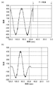
- 13 to 18 are graphs for explaining specific examples of analysis processing for measuring the film thickness of the measurement object. Note that, here, a method for calculating a phase in the time change of the detection intensity of the reflected interference light is described for the measurement light of one wavelength ⁇ , but the same applies to the measurement using the two wavelengths ⁇ 1 and ⁇ 2 . It is possible to analyze by the method.
- the analysis interval T used for the phase analysis (for example, the number of data used for the phase analysis) is obtained with respect to the temporal change data of the detection intensity of the reflected interference light acquired for the light of the wavelength ⁇ . ) Is set. Further, as shown in the graph (b) of FIG. 13 and the graph (a) of FIG. 14, the measurement data of the segment T thus cut out is in a direction opposite to the time axis direction starting from the current time point. Consider the traveling wave and change its axis.
- the offset is adjusted so that the average intensity becomes 0, the 0th-order component having a large signal intensity is removed from the detected intensity data, and the oscillation is centered on 0. Change with time. Furthermore, as shown in the graph (a) of FIG. 15, the analysis interval is extended in order to increase the frequency resolution in the FFT analysis. At this time, it is preferable to set the detection intensity to 0 for the data extension portion in the analysis data of the detection intensity. Subsequently, as shown in the graph (b) of FIG. 15, a window function is applied to the analysis data of the detected intensity. This is for removing a pseudo frequency signal generated due to a finite data length. As the window function in this case, specifically, for example, a Hamming window can be used. Alternatively, other window functions such as a Gaussian window may be used.
- phase ⁇ 0.
- the phase here refers to the amount of delayed phase with respect to a cosine wave with the current time as the origin when considering a wave traveling in a direction opposite to the time axis direction as described above.
- the value of the phase can be obtained from the real part and the imaginary part of the intensity obtained by the Fourier transform by using antan (imaginary part / real part).
- FIGS. 17 and 18 show analysis examples when the time change of the detection intensity has passed a quarter cycle.
- the analysis interval T used for the phase analysis is set for the data of the temporal change in the detection intensity of the reflected interference light.
- the result obtained by finally performing Fourier transform is shown in the graph of FIG.
- phase analysis is performed for each of the interference light components of the first and second wavelengths ⁇ 1 and ⁇ 2 , and the absolute value of the film thickness d of the measurement object is determined based on the phase difference.
- find the time change of the value for example, a film thickness change rate such as an etching rate can be obtained.
- process control such as detection of the end point of the etching process, the reference film thickness D set in advance and the film thickness d measured, or the corresponding reference phase difference ⁇ and the measured phase difference ⁇ 12
- the process control can be performed by a method such as outputting a process end signal when both values match.
- FIG. 3 shows an example of the configuration of the measurement light source, the spectroscopic unit, and the detection unit used for film thickness measurement. Specifically, various configurations other than the above can be used. It is. Further, the specific phase calculation method and the film thickness analysis method for obtaining the film thickness d from the detected detection intensity of the reflected interference light are not limited to the above-described analysis examples. Various methods may be used.
- the film thickness measurement apparatus is a film thickness measurement apparatus that measures the change over time of the film thickness of a film-like measurement object having a first surface and a second surface, and (1) has a first wavelength.
- the interference light in which the reflected light from the first surface and the reflected light from the second surface interfere, the first interference light component of the first wavelength and the second interference light component of the second wavelength are decomposed so that they can be detected separately.
- Spectroscopic means for performing (3) detection means for detecting the intensity of each of the first interference light component and the second interference light component at each time point, and (4) in the time change of the detection intensity of the first interference light component.
- Phase between the first phase and the second phase in the temporal change in the detection intensity of the second interference light component Based on uses a configuration and a film thickness analyzer means for determining the temporal change in the film thickness of the measuring object.
- the film thickness measurement method is a film thickness measurement method for measuring a time change of the film thickness of a film-like measurement object having a first surface and a second surface, and (1) First A measurement light supply step for supplying measurement light including at least a first measurement light component having a wavelength and a second measurement light component having a second wavelength different from the first wavelength from the measurement light source to the measurement object; ) About the interference light which the reflected light from the 1st surface of the measuring object of measurement light interfered with the reflected light from the 2nd surface, the 1st interference light component of the 1st wavelength, and the 2nd interference light of the 2nd wavelength A spectroscopic step for separately detecting components separately, (3) a detecting step for detecting the intensity of each of the first interference light component and the second interference light component at each time point, and (4) first interference light. Detection of first phase and second interference light component in time variation of component detection intensity Based on the phase difference between the second phase in the time variation of the degree, and using the configuration and
- the measurement object is a semiconductor film on a substrate, and the change in the film thickness over time during execution of a predetermined process is measured. It is preferable to do.
- the time change of the absolute value of the film thickness is measured to perform process control such as detection of the end point of the process. It can be performed with high accuracy.
- the measuring device is configured such that the measurement light source can supply three or more measurement light components having different wavelengths as the measurement light component, and the spectroscopic means and the detection means are used for measuring the temporal change of the film thickness.
- the first wavelength and the second wavelength may be configured to be changeable.
- the measurement method is configured such that the measurement light source can supply three or more measurement light components having different wavelengths as the measurement light component, and is used for measuring the temporal change in film thickness in the spectroscopic step and the detection step. It is good also as changing the 1st wavelength and 2nd wavelength to be performed. Thereby, according to the state of the time change of a film thickness, the measurement conditions can be set and changed suitably.
- the wavelength interval of 2 wavelengths may be expanded in steps. It is preferable to change the wavelength and the second wavelength. As an example of such a measurement, there is a measurement of a time change of the film thickness of the semiconductor film on the substrate during the execution of the etching process.
- the measurement light source is a white light source that supplies white light in a wavelength region including the first wavelength and the second wavelength as measurement light
- the spectroscopic means has a spectroscopic optical system that decomposes the interference light into interference light components of each wavelength
- the detection means detects a plurality of light that detects the intensity of each interference light component decomposed by the spectroscopic optical system.
- a configuration having a multi-channel photodetector in which elements are arranged can be used.
- various configurations can be used for the measurement light source, the spectroscopic unit, and the detection unit.
- the present invention can be used as a film thickness measuring apparatus and a film thickness measuring method capable of accurately measuring a temporal change in the film thickness of a film-like measurement object.
- SYMBOLS 1A Film thickness measuring apparatus, 10 ... Sample, 12 ... Substrate, 15 ... Semiconductor film (measuring object), 16 ... Upper surface (first surface), 17 ... Lower surface (second surface), 20 ... Processing device, 21 ... Measurement optical system, 22 ... XY ⁇ stage, 23 ... Stage controller, 24 ... Imaging device, 25 ... Measurement position setting unit, 28 ... Measurement light source, 30 ... Spectroscopic optical system, 31 ... First photodetector, 32 ... Second Photo detector 33 ... Multi-channel photodetector 35 ... Spectral measurement device 40 ... Film thickness analysis unit 41 ... Phase analysis unit 42 ... Measurement phase difference acquisition unit 43 ...
- Reference film thickness storage unit 44 ... Reference A phase difference acquisition unit, 45 ... a phase difference information processing unit, 46 ... a film thickness information output unit, 47 ... an end point information output unit, 50 ... a measurement control unit, 51 ... an input device, 52 ... a display device.
Landscapes
- Physics & Mathematics (AREA)
- General Physics & Mathematics (AREA)
- Length Measuring Devices By Optical Means (AREA)
- Testing Or Measuring Of Semiconductors Or The Like (AREA)
Abstract
Description







Claims (10)
- 第1面及び第2面を有する膜状の測定対象物の膜厚の時間変化を測定する膜厚測定装置であって、
第1波長を有する第1測定光成分、及び前記第1波長とは異なる第2波長を有する第2測定光成分を少なくとも含む測定光を前記測定対象物へと供給する測定光源と、
前記測定光の前記測定対象物の前記第1面からの反射光、及び前記第2面からの反射光が干渉した干渉光について、前記第1波長の第1干渉光成分、及び前記第2波長の第2干渉光成分に分解する分光手段と、
前記第1干渉光成分、及び前記第2干渉光成分のそれぞれの各時点での強度を検出する検出手段と、
前記第1干渉光成分の検出強度の時間変化における第1位相と、前記第2干渉光成分の検出強度の時間変化における第2位相との位相差に基づいて、前記測定対象物の膜厚の時間変化を求める膜厚解析手段と
を備えることを特徴とする膜厚測定装置。 - 前記測定対象物は基板上の半導体膜であり、所定の処理の実行中における前記半導体膜の膜厚の時間変化を測定することを特徴とする請求項1記載の膜厚測定装置。
- 前記測定光源は、前記測定光の成分として互いに波長が異なる3成分以上の測定光成分を供給可能に構成され、前記分光手段及び前記検出手段は、膜厚の時間変化の測定に用いられる前記第1波長及び前記第2波長を変更可能に構成されていることを特徴とする請求項1または2記載の膜厚測定装置。
- 前記測定対象物について膜厚が減少する時間変化を測定する場合に、2波長の波長間隔を段階的に広げるように前記第1波長及び前記第2波長を変更することを特徴とする請求項3記載の膜厚測定装置。
- 前記測定光源は、前記第1波長及び前記第2波長を含む波長域の白色光を前記測定光として供給する白色光源であることを特徴とする請求項1~4のいずれか一項記載の膜厚測定装置。
- 前記分光手段は、前記干渉光を各波長の干渉光成分へと分解する分光光学系を有し、
前記検出手段は、前記分光光学系によって分解された各干渉光成分の強度を検出する複数の光検出素子が配列されたマルチチャンネル光検出器を有することを特徴とする請求項1~5のいずれか一項記載の膜厚測定装置。 - 第1面及び第2面を有する膜状の測定対象物の膜厚の時間変化を測定する膜厚測定方法であって、
第1波長を有する第1測定光成分、及び前記第1波長とは異なる第2波長を有する第2測定光成分を少なくとも含む測定光を測定光源から前記測定対象物へと供給する測定光供給ステップと、
前記測定光の前記測定対象物の前記第1面からの反射光、及び前記第2面からの反射光が干渉した干渉光について、前記第1波長の第1干渉光成分、及び前記第2波長の第2干渉光成分に分解する分光ステップと、
前記第1干渉光成分、及び前記第2干渉光成分のそれぞれの各時点での強度を検出する検出ステップと、
前記第1干渉光成分の検出強度の時間変化における第1位相と、前記第2干渉光成分の検出強度の時間変化における第2位相との位相差に基づいて、前記測定対象物の膜厚の時間変化を求める膜厚解析ステップと
を備えることを特徴とする膜厚測定方法。 - 前記測定対象物は基板上の半導体膜であり、所定の処理の実行中における前記半導体膜の膜厚の時間変化を測定することを特徴とする請求項7記載の膜厚測定方法。
- 前記測定光源は、前記測定光の成分として互いに波長が異なる3成分以上の測定光成分を供給可能に構成され、前記分光ステップ及び前記検出ステップにおいて、膜厚の時間変化の測定に用いられる前記第1波長及び前記第2波長を変更することを特徴とする請求項7または8記載の膜厚測定方法。
- 前記測定対象物について膜厚が減少する時間変化を測定する場合に、2波長の波長間隔を段階的に広げるように前記第1波長及び前記第2波長を変更することを特徴とする請求項9記載の膜厚測定方法。
Priority Applications (3)
| Application Number | Priority Date | Filing Date | Title |
|---|---|---|---|
| DE112010001378.0T DE112010001378B4 (de) | 2009-03-27 | 2010-01-20 | Filmdickenmessgerät und Messverfahren |
| CN2010800100495A CN102341670B (zh) | 2009-03-27 | 2010-01-20 | 膜厚测量装置以及测量方法 |
| US13/201,976 US8649023B2 (en) | 2009-03-27 | 2010-01-20 | Film thickness measurement device and measurement method |
Applications Claiming Priority (2)
| Application Number | Priority Date | Filing Date | Title |
|---|---|---|---|
| JP2009-078772 | 2009-03-27 | ||
| JP2009078772A JP5410806B2 (ja) | 2009-03-27 | 2009-03-27 | 膜厚測定装置及び測定方法 |
Publications (1)
| Publication Number | Publication Date |
|---|---|
| WO2010109933A1 true WO2010109933A1 (ja) | 2010-09-30 |
Family
ID=42780630
Family Applications (1)
| Application Number | Title | Priority Date | Filing Date |
|---|---|---|---|
| PCT/JP2010/050634 Ceased WO2010109933A1 (ja) | 2009-03-27 | 2010-01-20 | 膜厚測定装置及び測定方法 |
Country Status (7)
| Country | Link |
|---|---|
| US (1) | US8649023B2 (ja) |
| JP (1) | JP5410806B2 (ja) |
| KR (1) | KR101614977B1 (ja) |
| CN (1) | CN102341670B (ja) |
| DE (1) | DE112010001378B4 (ja) |
| TW (1) | TWI465682B (ja) |
| WO (1) | WO2010109933A1 (ja) |
Cited By (3)
| Publication number | Priority date | Publication date | Assignee | Title |
|---|---|---|---|---|
| CN102538688A (zh) * | 2011-12-26 | 2012-07-04 | 哈尔滨工业大学 | 红外宽波段透射式塑料薄膜厚度测量装置及测量方法 |
| CN102980530A (zh) * | 2012-12-05 | 2013-03-20 | 清华大学 | 一种基于空间光调制器的椭偏测量装置及测量方法 |
| WO2023084952A1 (ja) * | 2021-11-10 | 2023-05-19 | 株式会社コベルコ科研 | ウェハ厚さ測定装置および該方法 |
Families Citing this family (22)
| Publication number | Priority date | Publication date | Assignee | Title |
|---|---|---|---|---|
| JP5410806B2 (ja) | 2009-03-27 | 2014-02-05 | 浜松ホトニクス株式会社 | 膜厚測定装置及び測定方法 |
| WO2011045967A1 (ja) * | 2009-10-13 | 2011-04-21 | 浜松ホトニクス株式会社 | 膜厚測定装置および膜厚測定方法 |
| JP2012063321A (ja) | 2010-09-17 | 2012-03-29 | Hamamatsu Photonics Kk | 反射率測定装置、反射率測定方法、膜厚測定装置及び膜厚測定方法 |
| JP5891006B2 (ja) * | 2011-11-01 | 2016-03-22 | 東京エレクトロン株式会社 | 光干渉システム、基板処理装置及び計測方法 |
| CN102778202B (zh) * | 2012-03-23 | 2016-01-27 | 北京京东方光电科技有限公司 | 一种膜厚测量装置及方法 |
| CN103424078B (zh) * | 2012-05-15 | 2016-03-23 | 无锡华润上华科技有限公司 | 膜厚仪 |
| JP5997578B2 (ja) * | 2012-10-19 | 2016-09-28 | 東レエンジニアリング株式会社 | クロストーク補正係数算出方法およびクロストーク補正係数算出機能を備えた透明膜の膜厚測定装置 |
| US20150022658A1 (en) * | 2013-07-16 | 2015-01-22 | University Of North Carolina At Charlotte | Noise reduction techniques, fractional bi-spectrum and fractional cross-correlation, and applications |
| CN104655028B (zh) * | 2013-11-22 | 2017-08-22 | 睿励科学仪器(上海)有限公司 | 用于半导体基片测量的聚焦系统与聚焦方法 |
| CN104034272B (zh) * | 2014-06-24 | 2016-08-24 | 山东大学 | 一种宽光谱光干涉法测量薄膜厚度的系统 |
| CN105975125A (zh) * | 2016-04-29 | 2016-09-28 | 宇龙计算机通信科技(深圳)有限公司 | 调节触摸屏参数的方法、装置及终端设备 |
| CN207058321U (zh) * | 2016-05-11 | 2018-03-02 | 凯斯科技股份有限公司 | 具有氧化物层的晶片的抛光系统 |
| JP6533770B2 (ja) * | 2016-11-10 | 2019-06-19 | 日東電工株式会社 | 基準器、分光干渉式計測装置、塗布装置、分光干渉式計測装置の計測精度保証方法、及び、塗布膜の製造方法。 |
| JP6800800B2 (ja) * | 2017-04-06 | 2020-12-16 | 株式会社ニューフレアテクノロジー | 成長速度測定装置および成長速度検出方法 |
| JP6285597B1 (ja) * | 2017-06-05 | 2018-02-28 | 大塚電子株式会社 | 光学測定装置および光学測定方法 |
| JP6550101B2 (ja) * | 2017-07-13 | 2019-07-24 | Jfeテクノリサーチ株式会社 | 膜厚測定方法及び膜厚測定装置 |
| CN107607051B (zh) * | 2017-10-26 | 2019-07-30 | 京东方科技集团股份有限公司 | 一种膜厚检测装置 |
| JP6487579B1 (ja) | 2018-01-09 | 2019-03-20 | 浜松ホトニクス株式会社 | 膜厚計測装置、膜厚計測方法、膜厚計測プログラム、及び膜厚計測プログラムを記録する記録媒体 |
| KR20220008803A (ko) * | 2019-05-15 | 2022-01-21 | 후지코시 기카이 고교 가부시키가이샤 | 비접촉식 웨이퍼 두께 측정 장치 |
| JP7160779B2 (ja) * | 2019-10-03 | 2022-10-25 | 信越半導体株式会社 | 薄膜付ウェーハの膜厚分布の測定方法 |
| DE102020115544B4 (de) * | 2020-06-11 | 2022-03-31 | Trioptics Gmbh | Messvorrichtung und Verfahren zum Messen einer Reflektivität von beschichteten optischen Elementen |
| CN112747682B (zh) * | 2020-12-22 | 2022-05-13 | 天津大学 | 一种基于光载微波干涉的液膜厚度测量系统 |
Citations (5)
| Publication number | Priority date | Publication date | Assignee | Title |
|---|---|---|---|---|
| JPS63122906A (ja) * | 1986-11-13 | 1988-05-26 | Toshiba Corp | 膜厚測定装置 |
| JPH06252113A (ja) * | 1993-02-26 | 1994-09-09 | Matsushita Electric Ind Co Ltd | 半導体基板の平坦化方法 |
| JPH1114312A (ja) * | 1997-06-24 | 1999-01-22 | Toshiba Corp | 成膜装置及びエッチング装置 |
| JPH11132726A (ja) * | 1997-10-24 | 1999-05-21 | Canon Inc | 膜厚測定方法 |
| JP2005084019A (ja) * | 2003-09-11 | 2005-03-31 | Akifumi Ito | 基板の温度測定方法 |
Family Cites Families (16)
| Publication number | Priority date | Publication date | Assignee | Title |
|---|---|---|---|---|
| US4293224A (en) * | 1978-12-04 | 1981-10-06 | International Business Machines Corporation | Optical system and technique for unambiguous film thickness monitoring |
| JPS6350703A (ja) | 1986-08-21 | 1988-03-03 | Chino Corp | 膜厚測定装置 |
| JPS6428509A (en) * | 1987-07-23 | 1989-01-31 | Nippon Kokan Kk | Apparatus for measuring thickness of film |
| EP0412728A3 (en) * | 1989-08-11 | 1991-04-10 | American Telephone And Telegraph Company | Interferometric method and apparatus for controlling film thickness |
| JP2612089B2 (ja) | 1990-08-10 | 1997-05-21 | 富士通株式会社 | 被エッチング膜の膜厚検出方法、膜厚検出装置及びエッチング装置 |
| JP2656869B2 (ja) | 1991-12-24 | 1997-09-24 | 沖電気工業株式会社 | ドライエッチングにおける終点検出方法 |
| JP3491337B2 (ja) * | 1994-05-13 | 2004-01-26 | 株式会社デンソー | 半導体厚非接触測定装置 |
| JP3402321B2 (ja) * | 2000-12-08 | 2003-05-06 | 株式会社ニコン | 測定装置、研磨状況モニタ装置、研磨装置、半導体デバイス製造方法、並びに半導体デバイス |
| US6888639B2 (en) | 2001-09-24 | 2005-05-03 | Applied Materials, Inc. | In-situ film thickness measurement using spectral interference at grazing incidence |
| US7306696B2 (en) * | 2002-11-01 | 2007-12-11 | Applied Materials, Inc. | Interferometric endpoint determination in a substrate etching process |
| EP1467177A1 (en) * | 2003-04-09 | 2004-10-13 | Mitsubishi Chemical Engineering Corporation | Method and apparatus for measuring thicknesses of layers of multilayer thin film |
| JP4216209B2 (ja) | 2004-03-04 | 2009-01-28 | 大日本スクリーン製造株式会社 | 膜厚測定方法および装置 |
| JP2007040930A (ja) * | 2005-08-05 | 2007-02-15 | Ebara Corp | 膜厚測定方法及び基板処理装置 |
| US7646489B2 (en) | 2007-04-25 | 2010-01-12 | Yokogawa Electric Corporation | Apparatus and method for measuring film thickness |
| CN100573036C (zh) | 2008-04-20 | 2009-12-23 | 华中科技大学 | 一种薄膜厚度和折射率的光学测量方法 |
| JP5410806B2 (ja) | 2009-03-27 | 2014-02-05 | 浜松ホトニクス株式会社 | 膜厚測定装置及び測定方法 |
-
2009
- 2009-03-27 JP JP2009078772A patent/JP5410806B2/ja active Active
-
2010
- 2010-01-20 DE DE112010001378.0T patent/DE112010001378B4/de active Active
- 2010-01-20 US US13/201,976 patent/US8649023B2/en not_active Expired - Fee Related
- 2010-01-20 WO PCT/JP2010/050634 patent/WO2010109933A1/ja not_active Ceased
- 2010-01-20 CN CN2010800100495A patent/CN102341670B/zh active Active
- 2010-01-20 KR KR1020117013694A patent/KR101614977B1/ko not_active Expired - Fee Related
- 2010-01-27 TW TW099102302A patent/TWI465682B/zh active
Patent Citations (5)
| Publication number | Priority date | Publication date | Assignee | Title |
|---|---|---|---|---|
| JPS63122906A (ja) * | 1986-11-13 | 1988-05-26 | Toshiba Corp | 膜厚測定装置 |
| JPH06252113A (ja) * | 1993-02-26 | 1994-09-09 | Matsushita Electric Ind Co Ltd | 半導体基板の平坦化方法 |
| JPH1114312A (ja) * | 1997-06-24 | 1999-01-22 | Toshiba Corp | 成膜装置及びエッチング装置 |
| JPH11132726A (ja) * | 1997-10-24 | 1999-05-21 | Canon Inc | 膜厚測定方法 |
| JP2005084019A (ja) * | 2003-09-11 | 2005-03-31 | Akifumi Ito | 基板の温度測定方法 |
Cited By (5)
| Publication number | Priority date | Publication date | Assignee | Title |
|---|---|---|---|---|
| CN102538688A (zh) * | 2011-12-26 | 2012-07-04 | 哈尔滨工业大学 | 红外宽波段透射式塑料薄膜厚度测量装置及测量方法 |
| CN102980530A (zh) * | 2012-12-05 | 2013-03-20 | 清华大学 | 一种基于空间光调制器的椭偏测量装置及测量方法 |
| WO2023084952A1 (ja) * | 2021-11-10 | 2023-05-19 | 株式会社コベルコ科研 | ウェハ厚さ測定装置および該方法 |
| JP2023070862A (ja) * | 2021-11-10 | 2023-05-22 | 株式会社コベルコ科研 | ウェハ厚さ測定装置および該方法 |
| JP7619928B2 (ja) | 2021-11-10 | 2025-01-22 | 株式会社コベルコ科研 | ウェハ厚さ測定装置および該方法 |
Also Published As
| Publication number | Publication date |
|---|---|
| US20110299097A1 (en) | 2011-12-08 |
| CN102341670A (zh) | 2012-02-01 |
| JP2010230515A (ja) | 2010-10-14 |
| TW201037266A (en) | 2010-10-16 |
| US8649023B2 (en) | 2014-02-11 |
| TWI465682B (zh) | 2014-12-21 |
| KR101614977B1 (ko) | 2016-04-22 |
| JP5410806B2 (ja) | 2014-02-05 |
| DE112010001378T8 (de) | 2012-08-16 |
| DE112010001378B4 (de) | 2025-05-15 |
| KR20120004394A (ko) | 2012-01-12 |
| DE112010001378T5 (de) | 2012-05-24 |
| CN102341670B (zh) | 2013-12-04 |
Similar Documents
| Publication | Publication Date | Title |
|---|---|---|
| JP5410806B2 (ja) | 膜厚測定装置及び測定方法 | |
| JP5519688B2 (ja) | 膜厚測定装置および膜厚測定方法 | |
| EP0875743B1 (en) | A wavemeter and an arrangement for the adjustment of the wavelength of an optical source | |
| JP7275581B2 (ja) | フーリエ変換赤外分光装置 | |
| CN102713504B (zh) | 表面形状测定方法及表面形状测定装置 | |
| JP2013120063A (ja) | 表面処理状況モニタリング装置 | |
| US9305753B2 (en) | Thickness change monitor wafer for in situ film thickness monitoring | |
| US9228828B2 (en) | Thickness monitoring device, etching depth monitoring device and thickness monitoring method | |
| JP2010223822A (ja) | 分光エリプソメータおよび偏光解析方法 | |
| JP5888111B2 (ja) | エッチングモニタ装置 | |
| JP2013048183A (ja) | エッチングモニタリング装置 | |
| JP6544171B2 (ja) | 表面処理状況モニタリング装置 | |
| TW202201465A (zh) | 電漿處理裝置及電漿處理方法 | |
| JP7452227B2 (ja) | 測定装置、及び測定方法 | |
| EP1321738A2 (en) | Interferometric system and method for measuring length | |
| JP5376284B2 (ja) | 干渉測定方法および干渉計 | |
| JP2014202645A (ja) | 計測装置 | |
| JP2024115237A (ja) | 光路長差計測装置および振動計測装置 | |
| US20110208463A1 (en) | Method and Apparatus for Accurately Calibrating a Spectrometer | |
| Hirth et al. | Tunable laser thin film interrogation | |
| JP2014169983A (ja) | 計測装置、計測方法、および物品の製造方法 | |
| JP2011127966A (ja) | 干渉測定装置及び干渉測定方法 | |
| JP2015161501A (ja) | 計測装置、および物品の製造方法 |
Legal Events
| Date | Code | Title | Description |
|---|---|---|---|
| WWE | Wipo information: entry into national phase |
Ref document number: 201080010049.5 Country of ref document: CN |
|
| 121 | Ep: the epo has been informed by wipo that ep was designated in this application |
Ref document number: 10755734 Country of ref document: EP Kind code of ref document: A1 |
|
| ENP | Entry into the national phase |
Ref document number: 20117013694 Country of ref document: KR Kind code of ref document: A |
|
| WWE | Wipo information: entry into national phase |
Ref document number: 13201976 Country of ref document: US |
|
| WWE | Wipo information: entry into national phase |
Ref document number: 112010001378 Country of ref document: DE Ref document number: 1120100013780 Country of ref document: DE |
|
| 122 | Ep: pct application non-entry in european phase |
Ref document number: 10755734 Country of ref document: EP Kind code of ref document: A1 |
|
| WWG | Wipo information: grant in national office |
Ref document number: 112010001378 Country of ref document: DE |