WO2010106866A1 - 誘電体膜積層体、誘電体膜積層体の製造方法 - Google Patents
誘電体膜積層体、誘電体膜積層体の製造方法 Download PDFInfo
- Publication number
- WO2010106866A1 WO2010106866A1 PCT/JP2010/052421 JP2010052421W WO2010106866A1 WO 2010106866 A1 WO2010106866 A1 WO 2010106866A1 JP 2010052421 W JP2010052421 W JP 2010052421W WO 2010106866 A1 WO2010106866 A1 WO 2010106866A1
- Authority
- WO
- WIPO (PCT)
- Prior art keywords
- dielectric film
- refractive index
- film laminate
- low refractive
- laminate
- Prior art date
- Legal status (The legal status is an assumption and is not a legal conclusion. Google has not performed a legal analysis and makes no representation as to the accuracy of the status listed.)
- Ceased
Links
Images


Classifications
-
- C—CHEMISTRY; METALLURGY
- C23—COATING METALLIC MATERIAL; COATING MATERIAL WITH METALLIC MATERIAL; CHEMICAL SURFACE TREATMENT; DIFFUSION TREATMENT OF METALLIC MATERIAL; COATING BY VACUUM EVAPORATION, BY SPUTTERING, BY ION IMPLANTATION OR BY CHEMICAL VAPOUR DEPOSITION, IN GENERAL; INHIBITING CORROSION OF METALLIC MATERIAL OR INCRUSTATION IN GENERAL
- C23C—COATING METALLIC MATERIAL; COATING MATERIAL WITH METALLIC MATERIAL; SURFACE TREATMENT OF METALLIC MATERIAL BY DIFFUSION INTO THE SURFACE, BY CHEMICAL CONVERSION OR SUBSTITUTION; COATING BY VACUUM EVAPORATION, BY SPUTTERING, BY ION IMPLANTATION OR BY CHEMICAL VAPOUR DEPOSITION, IN GENERAL
- C23C16/00—Chemical coating by decomposition of gaseous compounds, without leaving reaction products of surface material in the coating, i.e. chemical vapour deposition [CVD] processes
- C23C16/22—Chemical coating by decomposition of gaseous compounds, without leaving reaction products of surface material in the coating, i.e. chemical vapour deposition [CVD] processes characterised by the deposition of inorganic material, other than metallic material
- C23C16/30—Deposition of compounds, mixtures or solid solutions, e.g. borides, carbides, nitrides
- C23C16/40—Oxides
- C23C16/401—Oxides containing silicon
-
- G—PHYSICS
- G02—OPTICS
- G02B—OPTICAL ELEMENTS, SYSTEMS OR APPARATUS
- G02B5/00—Optical elements other than lenses
- G02B5/20—Filters
- G02B5/208—Filters for use with infrared or ultraviolet radiation, e.g. for separating visible light from infrared and/or ultraviolet radiation
Definitions
- the present invention relates to a dielectric film laminate formed by alternately laminating low refractive index dielectric films and high refractive index dielectric films on a resin support, and a method for manufacturing the dielectric film laminate.
- Japanese Patent Laid-Open No. 2001-194526 discloses a reflection mirror in which a multilayer film in which high refractive index dielectric films and low refractive index dielectric films are alternately stacked is formed on a substrate.
- Japanese Laid-Open Patent Publication No. 2002-110105 discloses an infrared light emitting lamp having a multilayer filter in which high refractive index dielectric films and low refractive index dielectric films are alternately laminated.
- Japanese Patent Application Laid-Open No. 2002-220262 discloses a heat ray shielding glass having a structure in which an infrared reflective film in which high-refractive index dielectric films and low-refractive index dielectric films are alternately laminated is sandwiched between glass and glass. It has been known.
- the laminated film in which the high-refractive index dielectric film and the low-refractive index dielectric film are alternately stacked is different in the material of the high-refractive index dielectric film and the low-refractive index dielectric film.
- the laminated film when laminated, there is a problem that cracks at a level that can be finally visually observed, haze due to cracks, and reflection characteristics deteriorate. So far, these problems have been studied.
- a method of forming a buffer film next to a high refractive index dielectric film in order to cancel internal stress of a lower layer laminated film formed in order of a high refractive index dielectric film and a low refractive index dielectric film from the substrate side Is known (see Patent Document 1).
- Patent Document 1 shows that the type and thickness of the base material change and that the buffering capacity of the buffer film itself also fluctuates, and has not been improved sufficiently, and an improvement is desired. It was.
- a method of changing the thickness of a low refractive index film to prevent cracking of an infrared antireflection film having a structure of a medium refractive index dielectric film, a high refractive index dielectric film, and a low refractive index dielectric film is known. (See Patent Document 2).
- Patent Document 2 it is difficult for the method described in Patent Document 2 to obtain thickness uniformity, and it is impossible to prevent cracks stably by changing the film thickness, and it is not sufficient to simply change the thickness. However, it has not been improved sufficiently, and improvement has been desired.
- the present invention has been made in view of the above situation, and the object of the present invention is to form a low refractive index dielectric film and a high refractive index dielectric film alternately laminated, without the occurrence of cracks.
- An object of the present invention is to provide a dielectric film laminate having good haze and a method for producing the dielectric film laminate.
- the dielectric film laminate having a dielectric film laminate film in which a low refractive index dielectric film and a high refractive index dielectric film are alternately laminated on a base material, the low refractive index dielectric film, Dielectric film lamination, wherein hardness is different from that of the high refractive index dielectric film, and 6.5 ⁇ V ⁇ 40.0, where V is a carbon concentration of the low refractive index dielectric film body.
- the low refractive index dielectric The body film and the high-refractive-index dielectric film are configured to introduce a gas into a discharge space under atmospheric pressure or a pressure in the vicinity of the atmosphere, thereby forming a high-frequency electric field in the discharge space, thereby bringing the gas into a plasma state, and A method for producing a dielectric film laminate, wherein the dielectric film laminate is formed by exposing the substrate to a gas in a plasma state.
- a dielectric film laminate having a good haze without cracks formed by alternately laminating a low refractive index dielectric film and a high refractive index dielectric film, and a method for manufacturing the dielectric film laminate. I was able to.
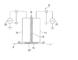
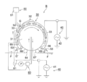
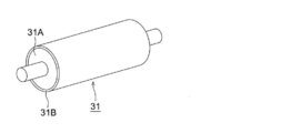
- FIG. 1 It is a schematic sectional drawing of a dielectric material film laminated body. It is the schematic which showed an example of the jet-type atmospheric pressure plasma discharge processing apparatus. It is the schematic which shows an example of the atmospheric pressure plasma discharge processing apparatus of the system which processes a base material between counter electrodes. It is a schematic perspective view which shows an example of the roll rotating electrode shown in FIG. It is a schematic perspective view which shows an example of the fixed electrode shown in FIG.
- FIG. 1 is a schematic sectional view of a dielectric film laminate.
- 1 indicates a dielectric film laminate.
- 101 shows a base material.
- Reference numeral 102 denotes a dielectric film laminated film.
- the dielectric film laminated film 102 has a configuration in which a high refractive index dielectric film 102a and a low refractive index dielectric film 102b are alternately laminated on at least one surface of a substrate 101.
- the order of lamination may be base material / high refractive index dielectric film 102a / low refractive index dielectric film 102b, or base material / low refractive index dielectric film 102b / high refractive index dielectric film 102a. Also good.
- This figure shows the case of base material / high refractive index dielectric film 102a / low refractive index dielectric film 102b.
- a lower layer containing an ultraviolet absorber may be provided between the base material and the dielectric film.
- binder Materials for forming the lower layer using the physical properties of the binder
- the binder used for the lower layer There are no particular restrictions on the binder used for the lower layer.
- vinyl chloride resins such as polyurethane, polyester, vinyl chloride copolymer, vinyl chloride resins such as vinyl chloride-vinyl acetate copolymer, polyolefin resins such as butadiene-acrylonitrile copolymer, polyvinyl butyral, etc.
- Polyvinyl acetal resin cellulose resin such as nitrocellulose, styrene resin such as styrene-butadiene copolymer, acrylic resin such as polymethyl methacrylate, polyamide, phenol resin, epoxy resin, phenoxy resin, polyvinyl butyral, polyvinyl aceto
- acetal resins such as acetal and polyvinyl formal
- water-soluble resins such as polyvinyl alcohol and gelatin.
- binder When the binder is cured to control the hardness and flexibility, there are no particular restrictions on the binder, but there are, for example, acrylate compounds.
- polyfunctional acrylates include pentaerythritol hexa (meth) acrylate and dipentaerythritol hexa.
- the curing method is not particularly limited and can be performed by a known method.
- a conventionally known photopolymerization initiator can be used, for example, 2,2-dimethoxy-2-phenylacetophenone, acetophenone, benzophenone, xanthone, 3-methylacetophenone, 4-chlorobenzophenone 4,4'-dimethoxybenzophenone, benzoin propyl ether, benzyldimethyl ketal, N, N, N ', N'-tetramethyl-4,4'-diaminobenzophenone, 1- (4-isopropylphenyl) -2-hydroxy Examples include -2-methylpropan-1-one and other thioxant compounds.
- the energy ray source used for the above curing for example, a high-pressure mercury lamp, a halogen lamp, a xenon lamp, a nitrogen laser, an electron beam accelerator, a radioactive element, or the like is used.
- inorganic fine particles may be added from the viewpoint of controlling the adhesion with the substrate.
- the inorganic fine particles include silicon oxide, titanium oxide, aluminum oxide, tin oxide, indium oxide, ITO, zinc oxide, zirconium oxide, magnesium oxide, calcium carbonate, calcium carbonate, talc, clay, and calcined kaolin.
- the thickness of the lower layer is preferably 1 ⁇ m to 15 ⁇ m, more preferably 2 ⁇ m to 8 ⁇ m. This is because if the film thickness is thinner than 1 ⁇ m, the hardness is lowered, and if it is thicker than 15 ⁇ m, cracks are generated in the lower layer itself and the adhesion is lowered.
- the dielectric film laminate of the present invention has a typical structure optically designed so that dielectric films having different refractive indexes are alternately laminated to reflect ultraviolet rays or infrared rays.
- the low refractive index is defined as a range in which the refractive index for light having a wavelength of 633 nm is 1.2 or more and less than 1.6.
- the refractive index is in the range of 1.5 or more and less than 1.45.
- High refractive index is defined as a range in which the refractive index for light having a wavelength of 633 nm is 1.6 or more and less than 2.9.
- the refractive index is preferably in the range of 1.70 or more and less than 2.7.
- a spectrophotometer 1U-4000 type (manufactured by Hitachi, Ltd.) is used to measure the reflectance under the condition of regular reflection at 5 degrees.
- the back surface on the observation side is roughened and then light absorption processing is performed using a black spray to prevent reflection of light on the back surface of the film and reflectivity (for wavelengths from 400 nm to 700 nm). Measurements were made.
- the optical film thickness is calculated from the ⁇ / 4 value of the spectrum, and based on this, the refractive index at 633 nm is calculated, or an automatic birefringence meter (manufactured by Oji Scientific Instruments, KOBRA-21ADH) is used.
- 10 points can be measured at a wavelength of 590 nm, a three-dimensional refractive index measurement can be performed, and the refractive index can be measured.
- the latter method is used. The refractive index values measured in the above were used.
- the dielectric film laminated film 102 is formed by forming one or more sets of units composed of a low refractive index dielectric film 102b and a high refractive index dielectric film 102a on the substrate 101.
- a unit or more units may be formed, and can be appropriately selected as necessary.
- V When the carbon concentration of the low refractive index dielectric film 102b is V, V is 6.5 ⁇ V ⁇ 40.0. A more preferable range is 10.0 ⁇ V ⁇ 35.0.
- the carbon concentration V of the dielectric film having a low refractive index is less than 6.5, the entire film itself is not soft enough and the cushioning property is insufficient, and the balance with the weight of the film laminated on the upper layer when laminated. This is not preferable because cracks occur in any of the entire laminated film. If the carbon concentration V of the low-refractive index dielectric film exceeds 40.0, the entire film itself becomes too soft, and when it is laminated, any of the entire laminated film cannot withstand the weight of the film laminated on the upper layer. This is not preferable because cracks occur. That is, it was found that cracks after lamination were not caused by setting the carbon concentration V of the low refractive index dielectric film to 6.5 ⁇ V ⁇ 40.0.
- Carbon concentration indicates the carbon content and is calculated by the following XPS method and is defined below.
- Carbon concentration (rate) number of carbon atoms / number of all atoms ⁇ 100
- ESCALAB-200R manufactured by VG Scientific, Inc. was used in the present invention. Specifically, Mg was used for the X-ray anode, and measurement was performed at an output of 600 W (acceleration voltage: 15 kV, emission current: 40 mA). The energy resolution was set to be 1.5 eV to 1.7 eV when defined by the half width of a clean Ag3d5 / 2 peak.
- the range of binding energy from 0 eV to 1100 eV was measured at a data acquisition interval of 1.0 eV to determine what elements were detected.
- the data acquisition interval was set to 0.2 eV, and the photoelectron peak giving the maximum intensity was subjected to narrow scan, and the spectrum of each element was measured.
- the obtained spectrum is COMMON DATA PROCESSING SYSTEM (Ver. 2.3 or later is preferable) manufactured by VAMAS-SCA-JAPAN in order not to cause a difference in content calculation results due to differences in measuring devices or computers.
- the processing was performed with the same software, and the content values of the elements (carbon, oxygen, silicon, titanium, etc.) of each analysis target were determined as atomic concentration (at%).
- the difference in hardness measured by the nanoindentation method between the low-refractive index dielectric film 102b and the high-refractive index dielectric film 102a is 1.4 GPa to 3.0 GPa in consideration of cracking prevention, haze stability, and the like. Is preferred.
- the difference in hardness between the low refractive index and the high refractive index dielectric is less than 1.4 GPa, the difference in hardness between the low refractive index and the high refractive index dielectric film is small. Stress is concentrated at the interface between the dielectric film and the dielectric film having a high refractive index, and as a result, cracks tend to occur. It has been found that cracks with various shapes are generated, and micro crack spaces are generated in the film, so that the heat shielding performance is deteriorated.
- the difference in hardness measured by the nanoindentation method is preferably 1.4 GPa to 3.0 GPa.
- the nano-indentation method is to continuously load and unload an indenter with a very small load on a sample, and measure the hardness (Hardness, hereinafter abbreviated as H) from the obtained load-displacement curve. Is the method.
- the hardness (H) of nanoindentation represents the value of the hardness of the direct surface of the sample. Therefore, the hardness (H) of nanoindentation is suitable as an index of surface hardness.
- the hardness (H) of the low-refractive index dielectric film 102b and the high-refractive index dielectric film 102a was measured by attaching a sample to a Nanoscope III manufactured by Digital Instruments, using a Triboscope manufactured by Hystron. For the measurement, a triangular pyramid diamond indenter called a Belkovic indenter (tip ridge angle 142.3 °) is used as an indenter.
- a triangular pyramid-shaped diamond indenter was applied to the sample surface at a right angle, a load was gradually applied, and the load was gradually returned to 0 after reaching the maximum load.
- the value P / A obtained by dividing the maximum load P at this time by the projected area A of the indenter contact portion was calculated as the hardness (H).
- the maximum load condition at this time is 100 ⁇ N. Details of the principle of surface hardness measurement by the nanoindentation method are described in, for example, Handbook of Micro / Nano Tribology (CRC edited by Bharat Bhushan).
- the hardness of the low refractive index dielectric film and the high refractive index dielectric film was measured as follows. A dielectric film was formed independently on the substrate used in the examples, and measured individually by the nanoindentation method.
- the dielectric film may be laminated on only one side or both sides of the substrate.
- stress may concentrate on only one side of the substrate, which may be disadvantageous in cracking and haze performance. In that case, you may laminate
- the thickness of one layer of the low refractive index dielectric film 102b is preferably 120 nm to 250 nm in consideration of heat shielding properties.
- the thickness of one layer of the high refractive index dielectric film 102a is preferably 50 nm to 200 nm in consideration of heat shielding properties.
- the total thickness of the dielectric film laminate 102 is preferably 500 nm or more, and more preferably 500 nm to 2000 nm. More preferably, it is 700 nm to 1500 nm. In addition, when the dielectric film laminated body is formed in both surfaces, let the total of both surfaces be a total thickness.
- the film thickness measurement of the low refractive index dielectric film 102b, the high refractive index dielectric film 102a, and the dielectric film stack 102 is, for example, a USB simple film thickness measurement device Solid Lambda Thickness ( Spectra Corp.).
- the cross-sectional portion of the formed dielectric film laminate can be cut out using a microtome or the like, and the cross-sectional portion can be observed using an electron microscope or the like to obtain the total film thickness of the dielectric film laminate. . In this invention, it measured using the latter method.
- the low-refractive index dielectric film 102b and the high-refractive index dielectric film 102a may be infrared and ultraviolet reflection films, but are preferably infrared reflection films.
- a vapor phase growth method is preferable, and further, a vacuum deposition method, a sputtering method, an ion plating method, a catalytic chemistry method.
- a vacuum deposition method a vapor deposition (Cat-CVD) method, a plasma CVD method, and an atmospheric pressure plasma method.
- a gas is introduced into the discharge space under atmospheric pressure or a pressure in the vicinity thereof, the gas is excited by forming a high-frequency electric field in the discharge space, and the substrate is exposed to the gas excited in the plasma state.
- the gas is preferably formed by an atmospheric pressure plasma method for forming a dielectric film on the substrate.
- thermoplastic resin film As the base material used in the present invention, a thermoplastic resin film is preferably used.
- the thermoplastic resin film can be used without any particular limitation. Examples thereof include polyethylene terephthalate, polyethylene naphthalate, polyimide, polyamide, polypropylene, polyethylene, polyvinyl chloride, acetate, nylon, polyetherimide, polycarbonate, polysulfone, polyphenylene oxide, polyphenylene sulfide, and cellulose esters.
- the dielectric film When the dielectric film is provided on the base material used in the present invention, it may be provided from a high refractive index dielectric film or a low refractive index dielectric film, and there is no particular limitation. There is no particular limitation whether the last laminated film is a high refractive index dielectric film or a low refractive index dielectric film. However, it is preferable that the low-refractive index dielectric film and the high-refractive index dielectric film have an alternating configuration as the infrared reflective film.
- thermoplastic resin films are provided with a dielectric film (low refractive index dielectric film or high refractive index dielectric film) in order to improve adhesion to the dielectric film (low refractive index dielectric film or high refractive index dielectric film). It is preferable to perform easy adhesion treatment or undercoat layer coating on the side on which the film is provided. Examples of the easy adhesion treatment include corona discharge treatment, flame treatment, and ultraviolet irradiation treatment. Examples of the undercoat layer include gelatin, latex, and a layer containing a polymer binder.
- a material for forming the low-refractive index dielectric film and the high-refractive index dielectric film related to the dielectric film laminate of the present invention a material mainly composed of metal oxide, nitride oxide, or nitride can be preferably used. .
- the low refractive index dielectric film having a low refractive index is preferably composed mainly of an oxide, nitride oxide, or nitride containing at least Si or Al, and particularly composed of silicon oxide. Furthermore, materials mainly composed of fluorides of calcium, barium, lithium and magnesium can be used.
- Examples of the main component for forming the low refractive index dielectric film related to the dielectric film laminate of the present invention include fluorine-containing (meth) acrylate, silicone resin, and silicon oxide such as SiO 2. I can do it. These may be contained alone or in combination of two or more.
- the main component is an oxide, nitride oxide, or nitride containing at least Zn, Ti, Sn, In, Nb, Si, Ta or Al. It is preferable to configure.
- Specific examples of the main component of the high refractive index dielectric film include titanium oxide, zinc oxide, indium oxide, tin oxide, indium and tin oxide, and magnesium oxide.
- metal oxides such as oxides, aluminum oxides, zirconium oxides, niobium oxides, and cerium oxides. These may be contained alone or in combination of two or more. These metal oxides may be a double oxide in which two or more metal oxides are combined.
- titanium oxide (IV) TiO 2
- titanate indium tin oxide
- ITO indium tin oxide
- ZnO zinc oxide
- oxidation etc.
- tin (SnO 2) it can be exemplified such as suitable. These may be contained alone or in combination of two or more.
- the raw material compound of the dielectric film used in the atmospheric pressure plasma method for forming the low refractive index dielectric film and the high refractive index dielectric film related to the dielectric film laminate of the present invention on the substrate will be further described.
- the low-refractive index dielectric film and the high-refractive index dielectric film can be obtained by selecting conditions such as an organic metal compound, a decomposition gas, a decomposition temperature, and an input power as raw materials (also referred to as raw materials) in the atmospheric pressure plasma method.
- a dielectric film having a refractive index different from that of a ceramic layer mainly composed of an oxide, nitride oxide, or nitride containing Al can be selected by selecting conditions such as an organic metal compound, a decomposition gas, a decomposition temperature, and an input power as raw materials (also referred to as raw materials) in the atmospheric pressure plasma method.
- silicon oxide is generated.
- silazane or the like is used as a raw material compound, silicon oxynitride is generated. This is because highly active charged particles and active radicals exist in the plasma space at a high density, so that multistage chemical reactions are accelerated at high speed in the plasma space, and the elements present in the plasma space are thermodynamic. This is because it is converted into an extremely stable compound in a very short time.
- a raw material for forming such a dielectric film as long as it is a silicon compound, it may be in a gas, liquid, or solid state at normal temperature and pressure.
- gas it can be introduced into the discharge space as it is, but in the case of liquid or solid, it is used after being vaporized by means such as heating, bubbling, decompression or ultrasonic irradiation.
- the solvent may be diluted with a solvent, and an organic solvent such as methanol, ethanol, n-hexane or a mixed solvent thereof can be used as the solvent. Since these diluted solvents are decomposed into molecular and atomic forms during the plasma discharge treatment, the influence can be almost ignored.
- silicon compounds examples include silane, tetramethoxysilane, tetraethoxysilane, tetra n-propoxysilane, tetraisopropoxysilane, tetra n-butoxysilane, tetra t-butoxysilane, dimethyldimethoxysilane, dimethyldiethoxysilane, Diethyldimethoxysilane, diphenyldimethoxysilane, methyltriethoxysilane, ethyltrimethoxysilane, phenyltriethoxysilane, (3,3,3-trifluoropropyl) trimethoxysilane, hexamethyldisiloxane, bis (dimethylamino) dimethylsilane Bis (dimethylamino) methylvinylsilane, bis (ethylamino) dimethylsilane, N, O-bis (trimethylsilyl) acet
- Examples of the aluminum compound include aluminum ethoxide, aluminum triisopropoxide, aluminum isopropoxide, aluminum n-butoxide, aluminum-butoxide, aluminum t-butoxide, aluminum acetylacetonate, triethyldialuminum tri-s-butoxide, and the like. It is done.
- a decomposition gas for decomposing the source gas containing silicon or aluminum to obtain a silicon oxide or aluminum oxide film hydrogen gas, methane gas, acetylene gas, carbon monoxide gas, carbon dioxide gas, nitrogen gas, Ammonia gas, nitrous oxide gas, nitrogen oxide gas, nitrogen dioxide gas, oxygen gas, water vapor, fluorine gas, hydrogen fluoride, trifluoroalcohol, trifluorotoluene, hydrogen sulfide, sulfur dioxide, carbon disulfide, chlorine gas, etc.
- hydrogen gas, methane gas, acetylene gas, carbon monoxide gas, carbon dioxide gas, nitrogen gas, Ammonia gas, nitrous oxide gas, nitrogen oxide gas, nitrogen dioxide gas, oxygen gas, water vapor, fluorine gas, hydrogen fluoride, trifluoroalcohol, trifluorotoluene hydrogen sulfide, sulfur dioxide, carbon disulfide, chlorine gas, etc.
- a dielectric film containing silicon oxide, nitride, carbide or the like can be obtained by appropriately selecting a source gas containing silicon and a decomposition gas.
- these reactive gases tend to be mainly in a plasma state.
- the discharge gas is mixed and the gas is sent to the plasma discharge generator.
- nitrogen gas or 18th group atom of the periodic table specifically, helium, neon, argon, krypton, xenon, radon, etc. are used. Among these, nitrogen, helium, and argon are preferably used.
- the above-described discharge gas and reactive gas are mixed and supplied to a plasma discharge generator (plasma generator) as a low-refractive-index dielectric film and a high-refractive-index dielectric film forming (mixed) gas, thereby providing a low-refractive-index dielectric film. Then, a high refractive index dielectric film is formed.
- a plasma discharge generator plasma generator
- the ratio of the discharge gas and the reactive gas varies depending on the properties of the film to be obtained, it is preferable to supply the reactive gas with the ratio of the discharge gas being 50% or more of the entire mixed gas.
- the above-mentioned organosilicon compound is further combined with oxygen gas or nitrogen gas at a predetermined ratio, and O atoms and A low refractive index dielectric film and a high refractive index dielectric film mainly composed of silicon oxide containing at least one of N atoms and Si atoms can be obtained.
- a dielectric film is formed by supplying a gas containing a body film forming gas and a discharge gas, exciting the gas by forming a high-frequency electric field in the discharge space, and exposing the gas to the excited gas.
- a dielectric film having a different refractive index can be continuously formed by feeding polyethylene naphthalate (PEN), which is a web-shaped resin support, from a roll-shaped original winding.
- PEN polyethylene naphthalate
- the high frequency referred to in the present invention means one having a frequency of at least 0.5 kHz.
- the atmospheric pressure plasma method used for forming the low refractive index dielectric film and the high refractive index dielectric film related to the dielectric film laminate of the present invention is a plasma CVD method performed under atmospheric pressure or a pressure in the vicinity thereof.
- the atmospheric pressure or the pressure in the vicinity thereof is about 20 kPa to 110 kPa, and 93 kPa to 104 kPa is preferable in order to obtain the good effects described in the present invention.
- the frequency of the high-frequency electric field is preferably 1 kHz to 2500 MHz
- the supplied power is preferably 1 W / cm 2 to 50 W / cm 2
- the frequency is 50 kHz or more
- the supplied power is 5 W / cm. More preferably, it is 2 or more.
- two or more electric fields having different frequencies are applied to the discharge space and superimposed.
- the present invention is not limited to this, and both pulse waves may be used, one may be continuous waves and the other may be pulse waves. Further, it may have a third electric field having a different frequency.
- a first power source that forms a high tatami-frequency electric field having a frequency ⁇ 1 is connected to the first electrode constituting the counter electrode, and the second An atmospheric pressure plasma discharge processing apparatus in which a second power source for forming a high-frequency electric field having a frequency ⁇ 2 is connected to the electrode is used.
- an electric field may be formed by connecting two power sources to the first power source.
- the frequency of the first power source is 1 kHz to 1 MHz, and 200 kHz or less can be preferably used.
- the electric field waveform may be a continuous wave or a pulse wave.
- the frequency of the second power source is preferably 1 MHz to 2500 MHz, and more preferably 800 kHz or more.
- the first electrode, the first power source, or any one of them is a first filter that makes it difficult to pass a high-frequency electric field current from the second power source, and the second electrode, the second power source, or any one between them. It is preferable to connect a second filter.
- the strength of the electric field at which discharge starts is the lowest electric field intensity that can cause discharge in the discharge space (electrode configuration, etc.) and reaction conditions (gas conditions, etc.) used in the actual thin film formation method.
- the discharge start electric field strength varies somewhat depending on the gas type supplied to the discharge space, the dielectric type of the electrode, the distance between the electrodes, and the like, but is controlled by the discharge start electric field strength of the discharge gas in the same discharge space.
- the applied electric field strength and the discharge start electric field strength are those measured by the following methods.
- V1 and V2 Measuring method of applied electric field strengths V1 and V2 (unit: kV / mm)
- a high frequency voltage probe (P6015A) is installed in each electrode part, and an output signal of the high frequency voltage probe is connected to an oscilloscope (Tektronix, TDS3012B), The electric field strength at a predetermined time is measured.
- Discharge gas is supplied between the electrodes, the electric field strength between the electrodes is increased, and the electric field strength at which discharge starts is defined as the discharge start electric field strength IV. .
- the measuring instrument is the same as the applied electric field strength measurement.
- the above atmospheric pressure plasma discharge treatment apparatus includes gas supply means for supplying a discharge gas and a dielectric film forming gas between the counter electrodes. Furthermore, it is preferable to have an electrode temperature control means for controlling the temperature of the electrode.
- the atmospheric pressure plasma discharge treatment apparatus used in the present invention discharges between the counter electrodes, puts the gas introduced between the counter electrodes into a plasma state, and places the gas between the counter electrodes or between the electrodes. By exposing the transferred resin support to the plasma state gas, a dielectric film is formed on the resin support.
- the atmospheric pressure plasma discharge treatment apparatus discharges between the counter electrodes similar to the above, excites the gas introduced between the counter electrodes or puts it into a plasma state, and excites or jets the gas outside the counter electrode.
- a jet system in which a dielectric film is formed on a resin support by blowing out gas in a plasma state and exposing a resin support (which may be stationary or transferred) in the vicinity of the counter electrode There is a device.
- FIG. 2 is a schematic view showing an example of a jet type atmospheric pressure plasma discharge treatment apparatus.
- the jet type atmospheric pressure plasma discharge processing apparatus has a gas supply means (see FIG. 2) and an electrode temperature adjusting means (see FIG. 2). It is a device.
- the atmospheric pressure plasma discharge processing apparatus A has a counter electrode composed of a first electrode 11 and a second electrode 12, and the frequency from the first power source 21 is from the first electrode 11 between the counter electrodes.
- a high frequency electric field of ⁇ 1 is applied, and a high frequency electric field of frequency ⁇ 2 from the second power source 22 is applied from the second electrode 12.
- the dielectric film forming gas G described above is introduced into the gap (discharge space) 13 between the first electrode 11 and the second electrode 12 from the gas supply means 50 as shown in FIG.
- the first power source 21 and the second power source 22 form the above-described high-frequency electric field between the first electrode 11 and the second electrode 12 to generate a discharge, and the dielectric film forming gas G is in a plasma state while the counter electrode is Blowing out in the form of a jet on the lower side (lower side of the paper), the processing space created by the lower surface of the counter electrode and the base material F is filled with gas G ° in the plasma state, and the base material is unwound (unwinding) (not shown)
- a dielectric film (a low-refractive index dielectric film or a high-refractive index dielectric film) is formed near the processing position 14 on the base material F that is unwound from the substrate and conveyed from the previous process.
- the medium heats or cools the electrode from the electrode temperature adjusting means 60 (see FIG. 3) through the pipe.
- the physical properties and composition of the obtained dielectric film may change. It is desirable to control.
- the temperature control medium an insulating material such as distilled water or oil is preferably used.
- G ′ represents the treated exhaust gas after the discharge treatment.
- a plurality of jet-type atmospheric pressure plasma discharge treatment apparatuses are arranged in parallel with the transport direction of the base material F, and simultaneously discharge a gas in the same plasma state, so that a plurality of dielectric films (low refractive index dielectrics) are formed at the same position.
- Body film or high refractive index dielectric film can be formed, and a desired film thickness can be formed in a short time.
- a plurality of units are arranged in parallel with the transport direction of the base material F, and different dielectric film (low refractive index dielectric film or high refractive index dielectric film) forming gas is supplied to each device so that gases in different plasma states are supplied. If jetting is performed, a laminated dielectric film of dielectric films having different refractive indices can be formed.
- FIG. 3 is a schematic view showing an example of an atmospheric pressure plasma discharge treatment apparatus of a type that treats a substrate between opposed electrodes.
- the atmospheric pressure plasma discharge treatment apparatus B is an apparatus having at least a plasma discharge treatment vessel 30, an electric field applying means 40 having two power sources, a gas supply means 50, and an electrode temperature adjusting means 60.
- the plasma discharge treatment vessel 30 is formed between a counter electrode 33 between a roll rotating electrode (first electrode) 31 and a fixed electrode group (second electrode) 32 (hereinafter, the counter electrode is also referred to as a discharge space 33).
- a dielectric film is formed by a discharge treatment (low refractive index dielectric film or high refractive index dielectric film).
- the roll rotating electrode (first electrode) 31 has a frequency ⁇ 1 from the first power source 41.
- a high-frequency electric field is applied, and a second high-frequency electric field having a frequency ⁇ 2 is applied to the fixed electrode group 32 from the second power source 42.
- the roll rotating electrode (first electrode) 31 may be the second electrode, and the fixed electrode group 32 may be the first electrode.
- the first power source is connected to the first electrode, and the second power source is connected to the second electrode.
- the dielectric film forming gas G generated by the gas generator 51 of the gas supply means 50 is introduced into the plasma discharge processing vessel 30 from the air supply port 52 while the flow rate is controlled by a gas flow rate adjusting means (not shown).
- the substrate F is unwound from the original winding (not shown) and conveyed, or is conveyed in the direction of the arrow from the previous process and is accompanied by the nip roll 65 through the guide roll 64 and the substrate. Etc., and is transferred to the fixed electrode group (second electrode) 32 while being wound while being in contact with the roll rotating electrode (first electrode) 31.
- the base material F forms a dielectric film with gas in a plasma state while being wound while being in contact with the roll rotating electrode (first electrode) 31.
- a plurality of fixed electrodes are provided along a circumference larger than the circumference of the roll electrode, and the discharge area of the fixed electrode is all opposed to the roll rotating electrode (first electrode) 31. It is represented by the sum of the areas of the surfaces of the fixed electrode facing the roll rotating electrode (first electrode) 31.
- the base material F passes through the nip roll 66 and the guide roll 67 and is wound up by a winder (not shown) or transferred to the next process. Discharged treated exhaust gas G ′ is discharged from the exhaust port 53.
- a medium whose temperature is adjusted by the electrode temperature adjusting means 60 is supplied to the liquid feed pump P. Then, the pipe 61 is sent to both electrodes, and the temperature is adjusted from the inside of the electrode.
- Reference numerals 68 and 69 denote partition plates for partitioning the plasma discharge processing vessel 30 from the outside world.
- FIG. 4 is a schematic perspective view showing an example of the roll rotating electrode shown in FIG.
- the roll electrode (first electrode) 31 has a conductive metallic base material 31A and a dielectric 31B coated thereon.
- the temperature adjusting medium water or silicon oil
- FIG. 5 is a schematic perspective view showing an example of the fixed electrode shown in FIG.
- the fixed electrode group (second electrode) 32 has a conductive metallic base material 32A and a dielectric 32B coated thereon.
- a temperature adjusting medium such as water or silicon oil
- the shape of the fixed electrode group (second electrode) 32 is not particularly limited, and may be a cylindrical electrode or a rectangular tube electrode.
- a roll electrode (first electrode) 31 and a fixed electrode group (second electrode) 32 are respectively provided with a dielectric 31B and a dielectric on a conductive metallic base material 31A and a metallic base material 32A.
- the ceramic body 32B is thermally sprayed and then sealed with an inorganic compound sealing material.
- the ceramic dielectric may be covered by about 1 mm with a single wall.
- As the ceramic material used for thermal spraying alumina, silicon nitride, or the like is preferably used. Among these, alumina is particularly preferable because it is easily processed.
- the dielectric layer may be a lining-processed dielectric provided with an inorganic material by lining.
- Examples of the conductive metallic base material 31A and the metallic base material 32A include titanium metal or titanium alloy, silver, platinum, stainless steel, aluminum, iron, and other metals, composite materials of iron and ceramics, or aluminum and ceramics. And composite materials.
- the distance between the opposing first electrode and second electrode is the shortest distance between the surface of the dielectric and the surface of the conductive metallic base material of the other electrode when a dielectric is provided on one of the electrodes.
- a dielectric is provided on both electrodes, it means the shortest distance between the dielectric surfaces.
- the distance between the electrodes is determined in consideration of the thickness of the dielectric provided on the conductive metal base material, the magnitude of the applied electric field strength, the purpose of using the plasma, etc. From the viewpoint of performing, it is preferably 0.1 mm to 20 mm, particularly preferably 0.5 mm to 5 mm.
- the plasma discharge treatment vessel 30 is preferably a treatment vessel made of Pyrex (registered trademark) glass or the like, but may be made of metal as long as it can be insulated from the electrodes.
- polyimide resin or the like may be attached to the inner surface of an aluminum or stainless steel frame, and ceramic spraying may be performed on the metal frame to achieve insulation.
- SPG5-4500 5 kHz
- Shinko Electric Co., Ltd. AGI-023 (15 kHz) manufactured by Kasuga Electric Co., Ltd.
- PHF-6k manufactured by HEIDEN Laboratory (100 kHz *)
- commercially available products such as CF-2000-200k (200 kHz) manufactured by Pearl Industry, and any of them can be used.
- the second power source (high frequency power source)
- commercially available products such as CF-2000-800k (800 kHz), CF-5000-13M (13.56 MHz), CF-2000-150M (150 MHz) manufactured by Pearl Industries, Ltd. Any of these can be preferably used.
- * indicates a HEIDEN Laboratory impulse high-frequency power supply (100 kHz in continuous mode). Other than that, it is a high-frequency power source that can apply only a continuous sine wave.
- an electrode capable of maintaining a uniform and stable discharge state by applying such an electric field to an atmospheric pressure plasma discharge treatment apparatus.
- the power applied between the electrodes facing each other is such that power (power density) of 1 W / cm 2 or more is supplied to the second electrode (second high-frequency electric field) to excite the discharge gas to generate plasma.
- the energy is applied to the dielectric film forming gas to form the dielectric film.
- the upper limit value of the power supplied to the second electrode is preferably 50 W / cm 2 , more preferably 20 W / cm 2 .
- the lower limit is preferably 1.0 W / cm 2 .
- the discharge area (cm 2 ) refers to an area in a range where discharge occurs between the electrodes.
- the film quality can be further improved.
- power density power density
- the film quality can be further improved.
- it is 5 W / cm 2 or more.
- the upper limit value of the power supplied to the first electrode is preferably 50 W / cm 2 .
- the waveform of the high-frequency electric field is not particularly limited.
- a continuous sine wave continuous oscillation mode called a continuous mode
- an intermittent oscillation mode called ON / OFF intermittently called a pulse mode
- the second electrode side second
- the high-frequency electric field is preferably a continuous sine wave because a denser and better quality film can be obtained.
- a low-refractive index dielectric film or a high-refractive index dielectric film having a different refractive index supplies a gas containing a dielectric film forming gas and a discharge gas to the discharge space under atmospheric pressure or a pressure in the vicinity thereof.
- the dielectric film is formed by a dielectric film forming method in which the gas is excited by forming a high-frequency electric field in the discharge space and exposed to the excited gas.
- the discharge gas is nitrogen gas
- the high-frequency electric field applied to the discharge space is a superposition of the first high-frequency electric field and the second high-frequency electric field
- the frequency ⁇ 1 of the first high-frequency electric field The frequency ⁇ 2 of the second high-frequency electric field is high, and the relationship among the first high-frequency electric field strength V1, the second high-frequency electric field strength V2, and the discharge start electric field strength IV is V1 ⁇ IV> V2.
- V1> IV ⁇ V2 it is preferable that the relationship of V1> IV ⁇ V2 is satisfied, and the output density of the second high-frequency electric field is 1 W / cm 2 or more.
- the low refractive index dielectric film and the high refractive index dielectric film have different hardness, and the carbon concentration V of the low refractive index dielectric film is 6.5 ⁇ V ⁇ 40.
- the following effects were obtained by a dielectric film laminate in which low refractive index dielectric films having a relationship of 0.0 and high refractive index dielectric films were alternately laminated.
- Example 1 (Preparation of base material) A polyethylene terephthalate (PET) film having a thickness of 125 ⁇ m was prepared as a substrate.
- PET polyethylene terephthalate
- a coating solution for forming a lower layer containing an ultraviolet absorber as a light stabilizer having the following composition is prepared and applied using a micro gravure coater so that the film thickness after curing is 5 ⁇ m.
- hot air drying was performed stepwise at 80 ° C./110° C./125° C. (each zone was 30 sec) to provide a lower layer.
- 2- (2H-benzotriazol-2-yl) -4,6-di-t-pentylphenol (TINUVIN328; Ciba Japan Co., Ltd.), which is a benzotriazole-based ultraviolet absorber as an ultraviolet absorber.
- 5% by weight of decanedioic acid bis [2,2,6,6-tetramethyl-1 (octyloxy) -4-piperidinyl] ester (TINUVIN123; Ciba (Made by Japan Co., Ltd.) was blended in an amount of 5% by mass, diluted with methyl ethyl ketone to adjust the viscosity, and the main component (a) adjusted to a solid content of 20% by mass was obtained.
- a curing agent (b) obtained by adjusting adduct-type hexamethylene diisocyanate with methyl ethyl ketone so that the solid content was 75% by mass was obtained. 15 mass% of the said hardening
- curing agent (b) was added with respect to the said main ingredient (a), and the coating liquid for lower layer formation was prepared.
- a dielectric film laminate having the structure shown in Tables 1 and 2 was produced on the base material on which the prepared lower layer was formed by the atmospheric pressure plasma CVD method. 101 to 129.
- the thickness of the high-refractive index dielectric film and the low-refractive index dielectric film is determined by cutting the cross section of the formed dielectric film laminate with a microtome and observing the cross section with an electron microscope or the like. Indicates the value obtained.
- the refractive index of the low refractive index dielectric film and the high refractive index dielectric film was measured using an automatic birefringence meter (manufactured by Oji Scientific Instruments, KOBRA-21ADH) in an environment of 23 ° C. and 55% RH. The values obtained by measuring 10 locations at a wavelength of 590 nm and performing three-dimensional refractive index measurement are shown.
- the hardness of the low-refractive index dielectric film and the high-refractive index dielectric film is a value obtained by measuring the hardness when measured with a weight of 20 ⁇ N using ENT1100a manufactured by Elionix.
- the nanoindentation probe is a Berkovich indenter in which a diamond triangular pyramid with a tip radius of curvature of 25 nm or less, a ridge angle of 60 degrees, and a height of 100 ⁇ m is fixed to a base having a length of 350 ⁇ m, a width of 100 ⁇ m, a thickness of 13 ⁇ m, and a spring constant of 263 N / m. Was used.
- the carbon concentration of the low-refractive index dielectric film is measured using an XPS surface analyzer (ESCALAB-200R manufactured by VG Scientific), and the spectrum of each element obtained is a COMMON DATA PROCESSING SYSTEM (manufactured by VAMAS-SCA-JAPAN) ( Ver. 2.3 or later is preferable), and the processing is performed with the same software, and the content value of each analysis target element (carbon, oxygen, silicon, titanium, etc.) is changed to the atomic concentration: at%).
- a high refractive index dielectric film was formed under the following conditions using the atmospheric pressure plasma discharge treatment apparatus shown in FIG.
- ⁇ Low refractive index layer mixed gas composition > Discharge gas: Nitrogen 96.33% by volume Thin film forming gas: hexamethyldisiloxane 2.76% by volume Addition gas: Oxygen 0.91 vol% ⁇ Low refractive index layer deposition conditions> 1st electrode side Power supply type HEIDEN Laboratory 100kHz (continuous mode) PHF-6k Frequency 100kHz Output density 10 W / cm 2 (the voltage Vp at this time was 7 kV) Electrode temperature 120 ° C Second electrode side Power supply type Pearl Industry 13.56MHz CF-5000-13M Frequency 13.56MHz Output density 10 W / cm 2 (the voltage Vp at this time was 2 kV) Electrode temperature 90 ° C (Preparation of dielectric film laminate No.
- Dielectric film laminate No. 102 Dielectric film laminate No.
- the dielectric film laminate No. 1 was changed except that the low refractive index layer mixed gas composition for producing the low refractive index layer of 101 was changed as shown below. No. 101 was used to produce a dielectric film laminate. 102.
- ⁇ Low refractive index layer mixed gas composition > Discharge gas: Nitrogen 90.51% by volume Thin film forming gas: hexamethyldisiloxane 2.60% by volume Additive gas: oxygen 6.89 vol% (Preparation of dielectric film laminate No. 103) Dielectric film laminate No.
- the dielectric film laminate No. 1 was prepared except that the low refractive index layer mixed gas composition for producing the low refractive index layer of 101 was changed to the following. No. 101 was used to produce a dielectric film laminate. 103.
- dielectric film laminate No. 10 Dielectric film laminate No. 10 was prepared except that the thickness of the high refractive index dielectric film No. 101 was 80 nm and the thickness of the low refractive index dielectric film was 150 nm. A dielectric film laminate was prepared in the same manner as in 101, and dielectric film laminate No. 108.
- dielectric film laminate No. 10 Dielectric film lamination No. No. 102 dielectric film laminate No. 10 except that nine layers of high refractive index dielectric films and low refractive index dielectric films were alternately laminated.
- a dielectric film laminate was produced by the same method as that of the dielectric film laminate No. 102. 109.
- dielectric film laminate No. 110 Dielectric film laminate No. On one side of the same PET film as 101, dielectric film laminate No. The same lower layer as that in FIG. After providing the same high-refractive-index dielectric film as in 101, the dielectric film stack No. The same low-refractive-index dielectric film as 101 was provided, and the same high-refractive-index dielectric film was further provided. Furthermore, on the other side of the PET film, the dielectric film laminate No. The same lower layer as that in FIG. After providing the same high-refractive-index dielectric film as in 101, the dielectric film stack No. The same low refractive index dielectric film as that of No. 101 is provided, and the same high refractive index dielectric film is further provided. 110.
- dielectric film laminate No. 111 Dielectric film laminate No.
- dielectric film laminate No. 103 is provided with the same lower layer as that of the dielectric film laminate no. After providing the same high-refractive-index dielectric film as in FIG. The same low refractive index dielectric film as that of No. 103 is provided. The same high refractive index dielectric film as 103 was provided. Further, on the other side of the PET film, the dielectric film laminate No. 103 is provided with the same lower layer as that of the dielectric film laminate no. After providing the same high-refractive-index dielectric film as in FIG. The same low refractive index dielectric film as that of No. 103 is provided. The same high refractive index dielectric film as that of No. 103 is provided, and a dielectric film laminate having a total of six layers is manufactured. 111.
- Dielectric film laminate No. 112 Dielectric film laminate No. 110, except that no lower layer on both sides on the PET film is provided. A dielectric film laminate having the same configuration as that of No. 110 was prepared. 112.
- Dielectric film laminate No. 113 Dielectric film laminate No. Dielectric film laminate No. 1 except that no lower layer on both sides on the PET film of 111 is provided. A dielectric film laminate having the same structure as that of No. 111 was prepared. 113.
- Dielectric film laminate No. 114 (Preparation of dielectric film laminate No. 114 (comparative)) Dielectric film laminate No.
- the low refractive index dielectric film condition of 110 is the dielectric film laminate No. Dielectric film laminate No. 10 except that the low refractive index dielectric film condition of 105 was used.
- a dielectric film laminate having the same structure as that of No. 110 was prepared. 114.
- Dielectric film laminate No. 115 (Production of dielectric film laminate No. 115 (comparative)) Dielectric film laminate No.
- the low refractive index dielectric film condition of 110 is the dielectric film laminate No. Dielectric film laminate No. 10 except that the low refractive index dielectric film condition of 106 was used.
- a dielectric film laminate having the same structure as that of No. 110 was prepared. 115.
- dielectric film laminate No. 116 Dielectric film laminate No. On one side of PET film 110 and the lower layer, dielectric film laminate No. Dielectric film laminate No. 10 under the same low refractive index dielectric film conditions as in No. 110. Dielectric film stack No. 10 except that the same low refractive index dielectric film as that of No. 110 was provided. The same high-refractive-index dielectric film and low-refractive-index dielectric film as those of 110 are used. No. 101 was prepared to produce a dielectric film laminate. 116.
- Dielectric film laminate No. 110 on both sides of the PET film and the lower layer.
- Dielectric film laminate No. 10 under the same low refractive index dielectric film conditions as in No. 110.
- Dielectric film stack No. 10 except that the same low refractive index dielectric film as that of No. 110 was provided.
- the same high-refractive-index dielectric film and low-refractive-index dielectric film as those of 110 are used.
- No. 101 was prepared to produce a dielectric film laminate. 117.
- Dielectric film laminate No. 116 except that the lower layer of 116 is removed.
- a dielectric film laminate having the same structure as that of No. 116 was prepared. 118.
- Dielectric film laminate No. 119 Dielectric film laminate No. Dielectric film laminated body No. 1 except that the lower layer of 117 was removed. A dielectric film laminate having the same structure as that of No. 117 was prepared. 119.
- Dielectric film laminate No. 120 (Production of dielectric film laminate No. 120 (comparative)) Dielectric film laminate No.
- the low refractive index dielectric film condition of No. Dielectric film laminate No. 10 except that the low refractive index dielectric film condition of 105 was used.
- a dielectric film laminate having the same structure as that of No. 116 was prepared. 120.
- Dielectric film laminate No. 121 (comparative) Dielectric film laminate No.
- Dielectric film laminate No. 122 (Preparation of dielectric film laminate No. 122 (comparative)) Dielectric film laminate No.
- the low refractive index dielectric film condition of 117 is the dielectric film stack No. Dielectric film laminate No. 10 except that the low refractive index dielectric film condition of 105 was used.
- a dielectric film laminate having the same structure as that of No. 117 was prepared. 122.
- Dielectric film laminate No. 123 (Preparation of dielectric film laminate No. 123 (comparative)) Dielectric film laminate No.
- the low refractive index dielectric film condition of 117 is the dielectric film stack No. Dielectric film laminate No. 10 except that the low refractive index dielectric film condition of 106 was used.
- a dielectric film laminate having the same structure as that of No. 117 was prepared. 123.
- Dielectric film laminate No. 124 Dielectric film laminate No. 110 on the uppermost high-refractive-index dielectric material on one side of the dielectric film laminate No. 110.
- Dielectric film stack No. 101 under the low refractive index dielectric film condition of 101.
- Dielectric film stack No. 10 except that the same low refractive index dielectric film as that of No. 110 was provided.
- a dielectric film laminate having the same configuration as that of No. 110 was prepared. 124.
- Dielectric film laminate No. 110 on the uppermost high-refractive-index dielectrics on both surfaces of the dielectric film laminate No. 110.
- Dielectric film stack No. 101 under the low refractive index dielectric film condition of 101.
- Dielectric film stack No. 10 except that the same low refractive index dielectric film as that of No. 110 was provided.
- a dielectric film laminate having the same configuration as that of No. 110 was prepared. 125.
- Dielectric film laminate No. 126 (Preparation of dielectric film laminate No. 126 (comparative)) Dielectric film laminate No.
- the low-refractive-index dielectric film condition of 124 is the dielectric film stack No. Dielectric film laminate No. 10 except that the low refractive index dielectric film condition of 105 was used.
- a dielectric film laminate having the same structure as that of No. 124 was produced. 126.
- Dielectric film laminate No. 127 (Production of dielectric film laminate No. 127 (comparative)) Dielectric film laminate No.
- the low-refractive-index dielectric film condition of 124 is the dielectric film stack No. Dielectric film laminate No. 10 except that the low refractive index dielectric film condition of 106 was used.
- a dielectric film laminate having the same structure as that of No. 124 was produced. 127.
- Dielectric film laminate No. 128 (Production of dielectric film laminate No. 128 (comparative)) Dielectric film laminate No.
- the low refractive index dielectric film condition of 125 is designated as dielectric film stack No. Dielectric film laminate No. 10 except that the low refractive index dielectric film condition of 105 was used.
- a dielectric film laminate having the same structure as that of No. 125 was produced. 128.
- Dielectric film laminate No. 129 (Production of dielectric film laminate No. 129 (comparative)) Dielectric film laminate No.
- the low refractive index dielectric film condition of 125 is designated as dielectric film stack No. Dielectric film laminate No. 10 except that the low refractive index dielectric film condition of 106 was used.
- a dielectric film laminate having the same structure as that of No. 125 was produced. 129.
- Evaluation rank of crack resistance 5 No crack generation 4: Some cracks are generated, but there are no problems in use 3: Cracks are generated, but there are concerns in use 2: Cracks are generated, there are problems in use 1: Cracks are generated, usable No Haze Test Method The prepared sample was measured based on the light source D65 JIS 7361-1 using Nippon Denshoku Industries Co., Ltd. NDH 2000. The larger the value, the higher the haze value and the lower the visibility, and the lower the value, the better the visibility.
- the dielectric film laminate of the present invention in which the low refractive index dielectric film and the high refractive index dielectric film are alternately laminated on the substrate of the present invention has excellent performance in terms of crack resistance, haze, and heat shielding properties. It was confirmed that The effectiveness of the present invention was confirmed.
- dielectric film laminate No. 202 The dielectric film laminate No. 1 prepared in Example 1 except that the carbon concentration V40.0 of the low refractive index dielectric film was prepared by changing the volume% of the discharge gas nitrogen, the thin film forming gas, and the additive gas. A dielectric film laminate similar to that of No. 105 was prepared. 202.
- dielectric film laminated body No. No. 201 and 202 the results of testing the crack resistance, haze, and heat shielding performance by the same method as in Example 1 showed that the dielectric film laminate No. 201 was crack resistance 4, haze 2.1, and heat-shielding property 10.
- Dielectric film laminate No. 202 had a crack resistance of 3, a haze of 2.7, and a heat shielding property of 11.
- Example 3 The dielectric film laminate No. 1 produced in Example 1 was composed of 7 layers on one side, and the thickness of each layer was as follows, and the total thickness was 545 nm. A dielectric film laminate was prepared in the same manner as in 101.
Landscapes
- Chemical & Material Sciences (AREA)
- Inorganic Chemistry (AREA)
- General Chemical & Material Sciences (AREA)
- Chemical Kinetics & Catalysis (AREA)
- Engineering & Computer Science (AREA)
- Materials Engineering (AREA)
- Mechanical Engineering (AREA)
- Metallurgy (AREA)
- Organic Chemistry (AREA)
- Laminated Bodies (AREA)
Abstract
低屈折率誘電体膜と高屈折率誘電体膜とを交互に積層させて形成した、クラックの発生がなく、ヘーズの良好な誘電体膜積層体の提供するために、基材の上に、低屈折率誘電体膜と、高屈折率誘電体膜とが交互に積層された誘電体膜積層体において、前記低屈折率誘電体膜と、前記高屈折率誘電体膜との硬さが異なり、前記低屈折率誘電体膜の炭素濃度量をVとすると、6.5≦V≦40.0であることを特徴とする誘電体膜積層体。
Description
本発明は、樹脂支持体上に低屈折率誘電体膜と高屈折率誘電体膜とを交互に積層させて形成した誘電体膜積層体及び誘電体膜積層体の製造方法に関する。
従来より、高屈折率誘電体膜と低屈折率誘電体膜とを交互に積層して、多層膜構造による光学干渉効果を利用することにより、紫外線又は近赤外線領域等の遮断性能を発揮するものは公知である。例えば、特開2001-194526号公報には、高屈折率誘電体膜と低屈折率誘電体膜とを交互に積層した多層膜を基板上に形成した反射ミラーが知られている。
特開2002-110105号公報には、高屈折率誘電体膜と低屈折率誘電体膜とを交互に積層した多層膜フィルタを有する赤外発光ランプが知られている。特開2002-220262号公報においては、高屈折率誘電体膜と低屈折率誘電体膜とが交互に積層された赤外線反射フィルムをガラスとガラスとの間に挟時させた構造の熱線遮蔽ガラスが知られている。
高屈折率誘電体膜と低屈折率誘電体膜とを交互に積層した積層体膜は高屈折率誘電体膜と低屈折率誘電体膜の材料が異なるため、形成された膜の硬さが異なり、そのため積層させると、最終的に目視で観察出来るレベルのクラックが入ったり、クラックが入ることでのヘーズが劣化したり、反射特性が劣化したりすると言う問題があった。これらの問題に対してこれまでに検討がなされてきた。例えば、基板側から高屈折率誘電体膜、低屈折率誘電体膜の順に順次形成された下層の積層膜の内部応力を打ち消すべく、高屈折率誘電体膜の次ぎに緩衝膜を形成する方法が知られている(特許文献1参照。)。
しかしながら、特許文献1に記載の方法は、基材の種類と厚みが変化することと、緩衝膜自身の緩衝能力も変動することが判り、十分な改善には至っておらず、改善が望まれていた。
中屈折率誘電体膜、高屈折率誘電体膜、低屈折率誘電体膜の構成を有する赤外反射防止膜のクラックを防止するために低屈折率膜の厚さを変える方法が知られている(特許文献2参照。)。
しかしながら、特許文献2に記載の方法は、厚みの均一性を得ることが難しく、膜厚変動することで安定にクラックを防止することは出来ず、単に厚さを変えるだけでは不十分であることが判り十分な改善には至っておらず、改善が望まれていた。
この様な状況から、基材上に低屈折率誘電体膜と高屈折率誘電体膜とを交互に積層させて形成した、クラックの発生がなく、ヘーズの良好な誘電体膜積層体の開発が望まれている。
本発明は、上記状況に鑑みなされたものであって、その目的とするところは、低屈折率誘電体膜と高屈折率誘電体膜とを交互に積層させて形成した、クラックの発生がなく、ヘーズの良好な誘電体膜積層体及び誘電体膜積層体の製造方法を提供することである。
本発明の上記目的は、下記の構成により達成された。
1.基材の上に、低屈折率誘電体膜と、高屈折率誘電体膜とが交互に積層された誘電体膜積層膜を有する誘電体膜積層体において、前記低屈折率誘電体膜と、前記高屈折率誘電体膜との硬さが異なり、前記低屈折率誘電体膜の炭素濃度量をVとすると、6.5≦V≦40.0であることを特徴とする誘電体膜積層体。
2.前記低屈折率誘電体膜と高屈折率誘電体膜とのナノインデンテーション法で測定した硬さの差が、1.4GPaから3.0GPaであることを特徴とする前記1に記載の誘電体膜積層体。
3.前記誘電体膜積層膜が基材の片面、又は両面に設けられていることを特徴とする前記1又は2に記載の誘電体膜積層体。
4.前記誘電体膜積層膜の総厚が、500nm以上であることを特徴とする前記1から3の何れか1項に記載の誘電体膜積層体。
5.前記低屈折率誘電体膜と高屈折率誘電体膜とが赤外線反射膜であることを特徴とする前記1から4の何れか1項に記載の誘電体膜積層体。
6.基材上に、硬さの異なる低屈折率誘電体膜と高屈折率誘電体膜が交互に積層された誘電体膜積層膜を有する誘電体膜積層体の製造方法において、前記低屈折率誘電体膜及び前記高屈折率誘電体膜は、大気圧又は大気近傍の圧力下で、ガスを放電空間に導入し、前記放電空間に高周波電界を形成することによりガスをプラズマ状態とし、前記基材を前記プラズマ状態のガスに晒すことによって形成されたことを特徴とする誘電体膜積層体の製造方法。
7.前記低屈折率誘電体膜と前記高屈折率誘電体膜とのナノインデンテーション法で測定した硬さの差が、1.4GPaから3.0GPaであることを特徴とする前記6に記載の誘電体膜積層体の製造方法。
8.前記誘電体膜積層膜の総厚が、500nm以上であることを特徴とする前記6又は7に記載の誘電体膜積層体の製造方法。
低屈折率誘電体膜と高屈折率誘電体膜とを交互に積層させて形成した、クラックの発生がなく、ヘーズの良好な誘電体膜積層体及び誘電体膜積層体の製造方法を提供することが出来た。
以下、本発明を実施するための形態を図1から図5を参照しながら説明するが、本発明はこれらに限定されるものではない。
図1は誘電体膜積層体の概略断面図である。
図中、1は誘電体膜積層体を示す。101は基材を示す。102は誘電体膜積層膜を示す。誘電体膜積層膜102は、基材101の少なくとも片面に、高屈折率誘電体膜102aと低屈折率誘電体膜102bとを交互に積層させた構成を有している。積層する順番は基材/高屈折率誘電体膜102a/低屈折率誘電体膜102bであってもよいし、基材/低屈折率誘電体膜102b/高屈折率誘電体膜102aであってもよい。本図は基材/高屈折率誘電体膜102a/低屈折率誘電体膜102bの場合を示している。尚、基材と誘電体膜との間に紫外線吸収剤を含有した下層を設けてもよい。
下層はバインダーの物性を利用して形成する方法と、バインダーを硬化させて硬さと柔軟性をコントロールして形成する方法とが挙げられる。以下にこれらに使用する材料に付き説明する。
下層をバインダーの物性を利用して形成する場合の材料
下層に用いられるバインダーとしては特に制限はない。例えば、ポリウレタン、ポリエステル、塩化ビニル系共重合体等の塩化ビニル系樹脂、塩化ビニル-酢酸ビニル共重合体等の塩化ビニル系樹脂、ブタジエン-アクリロニトリル共重合体等のポリオレフィン系樹脂、ポリビニルブチラール等のポリビニルアセタール系樹脂、ニトロセルロース等のセルロース系樹脂、スチレン-ブタジエン共重合体等のスチレン系樹脂、ポリメチルメタクリレート等のアクリル系樹脂、ポリアミド、フェノール樹脂、エポキシ樹脂、フェノキシ樹脂、ポリビニルブチラール、ポリビニルアセトアセタール、ポリビニルホルマール等のアセタール系樹脂、及びポリビニルアルコール、ゼラチン等の水溶性樹脂等がある。
下層に用いられるバインダーとしては特に制限はない。例えば、ポリウレタン、ポリエステル、塩化ビニル系共重合体等の塩化ビニル系樹脂、塩化ビニル-酢酸ビニル共重合体等の塩化ビニル系樹脂、ブタジエン-アクリロニトリル共重合体等のポリオレフィン系樹脂、ポリビニルブチラール等のポリビニルアセタール系樹脂、ニトロセルロース等のセルロース系樹脂、スチレン-ブタジエン共重合体等のスチレン系樹脂、ポリメチルメタクリレート等のアクリル系樹脂、ポリアミド、フェノール樹脂、エポキシ樹脂、フェノキシ樹脂、ポリビニルブチラール、ポリビニルアセトアセタール、ポリビニルホルマール等のアセタール系樹脂、及びポリビニルアルコール、ゼラチン等の水溶性樹脂等がある。
バインダーを硬化させて硬さと柔軟性をコントロールして形成する場合
バインダーとして特に制限はないが、例えばアクリレート化合物があり、多官能アクリレートとしては、例えば、ペンタエリスリトールヘキサ(メタ)アクリレート、ジペンタエリスリトールヘキサ(メタ)アクリレート、ペンタエリスリトールペンタ(メタ)アクリレート、ジペンタエリスリトールペンタ(メタ)アクリレート、ペンタエリスリトール(メタ)テトラアクリレート、ジペンタエリスリトール(メタ)テトラアクリレート、ペンタエリスリトールトリ(メタ)アクリレート、ジペンタエリスリトールトリ(メタ)アクリレート、ペンタエリスリトールグリシジル(メタ)アクリレート、トリメチロールプロパントリ(メタ)アクリレート、及びこれらの誘導体、変性品等が挙げられる。これらは、単独で使用されてもよいし、2種類以上併用されても良い。
バインダーとして特に制限はないが、例えばアクリレート化合物があり、多官能アクリレートとしては、例えば、ペンタエリスリトールヘキサ(メタ)アクリレート、ジペンタエリスリトールヘキサ(メタ)アクリレート、ペンタエリスリトールペンタ(メタ)アクリレート、ジペンタエリスリトールペンタ(メタ)アクリレート、ペンタエリスリトール(メタ)テトラアクリレート、ジペンタエリスリトール(メタ)テトラアクリレート、ペンタエリスリトールトリ(メタ)アクリレート、ジペンタエリスリトールトリ(メタ)アクリレート、ペンタエリスリトールグリシジル(メタ)アクリレート、トリメチロールプロパントリ(メタ)アクリレート、及びこれらの誘導体、変性品等が挙げられる。これらは、単独で使用されてもよいし、2種類以上併用されても良い。
硬化する方法としては特に限定されず、公知の方法で行うことが出来る。例えば、紫外線照射により硬化させる場合は、従来公知の光重合開始剤を用いることが出来、例えば2,2-ジメトキシ-2-フェニルアセトフェノン、アセトフェノン、ベンゾフェノン、キサントン、3-メチルアセトフェノン、4-クロロベンゾフェノン、4,4′-ジメトキシベンゾフェノン、ベンゾインプロピルエーテル、ベンジルジメチルケタール、N,N,N′,N′-テトラメチル-4,4′-ジアミノベンゾフェノン、1-(4-イソプロピルフェニル)-2-ヒドロキシ-2-メチルプロパン-1-オン、その他チオキサント系化合物等が挙げられる。
上記の硬化に用いられるエネルギー線源としては、例えば、高圧水銀ランプ、ハロゲンランプ、キセノンランプ、窒素レーザー、電子線加速装置、放射性元素などの線源が使用される。
下層には基材との密着性をコントロールする観点として、無機微粒子を添加してもよい。無機微粒子としては、酸化珪素、酸化チタン、酸化アルミニウム、酸化スズ、酸化インジウム、ITO、酸化亜鉛、酸化ジルコニウム、酸化マグネシウム、炭酸カルシウム、炭酸カルシウム、タルク、クレイ、焼成カオリン等が挙げられる。
上記下層の厚みは、1μmから15μmが好ましく、より好ましくは2μmから8μmである。膜厚が、1μmより薄すぎると硬度が下がり、15μmより厚すぎると下層自体にクラックが発生し、密着性が低下するためである。
本発明の誘電体膜積層体は、屈折率の異なる誘電体膜を交互に積層して、紫外線又は赤外線を反射出来るように光学設計された代表的な構成である。
低屈折率とは、波長が633nmの光に対する屈折率が、1.2以上、1.6未満の範囲と定義する。好ましくは、屈折率が1.5以上、1.45未満の範囲である。
高屈折率とは、波長が633nmの光に対する屈折率が、1.6以上、2.9未満の範囲と定義する。好ましくは屈折率が1.70以上、2.7未満の範囲である。
屈折率は、例えば、分光光度計1U-4000型(日立製作所製)を用いて、5度正反射の条件にて反射率の測定を行う。測定は、観察側の裏面を粗面化処理した後、黒色のスプレーを用いて光吸収処理を行い、フィルム裏面での光の反射を防止して、反射率(400nmから700nmの波長について)の測定を行った。スペクトルのλ/4値より光学膜厚を算出し、それを基に、633nmにおける屈折率を算出する方法、或いは自動複屈折率計(王子計測機器(株)製、KOBRA-21ADH)を用いて、23℃、55%RHの環境下で、590nmの波長において10カ所測定し3次元屈折率測定を行い、屈折率を測定する方法を用いることが出来、本発明においては、後者の方法を用いて測定した屈折率値を用いた。
誘電体膜積層膜102は、低屈折率誘電体膜102bと高屈折率誘電体膜102aとからなる一組のユニットを、一組以上、基材101の上に形成したものであるが、二ユニット、或いはそれ以上のユニットが形成されていてもよく、必要に応じて適宜選択することが可能である。
低屈折率誘電体膜102bの炭素濃度量をVとすると、Vは6.5≦V≦40.0である。より好ましい範囲は10.0≦V≦35.0である。
低屈折率の誘電体膜の炭素濃度量Vが6.5未満の場合、膜自身全体の柔らかさが足らず、クッション性が不足し、積層した際に上層に積層された膜の重さとのバランスが悪くなることで積層膜全体の何れかでクラックが生じるため好ましくない。低屈折率誘電体膜の炭素濃度量Vが40.0を超えると、膜自身全体が柔らかくなりすぎ積層した際に上層に積層された膜の重さに耐えられずに積層膜全体の何れかでクラックが生じるため好ましくない。即ち、低屈折率誘電体膜の炭素濃度量Vを6.5≦V≦40.0にすることで積層後のクラックが生じないことが判った。
炭素濃度量とは炭素含有率を示し、下記のXPS法によって算出されるもので、以下に定義される。
炭素濃度量(率)(atomic concentration)=炭素原子の個数/全原子の個数×100
XPS表面分析装置は、本発明では、VGサイエンティフィックス社製ESCALAB-200Rを用いた。具体的には、X線アノードにはMgを用い、出力600W(加速電圧15kV、エミッション電流40mA)で測定した。エネルギー分解能は、清浄なAg3d5/2ピークの半値幅で規定した時、1.5eVから1.7eVとなるように設定した。
XPS表面分析装置は、本発明では、VGサイエンティフィックス社製ESCALAB-200Rを用いた。具体的には、X線アノードにはMgを用い、出力600W(加速電圧15kV、エミッション電流40mA)で測定した。エネルギー分解能は、清浄なAg3d5/2ピークの半値幅で規定した時、1.5eVから1.7eVとなるように設定した。
測定としては、先ず、結合エネルギー0eVから1100eVの範囲を、データ取り込み間隔1.0eVで測定し、いかなる元素が検出されるかを求めた。
次に、検出された、エッチングイオン種を除く全ての元素について、データの取り込み間隔を0.2eVとして、その最大強度を与える光電子ピークについてナロースキャンを行い、各元素のスペクトルを測定した。
得られたスペクトルは、測定装置、或いは、コンピュータの違いによる含有率算出結果の違いを生じせしめなくするために、VAMAS-SCA-JAPAN製のCOMMON DATA PROCESSING SYSTEM (Ver.2.3以降が好ましい)上に転送した後、同ソフトで処理を行い、各分析ターゲットの元素(炭素、酸素、珪素、チタン等)の含有率の値を原子数濃度(atomic concentration:at%)として求めた。
定量処理を行う前に、各元素についてCount Scaleのキャリブレーションを行い、5ポイントのスムージング処理を行った。定量処理では、バックグラウンドを除去したピークエリア強度(cps*eV)を用いた。バックグラウンド処理には、Shirleyによる方法を用いた。このShirley法については、D.A.Shirley,Phys.Rev.,B5,4709(1972)を参考にすることが出来る。
低屈折率誘電体膜102bと高屈折率誘電体膜102aとのナノインデンテーション法で測定した硬さの差は、クラックの発生防止、ヘーズ安定性等を考慮し、1.4GPaから3.0GPaが好ましい。
低屈折率と高屈折率の誘電体の硬さの差が1.4GPa未満の場合は、低屈折率と高屈折率の誘電体膜同士の硬さの差が少ないために、低屈折率の誘電体膜と高屈折率の誘電体膜の界面に応力が多大に集中発生し、その結果クラックが発生する傾向になる。様々な形状のクラックが発生する方向になり、膜内にミクロなクラック空間が生じることで、遮熱性能が劣化する方向であることが判った。
又、低屈折率と高屈折率の誘電体の硬さの差が3.0GPaを超える場合は、低屈折率と高屈折率の誘電体膜同士の硬さの差が大きいために、誘電体積層膜全体で局部的に応力が発生しがちになり、その結果、クラックが発生する傾向になることが判った。同様に様々な形状のクラックが発生する方向になり、膜内にミクロなクラック空間が生じることで、遮熱性能が劣化する方向であることが判った。
よって、本発明は、ナノインデンテーション法で測定した硬さの差が、1.4GPaから3.0GPaであることが好ましい。
ナノインデンテーション法とは、試料に対して超微小な荷重で圧子を連続的に負荷、除荷し、得られた荷重-変位曲線から硬さ(Hardness、以下、Hと略記)を測定する方法である。
ナノインデンテーションの硬さ(H)は、試料の直接的な表面の硬さの値を表している。従って、ナノインデンテーションの硬さ(H)が表面硬度の指標として適している。
〈ナノインデンテーション法による硬度(H)の測定〉
低屈折率誘電体膜102b及び高屈折率誘電体膜102aのナノインデンテーション法による硬度(H)の測定は、Hysitron社製TriboscopeをDigital Instruments社製NanoscopeIIIに試料を装着し測定した。測定には、圧子としてベルコビッチ型圧子(先端稜角142.3°)と呼ばれる三角錘型ダイヤモンド製圧子を用いる。
低屈折率誘電体膜102b及び高屈折率誘電体膜102aのナノインデンテーション法による硬度(H)の測定は、Hysitron社製TriboscopeをDigital Instruments社製NanoscopeIIIに試料を装着し測定した。測定には、圧子としてベルコビッチ型圧子(先端稜角142.3°)と呼ばれる三角錘型ダイヤモンド製圧子を用いる。
三角錘型ダイヤモンド製圧子を試料表面に直角に当て、徐々に荷重を印加し、最大荷重到達後に荷重を0にまで徐々に戻した。この時の最大荷重Pを圧子接触部の投影面積Aで除した値P/Aを硬度(H)として算出した。この時の最大荷重の条件は100μNで行う。尚、ナノインデンテーション法による表面硬度測定の原理に関する詳細は、例えば、Handbook of Micro/Nano Tribology(Bharat Bhushan編 CRC)に記載されている。
低屈折率誘電体膜と高屈折率誘電体膜の硬さ測定は以下の様に行った。実施例で用いている基材上に単独に誘電体膜を作成、個々にナノインデンテーション法により測定した。
本発明において、誘電体膜は基材の片面のみ、または両面に積層されていても良い。片面にのみ多層の誘電体膜を積層すると、基材の片面にのみ応力が集中することでクラック、ヘーズ性能が不利になることがあるため、両面に積層されている方が好ましい場合があり、その場合は、両面に積層しても良い。
低屈折率誘電体膜102bの1層の厚さは、遮熱性を考慮し、120nmから250nmが好ましい。
高屈折率誘電体膜102aの1層の厚さは、遮熱性を考慮し、50nmから200nmが好ましい。
誘電体膜積層体102の総厚は、500nm以上が好ましく、更には500nmから2000nmが好ましい。更に好ましくは、700nmから1500nmである。尚、両面に誘電体膜積層体が形成されている場合は両面の合計を総厚とする。
低屈折率誘電体膜102b、高屈折率誘電体膜102a及び誘電体膜積層体102の膜厚測定は、光学式膜厚測定装置としては、例えば、USB簡易型膜厚測定装置 Solid Lambda Thickness((株)スペクトラ・コープ製)が挙げられる。或いは、形成した誘電体膜積層体の断面部を、ミクロトーム等を用いて切り出し、その断面部を、電子顕微鏡等を用いて観察して、誘電体膜積層体の総膜厚を求めることが出来る。本発明においては、後者の方法を用いて測定した。
低屈折率誘電体膜102bと、高屈折率誘電体膜102aとは赤外線及び紫外線反射膜であっても構わないが赤外線反射膜であることが好ましい。
本発明の誘電体膜積層体に係わる低屈折率誘電体膜及び高屈折率誘電体膜の形成方法としては気相成長法が好ましく、更に真空蒸着法、スパッタ法、イオンプレーティング法、触媒化学気相成長(Cat-CVD)法、プラズマCVD法及び大気圧プラズマ法が挙げられる。
これらの中で、特に、大気圧もしくはその近傍の圧力下、放電空間にガスを導入し、放電空間に高周波電界を形成することによりガスを励起し、基材をプラズマ状態に励起したガスに晒すことにより、基材上に誘電体膜を形成する大気圧プラズマ法により形成することが好ましい。
本発明に用いられる基材としては、熱可塑性樹脂フィルムが好ましく用いられる。熱可塑性樹脂フィルムとしては特に大きな制限なく用いることが出来る。例えば、ポリエチレンテレフタレート、ポリエチレンナフタレート、ポリイミド、ポリアミド、ポリプロピレン、ポリエチレン、ポリ塩化ビニル、アセテート、ナイロン、ポリエーテルイミド、ポリカーボネート、ポリスルホン、ポリフェニレンオキサイド、ポリフェニレンサルファイド、セルロースエステル類等を挙げることが出来る。
本発明に用いられる基材に対して誘電体膜を設ける際には、高屈折率誘電体膜から設けても、低屈折率誘電体膜から設けても良く、特に制限はない。最後に積層された膜が高屈折率誘電体膜であっても、低屈折率誘電体膜であっても特に制限はない。但し、低屈折率誘電体膜と高屈折率誘電体膜は、交互の構成にすることが赤外線反射膜として好ましい。
これら熱可塑性樹脂フィルムは誘電体膜(低屈折率誘電体膜又は高屈折率誘電体膜)との接着性を向上させるために、誘電体膜(低屈折率誘電体膜又は高屈折率誘電体膜)を設ける側に易接着処理や下塗り層塗布を行うことが好ましい。易接着処理としては、コロナ放電処理や火炎処理、紫外線照射処理等が挙げられる。又、下塗り層としては、ゼラチンやラテックス、ポリマーバインダーを含む層等が挙げられる。
本発明の誘電体膜積層体に係わる低屈折率誘電体膜及び高屈折率誘電体膜の形成材料としては、金属酸化物、窒酸化物、窒化物を主成分とする材料を好適に使用出来る。
低屈折率の低屈折率誘電体膜としては、少なくともSi又はAlを含む酸化物、窒酸化物、窒化物を主成分とし、特に、酸化珪素から構成されることが好ましい。更に、カルシウム、バリウム、リチウム、マグネシウムのフッ化物を主成分とする材料も用いることが出来る。
本発明の誘電体膜積層体に係わる低屈折率誘電体膜を形成する主成分としては、例えば、フッ素含有(メタ)アクリレート、シリコーンレジン、SiO2などの珪素の酸化物などを例示することが出来る。これらは1種又は2種以上含まれていてもよい。
本発明の誘電体膜積層体に係わる高屈折率誘電体膜としては、少なくともZn、Ti、Sn、In、Nb、Si、Ta又はAlを含む酸化物、窒酸化物、窒化物を主成分として構成することが好ましい。高屈折率誘電体膜の主成分としては、具体的には、例えば、チタンの酸化物、亜鉛の酸化物、インジウムの酸化物、スズの酸化物、インジウムとスズとの酸化物、マグネシウムの酸化物、アルミニウムの酸化物、ジルコニウムの酸化物、ニオブの酸化物、セリウムの酸化物などの金属酸化物を例示することが出来る。これらは1種又は2種以上含まれていてもよい。又、これら金属酸化物は、2種以上の金属酸化物が複合した複酸化物であってもよい。
上記金属酸化物としては、とりわけ、高屈折率が得られ易いなどの観点から、酸化チタン(IV)(TiO2)、チタン酸塩、インジウムスズ酸化物(ITO)、酸化亜鉛(ZnO)、酸化スズ(SnO2)などを好適なものとして例示することが出来る。これらは1種又は2種以上含まれていてもよい。
本発明の誘電体膜積層体に係わる低屈折率誘電体膜及び高屈折率誘電体膜を、基材上に形成する大気圧プラズマ法で用いられる誘電体膜の原料化合物について、更に説明する。
低屈折率誘電体膜及び高屈折率誘電体膜は、大気圧プラズマ法において、原料(原材料とも言う)である有機金属化合物、分解ガス、分解温度、投入電力等の条件を選ぶことで、Si又はAlを含む酸化物、窒化酸化物、窒化物を主成分とするセラミック層で、かつ屈折率の異なる誘電体膜を形成することが出来る。
例えば、珪素化合物を原料化合物として用い、分解ガスに酸素を用いれば、珪素酸化物が生成する。又、シラザン等を原料化合物として用いれば、酸化窒化珪素が生成する。これはプラズマ空間内では非常に活性な荷電粒子・活性ラジカルが高密度で存在するため、プラズマ空間内では多段階の化学反応が非常に高速に促進され、プラズマ空間内に存在する元素は熱力学的に安定な化合物へと非常な短時間で変換されるためである。
この様な誘電体膜の形成原料としては、珪素化合物であれば、常温常圧下で気体、液体、固体何れの状態であっても構わない。気体の場合にはそのまま放電空間に導入出来るが、液体、固体の場合は、加熱、バブリング、減圧、超音波照射等の手段により気化させて使用する。又、溶媒によって希釈して使用してもよく、溶媒は、メタノール、エタノール、n-ヘキサン等の有機溶媒及びこれらの混合溶媒が使用出来る。尚、これらの希釈溶媒は、プラズマ放電処理中において、分子状、原子状に分解されるため、影響はほとんど無視することが出来る。
この様な珪素化合物としては、シラン、テトラメトキシシラン、テトラエトキシシラン、テトラn-プロポキシシラン、テトライソプロポキシシラン、テトラn-ブトキシシラン、テトラt-ブトキシシラン、ジメチルジメトキシシラン、ジメチルジエトキシシラン、ジエチルジメトキシシラン、ジフェニルジメトキシシラン、メチルトリエトキシシラン、エチルトリメトキシシラン、フェニルトリエトキシシラン、(3,3,3-トリフルオロプロピル)トリメトキシシラン、ヘキサメチルジシロキサン、ビス(ジメチルアミノ)ジメチルシラン、ビス(ジメチルアミノ)メチルビニルシラン、ビス(エチルアミノ)ジメチルシラン、N,O-ビス(トリメチルシリル)アセトアミド、ビス(トリメチルシリル)カルボジイミド、ジエチルアミノトリメチルシラン、ジメチルアミノジメチルシラン、ヘキサメチルジシラザン、ヘキサメチルシクロトリシラザン、ヘプタメチルジシラザン、ノナメチルトリシラザン、オクタメチルシクロテトラシラザン、テトラキスジメチルアミノシラン、テトライソシアナートシラン、テトラメチルジシラザン、トリス(ジメチルアミノ)シラン、トリエトキシフルオロシラン、アリルジメチルシラン、アリルトリメチルシラン、ベンジルトリメチルシラン、ビス(トリメチルシリル)アセチレン、1,4-ビストリメチルシリル-1,3-ブタジイン、ジ-t-ブチルシラン、1,3-ジシラブタン、ビス(トリメチルシリル)メタン、シクロペンタジエニルトリメチルシラン、フェニルジメチルシラン、フェニルトリメチルシラン、プロパルギルトリメチルシラン、テトラメチルシラン、トリメチルシリルアセチレン、1-(トリメチルシリル)-1-プロピン、トリス(トリメチルシリル)メタン、トリス(トリメチルシリル)シラン、ビニルトリメチルシラン、ヘキサメチルジシラン、オクタメチルシクロテトラシロキサン、テトラメチルシクロテトラシロキサン、ヘキサメチルシクロテトラシロキサン、Mシリケート51等が挙げられる。
アルミニウム化合物としては、アルミニウムエトキシド、アルミニウムトリイソプロポキシド、アルミニウムイソプロポキシド、アルミニウムn-ブトキシド、アルミニウム-ブトキシド、アルミニウムt-ブトキシド、アルミニウムアセチルアセトナート、トリエチルジアルミニウムトリ-s-ブトキシド等が挙げられる。
又、これら珪素又アルミニウムを含む原料ガスを分解して酸化珪素、又は酸化アルミニウム膜を得るための分解ガスとしては、水素ガス、メタンガス、アセチレンガス、一酸化炭素ガス、二酸化炭素ガス、窒素ガス、アンモニアガス、亜酸化窒素ガス、酸化窒素ガス、二酸化窒素ガス、酸素ガス、水蒸気、フッ素ガス、フッ化水素、トリフルオロアルコール、トリフルオロトルエン、硫化水素、二酸化硫黄、二硫化炭素、塩素ガス等が挙げられる。
例えば、珪素を含む原料ガスと、分解ガスを適宜選択することで、酸化珪素、又、窒化物、炭化物等を含有する誘電体膜を得ることが出来る。
本発明の誘電体膜積層体に係わる低屈折率誘電体膜及び高屈折率誘電体膜の形成に係わる大気圧プラズマ法においては、これらの反応性ガスに対して、主にプラズマ状態になり易い放電ガスを混合し、プラズマ放電発生装置にガスを送りこむ。この様な放電ガスとしては、窒素ガス又は周期表の第18属原子、具体的には、ヘリウム、ネオン、アルゴン、クリプトン、キセノン、ラドン等が用いられる。これらの中でも特に、窒素、ヘリウム、アルゴンが好ましく用いられる。
上記放電ガスと反応性ガスを混合し、低屈折率誘電体膜及び高屈折率誘電体膜形成(混合)ガスとしてプラズマ放電発生装置(プラズマ発生装置)に供給することで低屈折率誘電体膜及び高屈折率誘電体膜の形成を行う。放電ガスと反応性ガスの割合は、得ようとする膜の性質によって異なるが、混合ガス全体に対し、放電ガスの割合を50%以上として反応性ガスを供給することが好ましい。
本発明の誘電体膜積層体に係わる低屈折率誘電体膜及び高屈折率誘電体膜においては、例えば、上記有機珪素化合物に、更に酸素ガスや窒素ガスを所定割合で組み合わせて、O原子とN原子の少なくとも何れかと、Si原子とを含む酸化珪素を主体とした低屈折率誘電体膜及び高屈折率誘電体膜を得ることが出来る。
次に大気圧プラズマ法について詳細に説明する。
大気圧プラズマ法は、例えば、特開平10-154598号公報や特開2003-49272号公報、WO02/048428号パンフレット等に記載されているが、大気圧もしくはその近傍の圧力下、放電空間に誘電体膜形成ガス及び放電ガスを含有するガスを供給し、放電空間に高周波電界を形成することによりガスを励起し、励起したガスに晒すことにより、誘電体膜を形成する。
特に、特開2004-68143号公報に記載されている薄膜形成方法が、緻密な誘電体膜を形成するには好ましい。又、ロール状の元巻きからウエブ状の樹脂支持体であるポリエチレンナフタレート(PEN)を繰り出して、屈折率の異なる誘電体膜を連続的に形成することが出来る。
本発明で言う高周波とは、少なくとも0.5kHzの周波数を有するものを言う。
本発明の誘電体膜積層体に係わる低屈折率誘電体膜及び高屈折率誘電体膜の形成に用いられる上記の大気圧プラズマ法は、大気圧もしくはその近傍の圧力下で行われるプラズマCVD法であり、大気圧もしくはその近傍の圧力とは20kPaから110kPa程度であり、本発明に記載の良好な効果を得るためには、93kPaから104kPaが好ましい。
本発明における放電条件としては、高周波電界の周波数が1kHzから2500MHzで、かつ供給電力が1W/cm2から50W/cm2であることが好ましく、周波数が50kHz以上で、かつ供給電力が5W/cm2以上であることがより好ましい。更に、放電空間に異なる周波数の電界を2つ以上印加し、重畳したものがより好ましい。
上記でサイン波等の連続波の重畳について説明したが、これに限られるものではなく、両方パルス波であっても、一方が連続波でもう一方がパルス波であっても構わない。又、更に周波数の異なる第3の電界を有していてもよい。
上記の高周波電界を、同一放電空間に印加する具体的な方法としては、例えば、対向電極を構成する第1の電極に周波数ω1の高畳周波電界を形成する第1電源を接続し、第2電極に周波数ω2の高周波電界を形成する第2電源を接続した大気圧プラズマ放電処理装置を用いる。尚、第1電源に2つの電源を接続し電界を形成してもよい。
ここで、第1電源の周波数としては、1kHzから1MHzであり、200kHz以下が好ましく用いることが出来る。又この電界波形としては、連続波でもパルス波でもよい。
一方、第2電源の周波数としては、1MHzから2500MHzが好ましく800kHz以上が好ましく用いられる。この第2電源の周波数が高い程、プラズマ密度が高くなり、緻密で良質な誘電体膜が得られる。
又、第1電極、第1電源又はそれらの間の何れかは第2電源からの高周波電界の電流を通過し難くする第1フィルタを、又第2電極、第2電源又はそれらの間の何れかには第2フィルタを接続することが好ましい。
本発明において、放電開始電界の強さとは、実際の薄膜形成方法に使用される放電空間(電極の構成等)及び反応条件(ガス条件等)において放電を起こすことの出来る最低電界強度のことを指す。放電開始電界強度は、放電空間に供給されるガス種や電極の誘電体種又は電極間距離等によって多少変動するが、同じ放電空間においては、放電ガスの放電開始電界強度に支配される。印加電界強度と放電開始電界強度は、下記の方法で測定されたものを言う。
印加電界強度V1及びV2(単位:kV/mm)の測定方法
各電極部に高周波電圧プローブ(P6015A)を設置し、該高周波電圧プローブの出力信号をオシロスコープ(Tektronix社製、TDS3012B)に接続し、所定の時点の電界強度を測定する。
各電極部に高周波電圧プローブ(P6015A)を設置し、該高周波電圧プローブの出力信号をオシロスコープ(Tektronix社製、TDS3012B)に接続し、所定の時点の電界強度を測定する。
放電開始電界強度IV(単位:kV/mm)の測定方法
電極間に放電ガスを供給し、この電極間の電界強度を増大させていき、放電が始まる電界強度を放電開始電界強度IVと定義する。測定器は上記印加電界強度測定と同じである。
電極間に放電ガスを供給し、この電極間の電界強度を増大させていき、放電が始まる電界強度を放電開始電界強度IVと定義する。測定器は上記印加電界強度測定と同じである。
上記の大気圧プラズマ放電処理装置には、対向電極間に、放電ガスと誘電体膜形成ガスとを供給するガス供給手段を備える。更に、電極の温度を制御する電極温度制御手段を有することが好ましい。
本発明に用いられる大気圧プラズマ放電処理装置は、上述のように、対向電極の間で放電させ、前記対向電極間に導入したガスをプラズマ状態とし、前記対向電極間に静置或いは電極間を移送される樹脂支持体を該プラズマ状態のガスに晒すことによって、該樹脂支持体の上に誘電体膜を形成させるものである。又他の方式として、大気圧プラズマ放電処理装置は、上記同様の対向電極間で放電させ、該対向電極間に導入したガスを励起し又はプラズマ状態とし、該対向電極外にジェット状に励起又はプラズマ状態のガスを吹き出し、該対向電極の近傍にある樹脂支持体(静置していても移送されていてもよい)を晒すことによって該樹脂支持体の上に誘電体膜を形成させるジェット方式の装置がある。
図2は、ジェット方式の大気圧プラズマ放電処理装置の一例を示した概略図である。
ジェット方式の大気圧プラズマ放電処理装置は、プラズマ放電処理装置、二つの電源を有する電界印加手段の他に、ガス供給手段(図2参照)、電極温度調節手段(図2参照)を有している装置である。
大気圧プラズマ放電処理装置Aは、第1電極11と第2電極12から構成されている対向電極を有しており、該対向電極間に、第1電極11からは第1電源21からの周波数ω1の高周波電界が印加され、又第2電極12からは第2電源22からの周波数ω2の高周波電界が印加されるようになっている。
第1電極11と第2電極12との対向電極間(放電空間)13に、後述の図3に図示してあるようなガス供給手段50から前述した誘電体膜形成ガスGを導入し、第1電源21と第2電源22により第1電極11と第2電極12間に、前述した高周波電界を形成して放電を発生させ、前述した誘電体膜形成ガスGをプラズマ状態にしながら対向電極の下側(紙面下側)にジェット状に吹き出させて、対向電極下面と基材Fとで作る処理空間をプラズマ状態のガスG°で満たし、基材の元巻き(アンワインダー)(不図示)から巻きほぐされて搬送して来るか、或いは前工程から搬送して来る基材Fの上に、処理位置14付近で誘電体膜(低屈折率誘電体膜又は高屈折率誘電体膜)を形成させる。誘電体膜(低屈折率誘電体膜又は高屈折率誘電体膜)形成中、電極温度調節手段60(図3参照)から媒体が配管を通って電極を加熱又は冷却する。プラズマ放電処理の際の基材の温度によっては、得られる誘電体膜(低屈折率誘電体膜又は高屈折率誘電体膜)の物性や組成等は変化することがあり、これに対して適宜制御することが望ましい。温度調節の媒体としては、蒸留水、油等の絶縁性材料が好ましく用いられる。プラズマ放電処理の際、基材の幅手方向或いは長手方向での温度ムラが出来るだけ生じない様に電極の内部の温度を均等に調節することが望まれる。G′は放電処理済みの処理排ガスを示す。
ジェット方式の大気圧プラズマ放電処理装置を、基材Fの搬送方向と平行に複数台並べ、同時に同じプラズマ状態のガスを放電させることにより、同一位置に複数層の誘電体膜(低屈折率誘電体膜又は高屈折率誘電体膜)を形成可能となり、短時間で所望の膜厚を形成可能となる。又、基材Fの搬送方向と平行に複数台並べ、各装置に異なる誘電体膜(低屈折率誘電体膜又は高屈折率誘電体膜)形成ガスを供給して異なったプラズマ状態のガスをジェット噴射すれば、異なる屈折率を有する誘電体膜の積層誘電体膜を形成することも出来る。
図3は対向電極間で基材を処理する方式の大気圧プラズマ放電処理装置の一例を示す概略図である。
大気圧プラズマ放電処理装置Bは、少なくとも、プラズマ放電処理容器30と、二つの電源を有する電界印加手段40と、ガス供給手段50と、電極温度調節手段60とを有している装置である。プラズマ放電処理容器30はロール回転電極(第1電極)31と固定電極群(第2電極)32との対向電極間33(以下対向電極間を放電空間33とも記す)で、基材Fをプラズマ放電処理して(低屈折率誘電体膜又は高屈折率誘電体膜)誘電体膜を形成するものである。
ロール回転電極(第1電極)31と固定電極群(第2電極)32との間に形成された放電空間33に、ロール回転電極(第1電極)31には第1電源41から周波数ω1の高周波電界を、又、固定電極群32には第2電源42から周波数ω2の第2の高周波電界を掛ける様になっている。
尚、本発明においては、ロール回転電極(第1電極)31を第2電極、又固定電極群32を第1電極としてもよい。何れにしろ第1電極には第1電源が、又第2電極には第2電源が接続される。
ガス供給手段50のガス発生装置51で発生させた誘電体膜形成ガスGは、ガス流量調整手段(不図示)により流量を制御して給気口52よりプラズマ放電処理容器30内に導入する。
基材Fを、元巻き(不図示)から巻きほぐして搬送されて来るか、又は前工程から矢印方向に搬送されて来て、ガイドロール64を経てニップロール65で基材に同伴されて来る空気等を遮断し、ロール回転電極(第1電極)31に接触したまま巻き回しながら固定電極群(第2電極)32との間に移送する。
移送中にロール回転電極(第1電極)31と固定電極群(第2電極)32との両方から電界を掛け、対向電極間(放電空間)33で放電プラズマを発生させる。基材Fはロール回転電極(第1電極)31に接触したまま巻き回されながらプラズマ状態のガスにより誘電体膜を形成する。
尚、固定電極の数は、上記ロール電極の円周より大きな円周上に沿って複数本設置されており、固定電極の放電面積はロール回転電極(第1電極)31に対向している全ての固定電極のロール回転電極(第1電極)31と対向する面の面積の和で表される。
基材Fは、ニップロール66、ガイドロール67を経て、巻き取り機(不図示)で巻き取るか、次工程に移送する。放電処理済みの処理排ガスG′は排気口53より排出する。
誘電体膜形成中、ロール回転電極(第1電極)31及び固定電極群(第2電極)32を加熱又は冷却するために、電極温度調節手段60で温度を調節した媒体を、送液ポンプPで配管61を経て両電極に送り、電極内側から温度を調節する。尚、68及び69はプラズマ放電処理容器30と外界とを仕切る仕切板である。
図4は、図3に示したロール回転電極の一例を示す概略斜視図である。
ロール電極(第1電極)31は導電性の金属質母材31Aと、その上に被覆された誘電体31Bを有しているものである。プラズマ放電処理中の電極表面温度を制御し、又、基材F(図3参照)の表面温度を所定値に保つため、温度調節用の媒体(水もしくはシリコンオイル等)が循環出来る構造となっている。
図5は、図3に示した固定電極の一例を示す概略斜視図である。
固定電極群(第2電極)32は導電性の金属質母材32Aと、その上に被覆された誘電体32Bを有しているものである。プラズマ放電処理中の電極表面温度を制御し、又、基材Fの表面温度を所定値に保つため、温度調節用の媒体(水もしくはシリコンオイル等)が循環出来る構造となっている。
固定電極群(第2電極)32の形状は、特に限定されず、円筒型電極でも角筒型電極でもよい。
図4及び図5において、ロール電極(第1電極)31及び固定電極群(第2電極)32は、それぞれ導電性の金属質母材31A及び金属質母材32Aの上に誘電体31B及び誘電体32Bとしてのセラミックスを溶射後、無機化合物の封孔材料を用いて封孔処理したものである。セラミックス誘電体は片肉で1mm程度被覆あればよい。溶射に用いるセラミックス材としては、アルミナ・窒化珪素等が好ましく用いられるが、この中でもアルミナが加工し易いので、特に好ましく用いられる。又、誘電体層が、ライニングにより無機材料を設けたライニング処理誘電体であってもよい。
導電性の金属質母材31A及び金属質母材32Aとしては、チタン金属又はチタン合金、銀、白金、ステンレススティール、アルミニウム、鉄等の金属等や、鉄とセラミックスとの複合材料又はアルミニウムとセラミックスとの複合材料を挙げることが出来る。
対向する第1電極及び第2の電極の電極間距離は、電極の一方に誘電体を設けた場合、該誘電体表面ともう一方の電極の導電性の金属質母材表面との最短距離のことを言う。双方の電極に誘電体を設けた場合、誘電体表面同士の距離の最短距離のことを言う。電極間距離は、導電性の金属質母材に設けた誘電体の厚さ、印加電界強度の大きさ、プラズマを利用する目的等を考慮して決定されるが、何れの場合も均一な放電を行う観点から0.1mmから20mmが好ましく、特に好ましくは0.5mmから5mmである。
プラズマ放電処理容器30(図3参照)はパイレックス(登録商標)ガラス製の処理容器等が好ましく用いられるが、電極との絶縁がとれれば金属製を用いることも可能である。例えば、アルミニウム又は、ステンレススティールのフレームの内面にポリイミド樹脂等を張り付けてもよく、該金属フレームにセラミックス溶射を行い、絶縁性をとってもよい。図2において、平行した両電極の両側面(基材面近くまで)を上記のような材質のもので覆うことが好ましい。
本発明の大気圧プラズマ放電処理装置に設置する第1電源(高周波電源)としては、神鋼電機社製SPG5-4500(5kHz)、春日電機製AGI-023(15kHz)、ハイデン研究所製PHF-6k(100kHz*)、パール工業製CF-2000-200k(200kHz)等の市販のものを挙げることが出来、何れも使用することが出来る。
又、第2電源(高周波電源)としては、パール工業製CF-2000-800k(800kHz)、同CF-5000-13M(13.56MHz)、同CF-2000-150M(150MHz)等の市販のものを挙げることが出来、何れも好ましく使用出来る。
尚、上記電源のうち、*印はハイデン研究所インパルス高周波電源(連続モードで100kHz)である。それ以外は連続サイン波のみ印加可能な高周波電源である。
本発明においては、この様な電界を印加して、均一で安定な放電状態を保つことが出来る電極を大気圧プラズマ放電処理装置に採用することが好ましい。
本発明において、対向する電極間に印加する電力は、第2電極(第2の高周波電界)に1W/cm2以上の電力(出力密度)を供給し、放電ガスを励起してプラズマを発生させ、エネルギーを誘電体膜形成ガスに与え、誘電体膜を形成する。第2電極に供給する電力の上限値としては、好ましくは50W/cm2、より好ましくは20W/cm2である。下限値は、好ましくは1.0W/cm2である。尚、放電面積(cm2)は、電極間において放電が起こる範囲の面積のことを指す。
又、第1電極(第1の高周波電界)にも、1W/cm2以上の電力(出力密度)を供給することにより、更なる膜質を向上させることが出来る。好ましくは5W/cm2以上である。第1電極に供給する電力の上限値は、好ましくは50W/cm2である。
ここで高周波電界の波形としては、特に限定されない。連続モードと呼ばれる連続サイン波状の連続発振モードと、パルスモードと呼ばれるON/OFFを断続的に行う断続発振モード等があり、そのどちらを採用してもよいが、少なくとも第2電極側(第2の高周波電界)は連続サイン波の方がより緻密で良質な膜が得られるので好ましい。
本発明においては、屈折率の異なる低屈折率誘電体膜又は高屈折率誘電体膜が、大気圧もしくはその近傍の圧力下、放電空間に誘電体膜形成ガス及び放電ガスを含有するガスを供給し、放電空間に高周波電界を形成することにより該ガスを励起し、励起したガスに晒すことにより、誘電体膜を形成する誘電体膜形成方法により形成されることが好ましい。
又、前記放電ガスが窒素ガスであり、放電空間に印加される高周波電界は、第1の高周波電界及び第2の高周波電界を重畳したものであり、該第1の高周波電界の周波数ω1より該第2の高周波電界の周波数ω2が高く、該第1の高周波電界の強さV1、該第2の高周波電界の強さV2及び放電開始電界の強さIVとの関係が、V1≧IV>V2又はV1>IV≧V2の関係を満たし、該第2の高周波電界の出力密度が1W/cm2以上であることが好ましい。
本発明の基材の上に、低屈折率誘電体膜と、高屈折率誘電体膜との硬さが異なり、低屈折率誘電体膜の炭素濃度量Vが、6.5≦V≦40.0の関係を有する低屈折率誘電体膜と、高屈折率誘電体膜とを交互に積層した誘電体膜積層体により次の効果が得られた。
1.誘電体膜積層体にクラックの発生がなくなり、安定した光学干渉効果を得ることが可能となった。
2.誘電体膜積層体にクラックの発生がなくなることに伴い、白濁がなくなり、透明性を必要とする熱遮蔽性合わせガラス等の品質向上が可能となった。
以下、実施例を挙げて本発明を具体的に説明するが、本発明はこれらに限定されるものではない。尚、実施例において「部」或いは「%」の表示を用いるが、特に断りがない限り「質量部」或いは「質量%」を表す。
実施例1
(基材の準備)
基材として、厚さ125μmのポリエチレンテレフタレート(PET)フィルムを準備した。
(基材の準備)
基材として、厚さ125μmのポリエチレンテレフタレート(PET)フィルムを準備した。
(下層の形成)
準備したPETフィルムの上に、下記組成の光安定剤として紫外線吸収剤を含有した下層形成用塗布液を調製し、硬化後の膜厚が5μmとなるようにマイクログラビアコーターを用いて塗布し、次いで、乾燥工程において80℃/110℃/125℃(各ゾーンは30sec)と段階的に熱風乾燥し、下層を設けた。
準備したPETフィルムの上に、下記組成の光安定剤として紫外線吸収剤を含有した下層形成用塗布液を調製し、硬化後の膜厚が5μmとなるようにマイクログラビアコーターを用いて塗布し、次いで、乾燥工程において80℃/110℃/125℃(各ゾーンは30sec)と段階的に熱風乾燥し、下層を設けた。
〈下層形成用塗布液の調製〉
メチルメタクリレート65質量%、2-ヒドロキシエチルメタクリレート35質量%を共重合し、平均分子量50000の水酸基導入メタクリル酸エステル樹脂を得た。この樹脂に対して、紫外線吸収剤としてベンゾトリアゾール系紫外線吸収剤である2-(2H-ベンゾトリアゾール-2-イル)-4,6-ジ-t-ペンチルフェノール(TINUVIN328;チバ・ジャパン(株)製)を5質量%、光安定剤としてヒンダードアミン系光安定剤であるデカン二酸ビス[2,2,6,6-テトラメチル-1(オクチルオキシ)-4-ピペリジニル]エステル(TINUVIN123;チバ・ジャパン(株)製)を5質量%配合し、粘度調整のためメチルエチルケトンにて希釈し、固形分が20質量%となるよう調整した主剤(a)を得た。一方、架橋剤(硬化剤)となるポリイソシアネート化合物として、アダクト型のヘキサメチレンジイソシアネートをメチルエチルケトンで固形分が75質量%となるように調整した硬化剤(b)を得た。上記主剤(a)に対して、上記硬化剤(b)を15質量%添加して、下層形成用塗布液を調製した。
メチルメタクリレート65質量%、2-ヒドロキシエチルメタクリレート35質量%を共重合し、平均分子量50000の水酸基導入メタクリル酸エステル樹脂を得た。この樹脂に対して、紫外線吸収剤としてベンゾトリアゾール系紫外線吸収剤である2-(2H-ベンゾトリアゾール-2-イル)-4,6-ジ-t-ペンチルフェノール(TINUVIN328;チバ・ジャパン(株)製)を5質量%、光安定剤としてヒンダードアミン系光安定剤であるデカン二酸ビス[2,2,6,6-テトラメチル-1(オクチルオキシ)-4-ピペリジニル]エステル(TINUVIN123;チバ・ジャパン(株)製)を5質量%配合し、粘度調整のためメチルエチルケトンにて希釈し、固形分が20質量%となるよう調整した主剤(a)を得た。一方、架橋剤(硬化剤)となるポリイソシアネート化合物として、アダクト型のヘキサメチレンジイソシアネートをメチルエチルケトンで固形分が75質量%となるように調整した硬化剤(b)を得た。上記主剤(a)に対して、上記硬化剤(b)を15質量%添加して、下層形成用塗布液を調製した。
誘電体膜積層体の作製
準備した下層を形成した基材の上に、大気圧プラズマCVD法で表1、表2に示す構成の誘電体膜積層体を作製しNo.101から129とした。
準備した下層を形成した基材の上に、大気圧プラズマCVD法で表1、表2に示す構成の誘電体膜積層体を作製しNo.101から129とした。
(誘電体膜積層体No.101の作製)
準備した下層を形成した基材の上に、以下に示す大気圧プラズマCVD法で、表1、表2に示す様に硬さの異なる低屈折率誘電体膜の炭素濃度量を変化し、高屈折率誘電体膜(厚み:120nm、屈折率2.10)と、低屈折率誘電体膜(厚み:190nm、屈折率1.46)を交互に、基材の片面に7層積層した図1に示す構成の誘電体膜積層体を作製しNo.101を作製した。7層積層した誘電体膜積層膜の総厚は1050nmであった。炭素濃度量は16.9であった。
準備した下層を形成した基材の上に、以下に示す大気圧プラズマCVD法で、表1、表2に示す様に硬さの異なる低屈折率誘電体膜の炭素濃度量を変化し、高屈折率誘電体膜(厚み:120nm、屈折率2.10)と、低屈折率誘電体膜(厚み:190nm、屈折率1.46)を交互に、基材の片面に7層積層した図1に示す構成の誘電体膜積層体を作製しNo.101を作製した。7層積層した誘電体膜積層膜の総厚は1050nmであった。炭素濃度量は16.9であった。
高屈折率誘電体膜及び低屈折率誘電体膜の厚さは、形成した誘電体膜積層体の断面部を、ミクロトーム等を用いて切り出し、その断面部を、電子顕微鏡等を用いて観察して求めた値を示す。
低屈折率誘電体膜及び高屈折率誘電体膜の屈折率は、自動複屈折率計(王子計測機器(株)製、KOBRA-21ADH)を用いて、23℃、55%RHの環境下で、590nmの波長において10カ所測定し3次元屈折率測定を行い求めた値を示す。
低屈折率誘電体膜及び高屈折率誘電体膜の硬さは、エリオニクス社製のENT1100aを用いて、20μNの加重で測定した際の硬度を測定した値を示す。ナノインデンテーションの探針は、長さ350μm、幅100μm、厚さ13μm、バネ定数263N/mのベースに先端曲率半径25nm以下、対稜角60度、高さ100μmのダイヤモンド三角錐を固定したバーコビッチ圧子を用いた。
低屈折率誘電体膜の炭素濃度量は、XPS表面分析装置(VGサイエンティフィックス社製ESCALAB-200R)を用い、得られた各元素のスペクトルをVAMAS-SCA-JAPAN製のCOMMON DATA PROCESSING SYSTEM (Ver.2.3以降が好ましい)上に転送した後、同ソフトで処理を行い、各分析ターゲットの元素(炭素、酸素、珪素、チタン等)の含有率の値を原子数濃度(atomic concentration:at%)として求めた。
〈高屈折率誘電体膜の作製〉
図3に示す大気圧プラズマ放電処理装置を用い、以下に示す条件で高屈折率誘電体膜を成膜した。
図3に示す大気圧プラズマ放電処理装置を用い、以下に示す条件で高屈折率誘電体膜を成膜した。
[高屈折率誘電体膜形成混合ガス組成物]
放電ガス:窒素 97.9体積%
薄膜形成ガス:テトライソプロポキシチタン 0.1体積%
添加ガス:水素 2.0体積%
[高屈折率誘電体膜成膜条件]
第1電極側
電源種類 ハイデン研究所 100kHz(連続モード) PHF-6k
周波数 100kHz
出力密度 10W/cm2(この時の電圧Vpは7kVであった)
電極温度 120℃
第2電極側
電源種類 パール工業 13.56MHz CF-5000-13M
周波数 13.56MHz
出力密度 5W/cm2(この時の電圧Vpは1kVであった)
電極温度 90℃
〈低屈折率誘電体膜の作製〉
図3に示す大気圧プラズマ放電処理装置を用い、以下に示す条件で低屈折率誘電体膜を成膜した。
放電ガス:窒素 97.9体積%
薄膜形成ガス:テトライソプロポキシチタン 0.1体積%
添加ガス:水素 2.0体積%
[高屈折率誘電体膜成膜条件]
第1電極側
電源種類 ハイデン研究所 100kHz(連続モード) PHF-6k
周波数 100kHz
出力密度 10W/cm2(この時の電圧Vpは7kVであった)
電極温度 120℃
第2電極側
電源種類 パール工業 13.56MHz CF-5000-13M
周波数 13.56MHz
出力密度 5W/cm2(この時の電圧Vpは1kVであった)
電極温度 90℃
〈低屈折率誘電体膜の作製〉
図3に示す大気圧プラズマ放電処理装置を用い、以下に示す条件で低屈折率誘電体膜を成膜した。
〈低屈折率層混合ガス組成物〉
放電ガス:窒素 96.33体積%
薄膜形成ガス:ヘキサメチルジシロキサン 2.76体積%
添加ガス:酸素 0.91体積%
〈低屈折率層成膜条件〉
第1電極側
電源種類 ハイデン研究所 100kHz(連続モード) PHF-6k
周波数 100kHz
出力密度 10W/cm2(この時の電圧Vpは7kVであった)
電極温度 120℃
第2電極側
電源種類 パール工業 13.56MHz CF-5000-13M
周波数 13.56MHz
出力密度 10W/cm2(この時の電圧Vpは2kVであった)
電極温度 90℃
(誘電体膜積層体No.102の作製)
誘電体膜積層体No.101の低屈折率層の作製の低屈折率層混合ガス組成物を以下に示す様に変更した以外は誘電体膜積層体No.101と同じ方法で誘電体膜積層体を作製しNo.102とした。
放電ガス:窒素 96.33体積%
薄膜形成ガス:ヘキサメチルジシロキサン 2.76体積%
添加ガス:酸素 0.91体積%
〈低屈折率層成膜条件〉
第1電極側
電源種類 ハイデン研究所 100kHz(連続モード) PHF-6k
周波数 100kHz
出力密度 10W/cm2(この時の電圧Vpは7kVであった)
電極温度 120℃
第2電極側
電源種類 パール工業 13.56MHz CF-5000-13M
周波数 13.56MHz
出力密度 10W/cm2(この時の電圧Vpは2kVであった)
電極温度 90℃
(誘電体膜積層体No.102の作製)
誘電体膜積層体No.101の低屈折率層の作製の低屈折率層混合ガス組成物を以下に示す様に変更した以外は誘電体膜積層体No.101と同じ方法で誘電体膜積層体を作製しNo.102とした。
〈低屈折率層混合ガス組成物〉
放電ガス:窒素 90.51体積%
薄膜形成ガス:ヘキサメチルジシロキサン 2.60体積%
添加ガス:酸素 6.89体積%
(誘電体膜積層体No.103の作製)
誘電体膜積層体No.101の低屈折率層の作製の低屈折率層混合ガス組成物を以下に変更した以外は誘電体膜積層体No.101と同じ方法で誘電体膜積層体を作製しNo.103とした。
(低屈折率層の作製)
〈低屈折率層混合ガス組成物〉
放電ガス:窒素 96.77体積%
薄膜形成ガス:ヘキサメチルジシロキサン 2.76体積%
添加ガス:酸素 0.47体積%
(比較誘電体膜積層体No.104の作製)
誘電体膜積層体No.101の低屈折率層及び高屈折率層を積層しない以外は誘電体膜積層体No.101と同じ方法で比較誘電体膜積層体を作製しNo.104とした。
放電ガス:窒素 90.51体積%
薄膜形成ガス:ヘキサメチルジシロキサン 2.60体積%
添加ガス:酸素 6.89体積%
(誘電体膜積層体No.103の作製)
誘電体膜積層体No.101の低屈折率層の作製の低屈折率層混合ガス組成物を以下に変更した以外は誘電体膜積層体No.101と同じ方法で誘電体膜積層体を作製しNo.103とした。
(低屈折率層の作製)
〈低屈折率層混合ガス組成物〉
放電ガス:窒素 96.77体積%
薄膜形成ガス:ヘキサメチルジシロキサン 2.76体積%
添加ガス:酸素 0.47体積%
(比較誘電体膜積層体No.104の作製)
誘電体膜積層体No.101の低屈折率層及び高屈折率層を積層しない以外は誘電体膜積層体No.101と同じ方法で比較誘電体膜積層体を作製しNo.104とした。
(比較誘電体膜積層体No.105の作製)
誘電体膜積層体No.101の低屈折率層の作製の低屈折率層混合ガス組成物を以下に示す様に変更した以外は誘電体膜積層体No.101と同じ方法で誘電体膜積層体を作製し比較誘電体膜積層体No.105とした。
(低屈折率層の作製)
〈低屈折率層混合ガス組成物〉
放電ガス:窒素 84.67体積%
薄膜形成ガス:ヘキサメチルジシロキサン 2.43体積%
添加ガス:酸素 12.90体積%
(比較誘電体膜積層体No.106の作製)
誘電体膜積層体No.101の低屈折率層の作製の低屈折率層混合ガス組成物を以下に変更した以外は誘電体膜積層体No.101と同じ方法で比較誘電体膜積層体を作製しNo.106とした。
(低屈折率層の作製)
〈低屈折率層混合ガス組成物〉
放電ガス:窒素 97.13体積%
薄膜形成ガス:ヘキサメチルジシロキサン 2.77体積%
添加ガス:酸素 0.10体積%
(誘電体膜積層体No.107の作製)
誘電体膜積層体No.101の高屈折率誘電体膜の厚みを110nmにした以外は、誘電体膜積層体No.101と同じ方法で誘電体膜積層体を作製し誘電体膜積層体No.107とした。
誘電体膜積層体No.101の低屈折率層の作製の低屈折率層混合ガス組成物を以下に示す様に変更した以外は誘電体膜積層体No.101と同じ方法で誘電体膜積層体を作製し比較誘電体膜積層体No.105とした。
(低屈折率層の作製)
〈低屈折率層混合ガス組成物〉
放電ガス:窒素 84.67体積%
薄膜形成ガス:ヘキサメチルジシロキサン 2.43体積%
添加ガス:酸素 12.90体積%
(比較誘電体膜積層体No.106の作製)
誘電体膜積層体No.101の低屈折率層の作製の低屈折率層混合ガス組成物を以下に変更した以外は誘電体膜積層体No.101と同じ方法で比較誘電体膜積層体を作製しNo.106とした。
(低屈折率層の作製)
〈低屈折率層混合ガス組成物〉
放電ガス:窒素 97.13体積%
薄膜形成ガス:ヘキサメチルジシロキサン 2.77体積%
添加ガス:酸素 0.10体積%
(誘電体膜積層体No.107の作製)
誘電体膜積層体No.101の高屈折率誘電体膜の厚みを110nmにした以外は、誘電体膜積層体No.101と同じ方法で誘電体膜積層体を作製し誘電体膜積層体No.107とした。
(誘電体膜積層体No.108の作製)
誘電体膜積層体No.101の高屈折率誘電体膜の厚みを80nm、低屈折率誘電体膜の厚みを150nmにした以外は、誘電体膜積層体No.101と同じ方法で誘電体膜積層体を作製し誘電体膜積層体No.108とした。
誘電体膜積層体No.101の高屈折率誘電体膜の厚みを80nm、低屈折率誘電体膜の厚みを150nmにした以外は、誘電体膜積層体No.101と同じ方法で誘電体膜積層体を作製し誘電体膜積層体No.108とした。
(誘電体膜積層体No.109の作製)
誘電体膜積層No.102の高屈折率誘電体膜と、低屈折率誘電体膜を交互に9層積層したにした以外は、誘電体膜積層体No.102と同じ方法で誘電体膜積層体を作製し誘電体膜積層体No.109とした。
誘電体膜積層No.102の高屈折率誘電体膜と、低屈折率誘電体膜を交互に9層積層したにした以外は、誘電体膜積層体No.102と同じ方法で誘電体膜積層体を作製し誘電体膜積層体No.109とした。
(誘電体膜積層体No.110の作製)
誘電体膜積層体No.101と同じPETフィルムの片面上に、誘電体膜積層体No.101と同じ下層を設け、誘電体膜積層体No.101と同じ高屈折率誘電体膜を設けた後、誘電体膜積層体No.101と同じ低屈折率誘電体膜を設け更に同じ高屈折率誘電体膜を設けた。更にPETフィルムの他の片面上に誘電体膜積層体No.101と同じ下層を設け、誘電体膜積層体No.101と同じ高屈折率誘電体膜を設けた後、誘電体膜積層体No.101と同じ低屈折率誘電体膜を設け更に同じ高屈折率誘電体膜を設け、合計6層の構成の誘電体膜積層体を作製しNo.110とした。
誘電体膜積層体No.101と同じPETフィルムの片面上に、誘電体膜積層体No.101と同じ下層を設け、誘電体膜積層体No.101と同じ高屈折率誘電体膜を設けた後、誘電体膜積層体No.101と同じ低屈折率誘電体膜を設け更に同じ高屈折率誘電体膜を設けた。更にPETフィルムの他の片面上に誘電体膜積層体No.101と同じ下層を設け、誘電体膜積層体No.101と同じ高屈折率誘電体膜を設けた後、誘電体膜積層体No.101と同じ低屈折率誘電体膜を設け更に同じ高屈折率誘電体膜を設け、合計6層の構成の誘電体膜積層体を作製しNo.110とした。
(誘電体膜積層体No.111の作製)
誘電体膜積層体No.101と同じPETフィルムの片面上に、誘電体膜積層体No.103と同じ下層を設け、誘電体膜積層体No.103と同じ高屈折率誘電体膜を設けた後、誘電体膜積層体No.103と同じ低屈折率誘電体膜を設け、更に誘電体膜積層体No.103と同じ高屈折率誘電体膜を設けた。更にPETフィルム他の片面上に反対面側に誘電体膜積層体No.103と同じ下層を設け、誘電体膜積層体No.103と同じ高屈折率誘電体膜を設けた後、誘電体膜積層体No.103と同じ低屈折率誘電体膜を設け、更に誘電体膜積層体No.103と同じ高屈折率誘電体膜を設け、合計6層の構成の誘電体膜積層体を作製しNo.111とした。
誘電体膜積層体No.101と同じPETフィルムの片面上に、誘電体膜積層体No.103と同じ下層を設け、誘電体膜積層体No.103と同じ高屈折率誘電体膜を設けた後、誘電体膜積層体No.103と同じ低屈折率誘電体膜を設け、更に誘電体膜積層体No.103と同じ高屈折率誘電体膜を設けた。更にPETフィルム他の片面上に反対面側に誘電体膜積層体No.103と同じ下層を設け、誘電体膜積層体No.103と同じ高屈折率誘電体膜を設けた後、誘電体膜積層体No.103と同じ低屈折率誘電体膜を設け、更に誘電体膜積層体No.103と同じ高屈折率誘電体膜を設け、合計6層の構成の誘電体膜積層体を作製しNo.111とした。
(誘電体膜積層体No.112の作製)
誘電体膜積層体No.110のPETフィルム上の両面側の下層を設けない以外は誘電体膜積層体No.110と同じ構成の誘電体膜積層体を作製しNo.112とした。
誘電体膜積層体No.110のPETフィルム上の両面側の下層を設けない以外は誘電体膜積層体No.110と同じ構成の誘電体膜積層体を作製しNo.112とした。
(誘電体膜積層体No.113の作製)
誘電体膜積層体No.111のPETフィルム上の両面側の下層を設けない以外は誘電体膜積層体No.111と同じ構成の誘電体膜積層体を作製しNo.113とした。
誘電体膜積層体No.111のPETフィルム上の両面側の下層を設けない以外は誘電体膜積層体No.111と同じ構成の誘電体膜積層体を作製しNo.113とした。
(誘電体膜積層体No.114(比較)の作製)
誘電体膜積層体No.110の低屈折率誘電体膜条件を誘電体膜積層体No.105の低屈折率誘電体膜条件にした以外は誘電体膜積層体No.110と同じ低屈折率誘電体膜と高屈折率誘電体膜とを誘電体膜積層体No.110と同じ構成で設けた誘電体膜積層体を作製しNo.114とした。
誘電体膜積層体No.110の低屈折率誘電体膜条件を誘電体膜積層体No.105の低屈折率誘電体膜条件にした以外は誘電体膜積層体No.110と同じ低屈折率誘電体膜と高屈折率誘電体膜とを誘電体膜積層体No.110と同じ構成で設けた誘電体膜積層体を作製しNo.114とした。
(誘電体膜積層体No.115(比較)の作製)
誘電体膜積層体No.110の低屈折率誘電体膜条件を誘電体膜積層体No.106の低屈折率誘電体膜条件にした以外は誘電体膜積層体No.110と同じ低屈折率誘電体膜と高屈折率誘電体膜とを誘電体膜積層体No.110と同じ構成で設けた誘電体膜積層体を作製しNo.115とした。
誘電体膜積層体No.110の低屈折率誘電体膜条件を誘電体膜積層体No.106の低屈折率誘電体膜条件にした以外は誘電体膜積層体No.110と同じ低屈折率誘電体膜と高屈折率誘電体膜とを誘電体膜積層体No.110と同じ構成で設けた誘電体膜積層体を作製しNo.115とした。
(誘電体膜積層体No.116の作製)
誘電体膜積層体No.110の片側のPETフィルムと下層の上に、誘電体膜積層体No.110と同じ低屈折率誘電体膜条件で誘電体膜積層体No.110と同じ低屈折率誘電体膜を設けた以外は誘電体膜積層体No.110と同じ高屈折率誘電体膜と低屈折率誘電体膜とを誘電体膜積層体No.101と同じ構成で設け誘電体膜積層体を作製しNo.116とした。
誘電体膜積層体No.110の片側のPETフィルムと下層の上に、誘電体膜積層体No.110と同じ低屈折率誘電体膜条件で誘電体膜積層体No.110と同じ低屈折率誘電体膜を設けた以外は誘電体膜積層体No.110と同じ高屈折率誘電体膜と低屈折率誘電体膜とを誘電体膜積層体No.101と同じ構成で設け誘電体膜積層体を作製しNo.116とした。
(誘電体膜積層体No.117の作製)
誘電体膜積層体No.110の両側のPETフィルムと下層の上に、誘電体膜積層体No.110と同じ低屈折率誘電体膜条件で誘電体膜積層体No.110と同じ低屈折率誘電体膜を設けた以外は誘電体膜積層体No.110と同じ高屈折率誘電体膜と低屈折率誘電体膜とを誘電体膜積層体No.101と同じ構成で設け誘電体膜積層体を作製しNo.117とした。
誘電体膜積層体No.110の両側のPETフィルムと下層の上に、誘電体膜積層体No.110と同じ低屈折率誘電体膜条件で誘電体膜積層体No.110と同じ低屈折率誘電体膜を設けた以外は誘電体膜積層体No.110と同じ高屈折率誘電体膜と低屈折率誘電体膜とを誘電体膜積層体No.101と同じ構成で設け誘電体膜積層体を作製しNo.117とした。
(誘電体膜積層体No.118の作製)
誘電体膜積層体No.116の下層をなくした以外は誘電体膜積層体No.116と同じ構成の誘電体膜積層体を作製しNo.118とした。
誘電体膜積層体No.116の下層をなくした以外は誘電体膜積層体No.116と同じ構成の誘電体膜積層体を作製しNo.118とした。
(誘電体膜積層体No.119の作製)
誘電体膜積層体No.117の下層をなくした以外は誘電体膜積層体No.117と同じ構成の誘電体膜積層体を作製しNo.119とした。
誘電体膜積層体No.117の下層をなくした以外は誘電体膜積層体No.117と同じ構成の誘電体膜積層体を作製しNo.119とした。
(誘電体膜積層体No.120(比較)の作製)
誘電体膜積層体No.116の低屈折率誘電体膜条件を誘電体膜積層体No.105の低屈折率誘電体膜条件にした以外は誘電体膜積層体No.116と同じ構成の誘電体膜積層体を作製しNo.120とした。
誘電体膜積層体No.116の低屈折率誘電体膜条件を誘電体膜積層体No.105の低屈折率誘電体膜条件にした以外は誘電体膜積層体No.116と同じ構成の誘電体膜積層体を作製しNo.120とした。
(誘電体膜積層体No.121(比較)の作製)
誘電体膜積層体No.116の低屈折率誘電体膜条件を誘電体膜積層体No.106の低屈折率誘電体膜条件にした以外は誘電体膜積層体No.116と同じ構成の誘電体膜積層体を作製しNo.121とした。
誘電体膜積層体No.116の低屈折率誘電体膜条件を誘電体膜積層体No.106の低屈折率誘電体膜条件にした以外は誘電体膜積層体No.116と同じ構成の誘電体膜積層体を作製しNo.121とした。
(誘電体膜積層体No.122(比較)の作製)
誘電体膜積層体No.117の低屈折率誘電体膜条件を誘電体膜積層体No.105の低屈折率誘電体膜条件にした以外は誘電体膜積層体No.117と同じ構成の誘電体膜積層体を作製しNo.122とした。
誘電体膜積層体No.117の低屈折率誘電体膜条件を誘電体膜積層体No.105の低屈折率誘電体膜条件にした以外は誘電体膜積層体No.117と同じ構成の誘電体膜積層体を作製しNo.122とした。
(誘電体膜積層体No.123(比較)の作製)
誘電体膜積層体No.117の低屈折率誘電体膜条件を誘電体膜積層体No.106の低屈折率誘電体膜条件にした以外は誘電体膜積層体No.117と同じ構成の誘電体膜積層体を作製しNo.123とした。
誘電体膜積層体No.117の低屈折率誘電体膜条件を誘電体膜積層体No.106の低屈折率誘電体膜条件にした以外は誘電体膜積層体No.117と同じ構成の誘電体膜積層体を作製しNo.123とした。
(誘電体膜積層体No.124の作製)
誘電体膜積層体No.110の片面の最上層の高屈折率誘電体上に、更に誘電体膜積層体No.101の低屈折率誘電体膜条件で誘電体膜積層体No.110と同じ低屈折率誘電体膜を設けた以外は誘電体膜積層体No.110と同じ構成の誘電体膜積層体を作製しNo.124とした。
誘電体膜積層体No.110の片面の最上層の高屈折率誘電体上に、更に誘電体膜積層体No.101の低屈折率誘電体膜条件で誘電体膜積層体No.110と同じ低屈折率誘電体膜を設けた以外は誘電体膜積層体No.110と同じ構成の誘電体膜積層体を作製しNo.124とした。
(誘電体膜積層体No.125の作製)
誘電体膜積層体No.110の両面の最上層の高屈折率誘電体上に、更に誘電体膜積層体No.101の低屈折率誘電体膜条件で誘電体膜積層体No.110と同じ低屈折率誘電体膜を設けた以外は誘電体膜積層体No.110と同じ構成の誘電体膜積層体を作製しNo.125とした。
誘電体膜積層体No.110の両面の最上層の高屈折率誘電体上に、更に誘電体膜積層体No.101の低屈折率誘電体膜条件で誘電体膜積層体No.110と同じ低屈折率誘電体膜を設けた以外は誘電体膜積層体No.110と同じ構成の誘電体膜積層体を作製しNo.125とした。
(誘電体膜積層体No.126(比較)の作製)
誘電体膜積層体No.124の低屈折率誘電体膜条件を誘電体膜積層体No.105の低屈折率誘電体膜条件にした以外は誘電体膜積層体No.124と同じ構成の誘電体膜積層体を作製しNo.126とした。
誘電体膜積層体No.124の低屈折率誘電体膜条件を誘電体膜積層体No.105の低屈折率誘電体膜条件にした以外は誘電体膜積層体No.124と同じ構成の誘電体膜積層体を作製しNo.126とした。
(誘電体膜積層体No.127(比較)の作製)
誘電体膜積層体No.124の低屈折率誘電体膜条件を誘電体膜積層体No.106の低屈折率誘電体膜条件にした以外は誘電体膜積層体No.124と同じ構成の誘電体膜積層体を作製しNo.127とした。
誘電体膜積層体No.124の低屈折率誘電体膜条件を誘電体膜積層体No.106の低屈折率誘電体膜条件にした以外は誘電体膜積層体No.124と同じ構成の誘電体膜積層体を作製しNo.127とした。
(誘電体膜積層体No.128(比較)の作製)
誘電体膜積層体No.125の低屈折率誘電体膜条件を誘電体膜積層体No.105の低屈折率誘電体膜条件にした以外は誘電体膜積層体No.125と同じ構成の誘電体膜積層体を作製しNo.128とした。
誘電体膜積層体No.125の低屈折率誘電体膜条件を誘電体膜積層体No.105の低屈折率誘電体膜条件にした以外は誘電体膜積層体No.125と同じ構成の誘電体膜積層体を作製しNo.128とした。
(誘電体膜積層体No.129(比較)の作製)
誘電体膜積層体No.125の低屈折率誘電体膜条件を誘電体膜積層体No.106の低屈折率誘電体膜条件にした以外は誘電体膜積層体No.125と同じ構成の誘電体膜積層体を作製しNo.129とした。
誘電体膜積層体No.125の低屈折率誘電体膜条件を誘電体膜積層体No.106の低屈折率誘電体膜条件にした以外は誘電体膜積層体No.125と同じ構成の誘電体膜積層体を作製しNo.129とした。

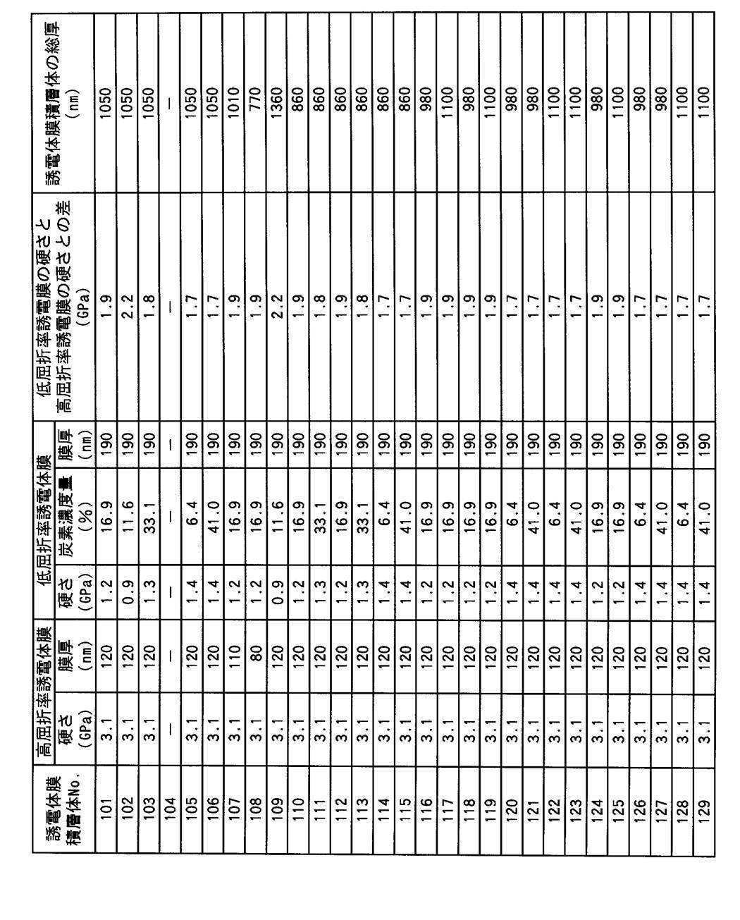
評価
作製した各誘電体膜積層体No.101から129に付き、クラック耐性、ヘーズ、遮熱性を以下に示す方法で試験し、以下に示す評価ランクに従って評価した結果を表3に示す。
作製した各誘電体膜積層体No.101から129に付き、クラック耐性、ヘーズ、遮熱性を以下に示す方法で試験し、以下に示す評価ランクに従って評価した結果を表3に示す。
クラック耐性の試験方法
作製した試料を100倍ルーペを用いて目視観察した。
作製した試料を100倍ルーペを用いて目視観察した。
クラック耐性の評価ランク
5:クラック発生なし
4:クラック若干発生あるが、使用上問題なし
3:クラック発生あるが、使用上懸念
2:クラック発生あり、使用上問題あり
1:クラック発生あり、使用出来ない
ヘーズの試験方法
作製した試料を、日本電色工業株式会社 NDH 2000を用いて光源D65 JIS 7361-1に基づいて測定した。数値が大きいほどヘーズ値が高く、可視性が悪くなり、低いほど可視性が良好となる。
5:クラック発生なし
4:クラック若干発生あるが、使用上問題なし
3:クラック発生あるが、使用上懸念
2:クラック発生あり、使用上問題あり
1:クラック発生あり、使用出来ない
ヘーズの試験方法
作製した試料を、日本電色工業株式会社 NDH 2000を用いて光源D65 JIS 7361-1に基づいて測定した。数値が大きいほどヘーズ値が高く、可視性が悪くなり、低いほど可視性が良好となる。
〔遮熱性の評価〕
誘電体積層体の片面を赤外線照射器(日本ピー・アイ(株))で赤外線ランプ1000ワット、距離150mmから照射し、裏面から50mm離れた位置の温度を非接触温度計(株式会社シロ産業 製 MB8R-303K)で測定し、誘電体積層体を使用しなかった時の温度に対する温度差を遮熱性とした。温度差が大きい程、遮熱性に優れていることを示す。
誘電体積層体の片面を赤外線照射器(日本ピー・アイ(株))で赤外線ランプ1000ワット、距離150mmから照射し、裏面から50mm離れた位置の温度を非接触温度計(株式会社シロ産業 製 MB8R-303K)で測定し、誘電体積層体を使用しなかった時の温度に対する温度差を遮熱性とした。温度差が大きい程、遮熱性に優れていることを示す。
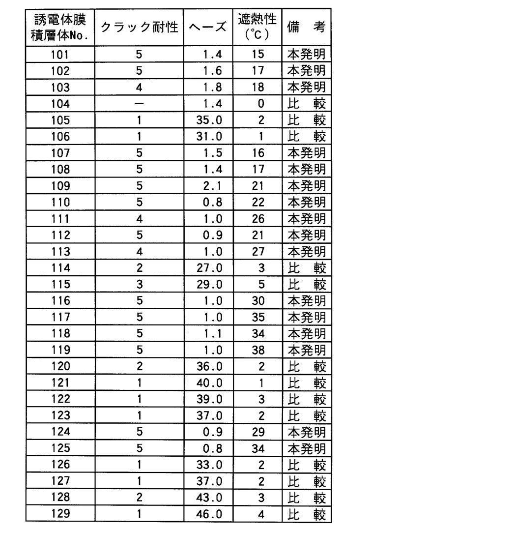
本発明の基材の上に、低屈折率誘電体膜と、高屈折率誘電体膜とが交互に積層された本発明の誘電体膜積層体はクラック耐性、ヘーズ、遮熱性共に優れた性能が得られることを確認した。本発明の有効性が確認された。
実施例2
(誘電体膜積層体No.201の作製)
放電ガス窒素、薄膜形成ガス、添加ガスの体積%を変化させる事で、低屈折率誘電体膜の炭素濃度量V=6.5を作成した以外実施例1で作成した誘電体膜積層体No.105と同様の誘電体膜積層体を作成しNo.201とした。
(誘電体膜積層体No.201の作製)
放電ガス窒素、薄膜形成ガス、添加ガスの体積%を変化させる事で、低屈折率誘電体膜の炭素濃度量V=6.5を作成した以外実施例1で作成した誘電体膜積層体No.105と同様の誘電体膜積層体を作成しNo.201とした。
(誘電体膜積層体No.202の作製)
放電ガス窒素、薄膜形成ガス、添加ガスの体積%を変化させる事で、低屈折率誘電体膜の炭素濃度量V40.0を作成した以外実施例1で作成した誘電体膜積層体No.105と同様の誘電体膜積層体を作成しNo.202とした。
放電ガス窒素、薄膜形成ガス、添加ガスの体積%を変化させる事で、低屈折率誘電体膜の炭素濃度量V40.0を作成した以外実施例1で作成した誘電体膜積層体No.105と同様の誘電体膜積層体を作成しNo.202とした。
この時のNo.201、No.202高屈折率誘電体膜との硬さの差は1.4GPaから3.0GPa範囲であった。
評価
作製した誘電体膜積層体No.201、202に付き、クラック耐性、ヘーズ、遮熱性を実施例1と同じ方法で試験した結果、誘電体膜積層体No.201はクラック耐性4、ヘーズ2.1、遮熱性10であった。誘電体膜積層体No.202はクラック耐性3、ヘーズ2.7、遮熱性11であった。
作製した誘電体膜積層体No.201、202に付き、クラック耐性、ヘーズ、遮熱性を実施例1と同じ方法で試験した結果、誘電体膜積層体No.201はクラック耐性4、ヘーズ2.1、遮熱性10であった。誘電体膜積層体No.202はクラック耐性3、ヘーズ2.7、遮熱性11であった。
実施例3
片面7層で、各層の厚さが下記に示す厚さを有し、総厚545nmにした以外は実施例1で作製した誘電体膜積層体No.101と同じ方法で誘電体膜積層体を作成した。
片面7層で、各層の厚さが下記に示す厚さを有し、総厚545nmにした以外は実施例1で作製した誘電体膜積層体No.101と同じ方法で誘電体膜積層体を作成した。
層構成と各層の厚さ
支持体/高屈折率層(120nm)/低屈折率層(65nm)/高屈折率層(120nm)/低屈折率層(65nm)/高屈折率層(100nm)/低屈折率層(65nm)/高屈折率層(10nm)
評価
作製した誘電体膜積層体に付き、クラック耐性、ヘーズ、遮熱性を実施例1と同じ方法で試験した結果、クラック耐性5、ヘーズ10、遮熱性9であった。
支持体/高屈折率層(120nm)/低屈折率層(65nm)/高屈折率層(120nm)/低屈折率層(65nm)/高屈折率層(100nm)/低屈折率層(65nm)/高屈折率層(10nm)
評価
作製した誘電体膜積層体に付き、クラック耐性、ヘーズ、遮熱性を実施例1と同じ方法で試験した結果、クラック耐性5、ヘーズ10、遮熱性9であった。
1 誘電体膜積層体
101、F 基材
102 誘電体膜積層膜
102a 高屈折率誘電体膜
102b 低屈折率誘電体膜
A、B プラズマ放電処理装置
11 第1電極
12 第2電極
21 第1電源
22 第2電源
13、33 対向電極間(放電空間)
31 ロール回転電極(第1電極)
31A、32A 金属質母材
31B、32B 誘電体
32 固定電極群(第2電極)
40 電界印加手段
41 第1電源
42 第2電源
50 ガス供給手段
51 ガス発生装置
52 給気口
53 排気口
60 電極温度調節手段
G 薄膜形成ガス
G° プラズマ状態のガス
G′ 処理排ガス
101、F 基材
102 誘電体膜積層膜
102a 高屈折率誘電体膜
102b 低屈折率誘電体膜
A、B プラズマ放電処理装置
11 第1電極
12 第2電極
21 第1電源
22 第2電源
13、33 対向電極間(放電空間)
31 ロール回転電極(第1電極)
31A、32A 金属質母材
31B、32B 誘電体
32 固定電極群(第2電極)
40 電界印加手段
41 第1電源
42 第2電源
50 ガス供給手段
51 ガス発生装置
52 給気口
53 排気口
60 電極温度調節手段
G 薄膜形成ガス
G° プラズマ状態のガス
G′ 処理排ガス
Claims (8)
- 基材の上に、低屈折率誘電体膜と、高屈折率誘電体膜とが交互に積層された誘電体膜積層膜を有する誘電体膜積層体において、前記低屈折率誘電体膜と、前記高屈折率誘電体膜との硬さが異なり、前記低屈折率誘電体膜の炭素濃度量をVとすると、6.5≦V≦40.0であることを特徴とする誘電体膜積層体。
- 前記低屈折率誘電体膜と高屈折率誘電体膜とのナノインデンテーション法で測定した硬さの差が、1.4GPaから3.0GPaであることを特徴とする請求項1に記載の誘電体膜積層体。
- 前記誘電体膜積層膜が基材の片面、又は両面に設けられていることを特徴とする請求項1又は2に記載の誘電体膜積層体。
- 前記誘電体膜積層膜の総厚が、500nm以上であることを特徴とする請求項1から3の何れか1項に記載の誘電体膜積層体。
- 前記低屈折率誘電体膜と高屈折率誘電体膜とが赤外線反射膜であることを特徴とする請求項1から4の何れか1項に記載の誘電体膜積層体。
- 基材上に、硬さの異なる低屈折率誘電体膜と高屈折率誘電体膜が交互に積層された誘電体膜積層膜を有する誘電体膜積層体の製造方法において、前記低屈折率誘電体膜及び前記高屈折率誘電体膜は、大気圧又は大気近傍の圧力下で、ガスを放電空間に導入し、該放電空間に高周波電界を形成することによりガスをプラズマ状態とし、前記基材を前記プラズマ状態のガスに晒すことによって形成されたことを特徴とする誘電体膜積層体の製造方法。
- 前記低屈折率誘電体膜と前記高屈折率誘電体膜とのナノインデンテーション法で測定した硬さの差が、1.4GPaから3.0GPaであることを特徴とする請求項6に記載の誘電体膜積層体の製造方法。
- 前記誘電体膜積層膜の総厚が、500nm以上であることを特徴とする請求項6又は7に記載の誘電体膜積層体の製造方法。
Priority Applications (1)
| Application Number | Priority Date | Filing Date | Title |
|---|---|---|---|
| JP2011504785A JPWO2010106866A1 (ja) | 2009-03-18 | 2010-02-18 | 誘電体膜積層体、誘電体膜積層体の製造方法 |
Applications Claiming Priority (4)
| Application Number | Priority Date | Filing Date | Title |
|---|---|---|---|
| JP2009-066193 | 2009-03-18 | ||
| JP2009066193 | 2009-03-18 | ||
| JP2009-143144 | 2009-06-16 | ||
| JP2009143144 | 2009-06-16 |
Publications (1)
| Publication Number | Publication Date |
|---|---|
| WO2010106866A1 true WO2010106866A1 (ja) | 2010-09-23 |
Family
ID=42739532
Family Applications (1)
| Application Number | Title | Priority Date | Filing Date |
|---|---|---|---|
| PCT/JP2010/052421 Ceased WO2010106866A1 (ja) | 2009-03-18 | 2010-02-18 | 誘電体膜積層体、誘電体膜積層体の製造方法 |
Country Status (2)
| Country | Link |
|---|---|
| JP (1) | JPWO2010106866A1 (ja) |
| WO (1) | WO2010106866A1 (ja) |
Cited By (2)
| Publication number | Priority date | Publication date | Assignee | Title |
|---|---|---|---|---|
| WO2014188831A1 (ja) * | 2013-05-22 | 2014-11-27 | コニカミノルタ株式会社 | 紫外線遮蔽フィルム |
| JP2017220411A (ja) * | 2016-06-10 | 2017-12-14 | 日東電工株式会社 | 透明導電性フィルム |
Citations (4)
| Publication number | Priority date | Publication date | Assignee | Title |
|---|---|---|---|---|
| JPH0872193A (ja) * | 1994-09-08 | 1996-03-19 | Toppan Printing Co Ltd | 透明性を有するガスバリア性積層フィルム |
| JP2000338307A (ja) * | 1999-05-28 | 2000-12-08 | Dainippon Printing Co Ltd | 反射防止フィルム |
| JP2003294901A (ja) * | 2002-03-29 | 2003-10-15 | Konica Corp | 反射防止フィルム、低屈折率領域の作製方法、偏光板 |
| JP2005292462A (ja) * | 2004-03-31 | 2005-10-20 | Konica Minolta Opto Inc | 誘電体多層膜を有する光学素子 |
-
2010
- 2010-02-18 JP JP2011504785A patent/JPWO2010106866A1/ja active Pending
- 2010-02-18 WO PCT/JP2010/052421 patent/WO2010106866A1/ja not_active Ceased
Patent Citations (4)
| Publication number | Priority date | Publication date | Assignee | Title |
|---|---|---|---|---|
| JPH0872193A (ja) * | 1994-09-08 | 1996-03-19 | Toppan Printing Co Ltd | 透明性を有するガスバリア性積層フィルム |
| JP2000338307A (ja) * | 1999-05-28 | 2000-12-08 | Dainippon Printing Co Ltd | 反射防止フィルム |
| JP2003294901A (ja) * | 2002-03-29 | 2003-10-15 | Konica Corp | 反射防止フィルム、低屈折率領域の作製方法、偏光板 |
| JP2005292462A (ja) * | 2004-03-31 | 2005-10-20 | Konica Minolta Opto Inc | 誘電体多層膜を有する光学素子 |
Cited By (2)
| Publication number | Priority date | Publication date | Assignee | Title |
|---|---|---|---|---|
| WO2014188831A1 (ja) * | 2013-05-22 | 2014-11-27 | コニカミノルタ株式会社 | 紫外線遮蔽フィルム |
| JP2017220411A (ja) * | 2016-06-10 | 2017-12-14 | 日東電工株式会社 | 透明導電性フィルム |
Also Published As
| Publication number | Publication date |
|---|---|
| JPWO2010106866A1 (ja) | 2012-09-20 |
Similar Documents
| Publication | Publication Date | Title |
|---|---|---|
| JP4821610B2 (ja) | 透明ガスバリア性フィルム | |
| KR20020089344A (ko) | 박막 형성 방법, 박막을 갖는 물품, 광학 필름, 유전체피복 전극 및 플라즈마 방전 처리 장치 | |
| JPWO2008096617A1 (ja) | 透明ガスバリア性フィルム及び透明ガスバリア性フィルムの製造方法 | |
| JP2013063658A (ja) | ガスバリア積層体の製造方法及びガスバリア積層体 | |
| JP2006068992A (ja) | ガスバリア性フィルム | |
| JPWO2006033268A1 (ja) | 透明導電膜 | |
| JP2008062460A (ja) | 光学フィルムとそれを用いた画像表示素子 | |
| JP4014357B2 (ja) | 撥水性防汚フィルム | |
| WO2010106866A1 (ja) | 誘電体膜積層体、誘電体膜積層体の製造方法 | |
| JP2011036778A (ja) | バリアフィルムの製造方法 | |
| JP5012745B2 (ja) | ハードコート層付積層体 | |
| WO2009131136A1 (ja) | 遮熱樹脂基材またこれを用いた建築部材 | |
| JP2004269772A (ja) | 光学フィルム、その製造方法及びその光学フィルムを用いた表示装置 | |
| JP2011036803A (ja) | バリアフィルムの製造方法 | |
| WO2010095479A1 (ja) | 誘電体積層体、合わせガラス、誘電体積層体の製造方法及び合わせガラスの製造方法 | |
| WO2009147928A1 (ja) | 遮熱樹脂フィルムおよびこれを貼り合わせた建築部材 | |
| JP2009279778A (ja) | ハードコート層付積層体 | |
| JP2007017668A (ja) | 光学フィルム | |
| JP2011104830A (ja) | 誘電体膜積層体及び誘電体膜積層体の製造方法 | |
| JP5482651B2 (ja) | ハードコート層付積層体 | |
| WO2006075490A1 (ja) | 透明ガスバリアフィルム | |
| JP2003294945A (ja) | 光学フィルム及びその製造方法、それを用いた偏光板、表示装置 | |
| JP2008132643A (ja) | 液晶セル用基板、液晶表示装置 | |
| US20140255288A1 (en) | Gas barrier laminate and production method of the same | |
| JP2004347778A (ja) | 光学フィルム、偏光板およびそれを用いた液晶表示装置 |
Legal Events
| Date | Code | Title | Description |
|---|---|---|---|
| 121 | Ep: the epo has been informed by wipo that ep was designated in this application |
Ref document number: 10753361 Country of ref document: EP Kind code of ref document: A1 |
|
| WWE | Wipo information: entry into national phase |
Ref document number: 2011504785 Country of ref document: JP |
|
| NENP | Non-entry into the national phase |
Ref country code: DE |
|
| 122 | Ep: pct application non-entry in european phase |
Ref document number: 10753361 Country of ref document: EP Kind code of ref document: A1 |