WO2010106843A1 - 基板処理方法および基板処理装置 - Google Patents
基板処理方法および基板処理装置 Download PDFInfo
- Publication number
- WO2010106843A1 WO2010106843A1 PCT/JP2010/051597 JP2010051597W WO2010106843A1 WO 2010106843 A1 WO2010106843 A1 WO 2010106843A1 JP 2010051597 W JP2010051597 W JP 2010051597W WO 2010106843 A1 WO2010106843 A1 WO 2010106843A1
- Authority
- WO
- WIPO (PCT)
- Prior art keywords
- substrate
- temperature
- gas
- processing
- organic acid
- Prior art date
- Legal status (The legal status is an assumption and is not a legal conclusion. Google has not performed a legal analysis and makes no representation as to the accuracy of the status listed.)
- Ceased
Links
Images


Classifications
-
- H—ELECTRICITY
- H10—SEMICONDUCTOR DEVICES; ELECTRIC SOLID-STATE DEVICES NOT OTHERWISE PROVIDED FOR
- H10P—GENERIC PROCESSES OR APPARATUS FOR THE MANUFACTURE OR TREATMENT OF DEVICES COVERED BY CLASS H10
- H10P50/00—Etching of wafers, substrates or parts of devices
-
- H—ELECTRICITY
- H10—SEMICONDUCTOR DEVICES; ELECTRIC SOLID-STATE DEVICES NOT OTHERWISE PROVIDED FOR
- H10P—GENERIC PROCESSES OR APPARATUS FOR THE MANUFACTURE OR TREATMENT OF DEVICES COVERED BY CLASS H10
- H10P70/00—Cleaning of wafers, substrates or parts of devices
- H10P70/20—Cleaning during device manufacture
- H10P70/23—Cleaning during device manufacture during, before or after processing of insulating materials
- H10P70/234—Cleaning during device manufacture during, before or after processing of insulating materials the processing being the formation of vias or contact holes
-
- H—ELECTRICITY
- H10—SEMICONDUCTOR DEVICES; ELECTRIC SOLID-STATE DEVICES NOT OTHERWISE PROVIDED FOR
- H10W—GENERIC PACKAGES, INTERCONNECTIONS, CONNECTORS OR OTHER CONSTRUCTIONAL DETAILS OF DEVICES COVERED BY CLASS H10
- H10W20/00—Interconnections in chips, wafers or substrates
- H10W20/01—Manufacture or treatment
-
- H—ELECTRICITY
- H10—SEMICONDUCTOR DEVICES; ELECTRIC SOLID-STATE DEVICES NOT OTHERWISE PROVIDED FOR
- H10W—GENERIC PACKAGES, INTERCONNECTIONS, CONNECTORS OR OTHER CONSTRUCTIONAL DETAILS OF DEVICES COVERED BY CLASS H10
- H10W20/00—Interconnections in chips, wafers or substrates
- H10W20/01—Manufacture or treatment
- H10W20/071—Manufacture or treatment of dielectric parts thereof
- H10W20/081—Manufacture or treatment of dielectric parts thereof by forming openings in the dielectric parts
-
- H—ELECTRICITY
- H10—SEMICONDUCTOR DEVICES; ELECTRIC SOLID-STATE DEVICES NOT OTHERWISE PROVIDED FOR
- H10W—GENERIC PACKAGES, INTERCONNECTIONS, CONNECTORS OR OTHER CONSTRUCTIONAL DETAILS OF DEVICES COVERED BY CLASS H10
- H10W20/00—Interconnections in chips, wafers or substrates
- H10W20/01—Manufacture or treatment
- H10W20/031—Manufacture or treatment of conductive parts of the interconnections
- H10W20/056—Manufacture or treatment of conductive parts of the interconnections by filling conductive material into holes, grooves or trenches
Definitions
- the present invention relates to a substrate processing method and a substrate processing apparatus for removing Cu-containing residue adhering to an oxide on a Cu film surface and an interlayer insulating film when forming a Cu wiring.
- Cu copper
- Al aluminum
- W tungsten
- Cu has a problem that it is easily oxidized and copper oxide with high resistance is easily formed on its surface, making it difficult to make a contact. Therefore, it is necessary to remove the oxide film formed on the Cu surface.
- a part of the lower layer Cu wiring exposed at the bottom of the wiring trench or via is etched when the interlayer insulating film is etched.
- Cu-containing materials adhere to the side walls of the grooves and vias as residues. If the next step is performed with such a residue attached, Cu diffuses into the interlayer insulating film and reduces the yield of the semiconductor device. Therefore, it is necessary to remove such a Cu-containing residue.
- wet cleaning has been used as a method for removing Cu-containing residue adhering to the interlayer insulating film.
- a low-k film is used as the interlayer insulating film, the low-k film absorbs moisture by the wet cleaning. Therefore, a method of removing such Cu-containing residues using organic acid dry cleaning (for example, Enhancing Yield and Reliability by Applying Dry Organic Acid Vapor Cleaning to Copper Contact Via-Bottom for 32-nm Nodes and Beyond (International Interconnect Technology Conference, 2008. p93-p95) is under consideration.
- An object of the present invention is to provide a substrate processing method and a substrate processing apparatus capable of efficiently and reliably removing copper oxide on the Cu surface and removing Cu-containing residue adhered to an interlayer insulating film.
- Another object of the present invention is to provide a storage medium storing a program for executing such a substrate processing method.
- the present inventor tends to etch at a low temperature and to reduce at a high temperature when dry cleaning using an organic acid-containing gas is performed on copper oxide. I found out.
- the following points were conceived. That is, the Cu-containing residue adhering to the interlayer insulating film in the Cu wiring structure is thought to be mainly composed of copper oxide, and such Cu-containing residue needs to be removed by etching, so that etching is likely to occur at a low temperature. Remove by dry cleaning with organic acid containing gas.
- the copper oxide film may be removed by either etching removal or reduction removal, but the reaction at low temperature has a slow reaction rate and takes time.
- the reaction rate is high at a high temperature, the copper oxide film on the Cu surface can be reliably removed in a short time by causing a reaction mainly composed of reduction at a high temperature at which the reaction occurs at a higher speed.
- the present invention has been completed based on such knowledge.
- a substrate processing method for removing a Cu-containing residue adhering to a copper oxide film and an interlayer insulating film on a Cu surface in a Cu wiring structure on a substrate using an organic acid-containing gas.
- the substrate processing method including the process of removing by this is provided.
- the present invention is suitable when the interlayer insulating film is a low-k film.
- the organic acid is preferably a carboxylic acid, and formic acid is particularly preferable.
- the first temperature is 100 to 200 ° C. and the second temperature is 200 to 300 ° C.
- a substrate processing apparatus for removing a Cu-containing residue adhering to a copper oxide film and an interlayer insulating film on a Cu surface in a Cu wiring structure on a substrate using an organic acid-containing gas.
- a gas supply mechanism, an exhaust mechanism for exhausting the inside of the chamber, and the substrate is placed on the mounting table, and the substrate is organically heated while the substrate is heated to a first relatively low temperature by the heating mechanism.
- a process gas containing an acid gas is supplied to perform etching removal of Cu-containing residue, and then the temperature of the substrate is raised to a second temperature higher than the first temperature by the heating mechanism, Organic acid gas on the substrate A substrate processing apparatus and a control mechanism for controlling the copper oxide film of the Cu surface by supplying the untreated gas so as to remove by reaction which is mainly reduction is provided.
- a substrate processing apparatus for removing a Cu-containing residue adhering to a copper oxide film and an interlayer insulating film on a Cu surface in a Cu wiring structure on a substrate using an organic acid-containing gas.
- a chamber for accommodating the substrate, a mounting table for mounting the substrate in the chamber, a heating mechanism for heating the substrate on the mounting table, and an energy medium gas heated to the substrate on the mounting table An energy medium gas supply mechanism, a processing gas for supplying a processing gas containing an organic acid gas into the chamber, an exhaust mechanism for exhausting the chamber, and a substrate placed on the mounting table, While the substrate is heated to a relatively low first temperature by a heating mechanism, a processing gas containing an organic acid gas is supplied to the substrate to remove the Cu-containing residue, and then the substrate on the mounting table In A heated energy medium gas is supplied to raise the temperature of the substrate to a second temperature higher than the first temperature, and then a processing gas containing an organic acid gas is supplied to the substrate to increase the temperature of the Cu surface.
- a substrate processing apparatus including a control mechanism for controlling a copper oxide film to be removed by a reaction mainly including reduction.
- a substrate processing apparatus for removing a Cu-containing residue adhering to a copper oxide film and an interlayer insulating film on a Cu surface in a Cu wiring structure on a substrate using an organic acid-containing gas.
- a first processing unit having a mounting table that is held at a temperature at which the mounted substrate can be heated to the first temperature, and capable of supplying the processing gas to the substrate on the mounting table
- a second processing unit having a mounting table that is maintained at a temperature at which the placed substrate can be heated to the second temperature, and capable of supplying a processing gas to the substrate on the mounting table; The substrate is placed on the placing table of the first processing unit, and the substrate is heated to the first temperature while the substrate is heated to the first temperature.
- a processing gas containing an organic acid gas is supplied to perform etching removal of Cu-containing residue,
- the substrate is transported to the mounting table of the second processing unit by the feeding mechanism, and a processing gas containing an organic acid gas is supplied to the substrate while heating the substrate to the second temperature, and the copper oxide film on the Cu surface is formed.
- a substrate processing apparatus including a control mechanism that controls to be removed by a reaction mainly composed of reduction.
- a substrate processing apparatus for removing a Cu-containing residue adhering to a copper oxide film and an interlayer insulating film on a Cu surface in a Cu wiring structure on a substrate using an organic acid-containing gas.
- a processing container for processing the substrate a substrate holding unit for holding a plurality of substrates in the processing container, a heating mechanism for heating the plurality of substrates in the processing container, and an organic acid gas in the processing container.
- a processing gas supply mechanism for supplying a processing gas containing the substrate, and the substrate holding portion in a state where a plurality of substrates are held in the processing container;
- a processing gas containing an organic acid gas is supplied to the plurality of substrates while being heated to the first temperature, so that the Cu-containing residue is removed by etching, and then the temperatures of the plurality of substrates are adjusted by the heating mechanism.
- a substrate processing apparatus is provided.
- a storage medium that operates on a computer and stores a program for controlling a substrate processing apparatus, and the program is stored in a Cu wiring structure on a substrate at the time of execution.
- a substrate processing method including a step of supplying a processing gas containing an organic acid gas to the substrate while heating the substrate and removing the copper oxide film on the Cu surface by a reaction mainly comprising reduction; in front Storage medium for controlling a substrate processing apparatus is provided.
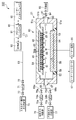
- FIG. 1 is a cross-sectional view schematically showing an example of a substrate processing apparatus used for carrying out the substrate processing method according to the first embodiment of the present invention.
- a substrate processing apparatus used for carrying out the substrate processing method according to the first embodiment of the present invention.
- a semiconductor wafer hereinafter simply referred to as a wafer
- the substrate will be described (the same applies to the following embodiments).
- the processing apparatus 100 has a substantially cylindrical chamber 1 that is airtight. On the bottom wall of the chamber 1, a mounting table 3 for horizontally supporting a wafer W, which is a semiconductor substrate, is provided in the chamber 1.
- a heater 4 is embedded in the mounting table 3, and a heater power source 5 is connected to the heater 4.
- a thermocouple 6 is provided in the vicinity of the upper surface of the mounting table 3, and a signal from the thermocouple 6 is transmitted to the heater controller 7.
- the heater controller 7 transmits a command to the heater power source 5 in accordance with a signal from the thermocouple 6 and controls the heating of the heater 4 to control the wafer W to a predetermined temperature.
- three wafer support pins are provided so as to protrude and retract with respect to the surface of the mounting table 3 in order to support the wafer W and move it up and down.
- a shower head 10 is provided on the top wall 1 a of the chamber 1.
- a gas introduction port 12 for introducing gas into the shower head 10 is provided on the upper surface of the shower head 10, and a pipe 21 for supplying a cleaning gas and a purge gas is connected to the gas introduction port 12. ing.
- a diffusion chamber 14 is formed inside the shower head 10, and a plurality of discharge holes 11 for discharging a processing gas and a purge gas toward the mounting table 3 are formed on the lower surface of the shower head 10. Then, the gas introduced into the shower head 10 from the gas inlet 12 is diffused in the diffusion chamber 14 and discharged perpendicularly to the wafer W mounted on the mounting table 3 in the chamber 1 from the discharge hole 11.
- a processing gas supply source 22 for supplying a processing gas is connected to the other end of the pipe 21 connected to the gas inlet 12.
- the pipe 21 is provided with a mass flow controller 23 and front and rear valves 24.
- An inert gas pipe 25 is connected to the pipe 21, and an inert gas supply source 26 is connected to the other end of the inert gas pipe 25.
- the inert gas pipe 25 is provided with a mass flow controller 27 and front and rear valves 28.
- the processing gas supplied from the processing gas supply source 22 one containing an organic acid gas is used.
- carboxylic acid can be preferably used.
- carboxylic acid formic acid (HCOOH), acetic acid (CH 3 COOH), propionic acid (CH 3 CH 2 COOH), butyric acid (CH 3 (CH 2 ) 2 COOH), valeric acid (CH 3 (CH 2 ) 3 COOH) Among these, formic acid (HCOOH) is preferable.
- the inert gas supplied from the inert gas supply source 26 is used as a purge gas, a dilution gas, a carrier gas, and the like, and examples thereof include Ar gas, He gas, and N 2 gas.
- An exhaust port 31 is formed in the bottom wall 1 b of the chamber 1, and an exhaust pipe 32 is connected to the exhaust port 31.
- the exhaust pipe 32 is provided with an exhaust device 33 including a high-speed vacuum pump.
- the exhaust pipe 32 is provided with a conductance variable valve 34 so that the exhaust amount from the chamber 1 can be adjusted.
- a loading / unloading port 15 for loading / unloading the wafer W to / from a transfer chamber (not shown) adjacent to the substrate processing apparatus 100, and a gate valve 16 for opening / closing the loading / unloading port. Is provided.
- the substrate processing apparatus 100 includes a control unit 40, and the control unit 40 includes a process controller 41, a user interface 42, and a storage unit 43.
- Each component of the substrate processing apparatus 100 such as a valve, a mass flow controller, a heater controller 7, and an exhaust device 33, is connected to the process controller 41, and these are controlled by the process controller 41.
- the user interface 42 is connected to the process controller 41, and includes a keyboard on which an operator inputs commands to manage the processing apparatus, a display that visualizes and displays the operating status of the plasma processing apparatus, and the like.
- the storage unit 43 is connected to the process controller 41, and the control program for realizing various processes executed by the substrate processing apparatus 100 under the control of the process controller 41 and the processing conditions of the substrate processing apparatus 100.
- a program for causing each component to execute processing, that is, a processing recipe is stored.
- the processing recipe is stored in a storage medium in the storage unit 43.
- the storage medium may be a fixed medium such as a hard disk or a portable medium such as a CDROM, DVD, or flash memory. Moreover, you may make it transmit a recipe suitably from another apparatus via a dedicated line, for example.
- an arbitrary processing recipe is called from the storage unit 43 by an instruction from the user interface 42 and is executed by the process controller 41, so that the substrate processing apparatus 100 can control the process controller 41.
- a cleaning process is performed.
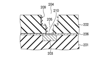
- a low-k film 202 which is an upper interlayer insulating film, is formed on a low-k film 201, which is a lower interlayer insulating film, via a cap film 206.
- a position corresponding to the Cu wiring layer 203 of the Low-k film 202 is plasma-etched on the wafer W having the Cu wiring layer 203 formed on the Low-k film 201 to form a trench 204 and a hole 205, and the resist is ashed.
- the Cu-containing residue 209 adhering to the sidewalls of the trench 204 and the hole 205 and the copper oxide film 210 formed on the surface of the Cu wiring layer 203 are removed by dry cleaning with a processing gas containing an organic acid gas. .
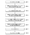
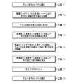
- the gate valve 16 is opened and the wafer W having the Cu wiring structure is loaded into the chamber 1 from the loading / unloading port 15 and mounted on the mounting table 3 (step 1). ).
- the gate valve 16 is closed, and based on the temperature detection signal from the thermocouple 6, the heater 4 is controlled by the heater controller 7 to change the temperature of the wafer W to the etching reaction of copper oxide, which is the main component of the Cu-containing residue 209. Control is performed to a relatively low first temperature that becomes dominant (step 2).
- Step 3 the valve 28 is opened, for example, Ar gas is introduced from the inert gas supply source 26, and the temperature of the wafer W is stabilized at the first temperature.
- step 4 a processing gas containing an organic acid gas is supplied from the processing gas supply source 22 into the chamber 1 through the shower head 10 while controlling the flow rate by the mass flow controller 23, and mainly contains Cu-containing residue. 209 is removed by etching (step 4). This step is performed until the Cu-containing residue 209 is almost completely removed by etching. At this time, a part of the copper oxide film 210 is also removed by etching.
- the organic acid constituting the processing gas formic acid (HCOOH), acetic acid (CH 3 COOH), propionic acid (CH 3 CH 2 COOH), butyric acid (CH 3 (CH 2 ) 2 COOH), Carboxylic acids such as herbic acid (CH 3 (CH 2 ) 3 COOH) can be suitably used, and among these, formic acid (HCOOH) is preferred.
- the first temperature at this time is preferably in the range of 100 to 200 ° C., for example, when the organic acid used is a carboxylic acid such as formic acid (HCOOH).
- the etching reaction when formic acid is used as the organic acid can be expressed by the following formula (1).
- processing gas may be supplied immediately after the wafer W is placed on the placement table 3 without performing the stabilization step of Step 3. Further, in step 4, the inert gas may be stopped even in a state where it is allowed to flow.
- step 4 After the Cu-containing residue 209 is almost completely removed by the process of step 4, the supply of the process gas is stopped, and the heater controller 7 supplies the inert gas while the heater controller 7 generates a heater based on the temperature detection signal from the thermocouple 6. 4 is controlled to control the temperature of the wafer W to a second temperature higher than the first temperature at which the reduction of copper oxide is dominant (step 5).
- the processing gas containing the organic acid gas is again supplied from the processing gas supply source 22 into the chamber 1 through the shower head 10 while controlling the flow rate by the mass flow controller 23, and the surface of the Cu wiring layer 203.
- the copper oxide film 210 is removed by a reaction mainly composed of a reduction reaction (step 6).
- the second temperature at this time is preferably in the range of 200 to 300 ° C., for example, when the organic acid to be used is a carboxylic acid such as formic acid (HCOOH).
- the reduction reaction when formic acid is used as the organic acid can be represented by the following formula (2).
- the processing gas may be supplied before the temperature stabilizes, or may be performed while flowing the processing gas when the temperature is changed after step 4. However, the flow rate of the processing gas when the temperature is lower than the second temperature increases the rate at which the copper oxide film is removed by etching.
- the removal process by the reaction mainly including the reduction of the copper oxide film 210 is continued until the copper oxide film 210 is completely removed.
- the supply of the processing gas is stopped, and the chamber is passed through the shower head 10 while the flow rate is controlled by the mass flow controller 27 using the inert gas as the purge gas from the inert gas supply source 26. 1 is supplied to purge the inside of the chamber 1 (step 7).
- the gate valve 16 is opened and the wafer W is unloaded from the loading / unloading port 15 (step 8).
- the temperature is changed between the removal of the Cu-containing residue 209 and the removal of the copper oxide film 210 for the following reason.
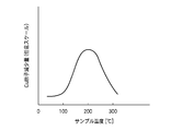
- FIG. 4 shows a sample in which a Cu 2 O film having a thickness of 300 nm is formed on a Si substrate.
- the sample temperature is increased while formic acid (HCOOH) gas is supplied to the sample.
- HCOOH formic acid
- the relationship obtained by the Cu—K ⁇ ray detection intensity measured with fluorescent X-rays is shown.
- the amount of reduction of Cu atoms increases at low temperatures, the amount of reduction of Cu atoms becomes maximum near 200 ° C., and the amount of reduction of Cu atoms decreases at higher temperatures. Recognize. From this figure, it can be seen that Cu 2 O etching is dominant at temperatures lower than 200 ° C. and Cu 2 O reduction is dominant at temperatures higher than 200 ° C.
- the Cu-containing residue 209 that needs to be removed by etching is dry-cleaned with an organic acid-containing gas at a relatively low first temperature, for example, 100 to 200 ° C., where the etching reaction is dominant. Can be removed in a relatively short time.
- the removal of the copper oxide film may be either etching removal or reduction removal, but generally the reaction rate is slow at low temperatures and the reaction at high temperatures. Since the speed is high, the copper oxide film 210 is reliably removed in a shorter time by generating a reaction mainly composed of reduction at a second temperature at which a reaction with a higher reaction speed occurs, for example, 200 to 300 ° C. be able to.
- the Cu-containing residue 209 and the copper oxide film 210 when removing the Cu-containing residue 209 and the copper oxide film 210 by dry cleaning with an organic acid-containing gas, the Cu-containing residue is removed by etching at a first temperature that is relatively low.
- the copper oxide on the surface of Cu by a reaction mainly composed of reduction at a second temperature higher than the first temperature, these can be reliably removed in a short time.
- the substrate processing apparatus 100 forms a unit for forming a barrier film such as a Ta film, a Ti film, or a Ru film and a subsequent Cu seed film for forming Cu wiring in the trench 204 and the via 205.
- a cluster tool type multi-chamber system having a unit to perform the removal of the Cu-containing residue 209 and the copper oxide film 210, the formation of the barrier film, and the formation of the Cu seed film can be performed in-situ.
- This system is equipped with a unit for etching the low-k film and resist ashing so that a series of steps from the etching of the low-k film to the formation of the Cu seed film are performed in-situ. Also good.
- FIG. 5 is a cross-sectional view schematically showing an example of a substrate processing apparatus used for carrying out the substrate processing method according to the second embodiment of the present invention.
- the processing apparatus 200 has a substantially cylindrical chamber 51 that is airtight.
- a circular opening 52 is formed at the center of the bottom wall 51 a of the chamber 51, and a mounting table 53 for horizontally supporting the wafer W as a semiconductor substrate in the chamber 51 is formed in the opening 52. Is provided.
- a heat insulating part 58 is provided between the mounting table 53 and the bottom wall 51 a, and the heat insulating part 58 is airtightly joined to the bottom wall 1 a of the chamber 1.
- a heater 54 is embedded in the mounting table 53, and a heater power supply 55 is connected to the heater 54.
- a thermocouple 56 is provided in the vicinity of the upper surface of the mounting table 53, and signals from the thermocouple 56 are transmitted to the heater controller 57.
- the heater controller 57 transmits a command to the heater power supply 55 in accordance with a signal from the thermocouple 56, and controls the heating of the heater 54 to control the wafer W to a predetermined temperature.
- three wafer support pins (not shown) are provided so as to protrude and retract with respect to the surface of the mounting table 53 in order to support the wafer W and move it up and down.
- a shower head 60 is provided on the top wall 51 c of the chamber 1.
- a gas inlet 62 for introducing gas into the shower head 60 is provided on the upper surface of the shower head 60, and a pipe 63 for supplying energy medium gas is connected to the gas inlet 62.
- a diffusion chamber 64 is formed inside the shower head 60, and a plurality of discharge holes 61 for discharging energy medium gas toward the mounting table 53 are formed on the lower surface of the shower head 60.
- the gas introduced into the shower head 60 from the gas inlet 62 is diffused in the diffusion chamber 64 and discharged perpendicularly to the wafer W mounted on the mounting table 53 in the chamber 51 from the discharge hole 61.
- a heater 65 that is a heating unit for heating the energy medium gas in the shower head 60 is provided around each discharge hole 61 of the shower head 60.
- a heat insulating portion 66 made of a material having low thermal conductivity, for example, heat resistant synthetic resin, quartz, ceramics, or the like is provided around the heater 65 to be insulated. Then, the energy medium gas passing inside the heater 65 is heated instantaneously and efficiently.
- An energy medium gas supply source 73 for supplying energy medium gas is connected to the other end of the pipe 63 connected to the gas inlet 62.
- the pipe 63 is provided with a mass flow controller 71 and front and rear valves 72.
- an inert gas such as He, Ar, Kr, Xe, or N 2 can be suitably used.
- An organic acid gas can also be used.
- a gas inlet 67 is provided on one side wall 51 b of the chamber 51, and a pipe 68 is connected to the gas inlet 67.
- the pipe 68 is branched into a pipe 68a and a pipe 68b, and a processing gas supply source 76 for performing a cleaning process is connected to an end of the pipe 68a.
- the pipe 68a is provided with a mass flow controller 74a and front and rear valves 75a.
- An inert gas supply source 77 for supplying an inert gas is connected to the end of the pipe 68b.
- the pipe 68b is provided with a mass flow controller 74b and front and rear valves 75b.
- a gas containing an organic acid gas is used as in the first embodiment, and a carboxylic acid can be suitably used as the organic acid.
- a carboxylic acid formic acid (HCOOH), acetic acid (CH 3 COOH), propionic acid (CH 3 CH 2 COOH), butyric acid (CH 3 (CH 2 ) 2 COOH), valeric acid (CH 3 (CH 2 ) 3 COOH) Among these, formic acid (HCOOH) is preferable.
- the inert gas supplied from the inert gas supply source 77 purges the processing gas remaining in the gas phase, the by-products in the gas phase generated by the reaction, and the energy medium gas containing a large amount of thermal energy.
- Ar gas, He gas, N 2 gas and the like can be used as purge gas, dilution gas, carrier gas and the like.
- An exhaust port 81 is formed on the side of the side wall 51b of the chamber 51 opposite to the gas introduction port 67, and an exhaust pipe 82 is connected to the exhaust port 81.
- the exhaust pipe 82 is provided with an exhaust device 83 including a high-speed vacuum pump.
- the exhaust pipe 82 is provided with a conductance variable valve 84 so that the exhaust amount from the chamber 51 can be adjusted.
- Loading of the wafer W into and from the transfer chamber (not shown) adjacent to the processing apparatus 200 is performed on the side wall of the chamber 51 where the gas introduction port 67 and the exhaust port 81 are not formed.
- An outlet and a gate valve that opens and closes the loading / unloading port are provided (both are not shown).
- the processing apparatus 200 includes a control unit 90, and the control unit 90 includes a process controller 91, a user interface 92, and a storage unit 93.
- the process controller 91, the user interface 92, and the storage unit 93 are configured in the same manner as the process controller 41, the user interface 42, and the storage unit 43 in the first embodiment.
- the Cu-containing material 209 and the copper oxide film 210 in the structure of FIG. 2 are removed by dry cleaning with a processing gas containing an organic acid.
- FIG. 6 is a flowchart showing the substrate processing method according to the second embodiment.
- the gate valve (not shown) is opened, and the wafer W having the Cu wiring structure shown in FIG. 2 is loaded into the chamber 51 from the loading / unloading port (not shown) and placed on the mounting table 53 ( Step 11).
- the gate valve is closed, and based on the temperature detection signal from the thermocouple 56, the heater 54 is controlled by the heater controller 57, and the temperature of the wafer W is controlled by the etching reaction of copper oxide, which is the main component of the Cu-containing residue 209.
- the target is controlled to a relatively low first temperature (step 12).
- Step 13 While exhausting the inside of the chamber 51 by the vacuum pump of the exhaust device 83, the valve 75b is opened, for example, Ar gas is introduced from the inert gas supply source 77, and the temperature of the wafer W is stabilized at the first temperature. (Step 13).
- the valve 75a is opened, and a processing gas containing an organic acid gas is supplied from the processing gas supply source 76 into the chamber 51 through the gas inlet 67 while controlling the flow rate by the mass flow controller 74a.
- the residue 209 is removed by etching (step 14).
- the flow of the processing gas at this time is in the horizontal direction as indicated by white arrows in FIG. This step is performed until the Cu-containing residue 209 is almost completely etched away. At this time, a part of the copper oxide film 210 is also etched away.
- the organic acid constituting the processing gas carboxylic acid can be suitably used as described above, and formic acid (HCOOH) is preferable among these.
- the first temperature is preferably in the range of 100 to 200 ° C. as in Step 4 in the first embodiment.
- a reduction reaction occurs according to the formula.
- processing gas may be supplied immediately after the wafer W is placed on the placement table 3 without performing the stabilization step of Step 13. Moreover, in the process 14, you may stop even if the inert gas has flowed.
- the supply of the processing gas is stopped by closing the valve 75a, the valve 72 is opened, and the flow rate of the energy medium gas from the energy medium gas supply source 73 is controlled by the mass flow controller 71 via the pipe 63 and the gas inlet 62.
- the hot energy medium gas heated by the heater 65 is discharged into the chamber 51 and supplied to the wafer W, and the temperature of the wafer W is increased by the thermal energy.
- the second temperature is controlled to be higher than the first temperature, where the reduction of copper oxide becomes dominant (step 15).
- the energy medium gas is ejected perpendicularly to the wafer W as indicated by the black arrows in FIG. 5, so that the temperature of the wafer W can be rapidly increased by the energy medium gas. For this reason, it is possible to raise the temperature of the wafer W from the first temperature to the second temperature in a much shorter time than in the first embodiment.
- the supply of the energy medium gas is stopped by closing the valve 72 when the temperature of the wafer W is stabilized at the second temperature. Then, the valve 75a is opened, and the processing gas containing the organic acid gas is again supplied from the processing gas supply source 76 into the chamber 51 through the gas inlet 67 while controlling the flow rate by the mass flow controller 74a, and the surface of the Cu wiring layer 203 is oxidized.
- the copper oxide film 210 is mainly removed by a reaction mainly composed of a reduction reaction (step 16).
- the second temperature at this time is preferably in the range of 200 to 300 ° C. as in Step 6 in the first embodiment, for example, when the organic acid to be used is a carboxylic acid such as formic acid (HCOOH). 2) A reduction reaction occurs according to the formula.
- the organic acid gas at the second temperature is supplied to the wafer W in the step 15, and the removal reaction of the copper oxide film 210 proceeds.
- the removal process by the reaction mainly including the reduction of the copper oxide film 210 is continued until the copper oxide film 210 is completely removed.
- the valve 75a is closed to stop the supply of the processing gas
- the valve 75b is opened
- the inert gas is supplied from the inert gas supply source 77 as a purge gas by the mass flow controller 74b.
- the gas is supplied into the chamber 51 through the gas inlet 67 while being controlled, and the inside of the chamber 51 is purged (step 17).
- the gate valve (not shown) is opened, and the wafer W is unloaded from the loading / unloading port (step 18).
- the first temperature is relatively low.
- the Cu-containing residue is removed by etching, and the copper oxide on the surface of Cu is removed by a reaction mainly composed of reduction at a second temperature higher than the first temperature, thereby removing these in a short time and reliably. Can do.
- the temperature of the mounting table is set. It takes time to lower the temperature from the second temperature to the first temperature.
- the wafer W temperature can be raised from the first temperature to the second temperature in a very short time, and the processing throughput is high. .
- the substrate processing apparatus 200 is similar to the substrate processing apparatus 100 according to the first embodiment, such as a Ta film, a Ti film, and a Ru film that are formed to form Cu wiring in the trench 204 and the via 205.
- Incorporation into a cluster tool type multi-chamber system having a unit for forming a barrier film and a unit for forming a Cu seed film thereafter, removal of Cu-containing residue 209 and copper oxide film 210, formation of a barrier film, Cu seed film Can be formed in-situ.
- this system is equipped with a unit for etching a low-k film and ashing a resist so that a series of steps from etching a low-k film to forming a Cu seed film is performed in-situ. Also good.
- FIG. 7 is a cross-sectional view schematically showing an example of a substrate processing apparatus used for carrying out the substrate processing method according to the third embodiment of the present invention.
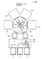
- This substrate processing apparatus 300 is divided into a unit for removing Cu-containing residue and a unit for removing a copper oxide film, and a cluster tool type multi-chamber in which these units are provided together with a unit for forming a barrier film and a Cu seed film forming unit. Configured as a system.
- the substrate processing apparatus 300 mainly forms a Cu-containing residue removal unit 101 that removes a Cu-containing residue, a copper oxide film removal unit 102 that removes a copper oxide film, and forms a barrier film on the inner walls of trenches and / or vias.
- These units 101 to 104 are held in vacuum, and are also held in vacuum.
- the chamber 105 is connected through a gate valve G.
- load lock chambers 106 and 107 are connected to the transfer chamber 105 through gate valves G.
- An air loading / unloading chamber 108 is provided on the opposite side of the load lock chambers 106 and 107 to the transfer chamber 5, and a wafer W is placed on the opposite side of the loading / unloading chamber 108 from the connecting portion of the load lock chambers 106 and 107.
- Three carrier attachment ports 109, 110, and 111 for attaching the accommodable carrier C are provided.
- the wafer W is transferred into and out of the Cu-containing residue removal unit 101, the copper oxide film removal unit 102, the barrier film formation unit 103, the Cu seed film formation unit 104, and the load lock chambers 106 and 107.
- a conveying device 112 for performing the above is provided.
- the transfer device 112 is provided at substantially the center of the transfer chamber 105, and has two support arms 114a and 114b that support the semiconductor wafer W at the tip of a rotatable / extensible / retractable portion 113 that can be rotated and extended. These two support arms 114a and 114b are attached to the rotation / extension / contraction section 113 so as to face opposite directions.
- a transfer device 116 for loading / unloading the wafer W into / from the carrier C and loading / unloading the wafer W into / from the load lock chambers 106 and 107 is provided.
- the transfer device 116 has an articulated arm structure, and can run on the rail 118 along the arrangement direction of the carrier C.
- the wafer W is placed on the support arm 117 at the tip thereof and transferred. I do.
- the substrate processing apparatus 300 includes a control unit 120 that controls each component, and thereby, each component of the units 101 to 104, the transfer devices 112 and 116, and the exhaust system (not shown) of the transfer chamber 105.
- the gate valve G is controlled to be opened and closed.
- the control unit 120 is configured similarly to the control unit 40 of FIG.
- Each of the Cu-containing residue removal unit 101 and the copper oxide removal unit 102 has the same configuration as the substrate processing apparatus of FIG.
- the temperature of the mounting table is set so that the wafer is heated to the first temperature, for example, 100 to 200 ° C.
- the copper oxide film removal unit 102 has the wafer in the second temperature.
- the temperature of the mounting table is set so as to be heated to, for example, 200 to 300 ° C.
- the Cu-containing residue 209 and the copper oxide film 210 in the structure of FIG. 2 are removed by dry cleaning with a processing gas containing an organic acid.
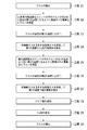
- FIG. 8 is a flowchart showing the substrate processing method of the third embodiment.
- the wafer W is loaded into one of the load lock chambers 106 and 107 from the carrier C by the transfer device 116 in the loading / unloading chamber 108 (step 21).
- the wafer W is taken out by the transfer device 112 of the transfer chamber 105, loaded into the Cu-containing material residue removal unit 101, and mounted on the mounting table therein.
- the mounting table is temperature-controlled so that the mounted wafer W has a relatively low first temperature.
- an inert gas is introduced into the chamber to stabilize the temperature of the wafer W at the first temperature (step 23), and then a processing gas containing an organic acid gas is supplied into the chamber. Then, the Cu-containing residue 209 is mainly removed by etching at the first temperature (step 24).
- the organic acid constituting the processing gas carboxylic acid can be suitably used as described above, and formic acid (HCOOH) is preferable among these.
- the first temperature is preferably in the range of 100 to 200 ° C. as in Step 4 in the first embodiment.
- a reduction reaction occurs according to the formula. This step is performed until the Cu-containing residue 209 is almost completely removed by etching. At this time, a part of the copper oxide film 210 is also removed by etching.
- processing gas may be supplied immediately after the wafer W is placed on the mounting table without performing the stabilization step of the step 23. Further, in step 24, the inert gas may be stopped even in a state where it is allowed to flow.
- the wafer W is unloaded from the Cu-containing residue removing unit 101 by the transfer device 112, loaded into the copper oxide film removing unit 102, and placed on the mounting table therein. (Step 25).
- the mounting table is temperature-controlled so that the mounted wafer W has a second temperature higher than the first temperature.
- an inert gas is introduced into the chamber to stabilize the temperature of the wafer W at the second temperature (step 26), and then a processing gas containing an organic acid gas is supplied into the chamber. Then, the copper oxide film 210 is removed mainly by reduction at the second temperature (step 27).
- the second temperature at this time is preferably in the range of 200 to 300 ° C. as in Step 6 in the first embodiment, for example, when the organic acid to be used is a carboxylic acid such as formic acid (HCOOH). 2) A reduction reaction occurs according to the formula.
- processing gas may be supplied immediately after the wafer W is mounted on the mounting table without performing the stabilization process of the process 26. Further, in step 27, the inert gas may be stopped even in a state where it is allowed to flow.
- the removal process by the reaction mainly including the reduction of the copper oxide film 210 is continued until the copper oxide film 210 is completely removed.
- the cleaning process of this embodiment is finished.
- the barrier film formation unit 103 then forms a barrier film (step 28). ) After forming the Cu seed film in the Cu seed film forming unit 104 (step 29), the Cu seed film is unloaded through either the load lock chamber 106 or 107 (step 30).
- the first temperature is relatively low.
- the Cu-containing residue is removed by etching, and the copper oxide on the surface of Cu is removed by a reaction mainly composed of reduction at a second temperature higher than the first temperature, thereby removing these in a short time and reliably. Can do.
- the first embodiment it takes time to raise the temperature of the wafer from the first temperature to the second temperature, and when processing a plurality of wafers continuously, It takes time to lower the temperature of the mounting table from the second temperature to the first temperature.
- the Cu-containing residue 209 and the copper oxide film 210 are removed using two units each having a mounting table set in advance to the first temperature and the second temperature, respectively. The time for changing the temperature becomes unnecessary, and the throughput of processing can be increased accordingly.
- a unit for performing etching of the low-k film and ashing of the resist is further mounted, and from the etching of the low-k film to the formation of the Cu seed film.
- a series of steps may be performed in-situ.
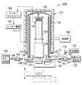
- FIG. 9 is a cross-sectional view schematically showing an example of a substrate processing apparatus used for carrying out the substrate processing method according to the fourth embodiment of the present invention.
- the substrate processing apparatus 400 is a so-called batch type apparatus that heats a plurality of wafers W at the same time, and has a substantially cylindrical processing container 131 that accommodates and processes the wafers W.
- a quartz process tube 132 having a double tube structure is provided inside the processing container 131, and a cylindrical metal manifold 136 is connected to the lower end of the process tube 132.
- Various pipes are connected to the manifold 136.
- a wafer boat 133 for holding a plurality of wafers W and holding them in the processing vessel 131 is carried in.
- the wafer boat 133 is supported by the boat elevator 134 via the heat insulating cylinder 138, and the wafer boat 133 is carried in and out by moving the wafer boat 133 up and down.
- a lid 137 is attached to the boat elevator 134. When the boat elevator 134 is raised and the wafer boat 133 is loaded into the process tube 132, the lid 137 seals the lower opening of the manifold 136 in a sealed state. The inside of the process tube 132 becomes a sealed space.
- a heater 135 for heating the wafer W is provided so as to surround the process tube 132.
- a heater power supply 141 is connected to the heater 135.
- a thermocouple 142 is provided in the vicinity of the wafer W mounted on the wafer boat 133, and a signal from the thermocouple 142 is transmitted to the heater controller 143.
- the heater controller 143 transmits a command to the heater power supply 141 in accordance with a signal from the thermocouple 142, controls the heating of the heater 135, and controls the wafer W to a predetermined temperature.
- a processing gas pipe 151 for supplying a processing gas containing an organic acid gas into the process tube 132 is connected to the manifold 136.
- the processing gas pipe 151 extends horizontally inside the manifold 136, and the tip is bent upward so that the processing gas can be supplied upward of the process tube 132.
- a processing gas supply source 152 that supplies a processing gas is connected to the other end of the processing gas pipe 151.
- the processing gas pipe 151 is provided with a mass flow controller 153 and front and rear valves 154.
- the organic acid constituting the processing gas carboxylic acid can be preferably used.
- formic acid HCOOH
- acetic acid CH 2 COOH
- propionic acid CH 2 COOH
- butyric acid CH 3 (CH 2 ) 2 COOH
- valeric acid CH 3 (CH 2 ) 3 COOH
- formic acid (HCOOH) is preferable.
- An inert gas pipe 161 for supplying an inert gas into the process tube 132 is also connected to the manifold 136.
- the inert gas pipe 161 extends horizontally inside the manifold 136 and has a tip bent upward so that the inert gas can be supplied upward of the process tube 132.
- An inert gas supply source 162 that supplies an inert gas is connected to the other end of the inert gas pipe 161.
- the inert gas pipe 161 is provided with a mass flow controller 163 and front and rear valves 164.
- the inert gas is used as a purge gas, a dilution gas, a carrier gas, and the like, and examples thereof include Ar gas, He gas, and N 2 gas.
- a pipe 171 is connected to the manifold 136 and exhausts from between the inner pipe and the outer pipe of the process tube 132.
- the exhaust pipe 171 is provided with an exhaust device 172 including a high-speed vacuum pump.
- the exhaust pipe 171 is provided with a conductance variable valve 173 so that the exhaust amount from the process tube 132 can be adjusted.
- the exhaust device 172 By operating the exhaust device 172, the gas in the process tube 132 is exhausted, and the inside of the process tube 132 can be decompressed at a high speed to a predetermined degree of vacuum via the exhaust pipe 171.
- the substrate processing apparatus 400 includes a control unit 180 that controls each component.
- the control unit 180 is configured similarly to the control unit 40 of FIG.
- the substrate processing of this embodiment is performed by removing the Cu-containing residue adhering to the copper oxide film and the interlayer insulating film on the Cu surface in the Cu wiring structure on the wafer W and cleaning it. A method will be described.
- the Cu-containing material 209 and the copper oxide film 210 in the structure of FIG. 2 are removed by dry cleaning with a processing gas containing an organic acid.
- FIG. 10 is a flowchart showing the substrate processing method of the fourth embodiment.
- a plurality of wafer boats 133 loaded with, for example, 100 wafers W are loaded into the process tube 132 by the boat elevator 134 (step 31).
- the heater 135 is controlled by the heater controller 143, and the temperature of the wafer W is relatively controlled by the etching reaction of the copper oxide that is the main component of the Cu-containing residue 209.
- the temperature is controlled to a low first temperature (step 32).
- the valve 164 is opened and, for example, Ar gas is introduced from the inert gas supply source 162 into the process tube 132 through the inert gas pipe 161. Then, the temperature of the wafer W is stabilized at the first temperature (step 33).
- the valve 154 is opened, and the processing gas containing the organic acid gas is supplied from the processing gas supply source 152 into the process tube 132 through the processing gas pipe 151 while controlling the flow rate by the mass flow controller 153.
- the material residue 209 is removed by etching (step 34). This step is performed until the Cu-containing residue 209 is almost completely removed by etching. At this time, a part of the copper oxide film 210 is also removed by etching.
- the organic acid constituting the processing gas carboxylic acid can be suitably used as described above, and formic acid (HCOOH) is preferable among these.
- the first temperature is preferably in the range of 100 to 200 ° C. as in Step 4 in the first embodiment.
- a reduction reaction occurs according to the formula.
- processing gas may be supplied immediately after the wafer W is loaded into the process tube 132 without performing the stabilization step of the step 33. Further, in step 34, the inert gas may be stopped even in a state in which it flows.
- Step 34 After the Cu-containing residue 209 is almost completely removed by the process of Step 34, the supply of the process gas is stopped, and the heater controller 143 supplies a heater based on the temperature detection signal while supplying the inert gas. 135 is controlled to control the temperature of the wafer W to a second temperature higher than the first temperature at which the reduction of copper oxide is dominant (step 35).
- the processing gas containing the organic acid gas is again supplied from the processing gas supply source 152 into the process tube 132 through the processing gas pipe 151 while controlling the flow rate by the mass flow controller 153, and the Cu wiring layer 203.
- the copper oxide film 210 is removed from the surface of the copper oxide film 210 by a reaction mainly composed of a reduction reaction (step 36).
- the second temperature at this time is preferably in the range of 200 to 300 ° C., for example, when the organic acid to be used is a carboxylic acid such as formic acid (HCOOH), and the reduction reaction occurs according to the above formula (2).
- the removal process by the reaction mainly consisting of the reduction of the copper oxide film 210 is continued until the copper oxide film 210 is completely removed.
- the valve 154 is closed to stop the supply of the processing gas, the valve 164 is opened, and the inert gas is purged from the inert gas supply source 162 as a purge gas. While being controlled, the gas is supplied into the process tube 132 through the inert gas pipe 161, and the inside of the process tube 132 is purged (step 37). Thereafter, after returning the inside of the process tube 132 to normal pressure, the boat elevator 134 is lowered and the wafer boat 133 is unloaded (step 38).
- the first temperature is relatively low.
- the Cu-containing residue is removed by etching, and the copper oxide on the surface of Cu is removed by a reaction mainly composed of reduction at a second temperature higher than the first temperature, thereby removing these in a short time and reliably. Can do.
- the temperature change time affects the processing throughput, and the throughput is lowered.
- a batch that simultaneously processes a large number of wafers for example, 100 wafers. Since the processing is employed, even if it takes time for the temperature to change from the first temperature to the second temperature, the additional time per sheet is very short, and the processing throughput is hardly reduced.
- the present invention can be variously modified without being limited to the above embodiment.
- a carboxylic acid typified by formic acid (HCOOH) is used alone as the organic acid gas constituting the processing gas.
- the organic acid gas may be mixed with other gas such as hydrogen (H 2 ) and supplied.
- the apparatus for carrying out the substrate processing method of the present invention is not limited to the one shown in the above embodiment, and various apparatuses can be employed.
- the structure of the substrate to be processed is not limited to that shown in FIG. 2, and the substrate to be processed is not limited to a semiconductor wafer.
Landscapes
- Internal Circuitry In Semiconductor Integrated Circuit Devices (AREA)
- Drying Of Semiconductors (AREA)
- Cleaning Or Drying Semiconductors (AREA)
Abstract
Description
を含む基板処理方法が提供される。
(第1の実施形態の基板処理方法を実施するための基板処理装置の構成)
図1は、本発明の第1の実施形態に係る基板処理方法を実施するために用いられる基板処理装置の一例を模式的に示す断面図である。ここでは、基板として半導体ウエハ(以下、単にウエハと記す)を用いた場合について説明する(以下の実施形態も同じ)。
次に、このような基板処理装置100を用いて、ウエハW上のCu配線構造におけるCu表面の酸化銅膜と層間絶縁膜に付着したCu含有物残渣を除去してクリーニングする本実施形態の基板処理方法について説明する。
ここでCu(HCOO)は揮発性を有するため、Cu含有残渣物209はエッチング除去される。
(第2の実施形態の成膜方法を実施するための成膜装置の構成)
図5は、本発明の第2の実施形態に係る基板処理方法を実施するために用いられる基板処理装置の一例を模式的に示す断面図である。
次に、このような処理装置200を用いて、ウエハW上のCu配線構造におけるCu表面の酸化銅膜と層間絶縁膜に付着したCu含有物残渣を除去してクリーニングする本実施形態の基板処理方法について説明する。
(第3の実施形態の成膜方法を実施するための成膜装置の構成)
図7は、本発明の第3の実施形態に係る基板処理方法を実施するために用いられる基板処理装置の一例を模式的に示す断面図である。
次に、以上のように構成された基板処理装置300を用いて、ウエハW上のCu配線構造におけるCu表面の酸化銅膜と層間絶縁膜に付着したCu含有物残渣を除去してクリーニングする本実施形態の基板処理方法について説明する。
(第4の実施形態の成膜方法を実施するための成膜装置の構成)
図9は、本発明の第4の実施形態に係る基板処理方法を実施するために用いられる基板処理装置の一例を模式的に示す断面図である。
次に、このような処理装置400を用いて、ウエハW上のCu配線構造におけるCu表面の酸化銅膜と層間絶縁膜に付着したCu含有物残渣を除去してクリーニングする本実施形態の基板処理方法について説明する。
なお、本発明は、上記実施の形態に限定されることなく種々変形可能である。例えば、上記実施形態においては、処理ガスを構成する有機酸ガスとして蟻酸(HCOOH)に代表されるカルボン酸を単体で用いた例について示したが、 有機酸ガス単体で供給する場合に限らず、有機酸ガスを水素(H2)等の他のガスと混合して供給してもよい。さらに、本発明の基板処理方法を実施する装置としては、上記実施形態に示したものに限らず、種々の装置を採用することができる。さらにまた、被処理基板の構造も図2のものに限るものではなく、被処理基板も半導体ウエハに限るものではない。
Claims (14)
- 基板上のCu配線構造におけるCu表面の酸化銅膜および層間絶縁膜に付着したCu含有物残渣を有機酸含有ガスを用いて除去する基板処理方法であって、
基板温度が相対的に低温の第1の温度になるように基板を加熱しつつ基板に有機酸ガスを含む処理ガスを供給してCu含有物残渣のエッチング除去を行う工程と、
基板温度が前記第1の温度よりも高温の第2の温度になるように基板を加熱しつつ基板に有機酸ガスを含む処理ガスを供給して前記Cu表面の酸化銅膜を還元を主体とする反応により除去する工程と
を含む基板処理方法。 - 前記層間絶縁膜がLow-k膜である請求項1に記載の基板処理方法
- 前記有機酸は、カルボン酸である請求項1に記載の基板処理方法。
- 前記カルボン酸は、蟻酸である請求項3に記載の基板処理方法。
- 前記第1の温度は100~200℃であり、前記第2の温度は200~300℃である請求項3に記載の基板処理方法。
- 基板を収容するチャンバと、前記チャンバ内で基板を載置する載置台と、前記載置台上の基板を加熱する加熱機構と、前記チャンバ内に有機酸ガスを含む処理ガスを供給する処理ガス供給機構と、前記チャンバ内を排気する排気機構とを有する基板処理装置を用い、
基板を前記載置台に載置し、前記加熱機構により基板を前記第1の温度に加熱して前記Cu含有物残渣のエッチング除去を行い、次いで、前記加熱機構により基板の温度を前記第2の温度に上昇させた後、前記Cu表面の酸化銅膜の除去を行う請求項1に記載の基板処理方法。 - 基板を収容するチャンバと、前記チャンバ内で基板を載置する載置台と、前記載置台上の基板を加熱する加熱機構と、前記載置台上の基板に加熱されたエネルギー媒体ガスを供給するエネルギー媒体ガス供給機構と、前記チャンバ内に有機酸ガスを含む処理ガスを供給する処理ガス供給機構と、前記チャンバ内を排気する排気機構とを有する基板処理装置を用い、
基板を前記載置台に載置し、前記加熱機構により基板を前記第1の温度に加熱して前記Cu含有物残渣のエッチング除去を行い、次いで、前記載置台上の基板に前記エネルギー媒体ガス供給機構から加熱されたエネルギー媒体ガスを供給して基板の温度を前記第2の温度に上昇させた後、前記Cu表面の酸化銅膜の除去を行う請求項1に記載の基板処理方法。 - 載置された基板を前記第1の温度に加熱可能な温度に保持された載置台を有し、前記載置台上の基板に前記処理ガスを供給可能な第1の処理部と、載置された基板を前記第2の温度に加熱可能な温度に保持された載置台を有し、前記載置台上の基板に処理ガスを供給可能な第2の処理部とを有する基板処理装置を用い、
前記第1の処理部の載置台に基板を載置し、基板を前記第1の温度に加熱して前記前記Cu含有物残渣のエッチング除去を行い、次いで前記第2の処理部の載置台に基板を載置し、基板を前記第2の温度に加熱して前記Cu表面の酸化銅膜の除去を行う請求項1に記載の基板処理方法。 - 基板を処理する処理容器と、前記処理容器内で複数の基板を保持する基板保持部と、前記処理容器内の複数の基板を加熱する加熱機構と、前記処理容器内に有機酸ガスを含む処理ガスを供給する処理ガス供給機構と、前記処理容器内を排気する排気機構とを有する基板処理装置を用い、
前記保持手段に保持された基板を前記処理容器内に収容し、前記加熱機構により複数の基板を前記第1の温度に加熱して前記Cu含有物残渣のエッチング除去を行い、次いで、前記加熱機構により複数の基板の温度を前記第2の温度に上昇させた後、前記Cu表面の酸化銅膜の除去を行う請求項1に記載の基板処理方法。 - 基板上のCu配線構造におけるCu表面の酸化銅膜および層間絶縁膜に付着したCu含有物残渣を有機酸含有ガスを用いて除去する基板処理装置であって、
基板を収容するチャンバと、
前記チャンバ内で基板を載置する載置台と、
前記載置台上の基板を加熱する加熱機構と、
前記チャンバ内に有機酸ガスを含む処理ガスを供給する処理ガス供給機構と、
前記チャンバ内を排気する排気機構と、
前記載置台に基板が載置された状態で、前記加熱機構により基板を相対的に低温の第1の温度に加熱しつつ基板に有機酸ガスを含む処理ガスを供給してCu含有物残渣のエッチング除去を行わせ、次いで、前記加熱機構により基板の温度を前記第1の温度よりも高温の第2の温度に上昇させた後、基板に有機酸ガスを含む処理ガスを供給して前記Cu表面の酸化銅膜を還元を主体とする反応により除去させるように制御する制御機構と
を具備する基板処理装置。 - 基板上のCu配線構造におけるCu表面の酸化銅膜および層間絶縁膜に付着したCu含有物残渣を有機酸含有ガスを用いて除去する基板処理装置であって、
基板を収容するチャンバと、
前記チャンバ内で基板を載置する載置台と、
前記載置台上の基板を加熱する加熱機構と、
前記載置台上の基板に加熱されたエネルギー媒体ガスを供給するエネルギー媒体ガス供給機構と、
前記チャンバ内に有機酸ガスを含む処理ガスを供給する処理ガスと、
前記チャンバ内を排気する排気機構と、
前記載置台に基板が載置された状態で、前記加熱機構により基板を相対的に低温の第1の温度に加熱しつつ基板に有機酸ガスを含む処理ガスを供給してCu含有物残渣のエッチング除去を行わせ、次いで、前記載置台上の基板に加熱されたエネルギー媒体ガスを供給して基板の温度を前記第1の温度よりも高温の第2の温度に上昇させた後、基板に有機酸ガスを含む処理ガスを供給して前記Cu表面の酸化銅膜を還元を主体とする反応により除去させるように制御する制御機構と
を具備する基板処理装置。 - 基板上のCu配線構造におけるCu表面の酸化銅膜および層間絶縁膜に付着したCu含有物残渣を有機酸含有ガスを用いて除去する基板処理装置であって、
載置された基板を前記第1の温度に加熱可能な温度に保持された載置台を有し、前記載置台上の基板に前記処理ガスを供給可能な第1の処理部と、
載置された基板を前記第2の温度に加熱可能な温度に保持された載置台を有し、前記載置台上の基板に処理ガスを供給可能な第2の処理部と、
前記第1の処理部と前記第2の処理部との間で基板を搬送する搬送機構と、
前記第1の処理部の載置台に基板を載置させ、基板を前記の第1の温度に加熱しつつ基板に有機酸ガスを含む処理ガスを供給してCu含有物残渣のエッチング除去を行わせ、次いで、前記搬送機構により基板を前記第2の処理部の載置台に搬送させ、基板を前記第2の温度に加熱しつつ基板に有機酸ガスを含む処理ガスを供給して前記Cu表面の酸化銅膜を還元を主体とする反応により除去させるように制御する制御機構と
を具備する基板処理装置。 - 基板上のCu配線構造におけるCu表面の酸化銅膜および層間絶縁膜に付着したCu含有物残渣を有機酸含有ガスを用いて除去する基板処理装置であって、
基板を処理する処理容器と、
前記処理容器内で複数の基板を保持する基板保持部と、
前記処理容器内の複数の基板を加熱する加熱機構と、
前記処理容器内に有機酸ガスを含む処理ガスを供給する処理ガス供給機構と、
複数の基板が保持された状態の前記基板保持部を前記処理容器内に収容させた状態で、前記加熱機構により複数の基板を相対的に低温の第1の温度に加熱しつつ複数の基板に有機酸ガスを含む処理ガスを供給してCu含有物残渣のエッチング除去を行わせ、次いで、前記加熱機構により複数の基板の温度を前記第1の温度よりも高温の第2の温度に上昇させた後、複数の基板に有機酸ガスを含む処理ガスを供給して前記Cu表面の酸化銅膜を還元を主体とする反応により除去させるように制御する制御機構と
を具備する基板処理装置。 - コンピュータ上で動作し、基板処理装置を制御するためのプログラムが記憶された記憶媒体であって、
前記プログラムは、実行時に、
基板上のCu配線構造におけるCu表面の酸化銅膜および層間絶縁膜に付着したCu含有物残渣を有機酸含有ガスを用いて除去する基板処理方法であって、
基板温度が相対的に低温の第1の温度になるように基板を加熱しつつ基板に有機酸ガスを含む処理ガスを供給してCu含有物残渣のエッチング除去を行う工程と、
基板温度が前記第1の温度よりも高温の第2の温度になるように基板を加熱しつつ基板に有機酸ガスを含む処理ガスを供給して前記Cu表面の酸化銅膜を還元を主体とする反応により除去する工程と
を含む基板処理方法が行われるように、コンピュータに前記基板処理装置を制御させる記憶媒体。
Priority Applications (3)
| Application Number | Priority Date | Filing Date | Title |
|---|---|---|---|
| KR1020117023900A KR101296960B1 (ko) | 2009-03-19 | 2010-02-04 | 기판 처리 방법 및 기판 처리 장치 |
| CN2010800128077A CN102356453A (zh) | 2009-03-19 | 2010-02-04 | 基板处理方法和基板处理装置 |
| US13/235,955 US20120006782A1 (en) | 2009-03-19 | 2011-09-19 | Substrate processing method and substrate processing apparatus |
Applications Claiming Priority (2)
| Application Number | Priority Date | Filing Date | Title |
|---|---|---|---|
| JP2009067919A JP5161819B2 (ja) | 2009-03-19 | 2009-03-19 | 基板処理方法および基板処理装置 |
| JP2009-067919 | 2009-03-19 |
Related Child Applications (1)
| Application Number | Title | Priority Date | Filing Date |
|---|---|---|---|
| US13/235,955 Continuation US20120006782A1 (en) | 2009-03-19 | 2011-09-19 | Substrate processing method and substrate processing apparatus |
Publications (1)
| Publication Number | Publication Date |
|---|---|
| WO2010106843A1 true WO2010106843A1 (ja) | 2010-09-23 |
Family
ID=42739509
Family Applications (1)
| Application Number | Title | Priority Date | Filing Date |
|---|---|---|---|
| PCT/JP2010/051597 Ceased WO2010106843A1 (ja) | 2009-03-19 | 2010-02-04 | 基板処理方法および基板処理装置 |
Country Status (5)
| Country | Link |
|---|---|
| US (1) | US20120006782A1 (ja) |
| JP (1) | JP5161819B2 (ja) |
| KR (1) | KR101296960B1 (ja) |
| CN (1) | CN102356453A (ja) |
| WO (1) | WO2010106843A1 (ja) |
Families Citing this family (9)
| Publication number | Priority date | Publication date | Assignee | Title |
|---|---|---|---|---|
| JP5395708B2 (ja) * | 2010-03-09 | 2014-01-22 | 東京エレクトロン株式会社 | 基板の配線方法及び半導体製造装置 |
| WO2014132961A1 (ja) * | 2013-03-01 | 2014-09-04 | 戸田工業株式会社 | 導電性塗膜の製造方法及び導電性塗膜 |
| JP5800969B1 (ja) * | 2014-08-27 | 2015-10-28 | 株式会社日立国際電気 | 基板処理装置、半導体装置の製造方法、プログラム、記録媒体 |
| EP3061845B1 (en) * | 2015-02-03 | 2018-12-12 | LG Electronics Inc. | Metal organic chemical vapor deposition apparatus for solar cell |
| CN111607801A (zh) * | 2019-02-22 | 2020-09-01 | 中科院微电子研究所昆山分所 | 一种铜表面氧化物的处理方法 |
| JP7341043B2 (ja) * | 2019-12-06 | 2023-09-08 | 東京エレクトロン株式会社 | 基板処理方法及び基板処理装置 |
| CN111088501B (zh) * | 2019-12-16 | 2021-06-22 | 浙江大学 | 一种元素分析仪还原管的回收和再利用方法 |
| JP7030858B2 (ja) * | 2020-01-06 | 2022-03-07 | 株式会社Kokusai Electric | 半導体装置の製造方法、基板処理装置およびプログラム |
| JP7828857B2 (ja) * | 2022-08-30 | 2026-03-12 | 株式会社アルバック | 基板処理装置、基板処理システム、および基板処理方法 |
Citations (3)
| Publication number | Priority date | Publication date | Assignee | Title |
|---|---|---|---|---|
| JP2006216937A (ja) * | 2005-01-06 | 2006-08-17 | Ebara Corp | 基板処理方法及び装置 |
| WO2008001697A1 (fr) * | 2006-06-26 | 2008-01-03 | Tokyo Electron Limited | Procédé et appareil de traitement de substrats |
| JP2009043975A (ja) * | 2007-08-09 | 2009-02-26 | Tokyo Electron Ltd | ドライクリーニング方法、基板処理装置、半導体装置の製造方法及び記憶媒体 |
Family Cites Families (8)
| Publication number | Priority date | Publication date | Assignee | Title |
|---|---|---|---|---|
| JPS57170534A (en) * | 1981-04-15 | 1982-10-20 | Hitachi Ltd | Dry etching method for aluminum and aluminum alloy |
| JPS63203772A (ja) * | 1987-02-20 | 1988-08-23 | Hitachi Ltd | 銅薄膜の気相成長方法 |
| US6899816B2 (en) * | 2002-04-03 | 2005-05-31 | Applied Materials, Inc. | Electroless deposition method |
| US7205228B2 (en) * | 2003-06-03 | 2007-04-17 | Applied Materials, Inc. | Selective metal encapsulation schemes |
| JP4590402B2 (ja) * | 2004-04-30 | 2010-12-01 | 株式会社荏原製作所 | 基板の処理装置 |
| WO2006073140A1 (en) * | 2005-01-06 | 2006-07-13 | Ebara Corporation | Substrate processing method and apparatus |
| US20070054047A1 (en) * | 2005-09-06 | 2007-03-08 | Tokyo Electron Limited | Method of forming a tantalum-containing layer from a metalorganic precursor |
| JP2009043974A (ja) * | 2007-08-09 | 2009-02-26 | Tokyo Electron Ltd | 半導体装置の製造方法、半導体基板の処理装置及び記憶媒体 |
-
2009
- 2009-03-19 JP JP2009067919A patent/JP5161819B2/ja not_active Expired - Fee Related
-
2010
- 2010-02-04 WO PCT/JP2010/051597 patent/WO2010106843A1/ja not_active Ceased
- 2010-02-04 CN CN2010800128077A patent/CN102356453A/zh active Pending
- 2010-02-04 KR KR1020117023900A patent/KR101296960B1/ko not_active Expired - Fee Related
-
2011
- 2011-09-19 US US13/235,955 patent/US20120006782A1/en not_active Abandoned
Patent Citations (3)
| Publication number | Priority date | Publication date | Assignee | Title |
|---|---|---|---|---|
| JP2006216937A (ja) * | 2005-01-06 | 2006-08-17 | Ebara Corp | 基板処理方法及び装置 |
| WO2008001697A1 (fr) * | 2006-06-26 | 2008-01-03 | Tokyo Electron Limited | Procédé et appareil de traitement de substrats |
| JP2009043975A (ja) * | 2007-08-09 | 2009-02-26 | Tokyo Electron Ltd | ドライクリーニング方法、基板処理装置、半導体装置の製造方法及び記憶媒体 |
Also Published As
| Publication number | Publication date |
|---|---|
| US20120006782A1 (en) | 2012-01-12 |
| JP2010225614A (ja) | 2010-10-07 |
| JP5161819B2 (ja) | 2013-03-13 |
| KR101296960B1 (ko) | 2013-08-14 |
| CN102356453A (zh) | 2012-02-15 |
| KR20110127268A (ko) | 2011-11-24 |
Similar Documents
| Publication | Publication Date | Title |
|---|---|---|
| JP5161819B2 (ja) | 基板処理方法および基板処理装置 | |
| JP5497278B2 (ja) | 銅の異方性ドライエッチング方法および装置 | |
| TWI806835B (zh) | 蝕刻方法及dram電容器之製造方法 | |
| JP5452894B2 (ja) | 基板処理方法、基板処理装置および記憶媒体 | |
| JP5193913B2 (ja) | CVD−Ru膜の形成方法および半導体装置の製造方法 | |
| JP4294696B2 (ja) | 半導体装置の製造方法および製造装置、ならびに記憶媒体 | |
| JP6139986B2 (ja) | エッチング方法 | |
| JP5261291B2 (ja) | 処理方法および記憶媒体 | |
| JPWO2013175872A1 (ja) | ガス処理方法 | |
| CN101496147B (zh) | 热处理方法 | |
| JP4675127B2 (ja) | 薄膜形成装置、薄膜形成装置の洗浄方法及びプログラム | |
| JP2008198848A (ja) | 処理方法および記憶媒体 | |
| JP5997555B2 (ja) | エッチング装置およびエッチング方法 | |
| JP6559046B2 (ja) | パターン形成方法 | |
| JP2015073035A (ja) | エッチング方法 | |
| JP2012174843A (ja) | 金属薄膜の成膜方法、半導体装置及びその製造方法 | |
| WO2010103879A1 (ja) | Cu膜の成膜方法および記憶媒体 | |
| CN102723305B (zh) | 膜的处理方法 | |
| JP5188212B2 (ja) | ドライクリーニング方法、基板処理装置および記憶媒体 | |
| JP5938164B2 (ja) | 成膜方法、成膜装置、半導体装置及びその製造方法 | |
| JP2010027787A (ja) | 終点検出方法、基板処理方法、基板処理装置および基板処理システム | |
| JP5535368B2 (ja) | 処理装置 | |
| JP5661444B2 (ja) | 薄膜形成装置、薄膜形成装置の洗浄方法及びプログラム | |
| WO2019058554A1 (ja) | 半導体装置の製造方法、基板処理装置およびプログラム | |
| WO2009087906A1 (ja) | 成膜方法および成膜装置 |
Legal Events
| Date | Code | Title | Description |
|---|---|---|---|
| WWE | Wipo information: entry into national phase |
Ref document number: 201080012807.7 Country of ref document: CN |
|
| 121 | Ep: the epo has been informed by wipo that ep was designated in this application |
Ref document number: 10753338 Country of ref document: EP Kind code of ref document: A1 |
|
| NENP | Non-entry into the national phase |
Ref country code: DE |
|
| ENP | Entry into the national phase |
Ref document number: 20117023900 Country of ref document: KR Kind code of ref document: A |
|
| 122 | Ep: pct application non-entry in european phase |
Ref document number: 10753338 Country of ref document: EP Kind code of ref document: A1 |