WO2010103962A1 - 光学的情報再生方法、光ヘッドおよび光ディスク装置 - Google Patents
光学的情報再生方法、光ヘッドおよび光ディスク装置 Download PDFInfo
- Publication number
- WO2010103962A1 WO2010103962A1 PCT/JP2010/053387 JP2010053387W WO2010103962A1 WO 2010103962 A1 WO2010103962 A1 WO 2010103962A1 JP 2010053387 W JP2010053387 W JP 2010053387W WO 2010103962 A1 WO2010103962 A1 WO 2010103962A1
- Authority
- WO
- WIPO (PCT)
- Prior art keywords
- optical
- light
- path length
- optical path
- length difference
- Prior art date
- Legal status (The legal status is an assumption and is not a legal conclusion. Google has not performed a legal analysis and makes no representation as to the accuracy of the status listed.)
- Ceased
Links
Images


Classifications
-
- G—PHYSICS
- G11—INFORMATION STORAGE
- G11B—INFORMATION STORAGE BASED ON RELATIVE MOVEMENT BETWEEN RECORD CARRIER AND TRANSDUCER
- G11B7/00—Recording or reproducing by optical means, e.g. recording using a thermal beam of optical radiation by modifying optical properties or the physical structure, reproducing using an optical beam at lower power by sensing optical properties; Record carriers therefor
- G11B7/004—Recording, reproducing or erasing methods; Read, write or erase circuits therefor
- G11B7/005—Reproducing
-
- G—PHYSICS
- G11—INFORMATION STORAGE
- G11B—INFORMATION STORAGE BASED ON RELATIVE MOVEMENT BETWEEN RECORD CARRIER AND TRANSDUCER
- G11B7/00—Recording or reproducing by optical means, e.g. recording using a thermal beam of optical radiation by modifying optical properties or the physical structure, reproducing using an optical beam at lower power by sensing optical properties; Record carriers therefor
- G11B7/08—Disposition or mounting of heads or light sources relatively to record carriers
- G11B7/09—Disposition or mounting of heads or light sources relatively to record carriers with provision for moving the light beam or focus plane for the purpose of maintaining alignment of the light beam relative to the record carrier during transducing operation, e.g. to compensate for surface irregularities of the latter or for track following
- G11B7/0941—Methods and circuits for servo gain or phase compensation during operation
-
- G—PHYSICS
- G11—INFORMATION STORAGE
- G11B—INFORMATION STORAGE BASED ON RELATIVE MOVEMENT BETWEEN RECORD CARRIER AND TRANSDUCER
- G11B7/00—Recording or reproducing by optical means, e.g. recording using a thermal beam of optical radiation by modifying optical properties or the physical structure, reproducing using an optical beam at lower power by sensing optical properties; Record carriers therefor
- G11B7/12—Heads, e.g. forming of the optical beam spot or modulation of the optical beam
- G11B7/135—Means for guiding the beam from the source to the record carrier or from the record carrier to the detector
- G11B7/1359—Single prisms
-
- G—PHYSICS
- G11—INFORMATION STORAGE
- G11B—INFORMATION STORAGE BASED ON RELATIVE MOVEMENT BETWEEN RECORD CARRIER AND TRANSDUCER
- G11B7/00—Recording or reproducing by optical means, e.g. recording using a thermal beam of optical radiation by modifying optical properties or the physical structure, reproducing using an optical beam at lower power by sensing optical properties; Record carriers therefor
- G11B2007/0003—Recording, reproducing or erasing systems characterised by the structure or type of the carrier
- G11B2007/0009—Recording, reproducing or erasing systems characterised by the structure or type of the carrier for carriers having data stored in three dimensions, e.g. volume storage
- G11B2007/0013—Recording, reproducing or erasing systems characterised by the structure or type of the carrier for carriers having data stored in three dimensions, e.g. volume storage for carriers having multiple discrete layers
Definitions
- the present invention relates to a high S / N ratio of a reproduction signal of an optical disc apparatus.
- Optical discs have reached the limit of the resolution of the optical system, resulting in the commercialization of a blue-ray disc using a blue semiconductor laser and a high NA objective lens.
- the recording layer will be multilayered in the future. It is thought to be influential.
- the reflectance from a specific recording layer must be reduced because the amount of light detected from each recording layer needs to be substantially equal.
- the optical disk needs to have a large capacity and a high dubbing speed for video and the like, the data transfer speed is also increasing, and the S / N ratio of the reproduced signal cannot be secured sufficiently. Therefore, in order to simultaneously advance the multilayering and speeding up of the recording layer in the future, it is essential to increase the S / N of the detection signal.
- Patent Document 1 and Patent Document 2 relate to increasing the S / N ratio of a reproduction signal of a magneto-optical disk, and branch light before irradiating the optical disk with light from a semiconductor laser, and reflect light that does not irradiate the optical disk from reflected light from the optical disk. Is intended to amplify the amplitude of a weak signal by increasing the amount of light that does not irradiate the optical disk.
- the original incident polarization component and the incident polarization direction caused by the polarization rotation by the magneto-optical disk Detection is performed by interfering orthogonal polarization components and amplifying the orthogonal polarization components with incident polarization. Therefore, if the original incident polarization component is increased, the signal can be increased, but the intensity of the light incident on the optical disk must be kept below a certain level in order not to erase or overwrite the data. There is.
- the light to be interfered with the signal light is separated in advance, and this is interfered with the signal light without condensing it on the disk, and the intensity of the light to be interfered for signal amplification is This makes it possible to increase the intensity regardless of the light intensity on the disk surface.
- the S / N ratio compared to the noise of the amplifier that converts the photocurrent from the photodetector into a voltage can be increased as the intensity is increased within the range allowed by the light intensity.
- Patent Document 3 relates to a high S / N ratio of a reproduction signal of an optical disk using a photochromic medium, and in the same manner as in Reference Documents 1 and 2, a signal is generated by interfering light that does not irradiate an optical disk with reflected light from the optical disk. Aiming for amplification. Also for an optical disk using a photochromic medium, the higher the incident light intensity for signal reproduction, the faster the medium is deteriorated. Therefore, similarly to the magneto-optical disk, the intensity of light applied to the recording medium is limited.
- Patent Document 1 interference light intensity is detected by causing two lights to interfere with each other. At this time, the optical path length of the reflected disk light to be interfered is made variable so as to secure the interference signal amplitude.
- Patent Document 2 Patent Document 3, and Patent Document 4, differential detection is performed in addition to interference light intensity detection. As a result, the intensity component of each light that does not contribute to the signal is canceled and the signal amplitude is doubled to achieve a high S / N ratio.
- an interference signal obtained by interference between two lights depends on a phase difference (optical path length difference) between the two lights to be interfered.
- Patent Document 1 stabilizes the optical path length difference by making a triangular prism inserted in the optical path movable in the direction of the incident optical axis.
- Patent Document 4 the entire optical interference system is caused to follow the optical disc, thereby canceling the optical path length difference caused by the surface blur caused by the rotation of the optical disc.
- the optical path length difference is stabilized by making the position of the mirror that reflects the light not hitting the optical disc movable in the optical axis direction.
- Patent Document 5 a plurality of interference signals having different interference states are generated from the optical path length difference, and an amplified signal that does not depend on the phase difference is output by generating a signal by calculating these interference signals.
- the object to be moved is made to follow about 600 ⁇ m of the current optical disc surface deviation, and the phase difference between the signal light and the reference light is fixed, that is, the light source It is necessary to perform positioning with an accuracy of about several nanometers sufficiently smaller than the wavelength.
- unevenness in the thickness of the cover layer provided on the optical disk also causes the optical path length difference to be disturbed.
- a method for controlling the optical path length corresponding to the uneven thickness is not particularly described.
- Patent Document 5 employs a method of obtaining an output that does not depend on the optical path length difference, so the above problem does not occur.
- a signal processing process for obtaining an output that does not depend on the optical path length difference non-linear computation or the like is performed. Since complicated arithmetic processing is required, the burden on the signal processing circuit increases. Also, since the output does not depend on the optical path length difference from multiple interference signals, thermal noise mixed into each interference signal is added and noise increases, or noise is mixed due to imperfect computation processing Therefore, the above arithmetic processing becomes a factor that degrades the signal quality. Furthermore, in order to obtain an output that does not depend on the optical path length difference, high accuracy is required for various parameters of the optical system, and the construction of the optical system becomes very difficult.
- a first object of the present invention is to provide an interference-type optical information signal reproduction method that can easily adjust the optical path difference between two lights, has a high signal amplification effect, and is suitable for downsizing an optical system. Is to provide.
- a second object of the present invention is to provide an optical head equipped with an interference type optical information signal detection system that can easily adjust an optical path difference between two lights, has a high signal amplification effect, and is suitable for downsizing of an optical system. Is to provide.
- a third object of the present invention is to provide an optical disc apparatus equipped with an interference type optical information signal detection system that can easily adjust an optical path difference between two lights, has a high signal amplification effect, and is suitable for downsizing of an optical system. Is to provide.
- the above-described problem is solved by performing the length adjustment in three parts: coarse adjustment of the optical path length difference, fine adjustment, and optical path length difference fixed position adjustment.
- the rough adjustment of the optical path length difference is an adjustment for canceling the optical path difference between the signal light and the reference light, which is generated based on fluctuations in the relative distance between the optical head and the optical information recording medium (for example, optical disc surface shake).
- the definition of the fine adjustment of the optical path difference and the adjustment of the optical path length difference fixed position will be described later.
- An interference type optical disc device, an optical head, and a signal reproducing method that can be manufactured in the same size as a conventional disc device, have a high signal amplification effect, and are inexpensive are realized.
- the basic embodiment of the present invention The figure showing the detail of the detector for servo detection.
- the figure which shows an optical head in case the detector which detects an interference signal is three.
- the figure which shows an optical head in case a reference light reflection means and an interference light detection optical system differ.
- the figure which shows the structure of the interference optical system and detector of the optical head of FIG. The figure which shows the structure of the detector of the optical head of FIG.
- the figure which shows an optical head in case a corner cube prism and an objective lens are mounted in a separate actuator.
- Explanatory drawing of the optical path length difference fine adjustment by a phase jump Explanatory drawing of the method of performing an optical path length fine adjustment with the combination of an optical path length zero position adjustment mechanism and an optical path length difference fine adjustment mechanism.
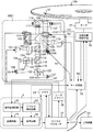
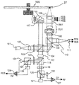
- FIG. 1 shows an example of the overall configuration of the optical disk apparatus of the present embodiment.
- the optical disk apparatus shown in FIG. 1 roughly includes disk support means including a spindle motor 77 that holds the optical disk 109, an optical head (optical pickup) 2001 that inputs / outputs various data to / from the optical disk 109, and operations of the entire optical disk apparatus.
- the microprocessor 27 on which the firmware to be controlled operates, the reproduction signal processing block 2 that performs various processes on the reproduction signal of the optical head, the memory 29 that stores various control parameters and control tables, and the optical head 2001 are mounted.
- Each optical element constituting the optical head system described below is integrally formed as an optical module.
- the optical head optical system of the present embodiment is generated by an interference optical system for guiding the light emitted from the laser light to the optical disc and reflecting it, and causing the reflected light and the reference signal to interfere to generate interference light.
- the detection optical system is configured to separate the interference light, add a phase difference to each of the separated interference lights, and detect with a plurality of detectors.
- the polarization beam splitter 104 transmits almost 100% of p-polarized light (hereinafter referred to as horizontal polarization) incident on the separation surface and reflects almost 100% of s-polarized light (hereinafter referred to as vertical polarization), that is, transmitted light and reflected light. It has a function of separating light. At this time, the intensity ratio of the transmitted light and the reflected light can be adjusted by adjusting the rotation angle of the ⁇ / 2 plate 103 around the optical axis.
- the transmitted light is incident on the special polarization beam splitter 105.
- the special polarizing beam splitter 105 has a property of transmitting 100% of horizontally polarized light, reflecting part of vertically polarized light, and partially transmitting. Therefore, the incident light is 100% transmitted, is transmitted through the ⁇ / 4 plate 106 and converted into circularly polarized light, passes through the beam expander 1101 that corrects spherical aberration, and is mounted on the two-dimensional actuator 107. Thus, the light is condensed on the recording layer on the optical disk 109.
- Reflected light from the optical disk returns to the same optical path, is converted into parallel light by the objective lens 108, and is 90 ° polarization direction from the time of first incident by passing through the ⁇ / 4 plate 106 again. Becomes the linearly polarized light rotated.
- the light is incident on the special polarization beam splitter 105, and a part of the light is transmitted and a part of the light is reflected by the above properties.
- the reflected light is incident on the detector 111 by the cylindrical lens 110.
- the detector 111 is divided into four detectors 201, 202, 203, and 204 as shown in FIG. 2.
- the detector 111 shown in FIG. 2 includes a logical operation circuit for executing the operation AB ⁇ C + D and the operation AB + CD.
- the light transmitted through the special polarization beam splitter 105 enters the polarization beam splitter 104. Then, since the polarized light is rotated 90 degrees, it is reflected and enters the condenser lens 113 (hereinafter, this reflected light is referred to as reference light).
- this reflected light is referred to as reference light.
- the light emitted from the semiconductor laser 101 and reflected by the polarization beam splitter 104 is reflected by the reflecting prism 115 mounted on the movable portion 114 and enters the corner cube prism 116 mounted on the two-dimensional actuator 107.
- the corner cube prism 116 is an element that reflects incident light in the opposite direction.
- the incident light is incident on the vertex formed by the three reflecting surfaces of the corner cube prism 116.
- the light reflected thereby returns along the same optical path and enters the polarization beam splitter 104.
- the disturbance is compensated by the polarization compensator 117 inserted in the middle of the optical path, and the return light is polarized with respect to the forward light. It is rotated 90 degrees.
- the reflected light from the corner cube prism 116 passes through the polarization beam splitter 104 and enters the condensing lens 113 coaxially with the reflected light from the optical disc being orthogonal to each other.
- interference light between the reference light and the signal light is formed by the polarization beam splitter 104.
- the signal light and the reference light are orthogonal, and the interference light is called in the sense that the net polarization state differs depending on the phase relationship between the signal light and the reference light.
- Interference (appearing as a change in intensity) occurs only after being separated by the polarization beam splitters 120 and 124 in the interference optical system described below.
- the two lights incident on the condenser lens are reflected and transmitted by the non-polarizing beam splitter 118 at a ratio of 1: 1, respectively.
- the transmitted light is transmitted through the ⁇ / 2 plate 119 and the polarization is rotated by 45 degrees, and then separated by the polarization beam splitter 120 into a horizontal polarization component and a vertical polarization component, and the separated lights are detected by the detectors 121 and 122. Detected by.
- the light reflected by the non-polarizing beam splitter 118 passes through a ⁇ / 4 plate 123 whose optical axis direction is set to 45 degrees with respect to the horizontal direction, and then is separated into a horizontal polarization component and a vertical polarization component by the polarization beam splitter 124.
- the separated lights are detected by detectors 125 and 126.
- the output signals of the detectors 121 and 122 are input to the differential circuit 127, and the differential signal D1 is output. This becomes a reproduction signal (RF).
- the output signals of the detectors 125 and 126 are input to the differential circuit 128, and the differential signal D2 is output.
- the detectors 125 and 126 have a sufficiently narrower band than the reproduction signal, and the differential signal is output in a state where the reproduction signal component is removed.
- phase error signal PES
- the piezo element 129 expands and contracts according to the driving voltage, moves the mirror 130 attached on the optical path for signal light of the interference optical system back and forth, and adjusts the optical path length of the signal light to adjust the signal light and the reference light. It has a function of adjusting the phase difference (hereinafter referred to as interference phase) (interference phase adjustment is hereinafter referred to as optical path length difference fine adjustment). That is, in the present embodiment, the piezo element 129 and the mirror 130 constitute an optical path length difference fine adjustment unit.
- the optical path length difference between the signal light and the reference light needs to be set within about the coherence length of the light source.
- the movable unit 114 moves the reflecting prism 115 in the optical axis direction of the incident light according to the layer to be read of the multilayer optical disk, the type of the disk, etc. Adjustment is performed so that the difference is sufficiently smaller than the coherence length of the light source and becomes an integral multiple of the wavelength (hereinafter, this adjustment is referred to as optical path length difference fixed position adjustment). That is, in this embodiment, the reflecting prism 115 and the movable portion 114 constitute an optical path length difference fixed position adjusting unit.
- the amount of movement of the movable unit 114 is determined by the microprocessor 27, and a predetermined amount of movement determined in advance according to the layer to be read from the multilayer optical disk, the type of the disk, etc. is instructed to the movable unit.
- the microprocessor 114 may have a function of learning a movement amount that maximizes the reproduction signal amplitude, and the movement amount set thereby may be used.
- the optical path length between the optical disk and the optical head also changes due to a change in the relative distance from the optical disk, such as surface deflection, but the change in the optical path length difference that occurs due to the change in the relative distance from the optical disk This is much larger than the change in optical path length difference caused by fluctuations in the optical system.
- Such a large change in the optical path length difference is offset by the corner cube prism 116 being integrally mounted on the actuator 107 together with the objective lens 108. More specifically, the two-dimensional actuator 107 is closed-loop controlled by the defocus signal so that the distance between the objective lens 108 and the optical disk is constant (hereinafter referred to as focus servo), and the corner cube prism 116 is integrated.
- the change in the optical path length of the signal light is equal to the change in the optical path length of the reference light, so that the optical path length difference is offset. That is, by this mechanism, the focus servo is driven to perform coarse adjustment of the optical path length difference at the same time (hereinafter, adjustment for compensating for the change in optical path length difference due to optical disc surface deflection is performed. Called).
- the fixed position adjustment, coarse adjustment, and fine adjustment of the optical path length difference are basically performed in this order. More specifically, first, the fixed position is adjusted according to the type of the disc and the layer to be read of the multilayer optical disc. Next, the focus servo is driven (this operation is the optical path length difference coarse adjustment), and finally the optical path length difference fine adjustment is performed.
- the optical path length difference adjusting means requires a stroke (typically about 1 mm) for following the surface blur of the optical disc and a positioning accuracy (about several nm) for keeping the interference phase constant.
- a stroke typically about 1 mm
- a positioning accuracy about several nm
- the burden on the adjusting mechanism is greatly improved by entrusting coarse adjustment of the stroke and fine adjustment of the positioning accuracy.
- the fine adjustment of the optical path length difference is not to fix the optical path length difference strictly to zero, but to fix the optical path length difference at a position that is an integral multiple of the wavelength.
- the interference phase is fixed to zero, but the optical path length difference is about the coherence length or more, and a situation in which sufficient signal amplitude cannot be obtained occurs.
- the optical path length difference can always be fixed near zero (range sufficiently smaller than the coherence length) at the time of fine adjustment.
- An interference signal amplitude can be obtained. That is, by separately performing these three types of optical path length difference adjustments, it is possible to realize optical path length difference adjustments with simple elements and to deal with various types of optical discs.
- the corner cube prism 116 is formed by cutting out a medium such as glass to form three surfaces of a cube. Incident light to the corner cube prism 116 is reflected by these three surfaces and is emitted as return light in a direction opposite to the incident light.
- a phase difference corresponding to a predetermined incident angle occurs between the p-polarized light and the s-polarized light with respect to the incident surface. For this reason, the return light is disturbed in polarization and wavefront.
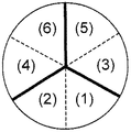
- FIG. 3B is a view when the corner cube prism 116 is viewed from the direction of incident light, and different polarization disturbances occur in the regions (1), (2), (3), (4), (5), and (6) shown here. appear.
- the bold line in the figure represents the boundary line between the reflecting surfaces.
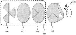
- a polarization compensation element 117 composed of a three-divided phase plate 501, a ⁇ / 4 plate 502, and a six-divided ⁇ / 2 plate 503 may be inserted.
- the ⁇ / 4 plate and the 6-divided ⁇ / 2 plate not only compensate for the polarization, but also have a function of rotating the polarization of the return light by 90 degrees with respect to the incident light.
- the three-divided phase plate generates a predetermined phase difference ⁇ p ⁇ s ( ⁇ p and ⁇ s are phases generated in horizontal polarization and vertical polarization, respectively) between horizontal polarization and vertical polarization in a specific region. It has the role of compensating for the phase difference between the region that passes through the element and the region that does not pass through, and aligning the wavefront of the return light.
- Table 1 shows set values of a three-divided phase plate, a ⁇ / 4 plate, and a six-divided ⁇ / 2 plate when the wavelength of light is 405 nm and the medium of the corner cube prism 116 is BK7.
- the angle is defined such that the vertical polarization direction 504 is 0 degree and the counterclockwise direction is positive when viewed from the incident light direction.
- Es is an electric field of signal light
- Er is an electric field of reference light
- the first component of the vector represents horizontal polarization
- the second component represents vertical polarization.
- This light is split into transmitted light and reflected light by a non-polarizing beam splitter 118, and the transmitted light passes through a ⁇ / 2 plate 119 having a fast axis in the direction of 22.5 degrees when viewed from the horizontal polarization direction. .
- Jones vector is
- the light reflected by the non-polarizing beam splitter 118 passes through a ⁇ / 4 plate 123 having a fast axis in the direction of 45 degrees as viewed from the horizontal polarization direction.
- Jones vector is
- the detection signals of the four detectors 121, 122, 125, 126 are respectively
- ⁇ is the conversion efficiency of the detector.
- ⁇ is the difference between the phase of the signal light and the phase of the reference light, that is, the interference phase. If these are respectively A1, A2, A3, A4, the differential signals D1, D2 are respectively
- the electric field Es of the signal light is amplified by the electric field Er of the reference light. Therefore, even if the Es is small due to the low reflectivity of the optical disk and the signal cannot be reproduced correctly even if the signal light is detected directly, the signal can be amplified and reproduced correctly.
- the interference phase ⁇ varies with time.
- the interference phase ⁇ is between the optical path length difference ⁇ L and the wavelength ⁇ of the light source.
- the optical path length difference In order to keep the interference phase constant, the optical path length difference must be suppressed to an accuracy sufficiently smaller than the wavelength of the light source, that is, within about 10 nanometers. As described above, the optical path length difference is adjusted to be zero by the actuator 107 and the movable portion 114. However, in the control of the actuator by a normal defocus signal, an error of several tens of nanometers is present in the focal position as a residual. In addition to the remaining (no problem when acquiring a normal reproduction signal), an extra optical path length difference occurs due to a slight tilt of the actuator during control, or an optical path length difference error due to an optical disc cover layer thickness error. Usually, an error of about several ⁇ m remains.
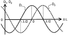
- FIG. 5 shows changes in D1 and D2 with respect to the optical path length difference.
- ⁇ L 0 at which D1 (RF signal) is maximum
- D2 is zero, which is an S-shaped curve just like a focus error signal or a track error signal.
- the interference phase can be controlled by using this signal as a phase error signal and performing closed loop control (hereinafter referred to as phase servo) so as to be always zero.
- phase servo closed loop control
- this error signal is fed back to the drive voltage 129 of the piezo element and the mirror 130 is moved in the front-rear direction to control the optical path length (interference phase).
- the optical path length difference when the optical path length difference is shifted to a positive value, the driving voltage of the piezo element increases, the mirror is pushed forward, the optical path length of the signal light is shortened, and the optical path length difference is in the negative direction. Conversely, when the optical path length difference moves in the negative direction, the optical path length difference moves in the positive direction. In this way, the interference phase can be kept at zero, and a stable amplified signal can be obtained.
- a is a signal amplification factor in the differential signal D1
- r, b1, b2, and ⁇ are constants indicating the characteristic error amount of the optical head optical system itself
- r is the differential signal D1 and the differential signal D2.
- Ratio of the maximum amplitude of each fluctuation component included in 1 b1 is a DC signal component included in the differential signal D1
- b2 is a DC signal component included in the differential signal D2
- ⁇ is the order of the differential signals D1 and D2. It is a phase difference.
- the differential signal outputs D1 and D2 of the optical head including the above error amount are expressed as shown in FIG.
- (1) in the figure represents the offset error (b2)
- D2 takes a non-zero value in the phase where D1 takes the maximum value. Therefore, if the phase servo is driven as it is, the phase is not locked to an appropriate phase, and the amplification factor of the reproduction signal decreases. .
- an offset is given to D2, so that D2 becomes zero at a position where the phase difference is zero. Note that offset and gain errors also occur in D1, but can be sufficiently removed by a signal processing system equivalent to the conventional one.
- the square of the output of this method may be treated as a reproduction signal.
- the reproduction signal output is proportional to the signal light intensity, as in the case of conventional optical disc signals such as DVD and Blu-ray disc, a conventional signal processing system can be used.
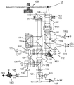
- FIG. 7 shows an example of the configuration of an optical disc apparatus when the detection optical system of the optical head is configured using three detectors.
- other components such as a signal processing circuit and a processor are the same as those of the optical disc apparatus shown in FIG.
- the phase difference between the signal light and the reference light is 0 degrees, 120 degrees, and 240 degrees on each detector, respectively.
- the light that has passed through the condenser lens 113 is divided into three light beams by non-polarizing beam splitters 701 and 702, and after passing through polarizers 703, 704, and 705 that transmit 45-degree polarized light, respectively, detectors 706, 707, 708 is detected.
- detectors 706, 707, 708 is detected.
- a phase plate 709 that generates a first phase difference between the signal light and the reference light
- the other is a second phase difference between the signal light and the reference light.
- Each of the phase plates 710 to be generated is inserted.
- the phase plate is set so that the first phase difference is 60 degrees and the second phase difference is ⁇ 60 degrees.
- the phase difference is a signed magnitude of the phase of the vertical polarization component with respect to the phase of the horizontal polarization component generated in the phase plate.
- the non-polarizing beam splitter 701 has a ratio of transmittance to reflectance of 1: 2, and the non-polarizing beam splitter 702 has the same transmittance and reflectance so that the amount of light on each detector is equal. Use things.
- the detector 708 has interference light having no phase difference between the signal light and the reference light
- the detector 706 has interference light having the first phase difference
- the detector 710 has Interfering light having a second phase difference is input.
- the intensity of the interference light having no phase difference is I1
- the intensity of the interference light having the first phase difference is I2
- the intensity of the interference light having the second phase difference is I3, I1, I2 and I3 can be expressed as follows.
- the differential signal represented by Equation 21 is a signal obtained by subtracting the interference light intensity output with a phase difference of 180 degrees from the average value of the interference light intensity output with the first phase difference and the interference light intensity output with the second phase difference.
- the differential signal represented by Equation 22 is obtained by multiplying the difference signal between the interference light intensity output having the first phase difference and the interference light intensity output having the second phase difference by ⁇ 3 / 2. is there.
- the same effect can be obtained by using D1 as the reproduction signal and D2 as the phase error signal as described above.
- the same effect can be obtained even with a smaller number of detector points. Since an error caused by an optical head assembly error or the like is superimposed on the differential signal detected by the actual optical system, the signal processing may be performed by performing the offset processing described with reference to FIG.
- FIG. 8 shows still another configuration example of the interference optical system and the detection optical system.
- the components other than the optical head are the same as those of the optical disk apparatus shown in FIG.
- a mirror 801 and a condensing lens 802 that condenses the incident light beam on the mirror are used as reference light reflecting means instead of the corner cube prism 116 and the polarization compensating element 117. It is installed. Even with such a configuration, similarly to the corner cube prism 116, it is possible to suppress the degradation of the interference signal amplitude due to the tilt of the element.
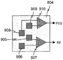
- an optical system for obtaining an interference signal includes an interference optical element 803 and a detector 804.
- the interference optical element 803 includes a non-polarization diffraction element 901, an anisotropic medium 902, and a Wollaston prism 903.
- the incident signal light is vertically polarized light and the reference light is horizontally polarized light
- the incident light is first divided into zero-order light and first-order light by the non-polarization diffraction grating 901 and is incident on the anisotropic medium 902.
- the first-order diffracted light is emitted with its direction changed in the horizontal direction with respect to the incident light.
- the optical axis of the anisotropic medium faces the traveling direction of the 0th-order light, only the 1st-order diffracted light has a delay between the signal light and the reference light, and the delay is ⁇ / 2 (the optical path length difference).
- the thickness of the medium is set so that ⁇ / 4).
- the non-polarization diffraction grating 901, the anisotropic medium 902, and the Wollaston prism 903 have the same functions as the half beam splitter 118, the ⁇ / 4 plate 123, and the polarization beam splitter 120, respectively.
- the detector Details of the detector are as shown in FIG. 9B.
- the light receiving units 905, 906, 907, and 908 correspond to the detectors 121, 122, 125, and 126 shown in FIG. 1, respectively, and a reproduction signal and a phase error signal are obtained by the differential circuits 907 and 910, respectively.
- the differential circuits 907 and 910 are incorporated in the detector 904, and the output of the difference between the detection currents of the light receiving unit by the differential circuit is converted into a voltage signal by the transimpedance amplifier.
- the optical path length difference control mechanism for executing the optical path length difference fixed position adjustment may be arranged on the reference light optical path instead of the reflected light optical path of the interference optical system as shown in FIG.
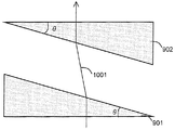
- FIG. 10 shows a configuration example in which a pair of wedge-shaped prisms 1001 and 1002 is arranged between the aberration correction element 117 mounted on the two-dimensional actuator 107 and the polarization beam splitter 104 as a control mechanism for the optical path length difference. .
- the phase error signal is fed back to the set of wedge-shaped prisms 1001 and 1002 via a servo circuit 79 (not shown), and phase control is executed.
- FIG. 10 shows a configuration example in which a pair of wedge-shaped prisms 1001 and 1002 is arranged between the aberration correction element 117 mounted on the two-dimensional actuator 107 and the polarization beam splitter 104 as a control mechanism for the optical path length difference.
- the phase error signal is fed back to the set of wedge-shaped prisms 1001 and 1002 via
- FIG. 11 shows a relative arrangement relationship between the pair of wedge-shaped prisms 1001 and 1002.
- One prism (prism 1002 in this embodiment) is mounted on the actuator 1003, and the optical path length can be controlled by moving the actuator in the optical axis direction.
- the optical path length can also be controlled by moving the actuator in a direction perpendicular to the optical axis (left and right direction with respect to the paper surface).
- the inclination angles of wedge prisms 1001 and 1002 see FIG.
- FIG. 13 and FIG. 14 show another configuration example of the optical path length difference coarse adjustment mechanism.
- the corner cube prism 116 is mounted on the same actuator as the objective lens 108 as a rough adjustment mechanism for the optical path length difference.
- the defocus signal FES detected by the detector 111 is input to both the two-dimensional actuator 107 and the actuator 1301 on which the corner cube prism 116 is mounted via the servo circuit 79, whereby the optical path length.
- a rough adjustment of the difference can be realized.
- the configuration shown in FIG. 13 can reduce the weight load on the actuator alone as compared with the configurations shown in FIGS.
- FIG. 14 shows a configuration in which the movable portion 114 and the prism mirror 115 are omitted from the configuration shown in FIG.
- the optical path length difference fixed position adjustment is executed by the actuator 1301.
- a signal obtained by adding a DC component to the defocus signal may be input, and the optical path length difference fixed position may be adjusted by changing the magnitude of the DC component.
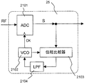
- FIG. 20 shows a specific example of the circuit block configuration of the signal processing circuit 25.
- the reproduction signal RF is digitized by the AD conversion circuit 2101 to obtain a digital signal output S.
- the digital signal output S and the output of the voltage controlled variable frequency oscillator (VCO) 2102 are phase-compared by the phase comparator 2103, and the output of the phase comparator is averaged by the low-pass filter (LPF) 2104. And fed back to the control input of the VCO.
- VCO voltage controlled variable frequency oscillator
- a phase-controlled clock output (CK) is obtained by a phase-locked loop (PLL) circuit constituted by a phase comparator 2103, a VCO 2102, and an LPF 2104, and AD conversion timing is controlled.
- the digital reproduction signal S is input to the demodulation circuit 24 and the address detection circuit 23 after appropriate digital equalization processing, and sent to the memory 29 and the microprocessor 27 as user data by the decoding circuit 26.
- the microprocessor controls the servo circuit 79 and the automatic position control means 76 according to an instruction from the host device 99, and positions the light spot 37 at an arbitrary address.
- the microprocessor 27 controls the laser driver 28 depending on whether the instruction from the host device is reproduction or recording, and causes the laser 101 to emit light with an appropriate power / waveform.
- the beam expander 1101 and the movable unit 114 are moved in the optical axis direction and fixed at a position where the signal quality is the best.
- the servo circuit 79 controls the two-dimensional actuator 107 based on the defocus signal and the track shift signal, and is focused on the recording surface of the optical disc 109 so as to follow the recording track. Further, the piezo element 801 is controlled based on the phase error signal generated from the differential circuit 128 so that the interference phase becomes zero.
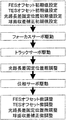
- FIG. 21 is a flowchart showing an example of a procedure for controlling the movable part and the actuator.
- coarse adjustment is performed for the defocus signal, the track shift signal, the optical path length difference fixed position, and the spherical aberration correction amount (the order is arbitrary). It is only necessary to remove the electrical offset for the focus error signal and the track error signal, and the optical path length difference fixed position and the spherical aberration correction amount should be set to specific values according to the type of disk, the layer number to be reproduced, and the like. Good.
- the focus servo and the track servo are driven in this order based on the focus error signal and the track error signal.
- the optical path length difference is adjusted by driving the movable portion 114 so that the amplitude of the phase error signal is maximized (optical path length difference fixed position coarse adjustment).
- the phase servo is driven based on the phase error signal. Since the playback signal stabilized at this point can be acquired, the focus error signal offset, the track error signal offset, the optical path length difference fixed position, and the spherical aberration correction amount are respectively monitored while finally monitoring the reproduction signal quality. A position where the reproduction signal quality is the best is searched, learned and set (FES offset fine adjustment, TES offset fine adjustment, optical path length fixed position fine adjustment, spherical aberration correction fine adjustment).
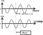
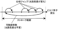
- phase jump As described below, the phase error signal when the optical path length difference changes is as shown in FIG.
- the black circle in the figure is the position of phase zero, and is fixed to one of these during phase servo driving. At this time, the position of the adjacent black circle can be moved by changing the optical path length difference by an amount corresponding to the period of the position error signal PES (hereinafter referred to as phase jump).
- the control is realized by supplying a phase jump signal for generating a phase jump to a fine adjustment means (for example, the mirror 130 and the piezo element 129 in FIG. 1) of the optical path length difference.
- the phase jump signal is composed of a movement pulse for moving to a target position and a braking pulse for stopping movement near the target position, and is generated by a servo signal circuit. Therefore, since it is possible to move to an arbitrary phase zero position by the phase jump, it is only necessary to search, learn and set a place where the reproduction signal quality is the best.
- Such search operation or learning operation is executed by the memory 28, the microprocessor 27, and the servo circuit 79.
- the servo circuit 79 supplies a phase jump signal to the optical path length fixed position adjusting means or the optical path length difference fine adjusting means, and the optical path length fixed position adjusting means or the optical path length difference fine adjusting means is used for the optical head optical system according to the phase jump signal.
- the optical path length is changed by a predetermined amount.
- the phase jump signal is preset in the phase servo circuit 79 so that the optical path length difference jumps by about the wavelength of the light source. Therefore, the phase servo is driven again immediately after the phase jump is completed, and the optical path length difference is fixed at a position shifted by exactly one wavelength.
- the phase jump is not limited to one wavelength, and a phase jump signal that jumps by an integral multiple of the wavelength, such as two wavelengths, may be used.
- This embodiment is premised on reproduction of a normal optical disc such as a DVD or a Blu-ray disc, but the form is not particularly limited as long as the incident light and the modulated signal light are coherent and have the same wavelength.
- the present invention can be applied to a large capacity memory such as a hologram memory or a near field memory.
- the optical disk apparatus includes the optical disk apparatus having the function of adjusting the fluctuation of the optical path length of the optical pickup optical system and the mechanism necessary for realizing the function, and a stable amplified signal for this purpose.
- An optical pickup capable of obtaining the above is realized.
- FIG. 15 shows a configuration example of an optical disc apparatus in which the optical path length difference fixed position adjustment and the phase servo are performed by the same movable part.
- FIG. 15 shows only the optical system and actuator of the optical head, the optical disc, and the optical disc support mechanism among the components of the optical disc, and the components common to FIG. 1 are not shown.
- the reproduction signal processing block 2 the microprocessor 27, the servo circuit 79, and the like are included in the same configuration example as in FIG.
- the prism mirror 115 shown in FIG. 1 is mounted on the actuator 1501, and a predetermined DC component instructed from the microprocessor 27 to the servo circuit 79 is added to the phase error signal as a drive current of the actuator 1501.
- the position of the optical path length difference is adjusted by adjusting the value of the DC component, and the phase servo is driven using the phase error signal component.
- the magnitude of the DC component is determined to be a predetermined value in accordance with the different layers of the multilayer optical disk, the type of the optical disk, and the like, in the same way as the movement amount of the actuator 1501 given to the movable unit 114 of the first embodiment. That is, adjusting the value of the DC component plays the role of adjusting the optical path length difference fixed position, like the movement amount adjustment of the movable portion 114 in the first embodiment.
- FIG. 16 shows a configuration example of an optical disc apparatus having a function of performing phase servo by the three-dimensional actuator 1601.
- the three-dimensional actuator 1601 is an actuator capable of controlling the tilt in the optical axis direction in addition to a normal two-dimensional actuator. Since the optical path length difference between the signal light and the reference light changes due to the inclination in the optical axis direction, the phase servo is driven by feeding back the phase error signal PES to the inclination in the optical axis direction.
- the configuration and function of the optical system for generating the phase error signal PES are the same as those in FIG.
- FIG. 17 shows a configuration example of an optical disc apparatus having a function of performing rough adjustment, fixed position adjustment, and fine adjustment of the optical path length difference with the same element.
- the actuator on which the objective lens 108 and the corner cube prism 116 are mounted is constituted by a three-dimensional actuator 1601, and in addition to driving in the XYZ directions, the mounted optical element is moved with respect to the optical axis. Movable to tilt.
- the coarse adjustment operation of the optical path length is executed by the movement of the three-dimensional actuator 1601 in the Z direction, and the fixed position adjustment and the fine adjustment operation are performed by the rotation operation about the X direction or the Y direction as the rotation axis. This is executed by changing the inclination of the prism 116 with respect to the optical axis.
- the three-dimensional actuator 1601 is controlled by the servo circuit 79. As a control signal for adjusting the tilt in the optical axis direction, a phase error signal current added with a DC current for adjusting the optical path length difference fixed position as an offset is input.
- This embodiment is a configuration example in the case where the reflectance and transmittance of the non-polarizing beam splitter 118 of the optical disc apparatus of Embodiment 1 are different.
- the non-polarizing beam splitter 118 in the first embodiment is a general one (half beam splitter) having the same reflectance and transmittance. Since the differential signal D1 includes a reproduction signal component, the detectors 121 and 122 need a sufficient band for acquiring the reproduction signal. On the other hand, since the differential signal D2 needs to have the reproduction signal component cut off, the detectors 124 and 125 require a narrower band than the detectors 121 and 122.
- the detectors 124 and 125 can set the amplifier gain of the detector relatively high, and as a result, the required optical signal. Is relatively small. That is, the amplitude of the reproduction signal can be increased by setting the transmittance of the non-polarizing beam splitter 118 to be larger than the reflectance. For example, assuming that a Blu-ray disc is played back at 4 ⁇ speed, the reproduction signal needs a bandwidth of about 100 MHz and the phase error signal of about 200 kHz, so the reflectance of the non-polarizing beam splitter is set to about 1% of the transmittance. It is enough.
- the signal amplification effect can be further increased, and the performance of the optical disc apparatus can be further improved.
- FIG. 18 shows a configuration example of an optical disc apparatus having the functions of this embodiment. Since the phase error signal is obtained by removing the reproduction signal component from the detection signal, even if the light emission power of the light source is constant, the amplitude varies depending on whether it is a recorded portion or an unrecorded portion, or the depth of modulation. For this reason, in this embodiment, a part of the signal light is extracted by being reflected by a special polarizing beam splitter 1801 (equivalent to the special polarizing beam splitter 105) arranged on the optical path for generating the signal light, and collected.
- a special polarizing beam splitter 1801 equivalent to the special polarizing beam splitter 105
- An optical lens 1802 is used to guide the detector 1803 to output an average power signal G.
- the output average power signal G is input to a division circuit 1804 arranged at the subsequent stage of the differential detector 128.
- the output D2 of the differential detector 128 corresponds to a phase error signal.
- the division circuit 1804 executes arithmetic processing for dividing (normalizing) the phase error signal by the average power signal. As a result, a phase error signal having a constant amplitude independent of the state of the optical disk can be obtained, and stable phase servo driving can be performed.
- FIG. 18 the configuration example in which the optical branch and the detector for obtaining the average power signal G are newly provided has been described. However, even if the output is obtained using the output signal of the detector 111 as shown in FIG. Good. In this case, the total output A + B + C + D of the light receiving units 201, 202, 203, 204 shown in FIG. 2 (however, the reproduction signal component is dropped due to band limitation) is the average power signal G. Accordingly, in FIG. 19, in addition to the configuration of FIG. 2, the quadrant detector provided with the logic circuit element for calculating the sum A + B + C + D of the outputs of the light receiving units 201, 202, 203, 204 is It is installed as an acquisition means.
- an optical disc apparatus and an optical head capable of stable phase servo drive can be realized as compared with the configurations shown in Embodiments 1 to 5.
- This embodiment is a case where the optical path length difference fixed position fine adjustment in the first embodiment is performed by a combination of the piezo element 129 and the movable portion 114. Specifically, as shown in FIG. 23, the movable portion is moved when reaching the end of the stroke range of the piezo element by repeating the phase jump. Then, since closed-loop control is performed, the piezo element expands and contracts (in conjunction with the movable part) without changing the optical path length difference, so that it is possible to perform further phase jumps. It is possible to repeat the phase jump within the stroke range. That is, even when the stroke of the piezo element 129 is short, a sufficient optical path length difference adjustment range can be ensured.
- the piezoelectric element preferably has a shorter length in the expansion / contraction direction.
- the length in the expansion / contraction direction is proportional to the stroke of the piezoelectric element, the response speed and the stroke are in a trade-off relationship. Therefore, with this configuration, it is possible to secure a response speed of the piezo element by allowing a short stroke, and to contribute to an increase in the reproduction speed of the optical disc apparatus. Moreover, since it has the effect of reducing the size of the piezo element, it can contribute to the downsizing of the optical disk device, particularly the optical head unit.
- the present invention makes it possible to detect a reproduction signal of a large-capacity multilayer high-speed optical disk stably and with high quality, and a wide range of industrial applications such as a large-capacity video recorder, a hard disk data backup device, and a storage information archive device can be expected.
Landscapes
- Physics & Mathematics (AREA)
- Optics & Photonics (AREA)
- Optical Recording Or Reproduction (AREA)
- Optical Head (AREA)
Applications Claiming Priority (2)
| Application Number | Priority Date | Filing Date | Title |
|---|---|---|---|
| JP2009060420A JP5452040B2 (ja) | 2009-03-13 | 2009-03-13 | 光学的情報再生方法、光ヘッドおよび光ディスク装置 |
| JP2009-060420 | 2009-03-13 |
Publications (1)
| Publication Number | Publication Date |
|---|---|
| WO2010103962A1 true WO2010103962A1 (ja) | 2010-09-16 |
Family
ID=42728252
Family Applications (1)
| Application Number | Title | Priority Date | Filing Date |
|---|---|---|---|
| PCT/JP2010/053387 Ceased WO2010103962A1 (ja) | 2009-03-13 | 2010-03-03 | 光学的情報再生方法、光ヘッドおよび光ディスク装置 |
Country Status (2)
| Country | Link |
|---|---|
| JP (1) | JP5452040B2 (https=) |
| WO (1) | WO2010103962A1 (https=) |
Cited By (6)
| Publication number | Priority date | Publication date | Assignee | Title |
|---|---|---|---|---|
| JP2012027996A (ja) * | 2010-07-28 | 2012-02-09 | Hitachi Consumer Electronics Co Ltd | 光情報記録再生装置及び再生装置 |
| JP2012069189A (ja) * | 2010-09-22 | 2012-04-05 | Sony Corp | 再生装置、光路長サーボ制御方法 |
| JP2012174290A (ja) * | 2011-02-17 | 2012-09-10 | Hitachi Media Electoronics Co Ltd | 光ピックアップ装置および光ディスク装置 |
| WO2014188532A1 (ja) * | 2013-05-22 | 2014-11-27 | 日立コンシューマエレクトロニクス株式会社 | 光情報再生装置 |
| WO2016120924A1 (ja) * | 2015-01-30 | 2016-08-04 | ソニー株式会社 | 再生装置および再生方法 |
| CN109089113A (zh) * | 2018-10-12 | 2018-12-25 | 四川长虹电器股份有限公司 | 一种平板电视的自动进行重显率调整的方法 |
Families Citing this family (5)
| Publication number | Priority date | Publication date | Assignee | Title |
|---|---|---|---|---|
| JP5309008B2 (ja) | 2009-12-15 | 2013-10-09 | 日立コンシューマエレクトロニクス株式会社 | 光情報記録再生装置および光情報再生装置 |
| JP5409479B2 (ja) | 2010-03-29 | 2014-02-05 | 日立コンシューマエレクトロニクス株式会社 | 光情報再生装置、光情報記録装置及び情報記録方法 |
| JP5758728B2 (ja) | 2011-07-26 | 2015-08-05 | 株式会社日立ハイテクノロジーズ | 荷電粒子線装置 |
| JP2013033572A (ja) * | 2011-08-03 | 2013-02-14 | Sony Corp | 光ピックアップ装置、再生装置 |
| JP7017985B2 (ja) | 2018-06-05 | 2022-02-09 | 株式会社日立製作所 | システム及び処理条件の決定方法 |
Citations (6)
| Publication number | Priority date | Publication date | Assignee | Title |
|---|---|---|---|---|
| JP2007317284A (ja) * | 2006-05-25 | 2007-12-06 | Hitachi Ltd | 光ディスク装置 |
| JP2008065961A (ja) * | 2006-09-11 | 2008-03-21 | Hitachi Ltd | 光情報検出方法、光ヘッド及び光ディスク装置 |
| JP2008243273A (ja) * | 2007-03-27 | 2008-10-09 | Hitachi Ltd | 光ヘッド及び光情報記録媒体の再生方法 |
| JP2008269680A (ja) * | 2007-04-18 | 2008-11-06 | Hitachi Ltd | 光ヘッドおよび光ディスク装置 |
| JP2008310942A (ja) * | 2007-02-23 | 2008-12-25 | Hitachi Ltd | 光ヘッドおよび光ディスク装置 |
| JP2009252337A (ja) * | 2008-04-11 | 2009-10-29 | Hitachi Ltd | 光ヘッド及び光ディスク装置 |
-
2009
- 2009-03-13 JP JP2009060420A patent/JP5452040B2/ja not_active Expired - Fee Related
-
2010
- 2010-03-03 WO PCT/JP2010/053387 patent/WO2010103962A1/ja not_active Ceased
Patent Citations (6)
| Publication number | Priority date | Publication date | Assignee | Title |
|---|---|---|---|---|
| JP2007317284A (ja) * | 2006-05-25 | 2007-12-06 | Hitachi Ltd | 光ディスク装置 |
| JP2008065961A (ja) * | 2006-09-11 | 2008-03-21 | Hitachi Ltd | 光情報検出方法、光ヘッド及び光ディスク装置 |
| JP2008310942A (ja) * | 2007-02-23 | 2008-12-25 | Hitachi Ltd | 光ヘッドおよび光ディスク装置 |
| JP2008243273A (ja) * | 2007-03-27 | 2008-10-09 | Hitachi Ltd | 光ヘッド及び光情報記録媒体の再生方法 |
| JP2008269680A (ja) * | 2007-04-18 | 2008-11-06 | Hitachi Ltd | 光ヘッドおよび光ディスク装置 |
| JP2009252337A (ja) * | 2008-04-11 | 2009-10-29 | Hitachi Ltd | 光ヘッド及び光ディスク装置 |
Cited By (9)
| Publication number | Priority date | Publication date | Assignee | Title |
|---|---|---|---|---|
| JP2012027996A (ja) * | 2010-07-28 | 2012-02-09 | Hitachi Consumer Electronics Co Ltd | 光情報記録再生装置及び再生装置 |
| JP2012069189A (ja) * | 2010-09-22 | 2012-04-05 | Sony Corp | 再生装置、光路長サーボ制御方法 |
| JP2012174290A (ja) * | 2011-02-17 | 2012-09-10 | Hitachi Media Electoronics Co Ltd | 光ピックアップ装置および光ディスク装置 |
| WO2014188532A1 (ja) * | 2013-05-22 | 2014-11-27 | 日立コンシューマエレクトロニクス株式会社 | 光情報再生装置 |
| WO2016120924A1 (ja) * | 2015-01-30 | 2016-08-04 | ソニー株式会社 | 再生装置および再生方法 |
| JPWO2016120924A1 (ja) * | 2015-01-30 | 2017-11-09 | ソニー株式会社 | 再生装置および再生方法 |
| US9916856B2 (en) | 2015-01-30 | 2018-03-13 | Sony Corporation | Playing apparatus and playing method |
| CN109089113A (zh) * | 2018-10-12 | 2018-12-25 | 四川长虹电器股份有限公司 | 一种平板电视的自动进行重显率调整的方法 |
| CN109089113B (zh) * | 2018-10-12 | 2019-09-10 | 四川长虹电器股份有限公司 | 一种平板电视的自动进行重显率调整的方法 |
Also Published As
| Publication number | Publication date |
|---|---|
| JP2010218591A (ja) | 2010-09-30 |
| JP5452040B2 (ja) | 2014-03-26 |
Similar Documents
| Publication | Publication Date | Title |
|---|---|---|
| JP5452040B2 (ja) | 光学的情報再生方法、光ヘッドおよび光ディスク装置 | |
| JP5153424B2 (ja) | 光ヘッド及び光ディスク装置 | |
| JP5081763B2 (ja) | 光情報検出方法、光ピックアップ及び光情報記録再生装置 | |
| JP4861948B2 (ja) | 光ヘッドおよび光ディスク装置 | |
| JP4564948B2 (ja) | 光情報検出方法、光ヘッド及び光ディスク装置 | |
| KR100841836B1 (ko) | 광 디스크 장치 | |
| US20120188618A1 (en) | Optical information reproducing method and optical information reproducing apparatus | |
| JP2008269680A (ja) | 光ヘッドおよび光ディスク装置 | |
| JP5043049B2 (ja) | 光学的情報再生方法及び光ディスク装置 | |
| US7764576B2 (en) | Optical information recording and reproducing apparatus | |
| JP2008243273A (ja) | 光ヘッド及び光情報記録媒体の再生方法 | |
| US20120008483A1 (en) | Optical head and optical disc apparatus | |
| JP2007193894A (ja) | 光記録再生装置、光学ピックアップ及びトラッキングエラー信号検出方法 | |
| JP5780932B2 (ja) | 光情報記録再生装置、光情報記録装置 | |
| JP6158339B2 (ja) | ホログラム再生装置、ホログラム再生方法 | |
| US20070297731A1 (en) | Optical pick-up | |
| JP5468033B2 (ja) | 光情報再生装置及び光情報記録再生装置 | |
| JP2007323791A (ja) | 光情報記録再生装置 | |
| US20110002117A1 (en) | Optical disc drive | |
| JP5778624B2 (ja) | 光情報再生装置及び光情報再生方法 | |
| JP2007250034A (ja) | 光ピックアップ用受光素子の位置調整方法 | |
| US20170236543A1 (en) | Optical information recording/reproducing device and holographic recording/reproducing method | |
| WO2013183439A1 (ja) | 光ピックアップ装置 | |
| JP2012138133A (ja) | 光ピックアップ装置及び光ディスク装置 | |
| JP2008305493A (ja) | 光学式情報記録再生装置 |
Legal Events
| Date | Code | Title | Description |
|---|---|---|---|
| 121 | Ep: the epo has been informed by wipo that ep was designated in this application |
Ref document number: 10750716 Country of ref document: EP Kind code of ref document: A1 |
|
| NENP | Non-entry into the national phase |
Ref country code: DE |
|
| 122 | Ep: pct application non-entry in european phase |
Ref document number: 10750716 Country of ref document: EP Kind code of ref document: A1 |