WO2010095504A1 - 薄膜トランジスタの製造方法 - Google Patents
薄膜トランジスタの製造方法 Download PDFInfo
- Publication number
- WO2010095504A1 WO2010095504A1 PCT/JP2010/051340 JP2010051340W WO2010095504A1 WO 2010095504 A1 WO2010095504 A1 WO 2010095504A1 JP 2010051340 W JP2010051340 W JP 2010051340W WO 2010095504 A1 WO2010095504 A1 WO 2010095504A1
- Authority
- WO
- WIPO (PCT)
- Prior art keywords
- film transistor
- liquid repellent
- thin film
- semiconductor
- film
- Prior art date
- Legal status (The legal status is an assumption and is not a legal conclusion. Google has not performed a legal analysis and makes no representation as to the accuracy of the status listed.)
- Ceased
Links
Images





Classifications
-
- H—ELECTRICITY
- H10—SEMICONDUCTOR DEVICES; ELECTRIC SOLID-STATE DEVICES NOT OTHERWISE PROVIDED FOR
- H10K—ORGANIC ELECTRIC SOLID-STATE DEVICES
- H10K71/00—Manufacture or treatment specially adapted for the organic devices covered by this subclass
- H10K71/10—Deposition of organic active material
- H10K71/12—Deposition of organic active material using liquid deposition, e.g. spin coating
Definitions
- the present invention relates to a method for manufacturing a thin film transistor, and more particularly to a method for manufacturing a thin film transistor having a semiconductor protective film.
- TFT thin film transistor
- organic TFTs TFTs using organic materials
- organic materials have a wider choice of materials than inorganic materials, and in the manufacturing process of organic TFTs, instead of the vacuum process and high temperature process described above, processes with excellent productivity such as printing and coating are used. Manufacturing cost can be reduced.
- the organic TFT may be formed on a flexible substrate such as a plastic film having poor heat resistance, and is expected to be applied to various fields such as a curved display.
- a droplet coating technique such as an inkjet method or a dispenser method in which a solution (hereinafter also referred to as ink) in which an organic semiconductor material is dissolved or dispersed is directly applied to a substrate is known.
- ink a solution in which an organic semiconductor material is dissolved or dispersed is directly applied to a substrate.
- Patent Document 1 as a method for manufacturing an organic EL device, when a liquid droplet containing a light emitting material is applied, a liquid repellent treatment is performed on a substrate surface on which the liquid is to be placed. There has been proposed a method for preventing wet spreading from the application position.
- semiconductor materials especially organic semiconductor materials
- the present invention has been made in view of the above problems, and provides a method for manufacturing a thin film transistor that can accurately form a semiconductor film and a protective film at predetermined positions with an appropriate film thickness, and that is excellent in productivity.
- the purpose is to provide.
- a method for manufacturing a thin film transistor having a protective film for protecting a semiconductor film Forming a liquid repellent layer having higher liquid repellency than the predetermined region on the surface of the base layer so as to surround a predetermined region of the surface of the base layer; Applying the semiconductor solution to the predetermined region to form the semiconductor film; Reducing the liquid repellency of the liquid repellent layer after the semiconductor film is formed; And a step of applying a protective film material solution so as to cover the semiconductor film and forming a protective film after the liquid repellency of the liquid repellent layer is lowered.
- the thin film transistor has a bottom gate bottom contact structure
- the underlayer is a substrate on which a source electrode and a drain electrode are formed, 6.
- the thin film transistor has a bottom gate top contact structure,
- the foundation layer is a gate insulating film covering the gate electrode; 6.
- the thin film transistor has a top gate bottom contact structure
- the underlayer is a substrate on which a source electrode and a drain electrode are formed, 6.
- the thin film transistor has a top gate top contact structure
- the underlayer is a substrate on which a source electrode and a drain electrode are to be formed, 6.
- a semiconductor film and a protective film can be accurately formed at predetermined positions with appropriate thicknesses, and the semiconductor film can be sufficiently covered with the protective film, and the thin film transistor is excellent in productivity.
- the manufacturing method of can be provided.
- coating method It is a cross-sectional schematic diagram which shows schematic structure of TFT which concerns on embodiment of this invention. It is
- FIG. 7 a reference example in the case where a liquid repellent region is provided and an organic semiconductor film is formed and then a protective film is formed using a droplet coating method will be described.
- 7A to 7D the upper diagram is a schematic sectional view, and the lower diagram is a schematic plan view.
- a liquid repellent layer CF is formed on the base layer LF so as to surround the ink application region IA (FIG. 7A).
- the ink IK is applied to the ink application area IA (FIG. 7B) and dried to form the organic semiconductor film SF (FIG. 7C).
- a protective film material solution is applied on the organic semiconductor film SF to form a protective film PF (FIG. 7D).
- FIG. 7D the central portion A of the organic semiconductor film SF is sufficiently covered with the protective film PF, but the peripheral portion B is thinned by the influence of the liquid repellent layer CF.
- FIG.7 (e) is an enlarged view of the peripheral part B vicinity in FIG.7 (d). Therefore, the presence of the liquid repellent layer CF may prevent the organic semiconductor film SF from being sufficiently covered with the protective film PF.
- the protective film PF if the amount of the protective film material solution is increased in order to increase the thickness of the protective film PF, the protective film PF cannot stay in the place where the solution is applied, and flows out of the liquid repellent layer CF. As a result, the coating with the protective film PF cannot be sufficiently performed, and the organic semiconductor film SF cannot be sufficiently protected.
- FIG. 1 is a schematic cross-sectional view showing a schematic configuration of a TFT according to an embodiment of the present invention.
- 1A is a bottom gate bottom contact TFT 1
- FIG. 1B is a bottom gate top contact TFT 1
- FIG. 1C is a top gate bottom contact TFT 1
- FIG. 2 is a schematic cross-sectional view showing a schematic configuration of a gate top contact type TFT1.
- the TFT 1 includes a substrate P, a gate electrode G, a gate insulating film IF, a source electrode S, a drain electrode D, a semiconductor film SF, a protective film PF, and a liquid repellent. It is composed of a layer CF or the like.
- the gate insulating film IF functions as the protective film PF.
- polyimide polyamide
- PET polyethylene terephthalate
- PEN polyethylene naphthalate
- PES polyethersulfone
- a gate electrode material is formed on the substrate P by sputtering, vapor deposition or the like, and then photolithography is performed. It can be formed by patterning using a method. Further, it can be formed by using a mask vapor deposition method, a printing method, a droplet coating method, or the like.
- the material of the gate electrode G Al, Au, Ag, Pt, Pd, Cu, Cr, Mo, In, Zn, Mg, etc., alloys or oxides containing these, or organic conductors such as carbon nanotubes, etc. Can be used.
- the gate insulating film IF As a method for forming the gate insulating film IF, sputtering, vapor deposition, CVD, spin coating, ink jet, or the like can be used.
- a material of the gate insulating film IF inorganic oxides such as silicon oxide, aluminum oxide, tantalum oxide, and titanium oxide, and inorganic nitrides such as silicon nitride and aluminum nitride can be used.
- polyimide, polyamide, polyester, polyacrylate, photo-curing polymer of photo radical polymerization, photo cation polymerization, copolymer containing acrylonitrile component, organic compound such as polyvinyl phenol, polyvinyl alcohol, novolac resin, cyanoethyl pullulan Etc. can also be used.
- the source electrode S and the drain electrode D similarly to the method for forming the gate electrode G, it can be formed using a photolithography method, various printing methods, a droplet coating method, or the like.
- the electrode material of the source electrode S / drain electrode D the same electrode material as that of the gate electrode G can be used.
- the liquid repellent layer CF can be formed by forming a liquid repellent layer material using a spin coat method or the like and then patterning using a photolithography method. It can also be formed using a printing method, a droplet coating method, or the like. As will be described later, the liquid repellent layer CF is a region (ink coating) on which the semiconductor solution (ink IK) on the surface of the base layer (source electrode S / drain electrode D, gate insulating film IF, or substrate P) is to be applied. It is formed so as to surround the region IA). Further, the liquid repellent layer CF has higher liquid repellency than the ink application area IA with respect to the ink IK.
- the material of the liquid repellent layer CF a polymer material imparted with liquid repellency by a fluorine-based liquid repellent material, a silicone-based liquid repellent material, or the like can be used, and it has photosensitivity particularly in that pattern formation can be easily performed. It is preferable to use a resist material.
- the photosensitive resist material include acrylic, phenolic, polyimide, and PVA resins.
- the liquid repellent layer CF can be formed by applying a polymer material in a pattern by a printing method and then performing a liquid repellent treatment on the surface thereof.
- the liquid repellent treatment include plasma treatment in a gas atmosphere containing fluorine such as SF 4 , SF 6 , C 2 F 6 , and CHF 3 .
- the plasma treatment in this case may be performed under reduced pressure or under atmospheric pressure.
- a polymer material having a liquid repellent substituent instead of mixing the liquid repellent material with the polymer material as described above. May be used.
- the substituent having liquid repellency include a substituent having at least a part thereof substituted with fluorine, such as a fluoroalkyl group.
- an inkjet method in which a solution in which a semiconductor material is dissolved or dispersed is applied as droplets can be used.
- the material of the semiconductor film SF can be a polycyclic aromatic compound, a conjugated polymer, or the like, but is not particularly limited.
- a polymer material, an oligomer, or a low-molecular material may be used, and a material in which molecules are regularly arranged and formed into crystals by intermolecular interaction after coating is particularly preferable.
- Pentacene, porphyrin, phthalocyanine, oligothiophene, oligophenylene, polythiophene, polyphenylene, and derivatives thereof can be used.
- pentacene 6,13-bis (triisopropylsilylethynyl) pentacene, tetrabenzoporphyrin, poly (3-hexylthiophene), or the like can be used.
- an organic solvent can be used, for example, hydrocarbons such as toluene and xylene, alcohols such as methanol and ethanol, ketones such as acetone and methyl ethyl ketone, diethylene glycol monomethyl ether, and the like.
- Suitable solvents for semiconductor materials can be selected from ethers of the above, esters such as ethyl acetate and butyl acetate, and halogenated hydrocarbons such as chloroform and trichloroethylene.
- the protective film PF As a method for forming the protective film PF, an inkjet method can be used. As a material for the protective film PF, polyvinyl alcohol, 2-hydroxyethyl methacrylate (HEMA), acrylic acid, acrylamide, or the like can be used.
- HEMA 2-hydroxyethyl methacrylate
- an area (ink application area IA) to which the semiconductor solution (ink IK) is applied is formed.
- a liquid repellent layer CF having higher liquid repellency than the ink application area IA is formed on the ink IK.
- UV light ultraviolet
- immersion in a solvent ultrasonic treatment in a solvent, plasma treatment, or the like
- immersion in a solvent ultrasonic treatment in a solvent, plasma treatment, or the like
- processing method and the processing strength may be selected depending on the required degree of liquid repellency.
- liquid repellent layer CF When a polymer material mixed with a liquid repellent material is used as the liquid repellent layer CF, immersion in a solvent or ultrasonic waves in the solvent is particularly effective. In the case of using a polymer material having a liquid repellent substituent, cutting the polymer bond by plasma treatment is highly effective in reducing the liquid repellency. In addition, when using a polymer material having a liquid repellent treatment on the surface, a method using ultraviolet irradiation or immersion in a solvent is particularly effective.
- an organic solvent can be used as the solvent used for reducing the liquid repellency of the liquid repellent layer CF.
- hydrocarbons such as toluene and xylene, alcohols such as methanol and ethanol, acetone, Ketones such as methyl ethyl ketone, ethers such as diethylene glycol monomethyl ether, esters such as ethyl acetate, butyl acetate and ethyl benzoate, and halogenated hydrocarbons such as chloroform and trichloroethylene can be used.
- the liquid repellency can be lowered by using a solvent in which the mixed liquid repellent material is easily dissolved.
- the liquid repellency can be lowered by water.
- Example 1-1 An embodiment 1-1 of a manufacturing method of the bottom gate bottom contact type TFT 1 will be described with reference to FIG.
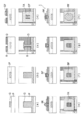
- FIG. 2A to FIG. 2H are schematic views showing the manufacturing process of the bottom gate bottom contact type TFT 1 in Example 1-1.
- the upper figure is a schematic sectional view and the lower figure is a schematic plan view.
- glass is used as the substrate P, and a Cr film is formed thereon with a thickness of 50 nm using a sputtering method, followed by patterning using a photolithography method to form a gate electrode G (FIG. 2A )).
- a SiO 2 film was formed using a TEOS • CVD method to form a gate insulating film IF having a thickness of 500 nm (FIG. 2B).
- a TEOS • CVD method to form a gate insulating film IF having a thickness of 500 nm (FIG. 2B).
- the gate electrode G is shown as a view through the gate insulating film IF.
- a photosensitive bank agent NPAR-502 manufactured by Nissan Chemical Co., Ltd .: acrylic resin added with a fluorosurfactant
- NPAR-502 manufactured by Nissan Chemical Co., Ltd .: acrylic resin added with a fluorosurfactant
- FIG. 2D the liquid repellent layer CF was formed so as to surround the channel region between the source electrode S and the drain electrode D.
- the liquid repellent property of the liquid repellent layer CF was lowered by irradiating the surface of the liquid repellent layer CF with UV light by a mask exposure method (FIG. 2 (g)).
- Example 1-2 of a method for manufacturing the bottom gate / bottom contact type TFT 1 will be described with reference to FIG.
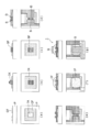
- FIG. 3A to FIG. 3H are schematic views showing a manufacturing process of the bottom gate bottom contact type TFT 1 in Example 1-2.
- the upper figure is a schematic sectional view and the lower figure is a schematic plan view.
- a Cr film is formed thereon with a thickness of 50 nm by sputtering, and then patterned by photolithography to form a gate electrode G (FIG. 3A )).
- an optomer PC403 which is a photosensitive acrylate material, was formed to form a gate insulating film IF having a thickness of 500 nm (FIG. 3B).
- the gate electrode G is shown as a view through the gate insulating film IF.
- patterning is performed by using a photolithography method to form a source electrode S and a drain electrode D (FIG. 3C). .
- a photosensitive bank agent NPAR-502 manufactured by Nissan Chemical Co., Ltd.
- NPAR-502 manufactured by Nissan Chemical Co., Ltd.
- the liquid repellent layer CF was formed so as to surround the channel region between the source electrode S and the drain electrode D.
- a tetrabenzoporphyrin precursor solution (ink IK) is applied to the region IA surrounded by the liquid repellent layer CF using an ink jet method (FIG. 3E), and heated and fired to form the semiconductor film SF. (FIG. 3 (f)).
- Example 2 of the manufacturing method of the bottom gate top contact type TFT 1 will be described with reference to FIG.
- FIG. 4A to FIG. 4H are schematic views showing a manufacturing process of the bottom gate top contact type TFT 1 in the second embodiment.
- the upper figure is a schematic sectional view and the lower figure is a schematic plan view.
- glass is used as the substrate P, and a Cr film is formed thereon with a thickness of 50 nm using a sputtering method, followed by patterning using a photolithography method to form a gate electrode G (FIG. 4A )).
- an optomer PC403 which is a photosensitive acrylate material, was formed to form a gate insulating film IF having a thickness of 500 nm (FIG. 4B). 4B and 4C, the gate electrode G is illustrated as a view through the gate insulating film IF.
- a photosensitive bank agent NPAR-502 manufactured by Nissan Chemical Industries, Ltd. was applied using a spin coat, and then patterned using a photolithography method to form a liquid repellent layer CF (FIG. 4 (c)). At this time, the liquid repellent layer CF was formed so as to surround a region corresponding to the gate electrode G formed in the lower layer.
- a Cr film was formed with a thickness of 5 nm and an Au film was formed with a thickness of 50 nm to form a source electrode S and a drain electrode D (FIG. 4F).
- the liquid repellent property of the liquid repellent layer CF was lowered by irradiating the surface of the liquid repellent layer CF with UV light by a mask exposure method (FIG. 4G).
- FIG. 5A to FIG. 5G are schematic views showing the manufacturing process of the top gate bottom contact type TFT 1 in the third embodiment.
- the upper figure is a schematic sectional view and the lower figure is a schematic plan view.
- glass is used as the substrate P, and a Cr film is formed thereon with a thickness of 5 nm and an Au film is formed with a thickness of 50 nm using a sputtering method, followed by patterning using a photolithography method, and then a source electrode S / drain electrode D was formed (FIG. 5A).
- a photosensitive bank agent NPAR-502 manufactured by Nissan Chemical Industries, Ltd. was applied using a spin coat, and then patterned using a photolithography method to form a liquid repellent layer CF (FIG. 5 (b)). At this time, the liquid repellent layer CF was formed so as to surround the channel region between the source electrode S and the drain electrode D.
- the liquid repellency of the liquid repellent layer CF was lowered by irradiating the surface of the liquid repellent layer CF with UV light using a mask exposure method (FIG. 5E).
- optomer PC403 which is a photosensitive acrylate material, was applied to the surface of the semiconductor film SF and heated to form the gate insulating film IF (FIG. 5F).
- the gate insulating film IF also serves as the protective film PF.
- a Cr film was formed with a thickness of 50 nm by using a mask vapor deposition method, a gate electrode G was formed, and the TFT 1 was completed (FIG. 5G).
- Example 4 Example 4 of the manufacturing method of the top gate top contact type TFT 1 will be described with reference to FIG. 6 (a) to 6 (g) are schematic views showing the manufacturing process of the top gate top contact type TFT 1 in Example 4.
- FIG. 6 (a) to 6 (g) are schematic views showing the manufacturing process of the top gate top contact type TFT 1 in Example 4.
- FIG. 6 (a) to 6 (g) are schematic views showing the manufacturing process of the top gate top contact type TFT 1 in Example 4.
- a photosensitive bank agent NPAR-502 manufactured by Nissan Chemical Co., Ltd.
- NPAR-502 manufactured by Nissan Chemical Co., Ltd.
- a photolithography method to form a liquid repellent layer CF.
- the liquid repellent layer CF was formed so as to surround a region corresponding to a channel region between the source electrode S and the drain electrode D formed in a later step.
- a tetrabenzoporphyrin precursor solution (ink IK) is applied to the region IA surrounded by the liquid repellent layer CF by using an ink jet method (FIG. 6B), and heated and fired to form the semiconductor film SF. (FIG. 6C).
- a Cr film was formed to a thickness of 5 nm and an Au film was formed to a thickness of 50 nm to form a source electrode and a drain electrode (FIG. 6D).
- optomer PC403 which is a photosensitive acrylate material, was applied to the surface of the semiconductor film SF and heated to form the gate insulating film IF (FIG. 6F).
- the gate insulating film IF also serves as the protective film PF.
- a Cr film was formed with a thickness of 50 nm by using a mask vapor deposition method, a gate electrode G was formed, and the TFT 1 was completed (FIG. 5G).
- the semiconductor film SF and the protective film PF were appropriate as in the case of Example 1. It was confirmed that the film was accurately formed at a predetermined position in terms of film thickness.
- the semiconductor solution (ink IK) and the protective film material solution are applied using a droplet application method typified by an ink jet method, productivity can be increased.
Landscapes
- Engineering & Computer Science (AREA)
- Manufacturing & Machinery (AREA)
- Thin Film Transistor (AREA)
Abstract
本発明は、半導体膜、及び保護膜を適正な膜厚で所定の位置に精度良く形成することができ、且つ、生産性の優れた薄膜トランジスタの製造方法を提供する。半導体膜を保護する保護膜を有する薄膜トランジスタの製造方法において、下地層の表面に、該下地層の表面の所定の領域を囲むように、半導体溶液に対し該所定の領域よりも高い撥液性を有する撥液層を形成する工程と、前記所定の領域に、半導体溶液を塗布し、半導体膜を形成する工程と、半導体膜が形成された後、撥液層の撥液性を低下させる工程と、撥液層の撥液性が低下された後、半導体膜を覆うように、保護膜材料溶液を塗布し、保護膜を形成する工程と、を有する。
Description
本発明は、薄膜トランジスタの製造方法に関し、特に半導体保護膜を有する薄膜トランジスタの製造方法に関する。
近年、基板上に薄膜トランジスタ(以下、TFTとも記す)を形成する技術が大幅に進歩し、特にアクティブマトリクス型の大画面表示装置の駆動素子への応用開発が進められている。現在実用化されているTFTは、半導体材料としてa-Siやpoly-SiといったSi系の無機材料を用いて製造されているが、このような無機材料を用いたTFTの製造においては、真空プロセスや高温プロセスを必要とし、製造コストに大きく影響を及ぼしている。
そこで、このような問題に対応する為、近年、有機材料を用いたTFT(以下、有機TFTとも記す)が種々検討されている。有機材料は無機材料に比べ、材料の選択肢が広く、また、有機TFTの製造工程においては、前述の真空プロセスや高温プロセスに代えて、印刷や塗布といった生産性に優れたプロセスが用いられる為、製造コストを抑えることができる。さらに、有機TFTは、耐熱性の乏しい、例えばプラスティックフィルム等の可撓性を有する基板にも形成することができる可能性があり、曲面ディスプレイ等多方面への応用が期待されている。
有機半導体材料の塗布方法としては、有機半導体材料を溶解又は分散した溶液(以下、インクとも記す)を基板に直接塗布するインクジェット法やディスペンサ法等の液滴塗布技術が知られている。これらの技術は、1.真空プロセスが不要、2.材料の浪費がない、3.直接パターニングできる為、フォトリソグラフィー法と比べてエッチング工程が不要、といった利点がある。
このような有機TFTにおいて、優れた電気特性と高い信頼性を得る為には、有機半導体膜を適正な膜厚で所定の位置に精度良く形成する必要がある。しかしながら、有機TFTの有機半導体膜を前述のインクジェット法やディスペンサ法等を用いて形成する際、塗布されたインクが乾燥し固形化するまでに基板の表面状態(撥液性・親液性)や乾燥雰囲気等の影響により濡れ広がり、周縁の不要な領域まで到達する場合がある。この場合、パターニング不良や充分な膜厚が得られなくなり、有機TFTの良好な特性が得られないといった問題が発生する。このため、塗布されたインクが所望の領域から濡れ広がるのを防止することが望ましい。
一方、特許文献1は、有機EL装置の製造方法として、発光材料を含有する液体の液滴を塗布する際に、液体を配置すべき基板面に対して撥液化処理を施すことで、液体が塗布位置から外に濡れ広がるのを防止する方法が提案されている。
ところで、半導体材料、特に有機半導体材料は、化学的に不安定な材料であり、可視光、紫外線の照射や、有機溶剤、酸素、水分等との接触によって特性の変化や、性能の劣化が起こる。そこで、有機半導体膜をこのような性能に影響を及ぼす要因から保護する為、遮光性とガスバリア性を備えた保護膜が有機半導体を覆うように形成されていることが望ましい。
特許文献1の有機EL装置の製造方法のように、基板面に撥液化処理を行う技術を、有機TFTのインクの塗布方法へ応用した場合には、保護膜の形成に問題が生じる。つまり、保護膜材料溶液が撥液領域に弾かれ有機半導体膜を十分に被覆することができなくなるおそれがある。
本発明は、上記課題を鑑みてなされたもので、半導体膜、及び保護膜を適正な膜厚で所定の位置に精度良く形成することができ、且つ、生産性の優れた薄膜トランジスタの製造方法を提供することを目的とする。
上記目的は、下記の1から9の何れか1項に記載の発明によって達成される。
1.半導体膜を保護する保護膜を有する薄膜トランジスタの製造方法において、
下地層の表面に、該下地層の表面の所定の領域を囲むように、半導体溶液に対し該所定の領域よりも高い撥液性を有する撥液層を形成する工程と、
前記所定の領域に、前記半導体溶液を塗布し、前記半導体膜を形成する工程と、
前記半導体膜が形成された後、前記撥液層の撥液性を低下させる工程と、
前記撥液層の撥液性が低下された後、前記半導体膜を覆うように、保護膜材料溶液を塗布し、保護膜を形成する工程と、を有することを特徴とする薄膜トランジスタの製造方法。
下地層の表面に、該下地層の表面の所定の領域を囲むように、半導体溶液に対し該所定の領域よりも高い撥液性を有する撥液層を形成する工程と、
前記所定の領域に、前記半導体溶液を塗布し、前記半導体膜を形成する工程と、
前記半導体膜が形成された後、前記撥液層の撥液性を低下させる工程と、
前記撥液層の撥液性が低下された後、前記半導体膜を覆うように、保護膜材料溶液を塗布し、保護膜を形成する工程と、を有することを特徴とする薄膜トランジスタの製造方法。
2.前記半導体溶液は、有機半導体材料を溶解した溶液であることを特徴とする前記1に記載の薄膜トランジスタの製造方法。
3.前記半導体溶液および保護膜材料溶液は、インクジェット法を用いて塗布されることを特徴とする前記1または2に記載の薄膜トランジスタの製造方法。
4.前記撥液層の撥液性を低下させる工程では、前記撥液層に紫外線を照射することを特徴とする前記1から3の何れか1項に記載の薄膜トランジスタの製造方法。
5.前記撥液層の撥液性を低下させる工程では、前記撥液層を溶剤に浸漬させることを特徴とする前記1から3の何れか1項に記載の薄膜トランジスタの製造方法。
6.前記薄膜トランジスタは、ボトムゲートボトムコンタクト構造であり、
前記下地層は、ソース電極およびドレイン電極が形成された基板であり、
前記所定の領域は、前記ソース電極と前記ドレイン電極の間のチャネル領域であることを特徴とする前記1から5の何れか1項に記載の薄膜トランジスタの製造方法。
前記下地層は、ソース電極およびドレイン電極が形成された基板であり、
前記所定の領域は、前記ソース電極と前記ドレイン電極の間のチャネル領域であることを特徴とする前記1から5の何れか1項に記載の薄膜トランジスタの製造方法。
7.前記薄膜トランジスタは、ボトムゲートトップコンタクト構造であり、
前記下地層は、ゲート電極を覆うゲート絶縁膜であり、
前記所定の領域は、前記ゲート電極に対応する領域であることを特徴とする前記1から5の何れか1項に記載の薄膜トランジスタの製造方法。
前記下地層は、ゲート電極を覆うゲート絶縁膜であり、
前記所定の領域は、前記ゲート電極に対応する領域であることを特徴とする前記1から5の何れか1項に記載の薄膜トランジスタの製造方法。
8.前記薄膜トランジスタは、トップゲートボトムコンタクト構造であり、
前記下地層は、ソース電極およびドレイン電極が形成された基板であり、
前記所定の領域は、前記ソース電極と前記ドレイン電極の間のチャネル領域であることを特徴とする前記1から5の何れか1項に記載の薄膜トランジスタの製造方法。
前記下地層は、ソース電極およびドレイン電極が形成された基板であり、
前記所定の領域は、前記ソース電極と前記ドレイン電極の間のチャネル領域であることを特徴とする前記1から5の何れか1項に記載の薄膜トランジスタの製造方法。
9.前記薄膜トランジスタは、トップゲートトップコンタクト構造であり、
前記下地層は、ソース電極およびドレイン電極が形成されるべき基板であり、
前記所定の領域は、前記基板に形成される前記ソース電極と前記ドレイン電極の間のチャネル領域に対応する領域であることを特徴とする前記1から5の何れか1項に記載の薄膜トランジスタの製造方法。
前記下地層は、ソース電極およびドレイン電極が形成されるべき基板であり、
前記所定の領域は、前記基板に形成される前記ソース電極と前記ドレイン電極の間のチャネル領域に対応する領域であることを特徴とする前記1から5の何れか1項に記載の薄膜トランジスタの製造方法。
本発明によれば、半導体膜及び保護膜を適正な膜厚で所定の位置に精度良く形成することができ、保護膜により半導体膜を十分に被覆することができるとともに、生産性に優れた薄膜トランジスタの製造方法を提供することができる。
まず、図7を用いて、撥液領域を設けて有機半導体膜を形成した後、液滴塗布法を用いて保護膜を成膜した場合の参考例を説明する。尚、図7(a)~図7(d)において、上図は断面模式図、下図は平面模式図である。
最初に、下地層LFの上に、インク塗布領域IAを囲むように撥液層CFを形成する(図7(a))。次に、インクIKをインク塗布領域IAに塗布し(図7(b))、乾燥させて有機半導体膜SFを成膜する(図7(c))。その後、有機半導体膜SFの上に、保護膜材料溶液を塗布し保護膜PFを成膜する(図7(d))。
図7(d)において、有機半導体膜SFの中央部Aは、保護膜PFに十分覆われているが、周縁部Bは、撥液層CFの影響により保護膜PFの膜厚が薄くなる。図7(e)は、図7(d)における周縁部B付近の拡大図である。このため、撥液層CFの存在により、有機半導体膜SFを保護膜PFによって十分に被覆することができなくなるおそれがある。一方、保護膜PFの膜厚を厚くするため、保護膜材料溶液の量を多くすると、その溶液が塗布された場所に留まることができなくなり、撥液層CFから外に流れ出すことになる。その結果、やはり保護膜PFによる被覆が十分に行えなくなり、有機半導体膜SFを十分に保護することができない。
以下に説明する本発明の実施の形態においては、上記のような問題を解決することができる。
以下図面に基づいて、本発明に係るTFTの製造方法の実施の形態を説明する。尚、図示の実施の形態に基づいて説明するが、本発明は該実施の形態に限られない。
図1は、本発明の実施の形態に係るTFTの概略構成を示す断面模式図である。図1(a)は、ボトムゲートボトムコンタクト型TFT1、図1(b)は、ボトムゲートトップコンタクト型TFT1、図1(c)は、トップゲートボトムコンタクト型TFT1、図1(d)は、トップゲートトップコンタクト型TFT1の概略構成を示す断面模式図である。
TFT1は、図1(a)~図1(d)に示すように、基板P、ゲート電極G、ゲート絶縁膜IF、ソース電極S、ドレイン電極D、半導体膜SF、保護膜PF、及び撥液層CF等から構成される。尚、図1(c)に示すトップゲートボトムコンタクト型TFT1、及び図1(d)に示すトップゲートトップコンタクト型TFT1の場合は、ゲート絶縁膜IFが保護膜PFとして機能する。
基板Pの材料としては、ポリイミドやポリアミド、ポリエチレンテレフタレート(PET)、ポリエチレンナフタレート(PEN)、ポリエーテルスルホン(PES)、ガラス等を用いることができる。
ゲート電極Gの形成方法としては、図1(a)や図1(b)の場合であれば、基板Pの上にスパッタ法、蒸着等を用いてゲート電極材料を成膜した後、フォトリソグラフィー法を用いてパターニングすることで形成することができる。また、マスク蒸着法、印刷法や液滴塗布法等を用いて形成することもできる。ゲート電極Gの材料としては、Al、Au、Ag、Pt、Pd、Cu、Cr、Mo、In、Zn、Mg等やこれらを含む合金または酸化物等、またはカーボンナノチューブ等の有機導電体等を用いることができる。
ゲート絶縁膜IFの成膜方法としては、スパッタ法、蒸着、CVD法、スピンコート法、インクジェット法等を用いることができる。ゲート絶縁膜IFの材料としては、酸化ケイ素、酸化アルミニウム、酸化タンタル、酸化チタン等の無機酸化物や、窒化ケイ素、窒化アルミニウム等の無機窒化物を用いることができる。あるいは、ポリイミド、ポリアミド、ポリエステル、ポリアクリレート、光ラジカル重合系、光カチオン重合系の光硬化性樹脂、アクリロニトリル成分を含有する共重合体、ポリビニルフェノール、ポリビニルアルコール、ノボラック樹脂、シアノエチルプルラン等の有機化合物等も用いることができる。
ソース電極S・ドレイン電極Dの形成方法としては、ゲート電極Gの形成方法と同様に、フォトリソグラフィー法や、種々の印刷法や液滴塗布法等を用いて形成することができる。ソース電極S・ドレイン電極Dの電極材料としては、ゲート電極Gの場合と同様の電極材料を用いることができる。
撥液層CFの形成方法としては、スピンコート法等を用いて撥液層材料を成膜した後、フォトリソグラフィー法を用いてパターニングすることで形成することができる。また、印刷法や液滴塗布法等を用いて形成することもできる。撥液層CFは、後述のように、下地層(ソース電極S・ドレイン電極D、またはゲート絶縁膜IF、または基板P)の表面の半導体溶液(インクIK)が塗布されるべき領域(インク塗布領域IA)を囲むように、形成する。また、撥液層CFは、インクIKに対しインク塗布領域IAよりも高い撥液性を有する。
撥液層CFの材料としては、フッ素系撥液材やシリコーン系撥液材等によって撥液性を付与した高分子材料を用いることができ、特にパターン形成を容易にできる点で感光性を有するレジスト材料を用いることが好ましい。感光性レジスト材料としては、例えば、アクリル系、フェノール系、ポリイミド系、PVA系の樹脂が挙げられる。
また、撥液層CFの材料として、感光性を有しない高分子材料を用いることも可能であり、例えば、アクリル系、エポキシ系、ポリイミド系、フェノール系、アリル系、ウレタン系、シリコーン系樹脂を用いることができる。この場合には、高分子材料を印刷法にてパターン状に塗布した後、その表面に撥液処理を行うことで撥液層CFを形成することができる。撥液処理としては、例えば、SF4、SF6、C2F6、CHF3などのフッ素を含有するガス雰囲気下におけるプラズマ処理等が挙げられる。この場合のプラズマ処理は、減圧下で実施しても、大気圧下で実施しても構わない。
また、撥液層CFの高分子材料に撥液性を付与する方法としては、上述のように高分子材料に撥液材を混合する代わりに、撥液性を有する置換基を持つ高分子材料を用いても構わない。撥液性を有する置換基としては、例えば、フルオロアルキル基など少なくとも一部がフッ素置換された置換基が挙げられる。
半導体膜SFの成膜方法としては、半導体材料を溶解または分散した溶液を液滴として塗布するインクジェット法を用いることができる。半導体膜SFの材料としては、多環芳香族化合物や共役系高分子等を用いることができるが、特に限定されない。高分子材料、オリゴマー、低分子材料でもよく、塗布後に分子が分子間相互作用により規則正しく配列し結晶となるものが特に好ましい。ペンタセン、ポルフィリン、フタロシアニン、オリゴチオフェン、オリゴフェニレン、ポリチオフェン、ポリフェニレン、及びこれら誘導体などを用いることができる。具体的には、ペンタセン、6,13-ビス(トリイソプロピルシリルエチニル)ペンタセン、テトラベンゾポルフィリン、ポリ(3-ヘキシルチオフェン)等を用いることができる。また、半導体材料の溶液の溶媒としては、有機溶媒を用いることができ、例えば、トルエン、キシレンなどの炭化水素類、メタノール、エタノールなどのアルコール類、アセトン、メチルエチルケトンなどのケトン類、ジエチレングリコールモノメチルエーテルなどのエーテル類、酢酸エチル、酢酸ブチルなどのエステル類、クロロホルム、トリクロロエチレンなどのハロゲン化炭化水素類等から半導体材料に適した溶媒を選択することができる。
保護膜PFの成膜方法としては、インクジェット法を用いることができる。保護膜PFの材料としては、ポリビニルアルコール、メタクリル酸2-ヒドロキシエチル(HEMA)、アクリル酸、アクリルアミド等を用いることができる。
このような構成のTFT1において、本実施形態においては、半導体膜SFを適正な膜厚で所定の位置に精度良く形成する為に、半導体溶液(インクIK)を塗布する領域(インク塗布領域IA)を囲むように、インクIKに対しインク塗布領域IAよりも高い撥液性を有する撥液層CFを形成する。そして、保護膜材料溶液が撥液層CFに弾かれることなく半導体膜SFを十分に被覆することができるように、半導体膜SFを保護する保護膜PFを成膜する際には、撥液層CFの撥液性を低下させるものである。
撥液層CFの撥液性を低下させる方法としては、紫外線(UV光)照射、溶剤への浸漬、溶剤中での超音波処理、プラズマ処理等を用いることができる。これらの方法は、前述したようないずれの材料にも用いることができ、要求される撥液性の程度により処理方法や処理強度を選択すればよい。
撥液層CFとして撥液材を混合した高分子材料を用いる場合は、溶剤への浸漬や溶剤中での超音波が特に有効である。撥液性の置換基を有する高分子材料を用いる場合は、プラズマ処理により高分子の結合を切るのが撥液性低下の効果が高い。また、表面に撥液処理を施した高分子材料を用いる場合は、紫外線照射による方法や溶剤への浸漬が特に有効である。
また、撥液層CFの撥液性を低下させるために用いられる溶剤としては、有機溶剤を用いることができ、例えば、トルエン、キシレンなどの炭化水素類、メタノール、エタノールなどのアルコール類、アセトン、メチルエチルケトンなどのケトン類、ジエチレングリコールモノメチルエーテルなどのエーテル類、酢酸エチル、酢酸ブチル、安息香酸エチルなどのエステル類、クロロホルム、トリクロロエチレンなどのハロゲン化炭化水素類等を用いることができる。撥液層CFとして高分子材料に撥液材を混合している場合には、混合している撥液材が溶解しやすい溶剤を用いることで撥液性を低下させることができる。また、撥液材によっては水によって撥液性を低下させることも可能である。
以下、実施例によりその詳細を説明する。
(実施例1-1)
ボトムゲートボトムコンタクト型のTFT1の製造方法の実施例1-1を図2を用いて説明する。図2(a)~図2(h)は、実施例1-1におけるボトムゲートボトムコンタクト型のTFT1の製造工程を示す模式図である。尚、各図において、上図は断面模式図、下図は平面模式図である。
ボトムゲートボトムコンタクト型のTFT1の製造方法の実施例1-1を図2を用いて説明する。図2(a)~図2(h)は、実施例1-1におけるボトムゲートボトムコンタクト型のTFT1の製造工程を示す模式図である。尚、各図において、上図は断面模式図、下図は平面模式図である。
最初に、基板Pとしてガラスを用い、その上に、スパッタ法を用いてCr膜を厚み50nmで成膜した後、フォトリソグラフィー法を用いてパターニングし、ゲート電極Gを形成した(図2(a))。
次に、TEOS・CVD法を用い、SiO2膜を成膜し厚み500nmのゲート絶縁膜IFを形成した(図2(b))。なお、図2(b)、図2(c)及び図2(d)の下図(平面模式図)においては、ゲート絶縁膜IFを透過した図として、ゲート電極Gを図示している。
次に、スパッタ法を用いてCr膜を厚み5nm、Au膜を50nmで成膜した後、フォトリソグラフィー法を用いてパターニングし、ソース電極S・ドレイン電極Dを形成した(図2(c))。
次に、感光性バンク剤NPAR-502(日産化学社製:アクリル樹脂にフッ素系界面活性材を添加したもの)をスピンコートを用いて塗布した後、フォトリソグラフィー法を用いてパターニングし、撥液層CFを形成した(図2(d))。この時、撥液層CFは、ソース電極S・ドレイン電極Dの間のチャネル領域を囲むように形成した。
次に、6,13-ビストリエチルシリルエチニルペンタセンをテトラヒドロナフタレンに溶解した溶液(インクIK)をインクジェット法を用いて、撥液層CFに囲まれた領域IAに塗布し(図2(e))、乾燥させて半導体膜SFを形成した(図2(f))。
次に、マスク露光法により、撥液層CFの表面にUV光を照射することで、撥液層CFの撥液性を低下させた(図2(g))。
次に、ポリビニルアルコール水溶液をインクジェット法を用いて半導体膜SFの上に塗布、乾燥させて、保護膜PFを形成し、TFT1を完成させた(図2(h))。
このようにして完成させたTFT1を光学顕微鏡及びAFM(キーエンス社製)にて観察したところ、半導体膜SF、及び保護膜PFが適正な膜厚で所定の位置に精度良く形成されていることが確認できた。
(実施例1-2)
次に、ボトムゲートボトムコンタクト型のTFT1の製造方法の実施例1-2を図3を用いて説明する。図3(a)~図3(h)は、実施例1-2におけるボトムゲートボトムコンタクト型のTFT1の製造工程を示す模式図である。尚、各図において、上図は断面模式図、下図は平面模式図である。
(実施例1-2)
次に、ボトムゲートボトムコンタクト型のTFT1の製造方法の実施例1-2を図3を用いて説明する。図3(a)~図3(h)は、実施例1-2におけるボトムゲートボトムコンタクト型のTFT1の製造工程を示す模式図である。尚、各図において、上図は断面模式図、下図は平面模式図である。
最初に、基板Pとしてガラスを用い、その上に、スパッタ法を用いてCr膜を厚み50nmで成膜した後、フォトリソグラフィー法を用いてパターニングし、ゲート電極Gを形成した(図3(a))。
次に、スピンコート法を用い、感光性アクリレート材料であるオプトマーPC403を成膜し厚み500nmのゲート絶縁膜IFを形成した(図3(b))。なお、図3(b)、図3(c)及び図3(d)の下図(平面模式図)においては、ゲート絶縁膜IFを透過した図として、ゲート電極Gを図示している。
次に、スパッタ法を用いてCr膜を厚み5nm、Au膜を50nmで成膜した後、フォトリソグラフィー法を用いてパターニングし、ソース電極S・ドレイン電極Dを形成した(図3(c))。
次に、感光性バンク剤NPAR-502(日産化学社製)をスピンコートを用いて塗布した後、フォトリソグラフィー法を用いてパターニングし、撥液層CFを形成した(図3(d))。この時、撥液層CFは、ソース電極S・ドレイン電極Dの間のチャネル領域を囲むように形成した。
次に、テトラベンゾポルフィリン前駆体溶液(インクIK)をインクジェット法を用いて、撥液層CFに囲まれた領域IAに塗布し(図3(e))、加熱焼成して半導体膜SFを形成した(図3(f))。
次に、安息香酸エチルに浸漬することで、撥液層CFの撥液性を低下させた(図3(g))。
次に、ポリビニルアルコール水溶液をインクジェット法を用いて半導体膜SFの上に塗布、乾燥させて、保護膜PFを形成し、TFT1を完成させた(図3(h))。
このようにして完成させたTFT1を光学顕微鏡及びAFM(キーエンス社製)にて観察したところ、実施例1の場合と同様に、半導体膜SF、及び保護膜PFが適正な膜厚で所定の位置に精度良く形成されていることが確認できた。
(実施例2)
ボトムゲートトップコンタクト型のTFT1の製造方法の実施例2を図4を用いて説明する。図4(a)~図4(h)は、実施例2におけるボトムゲートトップコンタクト型のTFT1の製造工程を示す模式図である。尚、各図において、上図は断面模式図、下図は平面模式図である。
(実施例2)
ボトムゲートトップコンタクト型のTFT1の製造方法の実施例2を図4を用いて説明する。図4(a)~図4(h)は、実施例2におけるボトムゲートトップコンタクト型のTFT1の製造工程を示す模式図である。尚、各図において、上図は断面模式図、下図は平面模式図である。
最初に、基板Pとしてガラスを用い、その上に、スパッタ法を用いてCr膜を厚み50nmで成膜した後、フォトリソグラフィー法を用いてパターニングし、ゲート電極Gを形成した(図4(a))。
次に、スピンコート法を用い、感光性アクリレート材料であるオプトマーPC403を成膜し、厚み500nmのゲート絶縁膜IFを形成した(図4(b))。なお、図4(b)及び図4(c)の下図(平面模式図)においては、ゲート絶縁膜IFを透過した図として、ゲート電極Gを図示している。
次に、感光性バンク剤NPAR-502(日産化学社製)をスピンコートを用いて塗布した後、フォトリソグラフィー法を用いてパターニングし、撥液層CFを形成した(図4(c))。この時、撥液層CFは、下層に形成されているゲート電極Gに対応する領域を囲むように形成した。
次に、6,13-ビストリエチルシリルエチニルペンタセンをテトラヒドロナフタレンに溶解した溶液(インクIK)をインクジェット法を用いて、撥液層CFに囲まれた領域IAに塗布し(図4(d))、乾燥させて半導体膜SFを形成した(図4(e))。
次に、マスク蒸着法を用いてCr膜を厚み5nm、Au膜を50nmで成膜し、ソース電極S・ドレイン電極Dを形成した(図4(f))。
次に、マスク露光法により、撥液層CFの表面にUV光を照射することで、撥液層CFの撥液性を低下させた(図4(g))。
次に、ポリビニルアルコール水溶液をインクジェット法を用いて半導体膜SFの上に塗布、乾燥させて、保護膜PFを形成し、TFT1を完成させた(図4(h))。
このようにして完成させたTFT1を光学顕微鏡及びAFM(キーエンス社製)にて観察したところ、実施例1の場合と同様に、半導体膜SF、及び保護膜PFが適正な膜厚で所定の位置に精度良く形成されていることが確認できた。
(実施例3)
トップゲートボトムコンタクト型のTFT1の製造方法の実施例3を図5を用いて説明する。図5(a)~図5(g)は、実施例3におけるトップゲートボトムコンタクト型のTFT1の製造工程を示す模式図である。尚、各図において、上図は断面模式図、下図は平面模式図である。
(実施例3)
トップゲートボトムコンタクト型のTFT1の製造方法の実施例3を図5を用いて説明する。図5(a)~図5(g)は、実施例3におけるトップゲートボトムコンタクト型のTFT1の製造工程を示す模式図である。尚、各図において、上図は断面模式図、下図は平面模式図である。
最初に、基板Pとしてガラスを用い、その上に、スパッタ法を用いてCr膜を厚み5nm、Au膜を50nmで成膜した後、フォトリソグラフィー法を用いてパターニングし、ソース電極S・ドレイン電極Dを形成した(図5(a))。
次に、感光性バンク剤NPAR-502(日産化学社製)をスピンコートを用いて塗布した後、フォトリソグラフィー法を用いてパターニングし、撥液層CFを形成した(図5(b))。この時、撥液層CFは、ソース電極S・ドレイン電極Dの間のチャネル領域を囲むように形成した。
次に、6,13-ビストリエチルシリルエチニルペンタセンをテトラヒドロナフタレンに溶解した溶液(インクIK)をインクジェット法を用いて、撥液層CFに囲まれた領域IAに塗布し(図5(c))、乾燥させて半導体膜SFを形成した(図5(d))。
次に、マスク露光法を用いて、撥液層CFの表面にUV光を照射することで、撥液層CFの撥液性を低下させた(図5(e))。
次に、インクジェット法を用い、感光性アクリレート材料であるオプトマーPC403を半導体膜SFの表面に塗布、加熱し、ゲート絶縁膜IFを形成した(図5(f))。この場合、ゲート絶縁膜IFが保護膜PFを兼ねている。
次に、マスク蒸着法を用いてCr膜を厚み50nmで形成し、ゲート電極Gを形成し、TFT1を完成させた(図5(g))。
このようにして完成させたTFT1を光学顕微鏡及びAFM(キーエンス社製)にて観察したところ、実施例1の場合と同様に、半導体膜SF、及び保護膜PF(ゲート絶縁膜IF)が適正な膜厚で所定の位置に精度良く形成されていることが確認できた。
(実施例4)
トップゲートトップコンタクト型のTFT1の製造方法の実施例4を図6を用いて説明する。図6(a)~図6(g)は、実施例4におけるトップゲートトップコンタクト型のTFT1の製造工程を示す模式図である。尚、各図において、上図は断面模式図、下図は平面模式図である。
(実施例4)
トップゲートトップコンタクト型のTFT1の製造方法の実施例4を図6を用いて説明する。図6(a)~図6(g)は、実施例4におけるトップゲートトップコンタクト型のTFT1の製造工程を示す模式図である。尚、各図において、上図は断面模式図、下図は平面模式図である。
最初に、基板Pとしてガラスを用い、その上に、感光性バンク剤NPAR-502(日産化学社製)をスピンコートを用いて塗布した後、フォトリソグラフィー法を用いてパターニングし、撥液層CFを形成した(図6(a))。この時、撥液層CFは、後の工程で形成されるソース電極S・ドレイン電極Dの間のチャネル領域に対応する領域を囲むように形成した。
次に、テトラベンゾポルフィリン前駆体溶液(インクIK)をインクジェット法を用いて、撥液層CFに囲まれた領域IAに塗布し(図6(b))、加熱焼成して半導体膜SFを形成した(図6(c))。
次に、マスク蒸着法を用いて、Cr膜を厚み5nm、Au膜を厚み50nmで成膜し、ソース電極、ドレイン電極を形成した(図6(d))。
次に、安息香酸エチルに浸漬することで、撥液層CFの撥液性を低下させた(図6(e))。
次に、インクジェット法を用い、感光性アクリレート材料であるオプトマーPC403を半導体膜SFの表面に塗布、加熱し、ゲート絶縁膜IFを形成した(図6(f))。この場合、ゲート絶縁膜IFが保護膜PFを兼ねている。
次に、マスク蒸着法を用いてCr膜を厚み50nmで形成し、ゲート電極Gを形成し、TFT1を完成させた(図5(g))。
このようにして完成させたTFT1を光学顕微鏡及びAFM(キーエンス社製)にて観察したところ、実施例1の場合と同様に、半導体膜SF、及び保護膜PF(ゲート絶縁膜IF)が適正な膜厚で所定の位置に精度良く形成されていることが確認できた。
このように、本実施形態に係るTFT1の製造方法においては、半導体溶液(インクIK)を塗布する領域IAを囲むように、インクIKに対しインク塗布領域IAよりも高い撥液性を有する撥液層CFを形成したので、液滴が塗布領域IAから外に濡れ広がるが防止され、半導体膜SFを適正な膜厚で所定の位置に精度良く形成することができる。また、半導体膜SFを保護する保護膜PFを成膜する際には、撥液層CFの撥液性を低下させた後、保護膜材料溶液を塗布するようにしたので、保護膜材料溶液が撥液層CFに弾かれることなく半導体膜SFを十分に被覆することができる。
さらに、半導体溶液(インクIK)、及び保護膜材料溶液は、インクジェット法に代表される液滴塗布法を用いて塗布するので生産性を高めることができる。
1 TFT(薄膜トランジスタ)
CF 撥液層
D ドレイン電極
G ゲート電極
IF ゲート絶縁膜
IK インク(有機半導体溶液)
LF 下地層
P 基板
PF 保護膜
S ソース電極
SF 半導体膜
CF 撥液層
D ドレイン電極
G ゲート電極
IF ゲート絶縁膜
IK インク(有機半導体溶液)
LF 下地層
P 基板
PF 保護膜
S ソース電極
SF 半導体膜
Claims (9)
- 半導体膜を保護する保護膜を有する薄膜トランジスタの製造方法において、
下地層の表面に、該下地層の表面の所定の領域を囲むように、半導体溶液に対し該所定の領域よりも高い撥液性を有する撥液層を形成する工程と、
前記所定の領域に、前記半導体溶液を塗布し、前記半導体膜を形成する工程と、
前記半導体膜が形成された後、前記撥液層の撥液性を低下させる工程と、
前記撥液層の撥液性が低下された後、前記半導体膜を覆うように、保護膜材料溶液を塗布し、保護膜を形成する工程と、を有することを特徴とする薄膜トランジスタの製造方法。 - 前記半導体溶液は、有機半導体材料を溶解した溶液であることを特徴とする請求項1に記載の薄膜トランジスタの製造方法。
- 前記半導体溶液および保護膜材料溶液は、インクジェット法を用いて塗布されることを特徴とする請求項1または2に記載の薄膜トランジスタの製造方法。
- 前記撥液層の撥液性を低下させる工程では、前記撥液層に紫外線を照射することを特徴とする請求項1から3の何れか1項に記載の薄膜トランジスタの製造方法。
- 前記撥液層の撥液性を低下させる工程では、前記撥液層を溶剤に浸漬させることを特徴とする請求項1から3の何れか1項に記載の薄膜トランジスタの製造方法。
- 前記薄膜トランジスタは、ボトムゲートボトムコンタクト構造であり、
前記下地層は、ソース電極およびドレイン電極が形成された基板であり、
前記所定の領域は、前記ソース電極と前記ドレイン電極の間のチャネル領域であることを特徴とする請求項1から5の何れか1項に記載の薄膜トランジスタの製造方法。 - 前記薄膜トランジスタは、ボトムゲートトップコンタクト構造であり、
前記下地層は、ゲート電極を覆うゲート絶縁膜であり、
前記所定の領域は、前記ゲート電極に対応する領域であることを特徴とする請求項1から5の何れか1項に記載の薄膜トランジスタの製造方法。 - 前記薄膜トランジスタは、トップゲートボトムコンタクト構造であり、
前記下地層は、ソース電極およびドレイン電極が形成された基板であり、
前記所定の領域は、前記ソース電極と前記ドレイン電極の間のチャネル領域であることを特徴とする請求項1から5の何れか1項に記載の薄膜トランジスタの製造方法。 - 前記薄膜トランジスタは、トップゲートトップコンタクト構造であり、
前記下地層は、ソース電極およびドレイン電極が形成されるべき基板であり、
前記所定の領域は、前記基板に形成される前記ソース電極と前記ドレイン電極の間のチャネル領域に対応する領域であることを特徴とする請求項1から5の何れか1項に記載の薄膜トランジスタの製造方法。
Priority Applications (1)
| Application Number | Priority Date | Filing Date | Title |
|---|---|---|---|
| JP2010524286A JP4656262B2 (ja) | 2009-02-23 | 2010-02-01 | 薄膜トランジスタの製造方法 |
Applications Claiming Priority (2)
| Application Number | Priority Date | Filing Date | Title |
|---|---|---|---|
| JP2009039217 | 2009-02-23 | ||
| JP2009-039217 | 2009-02-23 |
Publications (1)
| Publication Number | Publication Date |
|---|---|
| WO2010095504A1 true WO2010095504A1 (ja) | 2010-08-26 |
Family
ID=42633789
Family Applications (1)
| Application Number | Title | Priority Date | Filing Date |
|---|---|---|---|
| PCT/JP2010/051340 Ceased WO2010095504A1 (ja) | 2009-02-23 | 2010-02-01 | 薄膜トランジスタの製造方法 |
Country Status (2)
| Country | Link |
|---|---|
| JP (1) | JP4656262B2 (ja) |
| WO (1) | WO2010095504A1 (ja) |
Cited By (3)
| Publication number | Priority date | Publication date | Assignee | Title |
|---|---|---|---|---|
| WO2014061708A1 (ja) * | 2012-10-19 | 2014-04-24 | 富士フイルム株式会社 | 保護膜形成用の樹脂組成物、保護膜、パターン形成方法、電子デバイスの製造方法及び電子デバイス |
| KR20150052242A (ko) * | 2012-09-04 | 2015-05-13 | 메르크 파텐트 게엠베하 | 유기 전자 디바이스에서 유전 구조물들의 표면 개질 방법 |
| JP2016184673A (ja) * | 2015-03-26 | 2016-10-20 | 株式会社デンソー | 有機トランジスタ |
Families Citing this family (1)
| Publication number | Priority date | Publication date | Assignee | Title |
|---|---|---|---|---|
| KR101327758B1 (ko) * | 2011-09-22 | 2013-11-11 | 경희대학교 산학협력단 | 박막 트랜지스터 제조 방법 |
Citations (4)
| Publication number | Priority date | Publication date | Assignee | Title |
|---|---|---|---|---|
| JP2007273957A (ja) * | 2006-03-07 | 2007-10-18 | Konica Minolta Holdings Inc | 有機薄膜トランジスタの製造方法及び有機薄膜トランジスタ |
| JP2008192911A (ja) * | 2007-02-06 | 2008-08-21 | Toshiba Corp | 電子デバイスおよびその製造方法 |
| JP2008205284A (ja) * | 2007-02-21 | 2008-09-04 | Sharp Corp | 有機電界効果トランジスタおよびその製造方法 |
| JP2008205144A (ja) * | 2007-02-20 | 2008-09-04 | Sony Corp | パターン形成方法および半導体装置の製造方法 |
Family Cites Families (3)
| Publication number | Priority date | Publication date | Assignee | Title |
|---|---|---|---|---|
| JP4946286B2 (ja) * | 2006-09-11 | 2012-06-06 | 凸版印刷株式会社 | 薄膜トランジスタアレイ、それを用いた画像表示装置およびその駆動方法 |
| JP5138927B2 (ja) * | 2006-12-25 | 2013-02-06 | 共同印刷株式会社 | フレキシブルtft基板及びその製造方法とフレキシブルディスプレイ |
| JP4882873B2 (ja) * | 2007-05-31 | 2012-02-22 | パナソニック株式会社 | 有機elデバイス及び有機elディスプレイパネル |
-
2010
- 2010-02-01 JP JP2010524286A patent/JP4656262B2/ja not_active Expired - Fee Related
- 2010-02-01 WO PCT/JP2010/051340 patent/WO2010095504A1/ja not_active Ceased
Patent Citations (4)
| Publication number | Priority date | Publication date | Assignee | Title |
|---|---|---|---|---|
| JP2007273957A (ja) * | 2006-03-07 | 2007-10-18 | Konica Minolta Holdings Inc | 有機薄膜トランジスタの製造方法及び有機薄膜トランジスタ |
| JP2008192911A (ja) * | 2007-02-06 | 2008-08-21 | Toshiba Corp | 電子デバイスおよびその製造方法 |
| JP2008205144A (ja) * | 2007-02-20 | 2008-09-04 | Sony Corp | パターン形成方法および半導体装置の製造方法 |
| JP2008205284A (ja) * | 2007-02-21 | 2008-09-04 | Sharp Corp | 有機電界効果トランジスタおよびその製造方法 |
Cited By (6)
| Publication number | Priority date | Publication date | Assignee | Title |
|---|---|---|---|---|
| KR20150052242A (ko) * | 2012-09-04 | 2015-05-13 | 메르크 파텐트 게엠베하 | 유기 전자 디바이스에서 유전 구조물들의 표면 개질 방법 |
| JP2015528642A (ja) * | 2012-09-04 | 2015-09-28 | メルク パテント ゲゼルシャフト ミット ベシュレンクテル ハフツングMerck Patent Gesellschaft mit beschraenkter Haftung | 有機電子デバイスにおける誘電体構造の表面改変方法 |
| KR102239934B1 (ko) * | 2012-09-04 | 2021-04-13 | 메르크 파텐트 게엠베하 | 유기 전자 디바이스에서 유전 구조물들의 표면 개질 방법 |
| WO2014061708A1 (ja) * | 2012-10-19 | 2014-04-24 | 富士フイルム株式会社 | 保護膜形成用の樹脂組成物、保護膜、パターン形成方法、電子デバイスの製造方法及び電子デバイス |
| US9601706B2 (en) | 2012-10-19 | 2017-03-21 | Fujifilm Corporation | Resin composition for forming protective film, protective film, pattern forming method, method for manufacturing electronic device, and electronic device |
| JP2016184673A (ja) * | 2015-03-26 | 2016-10-20 | 株式会社デンソー | 有機トランジスタ |
Also Published As
| Publication number | Publication date |
|---|---|
| JPWO2010095504A1 (ja) | 2012-08-23 |
| JP4656262B2 (ja) | 2011-03-23 |
Similar Documents
| Publication | Publication Date | Title |
|---|---|---|
| CN101542744B (zh) | 自对准有机薄膜晶体管及其制造方法 | |
| JP4561934B2 (ja) | 有機薄膜トランジスタの製造方法、及び有機薄膜トランジスタ | |
| JP4460643B2 (ja) | 有機elディスプレイパネル及びその製造方法 | |
| US8258004B2 (en) | Display device and manufacturing method thereof | |
| JP5565732B2 (ja) | 有機薄膜トランジスタ | |
| CN101582391B (zh) | 图样形成方法、半导体装置制造方法以及显示器制造方法 | |
| CN101295139B (zh) | 感光性sam膜的曝光方法及半导体器件的制造方法 | |
| JP2011216647A (ja) | パターン形成体の製造方法、機能性素子の製造方法および半導体素子の製造方法 | |
| US20120302046A1 (en) | Electronic circuit structure and method for forming same | |
| JP2011505687A (ja) | 有機薄膜トランジスタ、アクティブマトリックス有機光学素子、およびその製造方法 | |
| CN1825548B (zh) | 形成导电图案的方法、薄膜晶体管及其制造方法 | |
| WO2008093854A1 (ja) | 薄膜半導体装置の製造方法および薄膜半導体装置 | |
| JP4656262B2 (ja) | 薄膜トランジスタの製造方法 | |
| JPWO2008075625A1 (ja) | 半導体デバイス | |
| US9023683B2 (en) | Organic semiconductor transistor with epoxy-based organic resin planarization layer | |
| JP2011259001A (ja) | パターン形成体の製造方法、機能性素子の製造方法および半導体素子の製造方法 | |
| KR20100070231A (ko) | 유기박막트랜지스터, 패턴형성방법, 이를 이용한 유기박막트랜지스터 및 액정표시소자 제조방법 | |
| JP2009026899A (ja) | 積層構造体、電子素子、電子素子アレイ及び表示装置 | |
| JP4605319B2 (ja) | 薄膜トランジスタの製造方法、及び薄膜トランジスタ | |
| JP2010016280A (ja) | 有機tftの製造方法、及び有機tft | |
| JP2010199130A (ja) | 薄膜トランジスタの製造方法 | |
| JP2007053147A (ja) | 有機半導体装置及びその製造方法 | |
| JP5817402B2 (ja) | 薄膜トランジスタの製造方法 | |
| JP2010021402A (ja) | 有機tft | |
| US20080230771A1 (en) | Thin film transistor and method for manufacturing the same |
Legal Events
| Date | Code | Title | Description |
|---|---|---|---|
| WWE | Wipo information: entry into national phase |
Ref document number: 2010524286 Country of ref document: JP |
|
| 121 | Ep: the epo has been informed by wipo that ep was designated in this application |
Ref document number: 10743633 Country of ref document: EP Kind code of ref document: A1 |
|
| NENP | Non-entry into the national phase |
Ref country code: DE |
|
| 122 | Ep: pct application non-entry in european phase |
Ref document number: 10743633 Country of ref document: EP Kind code of ref document: A1 |