WO2010095340A1 - Iii族窒化物半導体レーザ、及びiii族窒化物半導体レーザを作製する方法 - Google Patents
Iii族窒化物半導体レーザ、及びiii族窒化物半導体レーザを作製する方法 Download PDFInfo
- Publication number
- WO2010095340A1 WO2010095340A1 PCT/JP2009/071661 JP2009071661W WO2010095340A1 WO 2010095340 A1 WO2010095340 A1 WO 2010095340A1 JP 2009071661 W JP2009071661 W JP 2009071661W WO 2010095340 A1 WO2010095340 A1 WO 2010095340A1
- Authority
- WO
- WIPO (PCT)
- Prior art keywords
- layer
- iii nitride
- nitride semiconductor
- group iii
- semiconductor laser
- Prior art date
- Legal status (The legal status is an assumption and is not a legal conclusion. Google has not performed a legal analysis and makes no representation as to the accuracy of the status listed.)
- Ceased
Links
Images

Classifications
-
- H—ELECTRICITY
- H01—ELECTRIC ELEMENTS
- H01S—DEVICES USING THE PROCESS OF LIGHT AMPLIFICATION BY STIMULATED EMISSION OF RADIATION [LASER] TO AMPLIFY OR GENERATE LIGHT; DEVICES USING STIMULATED EMISSION OF ELECTROMAGNETIC RADIATION IN WAVE RANGES OTHER THAN OPTICAL
- H01S5/00—Semiconductor lasers
- H01S5/30—Structure or shape of the active region; Materials used for the active region
- H01S5/34—Structure or shape of the active region; Materials used for the active region comprising quantum well or superlattice structures, e.g. single quantum well [SQW] lasers, multiple quantum well [MQW] lasers or graded index separate confinement heterostructure [GRINSCH] lasers
- H01S5/343—Structure or shape of the active region; Materials used for the active region comprising quantum well or superlattice structures, e.g. single quantum well [SQW] lasers, multiple quantum well [MQW] lasers or graded index separate confinement heterostructure [GRINSCH] lasers in AIIIBV compounds, e.g. AlGaAs-laser, InP-based laser
- H01S5/34333—Structure or shape of the active region; Materials used for the active region comprising quantum well or superlattice structures, e.g. single quantum well [SQW] lasers, multiple quantum well [MQW] lasers or graded index separate confinement heterostructure [GRINSCH] lasers in AIIIBV compounds, e.g. AlGaAs-laser, InP-based laser with a well layer based on Ga(In)N or Ga(In)P, e.g. blue laser
-
- B—PERFORMING OPERATIONS; TRANSPORTING
- B82—NANOTECHNOLOGY
- B82Y—SPECIFIC USES OR APPLICATIONS OF NANOSTRUCTURES; MEASUREMENT OR ANALYSIS OF NANOSTRUCTURES; MANUFACTURE OR TREATMENT OF NANOSTRUCTURES
- B82Y20/00—Nanooptics, e.g. quantum optics or photonic crystals
-
- H—ELECTRICITY
- H01—ELECTRIC ELEMENTS
- H01S—DEVICES USING THE PROCESS OF LIGHT AMPLIFICATION BY STIMULATED EMISSION OF RADIATION [LASER] TO AMPLIFY OR GENERATE LIGHT; DEVICES USING STIMULATED EMISSION OF ELECTROMAGNETIC RADIATION IN WAVE RANGES OTHER THAN OPTICAL
- H01S2304/00—Special growth methods for semiconductor lasers
- H01S2304/04—MOCVD or MOVPE
-
- H—ELECTRICITY
- H01—ELECTRIC ELEMENTS
- H01S—DEVICES USING THE PROCESS OF LIGHT AMPLIFICATION BY STIMULATED EMISSION OF RADIATION [LASER] TO AMPLIFY OR GENERATE LIGHT; DEVICES USING STIMULATED EMISSION OF ELECTROMAGNETIC RADIATION IN WAVE RANGES OTHER THAN OPTICAL
- H01S5/00—Semiconductor lasers
- H01S5/02—Structural details or components not essential to laser action
- H01S5/0201—Separation of the wafer into individual elements, e.g. by dicing, cleaving, etching or directly during growth
- H01S5/0202—Cleaving
-
- H—ELECTRICITY
- H01—ELECTRIC ELEMENTS
- H01S—DEVICES USING THE PROCESS OF LIGHT AMPLIFICATION BY STIMULATED EMISSION OF RADIATION [LASER] TO AMPLIFY OR GENERATE LIGHT; DEVICES USING STIMULATED EMISSION OF ELECTROMAGNETIC RADIATION IN WAVE RANGES OTHER THAN OPTICAL
- H01S5/00—Semiconductor lasers
- H01S5/20—Structure or shape of the semiconductor body to guide the optical wave ; Confining structures perpendicular to the optical axis, e.g. index or gain guiding, stripe geometry, broad area lasers, gain tailoring, transverse or lateral reflectors, special cladding structures, MQW barrier reflection layers
- H01S5/2004—Confining in the direction perpendicular to the layer structure
- H01S5/2009—Confining in the direction perpendicular to the layer structure by using electron barrier layers
-
- H—ELECTRICITY
- H01—ELECTRIC ELEMENTS
- H01S—DEVICES USING THE PROCESS OF LIGHT AMPLIFICATION BY STIMULATED EMISSION OF RADIATION [LASER] TO AMPLIFY OR GENERATE LIGHT; DEVICES USING STIMULATED EMISSION OF ELECTROMAGNETIC RADIATION IN WAVE RANGES OTHER THAN OPTICAL
- H01S5/00—Semiconductor lasers
- H01S5/30—Structure or shape of the active region; Materials used for the active region
- H01S5/32—Structure or shape of the active region; Materials used for the active region comprising PN junctions, e.g. hetero- or double- heterostructures
- H01S5/3202—Structure or shape of the active region; Materials used for the active region comprising PN junctions, e.g. hetero- or double- heterostructures grown on specifically orientated substrates, or using orientation dependent growth
- H01S5/320275—Structure or shape of the active region; Materials used for the active region comprising PN junctions, e.g. hetero- or double- heterostructures grown on specifically orientated substrates, or using orientation dependent growth semi-polar orientation
-
- H—ELECTRICITY
- H01—ELECTRIC ELEMENTS
- H01S—DEVICES USING THE PROCESS OF LIGHT AMPLIFICATION BY STIMULATED EMISSION OF RADIATION [LASER] TO AMPLIFY OR GENERATE LIGHT; DEVICES USING STIMULATED EMISSION OF ELECTROMAGNETIC RADIATION IN WAVE RANGES OTHER THAN OPTICAL
- H01S5/00—Semiconductor lasers
- H01S5/30—Structure or shape of the active region; Materials used for the active region
- H01S5/32—Structure or shape of the active region; Materials used for the active region comprising PN junctions, e.g. hetero- or double- heterostructures
- H01S5/3211—Structure or shape of the active region; Materials used for the active region comprising PN junctions, e.g. hetero- or double- heterostructures characterised by special cladding layers, e.g. details on band-discontinuities
-
- H—ELECTRICITY
- H01—ELECTRIC ELEMENTS
- H01S—DEVICES USING THE PROCESS OF LIGHT AMPLIFICATION BY STIMULATED EMISSION OF RADIATION [LASER] TO AMPLIFY OR GENERATE LIGHT; DEVICES USING STIMULATED EMISSION OF ELECTROMAGNETIC RADIATION IN WAVE RANGES OTHER THAN OPTICAL
- H01S5/00—Semiconductor lasers
- H01S5/30—Structure or shape of the active region; Materials used for the active region
- H01S5/34—Structure or shape of the active region; Materials used for the active region comprising quantum well or superlattice structures, e.g. single quantum well [SQW] lasers, multiple quantum well [MQW] lasers or graded index separate confinement heterostructure [GRINSCH] lasers
- H01S5/3403—Structure or shape of the active region; Materials used for the active region comprising quantum well or superlattice structures, e.g. single quantum well [SQW] lasers, multiple quantum well [MQW] lasers or graded index separate confinement heterostructure [GRINSCH] lasers having a strained layer structure in which the strain performs a special function, e.g. general strain effects, strain versus polarisation
- H01S5/3404—Structure or shape of the active region; Materials used for the active region comprising quantum well or superlattice structures, e.g. single quantum well [SQW] lasers, multiple quantum well [MQW] lasers or graded index separate confinement heterostructure [GRINSCH] lasers having a strained layer structure in which the strain performs a special function, e.g. general strain effects, strain versus polarisation influencing the polarisation
-
- H—ELECTRICITY
- H10—SEMICONDUCTOR DEVICES; ELECTRIC SOLID-STATE DEVICES NOT OTHERWISE PROVIDED FOR
- H10H—INORGANIC LIGHT-EMITTING SEMICONDUCTOR DEVICES HAVING POTENTIAL BARRIERS
- H10H20/00—Individual inorganic light-emitting semiconductor devices having potential barriers, e.g. light-emitting diodes [LED]
- H10H20/80—Constructional details
- H10H20/81—Bodies
- H10H20/817—Bodies characterised by the crystal structures or orientations, e.g. polycrystalline, amorphous or porous
-
- H—ELECTRICITY
- H10—SEMICONDUCTOR DEVICES; ELECTRIC SOLID-STATE DEVICES NOT OTHERWISE PROVIDED FOR
- H10H—INORGANIC LIGHT-EMITTING SEMICONDUCTOR DEVICES HAVING POTENTIAL BARRIERS
- H10H20/00—Individual inorganic light-emitting semiconductor devices having potential barriers, e.g. light-emitting diodes [LED]
- H10H20/80—Constructional details
- H10H20/81—Bodies
- H10H20/822—Materials of the light-emitting regions
- H10H20/824—Materials of the light-emitting regions comprising only Group III-V materials, e.g. GaP
- H10H20/825—Materials of the light-emitting regions comprising only Group III-V materials, e.g. GaP containing nitrogen, e.g. GaN
Definitions
- the present invention relates to a group III nitride semiconductor laser and a method for manufacturing a group III nitride semiconductor laser.
- Non-Patent Document 1 shows an InGaN / GaN quantum well structure fabricated on a GaN (11-22) substrate.
- the off-angle of the GaN substrate is 58 degrees in the a-axis direction.
- the quantum well structure emits light by optical pumping.
- the pumping light is guided in a direction along a plane defined by the c-axis and the a-axis.
- This quantum well structure is sandwiched between GaN light guide layers.
- the emission measured along the [ ⁇ 1-123] direction occurs at a lower pumping threshold with lower energy compared to the emission measured along the [1-100] direction.
- Non-Patent Document 2 describes a laser diode fabricated on the m-plane.
- This laser diode has an InGaN / GaN quantum well structure, and its emission wavelength is 400 nm.
- This quantum well structure is provided between the GaN guide layers.
- the stripes parallel to the a-axis and the c-axis are in TE mode operation, and among these laser diodes, the c-axis stripe laser diode exhibits a low threshold current density.
- Non-Patent Document 3 shows a theoretical calculation for the degree of polarization.
- a semiconductor laser is fabricated on a c-plane GaN wafer. Since the piezo electric field can be made substantially zero, it has been studied to fabricate a semiconductor laser on a nonpolar plane (a-plane, m-plane) GaN wafer. Further, although the influence of the piezo electric field remains, attention is focused on manufacturing a semiconductor laser on a semipolar plane GaN wafer.
- a semiconductor laser using a nonpolar plane and a semipolar plane exhibits optical anisotropy, and in order to obtain a low threshold semiconductor laser, the direction of the cleaved end face is is important.
- Non-Patent Document 2 since the semiconductor laser on the m-plane GaN substrate is polarized in the a-axis direction, the cleavage can be performed on the c-plane so that a component having a high transition probability can be used as the TE mode.
- Non-Patent Document 2 when the laser structure of Non-Patent Document 2 is applied to a semipolar plane inclined from a nonpolar plane, the c-plane of cleavage is inclined in the waveguide direction, and a resonator cannot be obtained.
- the degree of polarization in Non-Patent Documents 1 and 2 is about 0.7 or more.
- the degree of polarization is related to the threshold current. According to the knowledge of the inventors, it is considered that the threshold current of the group III nitride semiconductor laser is lowered when the degree of polarization is a negative value or a value close to zero.
- An object of the present invention is to provide a group III nitride semiconductor laser capable of providing a low threshold value using a semipolar plane, and to provide a method for producing the group III nitride semiconductor laser. To do.
- One aspect of the present invention is a group III nitride semiconductor laser.
- This group III nitride semiconductor laser is composed of (a) a hexagonal group III nitride semiconductor, and the group III nitride with respect to a reference plane perpendicular to the reference axis in the c-axis direction of the group III nitride semiconductor.
- a semiconductor substrate having a main surface inclined at an inclination angle in the range of 50 degrees to 70 degrees in either one of the a-axis direction and the m-axis direction of the semiconductor; and (b) a first conductivity provided on the semiconductor substrate.
- a first clad layer made of a type gallium nitride semiconductor (c) a second clad layer made of a second conductivity type gallium nitride semiconductor provided on the semiconductor substrate, and (d) the first clad And an active layer provided between the layer and the second cladding layer.
- the waveguide direction in the active layer is directed to either the a-axis direction or the m-axis direction.
- the n-type gallium nitride semiconductor region In the orthogonal coordinate system including the X1 axis facing the waveguide direction, the X2 axis orthogonal to the X1 axis, and the X3 axis orthogonal to the X1 axis and the X2 axis, the n-type gallium nitride semiconductor region, the active layer
- the p-type gallium nitride based semiconductor region is arranged in the X3 axis direction.
- the active layer has a multiple quantum well structure, and the multiple quantum well structure includes well layers and barrier layers alternately arranged in the direction of the X3 axis, the well layer is made of InGaN, and the barrier The layer consists of GaN or InGaN.
- the degree of polarization P in the LED mode of the group III nitride semiconductor laser is ⁇ 1 or more in at least one of the band gap energy difference between the well layer and the barrier layer and the thickness of the well layer It is provided to be 0.1 or less.
- the light emitted from the optical device using the c-plane exhibits random polarization, but the optical anisotropy appears in the light emitted from the optical device using the surface inclined from the c-plane.
- the degree of polarization of light in the LED mode of the semiconductor laser can be reduced to a value close to zero, or a negative value.
- the polarization component of the light that matches the TE mode of the semiconductor laser can be increased, and the threshold value of the semiconductor laser can be lowered. That is, in the above-described multiquantum well structure on the semipolar plane, the degree of polarization in the LED mode is reduced by increasing the quantum confinement effect compared to the compressive strain effect, and the value is close to zero or negative. be able to.
- the oscillation wavelength of the multiple quantum well structure of the active layer may be 450 nm or more and 550 nm or less.
- the degree of polarization exhibits wavelength dependence, and within this range, the degree of polarization can be realized in the range of ⁇ 1 ⁇ P ⁇ 0.1.
- the thickness of the well layer may be 2 nm or more and 10 nm or less.
- a narrow well width makes it easy to provide a degree of polarization close to zero or negative.
- the degree of polarization can be realized in the range of ⁇ 1 ⁇ P ⁇ 0.1 by using a well layer having a thickness of 2 nm to 10 nm.
- the tilt direction is the a-axis direction.
- the group III nitride semiconductor laser can further include a pair of end faces formed by an m-cleavage surface of the hexagonal group III nitride.
- the resonator of the group III nitride semiconductor laser can be configured using the m cleavage plane.
- the main surface of the semiconductor substrate is, for example, one of a (11-22) plane and a (11-2-2) plane.
- This group III nitride semiconductor laser can be tilted in the a-axis direction.
- the tilt direction is the m-axis direction.
- the group III nitride semiconductor laser may further include a pair of end surfaces constituted by a cleavage planes of the hexagonal group III nitride.
- the resonator of the group III nitride semiconductor laser can be configured using the a cleavage plane.
- the main surface of the semiconductor substrate is either the (10-11) plane or the (10-1-1) plane.
- This group III nitride semiconductor laser can be tilted in the m-axis direction.
- the semiconductor substrate is made of GaN. According to this group III nitride semiconductor laser, an epitaxial film with good crystal quality can be obtained. Moreover, a GaN wafer with an off angle can be produced.
- the group III nitride semiconductor laser according to the present invention may further include an InGaN layer provided between the first cladding layer and the active layer.
- the InGaN layer acts as a buffer layer for adjusting the stress on the active layer.
- the group III nitride semiconductor laser according to the present invention includes misfit dislocations at the interface between the first cladding layer and the InGaN layer.
- the strain anisotropy changes as the InGaN layer relaxes due to misfit dislocations.
- This change in distortion can be used to make the degree of polarization in the range of ⁇ 1 ⁇ P ⁇ 0.1. It is considered that misfit dislocations are introduced with the c-plane of the InGaN layer as a slip plane. This misfit dislocation is introduced by using a semiconductor substrate.
- the indium composition of the InGaN layer is 0.01 or more, the indium composition of the InGaN layer is 0.1 or less, and the InGaN layer is the first cladding layer.
- the lattice constant of the first cladding layer is different from the lattice constant of the InGaN layer.
- the thickness of the InGaN layer is 20 nm or more, and the thickness of the InGaN layer is 150 nm or less.
- a certain film thickness is required for introducing misfit dislocations.
- a film thickness that is too thick may reduce the crystal quality of the active layer.
- the InGaN layer is a first light guide layer, and the group III nitride semiconductor laser is provided between the second cladding layer and the active layer.
- a second light guide layer may be further provided.
- the second light guide layer is made of InGaN.
- the first and second light guide layers are made of InGaN.
- the polarization degree P is a negative value. With this group III nitride semiconductor laser, a low threshold can be realized.
- the tilt angle is not less than 58 degrees and not more than 62 degrees.
- the degree of polarization P is negative in this angular range.
- Another aspect of the present invention is a method for fabricating a group III nitride semiconductor laser.
- This method comprises (a) a hexagonal group III nitride semiconductor, and the a-axis direction of the group III nitride semiconductor with respect to a reference plane perpendicular to the reference axis in the c-axis direction of the group III nitride semiconductor And a step of preparing a semiconductor wafer having a main surface inclined at an inclination angle in the range of 50 degrees or more and 70 degrees or less in either one of the m-axis directions, and (b) a first made of a first conductivity type gallium nitride semiconductor.
- the waveguide direction in the active layer is directed to either the a-axis direction or the m-axis direction.
- the n-type gallium nitride semiconductor region, the active layer And the p-type gallium nitride based semiconductor regions are arranged in the X3 axis direction, the active layer has a multiple quantum well structure, and the multiple quantum well structure is alternately arranged in the X3 axis direction.
- the well layer is made of InGaN
- the barrier layer is made of a gallium nitride semiconductor
- the multiple quantum well structure has a band gap energy between the well layer and the barrier layer.
- the degree of polarization P in the LED mode of the group III nitride semiconductor laser is set to be ⁇ 1 or more and 0.1 or less in at least one of the difference and the thickness of the well layer.
- the light emitted from the optical element using the c-plane exhibits random polarization, but the light emitted from the optical element using the surface inclined from the c-plane exhibits optical anisotropy, and is 50 degrees or more and 70 degrees or less as described above.
- the degree of polarization of light in the LED mode of the semiconductor laser can be reduced to a value close to zero, or a negative value.
- the polarization component of the light that matches the TE mode of the semiconductor laser can be increased, and the threshold value of the semiconductor laser can be lowered.
- the degree of polarization in the LED mode can be decreased and finally made negative by strengthening the effect of quantum confinement compared to the effect of compressive strain. it can.
- the method according to the present invention may further include a step of growing an InGaN layer on the first cladding layer before the active layer is grown.
- the InGaN layer acts as a buffer layer for adjusting the stress on the active layer.
- the indium composition of the InGaN layer may be 0.01 or more, and the indium composition of the InGaN layer may be 0.1 or less.
- the InGaN layer is in contact with the main surface of the first cladding layer, and the lattice constant of the first cladding layer is different from the lattice constant of the InGaN layer.
- the thickness of the InGaN layer is 20 nm or more, and the thickness of the InGaN layer is 150 nm or less.
- misfit dislocations are formed at the interface between the first cladding layer and the InGaN layer, and the density of the misfit dislocations is 5 ⁇ 10 3 cm ⁇ 1 or more and 1 ⁇ 10 5 cm ⁇ . Can be 1 or less.
- a group III nitride semiconductor laser capable of providing a low threshold value using a semipolar plane is provided. Further, according to the present invention, a method for producing this group III nitride semiconductor laser is provided.
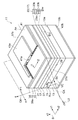
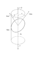
- FIG. 1 is a drawing schematically showing a group III nitride semiconductor laser according to the present embodiment.
- FIG. 2 is a drawing showing the structure of a light emitting diode in Example 1.
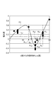
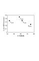
- FIG. 3 is a diagram showing the relationship between the off angle and the degree of polarization.
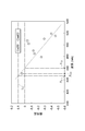
- FIG. 4 is a drawing showing the relationship between the peak emission wavelength and the degree of polarization in the LED mode at a typical inclination angle A OFF (inclination of 58 degrees in the a-axis direction and 62 degrees in the m-axis direction).
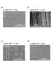
- FIG. 5 is a drawing showing a cathodoluminescence image of an LED structure.
- FIG. 6 is a diagram for explaining the Schmid factor.
- FIG. 1 is a drawing schematically showing a group III nitride semiconductor laser according to the present embodiment.
- FIG. 2 is a drawing showing the structure of a light emitting diode in Example 1.
- FIG. 3 is a diagram showing the relationship between the off angle and
- FIG. 7 is a diagram showing the relationship between the off angle and the Schmid factor.
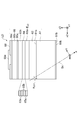
- FIG. 8 is a drawing showing structures of an epitaxial wafer and a semiconductor laser in Example 2.
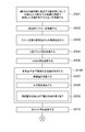
- FIG. 9 is a drawing showing main steps in a method for producing an epitaxial wafer and a semiconductor laser in Example 2.
- FIG. 10 is a drawing showing main steps in a method for producing an epitaxial wafer and a semiconductor laser in Example 2.
- Figure 11 is a view showing the characteristics of the semiconductor laser D M and D C.
- FIG. 1 is a drawing schematically showing a group III nitride semiconductor laser according to the present embodiment.
- FIG. 1 shows an orthogonal coordinate system S having an X1 axis, an X2 axis, and an X3 axis, and a crystal coordinate system CR for indicating a-axis, m-axis, and c-axis orientations.
- the surface opposite to the (0001) plane of the gallium nitride based semiconductor is indicated by the notation (000-1) plane.
- the group III nitride semiconductor laser 11 includes a semiconductor substrate 13, a first cladding layer 15, an active layer 17, and a second cladding layer 19.
- the semiconductor substrate 13 has a main surface 13a and a back surface 13b.
- the semiconductor substrate 13 is made of a hexagonal group III nitride semiconductor, and the group III nitride semiconductor is, for example, GaN.
- the main surface 13a of the semiconductor substrate 13 is in any one of the a-axis direction and the m-axis direction of the group III nitride semiconductor with respect to a reference plane orthogonal to the reference axis Cx in the c-axis direction of the group III nitride semiconductor.
- the first cladding layer 15 is provided on the main surface 13a of the semiconductor substrate 13 and is made of a first conductivity type gallium nitride semiconductor.
- the gallium nitride semiconductor of the first cladding layer 15 is made of, for example, GaN, AlGaN, InAlGaN, or the like.
- the light guiding direction of the active layer 17 is the other of the a-axis direction and the m-axis direction, and the axis Ax indicates the waveguide direction in FIG.
- the guided light becomes laser light L0 emitted from the end face.
- the second cladding layer 19 is provided on the main surface 13a of the semiconductor substrate 13 and is made of a second conductivity type gallium nitride based semiconductor.
- the gallium nitride semiconductor of the second cladding layer 19 is made of, for example, GaN, AlGaN, InAlGaN, or the like.
- the active layer 17 is provided between the first cladding layer 15 and the second cladding layer 19.
- the active layer 17 has a multiple quantum well structure 22.
- the multiple quantum well structure 22 includes well layers 23a and barrier layers 23b that are alternately arranged in the X3 axis direction.
- the well layers 23a are made of InGaN
- the barrier layers 23b are made of GaN or InGaN.
- the group III nitride semiconductor laser 11 has a gain guide type having a waveguide direction (m-axis direction in FIG. 1) in the X1-axis direction.
- the n-type gallium nitride semiconductor region, the active layer, and the p-type gallium nitride semiconductor region are arranged on the semiconductor substrate 13 in the X3 axis direction.
- the degree of polarization P in the LED mode of the group III nitride semiconductor laser is ⁇ 1 or more due to at least one of the band gap energy difference between the well layer 23 a and the barrier layer 23 b and the thickness D W of the well layer 23. It is provided to be 0.1 or less.
- the light in the LED mode of the group III nitride semiconductor laser is light emitted from the active layer before the semiconductor laser reaches the laser oscillation.
- the group III nitride semiconductor laser 11 light emission using the c-plane exhibits random polarization, but optical anisotropy appears in light emission on a surface inclined from the c-plane, and the above-described 50 degrees to 70 degrees.
- the degree of polarization P of light in the LED mode of the semiconductor laser 11 can be reduced to a value close to zero, or can be a negative value.
- the polarization component of the light that matches the TE mode of the semiconductor laser 11 can be increased, and the threshold value of the semiconductor laser 11 is reduced.
- the degree of polarization in the LED mode can be reduced and finally set to a negative value.
- the degree of polarization increases and approaches “1” in a multiple quantum well structure having a strong compressive strain.
- the degree of polarization P in the above range (-1 or more and 0.1 or less) according to the present embodiment is provided by the action of quantum confinement rather than the action of compressive strain.
- the band gap energy difference between the well layer and the barrier layer is preferably increased, and the thickness of the well layer is preferably decreased. Increasing the In composition of the InGaN well layer to obtain long-wavelength emission makes it possible to enhance quantum confinement.
- the oscillation wavelength of the multiple quantum well structure 22 is 450 nm or more. Also, the oscillation wavelength can be 550 nm or less.
- the degree of polarization P shows wavelength dependence, and within this range, the degree of polarization P can be realized in the range of ⁇ 1 ⁇ P ⁇ 0.1.
- the thickness D W of the well layer 23a can be 2 nm or more. Also, the thickness D W can be 10 nm or less.
- a narrow well width facilitates providing a near zero or negative degree of polarization.
- the degree of polarization can be realized in the range of ⁇ 1 ⁇ P ⁇ 0.1 by using a well layer having a thickness of 2 nm to 10 nm.
- the group III nitride semiconductor laser 11 can further include an InGaN layer 27.
- the InGaN layer 27 is provided between the first cladding layer 15 and the active layer 17.
- the InGaN layer 27 functions as a buffer layer for adjusting the stress on the active layer 17.
- the InGaN layer 27 is in contact with the main surface of the first cladding layer 15, and the lattice constant of the first cladding layer 15 is different from the lattice constant of the InGaN layer 27.
- the InGaN layer 27 is in contact with the active layer 17, and the lattice constant of the well layer 23 a of the active layer 17 is different from the lattice constant of the InGaN layer 27.
- misfit dislocation there is a misfit dislocation at the interface 29 between the first cladding layer 15 and the InGaN layer 27.
- the InGaN layer 27 relaxes by introducing misfit dislocations, the anisotropy of strain in the active layer 17 changes. It is considered that the degree of polarization P in the range of ⁇ 1 ⁇ P ⁇ 0.1 can be realized by this change in distortion.
- misfit dislocations are introduced by the c-plane of the InGaN layer acting as a slip plane. This misfit dislocation is introduced by using a semiconductor substrate. Since a certain degree of dislocation density is required to change the strain anisotropy, the density of misfit dislocations can be 5 ⁇ 10 3 cm ⁇ 1 or more. Moreover, since a dislocation density that is too high can deteriorate crystal quality, the density of misfit dislocations can be 1 ⁇ 10 5 cm ⁇ 1 or less.
- Indium composition X of the InGaN (In X Ga 1-X N) layer 27 may be 0.01 or more. In order to introduce misfit dislocations, a certain amount of In composition is required. The indium composition X can be 0.1 or less. An In composition that is too high may degrade the crystal quality of the active layer 17.
- the thickness D 27 of the InGaN layer 27 is 20nm or more. In order to introduce misfit dislocations, a certain film thickness is required. This thickness D 27 can be 150 nm or less. A film thickness D that is too thick may degrade the crystal quality of the active layer 17.
- the group III nitride semiconductor laser 11 can further include a light guide layer 31.
- the light guide layer 31 is provided between the second cladding layer 19 and the active layer 17.
- the light guide layer 31 is made of InGaN.
- the InGaN layer 27 acts as a lower light guide layer.
- These light guide layers 27 and 31 adjust the beam pattern of the laser, and the light guide layer 27 enables the introduction of misfit dislocations.
- the In composition of the light guide layer 31 can be, for example, 0.01 or more and 0.1 or less.
- the light guide layer 27 can be made of undoped InGaN, and the light guide layer 31 can be made of undoped InGaN.
- the group III nitride semiconductor laser 11 further includes an electron block layer 33 provided between the second cladding layer 19 and the active layer 17.
- the band gap of the electron block layer 33 is larger than that of the light guide layer 31 and larger than that of the second cladding layer 19.
- the electron block layer 33 is made of, for example, AlGaN.
- the group III nitride semiconductor laser 11 further includes a contact layer 35 provided on the second cladding layer 19 when necessary.
- the contact layer 35 has a dopant concentration higher than that of the second cladding layer 19.
- the contact layer 35 can be made of, for example, p-type GaN.
- the group III nitride semiconductor laser 11 can further include a pair of end faces 37a and 37b formed by cleavage planes.
- a cleavage plane in the m plane is possible.
- End faces 37a and 37b of group III nitride semiconductor laser 11 are m-plane cleavage planes.
- a resonator of the group III nitride semiconductor laser 11 can be configured using the m-plane cleavage plane.
- a cleavage plane in the a-plane is possible.
- End faces 37a and 37b of group III nitride semiconductor laser 11 are a-plane cleavage planes.
- a resonator of the group III nitride semiconductor laser 11 can be configured using the a-plane cleavage plane.
- the angle formed between the end faces 37a and 37b and the axis Ax indicating the waveguide direction can be in the range of ⁇ 1 degree or more and +1 degree or less.
- the main surface 13a of the semiconductor substrate 13 can be inclined in the a-axis direction, for example, when it is one of the (11-22) plane (off-angle 58 degrees a-axis direction) and the (11-2-2) plane. It is. Further, when the main surface 13a of the semiconductor substrate 13 is one of the (10-11) plane (off-angle 62 degrees m-axis direction) and the (10-1-1) plane, it can be inclined in the m-axis direction. It is.
- the group III nitride semiconductor laser further includes a protective film 41 covering the surface of the p-type gallium nitride semiconductor region 39a.
- the protective film 41 is provided with a contact window 41a extending in the waveguide direction.
- the electrode (for example, anode) 43a is in contact with the gallium nitride semiconductor region 39a through the contact window 41a.
- the electrode (for example, cathode) 43b makes contact with the back surface 13b of the semiconductor substrate 13b.
- a power source is connected between the anode and the cathode, a current flows from the anode to the cathode through the conductive semiconductor substrate.
- the semiconductor substrate 13 can be made of, for example, conductive GaN. GaN makes it possible to impart conductivity to the substrate and to provide good crystal quality epitaxial film growth. Moreover, a GaN wafer with an off angle can be produced.
- Example 1 Semipolar GaN wafers with various off angles were prepared.
- the angle (off angle) formed between the c-plane and the wafer main surface was, for example, 43 degrees in the m-axis direction, 58 degrees in the a-axis direction, 62 degrees in the m-axis direction, and 75 degrees in the m-axis method.
- a light emitting diode (LED) structure shown in FIG. 2 was fabricated on a GaN wafer.
- Epitaxial growth is performed by metal organic vapor phase epitaxy, and as raw materials for epitaxial growth, trimethyl gallium (TMG), trimethyl indium (TMI), trimethyl aluminum (TMA), ammonia (NH 3 ), silane (SiH 4 ), Biscyclopentadienyl magnesium (Cp 2 Mg) is used. The following steps are performed to manufacture the epitaxial wafer shown in FIG.
- Epitaxial growth was performed on the GaN wafer under the following conditions.
- the maximum value of the distance between two points on the edge of the GaN wafer is, for example, 45 mm or more.
- a GaN wafer was placed on a susceptor of a growth furnace in order to perform a pretreatment process.
- heat treatment was performed at a temperature of 1050 degrees Celsius while supplying NH 3 and H 2 to the growth furnace.
- the heat treatment time was 10 minutes, for example.
- the substrate temperature was changed to a temperature of 1150 degrees Celsius, for example.
- TMG, NH 3 , and SiH 4 were supplied to the growth reactor at a substrate temperature of 1150 degrees Celsius to grow a Si-doped GaN layer.
- the thickness of the GaN layer is 2 micrometers, for example.
- the following semiconductor layers were grown using a substrate temperature in the range of 650 degrees Celsius or more and 880 degrees Celsius or less in order to adjust the indium composition according to the off angle.
- TMG, TMI, NH 3 and SiH 4 were supplied to the growth reactor to grow a Si-doped InGaN layer.
- the thickness of the InGaN layer is, for example, 100 nm.
- the In composition of the InGaN layer is, for example, 0.04.
- a step of growing the active layer was performed.
- TMG and NH 3 were supplied to the growth reactor at the growth temperature (T B ) of the barrier layer to grow an undoped GaN barrier layer.
- the thickness of this GaN layer is 15 nm.
- the growth was interrupted after the growth of the GaN barrier layer, and the substrate temperature was changed from the growth temperature (T B ) to the growth temperature (T W ) of the well layer.
- TMG, TMI, and NH 3 were supplied to the growth reactor to grow an undoped InGaN well layer.
- the thickness of the InGaN well layer was 3 nm.
- the In composition X of this In X Ga 1-X N was, for example, 0.2.
- the supply of TMI was stopped.
- the substrate temperature was changed from the growth temperature (T W ) to the growth temperature (T B ) while supplying NH 3 to the growth reactor.
- a barrier layer growth step was performed to grow an undoped GaN barrier layer.
- the thickness of the GaN barrier layer is 15 nm.
- the InGaN well layer and the GaN barrier layer were formed by repeating the growth of the well layer, the temperature change, and the growth of the barrier layer.
- a p-type GaN-based semiconductor region is grown on the active layer.
- the supply of TMG was stopped and the substrate temperature was raised to 1000 degrees Celsius.
- TMG, TMA, NH 3 and Cp 2 Mg were supplied to the growth reactor to grow a p-type Al 0.18 Ga 0.82 N electron blocking layer. This electron block layer was 20 nm, for example.
- the supply of TMA was stopped and a p-type GaN contact layer was grown.
- the p-type GaN contact layer was 50 nm, for example.
- the temperature of the growth furnace was lowered to room temperature to produce an epitaxial wafer E LED .
- an electrode is formed on the epitaxial wafer E LED .
- a p-side electrode transparent electrode Ni / Au
- a p-pad electrode Ti / Au
- An n-side electrode Ti / Al
- electrode annealing eg, 550 degrees Celsius for 1 minute
- FIG. 2 is a view showing a structure of a light emitting diode structure LED and an epitaxial wafer E LED for the same.
- the light emitting diode structure LED and the epitaxial wafer E LED include an n-type GaN semiconductor layer 52, an n-type InGaN layer 53, an active layer 54, a p-type electron block layer 55, and a p-type grown in this order on the main surface 51a of the GaN wafer 51.
- a contact layer 56 is included.
- the active layer 54 includes a barrier layer 54a and a well layer 54b.
- An anode 57a is formed on the contact layer 56 of the epitaxial wafer E LED
- a cathode 57b is formed on the back surface 51b of the GaN wafer.
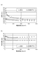
- FIG. 3 is a diagram showing the relationship between the off angle and the degree of polarization.
- m-axis direction 43 degrees (arrow A 43 )
- a-axis direction 58 degrees (arrow A 58 )
- m-axis direction 62 degrees (arrow A 62 )
- m-axis method 75 degrees (arrow A 75 ). It is shown.
- the polarization degree characteristic line P0 indicates zero polarization at angles A D0 and A U0 . From FIG.
- the angle A D0 is about 50 degrees
- the angle A U0 is about 68 degrees
- the polarization degree characteristic line P0 shows a degree of polarization of 0.1 at angles A D and A U.
- the angle AD is about 49 degrees
- the angle AU is about 73 degrees.
- the polarization degree characteristic line P0 once increases in the positive polarization degree region as the tilt angle A OFF from the c-plane increases. However, when the inclination angle exceeds 30 degrees, the polarization degree characteristic line P0 decreases as the inclination angle A OFF increases, and becomes a degree of polarization of 0.1 or less per angle AD , and further, the angle AD0. Negative value per hit.
- FIG. 4 is a drawing showing the relationship between the peak emission wavelength and the degree of polarization in the LED mode at typical inclination angles A OFF of 58 degrees (a-axis direction inclination) and 62 degrees (m-axis direction inclination).
- the degree of polarization is 0.1 at a wavelength ⁇ L in the vicinity of a wavelength of 450 nm. Further, the polarization degree becomes zero at a wavelength ⁇ 0 in the vicinity of 460 nm.
- the wavelength ⁇ S1 is 450 nm.
- the polarization degree P shows wavelength dependency.
- the degree of polarization P can be realized in the range of ⁇ 1 ⁇ P ⁇ 0.1 in the peak oscillation wavelength range of 450 nm to 550 nm.
- the peak oscillation wavelength of the multiple quantum well structure can be 460 nm or more and 550 nm or less.
- a low threshold value can be realized.
- the polarization degree P is a negative value.
- FIG. 5 is a drawing showing a cathode luminescence (CL) image of an LED structure. 5 (a) to 5 (d), respectively, the m-axis direction is 43 degrees off (polarization degree: 0.52), the a-axis direction is 58 degrees off (polarization degree: -0.29), and the m-axis direction 62.
- the acceleration voltage in the measurement of the CL image was set so that the accelerated electrons could reach the InGaN layer.
- a dark line entering the direction perpendicular to the off direction was observed. Judging from the direction of the dark line, it is considered that the c-plane is a slip surface and misfit dislocations are introduced.
- a dislocation half loop spreads on a plane inclined with respect to the semipolar plane (slip plane), so that the slip plane and the interface (in the above LED structure, the InGaN layer and the n-type GaN layer Misfit dislocations are introduced at positions where the (interfacial) intersects.
- the degree of polarization P decreases.
- the behavior of the polarization degree P can be explained as follows by the increase in the In composition of the well layer.
- a well layer with a large In composition is considered to have a strong quantum confinement effect.
- the result of FIG. 5 can also be explained by an increase in the In composition of the well layer. Since a well layer having a large In composition gives a large stress to the interface between the InGaN layer and the n-type GaN layer, misfit dislocations are likely to occur at this interface.
- the Schmid factor of the c-plane is estimated.
- This Schmitt factor represents the extent to which slip occurs on the c-plane.
- the Schmid factor will be described with reference to FIG. In FIG. 6, a part of the InGaN layer is shown as a cylindrical object.
- the c-plane slip surface S slip is inclined with respect to the axis Ax in the direction indicated by the normal vector N slip .
- the c-plane slip plane S slip slip slips in the direction (c-axis direction) indicated by the slip vector D slip .
- FIG. 7 is a diagram showing the relationship between the off angle and the Schmid factor.
- the size of the Schmid factor is in the following order: F Sa58 > F Sm62 > F Sm43 > F Sm75 (2)
- the order represented by Equation (2) qualitatively supports the relationship between the occurrence of dark lines and the off angle in the CL image.
- misfit dislocations are observed in the LED structure on the GaN substrate of 58 degrees in the a-axis direction and the LED structure on the GaN substrate of 62 degrees in the m-axis direction.
- the boundary of occurrence of misfit dislocation is 50 degrees or less and an angle in the vicinity of 50 degrees, and 70 degrees or more and an angle in the vicinity of 70 degrees.
- Example 2 In Example 1, the relationship between the degree of polarization and the angle was found by observing light emission from the LED structure.
- a semiconductor laser structure was fabricated on a GaN wafer inclined 58 degrees in the a-axis direction. Epitaxial growth is performed by metal organic vapor phase epitaxy, and as raw materials for epitaxial growth, trimethyl gallium (TMG), trimethyl indium (TMI), trimethyl aluminum (TMA), ammonia (NH 3 ), silane (SiH 4 ), Biscyclopentadienyl magnesium (Cp 2 Mg) is used. The manufacturing process of the epitaxial wafer and the semiconductor laser shown in FIG. 8 will be described with reference to FIGS.
- step S101 a semipolar GaN wafer having an inclination angle in the range of 50 degrees to 70 degrees was prepared.
- a GaN wafer 61 inclined 58 degrees in the a-axis direction was prepared.
- Epitaxial growth was performed on the GaN wafer 61 under the following conditions.
- step S102 the GaN wafer 61 was placed on the susceptor of the growth reactor.
- step S103 heat treatment was performed at a temperature of 1050 degrees Celsius while supplying NH 3 and H 2 to the growth furnace for pretreatment. The heat treatment time was 10 minutes, for example.
- step S104 the substrate temperature was changed to a temperature of 1150 degrees Celsius, for example, in order to grow an n-type semiconductor.
- TMG, TMA, NH 3 , and SiH 4 were supplied to the growth reactor at a substrate temperature of 1150 degrees Celsius, and the Si-doped AlGaN layer 62 was grown on the main surface 61 a of the GaN wafer 61.
- the thickness of the AlGaN layer 62 is, for example, 2 micrometers.
- the Al composition of the AlGaN layer 62 is, for example, 0.04.
- TMG, TMI, and NH 3 were supplied to the growth reactor at a substrate temperature of 840 degrees Celsius to grow the InGaN layer 63a on the AlGaN layer 62.
- the thickness of the InGaN layer 63a is, for example, 100 nm, and the In composition is, for example, 0.04.
- This InGaN layer 63a also functions as a light guide layer.
- Step S106 for growing the active layer 64 was performed.
- TMG and NH 3 were supplied to the growth reactor at a growth temperature (T B ) of 860 degrees Celsius to grow the undoped GaN barrier layer 65a.
- the thickness of the GaN layer 65a is, for example, 15 nm.
- T W growth temperature
- T W growth temperature
- the In composition X of this In X Ga 1 -X N was, for example, 0.18.
- the In composition X can be, for example, in the range of 0.10 to 0.40.
- the substrate temperature was changed from the growth temperature (T W ) to the growth temperature (T B ).
- the barrier layer growth step S107 was performed to grow the undoped GaN barrier layer 65a.
- the thickness of the GaN barrier layer 65a is, for example, 15 nm.
- the repeating step S109 the growth of the well layer 65b, the temperature change, and the growth of the barrier layer 65a were repeated to form a multiple quantum well structure including the alternately arranged GaN barrier layers 65a and InGaN well layers 65b.
- TMG, TMI, and NH 3 were supplied to the growth reactor at a substrate temperature of 840 degrees Celsius to grow the InGaN layer 63b on the active layer 64.
- the thickness of the InGaN layer is, for example, 100 nm, and the In composition is, for example, 0.04.
- a p-type GaN-based semiconductor region 66 is grown on the InGaN layer 63b.
- the supply of TMG was stopped and the substrate temperature was raised to 1000 degrees Celsius.
- TMG, TMA, NH 3 , and Cp 2 Mg were supplied to the growth reactor, and the p-type AlGaN electron block layer 66a was grown on the InGaN light guide layer 63b.
- This electron block layer 66a was 20 nm, for example.
- the Al composition of the electron block layer 66a was 0.18, for example.
- TMG, TMA, NH 3 , and Cp 2 Mg were supplied to the growth reactor, and the p-type AlGaN cladding layer 66b was grown on the electron block layer 66a.
- the p-type cladding layer 66b is 400 nm, for example.
- the Al composition of the p-type cladding layer 66b was, for example, 0.04.
- the supply of TMA was stopped, and a p-type GaN contact layer 66c was grown on the p-type cladding layer 66b.
- the p-type GaN contact layer 66c is, for example, 50 nm.
- the temperature was lowered in the growth furnace to room temperature to prepare an epitaxial wafer E LD.
- the electrode forming step S112 on the epitaxial wafer E LD, after forming the insulating film 68 having a contact window to form a p-side electrode 69a and the n-side electrode 69b on the epitaxial wafer E LD.
- a p-side transparent electrode (Ni / Au) is formed on the p-type GaN contact layer 66c.
- an anode pad electrode (Ti / Au) is formed.
- the insulating film is, for example, a silicon oxide film.
- the contact window has, for example, a stripe shape with a width of 10 ⁇ m.
- a cathode electrode (Ti / Al) is formed on the back surface 61 b of the GaN wafer 61. This is followed by electrode annealing (eg, 550 degrees Celsius for 1 minute). Through this process, a substrate product of the semiconductor light emitting device was obtained.
- the substrate product was cleaved at predetermined intervals to create a laser resonator.
- the laser resonator includes a pair of m-plane cleavage planes.
- FIG. 11 is a view showing the characteristics of the semiconductor laser D M and D C. Referring to FIG. 11A, the relationship between the injection current density and the peak wavelength of the emission spectrum in the LED mode is shown. FIG. 11B shows the relationship between the injection current density and the half-value width of the emission spectrum in the LED mode.
- the semiconductor laser D M is fabricated on a semipolar plane (a plane inclined by 58 degrees in the a-axis direction), the blue shift of the semiconductor laser D M is smaller than that of the semiconductor laser D C. Further, the half width of the semiconductor laser D M is small in comparison with the semiconductor laser D C.
- the behavior of full width at half maximum is understood as follows. Since the semiconductor laser D C represents a large piezoelectric effect, a difference in carrier density for each well layer of the active layer is caused depending on the amount of current injected into the active layer. Due to the difference in carrier density, a difference occurs in the degree of piezo screening of each well layer. For this reason, a half value width becomes large in the emission spectrum of LED mode.
- the piezoelectric polarization of the semiconductor laser D M is small compared to the semiconductor laser D C, varying degrees of piezoelectric screening in the well layers is small.
- the well layer of the semiconductor laser D M non-uniformity of In composition is smaller than that of the semiconductor laser D C.
- the uniformity of the In composition also contributes to the reduction of the half width in the emission spectrum of the LED mode.
- Polarization degree was measured by injecting a current 5mA in the semiconductor laser D M was +0.02. This degree of polarization is small compared to the previous reported examples.
- the laser oscillation occurs in the semiconductor laser D M at 850mA current.
- the semiconductor laser D C laser oscillation occurred at a current of 900 mA.
- a semiconductor laser having a very small degree of polarization (0.1 or less-1 or more) was obtained. It is considered that a threshold value lower than that of the comparative example was obtained by using an end face mirror by cleaving the m plane.
- SYMBOLS 11 Group III nitride semiconductor laser, 13 ... Semiconductor substrate, 15 ... 1st clad layer, 17 ... Active layer, 19 ... 2nd clad layer, 13a ... Semiconductor substrate main surface, 13b ... Semiconductor substrate back surface, 22 ... Multiple quantum well structure, 23a ... well layer, 23b ... barrier layer, P ... degree of polarization, 27 ... InGaN layer, 29 ... interface, 31 ... light guide layer, 33 ... electron blocking layer, 35 ... contact layer, 37a, 37b ... End face, 39a ... p-type gallium nitride semiconductor region, 41a ... contact window, 43a, 43b ...
Landscapes
- Physics & Mathematics (AREA)
- Optics & Photonics (AREA)
- Chemical & Material Sciences (AREA)
- Engineering & Computer Science (AREA)
- Nanotechnology (AREA)
- Condensed Matter Physics & Semiconductors (AREA)
- General Physics & Mathematics (AREA)
- Electromagnetism (AREA)
- Life Sciences & Earth Sciences (AREA)
- Biophysics (AREA)
- Crystallography & Structural Chemistry (AREA)
- Semiconductor Lasers (AREA)
Priority Applications (4)
| Application Number | Priority Date | Filing Date | Title |
|---|---|---|---|
| KR1020117020627A KR101269315B1 (ko) | 2009-02-17 | 2009-12-25 | Ⅲ족 질화물 반도체 레이저 및 ⅲ족 질화물 반도체 레이저를 제작하는 방법 |
| EP09840443A EP2400604A1 (en) | 2009-02-17 | 2009-12-25 | Iii nitride semiconductor laser and method for manufacturing iii nitride semiconductor laser |
| CN2009801569816A CN102318152B (zh) | 2009-02-17 | 2009-12-25 | Ⅲ族氮化物半导体激光器及ⅲ族氮化物半导体激光器的制作方法 |
| US13/211,858 US8548021B2 (en) | 2009-02-17 | 2011-08-17 | III-nitride semiconductor laser, and method for fabricating III-nitride semiconductor laser |
Applications Claiming Priority (2)
| Application Number | Priority Date | Filing Date | Title |
|---|---|---|---|
| JP2009034004A JP4775455B2 (ja) | 2009-02-17 | 2009-02-17 | Iii族窒化物半導体レーザ、及びiii族窒化物半導体レーザを作製する方法 |
| JP2009-034004 | 2009-02-17 |
Related Child Applications (1)
| Application Number | Title | Priority Date | Filing Date |
|---|---|---|---|
| US13/211,858 Continuation US8548021B2 (en) | 2009-02-17 | 2011-08-17 | III-nitride semiconductor laser, and method for fabricating III-nitride semiconductor laser |
Publications (1)
| Publication Number | Publication Date |
|---|---|
| WO2010095340A1 true WO2010095340A1 (ja) | 2010-08-26 |
Family
ID=42633632
Family Applications (1)
| Application Number | Title | Priority Date | Filing Date |
|---|---|---|---|
| PCT/JP2009/071661 Ceased WO2010095340A1 (ja) | 2009-02-17 | 2009-12-25 | Iii族窒化物半導体レーザ、及びiii族窒化物半導体レーザを作製する方法 |
Country Status (7)
| Country | Link |
|---|---|
| US (1) | US8548021B2 (enExample) |
| EP (1) | EP2400604A1 (enExample) |
| JP (1) | JP4775455B2 (enExample) |
| KR (1) | KR101269315B1 (enExample) |
| CN (1) | CN102318152B (enExample) |
| TW (1) | TW201034325A (enExample) |
| WO (1) | WO2010095340A1 (enExample) |
Cited By (3)
| Publication number | Priority date | Publication date | Assignee | Title |
|---|---|---|---|---|
| CN102227046A (zh) * | 2011-05-25 | 2011-10-26 | 北京化工大学 | 一种氮化镓基半导体激光器及其制作方法 |
| US20130100978A1 (en) * | 2011-10-24 | 2013-04-25 | The Regents Of The University Of California | Hole blocking layer for the prevention of hole overflow and non-radiative recombination at defects outside the active region |
| US11552452B2 (en) * | 2010-03-04 | 2023-01-10 | The Regents Of The University Of California | Semi-polar III-nitride optoelectronic devices on m-plane substrates with miscuts less than +/− 15 degrees in the c-direction |
Families Citing this family (11)
| Publication number | Priority date | Publication date | Assignee | Title |
|---|---|---|---|---|
| US7933303B2 (en) | 2009-06-17 | 2011-04-26 | Sumitomo Electric Industries, Ltd. | Group-III nitride semiconductor laser device, and method for fabricating group-III nitride semiconductor laser device |
| JP5206699B2 (ja) | 2010-01-18 | 2013-06-12 | 住友電気工業株式会社 | Iii族窒化物半導体レーザ素子、及びiii族窒化物半導体レーザ素子を作製する方法 |
| JP2011018784A (ja) * | 2009-07-09 | 2011-01-27 | Sony Corp | 半導体レーザ素子及びその駆動方法、並びに、半導体レーザ装置 |
| JP2011023537A (ja) * | 2009-07-15 | 2011-02-03 | Sumitomo Electric Ind Ltd | Iii族窒化物半導体素子、エピタキシャル基板、及びiii族窒化物半導体素子を作製する方法 |
| US8189639B2 (en) * | 2010-05-28 | 2012-05-29 | Corning Incorporated | GaN-based laser diodes with misfit dislocations displaced from the active region |
| JP5139555B2 (ja) * | 2011-04-22 | 2013-02-06 | 住友電気工業株式会社 | 窒化物半導体レーザ、及びエピタキシャル基板 |
| WO2015190171A1 (ja) * | 2014-06-10 | 2015-12-17 | ソニー株式会社 | 半導体光デバイス及びその製造方法並びに半導体光デバイス組立体 |
| KR102390624B1 (ko) | 2015-06-05 | 2022-04-26 | 오스텐도 테크놀로지스 인코포레이티드 | 다수의 활성층들로 선택적으로 캐리어를 주입한 발광 구조체 |
| US10396240B2 (en) * | 2015-10-08 | 2019-08-27 | Ostendo Technologies, Inc. | III-nitride semiconductor light emitting device having amber-to-red light emission (>600 nm) and a method for making same |
| DE112019003671T5 (de) | 2018-07-20 | 2021-04-08 | Sony Semiconductor Solutions Corporation | Halbleiterlichtemissionselement |
| JP7422496B2 (ja) * | 2019-06-21 | 2024-01-26 | 古河機械金属株式会社 | 構造体、光デバイス、光デバイスの製造方法、構造体の製造方法 |
Citations (4)
| Publication number | Priority date | Publication date | Assignee | Title |
|---|---|---|---|---|
| JPH0856046A (ja) * | 1994-08-12 | 1996-02-27 | Matsushita Electric Ind Co Ltd | 半導体レーザ |
| JP2008066717A (ja) * | 2006-08-11 | 2008-03-21 | Sanyo Electric Co Ltd | 半導体素子およびその製造方法 |
| JP2009016684A (ja) * | 2007-07-06 | 2009-01-22 | Nichia Corp | 半導体レーザ素子 |
| JP2009071127A (ja) * | 2007-09-14 | 2009-04-02 | Kyoto Univ | 窒化物半導体レーザ素子 |
Family Cites Families (5)
| Publication number | Priority date | Publication date | Assignee | Title |
|---|---|---|---|---|
| JP2005072368A (ja) | 2003-08-26 | 2005-03-17 | Sony Corp | 半導体発光素子、半導体レーザ素子、及び画像表示装置 |
| US7408199B2 (en) * | 2004-04-02 | 2008-08-05 | Nichia Corporation | Nitride semiconductor laser device and nitride semiconductor device |
| US7751455B2 (en) * | 2004-12-14 | 2010-07-06 | Palo Alto Research Center Incorporated | Blue and green laser diodes with gallium nitride or indium gallium nitride cladding laser structure |
| WO2008100504A1 (en) | 2007-02-12 | 2008-08-21 | The Regents Of The University Of California | Cleaved facet (ga,al,in)n edge-emitting laser diodes grown on semipolar {11-2n} bulk gallium nitride substrates |
| JP2009021346A (ja) | 2007-07-11 | 2009-01-29 | Rohm Co Ltd | 半導体発光素子 |
-
2009
- 2009-02-17 JP JP2009034004A patent/JP4775455B2/ja not_active Expired - Fee Related
- 2009-12-25 CN CN2009801569816A patent/CN102318152B/zh not_active Expired - Fee Related
- 2009-12-25 WO PCT/JP2009/071661 patent/WO2010095340A1/ja not_active Ceased
- 2009-12-25 KR KR1020117020627A patent/KR101269315B1/ko not_active Expired - Fee Related
- 2009-12-25 EP EP09840443A patent/EP2400604A1/en not_active Withdrawn
- 2009-12-31 TW TW098146573A patent/TW201034325A/zh unknown
-
2011
- 2011-08-17 US US13/211,858 patent/US8548021B2/en not_active Expired - Fee Related
Patent Citations (4)
| Publication number | Priority date | Publication date | Assignee | Title |
|---|---|---|---|---|
| JPH0856046A (ja) * | 1994-08-12 | 1996-02-27 | Matsushita Electric Ind Co Ltd | 半導体レーザ |
| JP2008066717A (ja) * | 2006-08-11 | 2008-03-21 | Sanyo Electric Co Ltd | 半導体素子およびその製造方法 |
| JP2009016684A (ja) * | 2007-07-06 | 2009-01-22 | Nichia Corp | 半導体レーザ素子 |
| JP2009071127A (ja) * | 2007-09-14 | 2009-04-02 | Kyoto Univ | 窒化物半導体レーザ素子 |
Non-Patent Citations (3)
| Title |
|---|
| APPLIED PHYSICS LETTERS, vol. 91, pages 251197 |
| JAPANESE JOURNAL OF APPLIED PHYSICS, vol. 46, no. 33, 2007, pages L789 - L791 |
| JAPANESE JOURNAL OF APPLIED PHYSICS, vol. 46, no. 9, 2007, pages L187 - L189 |
Cited By (3)
| Publication number | Priority date | Publication date | Assignee | Title |
|---|---|---|---|---|
| US11552452B2 (en) * | 2010-03-04 | 2023-01-10 | The Regents Of The University Of California | Semi-polar III-nitride optoelectronic devices on m-plane substrates with miscuts less than +/− 15 degrees in the c-direction |
| CN102227046A (zh) * | 2011-05-25 | 2011-10-26 | 北京化工大学 | 一种氮化镓基半导体激光器及其制作方法 |
| US20130100978A1 (en) * | 2011-10-24 | 2013-04-25 | The Regents Of The University Of California | Hole blocking layer for the prevention of hole overflow and non-radiative recombination at defects outside the active region |
Also Published As
| Publication number | Publication date |
|---|---|
| KR101269315B1 (ko) | 2013-05-29 |
| US8548021B2 (en) | 2013-10-01 |
| JP4775455B2 (ja) | 2011-09-21 |
| KR20110112472A (ko) | 2011-10-12 |
| JP2010192594A (ja) | 2010-09-02 |
| EP2400604A1 (en) | 2011-12-28 |
| TW201034325A (en) | 2010-09-16 |
| CN102318152A (zh) | 2012-01-11 |
| US20120008660A1 (en) | 2012-01-12 |
| CN102318152B (zh) | 2013-06-05 |
Similar Documents
| Publication | Publication Date | Title |
|---|---|---|
| JP4775455B2 (ja) | Iii族窒化物半導体レーザ、及びiii族窒化物半導体レーザを作製する方法 | |
| JP5003527B2 (ja) | Iii族窒化物発光素子、及びiii族窒化物系半導体発光素子を作製する方法 | |
| US8067257B2 (en) | Nitride based semiconductor optical device, epitaxial wafer for nitride based semiconductor optical device, and method of fabricating semiconductor light-emitting device | |
| KR101267702B1 (ko) | 질화갈륨계 반도체 발광 소자, 질화갈륨계 반도체 발광 소자를 제작하는 방법, 질화갈륨계 발광 다이오드, 에피택셜 웨이퍼 및 질화갈륨계 발광 다이오드를 제작하는 방법 | |
| US20110212560A1 (en) | Method for fabricating nitride semiconductor light emitting device and method for fabricating epitaxial wafer | |
| JP4924185B2 (ja) | 窒化物半導体発光素子 | |
| JP5139555B2 (ja) | 窒化物半導体レーザ、及びエピタキシャル基板 | |
| JP5699983B2 (ja) | 窒化ガリウム系半導体を作製する方法、iii族窒化物半導体デバイスを作製する方法、及びiii族窒化物半導体デバイス | |
| KR20100099066A (ko) | 질화갈륨계 반도체 광소자, 질화갈륨계 반도체 광소자를 제조하는 방법 및 에피택셜 웨이퍼 | |
| JP2013033930A (ja) | Iii族窒化物半導体素子、及び、iii族窒化物半導体素子の製造方法 | |
| JP5326787B2 (ja) | Iii族窒化物半導体レーザダイオード、及びiii族窒化物半導体レーザダイオードを作製する方法 | |
| US20120327967A1 (en) | Group iii nitride semiconductor laser device, epitaxial substrate, method of fabricating group iii nitride semiconductor laser device | |
| WO2013065381A1 (ja) | 窒化物半導体発光素子、及び、窒化物半導体発光素子の作製方法 | |
| JP5379216B2 (ja) | Iii族窒化物半導体レーザ | |
| JP2009224602A (ja) | 窒化物半導体レーザ、窒化物半導体レーザを作製する方法、及び窒化物半導体レーザのためのエピタキシャルウエハ | |
| JP2011188000A (ja) | Iii族窒化物半導体レーザ、及びiii族窒化物半導体レーザを作製する方法 | |
| JP2012231192A (ja) | 窒化ガリウム系半導体発光素子、窒化ガリウム系半導体発光素子を作製する方法、窒化ガリウム系発光ダイオード、エピタキシャルウエハ、及び窒化ガリウム系発光ダイオードを作製する方法 | |
| JP5351290B2 (ja) | 窒化物半導体レーザ、及びエピタキシャル基板 | |
| JP2009259864A (ja) | Iii族窒化物半導体レーザ | |
| WO2014088030A1 (ja) | 窒化物半導体発光素子、窒化物半導体発光素子を作製する方法 | |
| JP2010010300A (ja) | 窒化ガリウム系半導体発光素子及びエピタキシャルウエハ | |
| JP2012109624A (ja) | Iii族窒化物発光素子、及びiii族窒化物系半導体発光素子を作製する方法 |
Legal Events
| Date | Code | Title | Description |
|---|---|---|---|
| WWE | Wipo information: entry into national phase |
Ref document number: 200980156981.6 Country of ref document: CN |
|
| 121 | Ep: the epo has been informed by wipo that ep was designated in this application |
Ref document number: 09840443 Country of ref document: EP Kind code of ref document: A1 |
|
| NENP | Non-entry into the national phase |
Ref country code: DE |
|
| ENP | Entry into the national phase |
Ref document number: 20117020627 Country of ref document: KR Kind code of ref document: A |
|
| WWE | Wipo information: entry into national phase |
Ref document number: 2009840443 Country of ref document: EP |