EP2400604A1 - Iii nitride semiconductor laser and method for manufacturing iii nitride semiconductor laser - Google Patents
Iii nitride semiconductor laser and method for manufacturing iii nitride semiconductor laser Download PDFInfo
- Publication number
- EP2400604A1 EP2400604A1 EP09840443A EP09840443A EP2400604A1 EP 2400604 A1 EP2400604 A1 EP 2400604A1 EP 09840443 A EP09840443 A EP 09840443A EP 09840443 A EP09840443 A EP 09840443A EP 2400604 A1 EP2400604 A1 EP 2400604A1
- Authority
- EP
- European Patent Office
- Prior art keywords
- layer
- iii
- semiconductor laser
- nitride semiconductor
- axis
- Prior art date
- Legal status (The legal status is an assumption and is not a legal conclusion. Google has not performed a legal analysis and makes no representation as to the accuracy of the status listed.)
- Withdrawn
Links
- 239000004065 semiconductor Substances 0.000 title claims abstract description 226
- 238000000034 method Methods 0.000 title claims description 22
- 238000004519 manufacturing process Methods 0.000 title description 6
- 150000004767 nitrides Chemical class 0.000 title 2
- 230000010287 polarization Effects 0.000 claims abstract description 82
- 238000005253 cladding Methods 0.000 claims abstract description 64
- 239000000758 substrate Substances 0.000 claims abstract description 50
- 230000005684 electric field Effects 0.000 claims abstract description 12
- 229910002601 GaN Inorganic materials 0.000 claims description 75
- 230000004888 barrier function Effects 0.000 claims description 41
- JMASRVWKEDWRBT-UHFFFAOYSA-N Gallium nitride Chemical compound [Ga]#N JMASRVWKEDWRBT-UHFFFAOYSA-N 0.000 claims description 39
- 239000000203 mixture Substances 0.000 claims description 34
- 230000003287 optical effect Effects 0.000 claims description 33
- 229910052738 indium Inorganic materials 0.000 claims description 11
- APFVFJFRJDLVQX-UHFFFAOYSA-N indium atom Chemical compound [In] APFVFJFRJDLVQX-UHFFFAOYSA-N 0.000 claims description 11
- 235000012431 wafers Nutrition 0.000 description 24
- QGZKDVFQNNGYKY-UHFFFAOYSA-N Ammonia Chemical compound N QGZKDVFQNNGYKY-UHFFFAOYSA-N 0.000 description 21
- XCZXGTMEAKBVPV-UHFFFAOYSA-N trimethylgallium Chemical compound C[Ga](C)C XCZXGTMEAKBVPV-UHFFFAOYSA-N 0.000 description 18
- 229910000069 nitrogen hydride Inorganic materials 0.000 description 17
- 229910002704 AlGaN Inorganic materials 0.000 description 12
- 239000013078 crystal Substances 0.000 description 11
- JLTRXTDYQLMHGR-UHFFFAOYSA-N trimethylaluminium Chemical compound C[Al](C)C JLTRXTDYQLMHGR-UHFFFAOYSA-N 0.000 description 10
- IBEFSUTVZWZJEL-UHFFFAOYSA-N trimethylindium Chemical compound C[In](C)C IBEFSUTVZWZJEL-UHFFFAOYSA-N 0.000 description 10
- 230000008859 change Effects 0.000 description 9
- 238000005136 cathodoluminescence Methods 0.000 description 8
- BLRPTPMANUNPDV-UHFFFAOYSA-N Silane Chemical compound [SiH4] BLRPTPMANUNPDV-UHFFFAOYSA-N 0.000 description 7
- 230000009471 action Effects 0.000 description 6
- 238000007669 thermal treatment Methods 0.000 description 6
- 239000011777 magnesium Substances 0.000 description 5
- 230000009467 reduction Effects 0.000 description 5
- 238000003776 cleavage reaction Methods 0.000 description 4
- 238000000295 emission spectrum Methods 0.000 description 4
- 230000007017 scission Effects 0.000 description 4
- 230000007423 decrease Effects 0.000 description 3
- 230000000694 effects Effects 0.000 description 3
- 238000007781 pre-processing Methods 0.000 description 3
- 238000005086 pumping Methods 0.000 description 3
- USZGMDQWECZTIQ-UHFFFAOYSA-N [Mg](C1C=CC=C1)C1C=CC=C1 Chemical compound [Mg](C1C=CC=C1)C1C=CC=C1 USZGMDQWECZTIQ-UHFFFAOYSA-N 0.000 description 2
- 229910021529 ammonia Inorganic materials 0.000 description 2
- 230000015572 biosynthetic process Effects 0.000 description 2
- 230000003247 decreasing effect Effects 0.000 description 2
- 230000006866 deterioration Effects 0.000 description 2
- 238000002474 experimental method Methods 0.000 description 2
- 125000002524 organometallic group Chemical group 0.000 description 2
- 239000002994 raw material Substances 0.000 description 2
- 238000012216 screening Methods 0.000 description 2
- 229910000077 silane Inorganic materials 0.000 description 2
- VYPSYNLAJGMNEJ-UHFFFAOYSA-N silicon dioxide Inorganic materials O=[Si]=O VYPSYNLAJGMNEJ-UHFFFAOYSA-N 0.000 description 2
- 238000000927 vapour-phase epitaxy Methods 0.000 description 2
- 230000001133 acceleration Effects 0.000 description 1
- 230000000052 comparative effect Effects 0.000 description 1
- 230000000295 complement effect Effects 0.000 description 1
- 239000002019 doping agent Substances 0.000 description 1
- 238000005259 measurement Methods 0.000 description 1
- 238000012986 modification Methods 0.000 description 1
- 230000004048 modification Effects 0.000 description 1
- 238000011160 research Methods 0.000 description 1
- 229910052814 silicon oxide Inorganic materials 0.000 description 1
- 230000007704 transition Effects 0.000 description 1
Images


Classifications
-
- H—ELECTRICITY
- H01—ELECTRIC ELEMENTS
- H01S—DEVICES USING THE PROCESS OF LIGHT AMPLIFICATION BY STIMULATED EMISSION OF RADIATION [LASER] TO AMPLIFY OR GENERATE LIGHT; DEVICES USING STIMULATED EMISSION OF ELECTROMAGNETIC RADIATION IN WAVE RANGES OTHER THAN OPTICAL
- H01S5/00—Semiconductor lasers
- H01S5/30—Structure or shape of the active region; Materials used for the active region
- H01S5/34—Structure or shape of the active region; Materials used for the active region comprising quantum well or superlattice structures, e.g. single quantum well [SQW] lasers, multiple quantum well [MQW] lasers or graded index separate confinement heterostructure [GRINSCH] lasers
- H01S5/343—Structure or shape of the active region; Materials used for the active region comprising quantum well or superlattice structures, e.g. single quantum well [SQW] lasers, multiple quantum well [MQW] lasers or graded index separate confinement heterostructure [GRINSCH] lasers in AIIIBV compounds, e.g. AlGaAs-laser, InP-based laser
- H01S5/34333—Structure or shape of the active region; Materials used for the active region comprising quantum well or superlattice structures, e.g. single quantum well [SQW] lasers, multiple quantum well [MQW] lasers or graded index separate confinement heterostructure [GRINSCH] lasers in AIIIBV compounds, e.g. AlGaAs-laser, InP-based laser with a well layer based on Ga(In)N or Ga(In)P, e.g. blue laser
-
- B—PERFORMING OPERATIONS; TRANSPORTING
- B82—NANOTECHNOLOGY
- B82Y—SPECIFIC USES OR APPLICATIONS OF NANOSTRUCTURES; MEASUREMENT OR ANALYSIS OF NANOSTRUCTURES; MANUFACTURE OR TREATMENT OF NANOSTRUCTURES
- B82Y20/00—Nanooptics, e.g. quantum optics or photonic crystals
-
- H—ELECTRICITY
- H01—ELECTRIC ELEMENTS
- H01S—DEVICES USING THE PROCESS OF LIGHT AMPLIFICATION BY STIMULATED EMISSION OF RADIATION [LASER] TO AMPLIFY OR GENERATE LIGHT; DEVICES USING STIMULATED EMISSION OF ELECTROMAGNETIC RADIATION IN WAVE RANGES OTHER THAN OPTICAL
- H01S2304/00—Special growth methods for semiconductor lasers
- H01S2304/04—MOCVD or MOVPE
-
- H—ELECTRICITY
- H01—ELECTRIC ELEMENTS
- H01S—DEVICES USING THE PROCESS OF LIGHT AMPLIFICATION BY STIMULATED EMISSION OF RADIATION [LASER] TO AMPLIFY OR GENERATE LIGHT; DEVICES USING STIMULATED EMISSION OF ELECTROMAGNETIC RADIATION IN WAVE RANGES OTHER THAN OPTICAL
- H01S5/00—Semiconductor lasers
- H01S5/02—Structural details or components not essential to laser action
- H01S5/0201—Separation of the wafer into individual elements, e.g. by dicing, cleaving, etching or directly during growth
- H01S5/0202—Cleaving
-
- H—ELECTRICITY
- H01—ELECTRIC ELEMENTS
- H01S—DEVICES USING THE PROCESS OF LIGHT AMPLIFICATION BY STIMULATED EMISSION OF RADIATION [LASER] TO AMPLIFY OR GENERATE LIGHT; DEVICES USING STIMULATED EMISSION OF ELECTROMAGNETIC RADIATION IN WAVE RANGES OTHER THAN OPTICAL
- H01S5/00—Semiconductor lasers
- H01S5/20—Structure or shape of the semiconductor body to guide the optical wave ; Confining structures perpendicular to the optical axis, e.g. index or gain guiding, stripe geometry, broad area lasers, gain tailoring, transverse or lateral reflectors, special cladding structures, MQW barrier reflection layers
- H01S5/2004—Confining in the direction perpendicular to the layer structure
- H01S5/2009—Confining in the direction perpendicular to the layer structure by using electron barrier layers
-
- H—ELECTRICITY
- H01—ELECTRIC ELEMENTS
- H01S—DEVICES USING THE PROCESS OF LIGHT AMPLIFICATION BY STIMULATED EMISSION OF RADIATION [LASER] TO AMPLIFY OR GENERATE LIGHT; DEVICES USING STIMULATED EMISSION OF ELECTROMAGNETIC RADIATION IN WAVE RANGES OTHER THAN OPTICAL
- H01S5/00—Semiconductor lasers
- H01S5/30—Structure or shape of the active region; Materials used for the active region
- H01S5/32—Structure or shape of the active region; Materials used for the active region comprising PN junctions, e.g. hetero- or double- heterostructures
- H01S5/3202—Structure or shape of the active region; Materials used for the active region comprising PN junctions, e.g. hetero- or double- heterostructures grown on specifically orientated substrates, or using orientation dependent growth
- H01S5/320275—Structure or shape of the active region; Materials used for the active region comprising PN junctions, e.g. hetero- or double- heterostructures grown on specifically orientated substrates, or using orientation dependent growth semi-polar orientation
-
- H—ELECTRICITY
- H01—ELECTRIC ELEMENTS
- H01S—DEVICES USING THE PROCESS OF LIGHT AMPLIFICATION BY STIMULATED EMISSION OF RADIATION [LASER] TO AMPLIFY OR GENERATE LIGHT; DEVICES USING STIMULATED EMISSION OF ELECTROMAGNETIC RADIATION IN WAVE RANGES OTHER THAN OPTICAL
- H01S5/00—Semiconductor lasers
- H01S5/30—Structure or shape of the active region; Materials used for the active region
- H01S5/32—Structure or shape of the active region; Materials used for the active region comprising PN junctions, e.g. hetero- or double- heterostructures
- H01S5/3211—Structure or shape of the active region; Materials used for the active region comprising PN junctions, e.g. hetero- or double- heterostructures characterised by special cladding layers, e.g. details on band-discontinuities
-
- H—ELECTRICITY
- H01—ELECTRIC ELEMENTS
- H01S—DEVICES USING THE PROCESS OF LIGHT AMPLIFICATION BY STIMULATED EMISSION OF RADIATION [LASER] TO AMPLIFY OR GENERATE LIGHT; DEVICES USING STIMULATED EMISSION OF ELECTROMAGNETIC RADIATION IN WAVE RANGES OTHER THAN OPTICAL
- H01S5/00—Semiconductor lasers
- H01S5/30—Structure or shape of the active region; Materials used for the active region
- H01S5/34—Structure or shape of the active region; Materials used for the active region comprising quantum well or superlattice structures, e.g. single quantum well [SQW] lasers, multiple quantum well [MQW] lasers or graded index separate confinement heterostructure [GRINSCH] lasers
- H01S5/3403—Structure or shape of the active region; Materials used for the active region comprising quantum well or superlattice structures, e.g. single quantum well [SQW] lasers, multiple quantum well [MQW] lasers or graded index separate confinement heterostructure [GRINSCH] lasers having a strained layer structure in which the strain performs a special function, e.g. general strain effects, strain versus polarisation
- H01S5/3404—Structure or shape of the active region; Materials used for the active region comprising quantum well or superlattice structures, e.g. single quantum well [SQW] lasers, multiple quantum well [MQW] lasers or graded index separate confinement heterostructure [GRINSCH] lasers having a strained layer structure in which the strain performs a special function, e.g. general strain effects, strain versus polarisation influencing the polarisation
-
- H—ELECTRICITY
- H10—SEMICONDUCTOR DEVICES; ELECTRIC SOLID-STATE DEVICES NOT OTHERWISE PROVIDED FOR
- H10H—INORGANIC LIGHT-EMITTING SEMICONDUCTOR DEVICES HAVING POTENTIAL BARRIERS
- H10H20/00—Individual inorganic light-emitting semiconductor devices having potential barriers, e.g. light-emitting diodes [LED]
- H10H20/80—Constructional details
- H10H20/81—Bodies
- H10H20/817—Bodies characterised by the crystal structures or orientations, e.g. polycrystalline, amorphous or porous
-
- H—ELECTRICITY
- H10—SEMICONDUCTOR DEVICES; ELECTRIC SOLID-STATE DEVICES NOT OTHERWISE PROVIDED FOR
- H10H—INORGANIC LIGHT-EMITTING SEMICONDUCTOR DEVICES HAVING POTENTIAL BARRIERS
- H10H20/00—Individual inorganic light-emitting semiconductor devices having potential barriers, e.g. light-emitting diodes [LED]
- H10H20/80—Constructional details
- H10H20/81—Bodies
- H10H20/822—Materials of the light-emitting regions
- H10H20/824—Materials of the light-emitting regions comprising only Group III-V materials, e.g. GaP
- H10H20/825—Materials of the light-emitting regions comprising only Group III-V materials, e.g. GaP containing nitrogen, e.g. GaN
Definitions
- the present invention relates to a III-nitride semiconductor laser, and a method for fabricating the III-nitride semiconductor laser.
- Non-patent Document 1 shows an InGaN/GaN quantum well structure made on a GaN (11-22) substrate.
- An off angle of the GaN substrate is 58 degrees formed in the a-axis direction. Since a cavity structure cannot be formed with the above-described crystal facets, the quantum well structure is made to emit light by photo-pumping. Pumping light is guided in a direction along a plane defined by the c-axis and a-axis.
- This quantum well structure is disposed between GaN optical guide layers. An emission measured along the [-1-123] direction is generated with a lower energy and a lower threshold pumping power than an emission measured along the [1-100] direction.
- Non-patent Document 2 discloses laser diodes made on an m-plane.
- the laser diodes have the InGaN/GaN quantum well structure and the lasing wavelength thereof is 400 nm.
- This quantum well structure is disposed between GaN guide layers. Stripes parallel to the a- and c-axes show TE mode operation, and the c-axis stripe laser diode among such laser diodes exhibits the lower threshold current densities.
- Non-patent Document 3 shows theoretical calculation of polarization degree.
- a semiconductor laser is made on a c-plane GaN wafer. Fabrication of a semiconductor laser on a nonpolar plane (a-plane or m-plane) GaN wafer is under research because the piezoelectric field can be made substantially zero. Furthermore, attention is drawn to fabrication of a semiconductor laser on a semipolar GaN wafer, though influence of the piezoelectric field remains.
- the semiconductor lasers using the nonpolar and semipolar planes demonstrate optical anisotropy, and an orientation of cleaved edges is important for obtaining a low-threshold semiconductor laser.
- the semiconductor laser on the m-plane GaN substrate shows polarization in the a-axis direction as described in Non-patent Document 2, cleavage formed along the c-plane allows a component with a high transition probability to lase as TE mode.
- the laser structure in Non-patent Document 2 is applied to a semipolar plane inclined from a nonpolar plane, cleaved c-planes are inclined relative to the waveguide direction, thus failing to obtain a cavity.
- the polarization degrees in Non-patent Documents 1 and 2 are about 0.7 or higher.
- the polarization degree is associated with the threshold current. According to the inventors' knowledge, it is considered that the threshold current of the III-nitride semiconductor laser becomes low when the polarization degree is a negative value or a value close to zero.
- III-nitride semiconductor laser comprises:
- This III-nitride semiconductor laser is based on knowing that the emission of the optical device using the c-plane exhibits random polarization whereas the emission of the optical device using a plane inclined from the c-plane shows optical anisotropy and, with this inclined plane in the foregoing angular range of not less than 50 degrees and not more than 70 degrees, the polarization degree of light in the LED mode of the semiconductor laser can be made as small as a value close to zero, or a negative value.
- the polarization component of light directed to the TE mode of the semiconductor laser can be made larger than the others, and thus the threshold of the semiconductor laser can be lowered.
- a lasing wavelength of the multiple quantum well structure of the active layer can be not less than 450 nm and not more than 550 nm.
- the polarization degree has wavelength dependence and in the foregoing wavelength range, the polarization degree can fall within the range of-1 ⁇ P ⁇ 0.1.
- a thickness of the well layer can be not less than 2 nm and not more than 10 nm.
- the polarization degree can be realized in the range of -1 ⁇ P ⁇ 0.1, using the well layers in the thickness of not less than 2 nm and not more than 10 nm.
- a direction of the inclination is a direction of the a-axis.
- the III-nitride semiconductor laser can further comprise a pair of end faces comprising m-cleaved faces of the hexagonal III-nitride.
- a cavity of the III-nitride semiconductor laser can be constructed using the m-cleaved faces.
- the primary surface of the semiconductor substrate is, for example, either one of the (11-22) plane and the (11-2-2) plane.
- This III-nitride semiconductor laser allows for inclination in the direction from the c-axis to the a-axis.
- a direction of the inclination is a direction of the m-axis.
- the III-nitride semiconductor laser can further comprise a pair of end faces comprising a-cleaved faces of the hexagonal III-nitride.
- a cavity of the III-nitride semiconductor laser can be constructed using the a-cleaved faces.
- the primary surface of the semiconductor substrate is either one of the (10-11) plane and the (10-1-1) plane.
- This III-nitride semiconductor laser allows for inclination in the direction from to the m-axis.
- the semiconductor substrate comprises GaN.
- III-nitride semiconductor laser it is feasible to obtain an epitaxial film with excellent crystal quality, and it is also possible to fabricate an off-angled GaN wafer.
- the III-nitride semiconductor laser according to the present invention can further comprise an InGaN layer provided between the first cladding layer and the active layer.
- the InGaN layer acts as a buffer which can control stress on the active layer.
- an interface between the first cladding layer and the InGaN layer contains misfit dislocations.
- the relaxation of the InGaN layer through the misfit dislocations causes variation in anisotropy of strain.
- This variation in strain can be utilized for realizing the polarization degree in the range of -1 ⁇ P ⁇ 0.1.
- the misfit dislocations are considered to be introduced such that the c-plane of the InGaN layer acts as a slip plane.
- the misfit dislocations are introduced by use of the semiconductor substrate.
- an indium composition of the InGaN layer is not less than 0.01, the indium composition of the InGaN layer is not more than 0.1, the InGaN layer is in contact with a primary surface of the first cladding layer, and a lattice constant of the first cladding layer is different from that of the InGaN layer.
- a thickness of the InGaN layer is not less than 20 nm and the thickness of the InGaN layer is not more than 150 nm.
- the InGaN layer is a first optical guide layer
- the III-nitride semiconductor laser can further comprise a second optical guide layer provided between the second cladding layer and the active layer.
- the second optical guide layer comprises InGaN.
- the first and second optical guide layers comprising make it feasible to shape a beam pattern of the laser and to implement introduction of misfit dislocations.
- the polarization degree P has a negative value. This III-nitride semiconductor laser allows for realization of a low threshold.
- the angle of inclination is not less than 58 degrees and not more than 62 degrees.
- the polarization degree P has a negative value in this angular range.
- Another aspect of the present invention is a method for fabricating a III-nitride semiconductor laser.
- This method comprises the steps of: (a) preparing a semiconductor wafer, the semiconductor wafer comprising a hexagonal III-nitride semiconductor and having a primary surface, the primary surface being inclined at an angle of inclination in a range of not less than 50 degrees and not more than 70 degrees toward either one of an a-axis direction and an m-axis direction of the hexagonal III-nitride semiconductor with respect to a reference plane perpendicular to a reference axis, and the reference axis extending along the c-axis direction of the III-nitride semiconductor; (b) growing a first cladding layer of a first conductivity type gallium nitride-based semiconductor on the primary surface of the semiconductor wafer; (c) growing an active layer on the InGaN layer; and (d) growing a second cladding layer of a second conductivity type gallium nitride-based semiconductor on
- a waveguide direction in the active layer is directed along either one of the a-axis direction and the m-axis direction; in an orthogonal coordinate system having an X1 axis directed along the waveguide direction, an X2 axis perpendicular to the X1 axis and an X3 axis perpendicular to the X1 axis and the X2 axis, the n-type gallium nitride-based semiconductor region, the active layer and the p-type gallium nitride-based semiconductor region are arranged in a direction of the X3 axis;
- the active layer has a multiple quantum well structure comprising well layers and barrier layers, the well layers and barrier layers are arranged alternately in the direction of the X3 axis, the well layers comprises InGaN, and the barrier layers comprises GaN or InGaN;
- the multiple quantum well structure is provided such that at least either of a thickness of the well layers and a bandgap energy difference between the well layers and
- This method is based on knowing that the emission of the optical device using the c-plane exhibits random polarization whereas the emission of the optical device using the plane inclined from the c-plane shows optical anisotropy and, with the inclined plane in the foregoing angular range of not less than 50 degrees and not more than 70 degrees, the polarization degree of light in the LED mode of the semiconductor laser can be made as small as a value close to zero, or a negative value.
- the polarization component of light directed to the TE mode of the semiconductor laser can be made larger and thus the threshold of the semiconductor laser can be lowered.
- the method according to the present invention can further comprise the step of growing an InGaN layer on the first cladding layer, prior to the growth of the active layer.
- the InGaN layer acts as a buffer layer which can control stress on the active layer.
- an indium composition of the InGaN layer can be not less than 0.01 and the indium composition of the InGaN layer can be not more than 0.1.
- the InGaN layer is in contact with a primary surface of the first cladding layer, and a lattice constant of the first cladding layer is different from that of the InGaN layer.
- a thickness of the InGaN layer is not less than 20 nm and the thickness of the InGaN layer is not more than 150 nm.
- misfit dislocations are formed at an interface between the first cladding layer and the InGaN layer and a density of the misfit dislocations can be not less than 5 ⁇ 10 3 cm -1 and not more than 1 ⁇ 10 5 cm -1 .
- the present invention provides the III-nitride semiconductor laser realizing provision of the low threshold using the semipolar plane.
- the present invention also provides the method for fabricating the III-nitride semiconductor laser.
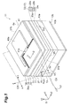
- Fig. 1 is a drawing schematically showing a III-nitride semiconductor laser according to the present embodiment. Shown in Fig. 1 is an orthogonal coordinate system S having X1 axis, X2 axis, and X3 axis, and a crystal coordinate system CR for showing the a-axis, m-axis, and c-axis directions. The description below will follow such a notation that, for example, a plane opposite to the (0001) plane of a GaN-based semiconductor is represented by (000-1) plane.
- the III-nitride semiconductor laser 11 has a semiconductor substrate 13, a first cladding layer 15, an active layer 17, and a second cladding layer 19.
- the semiconductor substrate 13 has a primary surface 13a and a back surface 13b.
- the semiconductor substrate 13 comprises a III-nitride semiconductor of a hexagonal system, and this III-nitride semiconductor is, for example, GaN or the like.
- the primary surface 13a of the semiconductor substrate 13 is inclined at an angle of inclination A OFF in the range of not less than 50 degrees and not more than 70 degrees toward respect to either one of the a-axis direction and the m-axis direction of the III-nitride semiconductor with respect to a reference plane perpendicular to the reference axis Cx that extends along the c-axis direction of the III-nitride semiconductor.
- This angle A OFF is equal to the complement of an angle between vector VC and vector VN in the present embodiment.
- Fig. 1 are a typical c-plane S C and the c-axis vector VC, and normal vector VN to the primary surface 13a is shown therein.
- the first cladding layer 15 is provided on the primary surface 13a of the semiconductor substrate 13, and comprises a first conductivity type GaN-based semiconductor.
- the GaN-based semiconductor of the first cladding layer 15 comprises, for example, GaN, AlGaN, InAlGaN, or the like.
- the waveguide direction of light in the active layer 17 is the other of the a-axis direction and the m-axis direction, and in Fig. 1 , the axis Ax indicates the waveguide direction.
- the guided light becomes a laser beam L0 emitted from an end face.
- the second cladding layer 19 is provided above the primary surface 13a of the semiconductor substrate 13, and comprises a second conductivity type GaN-based semiconductor.
- the GaN-based semiconductor of the second cladding layer 19 comprises, for example, GaN, AlGaN, InAlGaN, or the like.
- the active layer 17 is provided between the first cladding layer 15 and the second cladding layer 19.
- the active layer 17 has a multiple quantum well structure 22.
- the multiple quantum well structure 22 includes well layers 23a and barrier layers 23b arranged alternately in the direction of the X3 axis, the well layers 23a comprise InGaN, and the barrier layers 23b comprise GaN or InGaN.
- the III-nitride semiconductor laser 11 is categorized into a gain guiding type having the waveguide direction along the direction of the X1 axis (m-axis direction in Fig. 1 ).
- the n-type GaN-based semiconductor region, active layer, and p-type GaN-based semiconductor region are arranged in the direction of the X3 axis on the semiconductor substrate 13.
- the multiple quantum well structure is provided so that at least either of a bandgap energy difference between the well layers 23a and the barrier layers 23b and the thickness D W of the well layers 23 enables the polarization degree P in the LED mode of the III-nitride semiconductor laser to fall within the range of not less than -1 and not more than 0.1.
- Light in the LED mode of the III-nitride semiconductor laser is emitted from the active layer before the semiconductor laser reaches lasing.
- This III-nitride semiconductor laser 11 is based on knowing that the emission using the c-plane exhibits random polarization whereas the emission with the plane inclined from the c-plane exhibits optical anisotropy and, by use of the GaN inclined surface in the foregoing angular range of not less than 50 degrees and not more than 70 degrees (i.e., a semipolar plane), the polarization degree P of the light in the LED mode of the semiconductor laser 11 can be made as small as a value close to zero, or a negative value. At this time, it is feasible to make the polarization optical component of the TE mode large in the semiconductor laser 11 and thus to reduce the threshold of the semiconductor laser 11.
- the polarization degree in the LED mode can be reduced to a small value and eventually to a negative value.
- Concerning the polarization degree it increases toward "1" in multiple quantum well structures with strong compressive strain.
- the polarization degree P in the aforementioned range (not less than -1 and not more than 0.1) according to the present embodiment is considered to be provided by the action of quantum confinement, rather than by the action of compressive strain.
- An increase in the In composition of the InGaN well layers to obtain a long-wavelength emission enables enhancement of quantum confinement.
- the lasing wavelength of the multiple quantum well structure 22 is not less than 450 nm.
- the lasing wavelength can be not more than 550 nm.
- the polarization degree P shows wavelength dependence, and in the foregoing wavelength range, the polarization degree P can be realized in the range of -1 ⁇ P ⁇ 0.1.
- the thickness D W of the well layer 23a can be not less than 2 nm.
- the thickness D W can be not more than 10 nm.
- the narrow well width facilitates provision of the polarization degree close to zero or the negative polarization degree.
- the polarization degree can be realized in the range of -1 ⁇ P ⁇ 0.1, using the well layers in the thickness of not less than 2 nm and not more than 10 nm.
- the III-nitride semiconductor laser 11 can further comprise an InGaN layer 27.
- the InGaN layer 27 is provided between the first cladding layer 15 and the active layer 17.
- the InGaN layer 27 acts as a buffer layer for controlling stress on the active layer 17.
- the InGaN layer 27 is in contact with a primary surface of the first cladding layer 15, and the lattice constant of the first cladding layer 15 is different from that of the InGaN layer 27.
- the InGaN layer 27 is also in contact with the active layer 17, and the lattice constant of the well layers 23a of the active layer 17 is different from that of the InGaN layer 27.
- Misfit dislocations are provided at an interface 29 between the first cladding layer 15 and the InGaN layer 27.
- the InGaN layer 27 is relaxed by introduction of misfit dislocations, thereby causing variation in anisotropy of strain in the active layer 17. This variation in strain is considered to allow for realization of the polarization degree P in the range of -1 ⁇ P ⁇ 0.1.
- the misfit dislocations are considered to be introduced because the c-plane of the InGaN layer acts as a slip plane.
- the misfit dislocations are introduced by use of the semiconductor substrate. Since a certain level of dislocation density is needed for causing change in anisotropy of strain, the density of misfit dislocations can be not less than 5 ⁇ 10 3 cm -1 . Since there is a possibility that a too high dislocation density deteriorates the crystal quality, the density of misfit dislocations can be not more than 1 ⁇ 10 5 cm -1 .
- the indium composition X of the InGaN (In X Ga 1-X N) layer 27 can be not less than 0.01. A certain level of In composition is needed for the introduction of misfit dislocations.
- the indium composition X can be not more than 0.1. A too high In composition could lead to deterioration of crystal quality of the active layer 17.
- the thickness D 27 of the InGaN layer 27 can be not less than 20 nm. A certain level of film thickness is needed for the introduction of misfit dislocations. This thickness D 27 can be not more than 150 nm. A too large film thickness D could lead to deterioration of crystal quality of the active layer 17.
- the III-nitride semiconductor laser 11 can further comprise a optical guide layer 31.
- the optical guide layer 31 is provided between the second cladding layer 19 and the active layer 17.
- the optical guide layer 31 comprises InGaN.
- the InGaN layer 27 acts as a lower optical guide layer.
- These optical guide layers 27 and 31 define a beam pattern of the laser beam, and the optical guide layer 27 enables the introduction of misfit dislocations.
- An In composition of the optical guide layer 31 can be, for example, not less than 0.01 and not more than 0.1.
- the optical guide layer 27 can comprise undoped InGaN, and the optical guide layer 31 can comprise undoped InGaN.
- the III-nitride semiconductor laser 11 further includes an electron block layer 33 provided between the second cladding layer 19 and the active layer 17.
- the bandgap of the electron block layer 33 is larger than that of the optical guide layer 31 and also larger than that of the second cladding layer 19.
- the electron block layer 33 comprises, for example, AlGaN.
- the III-nitride semiconductor laser 11 further includes a contact layer 35 provided on the second cladding layer 19, if necessary.
- a dopant concentration of the contact layer 35 is larger than that of the second cladding layer 19.
- the contact layer 35 can comprise, for example, p-type GaN or the like.
- the III-nitride semiconductor laser 11 can further include a pair of end faces 37a, 37b composed of cleaved planes.
- the end faces 37a, 37b of the III-nitride semiconductor laser 11 use m-plane cleaved planes.
- a cavity of the III-nitride semiconductor laser 11 can be constructed using the m-plane cleaved planes.
- the end faces 37a, 37b of the III-nitride semiconductor laser 11 use a-plane cleaved planes.
- a cavity of the III-nitride semiconductor laser 11 can be constructed using the a-plane cleaved planes.
- An angle between the end faces 37a, 37b and the axis Ax indicating the waveguide direction can be in the range of not less than -1 degrees and not more than +1 degrees.
- the primary surface 13a of the semiconductor substrate 13 is, for example, either one of the (11-22) plane (off angle of 58 degrees defined in association with the a-axis direction) and the (11-2-2) plane, inclination with respect to the a-axis direction becomes possible.
- the primary surface 13a of the semiconductor substrate 13 is either one of the (10-11) plane (off angle of 62 degrees defined in association with the m-axis direction) and the (10-1-1) plane, inclination with respect to the m-axis direction becomes possible.
- the III-nitride semiconductor laser further comprises a protecting film 41, which covers a surface of the p-type GaN semiconductor region 39a.
- a contact window 41 a is provided in the protecting film 41 and extends in the waveguide direction.
- An electrode (e.g., an anode) 43a is in contact with the GaN semiconductor region 39a through the contact window 41a.
- an electrode (e.g., a cathode) 43b is in contact with the back surface 13b of the semiconductor substrate 13b.
- the semiconductor substrate 13 can comprise, for example, electrically conductive GaN. GaN permits the substrate to have electric conductivity and enables provision of growth of an epitaxial film with excellent crystal quality. It is also possible to fabricate an off-angled GaN wafer.
- Semipolar GaN wafers with various off angles are prepared.
- the angles (off angles) between the c-plane and the wafer primary surface are, for example, 43 degrees defined as inclination to the m-axis direction, 58 degrees to the a-axis direction, 62 degrees to the m-axis direction, and 75 degrees to the m-axis method.
- a light emitting diode (LED) structure shown in Fig. 2 is fabricated on the GaN wafers.
- Epitaxial growth is carried out by organometallic vapor-phase epitaxy, and raw materials for the epitaxial growth used herein are as follows: trimethyl gallium (TMG); trimethyl indium (TMI); trimethyl aluminum (TMA); ammonia (NH 3 ); silane (SiH 4 ); and bis(cyclopentadienyl) magnesium (Cp 2 Mg).
- TMG trimethyl gallium
- TMI trimethyl indium
- TMA trimethyl aluminum
- NH 3 ammonia
- SiH 4 silane
- Cp 2 Mg bis(cyclopentadienyl) magnesium
- the epitaxial growth is carried out under the following conditions on each of the GaN wafers.
- a maximum distance between two points on the edges of the GaN wafer is, for example, not less than 45 mm.
- the GaN wafer is placed on a susceptor of a growth reactor, for carrying out a preprocessing step. While NH 3 and H 2 are supplied to the growth reactor, a thermal treatment at the temperature of 1050 Celsius degrees is carried out as the preprocessing. The thermal treatment is carried out for, for example, 10 minutes. After this thermal treatment, the substrate temperature is changed, for example, to the temperature of 1150 Celsius degrees in order to carry out an n-type semiconductor growth step. TMG, NH 3 , and SiH 4 were supplied at the substrate temperature of 1150Celsius degrees to the growth reactor to grow a Si-doped GaN layer. The thickness of the GaN layer is, for example, 2 micrometers.
- the next step growth of the following semiconductor layer is carried out in order to control the indium composition according to the off angle by use of the substrate temperature in the range of not less than 650 Celsius degrees and not more than 880 Celsius degrees.
- TMG, TMI, NH 3 and SiH 4 are supplied to the growth reactor to grow a Si-doped InCsaN layer.
- the thickness of the InGaN layer is, for example, 100 nm.
- the In composition of the InGaN layer is, for example, 0.04.
- the step of growing the active layer is carried out.
- a barrier layer growth step is carried out to grow an undoped GaN barrier layer while supplying TMG and NH 3 at a growth temperature (T B ) of the barrier layer to the growth reactor.
- the thickness of this GaN layer is 15 nm.
- the growth is suspended, and the substrate temperature is changed from the growth temperature (T B ) to a growth temperature (T W ) of the well layer.
- a well layer growth step is carried out to grow an undoped InGaN well layer while supplying TMG, TMI, and NH 3 to the growth reactor.
- the thickness of the InGaN well layer is 3 nm.
- the In composition X of this In X Ga 1-X N is, for example, 0.2.
- supply of TMI is stopped.
- the substrate temperature is changed from the growth temperature (T W ) to the growth temperature (T B ).
- the barrier layer growth step is carried out to grow an undoped GaN barrier layer.
- the thickness of the GaN barrier layer is 15 nm.
- a repetition step is carried out to repeat the growth of the well layer, the temperature change, and the growth of the barrier layer, thereby forming the InGaN well layers and GaN barrier layers.
- a p-type GaN-based semiconductor region is grown on the active layer.
- supply of TMG is terminated and the substrate temperature is increased to 1000 Celsius degrees.
- TMG, TMA, NH 3 and Cp 2 Mg are supplied to the growth reactor to grow a p-type A1 0.18 Ga 0.82 N electron block layer.
- This electron block layer is, for example, 20 nm.
- supply of TMA is terminated and a p-type GaN contact layer is grown thereon.
- the p-type GaN contact layer is, for example, 50 nm.
- the temperature of the growth reactor is decreased to room temperature, resulting in obtaining an epitaxial wafer E LED .
- An electrode forming step is to form electrodes on the epitaxial wafer E LED .
- a p-side electrode transparent electrode Ni/Au
- a p-pad electrode Ti/Au
- An n-side electrode Ti/Al is formed on the back surface of the GaN wafer.
- the electrodes are annealed (e.g., at 550 Celsius degrees for one minute). This step resulted in obtaining a substrate product of the semiconductor light emitting device.
- Fig. 2 is a drawing showing a light emitting diode structure LED and a structure of an epitaxial wafer E LED for it.
- the light emitting diode structure LED, and the epitaxial wafer E LED include an n-type GaN semiconductor layer 52, an n-type InGaN layer 53, an active layer 54, a p-type electron block layer 55, and a p-type contact layer 56, which are grown in order on a primary surface 51 a of a GaN wafer 51.
- the active layer 54 includes barrier layers 54a and well layers 54b.
- An anode 57a is formed on the contact layer 56 of the epitaxial wafer E LED
- a cathode 57b is formed on a back surface 51b of the GaN wafer.
- FIG. 3 is a drawing showing a relation of off angle versus polarization degree.
- 43 degrees defined as inclination with respect to the m-axis direction (arrow A 43 ), 58 degrees with respect to the a-axis direction (arrow A 58 ), 62 degrees with respect to the m-axis direction (arrow A 62 ), and 75 degrees with respect to the m-axis method (arrow A 75 ) are shown.
- a polarization degree characteristic curve P0 shows zero polarization at angles A D0 and A U0 .
- Fig. 3 reveals that the angle A D0 is approximately 50 degrees and that the angle A U0 approximately 68 degrees.
- the polarization degree characteristic curve P0 shows the polarization degree of 0.1 at angles A D and A U .
- Fig. 3 reveals again that the angle A D is approximately 49 degrees and that the angle A U approximately 73 degrees.
- the polarization degree characteristic curve P0 once increases in the positive polarization degree region with increase in the inclination angle A OFF from the c-plane.
- the polarization degree characteristic curve P0 decreases with increase in the inclination angle A OFF , reaches the polarization degree of not more than 0.1 around the angle A D , and then becomes negative around the angle A D0 . Thereafter, it takes a minimum value at the inclination angle of about 60 degrees, then increases with increase in the inclination angle A OFF , becomes positive around the angle A U0 , exceeds the polarization degree of 0.1 around the angle A U , and further increases.
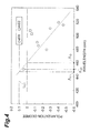
- Fig. 4 is a drawing showing a relation of peak emission wavelength versus polarization degree in the LED mode, with the typical inclination angles A OFF of 58 degrees (inclination with respect to the a-axis direction) and 62 degrees (inclination with respect to the m-axis direction).
- the polarization degree demonstrates 0.1 at a wavelength ⁇ L near the wavelength of 450 nm.
- the polarization degree becomes zero at a wavelength ⁇ 0 near 460 nm.
- a wavelength ⁇ S1 is 450 nm.
- the polarization degree P demonstrates wavelength dependence. Based on this experiment and other experiments by the inventors, the polarization degree P can be realized in the range of -1 ⁇ P ⁇ 0.1, in the range of peak lasing wavelength of not less than 450 nm and not more than 550 nm.
- the peak lasing wavelength of the multiple quantum well structure can be not less than 460 nm and not more than 550 nm.
- This semiconductor laser allows for realization of a low threshold. For example, with the inclination angles in the range of not less than 58 degrees and not more than 62 degrees, the polarization degree P is negative.
- Fig. 5 is a drawing showing cathodoluminescence (CL) images of LED structures.
- Fig. 5 (a) to Fig. 5 (d) show CL images of the respective LED structures with the off angle of 43 degrees with respect to the m-axis direction (polarization degree: 0.52), with the off angle of 58 degrees with respect to the a-axis direction (polarization degree: -0.29), with the off angle of 62 degrees with respect to the m-axis direction (polarization degree: -0.06), and with the off angle of 75 degrees with respect to the m-axis direction (polarization degree: 0.24).
- the acceleration voltage in measurement of the CL images was set so as to allow accelerated electrons to reach the InGaN layer.
- the polarization degree P decreases with increase in the emission peak wavelength.
- This behavior of polarization degree P can be explained as follows by increase in In composition of the well layers.
- the well layers with large In compositions are considered to have a strong quantum confinement effect.
- the results of Fig. 5 can also be explained by the increase in In composition of the well layers. Since the well layers with large In compositions impart significant stress to the interface between the InGaN layer and the n-type GaN layer, misfit dislocations are considered to be likely to occur at this interface.
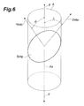
- Fig. 6 a part of the InGaN layer is shown as an object of a cylindrical shape.
- the c-plane slip plane S slip is inclined relative to the axis Ax to a direction indicated by normal vector N slip .
- the c-plane slip plane S slip slip slips in a direction indicated by slip vector D slip (the direction of the c-axis).
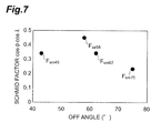
- Fig. 7 is a drawing showing a relation of off angle versus Schmid factor. Magnitudes of the Schmid factor are given in the following order. F Sa ⁇ 58 > F Sm ⁇ 62 > F Sm ⁇ 43 > F Sm ⁇ 75
- the order represented by Formula (2) qualitatively supports the relation of off angles with occurrence of the dark lines in the CL images.
- misfit dislocations are observed in the LED structure on the GaN substrate with 58 degrees with respect to the a-axis direction and in the LED structure on the GaN substrate with 62 degrees with respect to the m-axis direction. Boundaries of occurrence of misfit dislocations are angles of not more than 50 degrees and near 50 degrees and angles of not less than 70 degrees and near 70 degrees.
- Example 1 the relation of polarization degree versus angle was found by observation of emissions from the LED structures.
- Example 2 a semiconductor laser structure was made on a GaN wafer inclined at 58 degrees with respect to the a-axis direction.
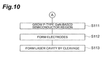
- the epitaxial growth was carried out by organometallic vapor-phase epitaxy and raw materials for the epitaxial growth used herein were trimethyl gallium (TMG), trimethyl indium (TMI), trimethyl aluminum (TMA), ammonia (NH 3 ), silane (SiH 4 ), and bis(cyclopentadienyl) magnesium (Cp 2 Mg). Fabrication of the epitaxial wafer and semiconductor laser shown in Fig. 8 by the following steps will be described with reference to Figs. 9 and 10 .
- Step S101 was to prepare a semipolar GaN wafer with the angle of inclination in the range of not less than 50 degrees and not more than 70 degrees.
- a GaN wafer 61 inclined at 58 degrees with respect to the a-axis direction was prepared.
- step S102 was to place the GaN wafer 61 on a susceptor of a growth reactor.
- step S103 was to carry out a thermal treatment at the temperature of 1050 Celsius degrees while supplying NH 3 and H 2 to the growth reactor, in order to carry out preprocessing.
- the time of the thermal treatment was, for example, 10 minutes.
- step S104 was carried out to change the substrate temperature, for example, to the temperature of 1150 Celsius degrees, in order to carry out growth of an n-type semiconductor.
- TMG TMA, NH 3 , and SiH 4 were supplied at the substrate temperature of 1150 Celsius degrees to the growth reactor, thereby growing a Si-doped AlGaN layer 62 on a primary surface 61a of the GaN wafer 61.
- the thickness of this AlGaN layer 62 is, for example, 2 micrometers.
- An Al composition of the AlGaN layer 62 is, for example, 0.04.
- Next step S105 was to grow an InCraN layer 63a on the AlGaN layer 62 while supplying TMG, TMI, and NH 3 at the substrate temperature of 840 Celsius degrees to the growth reactor.
- the thickness of the InGaN layer 63a is, for example, 100 nm and the In composition thereof, for example, 0.04.
- This InGaN layer 63a also functions as a optical guide layer.
- Step S106 was carried out to grow an active layer 64.
- a barrier layer growth step S107 was carried out to grow an undoped GaN barrier layer 65a while supplying TMG and NH 3 at the growth temperature (T B ) of 860 Celsius degrees to the growth reactor.
- the thickness of this GaN layer 65a is, for example, 15 nm.
- a well layer growth step S108 was carried out to grow an undoped InGaN well layer 65b on the GaN barrier layer 65a while supplying TMG, TMI, and NH 3 at the growth temperature (T W ) of 790 Celsius degrees to the growth reactor.
- the thickness of the InGaN well layer 65b was, for example, 3 nm.
- the In composition X of this In X Ga 1-X N was, for example, 0.18.
- the In composition X can be, for example, in the range of not less than 0.10 and not more than 0.40.
- the substrate temperature was changed from the growth temperature (T W ) to the growth temperature (T B ).
- the barrier layer growth step S 107 was carried out to grow an undoped GaN barrier layer 65a.
- the thickness of the GaN barrier layer 65a is, for example, 15 nm.
- a repetition step S109 was carried out to repeat the growth of the well layer 65b, the temperature change, and the growth of the barrier layer 65a, thereby forming the multiple quantum well structure including the GaN barrier layers 65a and InGaN well layers 65b arranged alternately.
- Next step S110 was to grow an InGaN layer 63b on the active layer 64 while supplying TMG, TMI, and NH 3 at the substrate temperature of 840 Celsius degrees to the growth reactor.
- the thickness of the InGaN layer is, for example, 100 nm and the In composition thereof, for example, 0.04.
- a p-type semiconductor growth step S111 was to grow a p-type GaN-based semiconductor region 66 on the InGaN layer 63b.
- supply of TMG was terminated and the substrate temperature was raised to 1000 Celsius degrees.
- TMG TMA, NH 3 , and C P2 Mg were supplied to the growth reactor to grow a p-type AlGaN electron block layer 66a on the InGaN optical guide layer 63b.
- This electron block layer 66a was, for example, 20 nm.
- the Al composition of the electron block layer 66a was, for example, 0.18.
- TMG TMA, NH 3 , and C P2 Mg were supplied to the growth reactor to grow a p-type AlGaN cladding layer 66b on the electron block layer 66a.
- This p-type cladding layer 66b was, for example, 400 nm.
- the Al composition of the p-type cladding layer 66b was, for example, 0.04.
- the supply of TMA was terminated and a p-type GaN contact layer 66c was grown on the p-type cladding layer 66b.
- the p-type GaN contact layer 66c was, for example, 50 nm.
- the temperature of the growth reactor was decreased to room temperature, thereby fabricating an epitaxial wafer E LD .
- An electrode forming step S112 is to form an insulating film 68 with a contact window on the epitaxial wafer E LD and thereafter to form a p-side electrode 69a and an n-side electrode 69b on the epitaxial wafer E LD .
- a p-side transparent electrode (Ni/Au) is formed on the p-type GaN contact layer 66c. After this, an anode pad electrode (Ti/Au) is formed.
- the insulating film is, for example, a silicon oxide film.
- the contact window is, for example, a stripe shape with the width of 10 ⁇ m.
- a cathode electrode (Ti/Al) is formed on a back surface 61 b of the GaN wafer 61. After this, the electrodes are annealed (for example, at 55 Celsius degrees for one minute). A substrate product of semiconductor light emitting device was obtained through these steps.
- a cleavage step S 113 was carried out to cleave the substrate product with a predetermined space, thereby making a laser cavity.
- the cleavage causes, for example, the laser cavity to include a pair of m-plane cleaved faces.
- a semiconductor laser D M was fabricated through these steps.
- the same laser structure was also made on a c-plane GaN wafer by epitaxial growth.
- a semiconductor laser D C was fabricated.
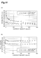
- Fig. 11 is a drawing showing characteristics of the semiconductor lasers D M and D C .
- Fig. 11 (a) shows a relation of injected current density versus peak wavelength of emission spectra in the LED mode.
- Fig. 11 (b) shows a relation of injected current density versus half maximum full-width of emission spectra in the LED mode.
- the semiconductor laser D M is made on a semipolar plane (plane inclined at 58 degrees with respect to the a-axis direction), a blue shift of the semiconductor laser D M is smaller than that of the semiconductor laser D C .
- the half maximum full-width of the semiconductor laser D M is also smaller than that of the semiconductor laser D C .
- the behavior of the half maximum full-width can be understood as follows. Since the semiconductor laser D C demonstrates the significant piezoelectric effect, carrier densities in the respective well layers of the active layer differ according to an amount of injected current into the active layer. The difference of carrier densities causes a difference in levels of piezoelectric screening in the respective well layers. For this reason, the half maximum full-width becomes larger in the emission spectrum in the LED mode.
- the piezoelectric polarization of the semiconductor laser D M is smaller than that of the semiconductor laser D C , and therefore the difference in levels of piezoelectric screening in the respective well layers is small.
- the well layers of the semiconductor laser D M demonstrate less non-uniformity of In composition than those of the semiconductor laser D C . This uniformity of In composition also contributes to reduction in half maximum full-width in the emission spectrum in the LED mode.
- the semiconductor laser D M showed the polarization degree of +0.02 when measured with the injected current of 5 mA. This polarization degree is smaller than those in hitherto reported examples.
- the semiconductor laser D M lased at the current of 850 mA.
- the semiconductor laser D C lased at the current of 900 mA.
- the semiconductor lasers were obtained with the very small polarization degree (not more than 0.1 and not less than -1). It is considered that the lower threshold than in the comparative example was achieved using the end face mirrors by m-plane cleavage.
Landscapes
- Physics & Mathematics (AREA)
- Optics & Photonics (AREA)
- Chemical & Material Sciences (AREA)
- Engineering & Computer Science (AREA)
- Nanotechnology (AREA)
- Condensed Matter Physics & Semiconductors (AREA)
- General Physics & Mathematics (AREA)
- Electromagnetism (AREA)
- Life Sciences & Earth Sciences (AREA)
- Biophysics (AREA)
- Crystallography & Structural Chemistry (AREA)
- Semiconductor Lasers (AREA)
Applications Claiming Priority (2)
| Application Number | Priority Date | Filing Date | Title |
|---|---|---|---|
| JP2009034004A JP4775455B2 (ja) | 2009-02-17 | 2009-02-17 | Iii族窒化物半導体レーザ、及びiii族窒化物半導体レーザを作製する方法 |
| PCT/JP2009/071661 WO2010095340A1 (ja) | 2009-02-17 | 2009-12-25 | Iii族窒化物半導体レーザ、及びiii族窒化物半導体レーザを作製する方法 |
Publications (1)
| Publication Number | Publication Date |
|---|---|
| EP2400604A1 true EP2400604A1 (en) | 2011-12-28 |
Family
ID=42633632
Family Applications (1)
| Application Number | Title | Priority Date | Filing Date |
|---|---|---|---|
| EP09840443A Withdrawn EP2400604A1 (en) | 2009-02-17 | 2009-12-25 | Iii nitride semiconductor laser and method for manufacturing iii nitride semiconductor laser |
Country Status (7)
| Country | Link |
|---|---|
| US (1) | US8548021B2 (enExample) |
| EP (1) | EP2400604A1 (enExample) |
| JP (1) | JP4775455B2 (enExample) |
| KR (1) | KR101269315B1 (enExample) |
| CN (1) | CN102318152B (enExample) |
| TW (1) | TW201034325A (enExample) |
| WO (1) | WO2010095340A1 (enExample) |
Families Citing this family (14)
| Publication number | Priority date | Publication date | Assignee | Title |
|---|---|---|---|---|
| US7933303B2 (en) | 2009-06-17 | 2011-04-26 | Sumitomo Electric Industries, Ltd. | Group-III nitride semiconductor laser device, and method for fabricating group-III nitride semiconductor laser device |
| JP5206699B2 (ja) | 2010-01-18 | 2013-06-12 | 住友電気工業株式会社 | Iii族窒化物半導体レーザ素子、及びiii族窒化物半導体レーザ素子を作製する方法 |
| JP2011018784A (ja) * | 2009-07-09 | 2011-01-27 | Sony Corp | 半導体レーザ素子及びその駆動方法、並びに、半導体レーザ装置 |
| JP2011023537A (ja) * | 2009-07-15 | 2011-02-03 | Sumitomo Electric Ind Ltd | Iii族窒化物半導体素子、エピタキシャル基板、及びiii族窒化物半導体素子を作製する方法 |
| TWI560963B (en) * | 2010-03-04 | 2016-12-01 | Univ California | Semi-polar iii-nitride optoelectronic devices on m-plane substrates with miscuts less than +/- 15 degrees in the c-direction |
| US8189639B2 (en) * | 2010-05-28 | 2012-05-29 | Corning Incorporated | GaN-based laser diodes with misfit dislocations displaced from the active region |
| JP5139555B2 (ja) * | 2011-04-22 | 2013-02-06 | 住友電気工業株式会社 | 窒化物半導体レーザ、及びエピタキシャル基板 |
| CN102227046A (zh) * | 2011-05-25 | 2011-10-26 | 北京化工大学 | 一种氮化镓基半导体激光器及其制作方法 |
| US20130100978A1 (en) * | 2011-10-24 | 2013-04-25 | The Regents Of The University Of California | Hole blocking layer for the prevention of hole overflow and non-radiative recombination at defects outside the active region |
| WO2015190171A1 (ja) * | 2014-06-10 | 2015-12-17 | ソニー株式会社 | 半導体光デバイス及びその製造方法並びに半導体光デバイス組立体 |
| KR102390624B1 (ko) | 2015-06-05 | 2022-04-26 | 오스텐도 테크놀로지스 인코포레이티드 | 다수의 활성층들로 선택적으로 캐리어를 주입한 발광 구조체 |
| US10396240B2 (en) * | 2015-10-08 | 2019-08-27 | Ostendo Technologies, Inc. | III-nitride semiconductor light emitting device having amber-to-red light emission (>600 nm) and a method for making same |
| DE112019003671T5 (de) | 2018-07-20 | 2021-04-08 | Sony Semiconductor Solutions Corporation | Halbleiterlichtemissionselement |
| JP7422496B2 (ja) * | 2019-06-21 | 2024-01-26 | 古河機械金属株式会社 | 構造体、光デバイス、光デバイスの製造方法、構造体の製造方法 |
Family Cites Families (9)
| Publication number | Priority date | Publication date | Assignee | Title |
|---|---|---|---|---|
| JP3206316B2 (ja) * | 1994-08-12 | 2001-09-10 | 松下電器産業株式会社 | 半導体レーザ |
| JP2005072368A (ja) | 2003-08-26 | 2005-03-17 | Sony Corp | 半導体発光素子、半導体レーザ素子、及び画像表示装置 |
| US7408199B2 (en) * | 2004-04-02 | 2008-08-05 | Nichia Corporation | Nitride semiconductor laser device and nitride semiconductor device |
| US7751455B2 (en) * | 2004-12-14 | 2010-07-06 | Palo Alto Research Center Incorporated | Blue and green laser diodes with gallium nitride or indium gallium nitride cladding laser structure |
| JP5113446B2 (ja) * | 2006-08-11 | 2013-01-09 | 三洋電機株式会社 | 半導体素子およびその製造方法 |
| WO2008100504A1 (en) | 2007-02-12 | 2008-08-21 | The Regents Of The University Of California | Cleaved facet (ga,al,in)n edge-emitting laser diodes grown on semipolar {11-2n} bulk gallium nitride substrates |
| JP2009016684A (ja) * | 2007-07-06 | 2009-01-22 | Nichia Corp | 半導体レーザ素子 |
| JP2009021346A (ja) | 2007-07-11 | 2009-01-29 | Rohm Co Ltd | 半導体発光素子 |
| JP5286723B2 (ja) * | 2007-09-14 | 2013-09-11 | 国立大学法人京都大学 | 窒化物半導体レーザ素子 |
-
2009
- 2009-02-17 JP JP2009034004A patent/JP4775455B2/ja not_active Expired - Fee Related
- 2009-12-25 CN CN2009801569816A patent/CN102318152B/zh not_active Expired - Fee Related
- 2009-12-25 WO PCT/JP2009/071661 patent/WO2010095340A1/ja not_active Ceased
- 2009-12-25 KR KR1020117020627A patent/KR101269315B1/ko not_active Expired - Fee Related
- 2009-12-25 EP EP09840443A patent/EP2400604A1/en not_active Withdrawn
- 2009-12-31 TW TW098146573A patent/TW201034325A/zh unknown
-
2011
- 2011-08-17 US US13/211,858 patent/US8548021B2/en not_active Expired - Fee Related
Non-Patent Citations (1)
| Title |
|---|
| See references of WO2010095340A1 * |
Also Published As
| Publication number | Publication date |
|---|---|
| WO2010095340A1 (ja) | 2010-08-26 |
| KR101269315B1 (ko) | 2013-05-29 |
| US8548021B2 (en) | 2013-10-01 |
| JP4775455B2 (ja) | 2011-09-21 |
| KR20110112472A (ko) | 2011-10-12 |
| JP2010192594A (ja) | 2010-09-02 |
| TW201034325A (en) | 2010-09-16 |
| CN102318152A (zh) | 2012-01-11 |
| US20120008660A1 (en) | 2012-01-12 |
| CN102318152B (zh) | 2013-06-05 |
Similar Documents
| Publication | Publication Date | Title |
|---|---|---|
| US8548021B2 (en) | III-nitride semiconductor laser, and method for fabricating III-nitride semiconductor laser | |
| US8067257B2 (en) | Nitride based semiconductor optical device, epitaxial wafer for nitride based semiconductor optical device, and method of fabricating semiconductor light-emitting device | |
| JP5003527B2 (ja) | Iii族窒化物発光素子、及びiii族窒化物系半導体発光素子を作製する方法 | |
| US8488642B2 (en) | Gallium nitride based semiconductor light-emitting device and method for fabricating the same, gallium nitride based light-emitting diode, epitaxial wafer, and method for fabricating gallium nitride light-emitting diode | |
| US8718110B2 (en) | Nitride semiconductor laser and epitaxial substrate | |
| US20110309328A1 (en) | Nitride semiconductor light emitting device, epitaxial substrate, and method for fabricating nitride semiconductor light emitting device | |
| US20110212560A1 (en) | Method for fabricating nitride semiconductor light emitting device and method for fabricating epitaxial wafer | |
| JP4450112B2 (ja) | 窒化物系半導体光素子 | |
| US8803274B2 (en) | Nitride-based semiconductor light-emitting element | |
| KR20100099066A (ko) | 질화갈륨계 반도체 광소자, 질화갈륨계 반도체 광소자를 제조하는 방법 및 에피택셜 웨이퍼 | |
| US8748868B2 (en) | Nitride semiconductor light emitting device and epitaxial substrate | |
| JP5332959B2 (ja) | 窒化物系半導体光素子 | |
| JP2009224602A (ja) | 窒化物半導体レーザ、窒化物半導体レーザを作製する方法、及び窒化物半導体レーザのためのエピタキシャルウエハ | |
| WO2014088030A1 (ja) | 窒化物半導体発光素子、窒化物半導体発光素子を作製する方法 | |
| JP5379216B2 (ja) | Iii族窒化物半導体レーザ | |
| JP4404164B1 (ja) | 半導体発光素子を製造する方法 | |
| JP2011188000A (ja) | Iii族窒化物半導体レーザ、及びiii族窒化物半導体レーザを作製する方法 | |
| JP2012109624A (ja) | Iii族窒化物発光素子、及びiii族窒化物系半導体発光素子を作製する方法 |
Legal Events
| Date | Code | Title | Description |
|---|---|---|---|
| PUAI | Public reference made under article 153(3) epc to a published international application that has entered the european phase |
Free format text: ORIGINAL CODE: 0009012 |
|
| 17P | Request for examination filed |
Effective date: 20110914 |
|
| AK | Designated contracting states |
Kind code of ref document: A1 Designated state(s): AT BE BG CH CY CZ DE DK EE ES FI FR GB GR HR HU IE IS IT LI LT LU LV MC MK MT NL NO PL PT RO SE SI SK SM TR |
|
| RIN1 | Information on inventor provided before grant (corrected) |
Inventor name: ENYA YOHEI Inventor name: FUJII KEI Inventor name: AKITA KATSUSHI Inventor name: YOSHIZUMI YUSUKE Inventor name: KYONO TAKASHI Inventor name: SUMITOMO TAKAMICHI Inventor name: UENO MASAKI |
|
| DAX | Request for extension of the european patent (deleted) | ||
| STAA | Information on the status of an ep patent application or granted ep patent |
Free format text: STATUS: THE APPLICATION HAS BEEN WITHDRAWN |
|
| 18W | Application withdrawn |
Effective date: 20150312 |