WO2010092750A1 - 波面収差測定方法及びその装置 - Google Patents
波面収差測定方法及びその装置 Download PDFInfo
- Publication number
- WO2010092750A1 WO2010092750A1 PCT/JP2010/000345 JP2010000345W WO2010092750A1 WO 2010092750 A1 WO2010092750 A1 WO 2010092750A1 JP 2010000345 W JP2010000345 W JP 2010000345W WO 2010092750 A1 WO2010092750 A1 WO 2010092750A1
- Authority
- WO
- WIPO (PCT)
- Prior art keywords
- lens
- shack
- inspected
- hartmann sensor
- light source
- Prior art date
- Legal status (The legal status is an assumption and is not a legal conclusion. Google has not performed a legal analysis and makes no representation as to the accuracy of the status listed.)
- Ceased
Links
Images






Classifications
-
- G—PHYSICS
- G01—MEASURING; TESTING
- G01M—TESTING STATIC OR DYNAMIC BALANCE OF MACHINES OR STRUCTURES; TESTING OF STRUCTURES OR APPARATUS, NOT OTHERWISE PROVIDED FOR
- G01M11/00—Testing of optical apparatus; Testing structures by optical methods not otherwise provided for
- G01M11/02—Testing optical properties
- G01M11/0242—Testing optical properties by measuring geometrical properties or aberrations
- G01M11/0257—Testing optical properties by measuring geometrical properties or aberrations by analyzing the image formed by the object to be tested
-
- G—PHYSICS
- G01—MEASURING; TESTING
- G01M—TESTING STATIC OR DYNAMIC BALANCE OF MACHINES OR STRUCTURES; TESTING OF STRUCTURES OR APPARATUS, NOT OTHERWISE PROVIDED FOR
- G01M11/00—Testing of optical apparatus; Testing structures by optical methods not otherwise provided for
- G01M11/02—Testing optical properties
- G01M11/0207—Details of measuring devices
Definitions
- the present invention relates to a method and apparatus for measuring wavefront aberration of a lens mounted on an optical apparatus such as a semiconductor optical inspection apparatus or a printed board laser processing apparatus.
- the semiconductor wafer optical inspection device is a device for detecting foreign matter on the wafer and managing the number of foreign matters. Since the size of foreign matter to be managed differs according to the semiconductor manufacturing process, the inspection apparatus has an optical magnification variable function. When the optical magnification is increased, smaller foreign objects can be detected, but on the other hand, the field of view that can be detected by the sensor is also reduced, so the throughput is reduced. Therefore, in a semiconductor line, inspection is performed with an enlarged magnification only in a process that requires particularly fine foreign matter management.
- the detection system of the inspection apparatus is composed of an objective lens and an imaging lens, and the magnification change is generally performed by changing the focal length of the imaging lens.
- a large number of wafer manufacturing lines use multiple optical inspection devices.
- an allowable value of the number of foreign matters is set in advance, and when the allowable value is exceeded, countermeasures such as cleaning of the manufacturing apparatus are taken.
- the optical inspection apparatuses A and B have different sensitivities (detectable foreign substance sizes)
- an allowable value must be set for each inspection apparatus, which is a major obstacle to the operation of the inspection apparatus.
- the sensitivity of the optical inspection device largely depends on the imaging performance of the detection system lens. Therefore, in order to reduce the difference in sensitivity of the optical inspection apparatus, it is necessary to manage the imaging performance of the lens alone, particularly the wavefront aberration.
- Patent Document 1 Japanese Patent Laid-Open No. 2004-14764.
- the Shack-Hartmann sensor is a sensor that divides and condenses the wavefront (phase distribution) of light incident on the sensor with an array lens, and picks it up with a two-dimensional sensor as an array image of multiple spots. An aberration coefficient is calculated.
- Patent Document 1 Japanese Patent Laid-Open No. 2004-14764
- Patent Document 2 Japanese Patent Laid-Open No. 2006-30016
- Wavefront aberration measurement using the Shack-Hartmann sensor is less susceptible to environmental changes such as air temperature changes and vibrations in the optical path, and can also handle local wavefront changes beyond the measurement wavelength caused by aspherical lenses. This is advantageous compared with the conventional interferometer method.
- the projection lens of the exposure apparatus is the measurement object.
- the lens of the detection system of the optical inspection apparatus is composed of an objective lens and an imaging lens.
- the focal length of the imaging lens changes due to variable magnification. This is realized by replacing the imaging lens or using a zoom lens.
- the wavefront aberration can be measured with one set of objective lens and imaging lens, like a projection lens, but the obtained aberration is the positive aberration generated by the objective lens and the negative aberration of the imaging lens. The result may have been canceled at In this case, if the lens is changed to an imaging lens having a different focal length, the aberration may change greatly. Therefore, it is desirable to measure the aberration of the objective lens alone. Since the objective lens alone does not form an image (it is an infinite system), a measurement method with a configuration different from the above known example is required.
- an infinite system f ⁇ lens is used as well as the objective lens of the semiconductor optical inspection apparatus.
- parallel light is deflected by a galvanometer mirror installed at the pupil position of an f ⁇ lens and incident on the f ⁇ lens, thereby scanning the printed circuit board with a condensed beam.
- the f ⁇ lens is a lens that is intentionally distorted so that the beam position on the printed circuit board is determined by the product f ⁇ of the light deflection angle ⁇ by the galvano mirror and the focal length of the f ⁇ lens. Since the f ⁇ lens is not an imaging lens, a measurement method different from the conventional imaging type is required.
- the aberration of the f ⁇ lens affects the processing shape for each scanning position of the focused beam. Therefore, in order to obtain a uniform processing shape in the scanning range, it is necessary to manage the aberration (wavefront aberration). .
- Patent Document 2 Japanese Patent Application Laid-Open No. 2006-30016
- only the lens to be measured is measured twice by changing its posture, such as rotating, and the difference between the measured values is obtained, whereby the aberration of the measurement optical system is determined.
- a method for canceling and calculating the aberration of only the lens to be measured is disclosed.
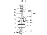
- FIG. 12 shows a configuration in the case where the wavefront aberration of the infinite objective lens 2 is measured by the Shack-Hartmann sensor 4.
- the light condensed at the point A by the condenser lens 10 enters the objective lens 2 and becomes parallel light, and then enters the pupil (aperture) 21, and then includes a relay lens 301 and a relay lens 302. After being condensed through the relay lens 300, it is converted into parallel light and detected by the Shack-Hartmann sensor 4.
- the relay lens 300 forms an image of the pupil 21 on the Shack-Hartmann sensor 4.
- the condenser lens 10 condenses the light at a point A at a distance L from the optical axis, and this point is used as a measurement point for wavefront aberration measurement.
- the angle ⁇ of the parallel light 410 incident on the pupil 21 is determined by using the focal length f1 and the distance L of the objective lens 2.
- the reduction magnification M of the relay lens 300 needs to satisfy the following expression because the diameter Dep of the pupil 21 is detected in the detection area S of the Shack-Hartmann sensor 4.
- M ⁇ S / Dep (Expression 2)
- the angle ⁇ incident on the Shack-Hartmann sensor 4 is obtained by the following equation.
- FIG. 13 is a view showing the inside of the Shack-Hartmann sensor 4.
- the wavefront 400 incident on the Shack-Hartmann sensor 4 is divided by the array lens 41.
- the light beam 401 incident on the position ( ⁇ , ⁇ ) of the wavefront 400 is condensed at a position shifted by ⁇ X ( ⁇ , ⁇ ) from the position ( ⁇ , ⁇ ) on the two-dimensional sensor 42 by the following equation. Is done.
- W is the phase distribution of the wavefront
- f4 is the focal length of the array lens 41.
- the measurable wavefront inclination ⁇ needs to be about 3 degrees or less in order for the array lens 41 to be imaged as a spot on the two-dimensional sensor 42. Therefore, as described above, when the incident angle to the Shack-Hartmann sensor 4 is 18.4 degrees, the condition of about 3 degrees or less is not satisfied and measurement is impossible. That is, the wavefront aberration of the objective lens 2 cannot be measured by a general method in which the pupil 21 of the objective lens 2 is imaged on the Shack-Hartmann sensor 4 by the relay lens 300. Accordingly, an object of the present invention is to provide a technique for measuring wavefront aberration that clears the incident angle limitation on the Shack-Hartmann sensor when using a relay lens.
- Patent Document 2 Japanese Patent Laid-Open No. 2006-30016
- the measurement is performed twice by rotating 90 degrees, and the difference between the positional deviations on the Shack-Hartmann sensor is obtained.
- the difference is zero and the aberration cannot be calculated. Therefore, another object of the present invention is to provide a measurement method capable of correcting the aberration of the measurement optical system even for rotationally symmetric aberration.
- a Shack-Hartmann sensor is directly installed at the pupil position of the objective lens without using a relay lens. Thereby, the incident angle to the Shack-Hartmann sensor can be reduced.
- the Shack-Hartmann sensor is tilted in the wavefront tilt direction. Thereby, the incident angle limit of 3 degrees or less to the Shack-Hartmann sensor can be cleared.
- the entire pupil diameter is covered by scanning the Shack-Hartmann sensor.
- a scanning method of the Shack-Hartmann sensor there are a method of scanning a two-dimensional sensor two-dimensionally by step and repeat, and a method of scanning one-dimensionally by a one-dimensional sensor that covers the pupil diameter.
- the pitching and yawing of the scanning stage affects the error of the spot focusing position during the entire pupil synthesis
- the pitching and yawing of the scanning stage are measured with a three-axis laser length measuring instrument or an autocollimator. Is a method for correcting.
- the pitch deviation and yawing of the scanning stage are errors
- the error is corrected by measuring with a two-axis laser length measuring device.
- Another invention that clears the limit on the incident angle to the Shack-Hartmann sensor is to correct the tilt of the wavefront at the pupil position at the edge of the field of view with a galvanometer mirror installed at the pupil position.
- the incident angle ⁇ to the Shack-Hartmann sensor is always set to zero.
- the incident angle limitation can be cleared even if the pupil is reduced by the relay lens so as to be within the sensor detection field.
- a spherical wave generated by a point light source is directly measured by a Shack-Hartmann sensor without passing through another optical system. Measure the displacement data, and subtract this data from the measurement data for the objective lens. As a result, the wavefront aberration of only the objective lens can be calculated, and the rotationally symmetric wavefront aberration, which was impossible in the conventional example, can be measured with high accuracy.
- the wavefront aberration of the infinite objective lens can be measured by the Shack-Hartmann sensor, and the measurement is less affected by the environment than the conventional interferometer. Is possible.
- the wavefront aberration of the Shack-Hartmann sensor with a point light source, it is possible to measure the wavefront aberration with high accuracy only for the lens to be measured.
- the foreign matter detection sensitivity and processing shape of semiconductor optical inspection equipment and printed circuit board laser processing equipment are made uniform, and the operational efficiency of multiple optical inspection equipment in the semiconductor line is improved.
- the effect of improving the quality of laser processing can be obtained.
- FIG. 1 is a front cross-sectional view showing a schematic configuration of a wavefront aberration measuring apparatus according to a first embodiment. It is a top view of the pupil surface which shows the mode of the imaging of the two-dimensional sensor on the pupil of an objective lens in a 1st Example.
- 3 is a plan view of a pupil plane showing a relationship between a rotary stage 22 on which an objective lens 2 is mounted and a condensing point A.
- FIG. FIG. 3 is a front cross-sectional view showing a schematic configuration of a wavefront aberration measuring apparatus when measuring aberration of an array lens.
- FIG. 6 is a front cross-sectional view showing a schematic configuration of a wavefront aberration measuring apparatus according to a second embodiment of the present invention.
- FIG. 6 is a front cross-sectional view showing a schematic configuration of a wavefront aberration measuring apparatus according to a third embodiment of the present invention.
- FIG. 10 is a front cross-sectional view showing a schematic configuration of a wavefront aberration measuring apparatus according to a fourth embodiment of the present invention. It is a schematic sectional drawing of the front of the optical system which shows schematic structure for measuring the wavefront aberration of an objective lens via a relay lens. It is sectional drawing of the plane of a Shack-Hartmann sensor which shows the position condensed on a two-dimensional sensor by an array lens when there exists a local inclination in a wave front.
- the Shack-Hartmann sensor In a Shack-Hartmann measurement device that measures the wavefront aberration of an infinite objective lens using a point light source, the Shack-Hartmann sensor is tilted so that it is parallel to the wavefront according to the position of the point light source at the pupil position of the objective lens. , Scan. Pitching and yawing during scanning are corrected to obtain the focused spot position, thereby calculating the wavefront aberration coefficient.
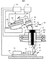
- FIG. 1 is an overall configuration diagram of this embodiment.
- 11 is a light source that emits parallel light
- 12 is a beam expander
- 10 is a condensing lens
- 13 is a folding mirror that bends the optical path of light that has passed through the beam expander 12 in the direction of the condensing lens 10.
- Reference numeral 14 denotes a stage having a configuration in which the light source 11, the beam expander 12, the bending mirror 13, and the condenser lens 10 are placed and can move in at least one axial direction.
- 2 is an objective lens
- 22 is a rotary stage that can rotate while holding the objective lens 2
- 221 is an attachment member that fixes the objective lens 2 to the rotary stage 22.
- the rotary stage 22 can be retracted to a position completely deviated from the optical axis of the moving condenser lens 10 in a direction perpendicular to the drawing by a driving mechanism (not shown) while holding the objective lens 2.
- 4 is a Shack-Hartmann sensor
- 41 is a large number of minute lenses 4101, 4102, 4103, 4104 in the plane (four examples are shown in FIG. 1, but a larger number of minute lenses may be arranged).
- the array lens is arranged in an array, 42 is a two-dimensional sensor, 43 is a stage movable at least in one axial direction, 44 is a gonio stage, and 431 is a support member fixed to the stage 43 to support the Shack-Hartmann sensor 4. ing.
- the gonio stage 44 is instructed to be movable in the vertical direction of the drawing on a Z stage (not shown).
- a control system 51 controls the stage 14, the rotary stage 22, the gonio stage 44, and the stage 43.
- a processing system 52 processes the output signal from the two-dimensional sensor 42 of the Shack-Hartmann sensor 4 using the control signal of the control system 51.
- the parallel light emitted from the light source 11 mounted on the stage 14 is expanded by the beam expander 12 and then condensed at the measurement point A by the condenser lens 10.
- the light emitted from the point A is incident on the objective lens 2 which is a lens to be measured, becomes parallel light 410 inclined according to the position of the point A, and the Shack-Hartmann sensor 4 installed on the pupil 21 of the objective lens 2. Is incident on.
- the inclination angle ⁇ of the Shack-Hartmann sensor 4 is obtained from the focal length f1 of the objective lens 2 and the distance L between the optical axis and the point A by using the above (Equation 1).
- the tilt angle ⁇ is calculated by the control system 51 by obtaining the position of the stage 14 and controls the gonio stage 44 so as to have the tilt angle ⁇ .
- a part of the parallel light 410 is divided by the array lens 41 and is imaged as a condensed spot on the two-dimensional sensor 42 according to the inclination of the wavefront of each part.
- control system 51 drives the stage 43 to move the Shack-Hartmann sensor 4 to the next imaging position on the surface that forms the tilt angle ⁇ with the pupil 21 and images another part of the parallel light 410. By repeating this operation, the entire pupil 21 is imaged.
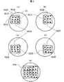
- FIG. 2A shows an imaging range 4210 by the two-dimensional sensor 42 on the area of the pupil 21 when the stage 43 is at the first position.
- FIGS. 2B, 2C, and 2D show imaging ranges 4220, 4230, and 4240 when the stage 43 is in the second, third, and fourth positions.
- the imaging ranges 4210, 4220, 4230, and 4240 at the first to fourth positions are set so that the partial areas overlap each other.
- the intersection 4202 indicates the focused spot position in design (ideal state) of each microlens constituting the array lens 41.
- the actual focused spot 4211 is displaced from this position due to aberration.
- the processing system 52 calculates the center of gravity position of the focused spot in each image, and then rotates and translates each spot array so that the coordinates of the overlapping spot arrays 4213, 4214, 4224, and 4233 in each image match.
- a combined spot array 450 is obtained after correcting the positional deviation as shown in FIG. In this way, yawing and pitching at the time of movement by the stage 43 are corrected by combining by rotational movement and parallel movement.
- the function of the rotary stage 22 on which the objective lens 2 is mounted will be described with reference to FIG. Since the wavefront aberration of the objective lens 2 varies depending on the measurement point A (the condensing point A of the condensing lens 10), which is a relative position of the objective lens 2 with respect to the optical axis 200, the wavefront aberration is measured over the entire area in the field of view of the objective lens 2. There is a need.
- the gonio stage 44 is a uniaxial tilt stage, and the tilt angle is controlled with respect to the position of the measurement point A in the specific radial direction of the objective lens 2.
- the objective lens 2 is rotated by the rotary stage 22. For example, when the control system 51 rotates the rotary stage 22 every 22.5 degrees, it is possible to measure almost the entire visual field of the objective lens 2.
- a plurality of measurement points 2001 in the direction along the axis 2001 is obtained by sequentially inclining the gonio stage 44 in one axis direction with the rotary stage 22 fixed at a certain position.
- 2001, 20013... 2001n wavefront aberration is measured, and then the rotary stage 22 is rotated 22.5 degrees and then the gonio stage 44 is similarly inclined sequentially in one axial direction.
- the wavefront aberration can be measured over almost the entire region of the visual field 201 of the objective lens 2.
- the control system 51 drives the Z stage 46 that can move in the vertical direction of the drawing to diverge from the measurement point A.
- the spherical wave 100 is moved to a position where it enters the entire array lens 41.
- the array lens array 41 is set to (i, j) with the center of the array lens 41 being (0, 0), the distance from the measurement point A to the array lens 41 is R, and the pitch of the array lens in the X and Y directions is Assuming ⁇ Px and ⁇ Py, ideal values ⁇ X0 (i, j) and ⁇ Y0 (i, j) on the lattice points of the focusing spot of the (i, j) th array lens are given by the following equations.
- f4 is the focal length of the array lens 41.
- the positional deviations of the focused spot actually measured by the two-dimensional sensor 42 are ⁇ Xs (i, j) and ⁇ Ys (i, j)
- the positional deviations ⁇ Xa (i, j) and ⁇ Ya caused by the aberration of the array lens 41 (I, j) is obtained by the following equation.
- ⁇ Xa (i, j) ⁇ Xs (i, j) ⁇ X0 (i, j) (Equation 8)
- ⁇ Ya (i, j) ⁇ Ys (i, j) ⁇ Y0 (i, j) (Equation 9)
- the processing system 52 stores the values of ⁇ Xa (i, j) and ⁇ Ya (i, j), and the focused spot position deviations ⁇ X (i, j) and ⁇ Y (i) at the time of measurement of the objective lens 2 described above. , J) is corrected by the following equation.
- FIG. 5 shows the configuration of a wavefront aberration measuring apparatus that corrects errors caused by yawing and pitching of the stage 23.
- the basic configuration is the same as that of the first embodiment shown in FIG. 1, and the same parts are denoted by the same reference numerals.
- This embodiment differs from the first embodiment shown in FIG. 1 in that an autocollimator 45 is attached to a stage 43 placed on a gonio stage 44.
- the autocollimator 45 measures the yawing angle ⁇ and the pitching angle ⁇ of the stage 43 and sends a signal to the processing system 52.
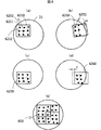
- FIGS. 6A to 6E show the state of imaging when a yawing error ⁇ and a pitching error ⁇ occur.
- the states shown in FIGS. 6A to 6D are basically the same as the imaging conditions shown in FIGS. 2A to 2D.
- region of the pupil 21 of the objective lens 2 when is in the 1st position is shown.
- FIGS. 6B, 6 ⁇ / b> C, and 6 ⁇ / b> D show imaging ranges 6220, 6230, and 6240 when the stage 43 is in the second, third, and fourth positions.
- the intersection point 6202 indicates the focused spot position in the design (ideal state) of each microlens (4101, 4102, 4103, 4104 shown in FIG. 1) that constitutes the array lens 41.
- the actual focused spot 6211 (the position indicated by ⁇ in FIGS. 6A to 6D) deviates from this position due to aberration.
- the processing system 52 that has received the signal from the autocollimator 45 converts the coordinates by the following equation using the measured yawing error ⁇ , corrects the deviation of the imaging range 6250 as shown in FIG. Correct.
- the spot arrangement error in the image obtained by imaging at each position of the stage 43 can be corrected, and by combining the individual images of this error, As shown in FIG. 6E, it is possible to obtain a combined spot array 650 with the positional deviation corrected.
- FIG. 8 shows another apparatus configuration for acquiring the image of the pupil 21.
- the same components as those in the first embodiment are given the same numbers.
- the third embodiment is different from the first and second embodiments in that the lens array 411 is fixed and the entire surface of the pupil 21 of the objective lens 2 is covered. That is, the lens array 411 is configured by arranging a large number of microlenses 4111, 4112, 4113... In a region covering the entire surface of the pupil 21 of the objective lens 2, and the lens array 411 is fixed to the fixing member 432.
- the gonio stage 44 is fixed, and the one-dimensional sensor 421 is scanned in one direction to pick up the respective condensing spots by the microlenses 4111, 4112, 4113.
- the one-dimensional sensor 421 has an imaging range equal to or larger than the diameter of the pupil 21 in a direction perpendicular to the paper surface in FIG. 8 and is mounted on the one-axis stage 430.
- the moving distance of the single axis stage 430 is measured by a laser length measuring device 451.
- the one-axis stage 430 is driven by the control system 51, and the processing system 52 combines the one-dimensional image picked up by the lens array 411 into a two-dimensional image based on the position signal of the laser length measuring device 451.
- FIG. 9 shows the locus of the imaging region 4215 of the one-dimensional sensor 421.
- FIG. 10 shows a plan view of the single-axis stage 430.
- the laser length measuring device 451 can measure the yawing angle ⁇ of the uniaxial stage 430 because it measures with a biaxial beam.
- the processing system 52 corrects the rotation error 4217 of the imaging area at the time of image composition from the measured yawing angle ⁇ .
- the uniaxial stage 430 is not a highly accurate stage, it is possible to accurately measure the wavefront aberration.
- the one-dimensional sensor 421 is used, the influence of the pitching of the one-axis stage 430 remains within one pixel in the scanning direction, and therefore there is almost no influence on the wavefront aberration measurement accuracy.
- FIG. 11 shows the configuration of a wavefront aberration measuring apparatus that always corrects the inclination of the wavefront that occurs when the measurement point A is off-axis in a fixed direction.
- the same components as those in the first embodiment are given the same numbers.
- the galvanometer mirror 60 can be installed at the position of the pupil plane 211.
- the control system 511 calculates a distance L from the position signal of the stage 14 (a signal obtained by detecting the position of the stage 14 with a position sensor such as a laser length measuring device (not shown)) to the optical axis of the measurement point A. Then, using (Equation 1), the inclination angle ⁇ (see FIG. 1) of the wavefront at the pupil plane is obtained, and the angle ⁇ of the galvanometer mirror 60 is controlled so that the reflected light 601 is always directed in the direction of the optical axis 600. .
- the reflected light 601 can be controlled to be directed in the direction of the optical axis 600 by tilting the galvanometer mirror by ⁇ / 2 with respect to the tilt angle ⁇ .
- the reflected light 601 enters the Shack-Hartmann sensor 4 as parallel light via the fixed mirror 61, the relay lens 3011, the fixed mirror 62, and the relay lens 3021.
- the Shack-Hartmann sensor 4 is supported by a support member (not shown).
- the relay lens 3011 and the relay lens 3021 have the same configuration as the relay lenses 301 and 302 shown in FIG. 12, and the distance between the relay lens 3011 and the pupil plane 211 on the optical axis is the focal length f2 of the relay lens 3011 (see FIG. 12). ),
- the distance between the relay lens 3021 and the array lens 41 is set to be the focal length f3 of the relay lens 3021 and the distance on the optical axis of the relay lenses 3011 and 3021 is f2 + f3.
- the array lens 41 has a conjugate relationship with the pupil plane 211, and a wavefront having an overall tilt angle of zero and an equal phase distribution on the pupil plane 211 is incident on the array lens 41.
- the magnification by the relay lens 3011 and the relay lens 3021 is determined so as to satisfy (Equation 2).
- the Shack-Hartmann sensor 4 it is not necessary to move the Shack-Hartmann sensor 4 according to the position of the measurement point A, and it may be always set to a fixed position. Since only the galvanometer mirror 60 is controlled, off-axis wavefront aberration can be measured with a simpler configuration than in the first to third embodiments.
- the present invention it is possible to perform lens management for realizing an optical inspection apparatus having no difference in sensitivity in a semiconductor wafer production line. Also in a laser processing apparatus for a printed circuit board, it is possible to perform lens management that guarantees uniformity of the processed shape in the entire scanning range. In addition, even in defect inspection, laser processing, and laser correction for substrates such as hard disks, liquid crystal displays, plasma TVs, and organic ELs, high yield production of these devices can be achieved by ensuring uniformity of sensitivity and processing shape. It becomes possible.
Landscapes
- Physics & Mathematics (AREA)
- Chemical & Material Sciences (AREA)
- Analytical Chemistry (AREA)
- General Physics & Mathematics (AREA)
- Geometry (AREA)
- Testing Of Optical Devices Or Fibers (AREA)
Abstract
焦点距離に比べ視野の広い,広角のレンズの波面収差をシャックハルトマンセンサで測定する場合,波面の傾きがシャックハルトマンセンサの傾き許容値を超えるため,測定ができない。シャックハルトマンセンサをレンズの瞳位置で傾け,上記許容値内に収まるように制御する。同一位置を重複させながらステップ&リピートで撮像し,重複スポットが重なるよう合成することにより,瞳径の大きなレンズの波面収差を測定する。
Description
本発明は、半導体光学検査装置やプリント板レーザ加工装置等の光学装置に搭載されたレンズの波面収差測定方法及びその装置に関する。
半導体ウエハの光学検査装置は,ウエハ上の異物を検出し,異物個数を管理するための装置である。半導体の製造工程に応じて管理したい異物サイズが異なるため,検査装置には光学的倍率可変機能が備わっている。光学的倍率を拡大すると,より小さな異物が検出可能になるが,一方でセンサで検出できる視野も小さくなるため,スループットが小さくなる。従って,半導体ラインでは,特に微細な異物管理が必要な工程に限り,倍率を拡大して検査を行っている。検査装置の検出系は,対物レンズと結像レンズから構成されており,倍率変化は一般的に,結像レンズの焦点距離を変えることによって行っている。
大量のウエハを製造するラインでは,複数の光学検査装置が使用されている。各製造工程で異物個数の許容値が予め設定されており,許容値を超えると製造装置のクリーニング等,対応策がとられる。ここで,光学検査装置A,Bの感度(検出可能な異物サイズ)が異なると,許容値を検査装置毎に設定しなければならず,検査装置運用の大きな障害となる。光学検査装置の感度は,検出系のレンズの結像性能に大きく依存する。従って,光学検査装置の感度差を低減するためには,レンズ単体の結像性能,特に波面収差の管理を行う必要がある。
レンズの波面収差測定方法としては,特許文献1(特開2004-14764号公報)に記載のように,シャックハルトマンセンサを用いる方法が知られている。シャックハルトマンセンサとは,センサに入射する光の波面(位相分布)をアレイレンズで分割,集光し,複数スポットの配列像として2次元センサで撮像するセンサであり,スポット配列の位置ずれから波面収差係数を算出する。
波面収差,または波面収差係数の算出方法は,例えば,上記した特許文献1(特開2004-14764号公報)や特許文献2(特開2006-30016号公報)に開示されている。シャックハルトマンセンサによる波面収差測定は,光路の空気の温度変化や振動等の環境変化に影響されにくい点と,非球面レンズ等で生じる測定波長以上の局所的な波面変化にも対応できる点で,従来,主流であった干渉計による方式と比べ,有利である。この公知例では,露光装置の投影レンズが測定対象となっている。一方,光学検査装置の検出系のレンズは,対物レンズと結像レンズより成る。
上述のように,倍率可変のため,結像レンズの焦点距離が変化する。これは結像レンズを交換するか,ズームレンズにすることによって実現される。波面収差は,投影レンズのように,対物レンズと結像レンズを1セットで測定することもできるが,得られた収差は,対物レンズで発生したプラスの収差を,結像レンズのマイナスの収差でキャンセルされた結果かも知れない。この場合,異なる焦点距離の結像レンズに変えると,収差が大きく変化する可能性がある。従って,対物レンズ単体の収差測定が望ましい。対物レンズ単体では結像しない(無限系である)ので,上記公知例とは異なる構成での測定方法が必要となる。
プリント板用のレーザ加工装置においても,上記の半導体用光学検査装置の対物レンズと同様,無限系のfθレンズが使われている。この装置は,fθレンズの瞳位置に設置されたガルバノミラーで平行光を偏向し,fθレンズに入射させることで,プリント基板上を集光ビームで走査する。fθレンズは,ガルバノミラーによる光の偏向角θとfθレンズの焦点距離の積fθでプリント基板上のビーム位置が決まるよう,意図的な歪みを与えられたレンズである。fθレンズも結像レンズではないので,従来の結像型と異なる測定法が必要となる。レーザ加工装置において,fθレンズの収差は,集光ビームの走査位置毎の加工形状に影響を及ぼすので,走査範囲で均一な加工形状を得るには,収差(波面収差)を管理する必要がある。
上記のシャックハルトマンセンサを用いた波面収差測定では,測定対象レンズの収差の他に,測定光学系のレンズアレイやリレーレンズの収差を含んだ収差が測定される。そこで,特許文献1(特開2004-14764号公報)では,測定対象レンズを干渉計他,別手段で単体計測を行っておき,測定光学系収差を含んだデータから,単体での対象レンズのデータを差し引くことによって,測定光学系収差を算出する手法が開示されている。
一方,特許文献2(特開2006-30016号公報)では,測定対象レンズのみを,回転等,姿勢変化させて2回測定し,各測定値の差分を求めることにより,測定光学系の収差をキャンセルし,測定対象レンズのみの収差を算出する方法が開示されている。
上記の,光学検査装置の対物レンズやレーザ加工装置のfθレンズは,それ単体では結像しない,無限系のレンズである。図12に無限系の対物レンズ2の波面収差をシャックハルトマンセンサ4で測定する場合の構成を示す。集光レンズ10でA点に集光された光は,対物レンズ2に入射し,平行光となった後,瞳(絞り)21に入射,その後,リレーレンズ301とリレーレンズ302を備えて構成されるリレーレンズ300を介していったん集光された後,平行光となってシャックハルトマンセンサ4で検出される。
リレーレンズ300は,一方で,瞳21をシャックハルトマンセンサ4上に結像する。視野端での波面収差を測定するため,集光レンズ10は,光軸からLの距離にあるA点に集光し,この点を波面収差測定の測定点とする。この時,瞳21に入射する平行光410の角度αは,対物レンズ2の焦点距離f1と距離Lを用いて,
tanα=L/f1 ・・・(数1)
で表すことができる。
tanα=L/f1 ・・・(数1)
で表すことができる。
一方,リレーレンズ300の縮小倍率Mは,瞳21の径Depがシャックハルトマンセンサ4の検出エリアSで検出されるために,次式を満たす必要がある。
M < S/Dep ・・・(数2)
対物レンズ2の開口率をNAで表すと,瞳径Depは下記となる。
Dep= 2*f1*NA ・・・(数3)
この時,シャックハルトマンセンサ4に入射する角度βは次式で得られる。
tanβ = tanα/M ・・・(数4)
ここで,対物レンズ2の焦点距離を50mm,NAを0.5,視野端距離Lを5mmとすると,(数3)より,瞳径Dep=2*50*0.5=50mmとなる。シャックハルトマンセンサ4の検出エリアSを15mmとすると,(数2)より縮小倍率M=15/50=0.3となる。(数1)より,tanα=5/50=0.1となるので,シャックハルトマンセンサ4への入射角βは,最低でも(数4)より,tanβ=0.1/0.3=0.33となり,角度βは18.4度となる。
M < S/Dep ・・・(数2)
対物レンズ2の開口率をNAで表すと,瞳径Depは下記となる。
Dep= 2*f1*NA ・・・(数3)
この時,シャックハルトマンセンサ4に入射する角度βは次式で得られる。
tanβ = tanα/M ・・・(数4)
ここで,対物レンズ2の焦点距離を50mm,NAを0.5,視野端距離Lを5mmとすると,(数3)より,瞳径Dep=2*50*0.5=50mmとなる。シャックハルトマンセンサ4の検出エリアSを15mmとすると,(数2)より縮小倍率M=15/50=0.3となる。(数1)より,tanα=5/50=0.1となるので,シャックハルトマンセンサ4への入射角βは,最低でも(数4)より,tanβ=0.1/0.3=0.33となり,角度βは18.4度となる。
ここで,シャックハルトマンセンサ4への入射角の制限を図13を用いて説明する。図13はシャックハルトマンセンサ4の内部を示す図である。シャックハルトマンセンサ4に入射した波面400はアレイレンズ41により分割される。波面400の(ξ,η)の位置に入射した光線401は,次式により,2次元センサ42上で(ξ,η)の位置に対してΔX(ξ,η)だけずれた位置に集光される。

ここに,Wは波面の位相分布,f4はアレイレンズ41の焦点距離である。
一方で,測定可能な波面の傾きθは,アレイレンズ41が2次元センサ42上にスポットとして結像されるために,3度程度以下である必要がある。したがって上記のように,シャックハルトマンセンサ4への入射角が18.4度となると,3度程度以下という条件が満たされなくなるために測定不可能となる。すなわち、対物レンズ2の瞳21をリレーレンズ300でシャックハルトマンセンサ4へ結像する一般的な方法では,対物レンズ2の波面収差を測定することはできない。そこで,本発明の目的は,リレーレンズ使用時の,シャックハルトマンセンサへの入射角制限をクリアする波面収差を測定する手法を与えることとする。
次に,もう1つの課題に関して説明する。上述の特許文献2(特開2006-30016号公報)では,例えば90度回転させて2回測定し,シャックハルトマンセンサ上の位置ずれの差分を求める方式であるが,対象が例えば,球面収差のような回転対称な収差の場合,差分がゼロとなり,収差を算出することができない。そこで,本発明の別の目的は,回転対称な収差に対しても,測定光学系の収差を補正することができる測定手法を与えることとする。
上記目的を達成するため,本発明では,リレーレンズを介さず,直接,対物レンズの瞳位置にシャックハルトマンセンサを設置する構成とする。これにより,シャックハルトマンセンサへの入射角を小さくすることができる。しかし,上記したように、許容値である3度以下にはできないので,シャックハルトマンセンサを,波面の傾き方向に傾斜させる。これにより,シャックハルトマンセンサへの入射角制限3度以下をクリアすることができる。
また,瞳径は,シャックハルトマンセンサ中の2次元センサの検出視野を超えるので,シャックハルトマンセンサを走査することによって,瞳径全域をカバーする。シャックハルトマンセンサの走査方法としては,2次元センサをステップ&リピートで2次元的に走査する方法と,瞳径をカバーする1次元センサにより,1次元的に走査する方法がある。
前者では,走査ステージのピッチングとヨーイングが,瞳全域合成時のスポット集光位置の誤差に影響するので,走査ステージのピッチングとヨーイングを3軸のレーザ測長器,またはオートコリメータで計測し,誤差を補正する方式とする。後者は,走査ステージのピッチずれ,ヨーイングが誤差となるので,2軸のレーザ測長器で計測し,誤差を補正する方式とする。これらの手法により,センサの検出視野を超える瞳全域の波面収差を高精度に測定することができる。
シャックハルトマンセンサへの入射角制限をクリアする別の発明は,視野端で生じる瞳位置での波面の傾きを,瞳位置に設置したガルバノミラーで補正することにより,対物レンズ視野全域の測定点に対して,シャックハルトマンセンサへの入射角βを常に0にする。これにより,リレーレンズで瞳を,センサ検出視野内に収まるよう縮小結像しても,入射角制限をクリアすることができる。
測定光学系の収差を測定するための発明としては,点光源で発生する球面波を,他の光学系を介さず,直接シャックハルトマンセンサで測定することにより,シャックハルトマンセンサ自身の収差によるスポット光位置ずれのデータを測定し,このデータを,対物レンズ測定時のデータから差し引く。これにより,対物レンズのみの波面収差を算出することができ,従来例では不可能だった,回転対称の波面収差も高精度に測定することが可能になる。
本発明によれば、シャックハルトマンセンサへの入射角を小さくできるので,無限系の対物レンズの波面収差の測定がシャックハルトマンセンサで可能となり,従来の干渉計に比べて,環境に影響されにくい測定が可能になる。また,シャックハルトマンセンサ自身の波面収差を点光源で,直接測定することにより,測定対象のレンズのみの高精度な波面収差測定が可能になる。
上記手段により,レンズの波面収差を管理することにより,半導体光学検査装置やプリント基板レーザ加工装置の異物検出感度や加工形状が均一化され,半導体ラインでの複数の光学検査装置の運用効率が向上し,レーザ加工の品質が向上するといった効果が得られる。
点光源を用いて無限系の対物レンズの波面収差を測定するシャックハルトマン型測定装置において,対物レンズの瞳位置において,シャックハルトマンセンサを,点光源の位置に応じて波面と平行になるよう傾斜し,走査する。走査時のピッチング,ヨーイングを補正し,集光スポット位置を求め,これにより波面収差係数を算出する。
本発明の実施の形態を、図を用いて説明する。
本発明の実施の形態を、図を用いて説明する。
本発明の第1の実施例を、図1~図4に基づいて説明する。図1は本実施例の全体構成図である。11は平行光を発射する光源、12はビームエキスパンダ、10は集光レンズ、13は折り曲げミラーでビームエキスパンダ12を通過した光の光路を集光レンズ10の方向に折り曲げる。14はステージで、光源11、ビームエキスパンダ12、折り曲げミラー13、集光レンズ10を載置して少なくとも1軸方向に移動可能な構成を有している。
2は対物レンズ、22は対物レンズ2を保持して回転可能な回転ステージ、221は取り付け部材で対物レンズ2を回転ステージ22に固定している。回転ステージ22は対物レンズ2を保持した状態で図示していない駆動機構により図面に垂直な方向に移動集光レンズ10の光軸から完全に外れた位置に退避可能になっている。4はシャックハルトマンセンサ、41は微小なレンズ4101,4102,4103,4104を平面内に多数(図1には4個の例を示したが、もっと多数の微小なレンズを並べても良い)アレイ状に配列して構成したアレイレンズ、42は2次元センサ、43は少なくとも1軸方向に移動可能なステージ、44はゴニオステージ、431はステージ43に固定された支持部材でシャックハルトマンセンサ4を支持している。
ゴニオステージ44は図示していないZステージで図面の上下方向に移動可能に指示されている。51は制御系で、ステージ14、回転ステージ22、ゴニオステージ44、ステージ43を制御する。52は処理系で、制御系51の制御信号を用いてシャックハルトマンセンサ4の2次元センサ42からの出力信号を処理する。
以上のような構成において、ステージ14に搭載された光源11から出射した平行光は,ビームエキスパンダ12により拡大された後,集光レンズ10によって,測定点A点に集光される。A点を出射した光は,被測定レンズである対物レンズ2に入射し,A点の位置に応じて傾斜した平行光410となって,対物レンズ2の瞳21に設置されたシャックハルトマンセンサ4に入射する。
シャックハルトマンセンサ4の傾斜角αは,上述の(数1)を用いて,対物レンズ2の焦点距離f1と光軸とA点の距離Lより得られる。傾斜角αは,制御系51がステージ14の位置を得て算出し,ゴニオステージ44を傾斜角αとなるよう制御する。平行光410の一部は,アレイレンズ41によって分割され,各部の波面の傾きに応じて,2次元センサ42上に集光スポットとして撮像される。次に制御系51は,ステージ43を駆動して,瞳21と傾斜角αを成す面の次の撮像位置にシャックハルトマンセンサ4を移動させ,平行光410の別の部分を撮像する。この操作を繰り返して,瞳21全ての撮像を行う。
次に図2(a)乃至(e)を用いて,撮像方法に関して説明する。図2(a)は,ステージ43が第1の位置にある時の瞳21の領域上の2次元センサ42による撮像範囲4210を示す。同様に,図2(b)、(c)、(d)はステージ43が第2,第3,第4の位置における撮像範囲4220,4230,4240を示す。第1から第4の位置における各撮像範囲4210,4220,4230および4240は、それぞれは一部領域が重なるように設定されている。
格子4212は,その交点4202がアレイレンズ41を構成する各微小レンズそれぞれの設計上(理想状態)の集光スポット位置を示す。実際の集光スポット4211は,収差のために,この位置からずれてしまう。処理系52は,各画像で集光スポットの重心位置を求めた後,各画像の重複スポット配列4213,4214,4224,4233の座標が一致するよう,各スポット配列に回転移動,平行移動を施し,繋ぎ合わせ,最終的に図2(e)に示すような位置ずれが補正されて合成されたスポット配列450を得る。このように,回転移動,平行移動で合わせ込むことにより,ステージ43による移動時のヨーイング,ピッチングが補正される。
ここで,図3により,対物レンズ2が搭載される回転ステージ22の機能に関して説明する。対物レンズ2の波面収差は,対物レンズ2の光軸200に対する相対位置である,測定点A(集光レンズ10の集光点A)によって変わるため,対物レンズ2の視野内の全域で測定する必要がある。これに対して,ゴニオステージ44は1軸の傾斜ステージであり,対物レンズ2の特定の半径方向の測定点Aの位置に対して,傾斜角が制御される。これ以外の測定点設定を行うため,対物レンズ2を回転ステージ22で回転させる。例えば,制御系51が回転ステージ22を22.5度おきに回転させることにより,対物レンズ2の視野内を概ね全て測定することができる。
即ち、図3に示したケースの場合、回転ステージ22をある位置に固定した状態でゴニオステージ44を1軸方向に順次傾斜させていくことにより軸2001に沿った方向で複数の測定点20011、20012、20013・・・2001nにおける波面収差を測定し、次に回転ステージ22を22.5度回転させた後に固定した状態で同様にゴニオステージ44を同様に1軸方向に順次傾斜させていくことにより軸2002に沿った方向で複数の測定点20021,20022,20023・・・2002nにおける波面収差を測定する。これを回転ステージを22.5度ピッチで回転させながら繰り返すことで、対物レンズ2の視野201内を概ね全ての領域に渡って波面収差を測定することができる。
次に,図4により,アレイレンズ41の収差に起因する集光スポット位置ずれを補正する補正法について説明する。先ず、図示していない機構により回転ステージ22を集光レンズ10の光軸から退避させた状態で、制御系51が図面の上下方向に移動可能なZステージ46を駆動し,測定点Aから発散する球面波100がアレイレンズ41全体に入射する位置に移動する。
今,アレイレンズ41の中心を(0,0)とするアレイレンズ41の配列を(i,j),測定点Aからアレイレンズ41までの距離をR,アレイレンズのX,Y方向のピッチをΔPx,ΔPyとすると,(i,j)番目のアレイレンズの集光スポットの格子点上の理想値ΔX0(i,j),ΔY0(i,j),は,次式で与えられる。
ΔX0(i,j)=ΔPx*i*f4/R ・・・(数6)
ΔY0(i,j)=ΔPy*i*f4/R ・・・(数7)
ここに,f4はアレイレンズ41の焦点距離である。
ΔX0(i,j)=ΔPx*i*f4/R ・・・(数6)
ΔY0(i,j)=ΔPy*i*f4/R ・・・(数7)
ここに,f4はアレイレンズ41の焦点距離である。
2次元センサ42で実際に測定された集光スポットの位置ずれをΔXs(i,j),ΔYs(i,j)とすると,アレイレンズ41の収差起因の位置ずれΔXa(i,j),ΔYa(i,j)は,次式で得られる。
ΔXa(i,j)=ΔXs(i,j)-ΔX0(i,j) ・・・(数8)
ΔYa(i,j)=ΔYs(i,j)-ΔY0(i,j) ・・・(数9)
処理系52は,ΔXa(i,j),ΔYa(i,j)の値を記憶しておき,上述の対物レンズ2の測定時の集光スポット位置ずれΔX(i,j),ΔY(i,j)を次式により補正する。
ΔXm(i,j)=ΔX(i,j)-ΔXa(i,j) ・・・(数10)
ΔYm(i,j)=ΔY(i,j)-ΔYa(i,j) ・・・(数11)
以上の処理により,アレイレンズ41の収差の影響を受けない,対物レンズ2の波面収差の測定が可能になる。
ΔXa(i,j)=ΔXs(i,j)-ΔX0(i,j) ・・・(数8)
ΔYa(i,j)=ΔYs(i,j)-ΔY0(i,j) ・・・(数9)
処理系52は,ΔXa(i,j),ΔYa(i,j)の値を記憶しておき,上述の対物レンズ2の測定時の集光スポット位置ずれΔX(i,j),ΔY(i,j)を次式により補正する。
ΔXm(i,j)=ΔX(i,j)-ΔXa(i,j) ・・・(数10)
ΔYm(i,j)=ΔY(i,j)-ΔYa(i,j) ・・・(数11)
以上の処理により,アレイレンズ41の収差の影響を受けない,対物レンズ2の波面収差の測定が可能になる。
本発明の第2の実施例を,図5~図7を用いて説明する。図5は,ステージ23のヨーイング,ピッチングにより発生する誤差を補正する波面収差測定装置の構成を示す。基本的な構成は、図1に示した第1の実施例と同じであり、同じ部品には同じ番号を付している。本実施例においては、ゴニオステージ44に載置したステージ43にオートコリメータ45を取り付けた点が図1に示した第1の実施例と異なる。オートコリメータ45は,ステージ43のヨーイング角ω,ピッチング角γを計測し,処理系52に信号を送る。
図6(a)乃至(e)に,ヨーイング誤差ω,ピッチング誤差γが生じた場合の撮像の様子を示す。図6(a)乃至(d)に示した状態は、図2(a)乃至(d)に示したものと撮像の条件が基本的には同じであり,図6(a)にはステージ43が第1の位置にある時の対物レンズ2の瞳21の領域上の2次元センサ42による撮像範囲4210を示す。同様に,図6(b)、(c)、(d)はステージ43が第2,第3,第4の位置における撮像範囲6220,6230,6240を示す。格子6212は,その交点6202がアレイレンズ41を構成する各微小レンズ(図1に示した4101,4102,4103,4104)それぞれの設計上(理想状態)の集光スポット位置を示す。実際の集光スポット6211(図6(a)乃至(d)で●で示した位置)は,収差のために,この位置からずれてしまう。
オートコリメータ45からの信号を受けた処理系52は,計測したヨーング誤差ωにより,次式で座標変換し,図6(b)に示すように撮像範囲6250のずれを修正してスポット6252の配列を補正する。

次に,ステージ43のピッチング誤差γと2次元センサ42上の誤差εの関係を図7を用いて説明する。この場合,実施例1で説明したような画像間で重複スポット配列を重複させて撮像することは不要となる。2次元センサ42が,ステージ43のピッチングによりγだけ傾く時,ステージ43に固定された支持部材431で支持されている2次元センサ42上のシフト量εは次式で得られる。
ε=f4*tanγ ・・・(数13)
ここに,f4はアレイレンズ41の焦点距離である。処理系52は,オートコリメータ45で測定されたピッチング角γからシフト量εを算出し,図6(d)に示すようにスポット配列4260を補正する。
このようにオートコリメータ45でステージ43の移動誤差を計測することで,ステージ43の各位置で撮像して得た画像におけるスポット配列誤差を補正でき、この誤差を個性した各画像を合成することにより、図6(e)に示すような位置ずれが補正されて合成されたスポット配列650を得ることができる。
本発明の第3の実施例を図8,図9により説明する。図8は,瞳21の画像を取得する別の装置構成を示す。第1の実施例と同じ構成については、同じ番号を付している。第3の実施例において第1及び第2の実施例と異なる点は、レンズアレイ411を固定して対物レンズ2の瞳21の全面をカバーする点である。すなわち、レンズアレイ411を対物レンズ2の瞳21の全面をカバーする領域に多数の微小レンズ4111,4112,4113・・・を格子状に配列して構成し、このレンズアレイ411を固定部材432を介してゴニオステージ44に固定して1次元センサ421を一方向に走査してレンズアレイ411の各微小レンズ4111,4112,4113・・・によるそれぞれの集光スポットを撮像する点である。
1次元センサ421は図8で紙面に垂直な方向に瞳21の直径以上の撮像範囲をもち,1軸ステージ430に搭載されている。1軸ステージ430の移動距離は,レーザ測長器451により計測される。1軸ステージ430の駆動は制御系51により行われ,処理系52は,レーザ測長器451の位置信号を元に,レンズアレイ411で撮像された1次元像を2次元画像に合成する。これにより,1方向の1回の走査で,2次元CCDでは直接撮像が不可能な大きな瞳の像を撮像することができる。ここで,図9に1次元センサ421の撮像領域4215の軌跡を示す。1軸ステージ430にヨーイング誤差が発生すると,撮像領域の回転誤差4217が生じる。
図10には,1軸ステージ430の平面図を示す。レーザ測長器451は,2軸のビームで計測するため,1軸ステージ430のヨーイング角δが計測可能である。処理系52は計測したヨーイング角δから,画像合成時に撮像領域の回転誤差4217を補正する。これによって,1軸ステージ430が高精度でないステージであっても,正確な波面収差の測定が可能となる。なお,1次元センサ421を使用する場合,1軸ステージ430のピッチングの影響は走査方向の1画素内に留まるため,波面収差測定精度への影響は殆ど無い。
本発明の第4の実施例を図11により説明する。図11は,測定点Aが軸外にある場合に発生する波面の傾きを常に一定方向に補正する波面収差測定装置の構成を示す。第1の実施例と同じ構成については、同じ番号を付している。
レーザ加工装置用のfθレンズのように,瞳面21と対物レンズ2との間に充分なスペースがある場合,瞳面211の位置にガルバノミラー60を設置することができる。制御系511は,ステージ14の位置信号(図示していないレーザ測長器などのポジションセンサでステージ14の位置を検出して得た信号)から,測定点Aの光軸までの距離Lを算出し,(数1)を用いて,瞳面での波面の傾斜角α(図1参照)を得,反射光601が常に光軸600の方向に向くよう,ガルバノミラー60の角度φを制御する。具体的には,傾斜角αに対してガルバノミラーをα/2だけ傾けることにより,反射光601を光軸600の方向に向くよう制御できる。反射光601は,固定ミラー61,リレーレンズ3011,固定ミラー62,リレーレンズ3021を介して,シャックハルトマンセンサ4に平行光として入射する。
この構成において、シャックハルトマンセンサ4は図示していない支持部材により支持されている。リレーレンズ3011とリレーレンズ3021は,図12に示したリレーレンズ301および302と同じ構成を取り,リレーレンズ3011と瞳面211の光軸上の距離はリレーレンズ3011の焦点距離f2(図12参照),リレーレンズ3021とアレイレンズ41との距離は,リレーレンズ3021の焦点距離f3,リレーレンズ3011,3021の光軸上の距離はf2+f3で設置されている。これにより,アレイレンズ41は,瞳面211と共役な関係となり,アレイレンズ41に,全体の傾斜角がゼロで,瞳面211上と等しい位相分布をもつ波面が入射する。リレーレンズ3011とリレーレンズ3021による倍率は,(数2)を満たすように決められる。
本実施例によれば,測定点Aの位置に応じて,シャックハルトマンセンサ4を移動させる必要がなく,常に固定位置に設定すれば良い。ガルバノミラー60を制御するだけなので,実施例1~3に比べて簡単な構成で,軸外の波面収差測定が可能となる。
以上説明したように、本発明によれば、半導体ウエハ製造ラインにおいて,感度に機差のない光学検査装置を実現するためのレンズ管理を行うことができる。また,プリント基板用のレーザ加工装置においても,走査範囲全ての加工形状の均一性を保証するレンズ管理を行うことができる。さらに,ハードディスク,液晶やプラズマテレビ,有機EL等の基板用の欠陥検査やレーザ加工,レーザ修正等においても,感度,加工形状の均一性確保に適用することにより,これらのデバイスの高歩留まり生産が可能になる。
10・・・集光レンズ 11・・・光源 12・・・ビームエキスパンダ 13・
・・ 折り曲げミラー 14・・・ステージ 15・・・2次元センサ 2・・・対物レンズ 21・・・瞳 211・・・瞳面 22・・・回転ステージ 200・・・光軸 301・・・リレーレンズ 302・・・リレーレンズ 4・・・シャックハルトマンセンサ 41・・・アレイレンズ 42・・・2次元センサ
421・・・1次元センサ 430・・・1軸ステージ 451・・・レーザ測長器
43・・・ステージ 44・・・ゴニオステージ 45・・・オートコリメータ
46・・・Zステージ 51・・・制御系 52・・・処理系 60・・・ガルバノミラー 61・・・折り曲げミラー 62・・・折り曲げミラー
・・ 折り曲げミラー 14・・・ステージ 15・・・2次元センサ 2・・・対物レンズ 21・・・瞳 211・・・瞳面 22・・・回転ステージ 200・・・光軸 301・・・リレーレンズ 302・・・リレーレンズ 4・・・シャックハルトマンセンサ 41・・・アレイレンズ 42・・・2次元センサ
421・・・1次元センサ 430・・・1軸ステージ 451・・・レーザ測長器
43・・・ステージ 44・・・ゴニオステージ 45・・・オートコリメータ
46・・・Zステージ 51・・・制御系 52・・・処理系 60・・・ガルバノミラー 61・・・折り曲げミラー 62・・・折り曲げミラー
Claims (10)
- 平面内で移動可能な第1のテーブル手段と、
該第1のテーブル手段に載置されて点光源を形成する点光源形成手段と、
測定対象である被検査レンズを載置して回転可能な第2のテーブル手段と、
前記点光源形成手段で形成された点光源から出射して前記第2のテーブル手段に載置された被検査レンズを透過した光を検出するシャックハルトマンセンサと、
前記光を検出したシャックハルトマンセンサからの出力信号を処理して前記被検査レンズの波面収差を求める信号処理手段と、
を備えた波面収差測定装置であって、
調整手段を更に備え、該調整手段により、前記点光源形成手段の点光源から出射して前記第2のテーブル手段に載置された被検査レンズを透過した光を該被検査レンズの瞳面または該瞳面と共役な面において前記点光源の位置に応じて前記シャックハルトマンセンサで検出するように前記シャックハルトマンセンサの傾き及び位置または前記被検査レンズを透過した光の光路を調整することを特徴とする波面収差測定装置。 - 前記調整手段は、前記被検査レンズの瞳面に対する前記シャックハルトマンセンサの傾き角を調整するゴニオステージと前記被検査レンズの瞳面における前記シャックハルトマンセンサの位置を調整する平面内で移動可能なテーブルとを備えていることを特徴とする請求項1記載の波面収差測定装置。
- 前記調整手段は、前記点光源から出射して前記第2のテーブル手段に載置された被検査レンズを透過した光が前記被検査レンズの光軸に沿って進むように前記被検査レンズの瞳面において前記透過した光の光路を調整する回動可能なミラーと、該回動可能なミラーで光路を調整された光を透過して前記瞳面と共役な面を形成するリレーレンズとを有し、該リレーレンズにより形成された前記瞳面と共役な面に前記シャックハルトマンセンサを設置したことを特徴とする請求項1記載の波面収差測定装置。
- 点光源を形成する点光源形成手段と、
該点光源形成手段を載置して平面内で移動可能な第1のテーブル手段と、
測定対象である被検査レンズを載置する第2のテーブル手段と、
前記点光源形成手段で形成された点光源から出射して前記第2のテーブル手段に載置された被検査レンズを透過した光を検出するシャックハルトマンセンサと、
該シャックハルトマンセンサを支持する支持手段と、
前記光を検出したシャックハルトマンセンサからの出力信号を処理して前記被検査レンズの波面収差を求める信号処理手段と、
全体を制御する制御手段と
を備えた波面収差測定装置であって、
前記支持手段は前記シャックハルトマンセンサを載置して1軸の周りに遥動可能なゴニオステージを有し、前記制御手段は前記点光源形成手段で形成された点光源の位置に応じて前記ゴニオステージを駆動して前記シャックハルトマンセンサの傾き角度を制御することを特徴とする波面収差測定装置。 - 前記制御手段は該第1のテーブル手段を駆動して前記点光源形成手段を前記被検査レンズの物面内で移動させるとともに,該点光源形成手段により形成された点光源と前記第2のテーブル手段に載置された被検レンズの光軸との距離に応じて前記ゴニオステージを駆動して前記シャックハルトマンセンサを傾斜させることを特徴とする請求項4項記載の波面収差測定装置。
- 前記ゴニオステージ上に設置された第3のテーブル手段を更に備え、前記支持手段は、前記第3のテーブル手段を介して前記シャックハルトマンセンサを支持し、前記制御手段は前記点光源形成手段で形成された点光源の位置に応じて前記ゴニオステージを駆動して前記シャックハルトマンセンサの傾き角度を制御するとともに前記第3のテーブル手段を駆動して前記シャックハルトマンセンサの位置を制御することを特徴とする請求項4記載の波面収差測定装置。
- 光源から発射された光を集光させて点光源を形成し、
該点光源から出射して被検査レンズを透過した光をシャックハルトマンセンサで検出し、前記透過した光を検出したシャックハルトマンセンサからの出力信号を処理して前記被検査レンズの波面収差を求める
波面収差測定方法であって、
前記点光源から出射して前記被検査レンズを透過した光を該被検査レンズの瞳面または該瞳面と共役な面において前記シャックハルトマンセンサで検出するように前記シャックハルトマンセンサの傾き及び位置または前記被検査レンズを透過した光の光路を調整することを特徴とする波面収差測定方法。 - 前記被検査レンズを透過した光を該被検査レンズの瞳面または該瞳面と共役な面において前記シャックハルトマンセンサで検出するように前記シャックハルトマンセンサの位置を調整することを、前記シャックハルトマンセンサをゴニオステージに載置して該ゴニオステージの傾き角を制御して前記被検査レンズの瞳面に対する前記シャックハルトマンセンサの傾き角を調整することを特徴とする請求項7記載の波面収差測定方法。
- 前記被検査レンズを透過した光を該被検査レンズの瞳面または該瞳面と共役な面において前記シャックハルトマンセンサで検出するように前記シャックハルトマンセンサの位置を調整することを、前記シャックハルトマンセンサをゴニオステージに搭載した少なくとも一軸方向に移動可能なテーブルに載置して該ゴニオステージの傾き角を制御して前記テーブルで該ゴニオステージの位置を制御することを特徴とする請求項7記載の波面収差測定方法。
- 前記被検査レンズを透過した光を該被検査レンズの瞳面または該瞳面と共役な面において前記シャックハルトマンセンサで検出するように前記被検査レンズを透過した光の光路を調整することを、前記点光源から出射して前記被検査レンズを透過した光が前記被検査レンズの光軸に沿って進むように前記被検査レンズの瞳面において回動可能なミラーを用いて前記透過した光の光路を調整し、該光路を調整された光をリレーレンズを透過させることにより前記瞳面と共役な面を形成し、該形成した共役な面に配置した前記シャックハルトマンセンサで前記透過した光を検出することを特徴とする請求項7記載の波面収差測定方法。
Priority Applications (1)
| Application Number | Priority Date | Filing Date | Title |
|---|---|---|---|
| US13/145,212 US8705024B2 (en) | 2009-02-13 | 2010-01-22 | Wavefront aberration measuring method and device therefor |
Applications Claiming Priority (2)
| Application Number | Priority Date | Filing Date | Title |
|---|---|---|---|
| JP2009030640A JP5452032B2 (ja) | 2009-02-13 | 2009-02-13 | 波面収差測定方法及びその装置 |
| JP2009-030640 | 2009-02-13 |
Publications (1)
| Publication Number | Publication Date |
|---|---|
| WO2010092750A1 true WO2010092750A1 (ja) | 2010-08-19 |
Family
ID=42561599
Family Applications (1)
| Application Number | Title | Priority Date | Filing Date |
|---|---|---|---|
| PCT/JP2010/000345 Ceased WO2010092750A1 (ja) | 2009-02-13 | 2010-01-22 | 波面収差測定方法及びその装置 |
Country Status (3)
| Country | Link |
|---|---|
| US (1) | US8705024B2 (ja) |
| JP (1) | JP5452032B2 (ja) |
| WO (1) | WO2010092750A1 (ja) |
Cited By (5)
| Publication number | Priority date | Publication date | Assignee | Title |
|---|---|---|---|---|
| WO2011114407A1 (ja) * | 2010-03-18 | 2011-09-22 | 株式会社日立製作所 | 波面収差測定方法及びその装置 |
| CN104428649A (zh) * | 2012-05-10 | 2015-03-18 | 美你康新加坡私人有限公司 | 用于检查隐形眼镜的系统和方法 |
| CN108692820A (zh) * | 2018-05-23 | 2018-10-23 | 马晓燠 | 一种波前测量装置及方法 |
| CN110320011A (zh) * | 2019-08-06 | 2019-10-11 | 清华大学深圳研究生院 | 一种透射波前检测系统和方法 |
| CN114252243A (zh) * | 2021-12-10 | 2022-03-29 | 中国科学院光电技术研究所 | 一种微柱面透镜阵列的检测装置和方法 |
Families Citing this family (13)
| Publication number | Priority date | Publication date | Assignee | Title |
|---|---|---|---|---|
| CN102589720B (zh) * | 2012-03-19 | 2014-01-01 | 中国科学院光电技术研究所 | 一种适用于非均匀光照明的哈特曼波前测量仪 |
| JP6508896B2 (ja) | 2014-08-08 | 2019-05-08 | キヤノン株式会社 | 光波面センサにおける光スポット重心位置取得方法、光波面計測方法およびプログラム |
| US10027928B2 (en) * | 2014-10-28 | 2018-07-17 | Exnodes Inc. | Multiple camera computational wafer inspection |
| JP6289353B2 (ja) * | 2014-12-09 | 2018-03-07 | 三菱電機株式会社 | 波面収差計測装置 |
| JP6426274B2 (ja) | 2015-03-27 | 2018-11-21 | オリンパス株式会社 | 波面計測装置及び波面計測方法 |
| DE102016210966A1 (de) * | 2016-06-20 | 2017-12-21 | Micro-Epsilon Optronic Gmbh | Verfahren und Vorrichtung zur Vermessung einer gekrümmten Wellenfront mit mindestens einem Wellenfrontsensor |
| US10527518B2 (en) | 2016-08-22 | 2020-01-07 | Mitsubishi Electric Corporation | Wavefront measurement device and optical system assembly device |
| JP7248296B2 (ja) * | 2019-11-12 | 2023-03-29 | 株式会社カツラ・オプト・システムズ | レンズ軸上軸外点像観察方法、その装置及びその方法を用いたプログラム |
| KR20230025438A (ko) * | 2020-06-17 | 2023-02-21 | 코닝 인코포레이티드 | 유리 기반 기판의 피처를 측정하는 방법 및 장치 |
| CN113790807A (zh) * | 2021-08-25 | 2021-12-14 | 长春理工大学 | 一种用于激光通信光学系统的哈特曼波前探测装置及方法 |
| CN115493815B (zh) * | 2022-10-08 | 2024-08-30 | 中国科学院光电技术研究所 | 一种用于物镜像质检测的物镜调平旋转装置 |
| CN118266857B (zh) * | 2024-05-31 | 2024-08-13 | 瑞尔明康(浙江)医疗科技有限公司 | 人眼测量系统 |
| JP7697613B1 (ja) * | 2024-10-22 | 2025-06-24 | 住友電工ハードメタル株式会社 | 光ビーム走査装置、光学特性測定装置、光ビーム走査方法及び光学特性測定方法 |
Citations (4)
| Publication number | Priority date | Publication date | Assignee | Title |
|---|---|---|---|---|
| JPH04504762A (ja) * | 1990-02-07 | 1992-08-20 | ライカ ヘールブルッグ アクチエンゲゼルシャフト | 光学要素または系を検査する方法および装置 |
| JP2001056254A (ja) * | 1994-09-16 | 2001-02-27 | Mitsubishi Electric Corp | 波面センサ |
| JP2003214984A (ja) * | 2002-01-23 | 2003-07-30 | Nikon Corp | 光学特性測定方法及び光学特性測定装置、光学系の調整方法、並びに露光装置 |
| JP2007069283A (ja) * | 2005-09-05 | 2007-03-22 | Nikon Corp | 加工装置および加工装置を用いた製造方法 |
Family Cites Families (4)
| Publication number | Priority date | Publication date | Assignee | Title |
|---|---|---|---|---|
| US5745296A (en) * | 1995-05-17 | 1998-04-28 | Asahi Kogaku Kogyo Kabushiki Kaisha | Multibeam recording device |
| JP2002250677A (ja) * | 2001-02-23 | 2002-09-06 | Nikon Corp | 波面収差測定方法、波面収差測定装置、露光装置、デバイス製造方法、及びデバイス |
| JP4327412B2 (ja) | 2002-06-06 | 2009-09-09 | 株式会社日立製作所 | 波面収差測定装置及び露光装置 |
| JP2006030016A (ja) | 2004-07-16 | 2006-02-02 | Nikon Corp | 波面収差測定装置の校正方法、波面収差測定方法、波面収差測定装置、投影光学系の製造方法、投影光学系、投影露光装置の製造方法、投影露光装置、マイクロデバイスの製造方法、及びマイクロデバイス |
-
2009
- 2009-02-13 JP JP2009030640A patent/JP5452032B2/ja not_active Expired - Fee Related
-
2010
- 2010-01-22 US US13/145,212 patent/US8705024B2/en active Active
- 2010-01-22 WO PCT/JP2010/000345 patent/WO2010092750A1/ja not_active Ceased
Patent Citations (4)
| Publication number | Priority date | Publication date | Assignee | Title |
|---|---|---|---|---|
| JPH04504762A (ja) * | 1990-02-07 | 1992-08-20 | ライカ ヘールブルッグ アクチエンゲゼルシャフト | 光学要素または系を検査する方法および装置 |
| JP2001056254A (ja) * | 1994-09-16 | 2001-02-27 | Mitsubishi Electric Corp | 波面センサ |
| JP2003214984A (ja) * | 2002-01-23 | 2003-07-30 | Nikon Corp | 光学特性測定方法及び光学特性測定装置、光学系の調整方法、並びに露光装置 |
| JP2007069283A (ja) * | 2005-09-05 | 2007-03-22 | Nikon Corp | 加工装置および加工装置を用いた製造方法 |
Cited By (10)
| Publication number | Priority date | Publication date | Assignee | Title |
|---|---|---|---|---|
| WO2011114407A1 (ja) * | 2010-03-18 | 2011-09-22 | 株式会社日立製作所 | 波面収差測定方法及びその装置 |
| CN104428649A (zh) * | 2012-05-10 | 2015-03-18 | 美你康新加坡私人有限公司 | 用于检查隐形眼镜的系统和方法 |
| JP2015517682A (ja) * | 2012-05-10 | 2015-06-22 | メニコン シンガポール ピーティーイー. リミテッド | コンタクトレンズの検査装置及び検査方法 |
| CN104428649B (zh) * | 2012-05-10 | 2018-09-21 | 美你康新加坡私人有限公司 | 用于检查隐形眼镜的系统和方法 |
| CN108692820A (zh) * | 2018-05-23 | 2018-10-23 | 马晓燠 | 一种波前测量装置及方法 |
| CN108692820B (zh) * | 2018-05-23 | 2019-11-29 | 马晓燠 | 一种波前测量装置及方法 |
| CN110320011A (zh) * | 2019-08-06 | 2019-10-11 | 清华大学深圳研究生院 | 一种透射波前检测系统和方法 |
| CN110320011B (zh) * | 2019-08-06 | 2024-04-19 | 清华大学深圳研究生院 | 一种透射波前检测系统和方法 |
| CN114252243A (zh) * | 2021-12-10 | 2022-03-29 | 中国科学院光电技术研究所 | 一种微柱面透镜阵列的检测装置和方法 |
| CN114252243B (zh) * | 2021-12-10 | 2023-09-19 | 中国科学院光电技术研究所 | 一种微柱面透镜阵列的检测装置和方法 |
Also Published As
| Publication number | Publication date |
|---|---|
| US8705024B2 (en) | 2014-04-22 |
| JP2010185803A (ja) | 2010-08-26 |
| US20120019813A1 (en) | 2012-01-26 |
| JP5452032B2 (ja) | 2014-03-26 |
Similar Documents
| Publication | Publication Date | Title |
|---|---|---|
| JP5452032B2 (ja) | 波面収差測定方法及びその装置 | |
| JP7085642B2 (ja) | オーバレイ計量向けの局所的テレセントリシティ及び合焦最適化 | |
| TW202038026A (zh) | 使用疊加目標之場對場校正 | |
| JP2008275612A (ja) | 半導体製造用のサブストレート上の構造体を測定する高解像度を備えた装置及び測定装置におけるアパーチャの使用 | |
| KR20090113895A (ko) | 유리시트의 결함 측정장치 | |
| TW201816505A (zh) | 光學系統及使用此系統校正光罩缺陷的方法 | |
| KR101863752B1 (ko) | 광학적 웨이퍼 검사 장치의 해상력 강화 방법 및 이를 이용한 tsom 영상 획득 방법 | |
| JP5778703B2 (ja) | 校正システムを有するパターン発生器 | |
| WO2011114407A1 (ja) | 波面収差測定方法及びその装置 | |
| WO2020136697A1 (ja) | 欠陥検査装置 | |
| KR100857756B1 (ko) | 마크위치 검출장치 | |
| JPH10318718A (ja) | 光学式高さ検出装置 | |
| KR20230087396A (ko) | 관찰 장치 | |
| JPH06267820A (ja) | 位置検出装置 | |
| KR101826127B1 (ko) | 광학적 웨이퍼 검사 장치 | |
| JP2009264894A (ja) | 検査装置 | |
| JP5708501B2 (ja) | 検出方法および検出装置 | |
| JP2004158555A (ja) | マーク位置検出装置ならびにその調整用基板および調整方法 | |
| JP4106836B2 (ja) | 検査装置 | |
| JP5544700B2 (ja) | 検査装置 | |
| JP4661333B2 (ja) | 結像光学系の評価方法および位置検出装置 | |
| JP7733751B2 (ja) | レンズ貫通高さ測定 | |
| JP4207689B2 (ja) | 位置ずれ測定装置 | |
| WO2019244303A1 (ja) | 波面センサ、波面計測装置および波面計測方法 | |
| JP2012093116A (ja) | レンズ検査装置及びチャート板 |
Legal Events
| Date | Code | Title | Description |
|---|---|---|---|
| 121 | Ep: the epo has been informed by wipo that ep was designated in this application |
Ref document number: 10741030 Country of ref document: EP Kind code of ref document: A1 |
|
| NENP | Non-entry into the national phase |
Ref country code: DE |
|
| WWE | Wipo information: entry into national phase |
Ref document number: 13145212 Country of ref document: US |
|
| 122 | Ep: pct application non-entry in european phase |
Ref document number: 10741030 Country of ref document: EP Kind code of ref document: A1 |