WO2010087426A1 - 電力供給制御回路 - Google Patents
電力供給制御回路 Download PDFInfo
- Publication number
- WO2010087426A1 WO2010087426A1 PCT/JP2010/051195 JP2010051195W WO2010087426A1 WO 2010087426 A1 WO2010087426 A1 WO 2010087426A1 JP 2010051195 W JP2010051195 W JP 2010051195W WO 2010087426 A1 WO2010087426 A1 WO 2010087426A1
- Authority
- WO
- WIPO (PCT)
- Prior art keywords
- circuit
- control circuit
- load
- path
- energization
- Prior art date
- Legal status (The legal status is an assumption and is not a legal conclusion. Google has not performed a legal analysis and makes no representation as to the accuracy of the status listed.)
- Ceased
Links
Images


Classifications
-
- H—ELECTRICITY
- H02—GENERATION; CONVERSION OR DISTRIBUTION OF ELECTRIC POWER
- H02J—ELECTRIC POWER NETWORKS; CIRCUIT ARRANGEMENTS OR SYSTEMS FOR SUPPLYING OR DISTRIBUTING ELECTRIC POWER; SYSTEMS FOR STORING ELECTRIC ENERGY
- H02J9/00—Circuit arrangements for emergency or stand-by power supply, e.g. for emergency lighting
- H02J9/005—Circuit arrangements for emergency or stand-by power supply, e.g. for emergency lighting using a power saving mode
-
- Y—GENERAL TAGGING OF NEW TECHNOLOGICAL DEVELOPMENTS; GENERAL TAGGING OF CROSS-SECTIONAL TECHNOLOGIES SPANNING OVER SEVERAL SECTIONS OF THE IPC; TECHNICAL SUBJECTS COVERED BY FORMER USPC CROSS-REFERENCE ART COLLECTIONS [XRACs] AND DIGESTS
- Y02—TECHNOLOGIES OR APPLICATIONS FOR MITIGATION OR ADAPTATION AGAINST CLIMATE CHANGE
- Y02B—CLIMATE CHANGE MITIGATION TECHNOLOGIES RELATED TO BUILDINGS, e.g. HOUSING, HOUSE APPLIANCES OR RELATED END-USER APPLICATIONS
- Y02B70/00—Technologies for an efficient end-user side electric power management and consumption
- Y02B70/30—Systems integrating technologies related to power network operation and communication or information technologies for improving the carbon footprint of the management of residential or tertiary loads, i.e. smart grids as climate change mitigation technology in the buildings sector, including also the last stages of power distribution and the control, monitoring or operating management systems at local level
-
- Y—GENERAL TAGGING OF NEW TECHNOLOGICAL DEVELOPMENTS; GENERAL TAGGING OF CROSS-SECTIONAL TECHNOLOGIES SPANNING OVER SEVERAL SECTIONS OF THE IPC; TECHNICAL SUBJECTS COVERED BY FORMER USPC CROSS-REFERENCE ART COLLECTIONS [XRACs] AND DIGESTS
- Y04—INFORMATION OR COMMUNICATION TECHNOLOGIES HAVING AN IMPACT ON OTHER TECHNOLOGY AREAS
- Y04S—SYSTEMS INTEGRATING TECHNOLOGIES RELATED TO POWER NETWORK OPERATION, COMMUNICATION OR INFORMATION TECHNOLOGIES FOR IMPROVING THE ELECTRICAL POWER GENERATION, TRANSMISSION, DISTRIBUTION, MANAGEMENT OR USAGE, i.e. SMART GRIDS
- Y04S20/00—Management or operation of end-user stationary applications or the last stages of power distribution; Controlling, monitoring or operating thereof
- Y04S20/20—End-user application control systems
Definitions
- the present invention relates to a power supply control circuit, and more particularly to power saving in a non-energized state or a standby state of a load.
- a high-power semiconductor switch element such as a power MOSFET is provided in an energization path connecting a power source and a load, and current supply to the load is controlled by turning this semiconductor switch element on and off.
- a power supply control circuit is provided.
- a circuit that controls the potential of the control terminal of the semiconductor switch element by the control circuit to turn off the semiconductor switch element to cut off the energization is known. That is, in this case, the semiconductor switch element is also used as a semiconductor fuse that protects the energization path (electric wire).
- the present invention has been completed based on the above situation, and the power supply control circuit according to the present invention is connected to an energization path that supplies power from a power source to a load, and turns on the energization of the power.
- a bypass circuit arranged in parallel to the semiconductor switch
- the control circuit includes a bypass circuit that connects the power source to the load when the control circuit is in a non-starting state and the load is in a non-energized state or in a standby state, and the bypass circuit operates the load
- An energization determination circuit for generating a start signal for starting the control circuit in response to being in a state, and supplying the start signal to the control circuit It allows the semiconductor switches is turned on, the causes current path is supplying power to the load via a has a current determination circuit, it is characterized.
- the “non-energized state” of the load means a state where the load is not in an operating state and no load current flows.
- the “non-energized state” includes a state where a voltage is simply applied to the load.
- the “standby state” of the load means a state of waiting for performing a predetermined operation, and at that time, a minute current such as a standby current flows through the load.
- FIG. 1 is a schematic block diagram of a power supply control circuit according to an embodiment of the present invention.
- FIG. 2 is a more detailed block diagram of the power supply control circuit.
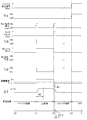
- FIG. 3 is a time chart schematically showing a time transition of each signal according to the embodiment.
- FIG. 1 is a schematic block diagram of a power supply control circuit 10 according to an embodiment of the present invention.
- FIG. 2 is a block diagram of the power supply control circuit 10 in more detail.
- FIG. 3 is a time chart showing a time transition of each signal according to an embodiment.
- the power supply control circuit 10 is connected to an energization path 51 that supplies power from the power source Ba to the load 50, and a semiconductor switch 30 that turns on / off power energization, and a semiconductor switch 30 And a control circuit 20 that controls the semiconductor switch 30 and the energization path 51.
- the power supply control circuit 10 is further a bypass circuit 40 arranged in parallel with the semiconductor switch 30, and when the load 50 is in a non-energized state or in a standby state when the control circuit 20 is not activated, the battery power supply A bypass circuit 40 for connecting Ba to the load 50 is provided.
- the bypass circuit 40 includes an energization determination circuit 41 that detects that the load 50 is in an operating state and generates an activation signal Wps that activates the control circuit 20 in response to the detection of the operating state of the load 50.
- the energization determination circuit 41 supplies the activation signal Wps to the control circuit 20, thereby turning on the semiconductor switch 30 and causing the load 50 to supply power from the power source Ba via the energization path 51.
- the power supply control circuit 10 is mounted on an automobile, the power source Ba is a battery, and the ECU as the load 50 is driven and controlled by the power supply control circuit 10 via an electric wire that is a current path 51. An example is shown.
- the control circuit 20 includes an FET drive circuit 21, a current detection / wire temperature calculation circuit 22, a Wake-up circuit 23, a latch reset circuit (an example of a “non-energization determination circuit”) 24, a transistor Tr5, and the like.
- the FET drive circuit 21 controls on / off of the main switch 31 of the semiconductor switch 30 and the transistor Tr5 in accordance with the state switching signal Mcs from the Wake-up circuit 23.
- the current detection / wire temperature calculation circuit 22 is connected to the sense transistor 32 of the semiconductor switch 30 to detect the current flow It of the load 50 and to determine the temperature of the current path (wire) 51 from the amount of the detected current flow It.
- the increase ⁇ T is calculated.
- the energization current It becomes equal to or less than the threshold value Ith, or after a predetermined time (see K2 in FIG. 3) when the temperature rise ⁇ T of the energization path (electric wire) 51 due to the load 50 being energized is saturated.
- a determination signal Jds for determining that the load 50 is in a non-energized state or a standby state is generated, and the determination signal Jds is supplied to the latch reset circuit 24.
- the Wake-up circuit 23 switches the state of the control circuit 20 from the standby state to the activated state according to the Wake-up signal (an example of “activation signal”) Wps from the bypass circuit 40.
- the Wake-up circuit 23 receives the Wake-up signal Wps, the Wake-up circuit 23 generates a state switching signal Mcs and supplies the state switching signal Mcs to the FET drive circuit 21, the current detection / wire temperature calculation circuit 22 and the latch reset circuit 24. .
- the latch reset circuit 24 When the latch reset circuit 24 receives the determination signal Jds or the load command signal Los that sets the load 50 in a non-energized state (off state) or a standby state, the latch reset circuit 24 determines that the load 50 is in a non-energized state or a standby state. The latch reset circuit 24 generates a latch reset signal Res and supplies the latch reset signal Res to the latch circuit 42 of the bypass circuit 40 in order to switch the control circuit 20 from the activated state to the standby state.
- the semiconductor switch 30 includes a main switch 31 that supplies power to the load 50 and a sense transistor 32 that detects an energization current It.
- the main switch 31 and the sense transistor 32 are configured by, for example, an N channel FET (field effect transistor).
- the bypass circuit 40 includes an energization determination circuit 41, a bypass prohibition circuit 43, a bypass path 45, a transistor Tr1 (an example of a “circuit cutoff element”), a transistor Tr2 (path cutoff element), a resistor R2, a capacitor C1, and the like.
- the bypass circuit 40 may not include the transistor Tr1 and the bypass prohibition circuit 43.
- the energization determination circuit 41 includes a latch circuit 42, a transistor Tr3, and a resistor R3.
- the transistor Tr3 is configured by, for example, a P-channel FET, the transistor Tr2 is turned on, and the path voltage in the bypass path 45 (see the position P1 in FIG. 2) is in the range of the on-voltage (corresponding to a “predetermined range value”). Turns on.
- the latch circuit 42 generates the Wake-up signal Wps as a latch signal by the potential generated at one end of the resistor R3, and supplies the Wake-up signal Wps to the Wake-up circuit 23 of the control circuit 20.
- the transistor Tr2 is composed of, for example, a P-channel FET, and is on / off controlled by the transistor Tr1 and the transistor Tr5 of the control circuit 20. When the transistor Tr2 is turned off, the bypass path 45 is blocked.
- the resistor R2 is provided to form a voltage (path voltage) that turns on the transistor Tr2 at the end P1 of the bypass path 45 when the transistor Tr2 is turned on.
- the resistor R2 has a resistance value that can limit the current It so that the current (energization current) It flowing through the energization path 51 is equal to or less than a current value that does not damage the energization path 51 when the load 50 is short-circuited. .
- the capacitor C1 is connected in parallel to the resistor R2 and smoothes the signal passing through the bypass path 45. That is, the capacitor C ⁇ b> 1 is provided in order to prevent malfunction of the latch circuit 42 due to pulse noise entering the bypass path 45.
- the capacitor C1 may be omitted.
- the bypass prohibition circuit 43 includes, for example, a transistor Tr4 and a resistor R4 configured by a P-channel FET.
- the bypass prohibition circuit 43 controls the transistor Tr1 according to the bypass prohibition signal Bhs (an example of a “predetermined instruction signal”), and shuts off the bypass circuit 40. For example, when an automobile is loaded for transportation, the operation of the bypass circuit 40 is interrupted by turning on the transistor Tr1 and turning off the transistor Tr2.
- the voltage drop due to the resistance R2 of the bypass circuit 40 increases as the bypass current Ib flowing through the bypass path 45 increases due to the state change of the ECU 5.
- the voltage drop reaches a predetermined value or more, that is, when the voltage drop reaches or exceeds the ON voltage of the transistor Tr3 of the energization determination circuit 41, the transistor Tr3 is turned ON.
- the transistor Tr3 is turned on, the terminal voltage of the resistor 3 of the energization determining circuit 41 increases, and the latch circuit 42 operates accordingly. That is, the latch circuit 42 validates the Wake-up signal Wps. For example, as shown in FIG. 3, the Wake-up signal Wps is changed from a low level to a high level.
- the Wake-up circuit 23 when the Wake-up circuit 23 receives the Wake-up signal Wps, the Wake-up circuit 23 generates a state switching signal Mcs and sends the state switching signal Mcs to the FET drive circuit 21, the current detection / wire temperature calculation circuit 22, and the latch reset circuit 24. Supply.
- the FET drive circuit 21 turns on the main switch 31 in response to the state switching signal Mcs, and immediately after that turns on the transistor Tr5 configured by, for example, a P-channel FET.
- the transistor Tr5 When the transistor Tr5 is turned on, the transistor Tr2 of the bypass circuit 40 is turned off, so that the bypass path 45 is blocked. That is, the energization path of the ECU 5 is switched from the bypass path 45 to the main path 35.
- the latch reset circuit 24 supplies the latch reset signal Res to the latch circuit 42 of the bypass circuit 40 to change the Wake-up signal Wps from, for example, a high level to a low level.
- the wake-up circuit 23 When the wake-up circuit 23 receives the invalidated wake-up signal Wps, the wake-up circuit 23 generates a state switching signal Mcs for switching the state of the control circuit 20 from the activated state to the standby state, and the state switching signal Mcs is converted into the FET drive circuit 21.
- the current detection / wire temperature calculation circuit 22 and the latch reset circuit 24 are supplied.
- the FET drive circuit 21 turns off the main switch 31 and immediately turns off the transistor Tr5 in response to the state switching signal Mcs.
- the transistor Tr5 When the transistor Tr5 is turned off, the transistor Tr2 of the bypass circuit 40 is turned on, so that the bypass path 45 is brought into a normal state. That is, the energization path of the ECU 5 is switched from the main path 35 to the bypass path 45.
- a high-level bypass prohibition signal Bhs is prohibited from bypassing.
- the signal is supplied to the gate of the transistor Tr4 of the circuit 43.
- the gate of the transistor Tr4 is pulled up.
- the bypass path 45 is blocked.
- the main path 35 is also blocked, the energization path to the ECU 50 is completely turned off.
- the bypass circuit 40 connects the battery Ba and the ECU 50 via the bypass path 45 when the ECU (load) 50 is in a standby state in a non-activated state of the control circuit 20, for example, in a standby state. Electric power is supplied to the ECU 50. Then, when the ECU 50 is in an operating state, the semiconductor switch 30 is turned on, electric power is supplied to the ECU 50 via the main path 35, and the bypass path 45 is blocked. Therefore, the power consumption by the control circuit 20 and the semiconductor switch 30 when the ECU 50 is in the standby state can be significantly reduced only to the standby power of the control circuit 20.
- bypass path 45 can be blocked by the bypass prohibition circuit 43. Therefore, when the ECU 50 is completely turned off, for example, when the automobile is loaded for transportation, the power consumed via the bypass circuit 40 can be reduced.
- the latch reset circuit (non-energization determination circuit) 24 determines that the ECU (load) 50 is in the standby state
- the semiconductor switch 30 is turned off and the control circuit 20 itself is not activated.
- the example in which it is determined that the ECU (load) 50 is in a non-energized state based on the load command signal Los is shown, but the present invention is not limited thereto.
- the latch reset circuit 24 may determine that the ECU 50 is in a non-energized state when the energized current It is equal to or less than the threshold current Ith.
- the non-energized state of the ECU 50 may be determined based on the fact that the state where the energized current It is equal to or less than the threshold current Ith continues for a predetermined period K1 (see time t2-1 in FIG. 3).
- the latch reset circuit 24 increases the temperature of the energization path 51 after a predetermined time (see K ⁇ b> 2 in FIG. 3) when the temperature increase of the energization path 51 is saturated when the ECU 50 is energized.
- the non-energized state of the ECU 50 may be determined (see time t2-2 in FIG. 3).
- the latch reset circuit (non-energization determining circuit) 24 determines that the ECU (load) 50 is in the non-energized state, the semiconductor switch 30 is turned off and the control circuit 20 itself is not activated.
- the example in which the latch reset signal Res is generated and performed via the bypass circuit 40 is shown, but the present invention is not limited thereto.
- the latch reset circuit 24 may directly turn off the semiconductor switch 30 and the transistor Tr5 without going through the bypass circuit 40, so that the control circuit 20 itself is in a non-activated state.
- the configuration of the energization determination circuit 41 is not limited to that shown in FIG.
- the energization determination circuit 41 may be basically configured to generate an activation signal that activates the control circuit 20 in response to the load being in an operating state.
- the transistor Tr3 may be configured by an N-channel FET. In that case, a voltage between the resistor R2 and the transistor Tr2 may be applied to the gate of the transistor Tr3.
- the load is an ECU and the ECU saves power in the power supply control circuit 10 in a standby state.
- the present invention omits the power supply control circuit 10 in a non-energized state. It can also be applied to power generation.
Landscapes
- Business, Economics & Management (AREA)
- Emergency Management (AREA)
- Engineering & Computer Science (AREA)
- Power Engineering (AREA)
- Electronic Switches (AREA)
- Direct Current Feeding And Distribution (AREA)
Abstract
Description
ところで、電源供給が必要な負荷の上流に半導体ヒューズとして半導体スイッチ素子を使用する場合において、負荷によっては、その非通電状態、または、待機状態においても、電源から負荷への電圧印加、あるいは電力供給が要求される場合ある。例えば、負荷が車に搭載されるECU(エンジンコントロールユニット)である場合、ECUを待機状態に維持するために、半導体スイッチ素子への駆動電流およびその制御回路への電力供給が必要となる。その場合、負荷の非通電状態、あるいは待機状態においても電力供給制御回路において所定の電力が消費されている。そのため、負荷の非通電状態、または、待機状態における電力供給制御回路の省電力化が所望されている。
本発明は上記のような事情に基づいて完成されたものであって、本発明に係る電力供給制御回路は、電源から負荷へ電力を供給する通電路に接続され、前記電力の通電をオン・オフする半導体スイッチと、前記半導体スイッチのオン・オフを制御するとともに、前記半導体スイッチおよび前記通電路の保護を行う制御回路とを有する電力供給制御回路において、前記半導体スイッチに並列配置されるバイパス回路であって、前記制御回路の非起動状態において、前記負荷が非通電状態、または、待機状態の場合に、前記電源を前記負荷に接続するバイパス回路を備え、前記バイパス回路は、前記負荷が動作状態とされることに応じて前記制御回路を起動させる起動信号を生成する通電判定回路であって、前記起動信号を前記制御回路に供給することによって、前記半導体スイッチをオンさせ、前記通電路を介して前記負荷に電力を供給させる、通電判定回路を有する、ことを特徴とする。
20...制御回路
22...電流検出・電線温度演算回路(電流検出回路、温度演算回路、非通電検出回路)
24...ラッチリセット回路(非通電検出回路)
30...半導体スイッチ
31...メインスイッチ
40...バイパス回路
41...通電判定回路
42...ラッチ回路
43...バイパス禁止回路
45...バイパス経路
50...ECU(負荷)
51...電線(通電路)
C1...コンデンサ
Los...負荷指令信号(指令信号)
Tr1...トランジスタ(回路遮断素子)
Tr2...トランジスタ(経路遮断素子)
It...通電電流
R2...抵抗
Wp...ウェイク・アップ信号(起動信号)
本発明の一実施形態について図1~図3を参照しつつ説明する。図1は、本発明の一実施形態に係る電力供給制御回路10の概略的なブロック図である。図2は、より詳細な電力供給制御回路10のブロック図である。図3は、一実施形態に係る各信号の時間推移を示すタイムチャートである。
電力供給制御回路10は、図1に示されるように、電源Baから負荷50へ電力を供給する通電路51に接続され、電力の通電をオン・オフする半導体スイッチ30と、半導体スイッチ30のオン・オフを制御するとともに、半導体スイッチ30および通電路51の保護を行う制御回路20とを含む。電力供給制御回路10は、さらに、半導体スイッチ30に並列配置されるバイパス回路40であって、制御回路20の非起動状態において、負荷50が非通電状態、または、待機状態の場合に、バッテリー電源Baを負荷50に接続するバイパス回路40を備える。
次に、図3のタイムチャートを参照して、本実施形態における電力供給制御回路10の動作を説明する。
今、制御回路20および負荷(ECU)50が待機状態であって、ECU50にはバイパス経路45から電力が供給されている状態にあるとする(図3の時刻t0~t1参照)。この状態において、図3の時刻t1に、負荷(ECU)50を待機状態から通電状態(動作状態)とするために、例えば、リモコン装置から負荷指令信号LosがECU5に供給されたとする。
バイパス回路40は、制御回路20の非起動状態、例えば、待機状態において、ECU(負荷)50が待機状態の場合に、バッテリーBaとECU50とを、バイパス経路45を介して接続し、バッテリーBaの電力をECU50に供給する。そして、ECU50が動作状態とされると、半導体スイッチ30がオンされ主経路35を介してECU50に電力が供給されるとともに、バイパス経路45が遮断される。そのため、ECU50が待機状態おける、制御回路20および半導体スイッチ30による消費電力を、単に制御回路20の待機電力のみに大幅に低減することができる。
本発明は上記記述及び図面によって説明した実施形態に限定されるものではなく、例えば次のような実施形態も本発明の技術的範囲に含まれる。
Claims (11)
- 電源から負荷へ電力を供給する通電路に接続され、前記電力の通電をオン・オフする半導体スイッチと、前記半導体スイッチのオン・オフを制御するとともに、前記半導体スイッチおよび前記通電路の保護を行う制御回路とを有する電力供給制御回路において、
前記半導体スイッチに並列配置されるバイパス回路であって、前記制御回路の非起動状態において、前記負荷が非通電状態、または、待機状態の場合に、前記電源を前記負荷に接続するバイパス回路を備え、
前記バイパス回路は、
前記負荷が動作状態とされることに応じて前記制御回路を起動させる起動信号を生成する通電判定回路であって、前記起動信号を前記制御回路に供給することによって、前記半導体スイッチをオンさせ、前記通電路を介して前記負荷に電力を供給させる、通電判定回路を有する、ことを特徴とする電力供給制御回路。 - 前記バイパス回路は、
前記電源と前記負荷との間に設けられるバイパス経路を有し、
前記通電判定回路は、前記バイパス経路内において形成される経路電圧が所定範囲の値となる場合に前記起動信号を生成する、請求の範囲第1項に記載の電力供給制御回路。 - 前記バイパス経路は抵抗を含み、
前記経路電圧は、前記抵抗によって形成される、請求の範囲第2項に記載の電力供給制御回路。 - 前記バイパス経路は、前記抵抗に並列接続されたコンデンサをさらに含む請求の範囲第3項に記載の電力供給制御回路。
- 前記抵抗は、前記負荷がショートした場合に前記通電路に流れる電流が該通電路を損傷しない電流値以下となるように、前記電流を制限可能な抵抗値を有する、請求の範囲第3項または第4項に記載の電力供給制御回路。
- 前記バイパス回路は、前記バイパス経路を遮断する経路遮断素子を有し、
前記制御回路は、
前記半導体スイッチに流れる電流に応じて、前記半導体スイッチおよび前記通電路の保護を行い、
前記起動信号によって起動すると、前記半導体スイッチをオンした後、前記経路遮断素子を制御して前記バイパス経路を遮断する、請求の範囲第2項から第5項のいずれか一項に記載の電力供給制御回路。 - 前記バイパス回路は、
前記バイパス回路を遮断する回路遮断素子と、
所定の指示信号に応じて前記回路遮断素子を制御して、前記バイパス回路を遮断するバイパス禁止回路とをさらに有する、請求の範囲第2項から第6項のいずれか一項に記載の電力供給制御回路。 - 前記制御回路は、
前記負荷が非通電状態、または待機状態であることを判定すると、前記半導体スイッチをオフし、該制御回路自身を非起動状態とする非通電判定回路を有する、請求の範囲第1項から第7項のいずれか一項に記載の電力供給制御回路。 - 前記非通電判定回路は、前記負荷を非通電状態、または待機状態とする負荷指令信号によって、前記負荷の非通電状態または待機状態を判定する、請求の範囲第8項に記載の電力供給制御回路。
- 前記制御回路は、前記負荷の通電電流を検出する電流検出回路を有し、
前記非通電判定回路は、検出された前記通電電流がしきい値電流以下であることにより、前記負荷の非通電状態または待機状態を判定する、請求の範囲第8項に記載の電力供給制御回路。 - 前記制御回路は、前記負荷に通電される電流量から前記通電路の温度上昇を演算する温度演算回路を有し、
前記非通電判定回路は、前記負荷が通電されることによる前記通電路の温度上昇が飽和する所定時間以降において、前記通電路の温度上昇演算値がしきい値以下であることにより、前記負荷の非通電状態または待機状態を判定する、請求の範囲第8項に記載の電力供給制御回路。
Priority Applications (3)
| Application Number | Priority Date | Filing Date | Title |
|---|---|---|---|
| CN201080003576.3A CN102246375B (zh) | 2009-01-30 | 2010-01-29 | 电力供给控制电路 |
| DE112010000432.3T DE112010000432B4 (de) | 2009-01-30 | 2010-01-29 | Elektrische Energieversorgungssteuerschaltung |
| US13/123,389 US8754551B2 (en) | 2009-01-30 | 2010-01-29 | Electric power supply control circuit |
Applications Claiming Priority (2)
| Application Number | Priority Date | Filing Date | Title |
|---|---|---|---|
| JP2009-020513 | 2009-01-30 | ||
| JP2009020513A JP5413642B2 (ja) | 2009-01-30 | 2009-01-30 | 電力供給制御回路 |
Publications (1)
| Publication Number | Publication Date |
|---|---|
| WO2010087426A1 true WO2010087426A1 (ja) | 2010-08-05 |
Family
ID=42395680
Family Applications (1)
| Application Number | Title | Priority Date | Filing Date |
|---|---|---|---|
| PCT/JP2010/051195 Ceased WO2010087426A1 (ja) | 2009-01-30 | 2010-01-29 | 電力供給制御回路 |
Country Status (5)
| Country | Link |
|---|---|
| US (1) | US8754551B2 (ja) |
| JP (1) | JP5413642B2 (ja) |
| CN (1) | CN102246375B (ja) |
| DE (1) | DE112010000432B4 (ja) |
| WO (1) | WO2010087426A1 (ja) |
Families Citing this family (8)
| Publication number | Priority date | Publication date | Assignee | Title |
|---|---|---|---|---|
| US9046555B2 (en) * | 2011-12-19 | 2015-06-02 | Tyco Safety Products Canada Ltd. | Latching over-current protection circuit and method |
| JP5605856B2 (ja) | 2012-02-20 | 2014-10-15 | オムロンオートモーティブエレクトロニクス株式会社 | 電源制御装置 |
| KR101882800B1 (ko) | 2012-02-28 | 2018-08-01 | 삼성전자주식회사 | 무선 전력 수신기 및 그 제어 방법 |
| JP6260552B2 (ja) * | 2015-02-26 | 2018-01-17 | 株式会社オートネットワーク技術研究所 | 電力供給装置 |
| JP7156047B2 (ja) * | 2019-01-16 | 2022-10-19 | 株式会社島津製作所 | クロマトグラフ装置およびロードスイッチ回路 |
| EP3787139A1 (en) * | 2019-08-29 | 2021-03-03 | Aptiv Technologies Limited | Electrical safety system for providing overcurrent protection of an electrical circuit in a vehicle |
| CN113050500A (zh) * | 2021-03-24 | 2021-06-29 | 北京星际荣耀空间科技股份有限公司 | 箭上供电控制系统、箭上供电系统的控制方法及装置 |
| DE102024117378A1 (de) * | 2024-06-20 | 2025-12-24 | HELLA GmbH & Co. KGaA | Elektronische Sicherungseinrichtung |
Citations (3)
| Publication number | Priority date | Publication date | Assignee | Title |
|---|---|---|---|---|
| JPH1185293A (ja) * | 1997-09-08 | 1999-03-30 | Fujitsu Ten Ltd | 電圧制御回路 |
| JP2002341978A (ja) * | 2001-05-11 | 2002-11-29 | Furukawa Electric Co Ltd:The | 電子制御装置 |
| JP2007312543A (ja) * | 2006-05-19 | 2007-11-29 | Auto Network Gijutsu Kenkyusho:Kk | 電源モジュール |
Family Cites Families (9)
| Publication number | Priority date | Publication date | Assignee | Title |
|---|---|---|---|---|
| DE19941699A1 (de) | 1999-09-02 | 2001-03-08 | Bosch Gmbh Robert | Halbleitersicherung für elektrische Verbraucher |
| JP2001217696A (ja) | 2000-02-04 | 2001-08-10 | Auto Network Gijutsu Kenkyusho:Kk | 過電流検出回路 |
| JP2003048497A (ja) * | 2001-08-07 | 2003-02-18 | Yazaki Corp | 電力分配システム |
| JP3925411B2 (ja) * | 2003-01-10 | 2007-06-06 | 享久 笠茂 | 電力管理システム及び電力計測装置 |
| JP2005312162A (ja) * | 2004-04-20 | 2005-11-04 | Fujitsu Ltd | 電子機器における省電力制御方法および装置並びに省電力型電子機器 |
| JP2006058013A (ja) * | 2004-08-17 | 2006-03-02 | Sony Corp | 電気機器 |
| JP2006115622A (ja) * | 2004-10-15 | 2006-04-27 | Hanshin Electric Co Ltd | 使用電力監視方法および使用電力監視システム |
| JP2007020260A (ja) * | 2005-07-06 | 2007-01-25 | Matsushita Electric Ind Co Ltd | 電力供給システムならびに電力供給サービス方法 |
| JP4802046B2 (ja) * | 2006-06-14 | 2011-10-26 | トヨタホーム株式会社 | 建物の電力監視システム |
-
2009
- 2009-01-30 JP JP2009020513A patent/JP5413642B2/ja active Active
-
2010
- 2010-01-29 WO PCT/JP2010/051195 patent/WO2010087426A1/ja not_active Ceased
- 2010-01-29 DE DE112010000432.3T patent/DE112010000432B4/de active Active
- 2010-01-29 CN CN201080003576.3A patent/CN102246375B/zh active Active
- 2010-01-29 US US13/123,389 patent/US8754551B2/en active Active
Patent Citations (3)
| Publication number | Priority date | Publication date | Assignee | Title |
|---|---|---|---|---|
| JPH1185293A (ja) * | 1997-09-08 | 1999-03-30 | Fujitsu Ten Ltd | 電圧制御回路 |
| JP2002341978A (ja) * | 2001-05-11 | 2002-11-29 | Furukawa Electric Co Ltd:The | 電子制御装置 |
| JP2007312543A (ja) * | 2006-05-19 | 2007-11-29 | Auto Network Gijutsu Kenkyusho:Kk | 電源モジュール |
Also Published As
| Publication number | Publication date |
|---|---|
| CN102246375A (zh) | 2011-11-16 |
| JP5413642B2 (ja) | 2014-02-12 |
| CN102246375B (zh) | 2014-06-25 |
| US8754551B2 (en) | 2014-06-17 |
| DE112010000432B4 (de) | 2017-11-16 |
| DE112010000432T5 (de) | 2013-04-25 |
| US20110193414A1 (en) | 2011-08-11 |
| JP2010178558A (ja) | 2010-08-12 |
Similar Documents
| Publication | Publication Date | Title |
|---|---|---|
| JP5413642B2 (ja) | 電力供給制御回路 | |
| JP5162335B2 (ja) | リレー制御装置 | |
| US9197127B2 (en) | Power supply controller | |
| US8918222B2 (en) | Controlling and protecting power-supply paths from thermal overloads | |
| JP4359855B2 (ja) | 電磁弁駆動回路及び電磁弁 | |
| JP4180597B2 (ja) | 給電回路の異常検出装置 | |
| JP2007174490A5 (ja) | ||
| JP2010110091A (ja) | 負荷駆動装置 | |
| JP2012143110A (ja) | 突入電流防止回路及び電源供給制御装置 | |
| JP2010104079A (ja) | 負荷駆動装置 | |
| JP6030849B2 (ja) | 半導体スイッチの制御装置 | |
| KR101522998B1 (ko) | 전원 절환 장치 | |
| US20140362478A1 (en) | Power system and short-circuit protection circuit thereof | |
| KR101952098B1 (ko) | 전동식 부스터 시스템의 전원 안정화 장치 및 그 방법 | |
| WO2015037441A1 (ja) | 制御システム | |
| JP2010110092A (ja) | 駆動装置 | |
| JP2011041349A (ja) | 負荷回路の制御装置 | |
| JP6882023B2 (ja) | 電線保護装置 | |
| JP5423482B2 (ja) | 半導体式ラッチリレー | |
| JP2012222600A (ja) | 電子制御装置 | |
| JP2005150920A (ja) | 出力回路 | |
| JP5174946B1 (ja) | コイル駆動装置 | |
| JP2011205865A (ja) | 電源供給装置及び電源供給方法 | |
| JP2007068286A (ja) | 誘導性ロード制御装置 | |
| KR20070076174A (ko) | 모터 구동회로 |
Legal Events
| Date | Code | Title | Description |
|---|---|---|---|
| WWE | Wipo information: entry into national phase |
Ref document number: 201080003576.3 Country of ref document: CN |
|
| 121 | Ep: the epo has been informed by wipo that ep was designated in this application |
Ref document number: 10735888 Country of ref document: EP Kind code of ref document: A1 |
|
| WWE | Wipo information: entry into national phase |
Ref document number: 13123389 Country of ref document: US |
|
| NENP | Non-entry into the national phase |
Ref country code: DE |
|
| 122 | Ep: pct application non-entry in european phase |
Ref document number: 10735888 Country of ref document: EP Kind code of ref document: A1 |