WO2010079639A1 - 半導体発光装置およびその製造方法 - Google Patents
半導体発光装置およびその製造方法 Download PDFInfo
- Publication number
- WO2010079639A1 WO2010079639A1 PCT/JP2009/065756 JP2009065756W WO2010079639A1 WO 2010079639 A1 WO2010079639 A1 WO 2010079639A1 JP 2009065756 W JP2009065756 W JP 2009065756W WO 2010079639 A1 WO2010079639 A1 WO 2010079639A1
- Authority
- WO
- WIPO (PCT)
- Prior art keywords
- electrode
- emitting device
- light emitting
- semiconductor light
- manufacturing
- Prior art date
- Legal status (The legal status is an assumption and is not a legal conclusion. Google has not performed a legal analysis and makes no representation as to the accuracy of the status listed.)
- Ceased
Links
Images


Classifications
-
- H—ELECTRICITY
- H10—SEMICONDUCTOR DEVICES; ELECTRIC SOLID-STATE DEVICES NOT OTHERWISE PROVIDED FOR
- H10H—INORGANIC LIGHT-EMITTING SEMICONDUCTOR DEVICES HAVING POTENTIAL BARRIERS
- H10H20/00—Individual inorganic light-emitting semiconductor devices having potential barriers, e.g. light-emitting diodes [LED]
- H10H20/80—Constructional details
- H10H20/81—Bodies
- H10H20/819—Bodies characterised by their shape, e.g. curved or truncated substrates
- H10H20/82—Roughened surfaces, e.g. at the interface between epitaxial layers
-
- H—ELECTRICITY
- H10—SEMICONDUCTOR DEVICES; ELECTRIC SOLID-STATE DEVICES NOT OTHERWISE PROVIDED FOR
- H10H—INORGANIC LIGHT-EMITTING SEMICONDUCTOR DEVICES HAVING POTENTIAL BARRIERS
- H10H20/00—Individual inorganic light-emitting semiconductor devices having potential barriers, e.g. light-emitting diodes [LED]
- H10H20/01—Manufacture or treatment
Definitions
- the present invention relates to a method for manufacturing a semiconductor light emitting device in which an improved concavo-convex structure is formed on a light extraction surface, and a semiconductor light emitting device manufactured by the method.
- the formation of the concavo-convex structure is usually performed after an electrode is formed on the light extraction surface. After a self-assembled film is formed on the light extraction surface by spin coating, a concavo-convex structure is formed on the light extraction surface by dry etching using the self-organization pattern as a mask.
- the thickness of the electrode is usually 1 ⁇ m or more, when the self-assembled film is formed by spin coating, the step in the vicinity of the electrode is large, so that the self-assembled film is formed larger than the target film thickness. Therefore, the portion near the thick electrode cannot transfer the self-organized pattern to the light extraction surface.
- the area where the concavo-convex structure is formed is reduced, and there is room for improvement with respect to the luminance of the light-emitting device because the concavo-convex structure is difficult to be formed in the vicinity of an electrode having particularly strong light emission.
- Patent Document 2 describes a method of forming an uneven structure on the light extraction surface using photolithography and finally forming an electrode. Although this method can form a concavo-convex structure in a region relatively close to the electrode, it cannot form a good concavo-convex structure when a semiconductor having a high etching rate such as GaAs is included.
- the present invention provides a method for manufacturing a semiconductor light emitting device, in which an electrode and an uneven structure can be formed closer to each other on the light extraction surface of the semiconductor light emitting device.
- a method of manufacturing a semiconductor light emitting device includes: A method of manufacturing a semiconductor light emitting device in which an electrode and a concavo-convex structure are formed on a surface of a semiconductor layer from which light is extracted, Laminating an active layer and the semiconductor layer on a substrate; Forming a contact layer on the semiconductor layer for generating an ohmic contact between the surface of the semiconductor layer and the electrode; Forming an oxide film on the surface of the semiconductor layer where the electrode is to be formed; Forming a protective film on the entire surface of the semiconductor layer including the oxide film; Forming a self-assembled film on the protective film; Processing the protective film by dry etching using the self-assembled film as a mask to form a protective film mask; Processing the semiconductor layer by dry etching using the protective film mask to form a concavo-convex structure; Removing the portion of the protective film that forms the electrode and depositing a conductive material on the contact layer to form an electrode; It is characterized by having.
- a method of manufacturing a semiconductor light emitting device includes: A method of manufacturing a semiconductor light emitting device in which an electrode and a concavo-convex structure are formed on a surface of a semiconductor layer from which light is extracted, Laminating an active layer and the semiconductor layer on a substrate; Forming an oxide film on the surface of the semiconductor layer where the electrode is to be formed; Forming a protective film on the entire surface of the semiconductor layer including the oxide film; Forming a self-assembled film on the protective film; Processing the protective film by dry etching using the self-assembled film as a mask to form a protective film mask; Processing the semiconductor layer by dry etching using the protective film mask to form a concavo-convex structure; Removing the protective film in the portion where the electrode is to be formed, and depositing a conductive material on the contact layer to form an electrode; And a step of generating an ohmic contact between the surface of the semiconductor layer and the electrode.
- a semiconductor light emitting device is manufactured by any one of the above manufacturing methods.
- a semiconductor light-emitting device is a semiconductor light-emitting device in which an electrode and a concavo-convex structure are formed on the surface of a semiconductor layer from which light is extracted, and the region is within 10 ⁇ m from the electrode. An uneven structure is formed.
- the present invention it is possible to form a concavo-convex structure in a region closer to the electrode by first protecting the electrode forming portion and finally forming the electrode. As a result, the area where the uneven structure is not formed is reduced, and the uneven structure can be formed in the vicinity of the electrode from which stronger light emission can be extracted, so that the luminance improvement rate is improved.
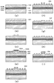
- Sectional drawing showing the structure of LED manufactured by the method concerning one Embodiment of this invention is a schematic cross-sectional view showing a method for manufacturing a semiconductor light emitting device according to an embodiment of the present invention.
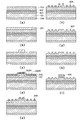
- 9 is a schematic cross-sectional view showing a method for manufacturing the semiconductor light emitting device of Example 2.
- FIG. 10 is a schematic cross-sectional view showing a method for manufacturing the semiconductor light emitting device of Example 3.
- FIG. 1 is a cross-sectional view showing the structure of an LED manufactured by the method according to an embodiment of the present invention.
- the light emitting device shown in this figure includes a substrate 101 made of, for example, n-type GaAs.
- a heterostructure portion 102 including, for example, an n-type InAlP cladding layer, an InGaP active layer, a p-type InAlP cladding layer, and the like is formed on the substrate 101, and a current diffusion layer 103 made of, for example, p-type InGaAlP is formed thereon.
- a p-side electrode 105 is formed on a part of the current diffusion layer 103.
- a thin GaAs contact layer 104 for making ohmic contact is formed between the electrode 105 and the current diffusion layer 103.
- the current diffusion layer 103 is a multi-element layer, for example, a layer made of a ternary or higher element such as InGaAlP or AlGaAs, it is formed on the contact layer without such a contact layer. It becomes difficult for the electrode to make ohmic contact. If an ohmic contact cannot be obtained, current loss occurs and light emission decreases. Therefore, this contact layer is necessary.
- the material used as the material of the contact layer varies depending on the types of semiconductor layers and electrodes adjacent to both sides of the contact layer, but GaAs or GaP is generally preferable.
- An n-side electrode 106 is formed on the back side of the substrate. Light emitted from the active layer is extracted from the surface of the current diffusion layer 103 where the electrode 105 is not formed.
- a minute protrusion 107 is formed on the exposed surface where the electrode of the current diffusion layer is not formed, thereby forming a concavo-convex structure.
- a concavo-convex structure contributes to the improvement of the luminance of the LED.
- the concavo-convex structure cannot be formed in the vicinity of the electrode by the conventional manufacturing method.
- the interval (A) between the electrode in FIG. 1 and the protrusion forming the concavo-convex structure is generally 10 ⁇ m or more. This is because spin coating is used when forming a self-assembled film containing a block copolymer, and if the electrode is formed in advance, the self-assembled film becomes thick in the vicinity of the electrode, resulting in a step. is there.
- the distance between the electrode and the projection forming the concavo-convex structure can be made 10 ⁇ m or less, and a light emitting device in which the region where the concavo-convex structure is formed is enlarged is manufactured. Became possible.
- the distance between the electrode and the protrusion forming the concavo-convex structure can be remarkably shortened. However, if the distance is generally less than 1 ⁇ m, the current spread in the current diffusion layer is deteriorated, and the activity is reduced. Since the light emitting region in the layer becomes narrow, it is not preferable in that the internal luminous efficiency is lowered.
- a heterostructure portion 102 including an n-type InAlP cladding layer, an InGaP active layer, a p-type InAlP cladding layer, etc. is formed on an n-GaAs substrate 101, and a p-type InGaAlP current diffusion layer 103 is epitaxially grown thereon.
- a p-type GaAs contact layer 104 (0.1 ⁇ m) is formed on the current diffusion layer in order to make an ohmic contact.
- the n-side electrode 106 is formed on the back side of the substrate (FIG. 2A).
- a SiO 2 film 201 is formed on the entire surface of the light emitting element substrate by chemical vapor deposition (hereinafter referred to as CVD) (FIG. 2B).
- CVD chemical vapor deposition
- a resist film (not shown) is formed on the SiO 2 film 201, and a resist pattern for electrode formation is formed by performing exposure and development.
- the SiO 2 film is processed by wet etching using the resist pattern.
- the GaAs contact layer is processed by wet etching.
- the remaining resist film is removed (FIG. 2C).
- the GaAs contact layer is removed leaving a portion where an electrode is formed.
- a protective film for forming a concavo-convex structure on the substrate surface for example, a SiO 2 film 202 is formed.
- the thickness of the protective film is 300 nm or less, the thick film portion in the vicinity of the electrode after the application of a self-assembled film, which will be described later, can be greatly reduced, and the region where the concavo-convex structure is formed is preferable.
- a solution obtained by dissolving a block copolymer, which is a microphase separation structure composition, in a solvent is applied onto the SiO 2 film by spin coating to form a block copolymer film 203, and then prebaked to remove the solvent in the film. .
- a block copolymer having a polystyrene segment and a polymethyl methacrylate segment can be used.
- annealing is performed in a nitrogen atmosphere, and the phase separation of the block copolymer is performed (FIG. 2D).
- a plurality of polymer fragments (203A, 203B) constituting the block copolymer are formed.
- the block copolymer film is etched by reactive ion etching (hereinafter referred to as RIE) under the flow of an etching gas on the phase-separated substrate with the block copolymer film shown in FIG.
- RIE reactive ion etching
- the SiO 2 film is subjected to RIE processing using the polymer pattern 204 as a mask.
- the gas used is a fluorine-based gas such as CF 4 , CHF 3 , or C 4 F 8 , and Ar or O 2 may be added to the fluorine-based gas. Since the polymer mask 204 is unnecessary after RIE processing, it is generally removed by oxygen ashing or the like. By such an operation, the pattern 205 of the protective film (SiO 2 ) is formed (FIG. 2F).
- minute protrusions 107 are formed on the surface of the current diffusion layer of InGaAlP, and a minute uneven pattern is formed.
- the gas used for the RIE process is not limited to Cl 2, and etching can be performed even if BCl 3 , N 3 , or Ar is added.
- a concavo-convex pattern including, for example, a columnar protrusion 107 is formed on the surface of the issuing device (FIG. 2G).
- the upper and lower portions of the minute protrusion 107 are sputter-etched to form a conical shape, a cylindrical shape, and a truncated cone. An uneven structure having a shape is obtained.
- an inert gas for example, Ar gas or He gas
- the SiO 2 film protecting the electrode forming portion is removed by wet etching. Thereafter, a resist film for lift-off is formed, and a pattern for electrode formation is formed by development and exposure. Subsequently, the electrode 206 is formed by evaporating gold, for example. Thereafter, the resist is peeled off to form electrodes (FIG. 2 (i)). In this manner, a semiconductor light emitting device can be manufactured by the method of the present invention.
- SiO 2 film is used as the protective film of the electrode.
- those used as the protective film is not limited to SiO 2, it can be used other SiN, SiON, TiO 2 film, or the like.
- the present invention will be described in detail with reference to examples.
- the brightness of the LED in which the concavo-convex structure was formed after the conventional electrode was formed and the LED in which the concavo-convex structure was formed by the manufacturing method of the present invention were compared.
- Example 1 An LED was manufactured according to the method described above. As shown in FIG. 2A, a heterostructure portion 102 including an n-type InAlP clad layer, an InGaP active layer, a p-type InAlP clad layer, etc. was formed on an n-GaAs substrate 101. A current diffusion layer 103 containing a quaternary element of p-type InGaAlP is epitaxially grown thereon. A p-type GaAs contact layer 104 (0.1 ⁇ m) was formed on the current diffusion layer 103 in order to make an ohmic contact. An n-side electrode 106 was formed on the back side of the substrate. The emission wavelength of this LED was 635 nm.
- a SiO 2 film 201 was formed to a thickness of 300 nm on the entire surface of the light emitting element substrate by a CVD method (FIG. 2B). Thereafter, an i-line resist (THMR (trade name), manufactured by Tokyo Ohka Kogyo Co., Ltd.) was formed on the SiO 2 film with a thickness of 1 ⁇ m, and exposure and development were performed to form a resist pattern for electrode formation. .
- the SiO 2 film was wet etched with ammonium fluoride using the resist pattern.
- the GaAs contact layer 104 was wet etched with phosphoric acid. Finally, the resist was removed with a stripping solution (FIG. 2 (c)).
- a SiO 2 film 202 for forming a concavo-convex structure on the substrate surface was formed with a thickness of 100 nm by a CVD method.
- a solution obtained by dissolving a block copolymer having a polystyrene (hereinafter referred to as PS) block having a molecular weight of 315,000 and a polymethyl methacrylate (hereinafter referred to as PMMA) block having a molecular weight of 785,000 on SiO 2 in a solvent is spin-coated.
- PS polystyrene
- PMMA polymethyl methacrylate
- a block copolymer film 203 having a thickness of 150 nm.
- the film was annealed in a nitrogen atmosphere at 210 ° C. for 4 hours, phase separation between PS and PMMA was performed, and a PS dot pattern with a diameter of about 110 nm was formed (FIG. 2D).
- phase-separated block copolymer film was etched by performing RIE on the substrate with the phase-separated block copolymer under the conditions of an O 2 flow rate of 30 sccm, a pressure of 13.3 Pa (100 mTorr), and a power of 100 W.
- the PMMA is selectively etched due to the difference in the etching rate between PS and PMMA, and the PS pattern 204 remains as shown in FIG.
- the SiO 2 film 202 was etched under the conditions of a CF 4 flow rate of 30 sccm, a pressure of 1.33 Pa (10 mTorr), and a power of 100 W. Since the remaining PS pattern 204 is unnecessary, it was removed by O 2 ashing. As a result, a SiO 2 mask pattern was formed as shown in FIG.
- the SiO 2 film 201 protecting the electrode forming portion was removed by wet etching. Thereafter, a resist for lift-off (TLOR (trade name), manufactured by Tokyo Ohka Kogyo Co., Ltd.) was applied at a thickness of 3 ⁇ m to form a resist film, and a pattern for electrode formation was formed by performing development and exposure. . Subsequently, gold / gold-zinc was formed to a thickness of 1 ⁇ m by vapor deposition. Thereafter, the gold electrode 206 was formed by peeling the resist film with a stripping solution (FIG. 2 (i)). Finally, annealing was performed in a nitrogen atmosphere at 400 ° C. for 30 minutes in order to form ohmic properties between the electrode 206 and the GaAs contact layer 104. A semiconductor light emitting device (LED) according to the present invention was manufactured by such a method.
- TOR trade name
- gold / gold-zinc was formed to a thickness of 1 ⁇ m by vapor deposition.
- Example 1 Comparative Example 1 Next, for comparison, an LED having an uneven structure was manufactured by a conventional process. Specifically, a light-emitting element substrate on which gold electrodes were formed in advance was prepared for Example 1, and an uneven structure was formed thereon. The process for forming the concavo-convex structure was performed in the same manner as in Example 1.
- the concavo-convex structure was formed only from the region 12 ⁇ m away from the electrode, but in the LED of Example 1, the concavo-convex structure was formed from the region 1 to 5 ⁇ m away from the electrode. did it. Thereby, the LED of Example 1 showed a 20% improvement in luminance improvement over the LED of Comparative Example 1.
- Example 2 As shown in FIG. 3A, a double heterostructure 102 in which an InGaAlP active layer 102A is sandwiched between an n-InAlP clad layer 102B and a p-InAlP clad layer 102C is formed on an n-GaP substrate 101. Then, a p-GaP current diffusion layer 103 was formed. In this case, the p-GaP current diffusion layer is a semiconductor layer for extracting light, but can also be said to function as a contact layer. An n-side electrode 106 is formed on the entire opposite side surface of the n-GaP substrate, thereby forming an LED having an emission wavelength of 612 nm.
- a SiO 2 film 201 having a thickness of 200 nm was formed on the entire surface of the light emitting element substrate by a CVD method (FIG. 3B).
- an i-line resist (THMR (trade name), manufactured by Tokyo Ohka Kogyo Co., Ltd.) is applied onto the SiO 2 film to form a resist film with a thickness of 1 ⁇ m, and exposure and development are performed to form a resist for electrodes.
- a pattern was formed.
- the SiO 2 film was wet etched with ammonium fluoride using the resist pattern.
- the resist was removed with a stripping solution (FIG. 3C).
- a SiO 2 film 202 for forming a concavo-convex structure on the substrate surface was formed in a thickness of 70 nm by the CVD method in the same manner as in Example 1.
- a block copolymer film 203 was formed, and a phase separation pattern of the block polymer film was formed (FIG. 3D).
- the block copolymer substrate with phase separation O 2 flow rate 30 sccm, pressure 13.3 Pa (100 mTorr), by RIE under conditions of power 100W, the phase separated PS and PMMA were etched. As shown in FIG. 3E, the PS pattern 204 remained.
- the SiO 2 film 202 was etched under the conditions of CF 4 flow rate of 30 sccm, pressure of 1.33 Pa (10 mTorr), and power of 100 W using the PS pattern 204 as a mask in the same manner as in Example 1.
- the remaining PS pattern 204 was unnecessary and was removed by O 2 ashing.
- a SiO 2 mask pattern 205 was formed as shown in FIG.
- a resist for lift-off (TLOR (trade name), manufactured by Tokyo Ohka Kogyo Co., Ltd.) was applied at a thickness of 3 ⁇ m to form a resist film, and a pattern for electrode formation was formed by performing development and exposure. .
- gold / gold-zinc was deposited to a thickness of 1 ⁇ m by vapor deposition.
- the resist film was stripped with a stripping solution to form a gold electrode 105 (FIG. 3 (i)).
- annealing was performed in a nitrogen atmosphere at 400 ° C. for 30 minutes in order to form an ohmic property between the electrode 105 and the GaP current diffusion layer (also serving as a contact layer) 103.
- a semiconductor light emitting device (LED) according to the present invention was manufactured by such a method.
- Example 2 an LED having an uneven structure was manufactured by a conventional process. Specifically, a light-emitting element substrate on which gold electrodes were formed in advance was prepared for Example 2, and an uneven structure was formed thereon. The process for forming the concavo-convex structure was performed in the same manner as in Example 2.
- the concavo-convex structure was formed only from the region away from the electrode by 10 ⁇ m, whereas in the LED of Example 2, the concavo-convex structure was formed from the region from 1 to 3 ⁇ m away from the electrode. I was able to form. The LED of Example 2 thereby showed a 25% improvement in brightness improvement over the LED of Comparative Example 2.
- an n-type GaN buffer layer, an n-type GaN clad layer, and an MQW active layer 401 made of InGaN / GaN, a p-type AlGaN cap layer 402, and a p-type are formed on an n-type GaN substrate 101.
- a GaN contact layer 103 was grown and an n-side electrode 106 was formed on the back surface of the substrate.
- Ti was used for the n-type electrode.
- the light emission wavelength of this light emitting diode (LED) was 400 nm.
- a SiO 2 film 201 having a thickness of 300 nm was formed on the entire surface of the light emitting element substrate by a CVD method (FIG. 4B).
- an i-line resist (THMR (trade name), manufactured by Tokyo Ohka Kogyo Co., Ltd.) is applied on the SiO 2 film 201 to a thickness of 1 ⁇ m to form a resist film, and exposure and development are performed for electrodes.
- a resist pattern was formed.
- the SiO 2 film 201 was wet etched with ammonium fluoride using the resist pattern. Finally, the resist was removed with a stripping solution (FIG. 4C).
- a SiO 2 film 202 for forming a concavo-convex structure on the substrate surface was formed in a thickness of 130 nm by the CVD method in the same manner as in Example 1.
- a block copolymer film 203 was formed, and a phase separation pattern of the block polymer film was formed (FIG. 4D).
- the block copolymer substrate with phase separation O 2 flow rate 30 sccm, pressure 13.3 Pa (100 mTorr), by RIE under conditions of power 100W, the phase separated PS and PMMA were etched. As shown in FIG. 4E, the PS pattern 204 remained.
- the SiO 2 film 202 was etched under the conditions of CF 4 flow rate of 30 sccm, pressure of 1.33 Pa (10 mTorr), and power of 100 W using the PS pattern 204 as a mask in the same manner as in Example 1.
- the remaining PS pattern 204 was unnecessary and was removed by O 2 ashing.
- a SiO 2 mask pattern 205 was formed as shown in FIG.
- a resist for lift-off (trade name), manufactured by Tokyo Ohka Kogyo Co., Ltd.) was applied at a thickness of 3 ⁇ m to form a resist film, and a pattern for electrode formation was formed by performing development and exposure. .
- nickel and gold were deposited to a thickness of 1 ⁇ m by electron beam evaporation.
- the resist film was stripped with a stripping solution to form a nickel-gold electrode (FIG. 4 (i)).
- a semiconductor light emitting device (LED) according to the present invention was manufactured by such a method.
- Example 3 an LED having an uneven structure was manufactured by a conventional process. Specifically, a light-emitting element substrate on which nickel-gold electrodes were formed in advance was prepared for Example 3, and an uneven structure was formed thereon. The process for forming the concavo-convex structure was performed in the same manner as in Example 3.
- the concavo-convex structure was formed only from the region separated from the electrode by 15 ⁇ m.
- the LED of Example 3 had the concavo-convex structure from the region separated by 2 to 8 ⁇ m from the electrode. I was able to form. Thereby, the LED of Example 3 showed a 20% improvement in luminance improvement over the LED of Comparative Example 3.
Landscapes
- Led Devices (AREA)
- Drying Of Semiconductors (AREA)
Abstract
本発明は、輝度が改良された半導体発光装置とそれを製造するための方法を提供するものである。この方法は、半導体発光素子の光取り出し表面へ自己組織化膜により凹凸構造を形成する際に、電極部分の厚さに起因する凹凸構造が形成できない部分を減少するため、電極形成部分を保護膜により保護し、最後に電極を形成させるものである。このとき、光取り出し表面と電極との間にオーミックコンタクトを生成させるコンタクト層を設ける。
Description
本発明は、光取り出し面に改良された凹凸構造を形成させる半導体発光装置の製造方法と、その方法により製造された半導体発光装置に係わるものである。
従来、半導体発光装置、例えば発光ダイオード(LED)の光取り出し効率を改良するために、ブロックポリマーの自己組織化膜をマスクとして用いて、発光装置の光取り出し面に凹凸構造を形成させることが提案されている(特許文献1、2参照)。
凹凸構造の形成は、通常、光取り出し面へ電極が形成された後に行われている。光取り出し面へ自己組織化膜をスピンコートにより形成した後、自己組織化のパターンをマスクとして光取り出し面へドライエッチングによって凹凸構造を形成している。しかし、通常、電極の厚さは1μm以上あるため、自己組織化膜をスピンコートにより形成すると電極近傍は段差が大きいため、自己組織化膜が狙った膜厚よりも大きく形成されてしまう。そのため厚膜の厚い電極近傍部分は自己組織化のパターンを光取り出し面へ転写することができない。そのため、凹凸構造が形成される領域が減少し、特に発光の強い電極近傍に凹凸構造が形成されにくいため発光装置の輝度に関して改良の余地があった。
また、特許文献2にはフォトリソグラフィーを用いて光取り出し面に凹凸構造を形成させ、最後に電極を形成させる方法が記載されている。この方法では、電極に比較的近い領域に凹凸構造を形成させることができるものの、GaAsなどのエッチングレートが高い半導体を含む場合には良好な凹凸構造を形成することができなかった。
本発明は、半導体発光装置の光取り出し面において、電極と凹凸構造とをより近くに形成させることができる、半導体発光装置の製造方法を提供するものである。
本発明の一実施態様による半導体発光装置の製造方法は、
光を取り出す半導体層の表面に電極と凹凸構造とが形成された半導体発光装置の製造方法であって、
基板上に活性層と前記半導体層とを積層する工程と、
前記半導体層の上に、前記半導体層の表面と前記電極との間にオーミックコンタクトを生成するためのコンタクト層を形成する工程と、
前記半導体層の表面の電極を形成する部分に酸化物膜を形成する工程と、
前記酸化物膜を含む、半導体層の表面の全面に保護膜を形成する工程と、
前記保護膜の上に自己組織化膜を形成する工程と、
前記自己組織化膜をマスクとして用いて前記保護膜をドライエッチングにより加工して保護膜マスクを形成する工程と、
前記保護膜マスクを用いて前記半導体層をドライエッチングにより加工して凹凸構造を形成する工程と、
前記電極を形成する部分の前記保護膜を除去して、前記コンタクト層の上に導電性材料を堆積させて電極を形成する工程と、
を有することを特徴とするものである。
光を取り出す半導体層の表面に電極と凹凸構造とが形成された半導体発光装置の製造方法であって、
基板上に活性層と前記半導体層とを積層する工程と、
前記半導体層の上に、前記半導体層の表面と前記電極との間にオーミックコンタクトを生成するためのコンタクト層を形成する工程と、
前記半導体層の表面の電極を形成する部分に酸化物膜を形成する工程と、
前記酸化物膜を含む、半導体層の表面の全面に保護膜を形成する工程と、
前記保護膜の上に自己組織化膜を形成する工程と、
前記自己組織化膜をマスクとして用いて前記保護膜をドライエッチングにより加工して保護膜マスクを形成する工程と、
前記保護膜マスクを用いて前記半導体層をドライエッチングにより加工して凹凸構造を形成する工程と、
前記電極を形成する部分の前記保護膜を除去して、前記コンタクト層の上に導電性材料を堆積させて電極を形成する工程と、
を有することを特徴とするものである。
本発明のほかの一実施態様による半導体発光装置の製造方法は、
光を取り出す半導体層の表面に電極と凹凸構造とが形成された半導体発光装置の製造方法であって、
基板上に活性層と前記半導体層とを積層する工程と、
前記半導体層の表面の電極を形成する部分に酸化物膜を形成する工程と、
前記酸化物膜を含む、半導体層の表面の全面に保護膜を形成する工程と、
前記保護膜の上に自己組織化膜を形成する工程と、
前記自己組織化膜をマスクとして用いて前記保護膜をドライエッチングにより加工して保護膜マスクを形成する工程と、
前記保護膜マスクを用いて前記半導体層をドライエッチングにより加工して凹凸構造を形成する工程と、
前記電極を形成させる部分の前記保護膜を除去して、前記コンタクト層の上に導電性材料を堆積させて電極を形成する工程と、
を有し、かつ
前記半導体層の表面と前記電極との間にオーミックコンタクトを生成する工程と、をさらに有することを特徴とするものである。
光を取り出す半導体層の表面に電極と凹凸構造とが形成された半導体発光装置の製造方法であって、
基板上に活性層と前記半導体層とを積層する工程と、
前記半導体層の表面の電極を形成する部分に酸化物膜を形成する工程と、
前記酸化物膜を含む、半導体層の表面の全面に保護膜を形成する工程と、
前記保護膜の上に自己組織化膜を形成する工程と、
前記自己組織化膜をマスクとして用いて前記保護膜をドライエッチングにより加工して保護膜マスクを形成する工程と、
前記保護膜マスクを用いて前記半導体層をドライエッチングにより加工して凹凸構造を形成する工程と、
前記電極を形成させる部分の前記保護膜を除去して、前記コンタクト層の上に導電性材料を堆積させて電極を形成する工程と、
を有し、かつ
前記半導体層の表面と前記電極との間にオーミックコンタクトを生成する工程と、をさらに有することを特徴とするものである。
また、本発明の一実施態様である半導体発光装置は、前記のいずれかの製造方法により製造されたことを特徴とするものである。
さらに、本発明のほかの一実施態様である半導体発光装置は、光を取り出す半導体層の表面に電極と凹凸構造とが形成された半導体発光装置であって、前記電極から10μm以内の領域に、凹凸構造が形成されていることを特徴とするものである。
本発明によれば、電極形成部分を初期には保護しておき、最後に電極を形成することにより、電極により近い領域に凹凸構造を形成させることができる。この結果、凹凸構造が形成されない領域が減り、またより強い発光を取り出すことができる電極近傍に凹凸構造を形成することができため、輝度向上率が改良される。
本発明の実施の形態について説明する。
本発明の一実施形態にかかる方法により製造される、LEDの構造を表わす断面図は図1に示す通りである。
この図に示された発光装置は、例えばn型のGaAsからなる基板101を具備する。この基板101上に、例えばn型InAlPクラッド層、InGaP活性層、p型InAlPクラッド層などを含むヘテロ構造部102が形成され、その上に例えばp型のInGaAlPからなる電流拡散層103が形成されている。電流拡散層103上の一部にはp側電極105が形成されている。そして、電極105と電流拡散層103の間にはオーミックコンタクトを取るためのGaAsコンタクト層104が薄く形成されている。特に電流拡散層103が多元素からなる層である場合、例えばInGaAlP、またはAlGaAsのような3元以上の元素からなる層である場合、このようなコンタクト層が無いと、その上に形成される電極がオーミックコンタクトしにくくなる。オーミックコンタクトが得られないと、電流の損失が起こり、発光は減少する。したがって、このコンタクト層が必要となる。ここで、コンタクト層の材料として用いられる材料は、コンタクト層の両側に隣接する半導体層や電極の種類により異なるが、一般的にはGaAs、またはGaPなどが好ましい。基板の裏面側にはn側電極106が形成されている。そして活性層における発光は、電流拡散層103の電極105が形成されていない面から取り出されるようになっている。
これに加えて本発明の一実施形態では、電流拡散層の電極が形成されていない露出表面に微小な突起107が形成され、凹凸構造を構成している。このような凹凸構造はLEDの輝度の改良に寄与するものである。ここで、LEDにおいて発光は電極に近い部分で強いため、このような凹凸構造が電極により近い領域に形成されることが好ましい。ところが、従来の製造方法では凹凸構造が電極の近傍に形成できなかった。具体的には、図1における電極と凹凸構造を形成する突起との間隔(A)が10μm以上となることが一般的であった。これは、ブロックコポリマーを含む自己組織化膜を形成する際に、スピンコーティングを用いるため、あらかじめ電極が形成されていると、電極近傍で自己組織化膜が厚くなって段差ができてしまうためである。
これに対して、本発明の方法によれば、電極と凹凸構造を形成する突起との間隔を10μm以下にすることができ、凹凸構造が形成された領域が拡大された発光装置を製造することが可能となった。ここで、本発明の方法によれば、電極と凹凸構造を形成する突起との間隔を著しく短くすることができるが、一般に1μm未満とすると、電流拡散層での電流の広がりが悪くなり、活性層での発光領域が狭くなるため内部の発光効率が下がる点で好ましくない。
[発光装置の製造方法]
次に、本発明の一実施形態である半導体発光装置の製造方法について説明する。この方法においては、本発明者らが開発したブロックコポリマーを用いたミクロ相分離構造を利用する方法(例えば、特許文献1参照)を用いることもできる。このような方法を図2を用いて説明すると以下の通りである。
次に、本発明の一実施形態である半導体発光装置の製造方法について説明する。この方法においては、本発明者らが開発したブロックコポリマーを用いたミクロ相分離構造を利用する方法(例えば、特許文献1参照)を用いることもできる。このような方法を図2を用いて説明すると以下の通りである。
まず、n-GaAs基板101上にn型InAlPクラッド層、InGaP活性層、p型InAlPクラッド層などを含むヘテロ構造部102を形成させ、その上にp型のInGaAlPの電流拡散層103をエピタキシャル成長させる。電流拡散層の上にオーミックコンタクトをとるためにp型のGaAsコンタクト層104(0.1μm)を形成させる。そして、基板の裏面側にn側電極106を形成させる(図2(a))。
次いで、発光素子基板に全面にSiO2膜201を化学気相成長法(以下、CVDという)により形成させる(図2(b))。その後、SiO2膜201上へレジスト膜(図示せず)を形成させ、露光および現像を行うことにより電極形成用のレジストパターンを形成させる。そのレジストパターンを用いてウエットエッチングによりSiO2膜を加工する。続いてGaAsコンタクト層をウエットエッチングにより加工する。最後に残余のレジスト膜を除去する(図2(c))。通常、GaAsコンタクト層は電極が形成される部分を残し除去される。
次いで、基板表面へ凹凸構造を形成させるための保護膜、例えばSiO2膜202を形成させる。保護膜の膜厚を300nm以下にすると、後述する自己組織化膜の塗布後の電極近傍の厚膜の部分を大幅に減少でき、凹凸構造が形成される領域が増加するので好ましい。そのSiO2膜上へミクロ相分離構造組成物であるブロックコポリマーを溶剤に溶解させた溶液をスピンコートで塗布してブロックコポリマー膜203を形成させた後、プリベークして膜中の溶剤を除去する。ここで、ブロックコポリマーとしては、ポリスチレンセグメントとポリメチルメタクリレートセグメントを有するブロックコポリマーを用いることができる。続いて窒素雰囲気中でアニールを行い、ブロックコポリマーの相分離を行う(図2(d))。この相分離によってブロックコポリマーを構成する複数のポリマーフラグメント(203A、203B)が形成される。
次いで、図2(d)に示す相分離させたブロックコポリマー膜付き基板をエッチングガス流通下でリアクティブイオンエッチング(以下、RIEという)によりブロックコポリマー膜をエッチングする。このとき、複数のポリマーフラグメントのエッチング速度の差によりいずれかのポリマーフラグメントの相が選択的にエッチングされるため、図2(e)に示すように、微小なポリマーパターン204が残る。
次いで、ポリマーパターン204をマスクと用いてSiO2膜をRIE加工する。使用するガスはフッ素系のガスであるCF4やCHF3、C4F8を使用し、またフッ素系のガスにArやO2を添加して用いることもある。RIE加工後、ポリマーマスク204は不要のため、一般的には酸素アッシングなどにより除去される。このような操作により、保護膜(SiO2)のパターン205が形成される(図2(f))。
次いで、SiO2のパターン205をマスクにして、適当なエッチングガスによりRIE加工すると、InGaAlPの電流拡散層の表面に微小な突起107が形成され、微細な凹凸パターンが形成される。RIE加工に使用されるガスは、Cl2に限定されるものではなく、BCl3 、N3、またはArを添加してもエッチングできる。その後、SiO2膜201およびSiO2のパターン205を除去することにより、発行装置の表面に、例えば円柱形状の突起107を含む、凹凸パターンが形成される(図2(g))。
次いで、不活性ガス、例えばArガスやHeガスでスパッタリングすると、図2(h)に示すように、微小な突起107の上底部と下底部がスパッタエッチングされ、円錐形状、円柱形状、および円錐台形状を有する凹凸構造が得られる。
次いで、電極形成部分を保護しているSiO2膜をウエットエッチングより除去する。その後、リフトオフ用レジスト膜を形成させ、現像および露光により電極形成用のパターンを形成させる。続いて電極206を例えば金を蒸着することにより形成させる。その後、レジストを剥いで電極を形成する(図2(i))。このようにして本発明の方法により半導体発光装置を製造することができる。
ここでは電極の保護膜としてSiO2膜を使用した例を説明した。しかしながら、保護膜として用いられるものはSiO2に限定されず、そのほかSiN、SiON、TiO2膜等を用いることができる。
本発明を実施例を用いて詳細に説明すると以下の通りである。従来の電極が形成された後に凹凸構造を形成したLEDと本発明の製造方法により凹凸構造を形成したLEDの輝度の比較を行った。
(実施例1)
前記した方法に準じてLEDを製造した。
図2(a)に示すように、n-GaAs基板101上にn型InAlPクラッド層、InGaP活性層、p型InAlPクラッド層などを含むヘテロ構造部102を形成させた。その上にp型のInGaAlPの4元元素を含む電流拡散層103をエピタキシャル成長させる。電流拡散層103の上にオーミックコンタクトをとるためにp型のGaAsコンタクト層104(0.1μm)を形成させた。基板の裏面側にはn側電極106を形成させた。このLEDの発光波長は635nmであった。
前記した方法に準じてLEDを製造した。
図2(a)に示すように、n-GaAs基板101上にn型InAlPクラッド層、InGaP活性層、p型InAlPクラッド層などを含むヘテロ構造部102を形成させた。その上にp型のInGaAlPの4元元素を含む電流拡散層103をエピタキシャル成長させる。電流拡散層103の上にオーミックコンタクトをとるためにp型のGaAsコンタクト層104(0.1μm)を形成させた。基板の裏面側にはn側電極106を形成させた。このLEDの発光波長は635nmであった。
次いで、発光素子基板に全面にSiO2膜201をCVD法により300nmの厚さで形成させた(図2(b))。その後、SiO2膜上へi線レジスト(THMR(商品名)、東京応化工業株式会社製)を1μmの厚さで形成させ、露光および現像を行って、電極形成用のレジストパターンを形成させた。そのレジストパターンを用いてフッ化アンモニウムによりSiO2膜をウエットエッチングした。続いてGaAsコンタクト層104を燐酸によりウエットエッチングした。最後にレジストを剥離液により除去した(図2(c))。
次いで、基板表面へ凹凸構造を形成させるためのSiO2膜202をCVD法により100nmの厚さで形成させた。続いて、SiO2上に分子量315,000のポリスチレン(以下、PSという)ブロックと、分子量785,000のポリメチルメタクリレート(以下、PMMAという)ブロックを有するブロックコポリマーを溶剤に溶かした液をスピンコート法で3000rpmで塗布した。さらに、110℃、90秒の条件下でプリベークして溶剤を除去して150nmの膜厚のブロックコポリマー膜203を得た。その膜を窒素雰囲気中で210℃、4時間の条件でアニールを行い、PSとPMMAの相分離を行い、直径110nm程度のPSのドットパターンを形成させた(図2(d))。
次いで、相分離したブロックコポリマー付き基板を、O2流量30sccm、圧力13.3Pa(100mTorr)、パワー100Wの条件でRIEすることにより、相分離したブロックコポリマー膜をエッチングした。このとき、PSとPMMAのエッチング速度差により、PMMAが選択的にエッチングされ、図2(e)に示すように、PSのパターン204が残ることになる。
次いで、このPSのパターンをマスクにして、CF4流量30sccm、圧力1.33Pa(10mTorr)、パワー100Wの条件でSiO2膜202をエッチングした。残留したPSパターン204は不要のため、O2アッシングにより除去した。これにより、図2(f)に示すように、SiO2マスクパターンが形成された。
次いで、容量結合プラズマ(Inductive Coupled Plasm、以下ICPという)を用いて、Ar/Cl2 =5/20sccm、0.266Pa(2mTorr)、入射電力/バイアス電力=100/300Wの条件で2分間処理を行うと、図2(g)に示すように円柱形状の突起107が形成された。
次いで、ArガスでAr流量50sccm、圧力0.65Pa(5mTorr)、パワー300Wで60秒の条件でスパッタリングした。このような条件は比較的穏やかなもので、円柱状パターンがすべて除去されること無く、円柱形状の突起107の底辺部と頂上部がスパッタリングされ、円錐台形状または円錐形状の突起が形成された。
次いで、電極形成部分を保護しているSiO2膜201をウエットエッチングより除去した。その後、リフトオフ用レジスト(TLOR(商品名)、東京応化工業株式会社製)を3μmの厚さで塗布してレジスト膜を形成させ、現像および露光を行うことにより電極形成用のパターンを形成させた。続いて、金/金-亜鉛を蒸着法により1μmの膜厚で形成させた。その後、レジスト膜を剥離液で剥ぐことにより金電極206を形成させた(図2(i))。最後に電極206とGaAsコンタクト層104のオーミック性を形成させるため400℃で30分間、窒素雰囲気下でアニールを行った。このような方法により、本発明による半導体発光装置(LED)を製造した。
(比較例1)
次に、比較のため従来のプロセスによって、凹凸構造を具備したLEDを製造した。具体的には、実施例1に対して、あらかじめ金電極が形成された発光素子基板を用意し、それに対して凹凸構造を形成させた。凹凸構造形成のプロセスは実施例1と同様に行った。
次に、比較のため従来のプロセスによって、凹凸構造を具備したLEDを製造した。具体的には、実施例1に対して、あらかじめ金電極が形成された発光素子基板を用意し、それに対して凹凸構造を形成させた。凹凸構造形成のプロセスは実施例1と同様に行った。
従来の方法により製造された比較例1のLEDでは、電極から12μm離れた領域からしか凹凸構造が形成されなかったが、実施例1のLEDでは電極から1~5μm離れた領域から凹凸構造が形成できた。それにより実施例1のLEDは、比較例1のLEDより20%の輝度向上の改善を示した。
(実施例2)
図3(a)に示すように、n-GaP基板101上に、InGaAlP活性層102Aをn-InAlPクラッド層102B及びp-InAlPクラッド層102Cで挟んだダブルへテロ構造102を形成させ、その上にp-GaP電流拡散層103を形成させた。この場合、p-GaP電流拡散層は、光を取り出す半導体層であるが、コンタクト層としても作用するといえる。n-GaP基板の反対側面の全面にn側電極106が形成され、これにより発光波長612nmのLEDが構成されている。
図3(a)に示すように、n-GaP基板101上に、InGaAlP活性層102Aをn-InAlPクラッド層102B及びp-InAlPクラッド層102Cで挟んだダブルへテロ構造102を形成させ、その上にp-GaP電流拡散層103を形成させた。この場合、p-GaP電流拡散層は、光を取り出す半導体層であるが、コンタクト層としても作用するといえる。n-GaP基板の反対側面の全面にn側電極106が形成され、これにより発光波長612nmのLEDが構成されている。
次いで、実施例1と同様にして、発光素子基板に全面にSiO2膜201をCVD法により200nmの厚さで形成させた(図3(b))。その後、SiO2膜上へi線レジスト(THMR(商品名)、東京応化工業株式会社製)を塗布して1μmの厚さでレジスト膜を形成させ、露光および現像を行うことにより電極用のレジストパターンを形成させた。そのレジストパターンを用いてフッ化アンモニウムによりSiO2膜をウエットエッチングした。最後にレジストを剥離液により除去した(図3(c))。
次いで、基板表面へ実施例1と同様にして凹凸構造を形成させるためのSiO2膜202をCVD法により70nmの厚さで形成させた。続いて、実施例1と同様にして、ブロックコポリマー膜203を形成させ、ブロックポリマー膜の相分離パターンを形成させた(図3(d))。
次いで、相分離したブロックコポリマー付き基板を、O2流量30sccm、圧力13.3Pa(100mTorr)、パワー100Wの条件でRIE処理することにより、相分離したPSとPMMAをエッチングした。図3(e)に示すように、PSのパターン204が残った。
次いで、実施例1と同様にして、このPSのパターン204をマスクにして、CF4流量30sccm、圧力1.33Pa(10mTorr)、パワー100Wの条件でSiO2膜202をエッチングした。残留したPSのパターン204は不要のため、O2アッシングにより除去した。これにより、図3(f)に示すように、SiO2マスクパターン205が形成された。
次いで、ICPを用いて、BCl3/Cl2 =5/20sccm、0.266Pa(2mTorr)、入射電力/バイアス電力=100/100Wの条件で処理を2分間行うと、図3(g)に示すように円柱形状の突起107が形成された。
次いで、実施例1と同様にして、ArガスでAr流量50sccm、圧力0.65Pa(5mTorr)、パワー300Wで60秒スパッタリングすることにより、円柱形状の突起の底辺部と頂上部がスパッタリングされ、円錐台形状または円錐形状の突起が形成された。
次いで、電極形成部分を保護しているSiO2膜をウエットエッチングより除去した。その後、リフトオフ用レジスト(TLOR(商品名)、東京応化工業株式会社製)を3μmの厚さで塗布してレジスト膜を形成させ、現像および露光を行うことにより電極形成用のパターンを形成させた。続いて、金/金-亜鉛を蒸着法により1μmの厚さで堆積させた。その後、レジスト膜を剥離液で剥いで金電極105を形成させた(図3(i))。最後に電極105とGaP電流拡散層(コンタクト層を兼ねる)103のオーミック性を形成するため400℃で30分間、窒素雰囲気下でアニールを行った。このような方法により、本発明による半導体発光装置(LED)を製造した。
(比較例2)
次に、比較のため従来のプロセスによって、凹凸構造を具備したLEDを製造した。具体的には、実施例2に対して、あらかじめ金電極が形成された発光素子基板を用意し、それに対して凹凸構造を形成させた。凹凸構造形成のプロセスは実施例2と同様に行った。
次に、比較のため従来のプロセスによって、凹凸構造を具備したLEDを製造した。具体的には、実施例2に対して、あらかじめ金電極が形成された発光素子基板を用意し、それに対して凹凸構造を形成させた。凹凸構造形成のプロセスは実施例2と同様に行った。
従来の方法により製造された比較例2のLEDでは、電極から10μmより離れた領域からしか凹凸構造が形成されなかったが、実施例2のLEDでは電極から1~3μm離れた領域から凹凸構造が形成できた。それにより実施例2のLEDは、比較例2のLEDより25%の輝度向上の改善を示した。
(実施例3)
図4(a)に示すように、n型GaN基板101上に、n型GaNバッファ層、n型GaNクラッド層、およびInGaN/GaNからなるMQW活性層401、p型AlGaNキャップ層402、p型GaNコンタクト層103を成長形成させ、基板の裏面にn側電極106を形成させた。ここで、n型電極にはTiを用いた。この発光ダイオード(LED)の発光波長は400nmであった。
図4(a)に示すように、n型GaN基板101上に、n型GaNバッファ層、n型GaNクラッド層、およびInGaN/GaNからなるMQW活性層401、p型AlGaNキャップ層402、p型GaNコンタクト層103を成長形成させ、基板の裏面にn側電極106を形成させた。ここで、n型電極にはTiを用いた。この発光ダイオード(LED)の発光波長は400nmであった。
次いで、実施例1と同様にして、発光素子基板に全面にSiO2膜201をCVD法により300nmの厚さで形成させた(図4(b))。その後、SiO2膜201上へi線レジスト(THMR(商品名)、東京応化工業株式会社製)を1μmの厚さで塗布してレジスト膜を形成させ、露光および現像を行うことにより電極用のレジストパターンを形成させた。そのレジストパターンを用いてフッ化アンモニウムによりSiO2膜201をウエットエッチングした。最後にレジストを剥離液により除去した(図4(c))。
次いで、基板表面へ実施例1と同様にして凹凸構造を形成させるためのSiO2膜202をCVD法により130nmの厚さで形成させた。続いて、実施例1と同様にして、ブロックコポリマー膜203を形成させ、ブロックポリマー膜の相分離パターンを形成させた(図4(d))。
次いで、相分離したブロックコポリマー付き基板を、O2流量30sccm、圧力13.3Pa(100mTorr)、パワー100Wの条件でRIE処理することにより、相分離したPSとPMMAをエッチングした。図4(e)に示すように、PSのパターン204が残った。
次いで、実施例1と同様にして、このPSのパターン204をマスクにして、CF4流量30sccm、圧力1.33Pa(10mTorr)、パワー100Wの条件でSiO2膜202をエッチングした。残留したPSのパターン204は不要のため、O2アッシングにより除去した。これにより、図4(f)に示すように、SiO2マスクパターン205が形成された。
次いで、ICPを用いて、BCl3/Cl2 =5/20sccm、0.266Pa(2mTorr)、入射電力/バイアス電力=100/300Wの条件で処理を150秒間行うと、図4(g)に示すように円柱形状の突起107が形成された。
次いで、実施例1と同様にして、ArガスでAr流量50sccm、圧力0.65Pa(5mTorr)、パワー300Wで60秒スパッタリングすることにより、円柱形状の突起の底辺部と頂上部がスパッタリングされ、円錐台形状または円錐形状の突起が形成された。
次いで、電極形成部分を保護しているSiO2膜をウエットエッチングより除去した。その後、リフトオフ用レジスト(TLOR(商品名)、東京応化工業株式会社製)を3μmの厚さで塗布してレジスト膜を形成させ、現像および露光を行うことにより電極形成用のパターンを形成させた。続いて、ニッケル、金を電子ビーム蒸着法により1μmの厚さで堆積させた。その後、レジスト膜を剥離液で剥いでニッケル-金電極を形成させた(図4(i))。このような方法により、本発明による半導体発光装置(LED)を製造した。
(比較例3)
次に、比較のため従来のプロセスによって、凹凸構造を具備したLEDを製造した。具体的には、実施例3に対してあらかじめニッケル-金電極が形成された発光素子基板を用意し、それに対して凹凸構造を形成させた。凹凸構造形成のプロセスは実施例3と同様に行った。
次に、比較のため従来のプロセスによって、凹凸構造を具備したLEDを製造した。具体的には、実施例3に対してあらかじめニッケル-金電極が形成された発光素子基板を用意し、それに対して凹凸構造を形成させた。凹凸構造形成のプロセスは実施例3と同様に行った。
従来の方法により製造された比較例3のLEDでは、電極から15μmより離れた領域からしか凹凸構造が形成されなかったが、実施例3のLEDは電極から2~8μm離れた領域から凹凸構造が形成できた。それにより実施例3のLEDは比較例3のLEDより20%の輝度向上の改善を示した。
101 基板
102 ヘテロ構造部
102A 活性層
102B、102C クラッド層
103 電流拡散層
104 コンタクト層
105、106 電極
107 突起
201 SiO2膜
202 保護膜
203 ブロックコポリマー膜
203A、203B ポリマーフラグメント
204 ポリマーパターン
205 保護膜パターン
401 MQW活性層
402 ギャップ層
102 ヘテロ構造部
102A 活性層
102B、102C クラッド層
103 電流拡散層
104 コンタクト層
105、106 電極
107 突起
201 SiO2膜
202 保護膜
203 ブロックコポリマー膜
203A、203B ポリマーフラグメント
204 ポリマーパターン
205 保護膜パターン
401 MQW活性層
402 ギャップ層
Claims (16)
- 光を取り出す半導体層の表面に電極と凹凸構造とが形成された半導体発光装置の製造方法であって、
基板上に活性層と前記半導体層とを積層する工程と、
前記半導体層の上に、前記半導体層の表面と前記電極との間にオーミックコンタクトを生成するためのコンタクト層を形成する工程と、
前記半導体層の表面の電極を形成する部分に酸化物膜を形成する工程と、
前記酸化物膜を含む、半導体層の表面の全面に保護膜を形成する工程と、
前記保護膜の上に自己組織化膜を形成する工程と、
前記自己組織化膜をマスクとして用いて前記保護膜をドライエッチングにより加工して保護膜マスクを形成する工程と、
前記保護膜マスクを用いて前記半導体層をドライエッチングにより加工して凹凸構造を形成する工程と、
前記電極を形成する部分の前記保護膜を除去して、前記コンタクト層の上に導電性材料を堆積させて電極を形成する工程と、
を有することを特徴とする半導体発光装置の製造方法。 - 前記保護膜が、二酸化ケイ素、窒化ケイ素、酸窒化ケイ素、および酸化チタンからなる群から選択される、請求項1に記載の半導体発光装置の製造方法。
- 前記保護膜の膜厚が300nm以下である、請求項1に記載の半導体発光装置の製造方法。
- 前記酸化物膜が、二酸化ケイ素である、請求項1に記載の半導体発光装置の製造方法。
- 前記半導体層が電流拡散層である、請求項1に記載の半導体発光装置の製造方法。
- 前記半導体層の表面が、3種類以上の元素を含む、請求項1に記載の半導体発光装置の製造方法。
- 前記半導体層の表面がInGaAlP、AlGaAsおよびAlGaNからなる群から選択される材料を含む、請求項1に記載の半導体発光装置の製造方法。
- 前記コンタクト層が、GaAsまたはGaNを含む、請求項1に記載の半導体発光装置の製造方法。
- 前記自己組織化膜が、2つ以上のセグメントを含むブロックコポリマーを含む、請求項1に記載の半導体発光装置の製造方法。
- 前記自己組織化膜が、スピンコートにより形成される、請求項1に記載の半導体発光装置の製造方法。
- 前記導電性材料が、金、金-亜鉛、金-ゲルマニウム、または金-ニッケル合金である、請求項1に記載の半導体発光装置の製造方法。
- 光を取り出す半導体層の表面に電極と凹凸構造とが形成された半導体発光装置の製造方法であって、
基板上に活性層と前記半導体層とを積層する工程と、
前記半導体層の表面の電極を形成する部分に酸化物膜を形成する工程と、
前記酸化物膜を含む、半導体層の表面の全面に保護膜を形成する工程と、
前記保護膜の上に自己組織化膜を形成する工程と、
前記自己組織化膜をマスクとして用いて前記保護膜をドライエッチングにより加工して保護膜マスクを形成する工程と、
前記保護膜マスクを用いて前記半導体層をドライエッチングにより加工して凹凸構造を形成する工程と、
前記電極を形成する部分の前記保護膜を除去して、前記コンタクト層の上に導電性材料を堆積させて電極を形成する工程と、
を有し、かつ
前記半導体層の表面と前記電極との間にオーミックコンタクトを生成する工程と、をさらに有することを特徴とする半導体発光装置の製造方法。 - 請求項1の製造方法により製造されたことを特徴とする、半導体発光装置。
- 請求項12の製造方法により製造されたことを特徴とする、半導体発光装置。
- 光を取り出す半導体層の表面に電極と凹凸構造とが形成された半導体発光装置であって、前記電極から10μm以内の領域に、凹凸構造が形成されていることを特徴とする半導体発光装置。
- 前記電極から1μm以内の領域に、凹凸構造が形成されていない、請求項15に記載の半導体発光装置。
Priority Applications (2)
| Application Number | Priority Date | Filing Date | Title |
|---|---|---|---|
| US12/717,537 US8357557B2 (en) | 2009-01-06 | 2010-03-04 | Semiconductor light-emitting device and process for production thereof |
| US13/439,895 US8659040B2 (en) | 2009-01-06 | 2012-04-05 | Semiconductor light-emitting device and process for production thereof |
Applications Claiming Priority (2)
| Application Number | Priority Date | Filing Date | Title |
|---|---|---|---|
| JP2009-000758 | 2009-01-06 | ||
| JP2009000758A JP5032511B2 (ja) | 2009-01-06 | 2009-01-06 | 半導体発光装置の製造方法と、それを用いて製造した半導体発光装置 |
Related Child Applications (1)
| Application Number | Title | Priority Date | Filing Date |
|---|---|---|---|
| US12/717,537 Continuation US8357557B2 (en) | 2009-01-06 | 2010-03-04 | Semiconductor light-emitting device and process for production thereof |
Publications (1)
| Publication Number | Publication Date |
|---|---|
| WO2010079639A1 true WO2010079639A1 (ja) | 2010-07-15 |
Family
ID=42316413
Family Applications (1)
| Application Number | Title | Priority Date | Filing Date |
|---|---|---|---|
| PCT/JP2009/065756 Ceased WO2010079639A1 (ja) | 2009-01-06 | 2009-09-09 | 半導体発光装置およびその製造方法 |
Country Status (3)
| Country | Link |
|---|---|
| US (2) | US8357557B2 (ja) |
| JP (1) | JP5032511B2 (ja) |
| WO (1) | WO2010079639A1 (ja) |
Families Citing this family (5)
| Publication number | Priority date | Publication date | Assignee | Title |
|---|---|---|---|---|
| JP2012059790A (ja) * | 2010-09-06 | 2012-03-22 | Toshiba Corp | 半導体発光素子及びその製造方法 |
| US8592242B2 (en) * | 2010-11-18 | 2013-11-26 | Tsmc Solid State Lighting Ltd. | Etching growth layers of light emitting devices to reduce leakage current |
| CN107210338B (zh) * | 2015-02-03 | 2021-05-25 | 索尼公司 | 发光二极管 |
| US9978563B2 (en) * | 2016-01-27 | 2018-05-22 | Tokyo Electron Limited | Plasma treatment method to meet line edge roughness and other integration objectives |
| CN114171648B (zh) * | 2020-09-11 | 2025-09-26 | 成都辰显光电有限公司 | 微发光二极管芯片及其制备方法、显示面板 |
Citations (4)
| Publication number | Priority date | Publication date | Assignee | Title |
|---|---|---|---|---|
| JPH104209A (ja) * | 1996-03-22 | 1998-01-06 | Hewlett Packard Co <Hp> | 発光素子 |
| JP2001151834A (ja) * | 1999-06-07 | 2001-06-05 | Toshiba Corp | パターン形成材料、多孔質構造体の製造方法、パターン形成方法、電気化学セル、中空糸フィルター、多孔質カーボン構造体の製造方法、キャパシタの製造方法、および燃料電池の触媒層の製造方法 |
| JP2003218383A (ja) * | 2002-01-18 | 2003-07-31 | Toshiba Corp | 半導体発光素子及びその製造方法 |
| JP2007220902A (ja) * | 2006-02-16 | 2007-08-30 | Sumitomo Electric Ind Ltd | 発光装置およびその製造方法 |
Family Cites Families (12)
| Publication number | Priority date | Publication date | Assignee | Title |
|---|---|---|---|---|
| JP4077312B2 (ja) * | 2001-12-28 | 2008-04-16 | 株式会社東芝 | 発光素子の製造方法および発光素子 |
| JP2004119839A (ja) * | 2002-09-27 | 2004-04-15 | Toshiba Corp | 光半導体装置及びその製造方法 |
| US7102175B2 (en) * | 2003-04-15 | 2006-09-05 | Matsushita Electric Industrial Co., Ltd. | Semiconductor light-emitting device and method for fabricating the same |
| JP2005277374A (ja) * | 2004-02-26 | 2005-10-06 | Toyoda Gosei Co Ltd | Iii族窒化物系化合物半導体発光素子及びその製造方法 |
| JP4481894B2 (ja) * | 2004-09-10 | 2010-06-16 | 株式会社東芝 | 半導体発光装置及びその製造方法 |
| JP2006222288A (ja) | 2005-02-10 | 2006-08-24 | Toshiba Corp | 白色led及びその製造方法 |
| JP2006253172A (ja) * | 2005-03-08 | 2006-09-21 | Toshiba Corp | 半導体発光素子、半導体発光装置及び半導体発光素子の製造方法 |
| JP2007220865A (ja) | 2006-02-16 | 2007-08-30 | Sumitomo Chemical Co Ltd | 3族窒化物半導体発光素子およびその製造方法 |
| JP5166146B2 (ja) * | 2008-07-10 | 2013-03-21 | スタンレー電気株式会社 | 窒化物半導体発光素子およびその製造方法 |
| JP2010114337A (ja) * | 2008-11-10 | 2010-05-20 | Hitachi Cable Ltd | 発光素子 |
| JP2011249510A (ja) * | 2010-05-26 | 2011-12-08 | Toshiba Corp | 発光素子 |
| JP5727271B2 (ja) * | 2011-03-24 | 2015-06-03 | スタンレー電気株式会社 | 半導体発光素子 |
-
2009
- 2009-01-06 JP JP2009000758A patent/JP5032511B2/ja not_active Expired - Fee Related
- 2009-09-09 WO PCT/JP2009/065756 patent/WO2010079639A1/ja not_active Ceased
-
2010
- 2010-03-04 US US12/717,537 patent/US8357557B2/en not_active Expired - Fee Related
-
2012
- 2012-04-05 US US13/439,895 patent/US8659040B2/en not_active Expired - Fee Related
Patent Citations (4)
| Publication number | Priority date | Publication date | Assignee | Title |
|---|---|---|---|---|
| JPH104209A (ja) * | 1996-03-22 | 1998-01-06 | Hewlett Packard Co <Hp> | 発光素子 |
| JP2001151834A (ja) * | 1999-06-07 | 2001-06-05 | Toshiba Corp | パターン形成材料、多孔質構造体の製造方法、パターン形成方法、電気化学セル、中空糸フィルター、多孔質カーボン構造体の製造方法、キャパシタの製造方法、および燃料電池の触媒層の製造方法 |
| JP2003218383A (ja) * | 2002-01-18 | 2003-07-31 | Toshiba Corp | 半導体発光素子及びその製造方法 |
| JP2007220902A (ja) * | 2006-02-16 | 2007-08-30 | Sumitomo Electric Ind Ltd | 発光装置およびその製造方法 |
Non-Patent Citations (1)
| Title |
|---|
| MIRI PARK ET AL.: "Large area dense nanoscale patterning of arbitrary surface", APPLIED PHYSICS LETTERS, vol. 79, no. 2, 9 July 2001 (2001-07-09), pages 257 - 259 * |
Also Published As
| Publication number | Publication date |
|---|---|
| JP2010161103A (ja) | 2010-07-22 |
| JP5032511B2 (ja) | 2012-09-26 |
| US20100221856A1 (en) | 2010-09-02 |
| US8357557B2 (en) | 2013-01-22 |
| US8659040B2 (en) | 2014-02-25 |
| US20120187414A1 (en) | 2012-07-26 |
Similar Documents
| Publication | Publication Date | Title |
|---|---|---|
| US7037738B2 (en) | Method of manufacturing a semiconductor light-emitting element | |
| US20090078954A1 (en) | Semiconductor light emitting device and method for manufacturing the same | |
| TWI438926B (zh) | 製造半導體發光裝置的方法 | |
| CN101276994B (zh) | 半导体光元件的制造方法 | |
| JP2005019945A (ja) | 窒化ガリウム系半導体発光素子の製造方法 | |
| KR101482526B1 (ko) | 질화물 반도체 발광 소자 제조 방법 | |
| CN112510126A (zh) | 深紫外发光二极管及其制造方法 | |
| JP4481894B2 (ja) | 半導体発光装置及びその製造方法 | |
| CN105702820A (zh) | 表面覆盖ITO的反极性AlGaInP基LED及其制造方法 | |
| JP2011187736A (ja) | 半導体発光装置および半導体発光装置の製造方法 | |
| JP5032511B2 (ja) | 半導体発光装置の製造方法と、それを用いて製造した半導体発光装置 | |
| US8809085B2 (en) | Method for manufacturing nitride semiconductor device | |
| US8003418B2 (en) | Method for producing group III nitride-based compound semiconductor device | |
| CN114597295B (zh) | 一种Mini/Micro LED的芯片结构及制备方法 | |
| JP6627728B2 (ja) | 発光素子の製造方法 | |
| JP2009283762A (ja) | 窒化物系化合物半導体ledの製造方法 | |
| JP5786548B2 (ja) | 窒化物半導体発光素子を作製する方法 | |
| US11804574B2 (en) | Streamlined GaN-based fabrication of light emitting diode structures | |
| TW202414515A (zh) | 微型led用接合型晶圓的製造方法 | |
| JP2004273752A (ja) | 半導体発光素子の製造方法 | |
| JP5079297B2 (ja) | 化合物半導体レーザの作製方法 | |
| JP2003188142A (ja) | 半導体素子の製造方法及び半導体素子 | |
| CN119816010A (zh) | 氧化镓去除方法、芯片制作方法和显示装置制作方法 | |
| KR101054229B1 (ko) | 표면 거칠기를 갖는 ⅲ―ⅴ족 화합물 반도체 발광소자의 제조방법 | |
| CN120166814A (zh) | 显示芯片及制作方法 |
Legal Events
| Date | Code | Title | Description |
|---|---|---|---|
| 121 | Ep: the epo has been informed by wipo that ep was designated in this application |
Ref document number: 09837525 Country of ref document: EP Kind code of ref document: A1 |
|
| NENP | Non-entry into the national phase |
Ref country code: DE |
|
| 122 | Ep: pct application non-entry in european phase |
Ref document number: 09837525 Country of ref document: EP Kind code of ref document: A1 |