WO2010074077A1 - 磁気記憶媒体製造方法、磁気記憶媒体、および情報記憶装置 - Google Patents
磁気記憶媒体製造方法、磁気記憶媒体、および情報記憶装置 Download PDFInfo
- Publication number
- WO2010074077A1 WO2010074077A1 PCT/JP2009/071323 JP2009071323W WO2010074077A1 WO 2010074077 A1 WO2010074077 A1 WO 2010074077A1 JP 2009071323 W JP2009071323 W JP 2009071323W WO 2010074077 A1 WO2010074077 A1 WO 2010074077A1
- Authority
- WO
- WIPO (PCT)
- Prior art keywords
- magnetic
- magnetic film
- ion implantation
- film
- saturation magnetization
- Prior art date
- Legal status (The legal status is an assumption and is not a legal conclusion. Google has not performed a legal analysis and makes no representation as to the accuracy of the status listed.)
- Ceased
Links
Images





Classifications
-
- G—PHYSICS
- G11—INFORMATION STORAGE
- G11B—INFORMATION STORAGE BASED ON RELATIVE MOVEMENT BETWEEN RECORD CARRIER AND TRANSDUCER
- G11B5/00—Recording by magnetisation or demagnetisation of a record carrier; Reproducing by magnetic means; Record carriers therefor
- G11B5/62—Record carriers characterised by the selection of the material
- G11B5/64—Record carriers characterised by the selection of the material comprising only the magnetic material without bonding agent
- G11B5/66—Record carriers characterised by the selection of the material comprising only the magnetic material without bonding agent the record carriers consisting of several layers
- G11B5/672—Record carriers characterised by the selection of the material comprising only the magnetic material without bonding agent the record carriers consisting of several layers having different compositions in a plurality of magnetic layers, e.g. layer compositions having differing elemental components or differing proportions of elements
-
- G—PHYSICS
- G11—INFORMATION STORAGE
- G11B—INFORMATION STORAGE BASED ON RELATIVE MOVEMENT BETWEEN RECORD CARRIER AND TRANSDUCER
- G11B5/00—Recording by magnetisation or demagnetisation of a record carrier; Reproducing by magnetic means; Record carriers therefor
- G11B5/84—Processes or apparatus specially adapted for manufacturing record carriers
- G11B5/855—Coating only part of a support with a magnetic layer
Definitions
- This case relates to a manufacturing method for manufacturing a magnetic storage medium, a magnetic storage medium, and an information storage device including the magnetic storage medium.
- HDDs Hard disk drives
- mass storage devices capable of high-speed data access and high-speed transfer.
- the surface recording density has been increasing at a high annual rate so far, and further improvement in recording density is still required.
- Discrete track type magnetic storage media have been proposed as a magnetic storage medium that achieves a short bit length and high track density by avoiding these magnetic interference and thermal fluctuation phenomena.
- a bit patterned type magnetic storage medium has also been proposed (see, for example, Patent Document 1).
- the position of a recording bit is determined in advance, and a dot (magnetic dot) of a magnetic material is formed at the position of the determined recording bit so that there is no gap between the magnetic dots. Consists of magnetic material.
- bit patterned magnetic storage media are manufactured by the following manufacturing method.
- this manufacturing method first, a uniform magnetic film is formed on a substrate. Thereafter, the magnetic dots are formed by removing other areas from the magnetic film except for the areas used as bits by a technique such as etching. Then, a non-magnetic material is filled in the removed region, thereby forming an interdot separation band that magnetically separates the magnetic dots.
- a bit-patterned magnetic storage medium is obtained by such a series of processes.
- ions are implanted to change the magnetic characteristics, so that complicated manufacturing processes such as etching, filling, and flattening are not required, and an increase in manufacturing cost can be significantly suppressed.
- the problem that the magnetization reversal field varies when the magnetic storage medium is manufactured by the ion doping method has been described so far by taking a bit patterned magnetic storage medium as an example.
- a problem is not limited to the bit-patterned magnetic storage medium, and is also a problem that applies to, for example, a discrete track magnetic storage medium. That is, such a problem is commonly applied to a magnetic storage medium including a magnetic part in which information is magnetically recorded and a low magnetic part having a saturation magnetization smaller than the saturation magnetization of the magnetic part. .
- An object is to provide a storage device.
- a basic method of manufacturing a magnetic storage medium that achieves the above object includes a first magnetic film formation process, a first ion implantation process, a disappearance measurement process, an anisotropic magnetic field calculation process, A magnetic film forming process and a second ion implantation process.
- the first magnetic film forming process is a process of forming a magnetic film.
- the first ion implantation process is a process in which ions are implanted into the magnetic film.
- the disappearance degree measuring process is a process of measuring the disappearance degree of the saturation magnetization caused by the ion implantation in the first ion implantation process in the magnetic film.
- the anisotropic magnetic field calculation process is a process executed on the following assumptions. That is, when the saturation magnetization of the magnetic film disappears locally in other regions except for the protection region set at a predetermined location with the disappearance measured in the disappearance measurement process, The premise is that the magnetization reversal field is equal to a predetermined magnetization reversal field.
- the anisotropic magnetic field calculation process is a process for calculating the anisotropic magnetic field of the magnetic film before the disappearance of the saturation magnetization, based on this premise.
- a magnetic film having an anisotropic magnetic field equivalent to the anisotropic magnetic field calculated in the anisotropic magnetic field calculating process is formed on the substrate in the first magnetic film forming process. This is a process of forming under the same formation conditions as those of the magnetic film.
- an ion implantation condition in the first ion implantation process is locally applied to a region corresponding to the other region with respect to the magnetic film formed in the second magnetic film formation process. This is a process of performing ion implantation under the same ion implantation conditions.
- a basic magnetic storage medium that achieves the above object includes a substrate, a magnetic part, and a low magnetic part.
- the magnetic part undergoes the first magnetic film formation process, the first ion implantation process, the disappearance measurement process, the anisotropic magnetic field calculation process, and the second magnetic film formation process. It has a formed magnetic film and information is recorded magnetically.
- the low magnetic part has an implanted film formed through a local ion implantation process into a magnetic film continuous with the magnetic film of the magnetic part, and has a saturation magnetization smaller than the saturation magnetization of the magnetic part.
- the local ion implantation process for obtaining the low magnetic part is a process of performing ion implantation under the same ion implantation conditions as those in the first ion implantation process.
- An information storage device of a basic form that achieves the above object includes the magnetic storage medium, a magnetic head, and a head position control mechanism.
- the magnetic head records and / or reproduces information magnetically in the magnetic part in proximity to or in contact with the magnetic storage medium.
- the head position control mechanism moves the magnetic head relative to the surface of the magnetic storage medium, and positions the magnetic head on a magnetic part for recording and / or reproducing information by the magnetic head. Is.
- a manufacturing method capable of manufacturing a magnetic storage medium while suppressing variations in the magnetization reversal magnetic field while using an ion doping method, and a magnetic storage medium and an information storage device manufactured by such a manufacturing method are provided. Obtainable.
- FIG. 2 is a perspective view schematically showing the structure of the magnetic disk shown in FIG. 1. It is a figure which shows the manufacturing method of the type which manufactures a bit pattern type magnetic storage medium by an etching and filling with a nonmagnetic material. It is explanatory drawing explaining an ion doping system.
- 3 is a flowchart illustrating a magnetic disk manufacturing method according to the first embodiment. It is a graph which shows the saturation magnetization disappearance dependence of the anisotropic magnetic field which the formula used by step S104 of FIG. 5 represents. 6 is a graph showing an example of measurement data used in step S105 of FIG.
- step S108 It is a figure which shows the detail of a magnetic disc manufacturing process (step S108). It is a flowchart which shows the magnetic disc manufacturing method of 2nd Embodiment. It is a graph which shows an example of Pt composition ratio dependence of an anisotropic magnetic field.
- FIG. 1 is a diagram showing an internal structure of a hard disk device (HDD) which is a specific embodiment of an information storage device.
- HDD hard disk device
- the hard disk device (HDD) 100 shown in this figure is incorporated in a host device such as a personal computer and used as information storage means in the host device.
- a disk-shaped magnetic disk 10 is housed in a plurality of housings H so as to overlap in the depth direction of the figure.
- This magnetic disk 10 corresponds to a specific embodiment of the magnetic storage medium whose basic form has been described above.
- the magnetic part is a magnetic dot regularly arranged on the substrate, on which information is magnetically recorded.
- the low magnetic portion is an interdot separation band that is provided between the magnetic dots and inhibits magnetic coupling between the magnetic dots.
- This application form corresponds to a bit-patterned magnetic storage medium in which magnetic dots on which bit information is recorded are provided in advance on the substrate. Since the bit patterned magnetic storage medium effectively avoids interference and thermal fluctuation as described above, the above-described application mode corresponding to such a bit patterned magnetic storage medium is preferable. is there.
- the magnetic disk 10 in FIG. 1 is a bit patterned magnetic storage medium, and corresponds to a specific embodiment of this application form.
- the magnetic disk 10 is also a so-called perpendicular magnetic storage medium in which information is recorded with a magnetic pattern by magnetization in a direction perpendicular to the front and back surfaces of each magnetic dot.
- the magnetic disk 10 rotates around the disk shaft 11 in the housing H.
- the swing arm 20, the actuator 30, and the control circuit 50 are also housed.
- the swing arm 20 moves along the surface of the magnetic disk 10.
- the swing arm 20 holds a magnetic head 21 for writing and reading information with respect to the magnetic disk 10 at the tip.
- the swing arm 20 is rotatably supported by the housing H by a bearing 24.
- the swing arm 20 rotates within a range of a predetermined angle about the bearing 24 to move the magnetic head 21 along the surface of the magnetic disk 10.
- This magnetic head corresponds to an example of the magnetic head in the basic form described above.
- the actuator 30 drives the swing arm 20 described above.
- the control circuit 50 controls the drive of the swing arm 20 by the actuator 30, the reading and writing of information by the magnetic head 21, and the exchange of information between the HDD 100 and the host device.
- a combination of the swing arm 20, the bearing 24, the actuator 30, and the control circuit 50 corresponds to an example of the head position control mechanism in the basic form described above.
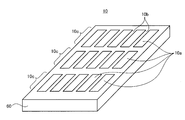
- FIG. 2 is a perspective view schematically showing the structure of the magnetic disk shown in FIG.
- FIG. 2 shows a part cut out from a disk-shaped magnetic disk.
- the magnetic disk 10 shown in FIG. 2 has a structure in which a plurality of magnetic dots 10 a are arranged in a regular arrangement on a glass substrate 60. Information corresponding to 1 bit is magnetically recorded on each of the magnetic dots 10a.
- the magnetic dots 10 a are arranged in a circle around the center of the magnetic disk 10.
- the row of magnetic dots arranged in this way forms a track 10c.
- the glass substrate 60 corresponds to an example of the substrate in the basic form described above.
- the magnetic dot 10a corresponds to an example of the magnetic part in the basic form described above, and also corresponds to an example of the magnetic dot in the application form described above corresponding to the bit patterned magnetic storage medium.
- an interdot separation zone 10b in which the magnetic anisotropy and the saturation magnetization are lower than the magnetic anisotropy and the saturation magnetization of the magnetic dot 10a is formed between the magnetic dots 10a.
- the interdot dot band 10b magnetically divides between the magnetic dots 10a. That is, the magnetic interaction between the magnetic dots 10a is reduced by the interdot dot band 10b.
- This inter-dot dividing band 10b corresponds to an example of the low magnetic portion in the above-described basic form, and also corresponds to an example of the inter-dot dividing band in the above-described applied form corresponding to the bit-patterned magnetic storage medium. .
- the magnetic interaction between the magnetic dots 10a is small, the magnetic interaction between the tracks 10c is small when recording / reproducing information on the magnetic dots 10a, so that there is little magnetic interference between the tracks. .
- the boundary of recorded information bits does not fluctuate due to heat, so that a so-called thermal fluctuation phenomenon is also avoided. Therefore, according to the bit patterned magnetic disk 10 as shown in FIG. 2, since the track width can be reduced and the recording bit length can be shortened, a magnetic recording medium having a high recording density can be realized.
- a method for manufacturing the magnetic disk 10 will be described below.
- the manufacturing method of the magnetic disk 10 corresponds to a specific embodiment of the magnetic storage medium manufacturing method described above with respect to the basic mode.
- the ion implantation process is a process in which ions are locally implanted between the plurality of locations using a plurality of locations regularly arranged in the direction in which the magnetic film spreads as the protection region.
- This application mode corresponds to a magnetic storage medium manufacturing method in which a bit patterned magnetic storage medium is manufactured. Since the bit patterned magnetic storage medium effectively avoids interference and thermal fluctuation phenomena as described above, the above-described application mode in which such a bit patterned magnetic storage medium is manufactured is preferable. It is. The method of manufacturing the magnetic disk 10 described below corresponds to a specific embodiment of this application mode.
- the magnetic disk manufacturing method of the present embodiment is a magnetic disk manufacturing method for mass-producing the magnetic disk 10 shown in FIGS. 1 and 2 by lot production.
- An ion doping method is used for manufacturing individual magnetic disks 10 in mass production.
- This comparative example is a type of manufacturing method in which a bit patterned magnetic storage medium is manufactured by etching and filling with a nonmagnetic material.
- FIG. 3 is a diagram showing a manufacturing method of a type in which a bit patterned magnetic storage medium is manufactured by etching and filling with a nonmagnetic material.
- the magnetic film 2 is formed on the substrate 1 in the film forming step (A).
- a resist 3 made of an ultraviolet curable resin is applied on the magnetic film 2, and a mold 4 having nano-sized holes 4 a is placed on the resist 3.
- the resist 3 enters the nano-sized hole 4a, and the dots 3a of the resist 3 are formed.
- the resist 3 is irradiated with ultraviolet rays through the mold 4, so that the resist 3 is cured and the dots 3 a are printed on the magnetic film 2. Further, after the resist 3 is cured, the mold 4 is removed.
- etching is performed in the etching step (C), so that the magnetic film is removed leaving the magnetic dots 2 a protected by the dots 3 a of the resist 3.
- the dots 3 a of the resist 3 are removed by chemical treatment, and only the magnetic dots 2 a remain on the substrate 1.
- the space between the magnetic dots 2a is filled with a nonmagnetic material. Thereafter, the surface is flattened through a flattening step (E), whereby the bit patterned magnetic storage medium 6 is completed (F).
- FIG. 4 is an explanatory diagram for explaining the ion doping method.
- FIG. 4 shows an underlayer 61, a magnetic film 62, a protective layer 63, and a resist pattern 64 that are formed on the glass substrate 60 prior to ion implantation.
- the glass substrate 60 that has been thoroughly cleaned is set in a magnetron sputtering apparatus and evacuated to 5 ⁇ 10 ⁇ 5 Pa or less. Thereafter, the glass substrate 60 is not heated, and the (111) crystal orientation of fcc-Pd having a film thickness of 3 nm is performed at an Ar gas pressure of 0.67 Pa. 60 is formed.
- the magnetic film 62 has an artificial lattice structure in which Co atomic layers and Pd atomic layers are alternately stacked.
- the magnetic film 62 having the artificial lattice structure is continuously formed with the Co monoatomic layer and the Pd at an Ar gas pressure of 0.67 Pa without returning the magnetron sputtering apparatus to atmospheric pressure. It is formed by repeatedly laminating a single atomic layer.
- a protective layer 63 made of diamond-like carbon and having a thickness of 4 nm is formed on the magnetic film 62. Then, a resist is applied on the protective layer 63, and a columnar resist having a rectangular cross section of 9 nm ⁇ 27 nm corresponding to the outer shape of the magnetic dot 10a of FIG. A pattern 64 is formed.
- either one of oxygen ions and nitrogen ions 65 is irradiated from above the resist pattern 64.
- the irradiated ions 65 are implanted into the magnetic film 62.
- the acceleration voltage in the ion implantation at this time is set so that the ions 65 are implanted into the central portion of the magnetic film 62.
- the acceleration voltage of the ions 65 is preferably 1 keV or more and 10 keV or less in consideration of a realistic magnetic film thickness and damage to the magnetic film during ion implantation.
- the ions 65 directed toward the resist pattern 64 remain in the resist pattern 64, and the ions 65 directed toward the gap between the resist patterns 64 are implanted into the magnetic film 62.
- saturation magnetization and magnetic anisotropy are reduced in the magnetic film 62 other than the region protected by the resist pattern 64.
- the region in which the saturation magnetization and magnetic anisotropy are reduced is the interdot separation band 10b in FIG.
- a region in which saturation magnetization and magnetic anisotropy are maintained by being protected by the resist pattern 64 becomes the magnetic dot 10a.
- the resist pattern 64 is removed by SCl cleaning, and the magnetic disk 10 of FIG. 2 is completed.
- the degree of disappearance of saturation magnetization due to ion implantation depends on the following conditions during manufacturing by sputtering.
- the conditions at the time of manufacturing by sputtering include conditions such as the thickness of a magnetic film obtained by sputtering, the purity of a target used in sputtering, and gas pressure.
- the degree of decrease in the magnetization reversal field also depends on these conditions.
- the ion doping method is applied to mass production in lot production while avoiding variations in the magnetization reversal magnetic field for each lot.
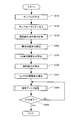
- FIG. 5 is a flowchart showing the magnetic disk manufacturing method of the first embodiment.
- the magnetic disks shown in FIGS. 1 and 2 are mass-produced by lot production using the ion doping method.
- the disappearance degree of saturation magnetization that would be caused by ion implantation at the time of mass production is grasped using a sample.
- the determination of the disappearance degree using this sample is performed by a series of processes from step S101 to step S103 described below.
- step S101 the next laminate is created as a sample.
- 4 is a laminate in which an underlayer, a magnetic film, and a protective layer equivalent to the underlayer 61, the magnetic film 62, and the protective layer 63 in FIG. 4 are laminated on a glass substrate equivalent to the glass substrate 60 in FIG. .
- Each layer in this sample is formed under the same numerical conditions as those described with reference to FIG.
- the layer thickness ratio of the Co atomic layer to the Pd atomic layer is determined in advance by the same process as that of Step S105 described later. Desired.
- a sample magnetic film is created with the obtained sample layer thickness ratio. The details of how to obtain the layer thickness ratio in the magnetic film of this sample will be described together with the description of the processing in step S105.
- the magnetic film of this sample has a Pd atomic layer thickness of 0.7 nm in the artificial lattice structure.
- the layer thickness of the Co atomic layer is a value obtained by multiplying the 0.7 nm layer thickness by the sample layer thickness ratio.
- a pair of an atomic layer of Pd and an atomic layer of Co is regarded as a kind of layer as a unit of lamination.
- the sample magnetic layer is formed of 20 layers.
- step S101 corresponds to an example of the first magnetic film forming process in the basic mode described above.
- step S102 first, the saturation magnetization of the magnetic film in the sample is measured. Thereafter, ion implantation is performed on the sample.
- ion implantation conditions equivalent to the ion implantation conditions described with reference to FIG. 4 are used as ion implantation conditions such as ion species and acceleration voltage.
- the processing in step S102 corresponds to an example of the first ion implantation process in the basic mode described above.
- step S103 the saturation magnetization of the magnetic film in the sample after ion implantation is measured. Then, by dividing the measured saturation magnetization after ion implantation by the saturation magnetization before ion implantation measured in step S102, the disappearance degree of saturation magnetization by ion implantation is obtained.
- the calculated saturation magnetization disappearance is considered to correspond to the saturation magnetization disappearance that will be caused by the subsequent ion implantation during mass production.
- the processing in step S103 corresponds to an example of the disappearance degree measurement process in the basic form described above.
- step S103 the saturation magnetization disappearance obtained in step S103 is 90%.
- step S104 The following processing is executed using the disappearance degree obtained in step S103 (step S104).
- the magnetization reversal magnetic field at the magnetic dot 10a is designed. It is executed on the assumption that it becomes equal to the magnetization reversal field above. Under this assumption, the anisotropic magnetic field of the original magnetic layer before saturation magnetization disappears by ion implantation is calculated.
- this anisotropic magnetic field is calculated using a so-called LLG (Landau-Liftshitz-Gilbert) equation, which is a mathematical model expressing the magnetic characteristics of a magnetic film or the like.
- an equation for obtaining the anisotropic magnetic field of the magnetic dot 10a which is obtained by modifying this LLG equation and using the saturation magnetization disappearance in the interdot separation zone 10b of FIG. 2 as a variable, is used. .
- step S104 the designed magnetization switching magnetic field is substituted for the magnetization switching magnetic field that is one of the parameters in this equation.
- the anisotropic magnetic field of the magnetic dots 10a is equal to the anisotropic magnetic field of the magnetic film before ion implantation in the ion doping method.
- the saturation magnetization disappearance in the interdot separation zone 10b is the saturation magnetization disappearance due to the ion implantation. That is, the expression used in the process of step S104 is an expression representing a dependency relationship in which the anisotropic magnetic field of the magnetic film before ion implantation depends on the saturation magnetization disappearance level due to ion implantation.
- the process of step S104 corresponds to an example of an anisotropic magnetic field calculation process in the basic form described above.
- the dependency represented by the equation derived from the LLG equation is referred to as saturation magnetization disappearance dependency of the anisotropic magnetic field.
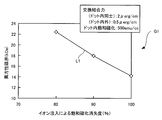
- FIG. 6 is a graph showing the saturation magnetization disappearance dependence of the anisotropic magnetic field represented by the formula used in step S104 of FIG.
- FIG. 6 shows a graph G1 showing the saturation magnetization disappearance dependence of the anisotropic magnetic field when a 5 kOe magnetization switching magnetic field is adopted as the designed magnetization switching magnetic field.
- the external dimension (vertical ⁇ horizontal) of the magnetic dot 10a is set to a designed value of 9 nm ⁇ 27 nm.
- the saturation magnetization of the magnetic dot 10a is set to 500 emu / cc, which is an empirical predicted value
- the anisotropic magnetic field of the interdot separation zone 10b is also set to 100 Oe, which is an empirical predicted value
- the exchange coupling force in the magnetic dot 10a is also set to 2 ⁇ erg / cm, which is an empirical predicted value
- the exchange coupling force between the magnetic dot 10a and the interdot separation band 10b is also an empirical predicted value of 0. .5 ⁇ erg / cm.
- the anisotropic magnetic field of the magnetic film 62 before the saturation magnetization disappears becomes 18 kOe.
- the anisotropic magnetic field (sample anisotropic magnetic field) for obtaining the layer thickness ratio (sample layer thickness ratio) of the Co atomic layer to the Pd atomic layer in the sample created in step S101 is: It is obtained by the same process as the process of step S104. However, in this embodiment, the sample anisotropic magnetic field is obtained under the assumption that the saturation magnetization disappearance due to ion implantation is 100%. According to the graph G1 in FIG. 6, this sample anisotropic magnetic field is 14 kOe.
- the anisotropic magnetic field obtained based on the disappearance degree obtained in step S103 in the process of step S104 is the anisotropy in the magnetic film actually formed during mass production as will be described later. Magnetic field. Therefore, hereinafter, the anisotropic magnetic field calculated in step S104 is referred to as an actual anisotropic magnetic field in distinction from the sample anisotropic magnetic field.
- step S104 When the actual anisotropic magnetic field is calculated in step S104, the following conditions necessary for realizing the actual anisotropic magnetic field in the magnetic film 62 are obtained (step S105).
- the magnetic film 62 subjected to ion implantation is a magnetic film having an artificial lattice structure in which Co atomic layers and Pd atomic layers are alternately stacked as described above.
- the anisotropic magnetic field in the magnetic film depends on the layer thickness ratio of the Co atomic layer to the Pd atomic layer. That is, the anisotropic magnetic field can be adjusted by adopting the artificial lattice structure as described above as the magnetic film 62 and adjusting the layer thickness ratio of the Co atomic layer. Accordingly, in step S105, a desired layer thickness ratio of the Co atomic layer is obtained as a condition necessary for realizing the actual anisotropic magnetic field obtained in step S104.
- the layer thickness ratio is obtained based on the following measurement data prepared in advance. That is, the measurement data represents a dependency relationship in which the anisotropic magnetic field depends on the layer thickness ratio of the Co atomic layer.
- the dependency represented by the measurement data is referred to as the layer thickness ratio dependency of the anisotropic magnetic field.
- This measurement data was obtained by forming a plurality of magnetic films having different Co atomic layer thickness ratios and measuring the anisotropic magnetic field in each magnetic film.
- step S105 the layer thickness ratio corresponding to the actual anisotropic magnetic field calculated in step S104 is obtained based on such measurement data.
- FIG. 7 is a graph showing an example of measurement data used in step S105 of FIG.
- FIG. 7 shows a graph G2 in which measurement data representing the dependence of the anisotropic magnetic field on the layer thickness ratio is plotted.
- the graph G2 includes a line L2 representing the layer thickness ratio dependence of the anisotropic magnetic field.
- the graph G2 also includes a line L3 representing a dependency relationship in which the saturation magnetization of the magnetic film 62 before ion implantation depends on the layer thickness ratio of the Co atomic layer.
- the dependency represented by the line L3 is referred to as layer thickness ratio dependency of saturation magnetization.
- the line L3 representing the layer thickness ratio dependency of the saturation magnetization is used in step S106 described later in FIG.
- two lines L2 and L3 shown in the graph G2 represent measurement data obtained for the magnetic film having an artificial lattice structure in which the thickness of the atomic layer of Pd is 0.7 nm and the number of stacks is 20 layers. Is.
- the number of layers (20 layers) on which the measurement data is based is referred to as the default number of layers.
- the actual anisotropic magnetic field obtained in step S104 corresponding to the saturation magnetization disappearance (90%) obtained in step S103 is 18 kOe as described above.
- the layer thickness ratio (hereinafter referred to as the actual layer thickness ratio) for obtaining this actual anisotropic magnetic field is approximately 0. .42.
- the sample layer thickness ratio in the sample created in step S101 is obtained by the same process as the process in step S105.
- the sample anisotropic magnetic field is 14 kOe as described above, the sample layer thickness ratio is 0.72 according to the graph G2 in FIG.
- step S101 a sample having a magnetic film having an artificial lattice structure in which a Pd atomic layer and a Co atomic layer are stacked at the sample layer thickness ratio obtained by the same processing as in step S105 is formed. It will be.
- the saturation magnetization (hereinafter referred to as the actual saturation magnetization) in the magnetic film having the artificial lattice structure in which the layer thickness ratio of the Co atomic layer is the actual layer thickness ratio is obtained.
- saturation magnetization (hereinafter referred to as sample saturation magnetization) in the magnetic film of the sample is also obtained.
- the line L3 representing the layer thickness ratio dependence of the saturation magnetization in the graph G2 in FIG. 7 is used.
- step S106 When two types of saturation magnetization are obtained in step S106, the actual number of layers in the magnetic film having the artificial lattice structure is obtained as follows based on the saturation magnetization (step S107).
- the actual number of layers is determined such that the product of the actual saturation magnetization and the actual number of layers is 90% or more of the product of the sample saturation magnetization and the default number of layers.
- This method of determining the actual number of layers is based on the following reasons.
- information reproduction on a magnetic disk is performed by detecting a leakage magnetic field generated by magnetization carrying information in a magnetic dot by a magnetic head.
- the reproduction signal obtained by the magnetic head increases as the saturation magnetization of the magnetic dots increases or as the volume of the magnetic dots increases. For this reason, for example, when it is assumed that the saturation magnetization is small and a reproduction signal of a desired level cannot be obtained, the reproduction signal of a desired level is realized by increasing the volume by slightly thickening the magnetic dots. It becomes possible.
- the magnetic dots have an artificial lattice structure as in the present embodiment, it is possible to realize a reproduction signal having a desired level as described above by increasing the number of layers in the artificial lattice structure.
- the reproduction signal of the desired level is The developer found this to be achieved.
- the level of the reproduction signal obtained with the magnetic dots when the interdot separation band is formed with a saturation magnetization disappearance of 100% is adopted as the target level.
- the magnetic film of the above sample is formed with a layer thickness ratio obtained on the assumption that the saturation magnetization disappearance is 100 percent. Therefore, in step S107 in FIG. 5, the actual number of stacked layers is such that the product of the actual saturation magnetization and the actual number of stacked layers is 90% or more of the product of the sample saturated magnetization and the default number of stacked layers. Is required.
- the sample saturation magnetization is 550 emu / cc
- the default number of layers is 20
- 90 percent of the product of both is 9900.
- the actual saturation magnetization is 450 emu / cc
- the actual number of stacked layers is 22 or more.
- step S107 By the processing up to step S107 described above, the layer thickness ratio and the number of stacks necessary for realizing the actual anisotropic magnetic field calculated in step S105 are obtained.
- step S108 a process using the layer thickness ratio and the number of layers is executed.
- FIG. 8 is a diagram showing details of the magnetic disk manufacturing process (step S108).
- an underlayer 61, a magnetic film 62, and a protective layer 63 shown in FIG. 8 are not shown for the sake of clarity.
- This film forming step (A) corresponds to an example of a second magnetic film forming process in the basic mode of the magnetic storage medium manufacturing method described above.
- the magnetic film 62 formed in this film forming step (A) has an artificial lattice structure in which Co atomic layers 62a and Pd atomic layers 62b are alternately stacked. is doing. And the artificial lattice structure here is constructed
- the actual anisotropic magnetic field calculated in step S102 of FIG. 5 can be realized by the artificial lattice structure having the layer thickness ratio obtained in step S105.
- both the first magnetic film forming process and the second magnetic film forming process form a magnetic film having an artificial lattice structure in which Co atomic layers and Pd atomic layers are alternately stacked. It has become a process.
- the layer thickness of the Co atomic layer with respect to the Pd atomic layer required for realizing the anisotropic magnetic field calculated in the anisotropic magnetic field calculation process with the magnetic film having the artificial lattice structure is described. It has a layer thickness ratio calculation process for calculating the ratio.
- the second magnetic film formation process includes the artificial atomic layer in which the Co atomic layer and the Pd atomic layer are alternately stacked at the layer thickness ratio calculated in the layer thickness ratio calculation process. This is a process of forming a magnetic film having a lattice structure.
- the desired anisotropy calculated in the anisotropic magnetic field calculation process can be achieved by a simple method of appropriately adjusting the layer thickness ratio of the Co atomic layer in the magnetic film having the artificial lattice structure.
- a magnetic field can be realized.
- step S105 in FIG. 5 corresponds to an example of a layer thickness ratio calculation process in this applied form.
- 8 corresponds to an example of a second magnetic film forming process in this application mode.
- the level of the reproduction signal obtained from the actual magnetic disk 10 can be adjusted to the target level by the artificial lattice structure having the number of layers obtained in step S107. it can.
- the following application forms are more suitable for the above application forms employing magnetic films having an artificial lattice structure.
- This application form has a stacking number calculation process.
- This stacking number calculating process is a process of calculating the number of atomic layers in the magnetic film formed in the second magnetic film forming process. The calculation is based on the product of the saturation magnetization and the number of atomic layers in the magnetic film formed in the first magnetic film formation process, and in the magnetic film formed in the second magnetic film formation process. This is executed so that the product of the saturation magnetization and the number of atomic layers satisfies a predetermined degree of approximation.
- the second magnetic film forming process is a process of forming the artificial lattice structure magnetic film by stacking the atomic layers having the number of atomic layers calculated in the stacking number calculating process. Yes.
- a magnetic film that generates a leakage magnetic field of almost the same level as the leakage magnetic field generated from the magnetic film formed in the first magnetic film formation process is formed in the second magnetic film formation process.
- the Rukoto The level of the leakage magnetic field generated from the magnetic film affects the level of a reproduction signal obtained from a bit patterned magnetic disk or the like formed using the magnetic film. Therefore, according to this application mode, a reproduction signal of a desired level can be obtained by a simple operation such as forming a magnetic film with saturation magnetization and the number of stacked layers so that a desired leakage magnetic field is generated in the first magnetic film forming process. The resulting magnetic disk can be obtained.
- step S107 in FIG. 5 corresponds to an example of a stacking number calculation process in this applied form.
- the product of the sample saturation magnetization and the default number of layers is the product of “the product of the saturation magnetization and the number of atomic layers in the magnetic film formed in the first magnetic film formation process” in this application. It corresponds to an example.
- the product of the actual saturation magnetization and the actual number of stacked layers is referred to as “product of the saturation magnetization and the number of atomic layers in the magnetic film formed in the second magnetic film forming process” referred to in this application mode. It corresponds to an example.
- an approximation degree of 90% or more is adopted as an example of the “approximation degree” in this application form.
- the film forming step (A) in FIG. 8 corresponds to an example of a second magnetic film forming process in this application mode.
- the nanoimprint step (B) is performed.
- a resist made of an ultraviolet curable resin is applied on the magnetic film 62, and a mold 66 having nano-sized holes 66a is placed on the resist.
- the resist enters the nano-sized hole 66a, and the resist pattern 64 shown in FIG. 4 is formed.
- the resist is cured by irradiating the resist with ultraviolet rays through the mold 66, and the resist pattern 64 is printed on the magnetic film 62. Further, the mold 66 is removed after the resist is cured.
- the process proceeds to the ion implantation process (C).
- this ion implantation step (C) ions are irradiated from above the magnetic film 62 on which the resist pattern 64 is printed. As a result, ions irradiated to a portion other than the resist pattern 64 are implanted into the magnetic film 62.
- This ion implantation step (C) corresponds to an example of the ion implantation step in the basic form described above.
- This ion implantation step (C) also corresponds to an example of the second ion implantation process in the above-described applied mode corresponding to the manufacture of the bit patterned magnetic storage medium.
- one of oxygen ions and nitrogen ions is used as the implanted ions. These ions can surely reduce the anisotropic magnetic field and saturation magnetization in the magnetic film 62 of the artificial lattice structure of the present embodiment and the magnetic film of the Co—Cr—Pt alloy in the second embodiment described later. it can.
- the application mode in which the second ion implantation process is a process using one of oxygen ions and nitrogen ions as the ions is preferable to the basic mode described above. I mean.
- This application form has a mask formation process.
- This mask formation process is a process of forming a mask that inhibits ion implantation into the protective region on the magnetic film.
- the second ion implantation process applies ions from above the magnetic film on which the mask is formed, so that other regions except for the protection region protected by the mask are applied. It is a process of implanting the ions locally.
- the nanoimprint process (B) in FIG. 8 corresponds to an example of a mask formation process in this application mode, and the ion implantation process (C) also corresponds to an example of a second ion implantation process in this application mode.
- an application mode in which the mask formation process is a process of forming the mask with a resist is more preferable. Also. In contrast to the above preferred application mode having a mask formation process, an application mode in which the mask formation process is a process of forming the mask with a resist by a nanoimprint process is further preferable.
- Resist mask formation is technically stable and accurate mask formation can be expected, and nanoimprint process mask formation is preferable because it can easily create a nano-level mask pattern.
- the nanoimprint process (B) shown in FIG. 8 also corresponds to an example of a mask formation process in these more preferable applications.
- the resist is not completely removed even at the location where ions are to be implanted.
- ions pass through the resist and are injected into the magnetic film 62.
- the resist is thick (that is, where the resist pattern 64 is formed), the ions stop at the resist and do not reach the magnetic film. . For this reason, a desired dot pattern can be formed.
- the acceleration voltage of ions is set so that ions are implanted into the center of the magnetic film 62.
- This acceleration voltage varies depending on the ion species, and varies depending on the depth to the magnetic film center and the material.
- the resist pattern 64 is removed by chemical treatment.
- an interdot separation band 10b that divides the magnetic interaction between the magnetic dots 10a is formed between the magnetic dots 10a.
- the disk 10 is completed (D).
- the saturation magnetization of the magnetic film 62 that has undergone ion implantation in the above-described ion implantation step (C) is the saturation magnetization loss degree grasped in step S101 of FIG. 5 (in this example, 90 percent). ) Disappears. As a result, some saturation magnetization remains in the interdot separation zone 10b formed by ion implantation. The saturation magnetization remaining in the interdot separation zone 10b reduces the magnetization reversal field in the magnetic dot 10a.
- the anisotropic magnetic field of the magnetic film 62 is calculated in step S104, and the designed magnetization reversal magnetic field in anticipation of such reduction. Is adjusted to an anisotropic magnetic field.
- the bit patterned magnetic disk 10 having the designed magnetization reversal magnetic field is manufactured regardless of the saturation magnetization disappearance.
- the saturation magnetization of the magnetic film 62 affects the level of the reproduction signal obtained for the magnetic dot 10a.
- the number of stacked layers in the magnetic film 62 having an artificial lattice structure is adjusted to the appropriate number of layers calculated in step S102. As a result, in this embodiment, the bit patterned magnetic disk 10 from which a desired level of reproduction signal is obtained is manufactured.
- step S108 the magnetic disk manufacturing process shown in detail in FIG. 8 is performed until the number of magnetic disks 10 reaches a prescribed mass production number (step S109). (Yes determination) is repeated.
- the saturation magnetization disappearance is grasped for each lot. Then, based on the grasped saturation magnetization disappearance level, the bit patterned magnetic disk 10 having a designed magnetization reversal magnetic field and capable of obtaining a reproduction signal of a desired level is manufactured. As a result, the magnetic disk 10 in which the variation of the magnetization reversal magnetic field for each lot is suppressed is manufactured. Also, the HDD 100 mass-produced using these magnetic disks 10 is one in which variations in the magnetization reversal magnetic field of the mounted magnetic disk 10 are suppressed.
- the magnetic dots are made of a Co—Cr—Pt alloy, and as a result, the magnetic disk manufacturing method becomes a manufacturing method corresponding to the formation of a magnetic film with this Co—Cr—Pt alloy.
- FIG. 9 is a flowchart showing the magnetic disk manufacturing method of the second embodiment.
- sample preparation step S201
- ion implantation into the sample step S202
- the magnetic film in the sample is a magnetic film made of a Co—Cr—Pt alloy.
- the Pt composition ratio (sample composition ratio) in the sample magnetic film is obtained by the same process as the process of step S203 described later.
- a sample magnetic film is created with the calculated sample composition ratio. The details of how to obtain the composition ratio in the magnetic film of this sample will be described together with the description of the processing in step S203.
- the thickness of the sample magnetic film is 20 nm.
- step S201 in the present embodiment also corresponds to an example of the first magnetic film formation process in the basic form described above, and the process of step S202 also corresponds to an example of the first ion implantation process in the basic form.
- step S103 For the sample having the magnetic film made of the Co—Cr—Pt alloy, the measurement of the saturation magnetization disappearance (step S103) and the calculation of the anisotropic magnetic field (step S104) are the same as in the first embodiment. Executed.
- step S203 in the process of step S203 subsequent to step S104, the Pt composition ratio (hereinafter referred to as the actual composition ratio) from which an actual anisotropic magnetic field is obtained is obtained.
- the actual composition ratio hereinafter referred to as the actual composition ratio
- this composition ratio is obtained based on the following measurement data prepared in advance. That is, the measurement data is obtained by forming a plurality of magnetic films having different Pt composition ratios and measuring the anisotropic magnetic field in each magnetic film.
- This measurement data represents a dependency relationship in which the anisotropic magnetic field depends on the Pt composition ratio (hereinafter referred to as the Pt composition ratio dependency of the anisotropic magnetic field).
- step S203 the composition ratio corresponding to the anisotropic magnetic field calculated in step S102 is obtained based on the dependency of the anisotropic magnetic field on the Pt composition ratio.
- the saturation magnetization disappearance obtained in step S101 is 90% and the actual anisotropic magnetic field obtained in step S102 is 18 kOe.
- FIG. 10 is a graph showing an example of the dependence of the anisotropic magnetic field on the Pt composition ratio.
- FIG. 10 shows a graph G3 on which measurement data representing the dependence of the anisotropic magnetic field on the Pt composition ratio is plotted.
- the graph G3 includes a line L3 representing the dependence of the anisotropic magnetic field on the Pt composition ratio.
- This graph G3 also shows a line L5 representing a dependency relationship in which the saturation magnetization of the magnetic film before ion implantation depends on the Pt composition ratio (hereinafter referred to as the Pt composition ratio dependency of saturation magnetization). .
- This line L5 is used in step S204 described later in FIG.
- the two lines L4 and L5 shown in the graph G3 represent measurement data obtained for a magnetic film made of a Co—Cr—Pt alloy and having a thickness of 20 nm.
- the film thickness on which this measurement data is based is called the default film thickness.
- the actual composition ratio for obtaining the actual anisotropic magnetic field (18 kOe) is approximately 29 at percent.
- the sample composition ratio in the sample created in step S201 is obtained by the same process as the process in step S203.
- the sample anisotropic magnetic field is 14 kOe, as in the description of the first embodiment described above. Then, from the graph G2 of FIG. 7, the sample composition ratio corresponding to this sample anisotropic magnetic field is approximately 23 at percent.
- step S201 a sample having a magnetic film made of a Co—Cr—Pt alloy containing Pt at the sample composition ratio obtained by the same process as the process of step S203 is formed.
- Step S204 saturation magnetization (hereinafter referred to as sample saturation magnetization) in the magnetic film of the sample is also obtained.
- step S204 the actual film thickness of the magnetic film made of the Co—Cr—Pt alloy is then calculated based on the calculated saturation magnetization as follows. (Step S205).
- step S205 the actual film thickness is determined so that the product of the actual saturation magnetization and the actual film thickness is 90% or more of the product of the sample saturation magnetization and the default film thickness.
- the actual film thickness is 20 nm or more.
- the method for obtaining this film thickness is based on the following reasons.
- the saturation magnetization of the magnetic material is small and a reproduction signal of a desired level cannot be obtained, by increasing the volume by slightly thickening the magnetic dots at the design stage, It becomes possible to realize a reproduction signal of a desired level.
- the magnetic dot is a single-layer film made of a Co—Cr—Pt alloy as in this embodiment, it is possible to realize a reproduction signal having a desired level as described above by increasing the film thickness. .
- the product of the saturation magnetization and the actual film thickness is 90% or more of the product of the saturation magnetization and the film thickness at the magnetic dot from which a reproduction signal of a desired level is obtained, the reproduction at the desired level is performed. The developer found that the signal was achieved.
- the level of the reproduction signal obtained with the magnetic dots when the interdot separation band is formed with a saturation magnetization disappearance of 100% is adopted as the target level.
- the magnetic film of the above sample is formed with a composition ratio obtained on the assumption that the saturation magnetization disappearance is 100 percent. Therefore, in step S205 in FIG. 9, the actual film thickness so that the product of the actual saturation magnetization and the actual film thickness is 90% or more of the product of the sample saturation magnetization and the default film thickness. Is required.
- step S205 the composition ratio of Pt necessary for realizing the actual anisotropic magnetic field calculated in step S105 and the film necessary for realizing a desired level of reproduction signal Thickness is obtained.
- an anisotropic magnetic field exceeding about 18 kOe cannot be realized with a magnetic film made of a Co—Cr—Pt alloy.
- Such an anisotropic magnetic field corresponds to a saturation magnetization disappearance lower than 90% from the graph G1 in FIG. That is, in the present embodiment, a desired magnetization reversal magnetic field can be realized only when the saturation magnetization disappearance obtained in step S103 of FIG. 9 is 90% or more.
- the magnetic disk manufacturing process (step S206) using the composition ratio and the film thickness is then executed.
- This magnetic disk manufacturing process (step S206) is equivalent to the series of processes shown in FIG. 8 except that the magnetic film obtained in the film forming process is made of a Co—Cr—Pt alloy. Therefore, description of the magnetic disk manufacturing process (step S206) is omitted here.
- the magnetic film made of Co—Cr—Pt alloy having the Pt composition ratio obtained in step S203 ensures the actual anisotropic magnetic field calculated in step S104. Can be realized.
- both the first magnetic film forming process and the second magnetic film forming process are processes for forming a magnetic film made of a Co—Cr—Pt-based alloy.
- the second magnetic film forming process forms a magnetic film with the Co—Cr—Pt based alloy containing Pt at the composition ratio calculated in the composition ratio calculating process as the magnetic film. It has become a process.
- the desired anisotropy calculated in the anisotropic magnetic field calculation process can be obtained by a simple method of appropriately adjusting the composition ratio of Pt in the magnetic film made of a Co—Cr—Pt base alloy.
- a magnetic field can be realized.
- step S206 the film forming process executed in the magnetic disk manufacturing process (step S206) in FIG. 9 corresponds to an example of a second magnetic film forming process in this applied embodiment.
- the level of the reproduction signal obtained from the actual magnetic disk can be adjusted to the target level by the film thickness obtained in step S205.
- the following application forms are more preferable to the above application forms employing the magnetic film made of Co—Cr—Pt base alloy.
- This application form has a film thickness calculation process.
- This film thickness calculation process is a process of calculating the film thickness of the magnetic film formed in the second magnetic film formation process. Then, the calculation is performed with respect to the product of the saturation magnetization and the film thickness in the magnetic film formed in the first magnetic film forming process, and the saturation in the magnetic film formed in the second magnetic film forming process. The product of magnetization and film thickness is executed so as to satisfy a predetermined degree of approximation.
- the second magnetic film forming process is a process of forming a magnetic film made of a Co—Cr—Pt based alloy with the film thickness calculated in the stacking number calculating process.
- a reproduction signal of a desired level can be obtained by a simple operation of forming a magnetic film with a saturation magnetization and a film thickness that generates a desired leakage magnetic field in the first magnetic film formation process.
- a magnetic disk can be obtained.
- step S205 in FIG. 9 corresponds to an example of a film thickness calculation process in this applied form.
- the product of the sample saturation magnetization and the default film thickness is an example of “the product of the saturation magnetization and the film thickness in the magnetic film formed in the first magnetic film formation process” in this application. It corresponds to.
- the product of the actual sample saturation magnetization and the actual film thickness is expressed as “the saturation magnetization and film thickness in the magnetic film formed in the second magnetic film forming process” described in this application. It corresponds to an example of “product”.
- an approximation degree of 90% or more is adopted as an example of the “approximation degree” in this application form.
- the magnetic disk manufacturing process (step S206) is executed using the Pt composition ratio obtained in step S203 and the film thickness obtained in step S205. Thereby, in this magnetic disk manufacturing process (step S206), a bit patterned magnetic disk having a designed magnetization reversal magnetic field and obtaining a desired level of reproduction signal is manufactured regardless of the saturation magnetization disappearance. It will be.
- this magnetic disk manufacturing process (step S206) is repeated until the number of magnetic disks reaches a prescribed mass production number (Yes determination in step S109).
- a magnetic disk in which the variation of the magnetization reversal magnetic field for each lot is suppressed is manufactured as in the magnetic disk manufacturing method of the first embodiment. Become. Also, HDDs mass-produced using these magnetic disks are those in which variations in the magnetization reversal magnetic field of the mounted magnetic disk are suppressed.
- bit patterned magnetic storage medium is illustrated as an example of the magnetic storage medium.
- the magnetic storage medium is not limited to the bit patterned type, and may be, for example, a discrete track type. good.
- the Co—Cr—Pt alloy is exemplified as an example of the Co—Cr—Pt base alloy forming the magnetic film, but the Co—Cr—Pt base alloy is not limited to this.
- the Co—Cr—Pt based alloy may be an alloy in which other elements are added to the Co—Cr—Pt alloy within a composition range that does not impair the magnetic properties of the Co—Cr—Pt alloy.
- a resist pattern as a preferred mask for forming magnetic dots is exemplified.
- a process may be used in which ion implantation is performed by placing a stencil mask close to the medium surface so as not to contact the medium surface. According to this process, the steps of resist coating and resist removal can be omitted.
- the nanoimprint process is shown to be used as the best example of resist patterning.
- electron beam exposure may be used for patterning.
Landscapes
- Manufacturing Of Magnetic Record Carriers (AREA)
- Magnetic Record Carriers (AREA)
Abstract
イオンドーピング方式を用いつつも、磁化反転磁界のバラつきを抑えて磁気記憶媒体を製造することができる製造方法、そのような製造方法で製造された磁気記憶媒体および情報記憶装置を提供することを目的とし、サンプルへのイオン注入による飽和磁化消失度を計測する消失度計測過程(ステップS103)と、計測された消失度で、保護領域を除いた他の領域について局所的に飽和磁化が消失したときに保護領域での磁化反転磁界が所定の磁化反転磁界と等しくなるという前提で、飽和磁化消失前の磁性膜の異方性磁界を算出する異方性磁界算出過程(ステップS104)と、その算出された異方性磁界を有する磁性膜を形成し、その磁性膜への局所的なイオン注入を行なってビットパターンド型の磁気ディスクを完成させる磁気ディスク製造処理(ステップS108)とを実行する。
Description
本件は、磁気記憶媒体を製造する製造方法、磁気記憶媒体、および磁気記憶媒体を備えた情報記憶装置に関する。
ハードディスクドライブ(HDD)は、データの高速アクセス及び高速転送が可能な大容量記憶装置として、情報記憶装置の主流になっている。このHDDについては、これまでも高い年率で面記録密度が高まっており、現在でもさらなる記録密度向上が求められている。
HDDの記録密度を向上させるためには、トラック幅の縮小や記録ビット長の短縮が必要であるが、トラック幅を縮小させると、隣接するトラック同士で、いわゆる磁気的な干渉が生じ易くなる。この干渉とは、即ち、記録時において磁気記録情報が目的外の隣接トラックに重ね書きされてしまう現象や、再生時において目的外の隣接トラックからの漏洩磁界によるクロストークが起きてしまう現象を総称したものである。これらの現象は、いずれも再生信号のS/N比の低下を招き、エラーレートの劣化を引き起こす要因となる。
一方、記録ビット長の短縮を進めると、磁気的な干渉の影響により記録ビットを長期間保存する性能が低下する熱揺らぎ現象が発生する。
これらの磁気的な干渉や熱揺らぎ現象を回避して短いビット長や高いトラック密度を実現する磁気記憶媒体として、ディスクリート・トラック型の磁気記憶媒体が提案されている。また、このディスクリート・トラック型の磁気記憶媒体の他に、ビットパターンド型の磁気記憶媒体も提案されている(例えば、特許文献1参照。)。特に、ビットパターンド型の磁気記憶媒体では、記録ビットの位置が予め決められており、その決められた記録ビットの位置に磁性材料のドット(磁性ドット)が形成され磁性ドットの相互間は非磁性材料で構成される。このように磁性ドットが互いに分離されていると磁性ドットどうしの磁気的相互作用が小さく、上述した干渉や熱揺らぎ現象が回避される。
ここで、従来、ビットパターンド型の磁気記憶媒体の多くは、次のような製造方法により製造されている。この製造方法では、まず、基板上に一様な磁性膜が形成される。その後、その磁性膜から、ビットとして利用する領域を除いた他の領域が、エッチング等の手法により除去されることで磁性ドットが形成される。そして、その除去された領域に非磁性材料が充填されることで、磁性ドットどうしを磁気的に分断するドット間分断帯が形成される。このような一連の処理によりビットパターンド型の磁気記憶媒体が得られることとなる。
ここで、このような従来の製造方法では、磁性ドットとドット分断帯とで厚みに差が生じやすい。そのため、このような従来の製造方法では、磁気記憶媒体上での磁気ヘッドの浮上特性を安定なものとするために、磁気記憶媒体の表面について精度の高い平坦化が必要となる。そのため、非常に複雑な製造プロセスを行う必要があるという課題や、製造コストが増大するという課題が生じる。
そこで、イオンを磁性膜に注入して局所的に磁気特性を変化させることで磁性ドットの分離状態を形成する加工方法(イオンドーピング方式)が提案されている(例えば、特許文献2参照。)。
このイオンドーピング方式によれば、イオンを注入して磁気特性を変えるため、エッチングや充填、平坦化等の複雑な製造プロセスが必要なくなり、製造コストの増加を大幅に抑えることが可能となる。
しかしながら、上述のイオンドーピング方式を採用した磁気記憶媒体の製造方法では、例えばロット生産を行った場合等に、磁性ドット内の磁化の反転に要する磁化反転磁界がロット毎にバラつく等といった不具合がしばしば生じている。
尚、ここまで、ビットパターンド型の磁気記憶媒体を例に挙げて、イオンドーピング方式で磁気記憶媒体を製造する際に磁化反転磁界がバラつくという課題について説明した。しかしながら、このような課題は、ビットパターンド型の磁気記憶媒体に限るものではなく、例えばディスクリート・トラック型の磁気記憶媒体にも当てはまる課題である。即ち、このような課題は、情報が磁気的に記録される磁性部と、磁性部の飽和磁化よりも小さい飽和磁化を有する低磁性部とを備えた磁気記憶媒体に共通して当てはまる課題である。
本件では上記事情に鑑み、イオンドーピング方式を用いつつも、磁化反転磁界のバラつきが抑えられた磁気記憶媒体を製造することができる製造方法、そのような製造方法で製造された磁気記憶媒体および情報記憶装置を提供することを目的とする。
まず、上記目的を達成する基本形態の磁気記憶媒体製造方法は、第1の磁性膜形成過程と、第1のイオン注入過程と、消失度計測過程と、異方性磁界算出過程と、第2の磁性膜形成過程と、第2のイオン注入過程とを有している。
第1の磁性膜形成過程は磁性膜を形成する過程である。
第1のイオン注入過程は上記磁性膜にイオン注入を行なう過程である。
消失度計測過程は、上記磁性膜における、上記第1のイオン注入過程でのイオン注入による飽和磁化の消失度を計測する過程である。
異方性磁界算出過程は、次の前提で実行される過程である。即ち、上記消失度計測過程で計測された消失度で上記磁性膜の飽和磁化が、所定の場所に設定された保護領域を除いた他の領域について局所的に消失したときにその保護領域での磁化反転磁界が所定の磁化反転磁界と等しくなるという前提である。そして、この異方性磁界算出過程は、この前提で、飽和磁化消失前の上記磁性膜の異方性磁界を算出する過程である。
第2の磁性膜形成過程は、基板上に、上記異方性磁界算出過程で算出された異方性磁界と同等な異方性磁界を有する磁性膜を、第1の磁性膜形成過程での磁性膜の形成条件と同等な形成条件で形成する過程である。
第2のイオン注入過程は、上記第2の磁性膜形成過程で形成された磁性膜に対して上記他の領域に相当する領域について局所的に、上記第1のイオン注入過程でのイオン注入条件と同等なイオン注入条件でイオン注入を行なう過程である。
次に、上記目的を達成する基本形態の磁気記憶媒体は、基板と、磁性部と、低磁性部とを備えている。
磁性部は、上記第1の磁性膜形成過程と、上記第1のイオン注入過程と、上記消失度計測過程と、上記異方性磁界算出過程と、上記第2の磁性膜形成過程とを経て形成された磁性膜を有し、情報が磁気的に記録されるものである。
低磁性部は、上記磁性部の磁性膜と連続した磁性膜への、局所的なイオン注入過程を経て形成された被注入膜を有し、その磁性部の飽和磁化よりも小さい飽和磁化を有するものである。また、この低磁性部を得るための局所的なイオン注入過程は、上記第1のイオン注入過程でのイオン注入条件と同等なイオン注入条件でイオン注入を行なう過程である。
また、上記目的を達成する基本形態の情報記憶装置は、上記磁気記憶媒体と、磁気ヘッドと、ヘッド位置制御機構とを備えたものである。
磁気ヘッドは、上記磁気記憶媒体に近接あるいは接触して磁性部に磁気的に情報の記録及び/又は再生を行うものである。
また、ヘッド位置制御機構は、上記磁気ヘッドを上記磁気記憶媒体表面に対して相対的に移動させて、その磁気ヘッドによる情報の記録及び/又は再生となる磁性部上にその磁気ヘッドを位置決めするものである。
本件によれば、イオンドーピング方式を用いつつも、磁化反転磁界のバラつきを抑えて磁気記憶媒体を製造することができる製造方法、そのような製造方法で製造された磁気記憶媒体および情報記憶装置を得ることができる。
以下、基本形態について上記説明した磁気記憶媒体製造方法、磁気記憶媒体、および情報記憶装置に対する具体的な実施形態として、第1および第2の2種類の実施形態を図面を参照して説明する。
まず、第1実施形態について説明する。
図1は、情報記憶装置の具体的な実施形態であるハードディスク装置(HDD)の内部構造を示す図である。
この図に示すハードディスク装置(HDD)100は、パーソナルコンピュータ等といった上位装置に組み込まれ、その上位装置における情報記憶手段として利用されるものである。
このハードディスク装置100には、円盤状の磁気ディスク10が、図の奥行き方向に重なって複数枚ハウジングH内に納められている。この磁気ディスク10は、上記で基本形態について説明した磁気記憶媒体の具体的な実施形態に相当する。
ここで、上述の磁気記憶媒体および情報記憶装置の基本形態に対し、次のような応用形態は好適である。この応用形態では、上記磁性部が、上記基板上に規則的に複数配列された、各々に情報が磁気的に記録される磁性ドットとなっている。また、この応用形態では、上記低磁性部が、上記磁性ドットの相互間に設けられた、その磁性ドット相互の磁気的結合を阻害するドット間分断帯となっている。
この応用形態は、ビット情報が記録される磁性ドットが予め基板上の各箇所に設けられているビットパターンド型の磁気記憶媒体に対応する。ビットパターンド型の磁気記憶媒体は、上述したように干渉や熱揺らぎ現象が効果的に回避されることから、そのようなビットパターンド型の磁気記憶媒体に対応する上記の応用形態は好適である。
図1の磁気ディスク10は、ビットパターンド型の磁気記憶媒体であり、この応用形態の具体的な一実施形態にも相当している。また、この磁気ディスク10は、各磁性ドットにおいて、表裏面に対して垂直な方向の磁化による磁気パターンで情報が記録されるいわゆる垂直磁気記憶媒体でもある。
この磁気ディスク10は、ハウジングH内においてディスク軸11を中心に回転する。
また、ハードディスク装置100のハウジングH内には、スイングアーム20、アクチュエータ30、および制御回路50も納められている。
スイングアーム20は、磁気ディスク10の表面に沿って移動するものである。そして、このスイングアーム20は、磁気ディスク10に対して情報の書き込みと読み出しとを行う磁気ヘッド21を先端に保持している。また、スイングアーム20は、ベアリング24によってハウジングHに回動自在に支持されている。そして、このスイングアーム20は、ベアリング24を中心として所定角度の範囲内で回動することによって、磁気ヘッド21を磁気ディスク10の表面に沿って移動させる。この磁気ヘッドが、上述の基本形態における磁気ヘッドの一例に相当する。
アクチュエータ30は、上記のスイングアーム20を駆動するものである。
制御回路50は、アクチュエータ30によるスイングアーム20の駆動、磁気ヘッド21による情報の読み書き、このHDD100と上位装置との情報の遣り取り等を制御するものである。
上記のスイングアーム20とベアリング24とアクチュエータ30と制御回路50とを合わせたものが、上述の基本形態におけるヘッド位置制御機構の一例に相当する。
図2は、図1に示す磁気ディスクの構造を模式的に示す斜視図である。
この図2には、円盤状の磁気ディスクから切り出された一部が示されている。
図2に示す磁気ディスク10は、ガラス基板60上に複数の磁性ドット10aが規則的な配列で並べられた構造を有している。磁性ドット10aのそれぞれには1ビット相当の情報が磁気的に記録される。磁性ドット10aは磁気ディスク10の中心の周りに周回状に並んでいる。そして、そのように並んだ磁性ドットの列はトラック10cを形成する。ガラス基板60は、上述の基本形態における基板の一例に相当する。また、磁性ドット10aは、上述の基本形態における磁性部の一例に相当し、ビットパターンド型の磁気記憶媒体に対応した上述の応用形態における磁性ドットの一例にも相当している。
また、磁性ドット10aの相互間は、磁気異方性および飽和磁化が磁性ドット10aの磁気異方性および飽和磁化よりも低いドット間分断帯10bとなっている。このドット間分断帯10bは、磁性ドット10aの相互間を磁気的に分断している。つまり、このドット間分断帯10bによって磁性ドット10aどうしの磁気的相互作用が小さくなっている。このドット間分断帯10bは、上述の基本形態における低磁性部の一例に相当し、ビットパターンド型の磁気記憶媒体に対応した上述の応用形態におけるドット間分断帯の一例にも相当している。
このように磁性ドット10aどうしの磁気的相互作用が小さいと、磁性ドット10aに対する情報の記録再生に際してトラック10c相互間での磁気的相互作用が小さいため、トラック相互間での磁気的な干渉が少ない。また、各磁性ドット10aでは、記録される情報ビットの境界が熱で揺らぐことがないので、いわゆる熱揺らぎ現象も回避される。従って、この図2に示すようなビットパターンド型の磁気ディスク10によれば、トラック幅の縮小や記録ビット長の短縮が可能であるので、高記録密度の磁気記憶媒体が実現可能である。
この磁気ディスク10の製造方法について以下に説明する。
この磁気ディスク10の製造方法が、基本形態について上記説明した磁気記憶媒体製造方法の具体的な実施形態に相当する。
ここで、この磁気記憶媒体製造方法の基本形態に対して、次のような応用形態は好適である。即ち、上記イオン注入過程が、上記保護領域として上記磁性膜が広がる方向に規則的に配列した複数箇所を用いて、その複数箇所の相互間に対して局所的にイオンを注入する過程であるという応用形態である。
この応用形態は、ビットパターンド型の磁気記憶媒体が製造される磁気記憶媒体製造方法に対応する。ビットパターンド型の磁気記憶媒体は、上述したように干渉や熱揺らぎ現象が効果的に回避されることから、そのようなビットパターンド型の磁気記憶媒体が製造される上記の応用形態は好適である。以下に説明する磁気ディスク10の製造方法は、この応用形態の具体的な一実施形態にも相当している。
ここで、本実施形態の磁気ディスク製造方法は、図1や図2に示す磁気ディスク10をロット生産により量産するための磁気ディスク製造方法である。そして、その量産における個々の磁気ディスク10の製造に、イオンドーピング方式が使われている。
以下、この本実施形態の磁気ディスク製造方法の説明に先立って、まず、この製造方法で使われるイオンドーピング方式と対比するための比較例について説明する。この比較例は、ビットパターンド型の磁気記憶媒体を、エッチングと非磁性材料の充填とによって製造するタイプの製造方法である。
図3は、ビットパターンド型の磁気記憶媒体を、エッチングと非磁性材料の充填とによって製造するタイプの製造方法を示す図である。
このタイプの製造方法では、まず、製膜工程(A)で、基板1上に磁性膜2が形成される。
次に、ナノインプリント工程(B)では、磁性膜2上に、紫外線硬化樹脂からなるレジスト3が塗布され、そのレジスト3に、ナノサイズの穴4aが空いたモールド4が載せられる。これによってレジスト3がそのナノサイズの穴4aに入ってレジスト3のドット3aが形成される。そして、そのモールド4越しにレジスト3に紫外線が照射されることでレジスト3が硬化してドット3aが磁性膜2上にプリントされる。また、レジスト3が硬化した後、モールド4は除去される。
その後、エッチング工程(C)でエッチングが行われることで、レジスト3のドット3aで保護された磁性ドット2aを残して磁性膜が除去される。エッチング後はレジスト3のドット3aは化学的処理で除去され、基板1上に磁性ドット2aのみが残る。
そして、充填工程(D)では、磁性ドット2aの相互間が非磁性材料で埋められる。その後、平坦化工程(E)を経て表面が平坦化されることでビットパターンド型の磁気記憶媒体6の完成(F)となる。
このようなタイプの製造方法によると、磁気記憶媒体6上での磁気ヘッドの浮上特性を安定なものとするために平坦化工程(E)では精度の高い平坦化が必要となる。そのため、非常に複雑な製造プロセスを行う必要があるという課題や、製造コストが増大するという課題が生じる。
一方、本実施形態では、上述したようにイオンドーピング方式が採用されている。
以下、この本実施形態の磁気ディスク製造方法で使われるイオンドーピング方式について説明する。
図4は、イオンドーピング方式について説明する説明図である。
この図4には、イオン注入に先立ってガラス基板60上に製膜される、下地層61、磁性膜62、保護層63、およびレジストパターン64が示されている。
以下、これらの各層の製膜について説明する。
尚、この図4についての以下の説明におけるマグネトロンスパッタ装置での条件や膜厚等といった様々な数値は、下記の値に限定されるものではなく、適宜に他の値を用いても良い。
本実施形態では、まず、よく洗浄されたガラス基板60がマグネトロンスパッタ装置にセットされ、5×10⁻⁵Pa以下まで真空排気される。その後、ガラス基板60を加熱せず0.67PaのArガス圧にて、(111)結晶配向した、膜厚が3nmのfcc-Pdが、磁性層を結晶配向させるための下地層61としてガラス基板60上に製膜される。
続いて、下地層61上に磁性膜62が形成される。本実施形態では、この磁性膜62は、Coの原子層とPdの原子層とが交互に積層されてなる人工格子構造を有している。この人工格子構造の磁性膜62は、下地層61の形成後、上記のマグネトロンスパッタ装置を大気圧に戻すことなく連続して、0.67PaのArガス圧にて、Coの単原子層とPdの単原子層とを繰り返し積層することで形成される。
磁性膜62を製膜した後には、ダイヤモンドライクカーボン製で膜厚が4nmの保護層63が磁性膜62上に製膜される。そして、この保護層63上にレジストが塗布され、ナノインプリントプロセスを用いて、図2の磁性ドット10aの外形に相当する9nm×27nmの矩形状の断面を有し、高さが50nmの柱状のレジストパターン64が形成される。
このように各層の製膜が終了すると、次にイオン注入が行なわれる。
イオン注入では、酸素イオン及び窒素イオンのうちいずれか一方のイオン65がレジストパターン64の上方から照射される。その結果、その照射されたイオン65が磁性膜62に注入される。また、このときのイオン注入における加速電圧は、磁性膜62の中心部へイオン65が注入されるように設定される。尚、イオン65の加速電圧は、現実的な磁性膜の膜厚や、イオン注入時における磁性膜へのダメージを考慮すると、1keV以上で、10keV以下であることが望ましい。
上記のようなイオン注入では、レジストパターン64に向かったイオン65は、このレジストパターン64内に留まり、レジストパターン64の間隙に向かったイオン65が磁性膜62に注入される。その結果、磁性膜62のうち、レジストパターン64で保護された領域以外の他の領域について飽和磁化や磁気異方性が低減される。これら飽和磁化や磁気異方性が低減された領域が、図2のドット間分断帯10bとなる。一方、レジストパターン64で保護されることで飽和磁化や磁気異方性が維持された領域が磁性ドット10aとなる。
このイオン注入の後、レジストパターン64がSCl洗浄によって除去され、図2の磁気ディスク10が完成する。
ここで、以上に説明したイオンドーピング方式では、多くの場合、上記のドット間分断帯10bに飽和磁化が若干残り、その残りに起因して磁性ドット10aにおける磁化反転磁界が低下する。さらに、イオン注入による飽和磁化の消失度は、スパッタ法による製造時の次のような諸条件に依存する。スパッタ法による製造時の諸条件とは、例えば、スパッタ法で得られる磁性膜の膜厚や、スパッタ法で使われるターゲットの純度やガス圧等といった条件である。この結果、磁化反転磁界の低下度合いもこれら諸条件に依存することとなる。
さらに、一般的に、ロット生産では、上記のような製造時の諸条件が、ロット毎に変わってしまう可能性が高い。そして、そのような諸条件の変動に起因した飽和磁化の消失度の変動によって磁化反転磁界の低下度合いが変わってしまう。その結果として、従来、イオンドーピング方式による磁気ディスクの製造方法では、この磁化反転磁界がロット毎にバラつく等といった不具合がしばしば生じることとなっている。
本実施形態の磁気ディスク製造方法では、以下に説明するように、磁化反転磁界のロット毎のバラつきが回避された上で、イオンドーピング方式が、ロット生産での量産に適用されている。
図5は、第1実施形態の磁気ディスク製造方法を示すフローチャートである。
このフローチャートが示す磁気ディスク製造方法では、図1および図2に示す磁気ディスクが、イオンドーピング方式を用いてロット生産で量産される。
この図5のフローチャートが示す製造方法では、まず、量産を開始する前に、その量産時のイオン注入によって生じるであろう飽和磁化の消失度が、サンプルを使って把握される。このサンプルを使った消失度の把握は、以下に説明するステップS101~ステップS103までの一連の処理によって行われる。
ステップS101の処理では、次の積層物がサンプルとして作成される。即ち、図4のガラス基板60と同等なガラス基板上に、図4の下地層61と磁性膜62と保護層63それぞれと同等な下地層と磁性膜と保護層が積層された積層物である。また、このサンプルにおける各層は、図4を参照して説明した数値条件と同じ数値条件で形成される。
尚、本実施形態では、このサンプルの磁性膜の人工格子構造における、Pdの原子層に対するCoの原子層の層厚比(サンプル層厚比)が、後述のステップS105の処理と同じ処理によって予め求められる。そして、ステップS101の処理では、サンプルの磁性膜が、その求められたサンプル層厚比で作成される。このサンプルの磁性膜における層厚比の求め方の詳細については、ステップS105の処理について説明するときに併せて説明する。
また、本実施形態では、このサンプルの磁性膜は、人工格子構造におけるPdの原子層の層厚は0.7nmとなっている。そして、Coの原子層の層厚は、この0.7nmの層厚に上記のサンプル層厚比を乗じた値となる。さらに、ここでは、Pdの原子層とCoの原子層との対が、積層の単位としての一種の層とみなされている。そして、サンプルの磁性層は、積層数が20層で形成されている。
このステップS101の処理が、上述の基本形態における第1の磁性膜形成過程の一例に相当する。
次に、ステップS102の処理では、まず、上記のサンプルにおける磁性膜の飽和磁化が測定される。その後、そのサンプルに対してイオン注入が行なわれる。このステップS102でのイオン注入では、イオン種や加速電圧等といったイオン注入条件として、図4を参照して説明したイオン注入条件と同等なイオン注入条件が使われる。このステップS102の処理が、上述の基本形態における第1のイオン注入過程の一例に相当する。
続くステップS103の処理において、イオン注入後のサンプルにおける磁性膜の飽和磁化が測定される。そして、その測定されたイオン注入後の飽和磁化を、ステップS102で測定されたイオン注入前の飽和磁化で除することで、イオン注入による飽和磁化の消失度が求められる。この求められた飽和磁化の消失度が、この後の量産時のイオン注入によって生じるであろう飽和磁化の消失度に相当するものとみなされる。このステップS103の処理が、上述の基本形態における消失度計測過程の一例に相当する。
以下、このステップS103で得られた飽和磁化消失度が、90パーセントであったと仮定して説明を続ける。
このステップS103で得られた消失度を使って、以下の処理が実行される(ステップS104)。この処理は、図2や図4のドット間分断帯10bが、ステップS103で得られた消失度で飽和磁化が消失して形成されたものであるときに磁性ドット10aでの磁化反転磁界が設計上の磁化反転磁界と等しくなるという前提で実行される。そして、この前提の下で、イオン注入による飽和磁化消失前の元々の磁性層の異方性磁界が算出される。
本実施形態では、この異方性磁界の算出には、磁性膜等における磁気特性を表現した数学モデルである、いわゆるLLG(Landau-Liftshitz-Gilbert)方程式が使われる。
本実施形態では、このLLG方程式を変形して得られる、図2のドット間分断帯10bでの飽和磁化消失度を変数とした、磁性ドット10aの異方性磁界を求めるための式が用いられる。
そして、ステップS104の処理では、この式におけるパラメータの1つである磁化反転磁界に設計上の磁化反転磁界が代入される。
ここで、磁性ドット10aの異方性磁界は、イオンドーピング方式におけるイオン注入前の磁性膜が有している異方性磁界に等しい。また、ドット間分断帯10bでの飽和磁化消失度とは、そのイオン注入による飽和磁化消失度のことである。つまり、このステップS104の処理で使われる式は、イオン注入前の磁性膜の異方性磁界がイオン注入による飽和磁化消失度に依存する依存関係を表わした式となっている。このステップS104の処理が、上述の基本形態における異方性磁界算出過程の一例に相当する。以下、このLLG方程式から導かれた式が表わす依存関係を、異方性磁界の飽和磁化消失度依存性と呼ぶ。
図6は、図5のステップS104で使われる式が表わす異方性磁界の飽和磁化消失度依存性を示すグラフである。
この図6には、設計上の磁化反転磁界として、5kOeの磁化反転磁界が採用されたときの、異方性磁界の飽和磁化消失度依存性を示すグラフG1が示されている。
そして、このグラフG1には、異方性磁界の飽和磁化消失度依存性を表わすラインL1が記載されている。
尚、このグラフG1では、磁化反転磁界の他にも、下記のようなパラメータが設定されている。まず、磁性ドット10aの外形寸法(縦×横)が、9nm×27nmという設計上の値に設定されている。
また、磁性ドット10aの飽和磁化が経験上の予測値である500emu/ccに設定され、ドット間分断帯10bの異方性磁界も経験上の予測値である100Oeに設定されている。さらに、磁性ドット10a内での交換結合力も経験上の予測値である2μerg/cmに設定され、磁性ドット10aとドット間分断帯10bとの間での交換結合力も経験上の予測値である0.5μerg/cmに設定されている。
このグラフG1から分かるように、上記の前提を満足する飽和磁化消失前の磁性膜62の異方性磁界は、飽和磁化消失度の増加に伴ってほぼ線形に低下する。
ここで、図5のステップS103で得られた飽和磁化消失度が90パーセントであるという上記の仮定によると、飽和磁化消失前の磁性膜62の異方性磁界は18kOeとなる。
さらに、本実施形態では、ステップS101で作成するサンプルにおけるPdの原子層に対するCoの原子層の層厚比(サンプル層厚比)を求めるための異方性磁界(サンプル異方性磁界)が、このステップS104の処理と同じ処理によって求められる。ただし、本実施形態では、このサンプル異方性磁界は、イオン注入による飽和磁化消失度が100パーセントであるという仮定の下で求められる。図6のグラフG1によると、このサンプル異方性磁界は14kOeとなる。
このサンプル異方性磁界に対し、ステップS104の処理においてステップS103で得られた消失度に基づいて求められる異方性磁界は、後述するように量産時に実際に形成される磁性膜における異方性磁界である。そこで、以下では、このステップS104で算出された異方性磁界を、上記のサンプル異方性磁界と区別して実際の異方性磁界と呼ぶ。
ステップS104において、実際の異方性磁界が算出されると、磁性膜62においてその実際の異方性磁界を実現するのに必要な、以下の条件が求められる(ステップS105)。
ここで、本実施形態では、イオン注入を受ける磁性膜62は、上述のようにCoの原子層とPdの原子層とが交互に積層された人工格子構造の磁性膜である。このような人工格子構造の磁性膜では、磁性膜における異方性磁界は、Pdの原子層に対するCoの原子層の層厚比に依存する。即ち、磁性膜62として、上記のような人工格子構造を採用しCoの原子層の層厚比を調整することで、異方性磁界を調整することができる。そこで、ステップS105では、上記のステップS104で得られた実際の異方性磁界を実現するのに必要な条件として、上記のCoの原子層の所望の層厚比が求められる。
ここで、本実施形態では、上記の層厚比は、予め用意された次のような測定データに基づいて求められる。即ち、異方性磁界がCoの原子層の層厚比に依存する依存関係を表わす測定データである。以下、この測定データが表わす依存関係を、異方性磁界の層厚比依存性と呼ぶ。この測定データは、Coの原子層の層厚比が互いに異なる複数の磁性膜を形成して各磁性膜における異方性磁界を測定することで得られたものである。ステップS105では、ステップS104で算出された実際の異方性磁界に対応する層厚比が、このような測定データに基づいて求められる。
図7は、図5のステップS105で用いられる測定データの一例を示すグラフである。
この図7には、異方性磁界の層厚比依存性を表わす測定データがプロットされたグラフG2が示されている。そして、このグラフG2には、異方性磁界の層厚比依存性を表わすラインL2が記載されている。
尚、このグラフG2には、イオン注入前の磁性膜62の飽和磁化がCoの原子層の層厚比に依存する依存関係を表わすラインL3も記載されている。このラインL3が表わす依存関係を、以下では、飽和磁化の層厚比依存性と呼ぶ。この飽和磁化の層厚比依存性を表わすラインL3については、図5における後述のステップS106で使われる。
また、このグラフG2に示す2つのラインL2,L3は、Pdの原子層の膜厚が0.7nmで、上記の積層数が20層の人工格子構造の磁性膜について得られた測定データを表わすものである。
以下、この測定データの前提となった積層数(20層)をデフォルトの積層数と呼ぶ。
ここでの例では、ステップS103で得られた飽和磁化消失度(90パーセント)に対応して上記のステップS104で得られる実際の異方性磁界は上述のように18kOeである。図7のグラフG2で異方性磁界の層厚比依存性を表わすラインL2から、この実際の異方性磁界を得るための層厚比(以下、実際の層厚比と呼ぶ)がおよそ0.42となる。
さらに、本実施形態では、ステップS101で作成するサンプルにおける上記のサンプル層厚比が、このステップS105の処理と同じ処理によって求められる。ここでの例では、上述したようにサンプル異方性磁界が14kOeであるので、図7のグラフG2によると、サンプル層厚比は0.72となる。
上記のステップS101では、このステップS105の処理と同じ処理によって求められたサンプル層厚比でPdの原子層とCoの原子層とが積層された人工格子構造の磁性膜を有するサンプルが形成されることとなる。
次に、図5のフローチャートでは、Coの原子層の層厚比が上記の実際の層厚比となっている人工格子構造の磁性膜における飽和磁化(以下、実際の飽和磁化と呼ぶ)が求められる(ステップS106)。さらに、このステップS106の処理では、上記のサンプルの磁性膜における飽和磁化(以下、サンプル飽和磁化と呼ぶ)も求められる。
このステップS106での2つの飽和磁化の算出には、上記の図7のグラフG2における飽和磁化の層厚比依存性を表わすラインL3が使われる。
このラインL3から、ステップS105で得られた実際の層厚比(0.42)に対応する実際の飽和磁化として、約450emu/ccという値が得られる。一方、サンプル層厚比(0.72)に対応するサンプル飽和磁化として、約550emu/ccという値が得られる。
ステップS106において2種類の飽和磁化が求められると、次に、それらの飽和磁化に基づいて、人工格子構造の磁性膜における実際の積層数が次のように求められる(ステップS107)。
本実施形態では、実際の飽和磁化と実際の積層数との積が、サンプル飽和磁化とデフォルトの積層数との積の90パーセント以上となるように、実際の積層数が決定される。
この実際の積層数の求め方は、次のような理由に基づいている。
一般に、磁気ディスクに対する情報再生は、磁性ドットにおいて情報を担持している磁化が発する漏れ磁界が磁気ヘッドによって検出されることで行われる。このとき、磁気ヘッドで得られる再生信号は、磁性ドットの飽和磁化が大きい程、あるいは磁性ドットの体積が大きい程大きくなる。このため、例えば飽和磁化が小さくて所望のレベルの再生信号が得られないことが想定される場合には、磁性ドットを若干厚めにして体積を増すことによって、所望のレベルの再生信号を実現することが可能となる。本実施形態のように磁性ドットが人工格子構造を有する場合には、人工格子構造における積層数を増やすことで、上記のような所望のレベルの再生信号を実現することができる。このとき、飽和磁化と積層数との積が、所望のレベルの再生信号が得られる磁性ドットでの飽和磁化と積層数との積の90パーセント以上であれば、その所望のレベルの再生信号が達成されることことを本件の開発者は見出した。
本実施形態では、ドット間分断帯が100パーセントの飽和磁化消失度で形成されたときの磁性ドットで得られる再生信号のレベルが、目標のレベルとして採用される。ここで、上記のサンプルの磁性膜は、100パーセントの飽和磁化消失度を前提として求められた層厚比で形成されたものである。そこで、図5のステップS107では、実際の飽和磁化と実際の積層数との積が、上記のサンプル飽和磁化とデフォルトの積層数との積の90パーセント以上となるように、その実際の積層数が求められる。
上述の具体例では、サンプル飽和磁化が550emu/ccであり、デフォルトの積層数が20層であって、両者の積の90パーセントが9900となる。一方で、実際の飽和磁化が450emu/ccであるので、実際の積層数は22層以上となる。
以上に説明したステップS107までの処理で、ステップS105で算出された実際の異方性磁界を実現するのに必要な層厚比と積層数とが得られる。
そして、このステップS107に続く磁気ディスク製造処理(ステップS108)において、それらの層厚比と積層数とを用いた処理が実行される。
図8は、磁気ディスク製造処理(ステップS108)の詳細を示す図である。
まず、製膜工程(A)で、ガラス基板60上に、図4に示す下地層61と磁性膜62と保護層63とが形成される。尚、この図8では、図4に示す下地層61と保護層63については図を見やすくするために図示が省略されている。
ここでの形成は、ステップS101においてサンプルを形成したときの、図4を参照して説明した各種数値条件と同等な数値条件で行なわれる。ただし、磁性膜62におけるCoの原子層62aの層厚比と、Coの原子層62aとPdの原子層62bとの組の積層数については、図5のステップS107までの処理で求められた層厚比と積層数とが用いられる。この製膜工程(A)は、上述した磁気記憶媒体製造方法の基本形態における第2の磁性膜形成過程の一例に相当する。
本実施形態では、上述したように、この製膜工程(A)で形成される磁性膜62は、Coの原子層62aとPdの原子層62bとが交互に積層されてなる人工格子構造を有している。そして、ここでの人工格子構造が、上記のように求められた層厚比と積層数で構築される。
本実施形態では、上述したように、ステップS105で求められた層厚比を有する人工格子構造により、図5のステップS102で算出された実際の異方性磁界を実現することができる。
このことは、上述の基本形態に対し、次のような応用形態が好適であることを意味している。
この応用形態では、上記第1の磁性膜形成過程および上記第2の磁性膜形成過程の双方が、Coの原子層とPdの原子層とが交互に積層された人工格子構造の磁性膜を形成する過程となっている。そして、この応用形態は、上記異方性磁界算出過程で算出された異方性磁界を、上記人工格子構造の磁性膜で実現するのに要する、Pdの原子層に対するCoの原子層の層厚比を算出する層厚比算出過程を有している。さらに、この応用形態では、上記第2の磁性膜形成過程が、Coの原子層とPdの原子層とを、上記層厚比算出過程で算出された層厚比で交互に積層して上記人工格子構造の磁性膜を形成する過程となっている。
この応用形態によれば、上記人工格子構造の磁性膜におけるCoの原子層の層厚比を適宜に調節するという簡単な方法で、上記異方性磁界算出過程で算出された所望の異方性磁界を実現することができる。
図5のステップS105の処理は、この応用形態における層厚比算出過程の一例に相当する。そして、図8の製膜工程(A)は、この応用形態における第2の磁性膜形成過程の一例にも相当している。
また、本実施形態では、上述したように、ステップS107で求められた積層数を有する人工格子構造により、実際の磁気ディスク10で得られる再生信号のレベルを上記の目標のレベルに合わせ込むことができる。このことは、人工格子構造の磁性膜を採用した上記の応用形態に対し、次のような応用形態がさらに好適であることを意味している。
この応用形態は、積層数算出過程を有している。この積層数算出過程は、上記第2の磁性膜形成過程で形成される磁性膜における原子層数を算出する過程である。そして、その算出は、上記第1の磁性膜形成過程で形成された磁性膜における、飽和磁化と原子層数との積に対し、上記第2の磁性膜形成過程で形成される磁性膜における、飽和磁化と原子層数との積が所定の近似度を満足するように実行される。さらに、この応用形態では、上記第2の磁性膜形成過程が、上記積層数算出過程で算出された原子層数の原子層を積層して上記人工格子構造の磁性膜を形成する過程となっている。
この応用形態によれば、上記第1の磁性膜形成過程で形成された磁性膜から生じる漏れ磁界とほぼ同レベルの漏れ磁界を生じさせる磁性膜が、上記第2の磁性膜形成過程で形成されることとなる。磁性膜から生じる漏れ磁界のレベルは、その磁性膜を使って形成されるビットパターンド型の磁気ディスク等から得られる再生信号のレベルを左右する。従って、この応用形態によれば、上記第1の磁性膜形成過程で、所望の漏れ磁界が生じるような飽和磁化と積層数で磁性膜を形成するといった簡単な運用により、所望レベルの再生信号が得られる磁気ディスクを得ることができる。
図5のステップS107の処理は、この応用形態における積層数算出過程の一例に相当する。また、上記のサンプル飽和磁化とデフォルトの積層数との積が、この応用形態にいう「上記第1の磁性膜形成過程で形成された磁性膜における、飽和磁化と原子層数との積」の一例に相当する。さらに、上記の実際の飽和磁化と実際の積層数との積が、この応用形態にいう「上記第2の磁性膜形成過程で形成される磁性膜における、飽和磁化と原子層数との積」の一例に相当する。そして、本実施形態では、この応用形態にいう「近似度」の一例として、90パーセント以上という近似度が採用されている。
また、図8の製膜工程(A)は、この応用形態における第2の磁性膜形成過程の一例にも相当している。
以上に説明した製膜工程(A)の次に、ナノインプリント工程(B)が実行される。このナノインプリント工程(B)では、磁性膜62上に、紫外線硬化樹脂からなるレジストが塗布され、そのレジストに、ナノサイズの穴66aが空いたモールド66が載せられる。これによってレジストがそのナノサイズの穴66aに入って、図4にも示したレジストパターン64が形成される。そして、そのモールド66越しにレジストに紫外線が照射されることでレジストが硬化してレジストパターン64が磁性膜62上にプリントされる。また、レジストが硬化した後モールド66は除去される。
ナノインプリント工程(B)の後はイオン注入工程(C)に進む。このイオン注入工程(C)では、レジストパターン64がプリントされている磁性膜62の上部からイオンが照射される。その結果、そのレジストパターン64以外の箇所に照射されたイオンが磁性膜62に注入される。このイオン注入工程(C)が、上述の基本形態におけるイオン注入過程の一例に相当する。また、このイオン注入工程(C)は、ビットパターンド型の磁気記憶媒体の製造に対応した上述の応用形態における第2のイオン注入過程の一例にも相当している。
ここで、本実施形態では、注入イオンとして、酸素イオン及び窒素イオンのうちいずれか一方のイオンが使われる。これらのイオンは、本実施形態の人工格子構造の磁性膜62や、後述の第2実施形態におけるCo-Cr-Pt合金の磁性膜について、異方性磁界や飽和磁化を確実に低減させることができる。
このことは、上述の基本形態に対し、上記第2のイオン注入過程が、上記イオンとして、酸素イオン及び窒素イオンのうちいずれか一方のイオンを用いる過程であるという応用形態が好適であることを意味している。
図8のイオン注入工程(C)は、この応用形態における第2のイオン注入過程の一例にも相当している。
また、上述の基本形態に対し、次のような応用形態も好適である。この応用形態は、マスク形成過程を有する。このマスク形成過程は、上記磁性膜上に、上記保護領域へのイオンの注入を阻害するマスクを形成する過程である。そして、この応用形態では、上記第2のイオン注入過程が、上記マスクが形成された磁性膜の上からイオンを当てることで、そのマスクで保護された保護領域を除いた他の領域に対して局所的にそのイオンを注入する過程となっている。
この応用形態によれば、イオン注入が不要な箇所はマスクで確実に保護されることとなり、磁性ドットの形成精度が高い。図8のナノインプリント工程(B)は、この応用形態におけるマスク形成過程の一例に相当し、イオン注入工程(C)は、この応用形態における第2のイオン注入過程の一例にも相当する。
また、マスク形成過程を有したこの好適な応用形態に対し、上記マスク形成過程が、上記マスクをレジストで形成する過程であるという応用形態はさらに好適である。また。マスク形成過程を有した上記の好適な応用形態に対し、上記マスク形成過程が、上記マスクをレジストで、ナノインプリントプロセスによって形成する過程であるという応用形態もさらに好適である。
レジストによるマスク形成は技術的に安定していて精度の良いマスク形成が期待でき、ナノインプリントプロセスによるマスク形成は、ナノレベルでのマスクパターンを容易に作成することが出来て好ましい。この図8に示すナノインプリント工程(B)は、これらさらに好適な応用形態におけるマスク形成過程の一例にも相当している。
尚、上述したナノインプリントでは、イオンを注入するべき箇所でも完全にはレジストが除去されない。しかし、レジストが薄い場所ではイオンがレジストを透過して磁性膜62に注入され、レジストが厚い場所(即ちレジストパターン64となっている場所)では、イオンがレジストで止まって磁性膜には到達しない。このため、所望のドットパターンの形成が可能である。
また、図8に示すイオン注入工程(C)では、イオンの加速電圧が、磁性膜62の中心部へイオンが注入されるように設定される。この加速電圧は、イオン種によって異なり、磁性膜中心部までの深さや材料によって異なる。
このイオン注入工程(C)によってイオンが注入された箇所の磁性膜62は、内部にイオンが留まって結晶構造が歪み、保磁力および飽和磁化が低下する。イオン注入の後はレジストパターン64は化学的処理で除去される。
このようなイオン注入工程(C)を経ることにより、磁性ドット10aの相互間に、磁性ドット10aどうしの磁気的な相互作用を分断するドット間分断帯10bが形成されてビットパターンド型の磁気ディスク10の完成(D)となる。
本実施形態では、上記のイオン注入工程(C)において、イオン注入を受けた磁性膜62の飽和磁化が、図5のステップS101で把握された飽和磁化消失度(ここでの例では、90パーセント)で消失する。その結果、イオン注入で形成されたドット間分断帯10bには、若干の飽和磁化が残る。このドット間分断帯10bに残った飽和磁化は、磁性ドット10aにおける磁化反転磁界を低減させる。しかしながら、本実施形態では、磁性膜62の異方性磁界、延いてはこの磁性ドット10aの異方性磁界が、ステップS104において算出された、このような低減を見込んで設計上の磁化反転磁界が得られる異方性磁界に調整されている。その結果、本実施形態では、飽和磁化消失度によらず、この設計上の磁化反転磁界を有するビットパターンド型の磁気ディスク10が製造されることとなる。
また、磁性膜62の飽和磁化は、磁性ドット10aについて得られる再生信号のレベルを左右する。しかし、本実施形態では、人工格子構造を有する磁性膜62における上記の積層数が、ステップS102において算出された適切な積層数に調整されている。その結果、本実施形態では、所望レベルの再生信号が得られるビットパターンド型の磁気ディスク10が製造されることとなる。
そして、図5に示す本実施形態の磁気ディスク製造方法では、図8に詳細が示された磁気ディスク製造処理(ステップS108)が、磁気ディスク10の数が規定の量産数に達するまで(ステップS109におけるYes判定)繰り返される。
以上に説明した第1実施形態の磁気ディスク製造方法によれば、ロット毎に飽和磁化消失度が把握される。そして、その把握された飽和磁化消失度に基づいて、設計上の磁化反転磁界を有し、所望レベルの再生信号が得られるビットパターンド型の磁気ディスク10が製造される。これにより、磁化反転磁界のロット毎のバラつきが抑えられた磁気ディスク10が製造されることとなる。また、それらの磁気ディスク10を使って量産されるHDD100は、搭載されている磁気ディスク10の磁化反転磁界のバラつきが抑えられたものとなる。
以上で、第1実施形態の説明を終了し、次に、第2実施形態について説明する。
この第2実施形態は、磁性ドットがCo-Cr-Pt合金製であり、その結果、磁気ディスク製造方法が、このCo-Cr-Pt合金での磁性膜の形成に対応した製造方法となっている点が、上述の第1実施形態と異なっている。そこで、以下では、この第1実施形態との相違点に注目した説明を行い、同一点については説明を割愛する。
図9は、第2実施形態の磁気ディスク製造方法を示すフローチャートである。
尚、この図9では、図5に示す処理と同等な処理については、図5と同じステップ数が付されており、以下、これらの処理については重複説明を省略する。
この図9の磁気ディスク製造方法では、まず、上述の第1実施形態と同様に、サンプルの作成(ステップS201)と、サンプルへのイオン注入(ステップS202)とが実行される、ただし、本実施形態では、そのサンプルにおける磁性膜が、Co-Cr-Pt合金製の磁性膜となっている。また、本実施形態では、サンプルの磁性膜でのPtの組成比(サンプル組成比)が、後述のステップS203の処理と同じ処理によって求められる。そして、ステップS201の処理では、サンプルの磁性膜が、その求められたサンプル組成比で作成される。このサンプルの磁性膜における組成比の求め方の詳細については、ステップS203の処理について説明するときに併せて説明する。また、本実施形態では、サンプルの磁性膜の膜厚は20nmとなっている。
本実施形態におけるステップS201の処理も、上述の基本形態における第1の磁性膜形成過程の一例に相当し、ステップS202の処理も、この基本形態における第1のイオン注入過程の一例に相当する。
そして、そのCo-Cr-Pt合金製の磁性膜を有するサンプルについて、上述の第1実施形態と同様の飽和磁化消失度の計測(ステップS103)と異方性磁界の算出(ステップS104)とが実行される。
次に、本実施形態では、ステップS104に続くステップS203の処理において、実際の異方性磁界が得られるPtの組成比(以下、実際の組成比と呼ぶ)が求められる。
本実施形態では、この組成比は、予め用意された次のような測定データに基づいて求められる。即ち、Ptの組成比が互いに異なる複数の磁性膜を製膜して各磁性膜における異方性磁界を測定することで得られる測定データである。この測定データは、異方性磁界がPtの組成比に依存する依存関係(以下、異方性磁界のPt組成比依存性と呼ぶ)を表わしている。
ステップS203では、ステップS102で算出された異方性磁界に対応する組成比が、この異方性磁界のPt組成比依存性に基づいて求められる。尚、以下、上述の第1実施形態についての説明と同様に、ステップS101で把握された飽和磁化消失度が90パーセントで、ステップS102で求められた実際の異方性磁界が18kOeであるとして説明を続ける。
図10は、異方性磁界のPt組成比依存性の一例を示すグラフである。
この図10には、異方性磁界のPt組成比依存性を表わす測定データがプロットされたグラフG3が示されている。そして、このグラフG3には、異方性磁界のPt組成比依存性を表わすラインL3が記載されている。
尚、このグラフG3には、イオン注入前の磁性膜の飽和磁化がPtの組成比に依存する依存関係(以下、飽和磁化のPt組成比依存性と呼ぶ)を表わすラインL5も記載されている。このラインL5については、図5における後述のステップS204で使われる。
また、このグラフG3に示す2つのラインL4,L5は、Co-Cr-Pt合金製で膜厚が20nmの磁性膜について得られた測定データを表わすものである。
以下、この測定データの前提となった膜厚をデフォルトの膜厚と呼ぶ。
この図10のグラフG3で異方性磁界についての依存性を表わすラインL4から、上記の実際の異方性磁界(18kOe)を得るための実際の組成比がおよそ29atパーセントとなる。
さらに、本実施形態では、ステップS201で作成するサンプルにおける上記のサンプル組成比が、このステップS203の処理と同じ処理によって求められる。尚、ここでの例では、上述の第1実施形態についての説明と同様に、サンプル異方性磁界が14kOeであるとする。すると、図7のグラフG2から、このサンプル異方性磁界に対応するサンプル組成比がおよそ23atパーセントとなる。
上記のステップS201では、このステップS203の処理と同じ処理によって求められたサンプル組成比でPtを含有したされたCo-Cr-Pt合金製の磁性膜を有するサンプルが形成されることとなる。
次に、図9のフローチャートでは、Ptの組成比が上記の実際の組成比となっている、上記の図10のグラフG3の測定データに対応する磁性膜における実際の飽和磁化が算出される(ステップS204)。さらに、このステップS204の処理では、上記のサンプルの磁性膜における飽和磁化(以下、サンプル飽和磁化と呼ぶ)も求められる。
このステップS204での2つの飽和磁化の算出には、上記の図9のグラフG3における飽和磁化のPt組成比依存性を表わすラインL5が使われる。
このラインL5から、ステップS203で得られた実際の組成比(29atパーセント)に対応する実際の飽和磁化として、約450emu/ccという値が得られる。一方、上記のサンプル組成比(23atパーセント)に対応するサンプル飽和磁化として、約500emu/ccという値が得られる。
ステップS204において2種類の飽和磁化が算出されると、次に、それら算出された飽和磁化に基づいて、Co-Cr-Pt合金製の磁性膜の実際の膜厚が次のように算出される(ステップS205)。
ステップS205では、実際の飽和磁化と実際の膜厚との積が、サンプル飽和磁化とデフォルトの膜厚との積の90パーセント以上となるように、実際の膜厚が決定される。
ここでの例では、実際の膜厚は20nm以上となる。
この膜厚の求め方は、次のような理由に基づいている。
上述したように、例えば磁性材料の飽和磁化が小さくて所望のレベルの再生信号が得られないことが想定される場合には、設計段階で、磁性ドットを若干厚めにして体積を増すことによって、所望のレベルの再生信号を実現することが可能となる。本実施形態のように磁性ドットがCo-Cr-Pt合金製の単層膜である場合には、その膜厚を増やすことで、上記のような所望のレベルの再生信号を実現することができる。このとき、飽和磁化と実際の膜厚との積が、所望のレベルの再生信号が得られる磁性ドットでの飽和磁化と膜厚との積の90パーセント以上であれば、その所望のレベルの再生信号が達成されることことを本件の開発者は見出した。
本実施形態では、ドット間分断帯が100パーセントの飽和磁化消失度で形成されたときの磁性ドットで得られる再生信号のレベルが、目標のレベルとして採用される。ここで、上記のサンプルの磁性膜は、100パーセントの飽和磁化消失度を前提として求められた組成比で形成されたものである。そこで、図9のステップS205では、実際の飽和磁化と実際の膜厚との積が、上記のサンプル飽和磁化とデフォルトの膜厚との積の90パーセント以上となるように、その実際の膜厚が求められる。
以上に説明したステップS205までの処理で、ステップS105で算出された実際の異方性磁界を実現するのに必要なPtの組成比と、所望のレベルの再生信号を実現するのに必要な膜厚とが得られる。
ここで、上記のグラフG2に示すラインL4の形状から、Co-Cr-Pt合金製の磁性膜では、約18kOeを超える異方性磁界については実現不可能であることが分かる。このような異方性磁界は、上述の図6のグラフG1から90パーセントを下回る飽和磁化消失度に対応している。つまり、本実施形態では、図9のステップS103で得られた飽和磁化消失度が90パーセント以上のときにのみ、所望の磁化反転磁界の実現が可能となる。その結果、本実施形態では、90パーセントを下回る飽和磁化消失度が把握された場合には、例えばスパッタ装置での製膜条件等が、90パーセント以上の飽和磁化消失度が得られるように調整されることとなる。
Ptの組成比と、磁性膜の膜厚とが得られると、次に、その組成比と膜厚とを使った磁気ディスク製造処理(ステップS206)が実行される。この磁気ディスク製造処理(ステップS206)は、製膜工程で得られる磁性膜がCo-Cr-Pt合金製であることを除けば、上記の図8に示す一連の処理と同等である。そこで、ここでは、この磁気ディスク製造処理(ステップS206)についての説明を割愛する。
この本実施形態では、上述したように、ステップS203で求められたPtの組成比を有するCo-Cr-Pt合金製の磁性膜により、ステップS104で算出された実際の異方性磁界を確実に実現することができる。
このことは、上述の基本形態に対し、次のような応用形態が好適であることを意味している。
この応用形態では、上記第1の磁性膜形成過程および上記第2の磁性膜形成過程の双方が、Co-Cr-Pt基合金からなる磁性膜を形成する過程となっている。そして、この応用形態は、上記異方性磁界算出過程で算出された異方性磁界を、Co-Cr-Pt基合金からなる磁性膜で実現するのに要するPtの組成比を算出する組成比算出過程を有している。さらに、この応用形態では、上記第2の磁性膜形成過程が、上記磁性膜として、上記組成比算出過程で算出された組成比でPtを含有したCo-Cr-Pt基合金で磁性膜を形成する過程となっている。
この応用形態によれば、Co-Cr-Pt基合金製の磁性膜におけるPtの組成比を適宜に調節するという簡単な方法で、上記異方性磁界算出過程で算出された所望の異方性磁界を実現することができる。
図9のステップS203の処理は、この応用形態における組成比算出過程の一例に相当する。そして、図9の磁気ディスク製造処理(ステップS206)で実行される製膜工程は、この応用形態における第2の磁性膜形成過程の一例に相当している。
また、本実施形態では、上述したように、ステップS205で求められた膜厚により、実際の磁気ディスクで得られる再生信号のレベルを上記の目標のレベルに合わせ込むことができる。このことは、Co-Cr-Pt基合金製の磁性膜を採用した上記の応用形態に対し、次のような応用形態がさらに好適であることを意味している。
この応用形態は、膜厚算出過程を有している。この膜厚算出過程は、上記第2の磁性膜形成過程で形成される磁性膜における膜厚を算出する過程である。そして、その算出は、上記第1の磁性膜形成過程で形成された磁性膜における、飽和磁化と膜厚との積に対し、上記第2の磁性膜形成過程で形成される磁性膜における、飽和磁化と膜厚との積が所定の近似度を満足するように実行される。さらに、この応用形態では、上記第2の磁性膜形成過程が、上記積層数算出過程で算出された膜厚で、Co-Cr-Pt基合金からなる磁性膜を形成する過程となっている。
この応用形態によれば、上記第1の磁性膜形成過程で、所望の漏れ磁界が生じるような飽和磁化と膜厚で磁性膜を形成するといった簡単な運用により、所望レベルの再生信号が得られる磁気ディスクを得ることができる。
図9のステップS205の処理は、この応用形態における膜厚算出過程の一例に相当する。また、上記のサンプル飽和磁化とデフォルトの膜厚との積が、この応用形態にいう「上記第1の磁性膜形成過程で形成された磁性膜における、飽和磁化と膜厚との積」の一例に相当する。さらに、さらに、上記の実際のサンプル飽和磁化と実際の膜厚との積が、この応用形態にいう「上記第2の磁性膜形成過程で形成される磁性膜における、飽和磁化と膜厚との積」の一例に相当する。そして、本実施形態では、この応用形態にいう「近似度」の一例として、90パーセント以上という近似度が採用されている。
以上に説明したように、磁気ディスク製造処理(ステップS206)は、ステップS203で得られたPtの組成比とステップS205で得られた膜厚とを使って実行される。これにより、この磁気ディスク製造処理(ステップS206)では、飽和磁化消失度によらず、設計上の磁化反転磁界を有し所望レベルの再生信号が得られるビットパターンド型の磁気ディスクが製造されることとなる。
そして、図9に示す本実施形態の磁気ディスク製造方法では、この磁気ディスク製造処理(ステップS206)が、磁気ディスクの数が規定の量産数に達するまで(ステップS109におけるYes判定)繰り返される。
以上に説明した第2実施形態の磁気ディスク製造方法でも、上述の第1実施形態の磁気ディスク製造方法と同様に、磁化反転磁界のロット毎のバラつきが抑えられた磁気ディスクが製造されることとなる。また、それらの磁気ディスクを使って量産されるHDDは、搭載されている磁気ディスクの磁化反転磁界のバラつきが抑えられたものとなる。
尚、上述した説明では、磁気記憶媒体の一例として、ビットパターンド型の磁気記憶媒体を例示したが、磁気記憶媒体はビットパターンド型に限るものではなく、例えばディスクリート・トラック型であっても良い。
また、上述した説明では、磁性膜を形成するCo-Cr-Pt基合金の一例としてCo-Cr-Pt合金を例示したが、Co-Cr-Pt基合金はこれに限るものではない。このCo-Cr-Pt基合金は、Co-Cr-Pt合金の磁気特性等を損なわない組成範囲内で他の元素をCo-Cr-Pt合金に添加した合金等であっても良い。
また、上述した説明では、磁性ドット形成のための好ましいマスクとしてレジストパターンを用いることが例示されている。これに対し、上述した基本形態におけるイオン注入では、媒体面に接触しないようにステンシルマスクを媒体面に近付けて配してイオン注入するプロセスを用いても良い。このプロセスによれば、レジスト塗布とレジスト除去の工程を省略することができる。
また、上述した説明では、レジストのパターニングの最良な例としてナノインプリントプロセスを利用することが示されているが、パターニングには電子線露光を用いても良い。
100 ハードディスク装置
10 磁気ディスク
10a 磁性ドット
10b ドット間分断帯
10c トラック
60 基板
61 下地層
62 磁性膜
62a Coの原子層
62b Pdの原子層
10 磁気ディスク
10a 磁性ドット
10b ドット間分断帯
10c トラック
60 基板
61 下地層
62 磁性膜
62a Coの原子層
62b Pdの原子層
Claims (14)
- 磁性膜を形成する第1の磁性膜形成過程と、
前記磁性膜にイオン注入を行なう第1のイオン注入過程と、
前記磁性膜における、前記第1のイオン注入過程でのイオン注入による飽和磁化の消失度を計測する消失度計測過程と、
前記消失度計測過程で計測された消失度で前記磁性膜の飽和磁化が、所定の場所に設定された保護領域を除いた他の領域について局所的に消失したときに該保護領域での磁化反転磁界が所定の磁化反転磁界と等しくなるという前提で、飽和磁化消失前の前記磁性膜の異方性磁界を算出する異方性磁界算出過程と、
基板上に、前記異方性磁界算出過程で算出された異方性磁界と同等な異方性磁界を有する磁性膜を、前記第1の磁性膜形成過程での磁性膜の形成条件と同等な形成条件で形成する第2の磁性膜形成過程と、
前記第2の磁性膜形成過程で形成された磁性膜に対して前記他の領域に相当する領域について局所的に、前記第1のイオン注入過程でのイオン注入条件と同等なイオン注入条件でイオン注入を行なう第2のイオン注入過程とを有することを特徴とする磁気記憶媒体製造方法。 - 前記第1の磁性膜形成過程および前記第2の磁性膜形成過程の双方が、Coの原子層とPdの原子層とが交互に積層された人工格子構造の磁性膜を形成する過程であり、
前記異方性磁界算出過程で算出された異方性磁界を、前記人工格子構造の磁性膜で実現するのに要する、Pdの原子層に対するCoの原子層の層厚比を算出する層厚比算出過程を有し、
前記第2の磁性膜形成過程が、Coの原子層とPdの原子層とを、前記層厚比算出過程で算出された層厚比で交互に積層して前記人工格子構造の磁性膜を形成する過程であることを特徴とする請求項1記載の磁気記憶媒体製造方法。 - 前記第1の磁性膜形成過程で形成された磁性膜における、飽和磁化と原子層数との積に対し、前記第2の磁性膜形成過程で形成される磁性膜における、飽和磁化と原子層数との積が所定の近似度を満足するように、該第2の磁性膜形成過程で形成される磁性膜における原子層数を算出する積層数算出過程を備え、
前記第2の磁性膜形成過程が、前記積層数算出過程で算出された原子層数の原子層を積層して前記人工格子構造の磁性膜を形成する過程であることを特徴とする請求項2記載の磁気記憶媒体製造方法。 - 前記第1の磁性膜形成過程および前記第2の磁性膜形成過程の双方が、Co-Cr-Pt基合金からなる磁性膜を形成する過程であり、
前記異方性磁界算出過程で算出された異方性磁界を、Co-Cr-Pt基合金からなる磁性膜で実現するのに要するPtの組成比を算出する組成比算出過程を有し、
前記第2の磁性膜形成過程が、前記磁性膜として、前記組成比算出過程で算出された組成比でPtを含有したCo-Cr-Pt基合金で磁性膜を形成する過程であることを特徴とする請求項1記載の磁気記憶媒体製造方法。 - 前記第1の磁性膜形成過程で形成された磁性膜における、飽和磁化と膜厚との積に対し、前記第2の磁性膜形成過程で形成される磁性膜における、飽和磁化と膜厚との積が所定の近似度を満足するように、該第2の磁性膜形成過程で形成される磁性膜における膜厚を算出する膜厚算出過程を備え、
前記第2の磁性膜形成過程が、前記積層数算出過程で算出された膜厚で、Co-Cr-Pt基合金からなる磁性膜を形成する過程であることを特徴とする請求項4記載の磁気記憶媒体製造方法。 - 前記第2のイオン注入過程が、前記保護領域として、前記磁性膜が広がる方向に規則的に配列した複数箇所を用いて、該複数箇所の相互間に対して局所的にイオンを注入する過程であることを特徴とする請求項1から5のうちいずれか1項記載の磁気記憶媒体製造方法。
- 前記第2のイオン注入過程が、前記イオンとして、酸素イオン及び窒素イオンのうちいずれか一方のイオンを用いる過程であることを特徴とする請求項1から6のうちいずれか1項記載の磁気記憶媒体製造方法。
- 前記磁性膜上に、前記保護領域へのイオンの注入を阻害するマスクを形成するマスク形成過程を有し、
前記第2のイオン注入過程が、前記マスクが形成された磁性膜の上からイオンを当てることで、該マスクで保護された保護領域を除いた他の領域に対して局所的に該イオンを注入する過程であることを特徴とする請求項1から7のうちいずれか1項記載の磁気記憶媒体製造方法。 - 前記マスク形成過程が、前記マスクをレジストで形成する過程であることを特徴とする請求項8記載の磁気記憶媒体製造方法。
- 前記マスク形成過程が、前記マスクをレジストで、ナノインプリントプロセスによって形成する過程であることを特徴とする請求項8又は9記載の磁気記憶媒体製造方法。
- 基板と、
磁性膜を形成する第1の磁性膜形成過程と、前記磁性膜にイオン注入を行なう第1のイオン注入過程と、前記磁性膜における、前記第1のイオン注入過程でのイオン注入による飽和磁化の消失度を計測する消失度計測過程と、前記消失度計測過程で計測された消失度で前記磁性膜の飽和磁化が、所定の場所に設定された保護領域を除いた他の領域について局所的に消失したときに該保護領域での磁化反転磁界が所定の磁化反転磁界と等しくなるという前提で、飽和磁化消失前の前記磁性膜の異方性磁界を算出する異方性磁界算出過程と、前記基板上に、前記異方性磁界算出過程で算出された異方性磁界と同等な異方性磁界を有する磁性膜を、前記第1の磁性膜形成過程での磁性膜の形成条件と同等な形成条件で形成する第2の磁性膜形成過程とを経て形成された磁性膜を有し、情報が磁気的に記録される磁性部と、
前記磁性部の磁性膜と連続した磁性膜への、前記第1のイオン注入過程でのイオン注入条件と同等なイオン注入条件でイオン注入を行なう局所的なイオン注入過程を経て形成された被注入膜を有し、該磁性部の飽和磁化よりも小さい飽和磁化を有する低磁性部とを備えたことを特徴とする磁気記憶媒体。 - 前記磁性部が、前記基板上に規則的に複数配列された、各々に情報が磁気的に記録される磁性ドットであり、
前記低磁性部が、前記磁性ドットの相互間に設けられた、該磁性ドット相互の磁気的結合を阻害するドット間分断帯であることを特徴とする請求項11記載の磁気記憶媒体。 - 基板と、磁性膜を形成する第1の磁性膜形成過程と、前記磁性膜にイオン注入を行なう第1のイオン注入過程と、前記磁性膜における、前記第1のイオン注入過程でのイオン注入による飽和磁化の消失度を計測する消失度計測過程と、前記消失度計測過程で計測された消失度で前記磁性膜の飽和磁化が、所定の場所に設定された保護領域を除いた他の領域について局所的に消失したときに該保護領域での磁化反転磁界が所定の磁化反転磁界と等しくなるという前提で、飽和磁化消失前の前記磁性膜の異方性磁界を算出する異方性磁界算出過程と、前記基板上に、前記異方性磁界算出過程で算出された異方性磁界と同等な異方性磁界を有する磁性膜を、前記第1の磁性膜形成過程での磁性膜の形成条件と同等な形成条件で形成する第2の磁性膜形成過程とを経て形成された磁性膜を有し、情報が磁気的に記録される磁性部と、前記磁性部の磁性膜と連続した磁性膜への、前記第1のイオン注入過程でのイオン注入条件と同等なイオン注入条件でイオン注入を行なう局所的なイオン注入過程を経て形成された被注入膜を有し、該磁性部の飽和磁化よりも小さい飽和磁化を有する低磁性部とを備えた磁気記憶媒体と、
前記磁気記憶媒体に近接あるいは接触して磁性部に磁気的に情報の記録及び/又は再生を行う磁気ヘッドと、
前記磁気ヘッドを前記磁気記憶媒体表面に対して相対的に移動させて、該磁気ヘッドによる情報の記録及び/又は再生となる磁性部上に該磁気ヘッドを位置決めするヘッド位置制御機構とを備えたことを特徴とする情報記憶装置。 - 前記磁性部が、前記基板上に規則的に複数配列された、各々に情報が磁気的に記録される磁性ドットであり、
前記低磁性部が、前記磁性ドットの相互間に設けられた、該磁性ドット相互の磁気的結合を阻害するドット間分断帯であることを特徴とする請求項13記載の情報記憶装置。
Applications Claiming Priority (2)
| Application Number | Priority Date | Filing Date | Title |
|---|---|---|---|
| JP2008-332258 | 2008-12-26 | ||
| JP2008332258A JP5329212B2 (ja) | 2008-12-26 | 2008-12-26 | 磁気記憶媒体製造方法 |
Publications (1)
| Publication Number | Publication Date |
|---|---|
| WO2010074077A1 true WO2010074077A1 (ja) | 2010-07-01 |
Family
ID=42287686
Family Applications (1)
| Application Number | Title | Priority Date | Filing Date |
|---|---|---|---|
| PCT/JP2009/071323 Ceased WO2010074077A1 (ja) | 2008-12-26 | 2009-12-22 | 磁気記憶媒体製造方法、磁気記憶媒体、および情報記憶装置 |
Country Status (2)
| Country | Link |
|---|---|
| JP (1) | JP5329212B2 (ja) |
| WO (1) | WO2010074077A1 (ja) |
Citations (2)
| Publication number | Priority date | Publication date | Assignee | Title |
|---|---|---|---|---|
| JPH0340219A (ja) * | 1989-07-06 | 1991-02-21 | Hitachi Ltd | 磁気ディスクの製造方法 |
| JPH05205257A (ja) * | 1992-01-28 | 1993-08-13 | Toshiba Corp | 磁気記録媒体 |
Family Cites Families (4)
| Publication number | Priority date | Publication date | Assignee | Title |
|---|---|---|---|---|
| JP2006309841A (ja) * | 2005-04-27 | 2006-11-09 | Tdk Corp | 磁性パターン形成方法、磁気記録媒体、磁気記録再生装置 |
| JP2008152850A (ja) * | 2006-12-15 | 2008-07-03 | Tdk Corp | 磁気ヘッド及び磁気記録再生装置 |
| JP2008226429A (ja) * | 2007-02-13 | 2008-09-25 | Hoya Corp | 磁気記録媒体、及び磁気記録媒体の製造方法 |
| WO2008146351A1 (ja) * | 2007-05-28 | 2008-12-04 | Fujitsu Limited | 垂直磁気記録媒体及びそれを有する記憶装置、垂直磁気記録媒体の製造方法 |
-
2008
- 2008-12-26 JP JP2008332258A patent/JP5329212B2/ja active Active
-
2009
- 2009-12-22 WO PCT/JP2009/071323 patent/WO2010074077A1/ja not_active Ceased
Patent Citations (2)
| Publication number | Priority date | Publication date | Assignee | Title |
|---|---|---|---|---|
| JPH0340219A (ja) * | 1989-07-06 | 1991-02-21 | Hitachi Ltd | 磁気ディスクの製造方法 |
| JPH05205257A (ja) * | 1992-01-28 | 1993-08-13 | Toshiba Corp | 磁気記録媒体 |
Also Published As
| Publication number | Publication date |
|---|---|
| JP5329212B2 (ja) | 2013-10-30 |
| JP2010153002A (ja) | 2010-07-08 |
Similar Documents
| Publication | Publication Date | Title |
|---|---|---|
| JP5264209B2 (ja) | 磁気記録媒体及びその製造方法 | |
| JP5422912B2 (ja) | 磁気記録媒体及びその製造方法及び磁気記録再生装置 | |
| WO2010058793A1 (ja) | 磁気記憶媒体製造方法、磁気記憶媒体、および情報記憶装置 | |
| US8303828B2 (en) | Method for manufacturing magnetic recording medium and magnetic recording-reproducing apparatus | |
| JP2005223177A (ja) | 磁性膜の形成方法、磁性パターンの形成方法及び磁気記録媒体の製造方法 | |
| JP5415745B2 (ja) | 磁気記憶媒体製造方法、磁気記憶媒体、および情報記憶装置 | |
| JP5394729B2 (ja) | 磁気記憶媒体製造方法、磁気記憶媒体、および情報記憶装置 | |
| JP4319060B2 (ja) | 磁性膜の形成方法、磁性パターンの形成方法及び磁気記録媒体の製造方法 | |
| JP4319059B2 (ja) | 磁性膜の形成方法、磁性パターンの形成方法及び磁気記録媒体の製造方法 | |
| JP5329212B2 (ja) | 磁気記憶媒体製造方法 | |
| JP2009238273A (ja) | 磁気記録媒体の製造方法及び磁気記録媒体及び磁気記録再生装置 | |
| JP5398228B2 (ja) | 膜製造方法 | |
| JP2010134975A (ja) | 磁気記憶媒体製造方法、磁気記憶媒体、および情報記憶装置 | |
| WO2010058792A1 (ja) | 磁気記憶媒体製造方法、磁気記憶媒体、および情報記憶装置 | |
| KR101570893B1 (ko) | 자기 기록 매체 제조 방법, 자기 기록 매체, 및 정보 기억 장치 | |
| JP5394688B2 (ja) | 磁気記憶媒体製造方法、磁気記憶媒体、および情報記憶装置 | |
| JP2010218647A (ja) | 磁気記憶媒体、情報記憶装置、および磁気記憶媒体製造方法 | |
| JP2009199641A (ja) | 垂直磁気記録媒体とそれを用いた垂直磁気記録装置、および垂直磁気記録媒体の製造方法 | |
| JP2005223178A (ja) | 磁性膜の形成方法、磁性パターンの形成方法及び磁気記録媒体の製造方法 | |
| JP5345562B2 (ja) | 磁気記録媒体の製造方法 | |
| CN102089818A (zh) | 磁记录介质以及磁记录/再现装置 |
Legal Events
| Date | Code | Title | Description |
|---|---|---|---|
| 121 | Ep: the epo has been informed by wipo that ep was designated in this application |
Ref document number: 09834878 Country of ref document: EP Kind code of ref document: A1 |
|
| NENP | Non-entry into the national phase |
Ref country code: DE |
|
| 122 | Ep: pct application non-entry in european phase |
Ref document number: 09834878 Country of ref document: EP Kind code of ref document: A1 |