WO2010073348A1 - 陰極バッファ層を有する有機el素子 - Google Patents
陰極バッファ層を有する有機el素子 Download PDFInfo
- Publication number
- WO2010073348A1 WO2010073348A1 PCT/JP2008/073638 JP2008073638W WO2010073348A1 WO 2010073348 A1 WO2010073348 A1 WO 2010073348A1 JP 2008073638 W JP2008073638 W JP 2008073638W WO 2010073348 A1 WO2010073348 A1 WO 2010073348A1
- Authority
- WO
- WIPO (PCT)
- Prior art keywords
- layer
- organic
- cathode
- group
- anode
- Prior art date
- Legal status (The legal status is an assumption and is not a legal conclusion. Google has not performed a legal analysis and makes no representation as to the accuracy of the status listed.)
- Ceased
Links
Images


Classifications
-
- H—ELECTRICITY
- H10—SEMICONDUCTOR DEVICES; ELECTRIC SOLID-STATE DEVICES NOT OTHERWISE PROVIDED FOR
- H10K—ORGANIC ELECTRIC SOLID-STATE DEVICES
- H10K50/00—Organic light-emitting devices
- H10K50/10—OLEDs or polymer light-emitting diodes [PLED]
- H10K50/17—Carrier injection layers
- H10K50/171—Electron injection layers
-
- H—ELECTRICITY
- H10—SEMICONDUCTOR DEVICES; ELECTRIC SOLID-STATE DEVICES NOT OTHERWISE PROVIDED FOR
- H10K—ORGANIC ELECTRIC SOLID-STATE DEVICES
- H10K50/00—Organic light-emitting devices
- H10K50/10—OLEDs or polymer light-emitting diodes [PLED]
- H10K50/14—Carrier transporting layers
- H10K50/16—Electron transporting layers
- H10K50/165—Electron transporting layers comprising dopants
-
- H—ELECTRICITY
- H10—SEMICONDUCTOR DEVICES; ELECTRIC SOLID-STATE DEVICES NOT OTHERWISE PROVIDED FOR
- H10K—ORGANIC ELECTRIC SOLID-STATE DEVICES
- H10K50/00—Organic light-emitting devices
- H10K50/80—Constructional details
- H10K50/84—Passivation; Containers; Encapsulations
- H10K50/844—Encapsulations
-
- H—ELECTRICITY
- H10—SEMICONDUCTOR DEVICES; ELECTRIC SOLID-STATE DEVICES NOT OTHERWISE PROVIDED FOR
- H10K—ORGANIC ELECTRIC SOLID-STATE DEVICES
- H10K85/00—Organic materials used in the body or electrodes of devices covered by this subclass
- H10K85/60—Organic compounds having low molecular weight
- H10K85/631—Amine compounds having at least two aryl rest on at least one amine-nitrogen atom, e.g. triphenylamine
- H10K85/633—Amine compounds having at least two aryl rest on at least one amine-nitrogen atom, e.g. triphenylamine comprising polycyclic condensed aromatic hydrocarbons as substituents on the nitrogen atom
-
- H—ELECTRICITY
- H10—SEMICONDUCTOR DEVICES; ELECTRIC SOLID-STATE DEVICES NOT OTHERWISE PROVIDED FOR
- H10K—ORGANIC ELECTRIC SOLID-STATE DEVICES
- H10K85/00—Organic materials used in the body or electrodes of devices covered by this subclass
- H10K85/60—Organic compounds having low molecular weight
- H10K85/649—Aromatic compounds comprising a hetero atom
- H10K85/657—Polycyclic condensed heteroaromatic hydrocarbons
- H10K85/6572—Polycyclic condensed heteroaromatic hydrocarbons comprising only nitrogen in the heteroaromatic polycondensed ring system, e.g. phenanthroline or carbazole
-
- H—ELECTRICITY
- H10—SEMICONDUCTOR DEVICES; ELECTRIC SOLID-STATE DEVICES NOT OTHERWISE PROVIDED FOR
- H10K—ORGANIC ELECTRIC SOLID-STATE DEVICES
- H10K2102/00—Constructional details relating to the organic devices covered by this subclass
- H10K2102/301—Details of OLEDs
- H10K2102/321—Inverted OLED, i.e. having cathode between substrate and anode
-
- H—ELECTRICITY
- H10—SEMICONDUCTOR DEVICES; ELECTRIC SOLID-STATE DEVICES NOT OTHERWISE PROVIDED FOR
- H10K—ORGANIC ELECTRIC SOLID-STATE DEVICES
- H10K59/00—Integrated devices, or assemblies of multiple devices, comprising at least one organic light-emitting element covered by group H10K50/00
- H10K59/80—Constructional details
- H10K59/805—Electrodes
- H10K59/8052—Cathodes
Definitions
- the present invention relates to an organic EL element applicable to a flat panel display and an illumination light source.
- it is an object to provide an organic EL element that operates at a low driving voltage and consumes low power with a high yield.
- organic electroluminescence elements hereinafter also referred to as organic EL elements. Since the organic EL element can realize a high current density at a low voltage, it is expected to realize high light emission luminance and light emission efficiency.
- This organic EL element is provided with two electrodes sandwiching the organic EL layer, and the electrode on the light extraction side is required to have a high transmittance.
- Such electrode materials are typically transparent conductive oxide (TCO) materials (eg, indium-tin oxide (ITO), indium-zinc oxide (IZO), indium-tungsten oxide (IWO), etc.) Is used. Since these materials have a relatively large work function of about 5 eV, they are generally often used for forming a hole injection transport electrode (anode) in an organic material. However, the TCO material may be used to form an electron injecting and transporting electrode (cathode).
- TCO transparent conductive oxide
- ITO indium-tin oxide
- IZO indium-zinc oxide
- IWO indium-tungsten oxide
- Light emission of the organic EL element is generated by holes injected into the highest occupied molecular orbital (HOMO) and electrons injected into the lowest unoccupied molecular orbital (LUMO) of the material of the light emitting layer in the organic EL layer. It is obtained by emitting light when the excitation energy of the exciton relaxes.
- an organic EL layer having a stacked structure including one or a plurality of charge transport layers is used.
- Charge transport layers that can be used include a hole injection transport layer, a hole transport layer, an electron transport layer, an electron injection layer, and the like.
- HAT hexaazatriphenylene
- the impurity doping technique aims at lowering the driving voltage of the organic EL element by improving the effective mobility of charges in the charge transport layer and / or reducing the charge injection barrier from the electrode to the charge transport layer.
- This technique is the same technique as p-type doping and n-type doping of inorganic semiconductors.
- a hole injection barrier from an electrode is obtained by mixing a material having high electron accepting properties (acceptor) as an impurity in the hole transport material constituting these layers. It is possible to reduce (the difference between the work function of the anode and the HOMO level of the adjacent hole transport material) and / or to improve the effective mobility of holes in the hole transport material.
- a material having high electron donating properties (donor) as an impurity is mixed in the electron transport material, thereby preventing an electron injection barrier from the electrode (electron transport adjacent to the work function of the cathode). (Difference from the LUMO level of the material) and / or the effective mobility of electrons in the electron transport material can be improved.
- the carrier doping technique for the charge transport layer improves the effective mobility of charges (holes or electrons), and can reduce the bulk resistance itself. With this effect, the thickness of the charge transport layer can be increased without increasing the drive voltage of the organic EL element.
- the increase in the thickness of the charge transport layer is effective in suppressing device defects caused by a short circuit between the anode and the cathode due to particles adhering to the substrate. In particular, in a flat panel display, pixel defects and line defects due to an anode-cathode short circuit can be effectively suppressed, and the production yield of the display can be improved.
- a low work function alkali metal such as Li which has been conventionally used as a donor impurity doped into the electron injecting and transporting layer, has a disadvantage that it is unstable to oxygen and moisture.
- the electron transport material used for the electron injecting and transporting layer is also unstable to oxygen and moisture, and the electron injecting and transporting ability of many electron transporting materials is reduced by exposure to oxygen or moisture. It is known.
- an organic EL device having at least a cathode, an electron injecting and transporting layer, and a light emitting layer in this order from the substrate side, electron injecting and transporting the above-described donor impurity doped immediately above the cathode formed on the substrate.
- a layer will be formed.
- the donor impurity and / or electron transport material of the electron injection / transport layer is affected by oxygen and / or moisture adsorbed on the surface of the cathode, and (1) the expected electron injection / transport performance is not exhibited. (2) problems such as inhibition of electron transport to the light emitting layer, (3) increase in drive voltage, and (4) increase in drive voltage that gives the same current density over time. May occur.
- the organic EL device of the present invention comprises a substrate, a cathode, an anode, an organic EL layer provided between the cathode and the anode, the cathode is in direct contact with the substrate, and the organic EL layer is directly on the cathode.
- a cathode buffer layer made of an acceptor organic material, an electron injecting and transporting layer, and a light emitting layer in this order, wherein the acceptor organic material has the chemical formula (1)
- R each independently represents a hydrogen atom, a hydrocarbon group having 1 to 10 carbon atoms, a halogen, an alkoxy group, an arylamino group, an ester group, an amide group, an aromatic hydrocarbon group, a heterocyclic group, or a nitro group.
- R Selected from the group consisting of nitrile (—CN) groups
- It consists of the hexaazatriphenylene derivative
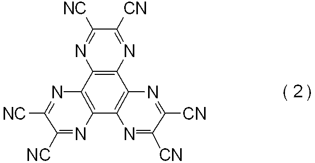
- the acceptor organic substance has the chemical formula (2)
- the electron injecting and transporting layer may contain a donor impurity.
- the cathode may include a layer of an oxide transparent conductive film material.
- the organic EL device of the present invention has at least a cathode, a cathode buffer layer made of the HAT derivative, an electron injecting and transporting layer, and a light emitting layer in this order from the substrate side, whereby oxygen and / or moisture adsorbed on the cathode Prevents the electron injection / transport performance of the electron injection / transport layer from being impaired, ensures the supply of electrons to the light emitting layer, reduces the drive voltage of the organic EL element, and gives the same current density as the drive time elapses It offers the significant advantage of preventing an increase in drive voltage.
- the organic EL layer can be thickened by the thickness of the cathode buffer layer without causing an increase in voltage, the occurrence of current leakage and pixel defects is suppressed, and the organic EL element is suppressed. It is possible to improve the quality and manufacturing yield of the product.
- FIG. 1 is a schematic view showing an organic EL device of the present invention.
- FIG. 2 is a graph showing current-voltage characteristics of the organic EL elements of Examples and Comparative Examples.
- the organic EL device of the present invention comprises a substrate, a cathode, an anode, an organic EL layer provided between the cathode and the anode, the cathode is in direct contact with the substrate, and the organic EL layer is directly on the cathode.
- a cathode buffer layer made of an acceptor organic material, an electron injecting and transporting layer, and a light emitting layer in this order, wherein the acceptor organic material has the chemical formula (1)
- each R is independently a hydrogen atom, a hydrocarbon group having 1 to 10 carbon atoms, a halogen, an alkoxy group, an arylamino group, an ester group, an amide group, an aromatic hydrocarbon group, a heterocyclic group Selected from the group consisting of a group, a nitro group, and a nitrile (—CN) group) It consists of the hexaazatriphenylene (HAT) derivative
- HAT hexaazatriphenylene
- FIG. 1 shows an example of the configuration of the organic EL element of the present invention.
- a cathode 120, an organic EL layer 130, and an anode 140 are stacked on a substrate 110.
- the organic EL layer 130 includes, in order from the cathode 120 side, a cathode buffer layer 131, an electron.
- the injection transport layer 132, the light emitting layer 133, the hole transport layer 134, the hole injection transport layer 135, and the anode buffer layer 136 are included.
- the hole transport layer 134, the hole injection transport layer 135, and the anode buffer layer 136 may be optionally provided.
- FIG. 1 an example in which the cathode 120 includes a reflective layer 121 and a transparent layer 122 is shown.
- the layer structure of the organic EL layer 130 satisfies the condition that the cathode buffer layer 131 is in direct contact with the cathode 120 and the electron injection / transport layer 132 and the light emitting layer 133 are laminated on the cathode buffer layer 131 in this order.
- an electron transport layer may optionally exist between the electron injection transport layer 132 and the light emitting layer 133.
- the following structure can be adopted.
- Cathode buffer layer / electron injection transport layer / light emitting layer (2) Cathode buffer layer / electron injection transport layer / light emitting layer / hole injection transport layer (3) Cathode buffer layer / electron injection transport layer / electron transport layer / Light emitting layer / hole injection transport layer (4) Cathode buffer layer / electron injection transport layer / light emitting layer / hole transport layer / hole injection transport layer (5) Cathode buffer layer / electron injection transport layer / electron transport layer / light emission Layer / hole transport layer / hole injection transport layer (in the above structure, the leftmost cathode buffer layer 131 is in direct contact with the cathode 120 and the rightmost layer is in direct contact with the anode 140)
- At least one of the cathode 120 and the anode 140 is light transmissive. Both the cathode 120 and the anode 140 may be light transmissive. Either the cathode 120 or the anode 140 can be selected depending on the intended application.
- the substrate 110 As the substrate 110 , a glass substrate is usually used. Alternatively, the substrate 110 is made of polyamide; polycarbonate; polyethylene terephthalate, polyethylene naphthalate, polybutylene terephthalate, poly-1,4-cyclohexanedimethylene terephthalate, polyethylene-1,2-diphenoxyethane-4,4′-dicarboxy.
- Polyester resins such as rate and polybutylene terephthalate; polystyrene; polyolefins such as polyethylene, polypropylene and polymethylpentene; acrylate resin systems such as polymethyl methacrylate; polysulfone; polyethersulfone; polyetherketone; polyetherimide; polyoxyethylene; It can also be formed from a polymer material such as norbornene resin.
- the substrate 110 may be rigid or flexible.
- the substrate 110 may be formed using a semiconductor such as silicon or an optically opaque material such as ceramic.
- the cathode 120 may be light reflective or light transmissive, provided that either the cathode 120 or the anode 140 is light transmissive.
- the cathode 120 may be composed of a reflective layer 121 and a transparent layer 122 as shown in FIG. At this time, it is desirable to adopt a configuration in which the reflective layer 121 is in contact with the substrate 110 and the transparent layer 122 is in contact with the organic EL layer 130.
- the reflective layer 121 can be formed using a high reflectivity metal, a high reflectivity amorphous alloy, or a high reflectivity microcrystalline alloy.
- High reflectivity metals include Al, Ag, Ta, Zn, Mo, W, Ni, Cr, and the like.
- High reflectivity amorphous alloys include NiP, NiB, CrP, CrB, and the like.
- High reflectivity microcrystalline alloys include NiAl, silver alloys and the like.
- the transparent layer 122 can be formed using a TCO material such as ITO, IZO, IWO, or AZO (Al-doped zinc oxide).
- the cathode 120 can be composed of a light transmissive layer and a charge injection metal layer.
- the light transmissive layer in order to smoothly inject electrons into the organic EL layer 130, it is desirable that the light transmissive layer is in contact with the substrate 110 and the electron injecting metal layer is in contact with the organic EL layer 130.
- the light transmissive layer can be formed using the TCO material described above.
- the electron injection metal layer can be formed using a metal, an alloy, an electrically conductive compound, and a mixture thereof having a small work function (4.0 eV or less). Specific examples of materials that can be used include sodium, sodium-potassium alloy, magnesium, lithium, magnesium-silver alloy, aluminum / aluminum oxide, aluminum-lithium alloy, indium, rare earth metals, and the like.
- the cathode 120 may be composed of only one of the electron injection metal layer and the light transmissive layer described above.
- the cathode 120 can be produced by forming a thin film of the above-described material using any means known in the art such as vapor deposition and sputtering.
- the cathode buffer layer 131 is the outermost layer on the cathode side of the organic EL layer 130 and is in contact with the cathode 120 and the electron injection / transport layer 132.
- the cathode buffer layer has the chemical formula (1)
- the cathode buffer layer 131 has the chemical formula (2)
- the cathode buffer layer 131 may have a thickness of 5 to 200 nm.
- the HAT derivative represented by the chemical formula (1) has a high electron accepting property and a deep LUMO. Therefore, an electron injection barrier is not formed between the cathode 131 and the cathode buffer layer 131 formed from the HAT derivative. Therefore, electrons can be extracted from the cathode 120 and transported toward the electron injecting and transporting layer 132 in the absence or extremely low voltage drop.
- the bulk conductivity of the HAT derivative is equal to or higher than that of a generally used charge transport material, the bulk voltage drop (voltage drop when electrons pass through the cathode buffer layer 131) is also high. Can be very low.
- the HAT derivative is stable to oxygen and moisture, and the electron injecting and transporting ability is not easily lowered by exposure to oxygen and / or moisture.
- the crystallinity of the HAT derivative after film formation is higher than that of a general amorphous organic material.
- the high crystallinity of the HAT derivative blocks oxygen and moisture adsorbed on the underlying layer (ie, the cathode 120) from passing through the layer formed thereon (ie, the electron injection / transport layer 132). The effect to do.
- the electron injection / transport layer 132 is doped with a donor impurity, electrons move from the cathode buffer layer 131 to the electron injection / transport layer 132 with a very low voltage drop.
- the film thickness of the organic EL layer 130 can be increased by the amount, the generation of pixel defects and line defects due to a short circuit between the cathode 120 and the anode 140 can be suppressed, thereby improving the quality of the organic EL element.
- the manufacturing yield can be improved.
- the electron injection / transport layer 132 is a layer located between the cathode buffer layer 131 and the light emitting layer 133.
- the electron injecting and transporting layer 132 includes 2- (4-biphenylyl) -5- (4-t-butylphenyl) -1,3,4-oxadiazole (PBD), 1,3,5-tris (4-t Oxadiazole derivatives such as -butylphenyl-1,3,4-oxadiazolyl) benzene (TPOB); 3-phenyl-4- (1'-naphthyl) -5-phenyl-1,2,4-triazole (TAZ) Triazine derivatives; phenylquinoxalines; 5,5′-bis (dimesitylboryl) -2,2′-bithiophene (BMB-2T), 5,5′-bis (dimesitylboryl) -2,2 ′ : 5'2'- thiophene
- donor impurities such as alkali metals such as Li, Na, K, and Cs, alkali metal halides such as LiF, NaF, KF, and CsF, or alkali metal carbonates such as Cs 2 CO 3 are included in the host material. May be doped to form the electron injecting and transporting layer 132.
- the aforementioned electron injecting and transporting material can be used as a host material. Electron migration from the cathode buffer layer 131 can be promoted by doping with donor impurities.
- the electron transport layer (not shown) is a layer that may optionally be provided between the electron injection transport layer 132 and the light emitting layer 133 in order to adjust the amount of electrons supplied to the light emitting layer 133.
- the electron transport layer can be formed using the electron injection transport material described above.
- the electron-injecting / transporting layer 132 is doped with a donor impurity, it is possible to avoid adverse effects such as quenching due to diffusion of the donor-type impurity in the light-emitting layer 133 by not doping the electron-transporting layer with the donor impurity.
- the electron transport layer may be formed of the same material as the host material of the electron injection transport layer 132.
- the light emitting layer 133 is a layer that emits light by recombining electrons injected from the cathode 120 and holes injected from the anode 140.
- the material of the light emitting layer 133 can be selected according to a desired color tone of light emission. For example, in order to obtain light emission from blue to blue-green, the light-emitting layer 133 is formed using a fluorescent brightener such as benzothiazole, benzimidazole, and benzoxazole, a styrylbenzene compound, an aromatic dimethylidene compound, and the like. Is possible.
- the light-emitting layer 133 may be formed by using the above-described material as a host material and adding a dopant thereto.
- Materials that can be used as dopants include, for example, perylene (blue), which is known for use as a laser dye.
- the hole injecting and transporting layer 135 in the present invention is a layer that may be optionally provided in order to promote the supply of holes to the light emitting layer 133.
- the hole injection / transport layer 135 can be formed using a hole injection / transport material generally used in an organic EL element or a p-type organic semiconductor material used in an organic TFT.
- Examples of the hole injection / transport material include 4,4′-bis ⁇ N- (1-naphthyl) -N-phenylamino ⁇ biphenyl (NPB), 2,2 ′, 7,7′-tetrakis ( N, N-diphenylamino) -9,9′-spirobifluorene (Spiro-TAD), tri (p-terphenyl-4-yl) amine (p-TTA), 1,3,5-tris [4- (3-methylphenylphenylamino) phenyl] benzene (m-MTDAPB), 4,4 ′, 4 ′′ -tris (N-carbazolyl) -triphenylamine (TCTA), etc.
- p-type organic semiconductor that can be used Materials include pentacene, naphthacene, ⁇ , ⁇ -dihexyl-6-thiophene and the like.
- the hole injecting and transporting layer 135 is formed by doping an acceptor impurity such as tetrafluorotetracyano-quinodimethane (F 4 -TCNQ), FeCl 3 , MoO 3 , V 2 O 5 in the host material. May be.
- acceptor impurity such as tetrafluorotetracyano-quinodimethane (F 4 -TCNQ), FeCl 3 , MoO 3 , V 2 O 5
- F 4 -TCNQ tetrafluorotetracyano-quinodimethane
- the hole transport layer 134 is a layer that may be optionally provided between the hole injection transport layer 135 and the light emitting layer 133 in order to adjust the amount of holes supplied to the light emitting layer 133.
- the hole injection layer 134 is used as a hole injection transport material in an organic EL element or a p-type organic semiconductor material in an organic TFT, such as a material having a triarylamine partial structure, a carbazole partial structure, or an oxadiazole partial structure. Can be formed using any known material.
- the HOMO level of the material forming the hole transport layer 134 is close to the HOMO level of the material forming the light emitting layer 133.
- the hole injection / transport material for forming the hole injection / transport layer 135 and the p-type organic semiconductor material, particularly NPB, spiro-TAD, p-TTA, TCTA, etc. are used to transport the hole.
- Layer 134 can be formed.
- the hole-injecting and transporting layer 135 when the hole-injecting and transporting layer 135 is doped with an acceptor impurity, by not doping the hole-transporting layer 134 with an acceptor impurity, the acceptor impurity is diffused into the light-emitting layer 133 and has an adverse effect such as quenching. You can avoid that.
- the hole transport layer may be formed of the same material as the host material of the hole injection transport layer 135.
- the anode buffer layer 136 is a layer that may be optionally provided in order to mitigate damage received by layers below the hole injection transport layer 135 when the anode 140 is formed.
- the anode buffer layer 136 can be formed using a material such as MgAg or MoO 3 , for example.
- Each of the above-described layers constituting the organic EL layer 130 can be formed using any means known in the art such as vapor deposition (resistance heating or electron beam heating).
- the anode 140 may be light reflective or light transmissive, provided that either the cathode 120 or the anode 140 is light transmissive.
- the anode 140 can be formed using the TCO material described above.
- a TCO material layer and a metal material thin film having a film thickness of about 50 nm or less
- a stacked body may be used as the anode 140.
- an auxiliary electrode (not shown) connected to the anode 140 may be provided in parallel with the anode 140 made of a TCO material.
- the auxiliary electrode can be formed using a low-resistance metal material.
- the anode 140 when the anode 140 is made light reflective, a laminate of a transparent layer and a reflective layer made of a TCO material can be used as the anode 140.
- a laminate of a transparent layer and a reflective layer made of a TCO material can be used as the anode 140.
- the reflective layer can be formed using a material similar to that of the reflective layer 121 in the cathode 120.
- the anode 140 can be produced by forming a thin film of the above-described material using any means known in the art such as vapor deposition and sputtering.
- Example 1 In this embodiment, a cathode 120 made of Ag and IZO, a cathode buffer layer 131, an electron injection transport layer 132, a light emitting layer 133, a hole transport layer 134, a hole injection transport layer 135, and an anode buffer layer 136 are formed on a substrate 110.
- This is an example of an organic EL element in which an anode 140 and an anode 140 are sequentially formed.
- An Ag film having a film thickness of 100 nm was formed on a glass substrate 110 (length 50 mm ⁇ width 50 mm ⁇ thickness 0.7 mm; Corning 1737 glass) by using a DC magnetron sputtering method. Furthermore, on the upper surface of the Ag film, a DC magnetron sputtering method (target: In 2 O 3 +10 wt% ZnO, discharge gas: Ar + 0.5% O 2 , discharge pressure: 0.3 Pa, discharge power: 1.45 W / cm 2 , An IZO film having a film thickness of 110 nm was formed at a substrate conveyance speed of 162 mm / min.
- the laminated body of the Ag film and the IZO film is processed into a stripe shape having a width of 2 mm by a photolithography method, thereby forming the reflective layer 121 having a width of 2 mm and the transparent layer 122 having a width of 2 mm.
- the organic EL layer 130 was formed on the cathode 120 using a resistance heating vapor deposition method.
- HAT-CN having a thickness of 20 nm was deposited to form the cathode buffer layer 131.
- tris (8-hydroxyquinolinato) aluminum (Alq 3 ) and Li were co-evaporated to co-evaporate so that the molar ratio of Alq 3 and Li was equal to form an electron injecting and transporting layer 132 having a thickness of 10 nm.
- Alq 3 and Li in the electron injecting and transporting layer 132 were equimolar.
- [4,4 ′, 4 ′′ -tris (3-methylphenylphenylamino) -triphenylamine (m-MTDATA) and F 4 -TCNQ are co-evaporated to form a hole injection transport layer having a thickness of 60 nm.
- the film thickness ratio of m-MTDATA and F 4 -TCNQ was set to 100: 3.
- MoO 3 molybdenum trioxide
- the stacked body on which the organic EL layer 130 was formed was moved to the opposed target sputtering apparatus without breaking the vacuum.
- IZO was deposited through a metal mask to form a stripe-shaped anode 140 having a thickness of 200 nm and a width of 2 mm, whereby the organic EL element 100 was obtained.
- the extending direction of the stripe of the anode 140 was set to a direction orthogonal to the extending direction of the stripe of the cathode 120.
- the organic EL element 100 was moved to the plasma CVD apparatus without breaking the vacuum.
- SiO 2 N 0.3 was deposited using a plasma CVD method, and a passivation layer (not shown) having a thickness of 3000 nm was formed so as to cover the organic EL element 100.
- the pressure in the apparatus (that is, the total pressure of the gas) is 100 Pa
- RF power having a frequency of 13.56 MHz and an output of 0.6 kW is applied as plasma generation power
- SiO 2 N 0 at a rate of 300 nm / min. .3 was deposited.
- Example 2 The procedure of Example 1 was repeated to produce an organic EL device, except that the thickness of the cathode buffer layer 131 was changed to 50 nm.
- Example 2 Except that the cathode buffer layer 131 was not formed, the procedure of Example 1 was repeated to produce an organic EL device.
- FIG. 2 shows the current-voltage characteristics of the obtained organic EL element.
- FIG. 2 shows that the voltages of the organic EL elements of Examples 1 and 2 of the present invention having a cathode buffer layer made of HAT-CN when compared at the same current density value are those of the comparative example having no cathode buffer layer. It shows that it is lower than the voltage of the element.
- the voltage of the element of Example 1 is 0.5 V lower than the voltage of the element of the comparative example.
- the voltage of the element of Example 2 having a thicker cathode buffer layer than that of Example 1 was 0.2 V higher than the voltage of the element of Example 1, but 0.3 V lower than the voltage of the element of Comparative Example. .
- the organic EL elements of Examples 1 and 2 and the comparative example were continuously driven at a current density of 0.04 A / cm 2 for 800 hours.
- the voltage giving a current density of 0.01 A / cm 2 after continuous driving increased by 0.8 V compared to the initial voltage.
- the voltage increase after continuous driving remained at 0.3V.
- the drive voltage is reduced and the drive voltage is prevented from being increased to give the same current density as the drive time elapses.
- the thickness of the organic EL layer can be increased by the thickness of the cathode buffer layer without increasing the voltage, current leakage and pixel defects can be suppressed. Therefore, it is considered possible to improve the quality and manufacturing yield of the organic EL element.
Landscapes
- Physics & Mathematics (AREA)
- Optics & Photonics (AREA)
- Spectroscopy & Molecular Physics (AREA)
- Chemical & Material Sciences (AREA)
- Engineering & Computer Science (AREA)
- Materials Engineering (AREA)
- Electroluminescent Light Sources (AREA)
- Nitrogen Condensed Heterocyclic Rings (AREA)
Abstract
Description
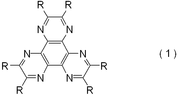
で示されるヘキサアザトリフェニレン誘導体からなることを特徴とする。ここで、アクセプター性有機物は、化学式(2)
110 基板
120 陰極
121 反射層
122 透明層
130 有機EL層
131 陰極バッファ層
132 電子注入輸送層
133 発光層
134 正孔輸送層
135 正孔注入輸送層
136 陽極バッファ層
140 陽極
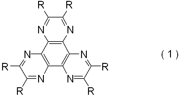
で示されるヘキサアザトリフェニレン(HAT)誘導体からなることを特徴とする。
(1)陰極バッファ層/電子注入輸送層/発光層
(2)陰極バッファ層/電子注入輸送層/発光層/正孔注入輸送層
(3)陰極バッファ層/電子注入輸送層/電子輸送層/発光層/正孔注入輸送層
(4)陰極バッファ層/電子注入輸送層/発光層/正孔輸送層/正孔注入輸送層
(5)陰極バッファ層/電子注入輸送層/電子輸送層/発光層/正孔輸送層/正孔注入輸送層
(上記構造において、左端の陰極バッファ層131は陰極120に直接接触しており、右端の層は陽極140に直接接触する)
基板110としては、通常、ガラス基板が用いられる。あるいはまた、基板110を、ポリアミド;ポリカーボネート;ポリエチレンテレフタレート、ポリエチレンナフタレート、ポリブチレンテレフタレート、ポリ-1,4-シクロヘキサンジメチレンテレフタレート、ポリエチレン-1,2-ジフェノキシエタン-4,4’-ジカルボキシレート、ポリブチレンテレフタレートなどのポリエステル樹脂;ポリスチレン;ポリエチレン、ポリプロピレン、ポリメチルペンテンなどのポリオレフィン;ポリメチルメタクリレート等のアクリレート樹脂系;ポリスルホン;ポリエーテルスルホン;ポリエーテルケトン;ポリエーテルイミド;ポリオキシエチレン;ノルボルネン樹脂などの高分子材料から形成することもできる。高分子材料を用いる場合、基板110は剛直であっても可撓性であってもよい。あるいはまた、有機EL層130の発光を基板110を通して外部へと取り出さない場合、シリコンなどの半導体、またはセラミックのような光学的に不透明な材料を用いて基板110を形成してもよい。
陰極120は、陰極120または陽極140のいずれか一方が光透過性であることを条件として、光反射性であっても、光透過性であってもよい。
陰極バッファ層131は、有機EL層130の陰極側の最外層であり、陰極120と電子注入輸送層132と接触する。陰極バッファ層は、化学式(1)


電子注入輸送層132は、陰極バッファ層131と発光層133との間に位置する層である。電子注入輸送層132は、2-(4-ビフェニリル)-5-(4-t-ブチルフェニル)-1,3,4-オキサジアゾール(PBD)、1,3,5-トリス(4-t-ブチルフェニル-1,3,4-オキサジアゾリル)ベンゼン(TPOB)のようなオキサジアゾール誘導体;3-フェニル-4-(1’-ナフチル)-5-フェニル-1,2,4-トリアゾール(TAZ)のようなトリアゾール誘導体;トリアジン誘導体;フェニルキノキサリン類;5,5’-ビス(ジメシチルボリル)-2,2’-ビチオフェン(BMB-2T)、5,5’-ビス(ジメシチルボリル)-2,2’:5’2’-ターチオフェン(BMB-3T)のようなチオフェン誘導体;アルミニウムトリス(8-キノリノラート)(Alq3)のようなアルミニウム錯体などの電子注入輸送材料を用いて形成することができる。
電子輸送層(不図示)は、発光層133への電子の供給量を調整するために、電子注入輸送層132と発光層133との間に任意選択的に設けてもよい層である。電子輸送層は、前述の電子注入輸送材料を用いて形成することができる。特に電子注入輸送層132にドナー不純物がドープされている場合、電子輸送層にドナー不純物がドープしないことによって、発光層133にドナー性不純物が拡散して消光などの悪影響を及ぼすことを回避できる。この際、電子輸送層を、電子注入輸送層132のホスト材料と同一の材料で形成してもよい。
発光層133は、陰極120から注入される電子と、陽極140から注入される正孔とを再結合させ、発光を行う層である。発光層133の材料は、所望する発光の色調に応じて選択することが可能である。たとえば青色から青緑色の発光を得るためには、ベンゾチアゾール系、ベンゾイミダゾール系、ベンゾオキサゾール系などの蛍光増白剤、スチリルベンゼン系化合物、芳香族ジメチリデイン系化合物などを用いて発光層133を形成することが可能である。あるいはまた、前述の材料をホスト材料として用い、これにドーパントを添加することによって、発光層133を形成してもよい。ドーパントとして用いることができる材料は、たとえばレーザ色素としての使用が知られているペリレン(青色)などを含む。
本発明における正孔注入輸送層135は、発光層133への正孔の供給を促進するために任意選択的に設けてもよい層である。正孔注入輸送層135は、一般的に有機EL素子で用いられている正孔注入輸送材料、または有機TFTで用いられるp型有機半導体材料を用いて形成することができる。用いることができる正孔注入輸送材料は、たとえば、4,4’-ビス{N-(1-ナフチル)-N-フェニルアミノ}ビフェニル(NPB)、2,2’,7,7’-テトラキス(N,N-ジフェニルアミノ)-9,9’-スピロビフルオレン(Spiro-TAD)、トリ(p-ターフェニル-4-イル)アミン(p-TTA)、1,3,5-トリス[4-(3-メチルフェニルフェニルアミノ)フェニル]ベンゼン(m-MTDAPB)、4,4’,4”-トリス(N-カルバゾリル)-トリフェニルアミン(TCTA)などを含む。用いることができるp型有機半導体材料は、ペンタセン、ナフタセン、α,ω-ジヘキシル-6-チオフェンなどを含む。
正孔輸送層134は、発光層133への正孔の供給量を調整するために、正孔注入輸送層135と発光層133との間に任意選択的に設けてもよい層である。正孔注入層134は、トリアリールアミン部分構造、カルバゾール部分構造またはオキサジアゾール部分構造を有する材料などの、有機EL素子における正孔注入輸送材料または有機TFTにおけるp型有機半導体材料として使用することが知られている任意の材料を用いて形成することができる。発光層133への正孔注入性の観点から、正孔輸送層134を形成する材料のHOMO準位を、発光層133を形成する材料のHOMO準位に接近させることが望ましい。具体的には、前述の正孔注入輸送層135を形成するための正孔注入輸送材料およびp型有機半導体材料、特にNPB、spiro-TAD、p-TTA、TCTAなどを用いて、正孔輸送層134を形成することができる。特に正孔注入輸送層135にアクセプター性不純物がドープされている場合、正孔輸送層134にアクセプター性不純物をドープしないことによって、発光層133にアクセプター性不純物が拡散して消光などの悪影響を及ぼすことを回避できる。この際、正孔輸送層を、正孔注入輸送層135のホスト材料と同一の材料で形成してもよい。
陽極バッファ層136は、陽極140の形成時に正孔注入輸送層135以下の層が受けるダメージを緩和するために、任意選択的に設けてもよい層である。陽極バッファ層136は、たとえば、MgAg、MoO3などの材料を用いて形成することができる。
陽極140は、陰極120または陽極140のいずれか一方が光透過性であることを条件として、光反射性であっても、光透過性であってもよい。
本実施例は、基板110上に、AgおよびIZOからなる陰極120、陰極バッファ層131、電子注入輸送層132、発光層133、正孔輸送層134、正孔注入輸送層135、陽極バッファ層136および陽極140を順次形成されている有機EL素子の例である。
陰極バッファ層131の膜厚を50nmに変更したことを除いて、実施例1の手順を繰り返して、有機EL素子を作製した。
陰極バッファ層131を形成しなかったことを除いて、実施例1の手順を繰り返して、有機EL素子を作製した。
得られた有機EL素子の電流-電圧特性を図2に示す。図2は、同一電流密度値で比較した場合に、HAT-CNからなる陰極バッファ層をもつ本発明の実施例1および2の有機EL素子の電圧が、陰極バッファ層をもたない比較例の素子の電圧よりも低いことを示している。たとえば、0.01A/cm2の電流密度を与える電圧を比較すると、実施例1の素子の電圧は、比較例の素子の電圧よりも0.5V低い。また、実施例1に比べて陰極バッファ層が厚い実施例2の素子の電圧も、実施例1の素子の電圧よりも0.2V上昇したものの、比較例の素子の電圧よりも0.3V低い。
Claims (4)
- 基板と、陰極と、陽極と、陰極および陽極の間に設けられた有機EL層からなる有機EL素子であって、陰極が基板に直接接触しており、有機EL層が、陰極に直接接触し、およびアクセプター性有機物からなる陰極バッファ層、電子注入輸送層、ならびに発光層をこの順に含み、前記アクセプター性有機物が、化学式(1)

で示されるヘキサアザトリフェニレン誘導体からなることを特徴とする有機EL素子。 - 前記アクセプター性有機物が、化学式(2)

- 前記電子注入輸送層が、ドナー性不純物を含有することを特徴とする請求項1に記載の有機EL素子。
- 前記陰極が、透明導電性酸化物材料の層を含むことを特徴とする請求項1に記載の有機EL素子。
Priority Applications (6)
| Application Number | Priority Date | Filing Date | Title |
|---|---|---|---|
| US12/734,549 US20120280214A1 (en) | 2008-12-25 | 2008-12-25 | Organic el element having cathode buffer layer |
| JP2010513571A JPWO2010073348A1 (ja) | 2008-12-25 | 2008-12-25 | 陰極バッファ層を有する有機el素子 |
| KR1020107008990A KR20100108507A (ko) | 2008-12-25 | 2008-12-25 | 음극 버퍼층을 가지는 유기 el 소자 |
| CN200880115185A CN101855741A (zh) | 2008-12-25 | 2008-12-25 | 具有阴极缓冲层的有机el元件 |
| PCT/JP2008/073638 WO2010073348A1 (ja) | 2008-12-25 | 2008-12-25 | 陰極バッファ層を有する有機el素子 |
| TW098144480A TW201041440A (en) | 2008-12-25 | 2009-12-23 | Organic EL element having cathode buffer layer |
Applications Claiming Priority (1)
| Application Number | Priority Date | Filing Date | Title |
|---|---|---|---|
| PCT/JP2008/073638 WO2010073348A1 (ja) | 2008-12-25 | 2008-12-25 | 陰極バッファ層を有する有機el素子 |
Publications (1)
| Publication Number | Publication Date |
|---|---|
| WO2010073348A1 true WO2010073348A1 (ja) | 2010-07-01 |
Family
ID=42287016
Family Applications (1)
| Application Number | Title | Priority Date | Filing Date |
|---|---|---|---|
| PCT/JP2008/073638 Ceased WO2010073348A1 (ja) | 2008-12-25 | 2008-12-25 | 陰極バッファ層を有する有機el素子 |
Country Status (6)
| Country | Link |
|---|---|
| US (1) | US20120280214A1 (ja) |
| JP (1) | JPWO2010073348A1 (ja) |
| KR (1) | KR20100108507A (ja) |
| CN (1) | CN101855741A (ja) |
| TW (1) | TW201041440A (ja) |
| WO (1) | WO2010073348A1 (ja) |
Cited By (9)
| Publication number | Priority date | Publication date | Assignee | Title |
|---|---|---|---|---|
| GB2485050A (en) * | 2010-10-25 | 2012-05-02 | Lg Display Co Ltd | Organic light emitting diode and method of fabricating the same |
| JP2012521087A (ja) * | 2009-03-17 | 2012-09-10 | エルジー・ケム・リミテッド | 有機発光素子およびその製造方法 |
| CN103081157A (zh) * | 2010-07-07 | 2013-05-01 | 株式会社Lg化学 | 包括封装结构的有机发光器件 |
| WO2013145667A1 (ja) * | 2012-03-29 | 2013-10-03 | ソニー株式会社 | 有機エレクトロルミネッセンス素子 |
| JP2013541217A (ja) * | 2010-10-15 | 2013-11-07 | ザ リージェンツ オブ ザ ユニヴァシティ オブ ミシガン | 光起電デバイスにおける感光層のエピタキシャル成長制御用材料 |
| JP2014167981A (ja) * | 2013-02-28 | 2014-09-11 | Nippon Hoso Kyokai <Nhk> | 有機エレクトロルミネッセンス素子およびその製造方法、表示装置 |
| WO2016035413A1 (ja) * | 2014-09-04 | 2016-03-10 | 株式会社Joled | 表示素子および表示装置ならびに電子機器 |
| JP2018503255A (ja) * | 2014-12-17 | 2018-02-01 | ノヴァレッド ゲーエムベーハー | 異なるマトリクス化合物を含んでいる電子伝達層を備えている有機発光ダイオード |
| JP2022186728A (ja) * | 2010-11-19 | 2022-12-15 | 株式会社半導体エネルギー研究所 | 照明装置 |
Families Citing this family (11)
| Publication number | Priority date | Publication date | Assignee | Title |
|---|---|---|---|---|
| CN102456839A (zh) * | 2010-10-21 | 2012-05-16 | 海洋王照明科技股份有限公司 | 一种有机电致发光器件及其制备方法 |
| TWI447982B (zh) * | 2011-05-24 | 2014-08-01 | Au Optronics Corp | 有機發光裝置 |
| KR102058238B1 (ko) * | 2013-09-02 | 2019-12-23 | 엘지디스플레이 주식회사 | 유기발광 다이오드 표시장치 |
| EP3489325B1 (en) | 2013-12-05 | 2020-06-10 | LG Display Co., Ltd. | Organic electroluminescent device |
| TWI601445B (zh) * | 2013-12-20 | 2017-10-01 | 友達光電股份有限公司 | 有機電激發光元件 |
| KR102445081B1 (ko) | 2015-09-24 | 2022-09-20 | 엘지디스플레이 주식회사 | 유기전계발광소자 |
| JP2018055937A (ja) * | 2016-09-28 | 2018-04-05 | 株式会社Joled | 有機el表示素子および有機el表示素子の製造方法 |
| KR102707375B1 (ko) * | 2016-11-30 | 2024-09-13 | 엘지디스플레이 주식회사 | 유기 발광 소자 및 그를 이용한 유기 발광 표시 장치 |
| CN112331806A (zh) * | 2017-05-24 | 2021-02-05 | 京东方科技集团股份有限公司 | 显示基板 |
| WO2022056792A1 (zh) * | 2020-09-17 | 2022-03-24 | 京东方科技集团股份有限公司 | 有机发光二极管和制备有机发光二极管的方法、显示装置及照明装置 |
| CN112614955A (zh) * | 2020-12-17 | 2021-04-06 | 北京维信诺科技有限公司 | 有机发光二极管和显示面板及制备方法、显示装置 |
Citations (4)
| Publication number | Priority date | Publication date | Assignee | Title |
|---|---|---|---|---|
| JP2001143871A (ja) * | 1999-11-12 | 2001-05-25 | Canon Inc | 有機発光素子 |
| JP2002100477A (ja) * | 2000-09-20 | 2002-04-05 | Kyocera Corp | 有機エレクトロルミネッセンス素子 |
| WO2007005325A1 (en) * | 2005-06-29 | 2007-01-11 | Eastman Kodak Company | Broadband light tandem oled display |
| WO2007130047A1 (en) * | 2006-05-08 | 2007-11-15 | Eastman Kodak Company | Oled electron-injecting layer |
Family Cites Families (4)
| Publication number | Priority date | Publication date | Assignee | Title |
|---|---|---|---|---|
| US5093698A (en) * | 1991-02-12 | 1992-03-03 | Kabushiki Kaisha Toshiba | Organic electroluminescent device |
| CN100397678C (zh) * | 2000-12-26 | 2008-06-25 | Lg化学株式会社 | 包含具有p-型半导体特性的有机化合物的电子器件 |
| US7629741B2 (en) * | 2005-05-06 | 2009-12-08 | Eastman Kodak Company | OLED electron-injecting layer |
| JP4804289B2 (ja) * | 2005-09-29 | 2011-11-02 | キヤノン株式会社 | 表示装置 |
-
2008
- 2008-12-25 US US12/734,549 patent/US20120280214A1/en not_active Abandoned
- 2008-12-25 WO PCT/JP2008/073638 patent/WO2010073348A1/ja not_active Ceased
- 2008-12-25 KR KR1020107008990A patent/KR20100108507A/ko not_active Ceased
- 2008-12-25 CN CN200880115185A patent/CN101855741A/zh active Pending
- 2008-12-25 JP JP2010513571A patent/JPWO2010073348A1/ja active Pending
-
2009
- 2009-12-23 TW TW098144480A patent/TW201041440A/zh unknown
Patent Citations (4)
| Publication number | Priority date | Publication date | Assignee | Title |
|---|---|---|---|---|
| JP2001143871A (ja) * | 1999-11-12 | 2001-05-25 | Canon Inc | 有機発光素子 |
| JP2002100477A (ja) * | 2000-09-20 | 2002-04-05 | Kyocera Corp | 有機エレクトロルミネッセンス素子 |
| WO2007005325A1 (en) * | 2005-06-29 | 2007-01-11 | Eastman Kodak Company | Broadband light tandem oled display |
| WO2007130047A1 (en) * | 2006-05-08 | 2007-11-15 | Eastman Kodak Company | Oled electron-injecting layer |
Cited By (14)
| Publication number | Priority date | Publication date | Assignee | Title |
|---|---|---|---|---|
| JP2012521087A (ja) * | 2009-03-17 | 2012-09-10 | エルジー・ケム・リミテッド | 有機発光素子およびその製造方法 |
| CN103081157A (zh) * | 2010-07-07 | 2013-05-01 | 株式会社Lg化学 | 包括封装结构的有机发光器件 |
| CN103081157B (zh) * | 2010-07-07 | 2017-07-25 | 乐金显示有限公司 | 包括封装结构的有机发光器件 |
| JP2013541217A (ja) * | 2010-10-15 | 2013-11-07 | ザ リージェンツ オブ ザ ユニヴァシティ オブ ミシガン | 光起電デバイスにおける感光層のエピタキシャル成長制御用材料 |
| GB2485050A (en) * | 2010-10-25 | 2012-05-02 | Lg Display Co Ltd | Organic light emitting diode and method of fabricating the same |
| JP2022186728A (ja) * | 2010-11-19 | 2022-12-15 | 株式会社半導体エネルギー研究所 | 照明装置 |
| JP7815365B2 (ja) | 2010-11-19 | 2026-02-17 | 株式会社半導体エネルギー研究所 | 照明装置 |
| JP2024167339A (ja) * | 2010-11-19 | 2024-12-03 | 株式会社半導体エネルギー研究所 | 照明装置 |
| WO2013145667A1 (ja) * | 2012-03-29 | 2013-10-03 | ソニー株式会社 | 有機エレクトロルミネッセンス素子 |
| US9978975B2 (en) | 2012-03-29 | 2018-05-22 | Joled Inc | Organic electroluminescence device |
| JP2014167981A (ja) * | 2013-02-28 | 2014-09-11 | Nippon Hoso Kyokai <Nhk> | 有機エレクトロルミネッセンス素子およびその製造方法、表示装置 |
| WO2016035413A1 (ja) * | 2014-09-04 | 2016-03-10 | 株式会社Joled | 表示素子および表示装置ならびに電子機器 |
| JPWO2016035413A1 (ja) * | 2014-09-04 | 2017-04-27 | 株式会社Joled | 表示素子および表示装置ならびに電子機器 |
| JP2018503255A (ja) * | 2014-12-17 | 2018-02-01 | ノヴァレッド ゲーエムベーハー | 異なるマトリクス化合物を含んでいる電子伝達層を備えている有機発光ダイオード |
Also Published As
| Publication number | Publication date |
|---|---|
| KR20100108507A (ko) | 2010-10-07 |
| TW201041440A (en) | 2010-11-16 |
| CN101855741A (zh) | 2010-10-06 |
| US20120280214A1 (en) | 2012-11-08 |
| JPWO2010073348A1 (ja) | 2012-05-31 |
Similar Documents
| Publication | Publication Date | Title |
|---|---|---|
| WO2010073348A1 (ja) | 陰極バッファ層を有する有機el素子 | |
| KR101345617B1 (ko) | 유기 일렉트로루미네센스 소자 | |
| JP5912977B2 (ja) | バッファ層を含む有機発光素子およびその製作方法 | |
| KR101199695B1 (ko) | 유기 이엘 소자 | |
| JP4736890B2 (ja) | 有機エレクトロルミネッセンス素子 | |
| KR101003130B1 (ko) | 유기 전계발광 소자 | |
| JP5333121B2 (ja) | 有機エレクトロルミネッセンス素子、その製造方法及び発光表示装置 | |
| US20110291156A1 (en) | Organic electroluminescent element | |
| US9859517B2 (en) | White organic light-emitting diode | |
| KR20090095022A (ko) | 백색 유기발광소자 | |
| JP5603254B2 (ja) | 有機発光素子およびその製作方法 | |
| CN102388477A (zh) | 有机电致发光元件及其制造方法 | |
| WO2009119591A1 (ja) | 有機エレクトロルミネッセンス素子 | |
| WO2011021280A1 (ja) | 有機エレクトロルミネッセンス素子およびその製造方法 | |
| Liu et al. | Inverted Tandem Phosphorescence Organic Light-Emitting Diodes Based on $\hbox {MoO} _ {3}/\hbox {Al/Cs} _ {2}\hbox {CO} _ {3} $ Charge Generation Unit | |
| WO2011049141A1 (ja) | 有機エレクトロルミネッセンス素子を用いた発光装置、およびその製造方法、ならびに該発光装置を備えた有機エレクトロルミネッセンス表示装置 |
Legal Events
| Date | Code | Title | Description |
|---|---|---|---|
| WWE | Wipo information: entry into national phase |
Ref document number: 200880115185.3 Country of ref document: CN |
|
| WWE | Wipo information: entry into national phase |
Ref document number: 2010513571 Country of ref document: JP |
|
| ENP | Entry into the national phase |
Ref document number: 20107008990 Country of ref document: KR Kind code of ref document: A |
|
| 121 | Ep: the epo has been informed by wipo that ep was designated in this application |
Ref document number: 08879144 Country of ref document: EP Kind code of ref document: A1 |
|
| WWE | Wipo information: entry into national phase |
Ref document number: 12734549 Country of ref document: US |
|
| NENP | Non-entry into the national phase |
Ref country code: DE |
|
| 122 | Ep: pct application non-entry in european phase |
Ref document number: 08879144 Country of ref document: EP Kind code of ref document: A1 |