WO2010071160A1 - アクティブマトリクス基板の製造方法、および、液晶表示装置の製造方法 - Google Patents
アクティブマトリクス基板の製造方法、および、液晶表示装置の製造方法 Download PDFInfo
- Publication number
- WO2010071160A1 WO2010071160A1 PCT/JP2009/070999 JP2009070999W WO2010071160A1 WO 2010071160 A1 WO2010071160 A1 WO 2010071160A1 JP 2009070999 W JP2009070999 W JP 2009070999W WO 2010071160 A1 WO2010071160 A1 WO 2010071160A1
- Authority
- WO
- WIPO (PCT)
- Prior art keywords
- layer
- signal line
- photosensitive resin
- electrode
- amorphous silicon
- Prior art date
- Legal status (The legal status is an assumption and is not a legal conclusion. Google has not performed a legal analysis and makes no representation as to the accuracy of the status listed.)
- Ceased
Links
Images














Classifications
-
- G—PHYSICS
- G02—OPTICS
- G02F—OPTICAL DEVICES OR ARRANGEMENTS FOR THE CONTROL OF LIGHT BY MODIFICATION OF THE OPTICAL PROPERTIES OF THE MEDIA OF THE ELEMENTS INVOLVED THEREIN; NON-LINEAR OPTICS; FREQUENCY-CHANGING OF LIGHT; OPTICAL LOGIC ELEMENTS; OPTICAL ANALOGUE/DIGITAL CONVERTERS
- G02F1/00—Devices or arrangements for the control of the intensity, colour, phase, polarisation or direction of light arriving from an independent light source, e.g. switching, gating or modulating; Non-linear optics
- G02F1/01—Devices or arrangements for the control of the intensity, colour, phase, polarisation or direction of light arriving from an independent light source, e.g. switching, gating or modulating; Non-linear optics for the control of the intensity, phase, polarisation or colour
- G02F1/13—Devices or arrangements for the control of the intensity, colour, phase, polarisation or direction of light arriving from an independent light source, e.g. switching, gating or modulating; Non-linear optics for the control of the intensity, phase, polarisation or colour based on liquid crystals, e.g. single liquid crystal display cells
- G02F1/133—Constructional arrangements; Operation of liquid crystal cells; Circuit arrangements
- G02F1/1333—Constructional arrangements; Manufacturing methods
- G02F1/1343—Electrodes
- G02F1/134309—Electrodes characterised by their geometrical arrangement
- G02F1/134363—Electrodes characterised by their geometrical arrangement for applying an electric field parallel to the substrate, i.e. in-plane switching [IPS]
-
- G—PHYSICS
- G02—OPTICS
- G02F—OPTICAL DEVICES OR ARRANGEMENTS FOR THE CONTROL OF LIGHT BY MODIFICATION OF THE OPTICAL PROPERTIES OF THE MEDIA OF THE ELEMENTS INVOLVED THEREIN; NON-LINEAR OPTICS; FREQUENCY-CHANGING OF LIGHT; OPTICAL LOGIC ELEMENTS; OPTICAL ANALOGUE/DIGITAL CONVERTERS
- G02F1/00—Devices or arrangements for the control of the intensity, colour, phase, polarisation or direction of light arriving from an independent light source, e.g. switching, gating or modulating; Non-linear optics
- G02F1/01—Devices or arrangements for the control of the intensity, colour, phase, polarisation or direction of light arriving from an independent light source, e.g. switching, gating or modulating; Non-linear optics for the control of the intensity, phase, polarisation or colour
- G02F1/13—Devices or arrangements for the control of the intensity, colour, phase, polarisation or direction of light arriving from an independent light source, e.g. switching, gating or modulating; Non-linear optics for the control of the intensity, phase, polarisation or colour based on liquid crystals, e.g. single liquid crystal display cells
- G02F1/133—Constructional arrangements; Operation of liquid crystal cells; Circuit arrangements
- G02F1/136—Liquid crystal cells structurally associated with a semi-conducting layer or substrate, e.g. cells forming part of an integrated circuit
- G02F1/1362—Active matrix addressed cells
- G02F1/136286—Wiring, e.g. gate line, drain line
-
- G—PHYSICS
- G02—OPTICS
- G02F—OPTICAL DEVICES OR ARRANGEMENTS FOR THE CONTROL OF LIGHT BY MODIFICATION OF THE OPTICAL PROPERTIES OF THE MEDIA OF THE ELEMENTS INVOLVED THEREIN; NON-LINEAR OPTICS; FREQUENCY-CHANGING OF LIGHT; OPTICAL LOGIC ELEMENTS; OPTICAL ANALOGUE/DIGITAL CONVERTERS
- G02F1/00—Devices or arrangements for the control of the intensity, colour, phase, polarisation or direction of light arriving from an independent light source, e.g. switching, gating or modulating; Non-linear optics
- G02F1/01—Devices or arrangements for the control of the intensity, colour, phase, polarisation or direction of light arriving from an independent light source, e.g. switching, gating or modulating; Non-linear optics for the control of the intensity, phase, polarisation or colour
- G02F1/13—Devices or arrangements for the control of the intensity, colour, phase, polarisation or direction of light arriving from an independent light source, e.g. switching, gating or modulating; Non-linear optics for the control of the intensity, phase, polarisation or colour based on liquid crystals, e.g. single liquid crystal display cells
- G02F1/133—Constructional arrangements; Operation of liquid crystal cells; Circuit arrangements
- G02F1/136—Liquid crystal cells structurally associated with a semi-conducting layer or substrate, e.g. cells forming part of an integrated circuit
- G02F1/1362—Active matrix addressed cells
- G02F1/1368—Active matrix addressed cells in which the switching element is a three-electrode device
-
- H—ELECTRICITY
- H10—SEMICONDUCTOR DEVICES; ELECTRIC SOLID-STATE DEVICES NOT OTHERWISE PROVIDED FOR
- H10D—INORGANIC ELECTRIC SEMICONDUCTOR DEVICES
- H10D30/00—Field-effect transistors [FET]
- H10D30/60—Insulated-gate field-effect transistors [IGFET]
- H10D30/67—Thin-film transistors [TFT]
- H10D30/6729—Thin-film transistors [TFT] characterised by the electrodes
- H10D30/6737—Thin-film transistors [TFT] characterised by the electrodes characterised by the electrode materials
-
- H—ELECTRICITY
- H10—SEMICONDUCTOR DEVICES; ELECTRIC SOLID-STATE DEVICES NOT OTHERWISE PROVIDED FOR
- H10D—INORGANIC ELECTRIC SEMICONDUCTOR DEVICES
- H10D30/00—Field-effect transistors [FET]
- H10D30/60—Insulated-gate field-effect transistors [IGFET]
- H10D30/67—Thin-film transistors [TFT]
- H10D30/6729—Thin-film transistors [TFT] characterised by the electrodes
- H10D30/6737—Thin-film transistors [TFT] characterised by the electrodes characterised by the electrode materials
- H10D30/6739—Conductor-insulator-semiconductor electrodes
-
- H—ELECTRICITY
- H10—SEMICONDUCTOR DEVICES; ELECTRIC SOLID-STATE DEVICES NOT OTHERWISE PROVIDED FOR
- H10D—INORGANIC ELECTRIC SEMICONDUCTOR DEVICES
- H10D30/00—Field-effect transistors [FET]
- H10D30/60—Insulated-gate field-effect transistors [IGFET]
- H10D30/67—Thin-film transistors [TFT]
- H10D30/674—Thin-film transistors [TFT] characterised by the active materials
- H10D30/6741—Group IV materials, e.g. germanium or silicon carbide
- H10D30/6743—Silicon
-
- H—ELECTRICITY
- H10—SEMICONDUCTOR DEVICES; ELECTRIC SOLID-STATE DEVICES NOT OTHERWISE PROVIDED FOR
- H10D—INORGANIC ELECTRIC SEMICONDUCTOR DEVICES
- H10D86/00—Integrated devices formed in or on insulating or conducting substrates, e.g. formed in silicon-on-insulator [SOI] substrates or on stainless steel or glass substrates
- H10D86/01—Manufacture or treatment
- H10D86/021—Manufacture or treatment of multiple TFTs
- H10D86/0231—Manufacture or treatment of multiple TFTs using masks, e.g. half-tone masks
-
- H—ELECTRICITY
- H10—SEMICONDUCTOR DEVICES; ELECTRIC SOLID-STATE DEVICES NOT OTHERWISE PROVIDED FOR
- H10D—INORGANIC ELECTRIC SEMICONDUCTOR DEVICES
- H10D86/00—Integrated devices formed in or on insulating or conducting substrates, e.g. formed in silicon-on-insulator [SOI] substrates or on stainless steel or glass substrates
- H10D86/40—Integrated devices formed in or on insulating or conducting substrates, e.g. formed in silicon-on-insulator [SOI] substrates or on stainless steel or glass substrates characterised by multiple TFTs
- H10D86/441—Interconnections, e.g. scanning lines
-
- H—ELECTRICITY
- H10—SEMICONDUCTOR DEVICES; ELECTRIC SOLID-STATE DEVICES NOT OTHERWISE PROVIDED FOR
- H10D—INORGANIC ELECTRIC SEMICONDUCTOR DEVICES
- H10D86/00—Integrated devices formed in or on insulating or conducting substrates, e.g. formed in silicon-on-insulator [SOI] substrates or on stainless steel or glass substrates
- H10D86/40—Integrated devices formed in or on insulating or conducting substrates, e.g. formed in silicon-on-insulator [SOI] substrates or on stainless steel or glass substrates characterised by multiple TFTs
- H10D86/60—Integrated devices formed in or on insulating or conducting substrates, e.g. formed in silicon-on-insulator [SOI] substrates or on stainless steel or glass substrates characterised by multiple TFTs wherein the TFTs are in active matrices
-
- G—PHYSICS
- G02—OPTICS
- G02F—OPTICAL DEVICES OR ARRANGEMENTS FOR THE CONTROL OF LIGHT BY MODIFICATION OF THE OPTICAL PROPERTIES OF THE MEDIA OF THE ELEMENTS INVOLVED THEREIN; NON-LINEAR OPTICS; FREQUENCY-CHANGING OF LIGHT; OPTICAL LOGIC ELEMENTS; OPTICAL ANALOGUE/DIGITAL CONVERTERS
- G02F1/00—Devices or arrangements for the control of the intensity, colour, phase, polarisation or direction of light arriving from an independent light source, e.g. switching, gating or modulating; Non-linear optics
- G02F1/01—Devices or arrangements for the control of the intensity, colour, phase, polarisation or direction of light arriving from an independent light source, e.g. switching, gating or modulating; Non-linear optics for the control of the intensity, phase, polarisation or colour
- G02F1/13—Devices or arrangements for the control of the intensity, colour, phase, polarisation or direction of light arriving from an independent light source, e.g. switching, gating or modulating; Non-linear optics for the control of the intensity, phase, polarisation or colour based on liquid crystals, e.g. single liquid crystal display cells
- G02F1/133—Constructional arrangements; Operation of liquid crystal cells; Circuit arrangements
- G02F1/136—Liquid crystal cells structurally associated with a semi-conducting layer or substrate, e.g. cells forming part of an integrated circuit
- G02F1/1362—Active matrix addressed cells
- G02F1/136286—Wiring, e.g. gate line, drain line
- G02F1/13629—Multilayer wirings
-
- G—PHYSICS
- G02—OPTICS
- G02F—OPTICAL DEVICES OR ARRANGEMENTS FOR THE CONTROL OF LIGHT BY MODIFICATION OF THE OPTICAL PROPERTIES OF THE MEDIA OF THE ELEMENTS INVOLVED THEREIN; NON-LINEAR OPTICS; FREQUENCY-CHANGING OF LIGHT; OPTICAL LOGIC ELEMENTS; OPTICAL ANALOGUE/DIGITAL CONVERTERS
- G02F1/00—Devices or arrangements for the control of the intensity, colour, phase, polarisation or direction of light arriving from an independent light source, e.g. switching, gating or modulating; Non-linear optics
- G02F1/01—Devices or arrangements for the control of the intensity, colour, phase, polarisation or direction of light arriving from an independent light source, e.g. switching, gating or modulating; Non-linear optics for the control of the intensity, phase, polarisation or colour
- G02F1/13—Devices or arrangements for the control of the intensity, colour, phase, polarisation or direction of light arriving from an independent light source, e.g. switching, gating or modulating; Non-linear optics for the control of the intensity, phase, polarisation or colour based on liquid crystals, e.g. single liquid crystal display cells
- G02F1/133—Constructional arrangements; Operation of liquid crystal cells; Circuit arrangements
- G02F1/136—Liquid crystal cells structurally associated with a semi-conducting layer or substrate, e.g. cells forming part of an integrated circuit
- G02F1/1362—Active matrix addressed cells
- G02F1/136286—Wiring, e.g. gate line, drain line
- G02F1/136295—Materials; Compositions; Manufacture processes
Definitions
- the present invention relates to an active matrix type liquid crystal display device having a transistor for each pixel, and a method of manufacturing an active matrix substrate provided in the liquid crystal display device.
- liquid crystal display device liquid crystal panel
- gate wirings gate wirings
- source wirings data signal lines
- liquid crystal display devices have been simultaneously increased in screen size and resolution in order to cope with an increase in display capacity.
- FIG. 33 is a perspective view showing a liquid crystal panel mounting means disclosed in Patent Document 7.
- FIG. A semiconductor integrated circuit chip 3 that supplies a drive signal to an electrode terminal 5 of a scanning signal line formed on one transparent insulating substrate, for example, a glass substrate 2, constituting the liquid crystal panel 1 is connected using a conductive adhesive.
- COG Chip-On-Glass
- a TCP film 4 based on a polyimide resin thin film and having a copper foil terminal plated with gold or solder includes a conductive medium in the electrode terminal 6 of the data signal line
- An electrical signal is supplied to the image display unit by a mounting means such as a TCP (Tape-Carrier-Package) method that is fixed by pressure contact with an appropriate adhesive.
- TCP Transmission-Carrier-Package
- Reference numerals 7 and 8 denote wiring paths that connect the pixels in the image display unit located almost at the center of the liquid crystal panel 1 and the electrode terminals 5 and 6 of the scanning signal lines and the data signal lines. It is not necessary to be made of the same conductive material as that in FIG.
- Reference numeral 9 denotes a counter glass substrate or a color filter substrate which is another transparent insulating substrate having a transparent conductive counter electrode common to all liquid crystal cells on the counter surface.
- FIG. 34 is an equivalent circuit diagram of an active liquid crystal display device in which the insulated gate transistor 10 is arranged for each pixel as a switching element.
- reference numeral 11 denotes a scanning signal line
- reference numeral 12 reference numeral 8 in FIG. 33
- reference numeral 13 denotes a liquid crystal cell
- the liquid crystal cell 13 is electrically connected. Is treated as a capacitive element.
- Elements drawn with solid lines are formed on one glass substrate 2 constituting the liquid crystal panel 1, and the counter electrode 14 common to all liquid crystal cells 13 drawn with dotted lines is the other glass substrate (color filter substrate). 9) on the main surface facing the glass substrate 2.
- an auxiliary storage capacitor for increasing the time constant of the liquid crystal cell 13 as a load A circuit device such as adding (auxiliary capacitor) 15 to the liquid crystal cell 13 in parallel is added.
- Reference numeral 16 denotes a storage capacitor line or a common electrode serving as a common bus for the storage capacitor 15.
- FIG. 35 is a cross-sectional view showing the main part of the image display part of the liquid crystal display device.
- the two glass substrates 2 and 9 constituting the liquid crystal panel 1 are made of spacer fibers such as resinous fibers, beads or columnar spacers formed on the color filter substrate 9 (both not shown).
- the gap (gap) is sealed with a sealing material made of an organic resin and a sealing material (both not shown) at the periphery of the glass substrate 9.
- the closed space is filled with liquid crystal 17.
- an organic thin film having a thickness of about 1 to 2 ⁇ m containing either or both of a dye and a pigment called a colored layer 18 is deposited on the closed space side of the glass substrate 9 to provide a color display function.
- the glass substrate 9 is also called a color filter (color filter abbreviation is CF) substrate.
- CF color filter abbreviation
- a polarizing plate 19 is attached to either the upper surface of the glass substrate 9, the lower surface of the glass substrate 2, or both surfaces, and the liquid crystal panel 1 functions as an electro-optical element.
- TN twisted nematic
- two polarizing plates 19 are usually required.
- a back light source is disposed as a light source, and white light is irradiated from below.
- the polyimide resin thin film 20 having a thickness of, for example, about 0.1 ⁇ m formed on the two glass substrates 2 and 9 in contact with the liquid crystal 17 is an alignment film for aligning liquid crystal molecules in a predetermined direction.
- Reference numeral 21 denotes a drain electrode (wiring) that connects the drain of the insulated gate transistor 10 and the transparent conductive pixel electrode 22, and is often formed simultaneously with the data signal line (source wiring) 12.
- the semiconductor layer 23 is located between the source electrode 12 and the drain electrode 21 and will be described in detail later.
- the production of the active matrix substrate 71 in which the scanning signal line, the data signal line, the insulated gate transistor as the switching element, and the pixel electrode are formed on the glass substrate 2 is performed a plurality of times using a photomask like a semiconductor integrated circuit.
- the photolithography process is essential. Although detailed details are omitted, as a result of streamlining the process of islanding the semiconductor layer and reducing the contact formation process to the scanning signal lines, the introduction of dry etching technology for photomasks that originally required about 7-8 sheets As a result, the number is reduced to 5 at the present time, which greatly contributes to the reduction of process costs.
- Patent Document 1 a manufacturing method that requires five photolithography steps in the production of the active matrix substrate 71 is common, but a manufacturing method that can further reduce the manufacturing cost is disclosed in Patent Document 1. ing.
- the four-mask process disclosed in Patent Document 1 will be described.
- This four-mask process is a process reduction technique or rationalization technique in which a halftone exposure technique is used to form an island formation process and a source / drain wiring process of a semiconductor layer including a channel with a single photomask.
- FIGS. 38 and 39 are the same as the line AA ′ (insulated gate type transistor region), the line BB ′ (electrode terminal region of the scanning signal line), and the line CC ′ (data signal) of FIG. It is sectional drawing which shows the manufacturing process in the electrode terminal area
- insulated gate transistors an etch stop type and a channel etch type, have been widely used.
- a channel-etched insulated gate transistor is shown.
- a glass substrate 2 having a thickness of about 0.5 to 1.1 mm as an insulating substrate having high heat resistance, chemical resistance and transparency For example, a first metal layer (metal for a scanning signal line) having a film thickness of about 0.1 to 0.3 ⁇ m is formed on one main surface of a product name 1737 manufactured by Corning using a vacuum film forming apparatus such as SPT (sputtering).
- the scanning signal line 11 that also serves as the gate electrode 11A and the storage capacitor line 16 are selectively formed by a fine processing technique.
- the material of the scanning signal line is selected by comprehensively considering heat resistance, chemical resistance, hydrofluoric acid resistance, and conductivity.
- a metal thin film layer such as Cr and Ta having high heat resistance or MoW alloy is used. The alloy thin film layer is used.
- the scanning signal line 11 is usually composed of one or more metal layers.
- a first silicon nitride (SiNx) layer 30 serving as a gate insulating layer is formed on the entire surface of the glass substrate 2 by using a PCVD (plasma sieve) device.
- the film is sequentially deposited with each film thickness of about 0.3-0.2-0.05 ⁇ m.
- a Ti thin film layer 34 as a heat resistant metal layer having a thickness of about 0.1 ⁇ m
- an Al thin film layer 35 as a low resistance metal layer having a thickness of about 0.3 ⁇ m
- a Ti thin film layer 36 is sequentially deposited as a buffer metal layer having a thickness of about 0.1 ⁇ m to form a source / drain wiring material.
- a data signal that also serves as a source electrode of an insulated gate transistor which is formed by stacking a heat-resistant metal layer 34A, a low-resistance metal layer 35A, and a buffer metal layer 36A so as to partially overlap with the gate electrode 11A by microfabrication technology.
- the line 12 and the drain electrode 21 of the insulated gate transistor configured by stacking the heat-resistant metal layer 34B, the low-resistance metal layer 35B, and the buffer metal layer 36B so as to partially overlap the gate electrode 11A are selectively used.
- a channel formation region 80B between the source and the drain hatchched line in FIG.
- the photosensitive resin patterns 80A and 80B are formed so that the film thickness of the portion) is 1.5 ⁇ m and the film thickness of the source / drain wiring formation regions 80A (12) and 80A (21) is 3 ⁇ m.
- the photosensitive resin patterns 80A and 80B reduce the light passing through the photomask in the source / drain wiring formation region 80A in black, that is, a Cr thin film, and in the channel formation region 80B in gray (halftone).
- a photomask in which a line-and-space Cr pattern having a width of about 0.5 to 1.5 ⁇ m is formed and white, that is, a Cr thin film is removed in other regions may be used.
- the line-and-space is not resolved because the resolving power of the exposure machine is insufficient, and it is possible to transmit about half of the photomask irradiation light from the lamp light source.
- photosensitive resin patterns 80A and 80B having a concave cross-sectional shape as shown in FIG. 38C can be obtained.
- the gray region may be formed of a metal layer having a different film thickness or transmittance, for example, a thin film of MoSi 2 instead of the slit.
- the photosensitive resin patterns 80A and 80B are used as a mask, as shown in FIGS. 36B and 38B, a Ti thin film layer 36, an Al thin film layer 35, a Ti thin film layer 34, and a second amorphous film.
- the photosensitive resin patterns 80A and 80B are reduced by 1.5 ⁇ m or more by ashing means such as oxygen plasma.
- the photosensitive resin pattern 80B disappears and the Ti thin film layer 36 in the channel forming region is exposed (not shown).
- the reduced photosensitive resin patterns 80C (12) and 80C (21) are left only in the source / drain wiring formation regions. it can.
- the Ti thin film layer 36, the Al thin film layer 35, the Ti thin film layer 34, and the second thin film between the source and drain wirings (channel formation region) are again formed.
- the amorphous silicon layer 33 and the first amorphous silicon layer 31 are sequentially etched, and the first amorphous silicon layer 31A is etched leaving about 0.05 to 0.1 ⁇ m.
- the source 33S and the drain 33D made of the second amorphous silicon layer are separated. Since the source / drain wirings 12 and 21 are formed by etching the metal layer and etching the first amorphous silicon layer 31A leaving about 0.05 to 0.1 ⁇ m.
- the resulting insulated gate transistor is called channel etch.
- the photosensitive resin pattern 80A is converted into a photosensitive resin pattern 80C having a reduced film thickness. Therefore, it is desirable to increase the anisotropy in order to suppress the change in pattern dimension.
- a reactive ion etching (IC) method, an ICP (Inductively Coupled Plasma) method having a high-density plasma source, and a TCP (Transfer Coupled Plasma) method are more desirable.
- a second SiNx layer having a thickness of about 0.3 ⁇ m is covered as a transparent insulating layer on the entire surface of the glass substrate 2. Then, a passivation insulating layer 37 is formed. As shown in FIGS. 37A and 39A, the scanning signal line 11 and the data signal line are formed on the drain electrode 21 and in a region outside the image display portion. Openings 62, 63, and 64 are formed in regions where 12 electrode terminals are formed, respectively.
- the passivation insulating layer 37 and the gate insulating layer 30 in the opening 63 are removed to expose a part 5 of the scanning signal line in the opening 63 and the passivation insulating layer 37 in the openings 62 and 64 is removed.
- a part of the drain electrode 21 and a part 6 of the data signal line are exposed.
- an opening 65 is formed on the storage capacitor line 16 to expose a part of the storage capacitor line 16.
- a transparent conductive layer having a film thickness of about 0.1 to 0.2 ⁇ m using a vacuum film forming apparatus such as SPT for example, ITO (Indium-Tin-Oxide) or IZO (Indium-Zinc-Oxide) or a mixture thereof.
- a transparent conductive pixel electrode 22 including an opening 62 is selectively formed on the passivation insulating layer 37 by a fine processing technique as shown in FIGS. Then, the active matrix substrate 71 is completed.
- the configuration of the storage capacitor 15 FIG. 34
- the drain electrode 21 and the storage capacitor line 16 are connected to the gate insulating layer 30 and the first amorphous layer. It is configured to overlap in a planar manner with the porous silicon layer 31A and the second amorphous silicon layer 33D (the downward slanted line portion 50 in FIG. 37A).
- transparent conductive electrode terminals 5A and 6A are selectively formed on the passivation insulating layer 37 including the openings 63 and 64.
- the refractory metal layer 34 is required to ensure electrical connection with the second amorphous silicon 33.
- a buffer metal layer 36 is required between the transparent conductive layer and the transparent conductive layer in order to avoid the battery effect in the alkaline solution.
- the source / drain wiring must have a three-layer structure, but in a large-screen or high-definition liquid crystal panel where the resistance value of the source / drain wiring becomes severe, a low-resistance metal layer (Al thin film) It is difficult to avoid the use of layers.
- this channel formation step is a step of determining the channel length (4 to 6 ⁇ m in the current mass-produced product) that greatly affects the ON characteristics of the insulated gate transistor. Since the fluctuation of the channel length greatly changes the ON current value of the insulated gate transistor, strict manufacturing control is usually required.
- the channel length that is, the pattern size of the halftone exposure area is determined by the exposure amount (light source intensity and pattern pattern accuracy, particularly line and space dimensions), photosensitive resin coating thickness, photosensitive resin phenomenon processing conditions, It depends on many parameters such as the amount of photosensitive resin film reduction in the etching process. Furthermore, since the in-plane uniformity of these quantities must also be taken into consideration, a display panel substrate having a target channel length cannot always be produced stably with a high yield.
- the photosensitive resin 80B which is the channel region, is relatively easy.
- the pattern size cannot be made thinner than the resolution limit (about 3 ⁇ m minimum) of the exposure machine.
- the channel length becomes longer by twice the lateral film reduction amount of the photosensitive resin pattern, and the fluctuation of the film reduction amount in the glass substrate surface also increases. This is considered to be one of the reasons that the introduction of the four-mask process is delayed in the existing production line having a glass substrate size of 1 m or more.
- Patent Document 1 As described above, in the invention described in Patent Document 1, a four-mask process is proposed to reduce the production cost. However, in the recent manufacturing process of an active matrix substrate for a display panel, the production cost is reduced. In order to reduce more, further reduction of the number of processes is desired.
- the scanning signal line and the semiconductor layer are patterned by separate patterning processes in which the scanning signal line is first patterned on the substrate and then the semiconductor layer is patterned on the upper layer.
- the conventional manufacturing process at least two photomasks are required until the semiconductor layer is formed, which hinders further reduction in the number of processes.
- an object of the present invention is to realize the process of forming the scanning signal lines and the semiconductor layer by a single mask process in the manufacturing process of the active matrix substrate, and to further reduce the number of processes.
- a method of manufacturing an active matrix substrate according to the present invention includes a data signal line, a scanning signal line, a transistor connected to the data signal line and the scanning signal line, and the transistor.
- An active matrix substrate having a pixel electrode connected to the data signal line through a metal layer, a gate insulating layer, and a transistor serving as a material for the scanning signal line on the substrate.
- a first photosensitive resin pattern is formed on the laminated structure, and the pattern of the laminated structure is selectively used using the first photosensitive resin pattern.
- the first photosensitive resin pattern is used to form a pattern of a laminated structure including a metal layer for the scanning signal line (first metal layer), a gate insulating layer, and a semiconductor layer, and is fluorinated.
- a transparent insulating resin is selectively formed between the laminated structure patterns, and the gap between the laminated structure patterns is filled with the transparent insulating resin, thereby The side surfaces are insulated and the scanning signal line and the semiconductor layer are simultaneously formed (simultaneous patterning).
- the scanning signal line and the semiconductor layer can be formed using only one photosensitive resin pattern (photomask). Therefore, the number of steps can be reduced as compared with a conventional manufacturing process that requires at least two photomasks before forming a semiconductor layer.
- the active matrix substrate can be obtained by crossing the pattern of the stacked structure and another conductive pattern.
- a stacked structure including a metal layer serving as a material of the scanning signal line, a gate insulating layer, and a semiconductor layer serving as a material of the transistor is formed on a substrate
- a pattern forming step of forming a first photosensitive resin pattern on the laminated structure, and selectively forming the pattern of the laminated structure using the first photosensitive resin pattern; and the first photosensitive property A fluorination step of fluorinating the surface of the resin pattern by dry etching with a fluorine-based gas, and a coating-type transparent insulating resin is applied on the substrate, so that the transparent insulating resin is interposed between the patterns of the laminated structure. And a resin removing process for removing the first fluorinated photosensitive resin pattern.
- the scanning signal line and the semiconductor layer can be formed using only one photosensitive resin pattern (photomask). Therefore, the number of steps can be reduced as compared with a conventional manufacturing process that requires at least two photomasks before forming a semiconductor layer. Therefore, according to the present invention, the manufacturing cost of the active matrix substrate and the liquid crystal display device including the active matrix substrate can be reduced.
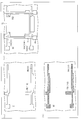
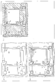
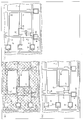
- FIG. 6 is a plan view showing a manufacturing process of the active matrix substrate according to the first embodiment.
- FIG. 6 is a plan view showing a manufacturing process of the active matrix substrate according to the first embodiment.
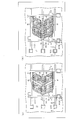
- This figure is a diagram showing a continuation of the manufacturing process shown in FIG.
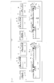
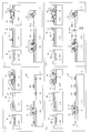
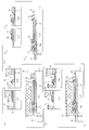
- FIG. 4 is a cross-sectional view showing a manufacturing process of the active matrix substrate shown in FIG. 3. (A) to (c) in this figure correspond to (a) to (c) in FIG. 3, respectively.
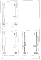
- FIG. 5 is a cross-sectional view showing a manufacturing process of the active matrix substrate shown in FIG. 4.
- FIG. 10 is a plan view showing a manufacturing process of an active matrix substrate according to a modification of the first embodiment.
- FIG. 8 is a cross-sectional view showing a manufacturing process of the active matrix substrate shown in FIG. 7.
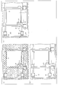
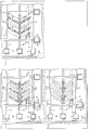
- FIG. 10 is a plan view showing a manufacturing process of the active matrix substrate according to the second embodiment.
- FIG. 10 is a plan view showing a manufacturing process of the active matrix substrate according to the second embodiment. This figure is a diagram showing a continuation of the manufacturing process shown in FIG. FIG.
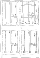
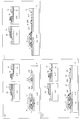
- FIG. 10 is a cross-sectional view showing a manufacturing process of the active matrix substrate shown in FIG. 9.
- (A) to (c) in this figure correspond to (a) to (c) in FIG. 9, respectively.
- FIG. 11 is a cross-sectional view showing a manufacturing process of the active matrix substrate shown in FIG. 10.
- (A) to (c) in this figure correspond to (a) to (c) in FIG. 10, respectively.
- 12 is a plan view showing a manufacturing process of an active matrix substrate according to a modification of the second embodiment.
- FIG. FIG. 14 is a cross-sectional view showing a manufacturing process of the active matrix substrate shown in FIG. 13.
- (A) to (d) in this figure correspond to (a) to (d) in FIG. 13, respectively.
- FIG. 10 is a plan view showing a manufacturing process of the active matrix substrate according to the third embodiment.
- FIG. 10 is a plan view showing a manufacturing process of the active matrix substrate according to the third embodiment.
- This figure is a diagram showing a continuation of the manufacturing process shown in FIG.
- FIG. 16 is a cross-sectional view showing a manufacturing process of the active matrix substrate shown in FIG. 15.
- (A) to (c) in this figure correspond to (a) to (c) in FIG. 15, respectively.
- FIG. 17 is a cross-sectional view showing a manufacturing process of the active matrix substrate shown in FIG. 16.
- (A) to (c) in this figure correspond to (a) to (c) in FIG. 16, respectively.
- FIG. 25 is a plan view showing a manufacturing process of an active matrix substrate according to a modification of the third embodiment.
- FIG. 20 is a cross-sectional view showing a manufacturing process of the active matrix substrate shown in FIG. 19. (A) to (c) in this figure correspond to (a) to (c) in FIG. 19, respectively.
- FIG. 10 is a plan view showing a manufacturing process of an active matrix substrate according to a fourth embodiment.
- FIG. 10 is a plan view showing a manufacturing process of an active matrix substrate according to a fourth embodiment.
- FIG. 21 is a diagram showing a continuation of the manufacturing process shown in FIG.
- FIG. 22 is a cross-sectional view showing a manufacturing step of the active matrix substrate shown in FIG. 21.
- FIG. 23 is a cross-sectional view showing a manufacturing step of the active matrix substrate shown in FIG. 22.
- (A) to (c) in this figure correspond to (a) to (c) in FIG. 22, respectively.
- FIG. 29 is a plan view showing a manufacturing process of an active matrix substrate according to a modification of the fourth embodiment.
- FIG. 26 is a cross-sectional view showing a manufacturing process of the active matrix substrate shown in FIG. 25.
- (A) to (c) in this figure correspond to (a) to (c) in FIG. 26, respectively.
- FIG. 10 is a plan view showing a manufacturing process for an active matrix substrate according to a fifth embodiment.
- FIG. 10 is a plan view showing a manufacturing process for an active matrix substrate according to a fifth embodiment.
- FIG. 10 is a plan view showing a manufacturing process for an active matrix substrate according to a fifth embodiment.
- FIG. 28 is a cross-sectional view showing a manufacturing process of the active matrix substrate shown in FIG. 27.
- (A) to (d) in this figure correspond to (a) to (d) in FIG. 27, respectively.
- FIG. 29 is a cross-sectional view showing a manufacturing process of the active matrix substrate shown in FIG. 28.
- (A) to (c) in this figure correspond to (a) to (c) in FIG. 28, respectively.
- FIG. 29 is a plan view showing a manufacturing process of an active matrix substrate according to a modification of the fifth embodiment.
- FIG. 32 is a cross-sectional view showing a manufacturing step of the active matrix substrate shown in FIG. 31.
- (A) to (c) in this figure correspond to (a) to (c) in FIG. 31, respectively.
- It is a perspective view which shows the mounting state of the conventional liquid crystal panel.
- It is an equivalent circuit diagram of a conventional liquid crystal panel.
- It is sectional drawing of the conventional liquid crystal panel.
- It is a top view which shows the manufacturing process of the conventional active matrix substrate.
- FIG. 36 shows a continuation of the manufacturing process shown in FIG.
- FIG. 37 is a cross-sectional view showing a manufacturing step of the active matrix substrate shown in FIG. 36.
- FIG. 38 is a cross-sectional view showing a manufacturing step of the active matrix substrate shown in FIG. 37.
- (A) and (b) in this figure correspond to (a) and (b) in FIG. 37, respectively.
- a coating type insulating resin is used as means for insulating the side surface of the exposed scanning signal line.
- the photosensitive resin pattern used for forming the scanning signal line is plasma-treated with a fluorine-based gas to improve water repellency.
- an insulating layer made of an insulating resin can be selectively formed so as to fill the space between the scanning signal lines.
- Patent Document 3 in the opening forming process for connecting the pixel electrode to the drain electrode, an unnecessary thin film layer such as a gate insulating layer in the pixel electrode forming region is removed. It is also possible to employ a technique for rationalizing the pixel electrode forming process by exposing the insulating layer and forming the pixel electrode on the insulating layer including the exposed drain electrode by lift-off.
- FIGS. 3 and 4 show plan views of the active matrix substrate 71 (semiconductor device for display device) according to the first embodiment of the present invention
- FIGS. 5 and 6 show A in FIG.
- Each of the plan views shown in FIGS. 3A to 3C corresponds to each of the cross-sectional views shown in FIGS. 5A to 5C, and FIG.
- Each plan view shown in (a) to (b) of FIG. 4 corresponds to each cross-sectional view shown in (a) to (b) of FIG.
- FIG. 2 shows a plan view and a sectional view (of each manufacturing process) of the active matrix substrate.
- FIGS. 7 and 8 show a plan view and a sectional view (of each manufacturing process) of an active matrix substrate as a modification of the first embodiment
- FIGS. 13 and 14 show the second embodiment.
- FIG. 19 and FIG. 20 show a plan view of an active matrix substrate as a modification and a sectional view (of each manufacturing process) of the active matrix substrate as a modification.
- FIGS. 33 to 39 show a plan view and a sectional view (of each manufacturing process) of an active matrix substrate as a modification of the fourth embodiment, and FIG. 31 and FIG. The top view and sectional drawing (each manufacturing process) of the active matrix substrate as a modification of Embodiment 5 are shown.
- the same parts as those in the conventional example shown in FIGS. 33 to 39 are denoted by the same reference numerals, and detailed description thereof is omitted.
- an active matrix substrate having a data signal line composed of a laminate of a transparent conductive layer and a second metal layer (a metal layer for source / drain wiring) is implemented in order to streamline the manufacturing process of the pixel electrode.
- a data signal line composed of a laminate of a transparent conductive layer and a second metal layer (a metal layer for source / drain wiring)
- Embodiment Modes 1 and 2 an active matrix substrate in which a pixel electrode is formed by lift-off when an opening is formed in a passivation insulating layer will be described as Embodiment Modes 3 to 5.
- FIG. 1 is a plan view showing the overall configuration of the liquid crystal display device 100
- FIG. 2 is an equivalent circuit diagram showing the electrical configuration of the pixels of the liquid crystal display device 100.
- the liquid crystal display device 100 includes an active matrix type liquid crystal panel 70, a data signal line driving circuit 45s, a scanning signal line driving circuit 45g, a storage capacitor line driving circuit 45c, and a control circuit 45.
- the liquid crystal panel 70 is configured by sandwiching liquid crystal between an active matrix substrate 71 and a counter substrate (color filter substrate) 9 described later, and has a large number of pixels P arranged in a matrix.
- the liquid crystal panel 70 includes a data signal line (source wiring) 11, a scanning signal line (gate wiring) 12, and a channel etch type insulated gate transistor (hereinafter referred to as “transistor”) 10 on an active matrix substrate 71.
- the pixel electrode 22 and the storage capacitor line 16 are provided, and the common electrode 14 is provided on the color filter substrate.
- the transistor 10 is illustrated only in FIG. 2 and omitted in FIG.
- One data signal line 12 is formed in each column so as to be parallel to each other in the column direction (vertical direction), and the scanning signal line 11 is arranged in each row so as to be parallel to each other in the row direction (horizontal direction).
- the transistor 10 and the pixel electrode 22 are formed corresponding to the intersections of the data signal line 12 and the scanning signal line 11, respectively.
- the source electrode s of the transistor 10 is the data signal line 12, and the gate electrode g is the scanning signal.
- the drain electrode d is connected to the pixel electrode 22 on the line 11. Further, the pixel electrode 22 forms a liquid crystal capacitor 13 between the counter electrode 14 via a liquid crystal.
- the gate of the transistor 10 is turned on by the gate signal (scanning signal) supplied to the scanning signal line 11, the source signal (data signal) from the data signal line 12 is written to the pixel electrode 22, and the pixel electrode 22 is It is possible to realize gradation display according to the source signal by setting the potential according to the source signal and applying a voltage according to the source signal to the liquid crystal interposed between the counter electrode 14. it can.
- the storage capacitor lines 16 are formed one by one in each row so as to be parallel to each other in the row direction (lateral direction), and are arranged to make a pair with the scanning signal line 11.
- Each storage capacitor line 16 is capacitively coupled to the pixel electrode 22 arranged in each row, and forms a storage capacitor (auxiliary capacitor) 15 between each pixel electrode 22.
- the liquid crystal panel 70 having the above configuration is driven by a data signal line driving circuit 45s, a scanning signal line driving circuit 45g, a storage capacitor line driving circuit 45c, and a control circuit 45 for controlling them.
- the horizontal scanning period of each row is sequentially assigned, and each row is sequentially scanned.
- the scanning signal line driving circuit 45g sequentially outputs a gate signal for turning on the transistor 10 to the scanning signal line 11 of the row in synchronization with the horizontal scanning period of each row.
- the data signal line driving circuit 45 s outputs a source signal to each data signal line 12.
- This source signal is a signal obtained by assigning a video signal supplied from the outside of the liquid crystal display device 1 to the data signal line driving circuit 45s via the control circuit 45 to each column in the data signal line driving circuit 45s and performing boosting or the like. It is.
- the storage capacitor line drive circuit 45 c outputs a CS signal to each storage capacitor line 16.
- This CS signal is, for example, a signal whose potential is switched between two values (rises or falls), and is synchronized with the end of the horizontal scanning period (1H) of each row, that is, the transistor 10 of each row is turned off. At the time of switching to, the potential of the storage capacitor line 16 of the row is switched from one value to the other value.
- the control circuit 45 outputs a gate signal, a source signal, and a CS signal from each of these circuits by controlling the scanning signal line driving circuit 45g, the data signal line driving circuit 45s, and the storage capacitor line driving circuit 45c. It is something to be made.
- a first metal layer (for scanning signal lines) having a film thickness of about 0.1 to 0.3 ⁇ m is formed on one main surface of the glass substrate 2 using a vacuum film forming apparatus such as SPT.
- a metal layer may be, for example, a single layer metal such as Ti, Ta, Cr, and Mo.
- Al or a heat-resistant Al alloy is used, and the battery effect in an alkaline liquid with the transparent conductive layer is obtained.
- a laminated structure such as Ti / Al / Ti, Mo / Al / Mo, or Al (Nd) / Mo is desirable.
- Al (Nd) means a highly heat-resistant Al alloy containing several percent or less of Nd, and an Al alloy containing Ni, Ta, Hf or the like instead of Nd has no problem. It is also possible to use Cu or a Cu alloy instead of Al for low resistance.
- a first SiNx layer 30 that becomes a gate insulating layer, a first amorphous silicon layer that hardly contains impurities and becomes a channel of an insulated gate transistor Three types of thin film layers, ie, a semiconductor layer 31 and a second amorphous silicon layer (semiconductor layer) 33 containing impurities and serving as the source and drain of an insulated gate transistor, are, for example, 0.3-0.2-
- the film is sequentially deposited with each film thickness of about 0.05 ⁇ m, and a thin film layer 34 of, for example, Mo or Ti is deposited as a heat-resistant metal layer with a film thickness of about 0.1 ⁇ m using a vacuum film forming apparatus such as SPT. .
- a photosensitive resin pattern PR (first photosensitive resin pattern) corresponding to the scanning signal line 11 is obtained by photolithography.
- the first metal layer is selectively removed in addition to the refractory metal layer 34, the second amorphous silicon layer 33, the first amorphous silicon layer 31, and the gate insulating layer 30. Then, the glass substrate 2 is exposed.
- the refractory metal layer 34 is Mo (Ti)
- Mo (chlorine) gas the fluorine-based (chlorine) gas
- the second amorphous silicon layer 33 the first amorphous layer is removed.
- the porous silicon layer 31 and the gate insulating layer 30 are removed by dry etching using a fluorine-based gas.
- the first metal layer is Mo, Ti, or Ta
- Mo the first metal layer
- Cr it is removed using a dedicated etching solution.
- the first metal layer is a laminated layer of Mo / Al / Mo or Al (Nd) / Mo, it is removed by wet etching using a mixed acid obtained by adding several percent nitric acid to phosphoric acid.
- a plasma treatment of a freon gas such as CF 4 is performed on the entire surface of the glass substrate 2.
- the photosensitive resin pattern PR is an organic resin, and thus the surface is easily fluorinated to become the photosensitive resin pattern PR1 ((b in FIG. 5). )reference). Fluorination is sufficient if the surface depth is 100 mm or more.
- an inorganic transparent resin transparent inorganic insulation
- silicon oxide fine powder is dissolved in a solvent together with a binder as a coating-type transparent insulating resin.
- Resin or transparent resin such as acrylic resin having high heat resistance and high transparency is applied to the glass substrate 2. Since the fluorinated photosensitive resin pattern PR1 has water repellency, the transparent insulating resin is repelled on the photosensitive resin pattern PR1 and applied in a self-aligning manner to the region except on the photosensitive resin pattern PR1. If a photosensitive resin having no water repellency is used, the transparent insulating resin cannot be selectively filled. Here, the transparent insulating resin is applied with substantially the same film thickness as the multilayer film pattern.
- the solvent contained in the transparent insulating resin 60 is heated and evaporated so as not to hinder the removal by the resist stripping solution, and then ashing means such as oxygen plasma
- ashing means such as oxygen plasma
- the polymer on the surface fluorinated by the step is removed, and the photosensitive resin pattern PR1 is removed using a resist stripping solution.
- the transparent insulating resin 60 is an acrylic resin
- the film thickness is reduced by 100 mm or more by the oxygen plasma treatment.
- the film thickness of the transparent insulating resin 60 usually exceeds 0.5 ⁇ m, there is almost no influence.
- the heat treatment (usually about 250 ° C.) is performed as much as possible within a range in which the film quality of the amorphous silicon layers 31A and 33A is not deteriorated, thereby improving the film quality of the transparent insulating layer 60 and enhancing the chemical resistance.
- a source / drain wiring forming step is performed.
- a transparent conductive layer 91 having a thickness of about 0.1 ⁇ m and a second metal layer (a metal layer for source / drain wiring) 35 are deposited on the entire surface of the glass substrate 2 using a vacuum film forming apparatus such as SPT.
- the second metal layer 35, the transparent conductive layer 91, the refractory metal layer 34A, and the second amorphous silicon layer 33A are formed by a fine processing technique using the photosensitive resin pattern (second photosensitive resin pattern).
- the first amorphous silicon layer 31A is etched to leave about 0.05 to 0.1 ⁇ m.
- the source is formed by stacking the transparent conductive layer 91A and the second metal layer 35A formed so as to partially overlap the gate electrode 11.
- a data signal line 12 also serving as a wiring, a pseudo electrode terminal P6 formed of a part of the data signal line 12, a transparent conductive layer 91B formed so as to partially overlap the gate electrode 11, and a second metal layer 35B
- the drain electrode 21 of the insulated gate transistor that also serves as the pseudo pixel electrode P22 is selectively formed.
- Al is generally used as the second metal layer 35.
- the transparent conductive layer disappears due to the battery reaction in the alkaline liquid developer or resist stripping solution, the laminated structure of Al and the transparent conductive layer is used as a buffer metal layer between Al and the transparent conductive layer. It is necessary to interpose Mo.
- a heat-resistant metal such as Ti, Cr, Mo as the second metal layer to simplify the configuration of the data signal line.
- the second metal has a stacked structure of Mo having a thickness of about 0.1 ⁇ m as the buffer metal layer 36 having a thickness of about 0.1 ⁇ m and an Al thin film layer 35 as a low resistance metal layer having a thickness of about 0.3 ⁇ m. Selected as a layer.
- the second metal layer can be formed into a single layer by adding, for example, Ni, La or the like.
- the transparent conductive layer 91 needs to have a resistance not to be etched with respect to the mixed acid so that the transparent conductive layer 91 is not lost in the pixel electrode exposure step described later. Note that the above-described problem can be avoided if the transparent conductive layer has a film quality that is changed by a heat treatment at about 250 ° C. in the deposition process of the passivation insulating layer subsequent to the source / drain wiring formation process.
- the transparent conductive layer 91 having such properties examples include ITZO (Indium-Tin-Zinc-Oxide) having a low crystallization temperature of 200 ° C.
- ITZO Indium-Tin-Zinc-Oxide
- an ITZO film with a sputtering target ITZ composition ratio of 85: 10: 5 undergoes a heat treatment at 250 ° C., which is the deposition temperature of SiNx, which is a passivation insulating layer, and the film quality changes from amorphous to microcrystalline. To do. Therefore, the ITZO film is a very unique material that is resistant to the mixed acid in the pixel electrode exposure process.
- a second SiNx layer having a thickness of about 0.3 ⁇ m is deposited on the entire surface of the glass substrate 2 as a transparent insulating layer using a PCVD apparatus. And thereafter, as shown in FIGS. 4A and 6A, the photosensitive resin pattern (third photosensitive resin pattern) is used to form the electrode terminals 5 on the pseudo pixel electrode P22 and the scanning signal line.
- the openings 38 (first opening), 63 (second opening), and 64 (third opening) are formed on the pseudo electrode terminal P6, respectively.
- the passivation insulating layer 37 in each opening is first removed to expose the pseudo pixel electrode P22, the first amorphous silicon layer 31A, and the pseudo electrode terminal P6. Subsequently, the second metal layer 35 (and the buffer metal layer 36) in the openings 38 and 64 is selectively removed to expose most of the transparent conductive pixel electrode 22 and the transparent conductive electrode terminal 6A.
- the ITZO film with an ITZ composition ratio of 85: 10: 5 is given crystallinity by the heat treatment applied during the formation of the passivation insulating layer, so the second metal layer 35 (and the buffer metal layer 36) is removed using a mixed acid. Even in this case, the pixel electrode 22 and the electrode terminal 6A are not reduced or lost.
- the first amorphous silicon layer 31A and the gate insulating layer 30A in the opening 63 are removed to expose most of the electrode terminals 5 of the scanning signal lines.
- the removal of the first amorphous silicon layer 31A and the gate insulating layer 30A is performed by dry etching of a fluorine-based gas. At this time, however, the pixel electrode 22 and the electrode terminal 6A made of an ITZO film have durability and the film is reduced. Or disappear.
- the active matrix substrate 71 thus obtained and the color filter substrate 9 (counter substrate) are bonded to form a liquid crystal panel, and the manufacturing process of the first embodiment is completed.
- a part 72 of the pseudo pixel electrode P22 and the scanning signal line 11 in the previous stage are composed of the refractory metal layer 34A and the first.
- a pattern design in which the storage capacitor 15 is constituted by a region 51 (inclined to the right) that is planarly overlapped with the second amorphous silicon layer 33A, the first amorphous silicon layer 31A, and the gate insulating layer 30A. Is illustrated.
- a half-process is performed by the scanning signal line and semiconductor layer forming process, the source / drain wiring and pseudo pixel electrode forming process, and the opening forming process in the passivation insulating layer.
- the active matrix substrate 71 is obtained using three photomasks without using the tone exposure technique.
- the final photoetching process is an opening forming process in the passivation insulating layer, there is no way to connect the electrode terminal 5 of the scanning signal line and the electrode terminal 6A of the data signal line with an appropriate conductive material, Static electricity countermeasures cannot be applied. Therefore, careful handling is required in the panel assembly process / inspection process after the active matrix substrate is completed.
- a black pigment dispersed photosensitive resin 90 is used instead of a normal photosensitive resin.
- the photosensitive black pigment resin 90 is not removed and the active matrix substrate 71 is formed. It may be completed. Thereby, the photosensitive black pigment resin 90 can also function as a BM (black matrix), and the manufacturing cost of the liquid crystal panel can be further reduced.
- the streamlined active matrix substrate described in the first embodiment has a TN liquid crystal mode, but the present invention is also effective for a vertical alignment liquid crystal having a wide viewing angle by changing the shape of the pixel electrode. is there. This will be described as a part of the first embodiment.
- An alignment control means that can be formed on the active matrix substrate 71 constituting the vertical alignment type liquid crystal panel is to provide a slit in the pixel electrode or a protrusion on the pixel electrode, and this basic configuration is the active matrix of the first embodiment.
- the transparent conductive pixel electrodes 22-1 to 22-4 formed in a plurality of strips form the storage electrode 72.
- the pixel electrode 22-1 is formed with the pixel electrode 22-3, and the pixel electrode 22-2 is formed substantially orthogonal to the pixel electrode 22-4 for the alignment division.
- a gap 42 between the pixel electrode 22-1 and the pixel electrode 22-2 and between the pixel electrode 22-3 and the pixel electrode 22-4 functions as a slit (cut).
- 72 is a storage electrode formed at the same time as the source / drain wirings 12 and 21, and constitutes the storage capacitor 15 through an insulating layer including the storage capacitor line 16 and the gate insulating layer 30B.
- a projection 40 made of a photosensitive resin having a bowl-shaped cross section is formed on the counter electrode 14. As a result, the viewing angle is increased by aligning and dividing the direction in which the liquid crystal molecules are inclined by applying a voltage to the liquid crystal cell in four directions.
- the counter electrode 14 may be partially removed instead of the protrusion 40 to form a slit (cut).
- the slit 42 formed in the gap between the pixel electrode 22-1 and the pixel electrode 22-2 and between the pixel electrode 22-3 and the pixel electrode 22-4 is compared with the inside of the pixel electrodes 22-1 to 22-4. Since a horizontal component is generated in the lines of electric force, the alignment direction of the vertically aligned liquid crystal molecules is determined by the horizontal component. However, if no voltage is applied to the liquid crystal, electric lines of force are not generated, so the alignment control force is weaker than that of the protrusion.
- the two transparent conductive pixel electrodes 22A and 22B are substantially orthogonal to the drain electrode 21 via the storage electrode 72.
- a stacked pattern is formed which is formed by stacking the passivation insulating layer 37P and the second metal layer (the buffer metal layer 36P and the low-resistance metal layer 35P) on substantially the center of the pixel electrode 22A and the pixel electrode 22B. This laminated pattern functions as the protrusion 41.
- 72 is a storage electrode formed at the same time as the source / drain wirings 12 and 21, and constitutes the storage capacitor 15 through an insulating layer including the storage capacitor line 16 and the gate insulating layer 30B.
- the cross-sectional shape of the transparent conductive counter electrode 14 formed on the color filter substrate 9 facing the active matrix substrate 71 is in a region corresponding to the substantially central portion of the two pixel electrodes 22A and 22B.
- a protrusion 40 made of a bowl-shaped photosensitive resin is formed.
- the pixel electrodes 22A-1 and 22B-1 divided by the protrusions 41 on the pixel electrode and the pixel electrodes 22A-2 and 22B-2 are substantially orthogonal to each other for the alignment division. As a result, the viewing angle is increased by dividing the direction in which the liquid crystal molecules are inclined by applying a voltage to the liquid crystal cell in four directions.
- the vertical alignment type liquid crystal molecules are aligned vertically along the side surface.
- the thickness of the passivation insulating layer 37P is usually 0.3 ⁇ m, and a strong regulation force cannot be expected, but the response speed of the liquid crystal is slightly improved and increased as compared with a vertical alignment type liquid crystal panel provided with a slit in the pixel electrode.
- the above-described active matrix substrate according to the first embodiment can not only incorporate a countermeasure against static electricity, but also has a first amorphous silicon layer 31A whose thickness is reduced on the scanning signal line 11 via the gate insulating layer 30A. Therefore, the crosstalk between the data signal lines cannot be completely suppressed, and there is a limit in improving the display image quality.
- a halftone exposure technique introduced to solve these problems will be described as a second embodiment shown below.
- the configuration of the liquid crystal display device 100 according to the second embodiment is the same as that of the liquid crystal display device 100 according to the first embodiment described with reference to FIG. 1 and FIG.
- a first metal layer (a metal layer for a scanning signal line) having a film thickness of about 0.1 to 0.3 ⁇ m is formed on one main surface of the glass substrate 2. Adhere.
- the three types of thin film layers, ie, the second amorphous silicon layer 33 to be formed are sequentially deposited with respective film thicknesses of, for example, about 0.3-0.2-0.05 ⁇ m, and vacuum film formation such as SPT is performed.
- a thin film layer 34 of, for example, Mo or Ti is deposited as a heat-resistant metal layer having a thickness of about 0.1 ⁇ m.
- the film 83 of the pattern 83A corresponding to the scanning signal line 11 has a thickness of, for example, 2 ⁇ m using the halftone exposure technique, and the scanning signal line connection region 5 (outside the image display unit).
- Photosensitive resin patterns 83A and 83B (first photosensitive resin pattern) in which the film thickness of the pattern 83B corresponding to other wiring lines provided outside the image display portion in the scanning signal line is 1 ⁇ m, for example. ) Is formed on the refractory metal layer 34. Thereafter, as shown in FIGS.
- the heat-resistant metal layer 34, the second amorphous silicon layer 33, the first heat-resistant metal layer 34, and the first amorphous silicon layer 33 are formed using the photosensitive resin patterns 83A and 83B as a photomask.
- the glass substrate 2 is exposed by selectively removing the first metal layer in addition to the amorphous silicon layer 31 and the gate insulating layer 30.
- a plasma treatment of a freon gas such as CF 4 is performed on the entire surface of the glass substrate 2.
- the photosensitive resin patterns 83A and 83B are organic resin, so that the surface is easily fluorinated to become photosensitive resin patterns 83A1 and 83B1. Fluorination is sufficient if the surface depth is 100 mm or more.
- an inorganic transparent resin obtained by dissolving silicon oxide fine powder in a solvent together with a binder as a coating type transparent insulating resin is applied to the glass substrate 2. Since the fluorinated photosensitive resin patterns 83A1 and 83B1 have water repellency, the transparent insulating resin is repelled on the photosensitive resin patterns 83A1 and 83B1, and is shown in FIGS. 9B and 11B. As described above, the coating is applied in a self-aligned manner to the regions except on the photosensitive resin patterns 83A1 and 83B1. Here, the transparent insulating resin is applied with substantially the same film thickness as the multilayer film pattern.
- the solvent contained in the transparent insulating resin 60 is heated and evaporated so as not to hinder the removal by the resist stripping solution, and further, ashing means such as oxygen plasma is used.
- ashing means such as oxygen plasma is used.
- the film thickness of the photosensitive resin patterns 83A1 and 83B1 is reduced by 1 ⁇ m or more.
- the photosensitive resin pattern 83B1 disappears and an opening 63A is formed.
- the heat-resistant metal layer 34A is exposed in the opening 63A, and the photosensitive resin pattern 83C is selectively formed only on the scanning signal line formation region. can do.
- the transparent insulating resin 60 is an acrylic resin
- the film is reduced by the oxygen plasma treatment and disappears. Therefore, unlike the first embodiment, the acrylic resin cannot be used for the coating type transparent insulating resin. .
- the heat-resistant metal layer 34A, the second amorphous silicon layer 33A, the first amorphous silicon layer 33A in the opening 63A are formed using the photosensitive resin pattern 83C as a mask.
- the amorphous silicon layer 31A and the gate insulating layer 30A are selectively removed to expose the scanning signal line connection region 5 (cross-sectional view taken along line BB ′ in FIG. 11C).
- the photosensitive resin pattern 83C is removed using a resist stripping solution. Further, heat treatment (usually about 250 ° C.) is performed as much as possible within the range where the film quality of the amorphous silicon layers 31A and 33A is not deteriorated, thereby improving the film quality of the transparent insulating layer 60.
- a source / drain wiring forming step is performed.
- a transparent conductive layer 91 having a thickness of about 0.1 ⁇ m and a second metal layer (a metal layer for source / drain wiring) 35 are deposited on the entire surface of the glass substrate 2 using a vacuum film forming apparatus such as SPT.
- the second metal layer 35, the transparent conductive layer 91, the refractory metal layer 34A, and the second amorphous silicon layer 33A are formed by a fine processing technique using the photosensitive resin pattern (second photosensitive resin pattern).
- the first amorphous silicon layer 31A is etched to leave about 0.05 to 0.1 ⁇ m.
- the source is formed by stacking the transparent conductive layer 91A and the second metal layer 35A formed so as to partially overlap the gate electrode 11.
- the drain of the insulated gate transistor which also comprises the data signal line 12 which also serves as wiring, and a laminated layer of the transparent conductive layer 91B and the second metal layer 35B which are also formed so as to partially overlap the gate electrode 11, and which also serves as the pseudo pixel electrode P22.
- An electrode 21 is selectively formed.
- the scanning comprising the connection region 5 of the scanning signal line exposed in the region outside the image display portion is formed by laminating the transparent conductive layer 91C and the second metal layer 35C.
- the laminated structure of the buffer metal layer 36 and the Al thin film layer 35 is referred to as a second metal layer.
- a second SiNx layer having a thickness of about 0.3 ⁇ m is deposited on the entire surface of the glass substrate 2 as a transparent insulating layer using a PCVD apparatus.
- the scanning signal line 11, the pseudo pixel electrode P22, the scanning signal line pseudo electrode terminal 5, and the data signal line pseudo electrode terminal P6 are formed using a photosensitive resin pattern (third photosensitive resin pattern).
- the passivation insulating layer in the openings 75, 38, 63 and 64 is removed by dry etching with a fluorine-based gas.
- the first amorphous silicon layer 31A in the opening 75 is removed by either switching the gas or overetching, and the gate insulating layer is formed in the openings 75, 38, 63, and 64, respectively.
- 30A, the transparent insulating layer 60, the pseudo pixel electrode 22, the pseudo electrode terminal 5A, and the pseudo electrode terminal 6A are exposed.
- the second metal layer 35 in the openings 38, 63 and 64 is removed by wet etching using a mixed acid, and the pixel electrode 22 made of a transparent conductive layer, the electrode terminal 5A of the scanning signal line, and the data signal are all used. Most of the electrode terminal 6A of the wire is exposed.
- the active matrix substrate 71 and the color filter substrate 9 thus obtained are bonded to form a liquid crystal panel, and the manufacturing process of the second embodiment is completed.
- the configuration of the storage capacitor 15 is the same as that of the first embodiment.
- the connection region 5 of the scanning signal line is exposed before the source / drain wirings 12 and 21 are formed, the space between the electrode terminal 5A of the scanning signal line and the electrode terminal 6A of the data signal line is transparent. It is possible to take measures against static electricity connected by a short-circuit wire 44 made of a conductive layer.
- the opening 75 is formed on the scanning signal line 11 and the first amorphous silicon layer 31A in the opening is removed. Since the array configuration is adopted, the formation of parasitic transistors can be prevented and the possibility of crosstalk is also eliminated.
- the step of forming the scanning signal line and the semiconductor layer using the halftone exposure technique and the formation of the contact to the scanning signal line, the formation of the source / drain wiring and the pseudo pixel electrode The active matrix substrate 71 is obtained using three photomasks by the process and the process of forming an opening in the passivation insulating layer.
- the final photolithography process is an opening forming process in the passivation insulating layer
- a black pigment dispersion type photosensitive film is used instead of a normal photosensitive resin in forming the opening in the passivation insulating layer.
- the gate insulating layer 30A, the transparent insulating layer 60, and the pixel electrode are formed in the openings 75, 38, 63, and 64, respectively, using the conductive resin 90. 22.
- the photosensitive black pigment resin 90 is made BM by completing the active black substrate 71 without removing the photosensitive black pigment resin 90. It is also possible to function as in the first embodiment.
- the streamlined active matrix substrate described in the second embodiment has a TN liquid crystal mode, but the present invention can be applied to an IPS liquid crystal and a vertical alignment liquid crystal having a wide viewing angle by changing the shape of the pixel electrode.
- the invention is effective. This will be described below as a part of the second embodiment.
- a basic configuration having a counter electrode formed on the active matrix substrate 71 and a pixel electrode formed at a predetermined distance from the counter electrode as a pair of electrodes is applied to the active matrix substrate 71 of the second embodiment. Then, as shown in FIGS. 13A and 14A, a plurality of strip-like counter electrodes 16A branched into the pixel from the storage capacitor line 16 formed simultaneously with the scanning signal line 11, and the drain A plurality of strip-shaped pixel electrodes 21 ⁇ / b> A connected to the electrode 21 are formed at a predetermined distance.
- the counter electrode 16A and the pixel electrode 21A are inclined by several degrees with respect to the data signal line 12 in the upper half and the lower half of the pixel.
- the counter electrode 16A and the pixel electrode 21A do not have to be transparent conductive.
- the counter electrode 14 is not necessary on the color filter substrate 9.
- Reference numeral 72 denotes a storage electrode formed at the same time as the source / drain wirings 12 and 21, and constitutes the storage capacitor 15 with the storage capacitor line 16 via an insulating layer including a gate insulating layer 30B (not shown). To do.
- the display image is required unless the pattern alignment accuracy of these electrodes is high. There is a high possibility that brightness spots will occur. Therefore, it is also possible to obtain an IPS liquid crystal panel having a different configuration by changing the arrangement position of the counter electrode.
- the counter electrode 21 ⁇ / b> B made of the second metal layer is formed on a part of the storage capacitor line 16 without being assigned a number. It is formed on the transparent insulating layer 60 at the same time as the source / drain wirings 12 and 21 including the opened openings.
- both the counter electrode 21B and the pixel electrode 21A are formed on the transparent insulating layer 60, the probability that these electrodes are short-circuited increases.
- luminance spots occur in the display image due to the effect of pattern alignment accuracy at these inter-electrode distances.
- there is no insulating layer on the counter electrode 21B and the pixel electrode 21A, which are display electrodes there is an advantage that display image burn-in does not occur as compared with the conventional IPS liquid crystal panel.
- Alignment control means that can be formed on the active matrix substrate 71 constituting the vertical alignment type liquid crystal panel includes providing slits in the pixel electrode or protrusions on the pixel electrode.
- the transparent conductive pixel electrode 22 formed in a plurality of strips. -1 to 22-4 are connected to the drain electrode 21 via the storage electrode 72, and the pixel electrode 22-1 is connected to the pixel electrode 22-3 and the pixel electrode 22-2 is connected to the pixel electrode 22-4 for division of orientation. And substantially orthogonal to each other.
- the gap 42 between the pixel electrode 22-1 and the pixel electrode 22-2 and between the pixel electrode 22-3 and the pixel electrode 22-4 functions as a slit (cut).
- the two transparent conductive pixel electrodes 22A and 22B are substantially orthogonal to the drain electrode 21 via the storage electrode 72.
- a stacked pattern is formed that is formed by stacking the passivation insulating layer 37P and the second metal layer (the buffer metal layer 36P and the low-resistance metal layer 35P) on substantially the center of the pixel electrode 22A and the pixel electrode 22B. This laminated pattern functions as the protrusion 41.
- Embodiment 3 Subsequently, Embodiment 3 will be described below.
- the configuration of the liquid crystal display device 100 according to the third embodiment is the same as that of the liquid crystal display device 100 according to the first embodiment described with reference to FIGS. 1 and 2, the description thereof is omitted.
- First step scanning signal line and semiconductor layer forming step
- a first metal having a film thickness of about 0.1 to 0.3 ⁇ m is formed on one main surface of the glass substrate 2 using a vacuum film forming apparatus such as SPT.
- a layer (a metal layer for the scanning signal line) is deposited.
- a first SiNx layer 30 which becomes a gate insulating layer
- a first amorphous silicon layer 31 which hardly contains impurities and becomes a channel of an insulated gate transistor
- the photosensitive resin pattern PR (first photosensitive resin pattern) corresponding to the scanning signal line 11 is exposed by the photolithography technique.
- the glass substrate 2 is removed by selectively removing the first metal layer in addition to the second amorphous silicon layer 33, the first amorphous silicon layer 31 and the gate insulating layer 30 using the conductive resin pattern PR as a mask. Exposed.
- the second amorphous silicon layer 33, the first amorphous silicon layer 31, and the gate insulating layer 30 are removed by dry etching using a fluorine-based gas.
- the first metal layer is Mo, Ti, or Ta, it is subsequently removed by dry etching.
- the first metal layer is Cr, it is removed using a dedicated etching solution.
- the first metal layer is a laminated layer of Mo / Al / Mo or Al (Nd) / Mo, it is removed by wet etching using a mixed acid obtained by adding several percent nitric acid to phosphoric acid.
- the entire surface of the glass substrate 2 is obtained. Then, a plasma treatment of a freon gas such as CF 4 is performed. Thereby, the surface of the photosensitive resin pattern PR is fluorinated to form a photosensitive resin pattern PR1.
- an inorganic transparent resin transparent inorganic insulation
- silicon oxide fine powder is dissolved in a solvent together with a binder as a coating-type transparent insulating resin.
- Resin transparent resin
- transparent resin such as acrylic resin having high heat resistance and high transparency is applied to the glass substrate 2.
- the solvent contained in the transparent insulating resin 60 is heated and evaporated, and then the polymer on the surface fluorinated by ashing means such as oxygen plasma is removed.
- the photosensitive resin pattern PR1 is removed using a resist stripping solution. Further, the heat treatment (usually about 250 ° C.) is performed as much as possible within the range where the film quality of the amorphous silicon layers 31A and 33A is not deteriorated, thereby improving the film quality of the transparent insulating resin 60.
- a source / drain wiring forming step is performed.
- a second metal layer (a metal layer for source / drain wiring) is deposited on the entire surface of the glass substrate 2, as shown in FIGS. 15 (c) and 17 (c)
- fine processing is performed.
- the second metal layer is etched using a photosensitive resin pattern (second photosensitive resin pattern) by a technique.
- the data signal line 12 having the data signal line connection region 6 in a region outside the image display portion and partially serving as the source wiring of the insulated gate transistor so as to partially overlap the gate electrode 11A and the gate electrode 11A.
- the drain electrode 21 of the insulated gate transistor and the storage electrode 72 are selectively formed on the scanning signal line 11 so as to overlap each other. Subsequently, the second amorphous silicon layer 33A and the first amorphous silicon layer 31A are sequentially etched, and the first amorphous silicon layer 31A is etched leaving about 0.05 to 0.1 ⁇ m. .
- the step absorption electrode 5S is also formed across the boundary between the scanning signal line connection region 5 and the transparent insulating layer 60 simultaneously with the formation of the source / drain wirings 12 and 21.
- a refractory metal such as Ti, Cr, or Mo is used as in the other embodiments.
- a heat-resistant metal layer having a film thickness of about 0.1 ⁇ m a thin film layer 34 of, for example, Mo or Ti
- An Al thin film layer 35 is selected as a low resistance metal layer having a thickness of about 0.3 ⁇ m, and a thin film layer 36 of Mo, Ti, or the like is selected as a buffer metal layer having a thickness of about 0.1 ⁇ m.
- the buffer metal layer 36 is required in this way.
- the configuration of the second metal layer is Mo / Al / Mo
- mixed acid phosphoric acid containing nitric acid
- the configuration of the second metal layer is Ti / Al / Ti.
- a second SiNx layer having a thickness of about 0.3 ⁇ m is deposited as a transparent insulating layer on the entire surface of the glass substrate 2 to form a passivation insulating layer 37.
- Openings 38 (first opening), 63 (second opening), and 64 (second opening) are formed in the connection region 5 of the scanning signal line 11 including the absorption electrode 5S and the connection region 6 of the data signal line 12, respectively.
- a photosensitive resin pattern (third photosensitive resin pattern) 88 having a third opening) is formed.
- the cross-sectional shape of each opening part is reverse taper shape.
- the product name TELR-N101PM manufactured by Tokyo Ohka Kogyo Co., Ltd. may be used as the photosensitive resin in which the cross-sectional shape of the opening has an inversely tapered shape. A film thickness of 1 ⁇ m or more is sufficient.
- This product was developed for the purpose of dividing the conductive thin film layer for the electrode to be deposited into the opening in the electrode formation process after the formation of the organic EL light emitting layer in the manufacture of the organic EL display device. is there.
- This product is a chemically amplified negative photosensitive resin. The difference from a normal positive photosensitive resin is that a heat treatment (Post-Exposure-Bake) must be performed after exposure prior to development processing. There is a point.
- the passivation insulating layer 37 in the openings 38 and 64 is removed using the photosensitive resin pattern 88 as a mask, and the transparent insulating layer 60 is removed.
- a part of each of the drain electrode 21, a part of the storage electrode 72, and the connection region 6 between the transparent insulating layer 60 and the data signal line 12 are exposed.
- the passivation insulating layer 37, the first amorphous silicon layer 31A, and the gate insulating layer 30A in the opening 63 are removed, and the transparent insulating layer 60, the step absorption electrode 5S, and one of the scanning signal lines 11 are removed.
- the connection region 5 which is a part is exposed.
- the transparent conductive layer 91 is formed on the glass substrate 2 by using a vacuum film forming apparatus such as SPT without removing the photosensitive resin pattern 88.
- ITO, IZO, or a mixed crystal thereof having a film thickness of about 0.1 ⁇ m is deposited.
- the transparent conductive layer 91 has a thin film thickness as described above, and the cross-sectional shape is an inversely tapered shape, the transparent conductive layer 91 deposited on the side surface of the photosensitive resin pattern 88 is extremely Few.
- the photosensitive resin pattern 88 is removed using a resist stripping solution or a specific organic solvent, melting starts from the side of the photosensitive resin pattern 88, and the transparent conductive layer 91 on the photosensitive resin pattern 88 is easily formed. It will peel off. This is a so-called lift-off.
- the transparent insulation in the opening 38 which is a pixel electrode formation region including a part of the drain electrode 21 and a part of the storage electrode 72 is obtained.
- the pixel electrode 22 is formed in a self-aligning manner.
- the scanning signal line electrode terminal 5A is formed in a self-aligned manner in the opening 63 including a part (connection region) 5 of the scanning signal line and the step absorption electrode 5S. Furthermore, in the opening 64 including the connection region 6 of the data signal line 12, the electrode terminal 6A of the data signal line is formed in a self-aligning manner. In addition, the passivation insulating layer 37 on the glass substrate 2 is exposed, and the manufacturing process of the active matrix substrate 71 is completed.
- the photosensitive resin pattern 88 is altered if the heating temperature is too high, and it is difficult to remove the substrate in the lift-off process.
- the temperature is desirably 150 ° C. or lower.
- the active matrix substrate 71 and the color filter substrate 9 thus obtained are bonded to form a liquid crystal panel, and the manufacturing process of the third embodiment is completed.
- the storage electrode 72 and the scanning signal line 11 in the previous stage are planar through the second amorphous silicon layer 33A, the first amorphous silicon layer 31A, and the gate insulating layer 30A.
- the example (it is not illustrated here. Refer to the downward slanting slanting line part 51 shown to (a) of FIG. 4) is illustrated.
- the transparent conductive short-circuit wire 44 is obtained by forming the opening 66 in the outer peripheral portion of the active matrix substrate 71 as in the conventional example, and is short-circuited with the transparent conductive electrode terminals 5A and 6A. By forming an elongated stripe between the wires 44, the resistance is increased and the resistance against static electricity is increased.
- a half-process is performed by each of the scanning signal line and semiconductor layer forming process, the source / drain wiring forming process, and the opening to the passivation insulating layer and the pixel electrode forming process.
- An active matrix substrate is manufactured using three photomasks without using a tone exposure technique. Accordingly, there is no variation in the pattern width due to the influence of halftone exposure, so that a secondary effect that the dimension management in each patterning process may be at a normal level can be obtained.
- Embodiment 3 Modification of Embodiment 3
- the present invention can be applied to IPS liquid crystal and vertical alignment type liquid crystal having a wide viewing angle by changing the shape of the pixel electrode. This is effective and will be described as a part of the third embodiment.
- the passivation insulating layer 37 on the transparent insulating layer 60 is provided.
- a plurality of transparent conductive layers formed in the openings formed in the passivation insulating layer 37 on the transparent insulating layer 60 are used.
- the pixel electrode 16C and the counter electrode 16A, which are display electrodes are both transparent conductive layers, the leakage electric field around the display electrode is used to reflect the increase in the transmittance of the IPS liquid crystal panel. Is also easier.
- the pixel electrode 21A made of the second metal layer and the counter electrode 16A made of the transparent conductive layer are both formed on the transparent insulating layer 60, but the pixel electrode 21A is made of the passivation insulating layer 37.
- the probability that these electrodes are short-circuited is low.
- the pattern alignment accuracy of these electrodes is not high, there is a high possibility that luminance spots will appear in the display image.
- both the counter electrode 16A and the pixel electrode 16C made of a transparent conductive layer are formed on the transparent insulating layer 60, these electrodes are short-circuited.
- the probability is high, there is no possibility that brightness spots will appear in the display image due to the effect of pattern alignment accuracy at these inter-electrode distances.
- the latter since there is no insulating layer on the counter electrode 16A and the pixel electrode 16C, which are display electrodes, the latter has the advantage that the display image is less burned when compared.
- Alignment control means that can be formed on the active matrix substrate 71 constituting the vertical alignment type liquid crystal panel includes providing slits in the pixel electrode or protrusions on the pixel electrode.
- the slit and the protrusion are formed at the same time due to the peculiarity of the pixel electrode forming process.
- the transparent conductive pixel electrodes 22-1 to 22-4 formed in a plurality of strips are drained via the storage electrode 72.
- the pixel electrode 22-1 is connected to the electrode 21 and the pixel electrode 22-1 is formed substantially orthogonal to the pixel electrode 22-4 and the pixel electrode 22-2 is formed substantially orthogonal to the pixel electrode 22-4 for alignment division.
- a passivation insulating layer 37P is formed between the pixel electrode 22-1 and the pixel electrode 22-2 and between the pixel electrode 22-3 and the pixel electrode 22-4, and functions as the protrusion 41.
- the active matrix substrate of the third embodiment described above has the first amorphous silicon layer 31A whose thickness is reduced on the scanning signal line 11 through the gate insulating layer 30A. Therefore, the crosstalk between the data signal lines cannot be completely suppressed, and there is a limit to improving the display image quality. Accordingly, a solution in which these problems are solved by introducing a halftone exposure technique will be described as a fourth embodiment and a fifth embodiment described below.
- a source / drain wiring forming step is performed.
- the connection region 6 of the data signal line is formed by the halftone exposure technique described in the conventional example, as shown in FIG. 21 (c) and FIG. 23 (c).
- the formation region 80A (21) of the drain electrode 21 of the insulated gate transistor that partially includes the gate electrode 11A and the step absorption electrode 5S straddling the boundary between the scanning signal line connection region 5 and the transparent insulating layer 60 is formed.
- the film thickness of the region 80A (5S) is, for example, 3 ⁇ m
- the film thickness of the channel formation region 80B (shaded portion) between the source and drain is, for example, 1.5 ⁇ m.
- Such photosensitive resin patterns 80A and 80B (second photosensitive resin pattern) are formed.
- the second metal layer (laminated with the buffer metal layer 36, the low-resistance metal layer 35 and the refractory metal layer 34), the second amorphous silicon layer 33A and the first
- the amorphous silicon layer 31A is sequentially etched, and the first amorphous silicon layer 31A is etched leaving about 0.05 to 0.1 ⁇ m.
- the detailed configuration of the second metal layer is as described in the third embodiment. As a result, the transparent insulating layer 60 on the glass substrate 2, the gate insulating layer 30A on the scanning signal line 11, and the gate insulating layer 30B on the storage capacitor line 16 are exposed.
- the photosensitive resin patterns 80A and 80B are reduced by 1.5 ⁇ m or more by ashing means such as oxygen plasma, the photosensitive resin pattern 80B disappears and the second metal layer (buffer metal layer) in the channel formation region is lost.
- the photosensitive resin patterns 80C (12), 80C (21), and 80 (5S) whose thickness is reduced only in the source / drain wiring formation region and the step absorption electrode formation region can be left.
- the transparent insulating resin 60 is an acrylic resin, the film is reduced by this oxygen plasma treatment and disappears. Therefore, unlike the third embodiment, the acrylic resin cannot be used for the coating type transparent insulating resin. .
- Second metal layer, second amorphous silicon layer 33A, and first amorphous silicon layer 31A are sequentially etched, and the first amorphous silicon layer 31A is 0.05 to 0.1 ⁇ m. I leave it to the extent and etch it.
- a second SiNx layer having a thickness of about 0.3 ⁇ m is deposited on the entire surface of the glass substrate 2 as a transparent insulating layer.
- the passivation insulating layer 37 is used.
- a step is formed between the pixel electrode formation region including a part of the drain electrode 21 and a part of the storage electrode 72 and a region outside the image display unit.
- Opening portions 38 are provided on the connection region 5 of the scanning signal line 11 including the absorption electrode 5S, the connection region 6 of the data signal line 12, and the scanning line 11, respectively.
- Part 64 (third opening), and 75 (fourth opening) photosensitive resin pattern 88 (third photosensitive resin pattern) is formed.
- the photosensitive resin pattern 88 the cross-sectional shape of each opening part is reverse taper shape.
- the passivation insulating layer 37 in the openings 38 and 64 is removed, and a part of the transparent insulating layer 60 and the drain electrode 21, a part of the storage electrode 72, and a transparent
- the connection region 6 between the conductive insulating layer 60 and the data signal line 12 is exposed.
- the passivation insulating layer 37 and the gate insulating layer 30A in the opening 63 are removed, and the connection region 5 between the step absorption electrode 5S and the scanning signal line 11 is exposed.
- the passivation insulating layer 37 and the gate insulating layer 30B in the opening 65 are also removed, and the connection region between the step absorption electrode 16S and the storage capacitor line 16 is exposed.
- the first amorphous silicon layer 31A in the opening 75 is removed to expose the gate insulating layer 30A.
- the transparent conductive layer 91 is formed on the glass substrate 2 using a vacuum film forming apparatus such as SPT without removing the photosensitive resin pattern 88.
- a vacuum film forming apparatus such as SPT
- ITO, IZO or a mixed crystal thereof having a thickness of about 0.1 ⁇ m is deposited.
- the photosensitive resin pattern 88 is removed using a resist stripping solution or a specific organic solvent, melting starts from the side surface of the photosensitive resin pattern 88 due to a lift-off action, and the transparent conductive layer 91 on the photosensitive resin pattern 88 is obtained. Will peel off easily. As a result, as shown in FIGS.
- the transparent insulation in the opening 38 which is a pixel electrode formation region including a part of the drain electrode 21 and a part of the storage electrode 72 is obtained.
- the pixel electrode 22 is formed in a self-aligning manner.
- an electrode terminal 5A of the scanning signal line is formed in a self-aligned manner in the opening 63 including a part (connection region) 5 of the scanning signal line and the step absorption electrode 5S.
- the electrode terminal 6 ⁇ / b> A of the data signal line is formed in a self-aligned manner in the opening 64 including a part (connection region) 6 of the data signal line 12.
- the passivation insulating layer 37 on the glass substrate 2 is exposed, and the manufacturing process of the active matrix substrate 71 is completed.
- the electrode terminal of the storage capacity line which consists of a transparent conductive layer is formed.
- the storage electrode 72 that also serves as the drain electrode 21 and the storage capacitor line 16 include the second amorphous silicon layer 33 ⁇ / b> B and the first amorphous silicon.
- the storage capacitor 15 is configured to overlap in a planar manner via the quality silicon layer 31B and the gate insulating layer 30B (part of the downward slanted hatched portion 50).
- the formation process of the scanning signal line and the semiconductor layer, the formation of the source / drain wiring using the halftone exposure technique and the island formation process of the semiconductor layer, and the opening to the passivation insulating layer An active matrix substrate is manufactured using three photomasks by each process of forming a pixel portion and a pixel electrode.
- the opening 75 is formed on the scanning signal line 11, and the first amorphous silicon layer 31A in the opening is removed. Since the array configuration is adopted, the formation of parasitic transistors can be prevented and the possibility of crosstalk is also eliminated.
- the liquid crystal mode is the TN type, but the present invention is applied to an IPS type liquid crystal and a vertical alignment type liquid crystal having a wide viewing angle by changing the shape of the pixel electrode.
- the invention is effective. This will be described below as a part of the fourth embodiment.
- the passivation insulating layer 37 on the transparent insulating layer 60 is provided.
- a plurality of strip-like counter electrodes 16A made of a transparent conductive layer formed in the opening formed in the first electrode and a plurality of strip-like pixel electrodes 21A made of a second metal layer connected to the drain electrode 21 are predetermined. Are formed at a distance of
- a plurality of transparent conductive layers formed in the opening formed in the passivation insulating layer 37 on the transparent insulating layer 60 are provided.
- the leakage electric field around the display electrode may be used to reflect the efforts to increase the transmittance of the IPS liquid crystal panel. It becomes easy.
- the pixel electrode 21A made of the second metal layer and the counter electrode 16A made of the transparent conductive layer are both formed on the transparent insulating layer 60, but the pixel electrode 21A is made of the passivation insulating layer 37.
- the probability that these electrodes are short-circuited is low.
- the pattern alignment accuracy of these electrodes is not high, there is a high possibility that luminance spots will appear in the display image.
- both the counter electrode 16A and the pixel electrode 16C made of a transparent conductive layer are formed on the transparent insulating layer 60, these electrodes are short-circuited.
- the probability is high, there is no possibility that brightness spots will appear in the display image due to the effect of pattern alignment accuracy at these inter-electrode distances.
- the latter since there is no insulating layer on the counter electrode 16A and the pixel electrode 16C, which are display electrodes, the latter has the advantage that the display image is less burned when compared.
- Alignment control means that can be formed on the active matrix substrate 71 constituting the vertical alignment type liquid crystal panel includes providing slits in the pixel electrode or protrusions on the pixel electrode.
- the slit and the protrusion are formed at the same time due to the peculiarity of the pixel electrode forming process.
- the transparent conductive pixel electrodes 22-1 to 22-4 formed in a plurality of strips are drained via the storage electrode 72.
- the pixel electrode 22-1 is connected to the electrode 21 and the pixel electrode 22-1 is formed substantially orthogonal to the pixel electrode 22-4 and the pixel electrode 22-2 is formed substantially orthogonal to the pixel electrode 22-4 for alignment division.
- a passivation insulating layer 37P is formed in the gap between the pixel electrode 22-1 and the pixel electrode 22-2 and between the pixel electrode 22-3 and the pixel electrode 22-4, and functions as the protrusion 41.
- the first amorphous silicon layer and the second amorphous silicon layer exist in a self-aligned manner with the source / drain wirings only in the transistor formation region on the scanning signal line 11. Further, in the third embodiment, the second amorphous silicon layer and the first amorphous silicon layer, which are semiconductor layers, exist only in the storage capacitor formation region on the storage capacitor line 16.
- the insulated gate transistor (TFT) has the same performance.
- Embodiment 5 Next, Embodiment 5 will be described below.
- the configuration of the liquid crystal display device 100 according to the fifth embodiment is the same as that of the liquid crystal display device 100 according to the first embodiment described with reference to FIG. 1 and FIG.
- a first metal having a film thickness of about 0.1 to 0.3 ⁇ m is formed on one main surface of the glass substrate 2 using a vacuum film forming apparatus such as SPT.
- a layer (a metal layer for the scanning signal line) is deposited.
- three kinds of thin film layers of the first SiNx layer 30, the first amorphous silicon layer 31, and the second amorphous silicon layer 33 are formed on the entire surface of the glass substrate 2 using a PCVD apparatus.
- the film is sequentially deposited with each film thickness of about 0.3-0.2-0.05 ⁇ m.
- the film formation region on the gate electrode 11A is, for example, 2 ⁇ m in thickness of the pattern 84A corresponding to the scanning signal line 11 and the storage capacitor line 16 using the halftone exposure technique.
- the photosensitive resin patterns 84A and 84B (first photosensitive resin pattern) in which the film thickness of the pattern 84B corresponding to 1 is, for example, 1 ⁇ m are formed on the second amorphous silicon layer 33.
- the second amorphous silicon layer 33 and the first amorphous silicon layer 31 are formed using the photosensitive resin patterns 84A and 84B as a mask.
- the first metal layer is also selectively removed to expose the glass substrate 2.
- the entire surface of the glass substrate 2 is obtained. Then, a plasma treatment of a freon gas such as CF 4 is performed.
- the glass substrate 2 is inorganic and the surface thereof is hardly fluorinated.
- the photosensitive resin patterns 84A and 84B are organic resins, the surface is easily fluorinated to become photosensitive resin patterns 84A1 and 84B1. Fluorination is sufficient if the surface depth is 100 mm or more.
- an inorganic transparent resin transparent inorganic insulation in which silicon oxide fine powder is dissolved in a solvent together with a binder as a coating-type transparent insulating resin. Resin
- the transparent insulating resin is repelled on the photosensitive resin patterns 84A1 and 84B1, and self-exposed in the areas other than on the photosensitive resin patterns 84A1 and 84B1. It is applied consistently.
- the transparent insulating resin is applied with a film thickness substantially the same as the stacked thickness of the scanning signal line 11 and the gate insulating layer 30A. It will be described later.
- the solvent contained in the transparent insulating resin 60 is heated and evaporated so as not to hinder the removal by the resist stripping solution, and further, ashing means such as oxygen plasma is used.
- ashing means such as oxygen plasma is used.
- the film thickness of the photosensitive resin patterns 84A1 and 84B1 is reduced by 1 ⁇ m or more.
- the photosensitive resin pattern 84B1 disappears, and the second amorphous silicon layer 33A on the scanning signal line 11 and the second amorphous silicon layer 33B on the storage capacitor line 16 are exposed, and the gate
- the photosensitive resin pattern 84C can be selectively formed only on the transistor formation region on the electrode 11A.
- the transparent insulating resin 60 is an acrylic resin
- the film is reduced by this oxygen plasma treatment and disappears. Therefore, unlike the third embodiment, the acrylic resin cannot be used for the coating type transparent insulating resin. .
- the second amorphous silicon layer 33A and the first amorphous silicon layer on the scanning signal line 11 are formed using the photosensitive resin pattern 84C as a mask.
- the gate insulating layer 30A is exposed by removing the silicon layer 31A, and the second amorphous silicon layer 33B and the first amorphous silicon layer 31B on the storage capacitor line 16 are removed to remove the gate insulating layer. 30B is exposed.
- the photosensitive resin pattern 84C is removed using a resist stripping solution. Further, heat treatment (usually about 250 ° C.) is performed as much as possible within the range where the film quality of the amorphous silicon layers 31A and 33A is not deteriorated, thereby improving the film quality of the transparent insulating layer 60.
- a source / drain wiring formation step (Second step: source / drain wiring formation step) Subsequently, a source / drain wiring forming step is performed.
- a second metal layer (a metal layer for source / drain wiring) is deposited on the entire surface of the glass substrate 2. Thereafter, as shown in FIGS. 27D and 29D, the second metal layer is etched using a photosensitive resin pattern (second photosensitive resin pattern) by a fine processing technique.
- the data signal line 12 having the data signal line connection region 6 in the region outside the image display portion and partially overlapping with the gate electrode 11A and also serving as the source wiring of the insulated gate transistor, the storage capacitor line 16 and The drain electrode 21 of the insulated gate transistor including the storage electrode constituting the partially overlapping storage capacitor 15 and partially overlapping with the gate electrode 11A is selectively formed.
- the second amorphous silicon layer 33A and the first amorphous silicon layer 31A between the source / drain wirings 12 and 21 are sequentially etched, and the first amorphous silicon layer 31A has a thickness of 0.05. Etch leaving about 0.1 ⁇ m.
- the step absorption electrode 5S straddling the boundary between the scanning signal line connection region 5 and the transparent insulating layer 60 and the storage capacitor line 16 connection region and the transparent insulation A step absorption electrode 16S straddling the boundary with the layer 60 is also formed.
- the configuration of the second metal layer is as described above.
- a second SiNx layer having a thickness of about 0.3 ⁇ m is deposited on the entire surface of the glass substrate 2 as a transparent insulating layer.
- a passivation insulating layer 37 is obtained.
- step absorption is performed in a pixel electrode formation region including a part of the drain electrode 21 and a part of the storage electrode 72 and a region outside the image display unit.
- openings 38 On the connection region 5 of the scanning signal line 11 including the electrode 5S and on the connection region 6 of the data signal line 12, openings 38 (first opening), 63 (second opening) and 64 ( A photosensitive resin pattern 88 (third photosensitive resin pattern) having a third opening) is formed.
- the photosensitive resin pattern 88 the cross-sectional shape of each opening part is reverse taper shape.
- the passivation insulating layer 37 in the openings 38 and 64 is removed, the transparent insulating layer 60, part of the drain electrode 21, part of the storage electrode 72, and transparent insulation.
- the connection region 6 between the layer 60 and the data signal line 12 is exposed.
- the passivation insulating layer 37 and the gate insulating layer 30A in the opening 63 are removed to expose the step absorption electrode 5S and the connection region 5 of the scanning signal line 11.
- the passivation insulating layer 37 and the gate insulating layer 30B in the opening 65 are also removed, and the connection region between the step absorption electrode 16S and the storage capacitor line 16 is exposed.
- the transparent conductive layer 91 is formed on the glass substrate 2 using a vacuum film forming apparatus such as SPT without removing the photosensitive resin pattern 88.
- a vacuum film forming apparatus such as SPT
- ITO, IZO, or a mixed crystal thereof having a film thickness of about 0.1 ⁇ m is deposited.
- the photosensitive resin pattern 88 is removed using a resist stripping solution or a specific organic solvent, as shown in FIGS. 28C and 30C, a part of the drain electrode 21 is accumulated.
- the pixel electrode 22 is formed in a self-aligned manner on the transparent insulating layer 60 in the opening 38 which is a pixel electrode formation region including a part of the electrode 72.
- the scanning signal line electrode terminal 5A is formed in a self-aligned manner in the opening 63 including a part (connection region) 5 of the scanning signal line and the step absorption electrode 5S.
- the electrode terminal 6A of the data signal line is formed in a self-aligned manner in the opening 64 including a part (connection region) 6 of the data signal line 12.
- the passivation insulating layer 37 on the glass substrate 2 is exposed, and the manufacturing process of the active matrix substrate 71 is completed.
- the electrode terminal of the storage capacity line which consists of a transparent conductive layer is formed.
- the active matrix substrate 71 and the color filter substrate 9 thus obtained are bonded to form a liquid crystal panel, and the manufacturing process of the fifth embodiment is completed.
- the configuration of the storage capacitor 15 as shown in FIG. 27D, the storage electrode 72 that also serves as the drain electrode 21 and the storage capacitor line 16 overlap in plan via the gate insulating layer 30 ⁇ / b> B.
- the example which comprises (part of the downward slanting slanting line part 50) is illustrated. In this configuration, as compared with the configuration of the fourth embodiment, a larger storage capacitor 15 can be obtained if the storage electrode 72 has the same area.
- the scanning signal line and semiconductor layer forming step (including the semiconductor layer islanding step) using the halftone exposure technique, the source / drain wiring forming step, and the passivation insulating layer
- the active matrix substrate is manufactured using three photomasks by each process of forming an opening and a pixel electrode.
- Embodiment 5 Modification of Embodiment 5
- the streamlined active matrix substrate described in Embodiment 5 has a TN liquid crystal mode, but the present invention also applies to an IPS liquid crystal and a vertically aligned liquid crystal having a wide viewing angle by changing the shape of the pixel electrode. Is valid. This will be described below as a part of the fifth embodiment.
- the passivation insulating layer 37 on the transparent insulating layer 60 is provided.
- a plurality of strip-like counter electrodes 16A made of a transparent conductive layer formed in the opening formed in the first electrode and a plurality of strip-like pixel electrodes 21A made of a second metal layer connected to the drain electrode 21 are predetermined. Are formed at a distance of
- a plurality of transparent conductive layers formed in the opening formed in the passivation insulating layer 37 on the transparent insulating layer 60 are formed.
- the pixel electrode 21A made of the second metal layer and the counter electrode 16A made of the transparent conductive layer are both formed on the transparent insulating layer 60, but the pixel electrode 21A is made of the passivation insulating layer 37. Covered and the probability of these electrodes shorting is low. However, if the pattern alignment accuracy of these electrodes is not high, there is a high possibility that luminance spots will appear in the display image. On the contrary, in the latter IPS liquid crystal panel, since both the counter electrode 16A and the pixel electrode 16C made of a transparent conductive layer are formed on the transparent insulating layer 60, these electrodes are short-circuited.
- the probability is high, there is no possibility that brightness spots will appear in the display image due to the effect of pattern alignment accuracy at these inter-electrode distances. Further, since there is no insulating layer on the counter electrode 16A and the pixel electrode 16C which are display electrodes, the latter has an advantage that the display image is less burned when compared with each other.
- Alignment control means that can be formed on the active matrix substrate 71 constituting the vertical alignment type liquid crystal panel includes providing slits in the pixel electrode or protrusions on the pixel electrode.
- slits and protrusions are formed simultaneously due to the peculiarity of the pixel electrode formation process.
- the transparent conductive pixel electrodes 22-1 to 22-4 formed in a plurality of strips are drained via the storage electrode 72.
- the pixel electrode 22-1 is connected to the electrode 21 and the pixel electrode 22-1 is formed substantially orthogonal to the pixel electrode 22-4 and the pixel electrode 22-2 is formed substantially orthogonal to the pixel electrode 22-4 for alignment division.
- a passivation insulating layer 37P is formed in the gap between the pixel electrode 22-1 and the pixel electrode 22-2 and between the pixel electrode 22-3 and the pixel electrode 22-4, and functions as the protrusion 41.
- the first amorphous silicon layer and the second amorphous silicon layer exist in a self-aligned manner with the scanning signal line 11 only in the transistor formation region on the scanning signal line 11. This is different from the third embodiment in that the value of the storage capacitor 15 increases if the area of the storage electrode 72 is the same.
- the step absorbing electrode 5S has a transparent insulating layer 60 exposed in the opening 63, the scanning signal line 11, the gate insulating layer 30A, and others when forming the anti-static line 44 connected to the electrode terminal 5A of the scanning signal line. If there is a film thickness difference between the multi-layer film pattern including the thin film, the transparent insulating layer 60 has a reverse taper in cross-sectional shape from the formation process. A break may occur in the part. As a result, a disconnection occurs between the electrode terminal 5A of the scanning signal line and the antistatic wire 44 connected thereto.
- the transparent insulating layer 60 includes the scanning signal line 11, the gate insulating layer 30A, the first amorphous silicon layer 31A, and the second amorphous silicon layer. It is formed so as to fill the side surface of the multilayer film pattern made of the laminated amorphous silicon 33A, thereby avoiding the generation of a step at the boundary between the transparent insulating layer 60 and the multilayer film pattern.
- the film thickness of the transparent insulating layer 60 is substantially the same as that of the stacked pattern including the scanning signal lines 11 and the gate insulating layer 30A.
- the thickness of the transparent insulating layer 60 is substantially the same as the thickness of the scanning signal line 11 and the gate insulating layer 30A.
- the coating thickness of the transparent insulating layer 60 it is important to select the coating thickness of the transparent insulating layer 60 so that the reverse taper does not occur at the boundary of the base pattern exposed in the opening 63.
- the coating thickness of the transparent insulating layer 60 is optimized, it is not always necessary to dispose the step absorption electrode 5S.
- the introduction of the step absorption electrode 5S can reduce the disconnection probability between the electrode terminal 5A of the scanning signal line made of the transparent conductive layer and the static electricity countermeasure line 44.
- Embodiments 1 to 5 The embodiments of the present invention have been described above as Embodiments 1 to 5.
- the technique in each embodiment is the technique of the following (a) newly proposed this time, the technique of the following (b) described in Patent Document 2, or the following (c) described in Patent Document 3.
- the production of an active matrix substrate by a three-mask process is realized.
- the present invention is transparent because the photosensitive resin pattern is used as a lift-off material and the pixel electrode is formed by lift-off of the transparent conductive layer, thereby eliminating the need for a photolithography process for forming the pixel electrode.
- An active matrix substrate is manufactured from a step of fluorination by dry etching of a system gas, a step of applying a coating type transparent insulating resin, and a step of removing the fluorinated photosensitive resin pattern. .
- a laminated pattern including a conductive layer (metal layer), an insulating layer, and a semiconductor layer is formed on one main surface of the transparent insulating substrate, and the conductive layer is formed on a side surface of the conductive layer.
- An active matrix substrate is obtained in which a transparent insulating layer having a film thickness equal to or greater than the thickness of the laminated layer of the gate insulating layer is formed.
- the insulating layer is formed on the side surface of the metal layer and the metal Since the layers are insulated, the active signal substrate can be obtained by intersecting the scanning signal line pattern (and the storage capacitor line pattern) and the data signal line pattern.
- the semiconductor layer is formed only on the scanning signal line, there is no possibility that the leakage current when the insulated gate transistor is turned off is increased by light irradiation from the back surface light source, and the island formation process of the semiconductor layer is not necessarily required. Don't be. In other words, the process of islanding the semiconductor layer can be reduced, and the rationalization of the manufacturing process can be realized.
- a data signal line made of a laminate of a transparent conductive layer and a metal layer for source / drain wiring and a pseudo pixel electrode are formed, and a metal for source / drain wiring that constitutes the pseudo pixel electrode when forming an opening in the passivation insulating layer
- the passivation insulating layer in the pixel electrode forming region is removed to expose the transparent insulating layer, and the exposed drain electrode and the transparent insulating layer are exposed. It is also possible to apply to the present invention a technology that streamlines the pixel electrode formation process by forming the pixel electrode by lift-off, and absorbs the level difference from the viewpoint of pattern design to ensure connection to the scanning signal line. Electrodes are arranged.
- Patent Document 4 the technique described in Patent Document 4 is applied to form an opening in the passivation insulating layer, and a photosensitive black pigment dispersed resin is used instead of a normal photosensitive resin.
- a photosensitive black pigment dispersed resin is used instead of a normal photosensitive resin.
- Reflective or transflective liquid crystal display without removing or partially removing the metal layer for the source / drain wiring of the pseudo pixel electrode comprising a laminate of the transparent conductive layer and the metal layer for the source / drain wiring, respectively. It is also possible to obtain a device.
- the pixel electrode of the reflection type liquid crystal display device avoids specular reflection, so that the base is not flat and an uneven surface with a depth of about 0.5 to 1 ⁇ m is required, and the manufacturing process of the active matrix substrate It is inevitable that the number will increase. It is not necessary to explain that the uneven surface is necessary even in the rationalized manufacturing method of the pixel electrode by lift-off.
- the present invention is effective not only in the transmissive type but also in the reflective type and transflective type liquid crystal display devices. Further, the manufacturing method is the same, but the pattern shape of the transparent conductive pixel electrode is changed. This is effective not only for the TN liquid crystal mode but also for an IPS liquid crystal mode and a vertical alignment liquid crystal mode that operate in a lateral electric field. According to this, the two problems of process reduction and viewing angle improvement can be overcome at the same time.
- the manufacturing process of the active matrix substrate can be made the same regardless of the difference between the TN type liquid crystal panel, the IPS type liquid crystal panel and the vertical alignment type liquid crystal panel, and the liquid crystal device. There is no loss of replacement preparation, and the larger the mass production scale, the better the benefits of the present invention.
- the point of the present invention is that a scanning signal line and a semiconductor layer are simultaneously formed, a transparent insulating layer is formed on the side surface of the scanning signal line, a source / drain wiring forming process,
- an active matrix substrate is manufactured using three photomasks by each process of forming an opening in the passivation insulating layer. Therefore, it is clear that the number of manufacturing processes, in particular, the photolithography process can be reduced. As a result, the manufacturing cost of the active matrix substrate is significantly reduced, which greatly contributes to the cost reduction of the liquid crystal display device.
- the wiring material of the scanning signal line and the data signal line may be any material that can avoid the battery effect due to the lamination with the transparent conductive layer, and it is also possible to adopt Al or copper for reducing the resistance.
- a liquid crystal display device having a different material or film thickness such as a gate insulating layer or a manufacturing method thereof is naturally included in the present invention.
- the present invention is effective not only in a transmissive type but also in a reflective or transflective liquid crystal display device, and it is clear that the semiconductor layer of the insulated gate transistor is not limited to an amorphous silicon layer.
- the active matrix substrate (display device substrate), the liquid crystal display device, and the manufacturing method thereof according to the present invention can be expressed as follows.
- a laminated pattern including a conductive layer, an insulating layer, and a semiconductor layer is formed on one main surface of a transparent insulating substrate, and the film thickness between the laminated patterns is equal to or greater than that of the insulating layer.
- a transparent insulating layer is formed.
- an active matrix substrate can be obtained by crossing the laminated pattern with another conductive pattern.
- liquid crystal display device using the display device substrate described in (1) above will be described in detail in the following (2) to (6).
- a liquid crystal display device obtained by adopting a pseudo pixel electrode composed of a laminate of a transparent conductive layer and a signal line metal layer and rationalizing the pixel electrode forming process will be described in the following (2) and (3). To do.
- the insulated gate transistor which is a switching element is a channel etch type
- a scanning line (gate wiring) made of a metal layer is formed on one main surface of the first transparent insulating substrate,
- a gate insulating layer and a pair of source / drain regions having a large film thickness and a first semiconductor layer not containing impurities are stacked on a scanning line excluding the electrode terminal of the scanning line outside the image display unit, and the source / drain region is overlaid.
- a semiconductor layer and a refractory metal layer are laminated, On one main surface of the first transparent insulating substrate excluding the scanning line, a transparent insulating layer having a film thickness equal to or larger than the stack composed of the scanning line and the gate insulating layer is formed, Each is composed of a laminate of a transparent conductive layer and one or more buffer metal layers, and a signal line (source wiring) is formed on the heat-resistant metal layer and the transparent insulating layer in the intersection region and the source region.
- a pseudo pixel electrode also serving as a drain region is formed on the heat-resistant metal layer and the transparent insulating layer;
- a passivation insulating layer having first, second, and third openings on the electrode terminals of the scanning lines, on the pseudo electrode terminals of the signal lines outside the image display portion, and on the pseudo pixel electrodes is the first transparency.
- An electrode terminal of a scanning line made of a metal layer is exposed in the first opening, formed on an insulating substrate, and one or more buffer metal layers in the second and third openings are removed, Also, the electrode terminal and the pixel electrode of the signal line made of the transparent conductive layer are exposed.
- the side surface of the scanning line made of the metal layer is insulated by the transparent insulating layer by the above configuration, and the multilayer wiring with the signal line becomes possible.
- the pixel electrode is formed at the same time as the source / drain wiring, an aluminum-based source is used to prevent reduction of the transparent conductive layer in the development process using an alkali developer and the resist removal process using an alkali stripping solution.
- the drain wiring requires the buffer metal layer.
- a scanning line (gate wiring) made of a metal layer is formed on one main surface of the first transparent insulating substrate, A gate insulating layer and a pair of source / drain regions including a first semiconductor layer that does not contain a thick impurity are stacked on the scan line excluding the connection region of the scan line outside the image display portion.
- a semiconductor layer and a refractory metal layer are laminated, On one main surface of the first transparent insulating substrate excluding the scanning line, a transparent insulating layer having a film thickness equal to or greater than that of the stacked layer including the scanning line and the gate insulating layer is formed, Both are composed of a laminate of a transparent conductive layer and one or more buffer metal layers, and a pseudo electrode terminal of a scanning line is formed on the transparent insulating layer and the heat-resistant metal layer including the connection region of the scanning line, A signal line (source wiring) is formed on the heat-resistant metal layer and the transparent insulating layer in the intersection region with the source region, and a pseudo pixel electrode that also serves as a drain wiring is transparently insulated from the heat-resistant metal layer in the drain region.
- a passivation insulating layer having openings on the pseudo electrode terminals of the scanning lines, on the pseudo electrode terminals of the signal lines outside the image display portion, and on the pseudo pixel electrodes is formed on the first transparent insulating substrate, and the openings
- One or more buffer metal layers in the section are removed, and the scanning line electrode terminal, the signal line electrode terminal, and the pixel electrode, all of which are made of a transparent conductive layer, are exposed.
- the liquid crystal display device of the above (3) has a configuration substantially similar to the liquid crystal display device of the above (2).
- the only difference from the liquid crystal display device of (2) is the structure of the electrode terminal of the scanning line, and thereby the conventional connection of the electrode terminal of the scanning line and the electrode terminal of the signal line with a transparent conductive layer. Static electricity countermeasures can be applied.
- liquid crystal display devices obtained by streamlining the pixel electrode formation process by introducing lift-off technology will be described in the following (4) to (6).
- the liquid crystal display device is the same as above, A scanning line (gate wiring) made of a metal layer is formed on one main surface of the first transparent insulating substrate, A gate insulating layer and a pair of source / drain region first semiconductor layers that do not contain a thick impurity are stacked on the scanning line excluding the connection region, and the source / drain region is doped with an impurity serving as a source / drain.
- a scanning line gate wiring made of a metal layer is formed on one main surface of the first transparent insulating substrate, A gate insulating layer and a pair of source / drain region first semiconductor layers that do not contain a thick impurity are stacked on the scanning line excluding the connection region, and the source / drain region is doped with an impurity serving as a source / drain.
- a second semiconductor layer including the second semiconductor layer is stacked, and the second semiconductor layer is stacked on an intersection region between the scanning line and the signal line;
- a transparent insulating layer having a film thickness equal to or larger than the stack composed of the scanning line and the gate insulating layer is formed,
- a source / drain wiring comprising at least one buffer metal layer on the source / drain, on the transparent insulating layer and on the intersecting region, a gate insulating layer at the end of the scanning line outside the image display portion,
- a step-absorbing electrode made of one or more buffer metal layers is formed on the laminated layer made of the semiconductor layer and the second semiconductor layer and on the transparent insulating layer,
- an opening is formed in a pixel electrode formation region including a part of the drain wiring, an electrode terminal formation region of a signal line (source wiring) outside the image display portion, and an electrode terminal formation region of a scanning line including the step absorption electrode.
- a passivation insulating layer having a portion is formed on the first transparent insulating substrate; An electrode terminal forming region of the scanning line, an electrode terminal forming region of the signal line, and a pixel electrode forming region including a part of the drain wiring, all of which are formed of a transparent conductive layer, an electrode terminal of the signal line And the pixel electrode is formed.
- the side surface of the scanning line made of the metal layer is insulated by the transparent insulating layer by the above configuration, and the multilayer wiring with the signal line becomes possible.
- the scanning line electrode terminal, the signal line electrode terminal, and the pixel electrode, both of which are made of a transparent conductive layer are formed by lift-off of the photosensitive resin pattern (resist) used for forming the opening in the passivation insulating layer. These electrodes are formed in a self-aligned manner in the opening.
- the intervention of the buffer metal layer is required for the source-drain wiring which employs aluminum.
- the first semiconductor layer exists on the scanning line attention must be paid to the occurrence of crosstalk.
- the liquid crystal display device is the same as above, A scanning line (gate wiring) made of a metal layer is formed on one main surface of the first transparent insulating substrate, A gate insulating layer is formed on the scan line, and a gate insulating layer and a pair of source / drain region-containing first semiconductor layers having a large thickness are stacked on the gate electrode, and the source / drain region is overlaid.
- a scanning line gate wiring made of a metal layer is formed on one main surface of the first transparent insulating substrate, A gate insulating layer is formed on the scan line, and a gate insulating layer and a pair of source / drain region-containing first semiconductor layers having a large thickness are stacked on the gate electrode, and the source / drain region is overlaid.
- a transparent insulating layer having a film thickness equal to or larger than the stack composed of the scanning line and the gate insulating layer is formed, Source / drain wiring made of at least one buffer metal layer on the source / drain, on the transparent insulating layer, and on the gate insulating layer at the intersection of the scanning line and the signal line, and an end of the scanning line outside the image display unit
- a step-absorbing electrode composed of one or more buffer metal layers is formed on the gate insulating layer, the stack of the first semiconductor layer and the second semiconductor layer, and the transparent insulating layer;
- a passivation insulating layer having an opening is formed on the
- the liquid crystal display device of the above (5) has a configuration substantially similar to the liquid crystal display device of the above (4). However, since the first semiconductor layer does not exist on the scanning line, no crosstalk occurs.
- the liquid crystal display device is the same as above, A scanning line (gate wiring) made of a metal layer is formed on one main surface of the first transparent insulating substrate, A gate insulating layer is formed on the scan line, and a gate insulating layer and a pair of source / drain region-containing first semiconductor layers having a large thickness are stacked on the gate electrode, and the source / drain region is overlaid. Is laminated with a second semiconductor layer containing an impurity to be a source / drain, On one main surface of the first transparent insulating substrate excluding the scanning line, a transparent insulating layer having a film thickness equal to or greater than that of the stacked layer including the scanning line and the gate insulating layer is formed.
- Source / drain wiring made of at least one buffer metal layer on the source / drain, on the transparent insulating layer, and on the gate insulating layer at the intersection of the scanning line and the signal line, and an end of the scanning line outside the image display unit
- a step-absorbing electrode composed of one or more buffer metal layers is formed on the gate insulating layer and the transparent insulating layer of the portion;
- an opening is formed in a pixel electrode formation region including a part of the drain wiring, an electrode terminal formation region of a signal line (source wiring) outside the image display portion, and an electrode terminal formation region of a scanning line including the step absorption electrode.
- a passivation insulating layer having a portion is formed on the first transparent insulating substrate; An electrode terminal forming region of the scanning line, an electrode terminal forming region of the signal line, and a pixel electrode forming region including a part of the drain wiring, all of which are formed of a transparent conductive layer, an electrode terminal of the signal line In addition, a pixel electrode is formed.
- the liquid crystal display device of the above (6) has a configuration substantially similar to the liquid crystal display device of the above (5).
- the only difference from the liquid crystal display device of the above (5) is the structure of the electrode terminal of the scanning line and the storage capacitor part, and neither of them has a semiconductor layer interposed. Thereby, the storage capacity can be easily increased.
- an opening including a part of the scanning line is formed in the passivation insulating layer, and the gate insulating layer and the transparent insulating layer are exposed in the opening. It may be.
- a photosensitive black pigment resin may be formed on at least a passivation insulating layer in a region filled with liquid crystal.
- the pixel electrode formed at a predetermined distance may be used as a pair of electrodes to control the horizontal electric field.
- an IPS (In-Plain-Switching) type liquid crystal display device having excellent viewing angle characteristics can be obtained. Further, when there is no insulating layer on the pixel electrode, it is possible to reduce burn-in of the display image.
- the opening includes a part of the common electrode formed on the first transparent insulating substrate simultaneously with the scanning line.
- the pixel electrode formed at a predetermined distance from the counter electrode may be used as a pair of electrodes to control the lateral electric field.
- an IPS liquid crystal display device having excellent viewing angle characteristics can be obtained.
- the alignment process is facilitated and the contrast ratio is improved. Further, since there is no insulating layer on these display electrodes, the display image is not burned.
- the liquid crystal display device has the above configuration (2) or (3). It is a vertical alignment type liquid crystal in which the liquid crystal is vertically aligned when no voltage is applied, On the first transparent insulating substrate, as a first alignment control means for regulating the direction in which the liquid crystal is aligned when a voltage is applied to the liquid crystal, the transparent conductive material is formed in the pixel electrode formed on the transparent insulating layer. A plurality of slits formed by removing the layer are provided, On the second transparent insulating substrate or the color filter, there may be provided second alignment control means for restricting the direction in which the liquid crystal is aligned when a voltage is applied to the liquid crystal.
- the slits (cuts) of the pixel electrodes function as the alignment control means of the vertical alignment type liquid crystal, and the liquid crystal cell is aligned and divided.
- a VA (vertical alignment) type liquid crystal display device having a viewing angle superior to that of a TN liquid crystal display device can be obtained.
- the liquid crystal display device is It is a vertical alignment type liquid crystal in which the liquid crystal is vertically aligned when no voltage is applied, On the first transparent insulating substrate, a plurality of transparent conductive layers formed on the transparent insulating layer are used as first alignment control means for regulating the direction in which the liquid crystal is aligned when a voltage is applied to the liquid crystal. Protrusions including a passivation insulating layer are provided between or within the pixel electrodes in the form of strips, On the second transparent insulating substrate or the color filter, there may be provided second alignment control means for restricting the direction in which the liquid crystal is aligned when a voltage is applied to the liquid crystal.
- the protrusion including the passivation insulating layer existing between or within the strip-like pixel electrodes functions as the alignment control means of the vertical alignment type liquid crystal, and the liquid crystal cell is aligned and divided.
- the protrusion as the orientation control means has a greater orientation control capability than the slit, the response speed can be further increased.
- a method for manufacturing a substrate for a display device the step of selectively forming a laminated pattern comprising a conductive layer, an insulating layer, and a semiconductor layer on one main surface of a transparent insulating substrate using a photosensitive resin pattern. Fluorinating the surface of the photosensitive resin pattern by dry etching with a fluorine-based gas, applying a coating-type transparent insulating resin having a film thickness equal to or greater than that of the insulating layer, and the fluorination And a step of removing the formed photosensitive resin pattern.
- an insulating layer is formed on the side surface of the metal layer and the metal layer is insulated.
- An active matrix substrate can be obtained by crossing the laminated pattern with another conductive pattern.
- Forming a multilayer film pattern Fluorinating the photosensitive resin pattern by fluorine gas dry etching; Applying and heating a coating type transparent insulating resin on one main surface of the first transparent insulating substrate to evaporate the solvent; After removing the fluorinated photosensitive resin pattern and depositing a metal layer for source / drain wiring including a transparent conductive layer and at least one buffer metal layer, the metal layer for source / drain wiring, transparent conductive layer.
- the layer, the refractory metal layer, the second amorphous silicon layer, and a part of the first amorphous silicon layer are selectively removed to provide a drain wiring that also serves as a pseudo pixel electrode and a pseudo electrode terminal outside the image display portion.
- a passivation insulating layer having first, second and third openings is formed on the electrode terminals of the scanning lines outside the image display section, on the pseudo pixel electrodes and on the pseudo electrode terminals of the signal lines.
- Forming on the substrate, removing the first amorphous silicon layer and the gate insulating layer in the first opening to expose an electrode terminal of the scanning line; and in the second and third openings The step consists of a step of removing the buffer metal layer and exposing the pixel electrode made of the transparent conductive layer and the electrode terminal of the signal line.
- the scanning line and semiconductor layer forming process, the source / drain wiring forming process, and the opening forming process to the passivation insulating layer are performed.
- An active matrix substrate can be manufactured using three photomasks.
- the transparent conductive pixel electrode is obtained by removing the metal for the source / drain wiring lines exposed in the opening in the step of forming the opening in the passivation insulating layer.
- a metal layer for a scanning line (gate wiring), a gate insulating layer, and a first amorphous material containing no impurities on one main surface of the first transparent insulating substrate Sequentially depositing a porous silicon layer, a second amorphous silicon layer containing impurities, and a refractory metal layer;
- a photosensitive resin pattern corresponding to the connection region between the scanning line and the scanning line outside the image display portion and having a film thickness in the region corresponding to the scanning line larger than the film thickness in the region corresponding to the connection region is formed on the heat-resistant metal layer.
- the transparent conductive layer, the refractory metal layer, the second amorphous silicon layer, and a part of the first amorphous silicon layer are selectively removed to simulate the drain wiring that also serves as the pseudo pixel electrode and the outside of the image display portion.
- a passivation insulating layer having an opening on the pseudo pixel electrode, on the pseudo electrode terminal of the scanning line and on the pseudo electrode terminal of the signal line is formed on the first transparent insulating substrate, and a buffer metal layer in the opening
- the scanning line and semiconductor layer forming process using the halftone exposure technique, the contact forming process to the scanning line, the source / drain wiring forming process, and the opening forming process in the passivation insulating layer Through these steps, an active matrix substrate can be manufactured using three photomasks.
- the pseudo pixel electrode formed by laminating the transparent conductive layer and the metal layer for the source / drain wiring is a transparent conductive pixel electrode obtained by removing the metal layer for the source / drain wiring in the opening forming process of the passivation insulating layer. It becomes.
- the formation of the parasitic transistor can be prevented by the method (15). Therefore, an insulated gate transistor having excellent ON / OFF performance can be obtained, and a liquid crystal display device having high display performance can be obtained.
- the formation process of the active matrix substrate may be finished as it is using a photosensitive black pigment resin.
- the method (17) it is not necessary to use a normal photosensitive resin for forming the opening in the passivation insulating layer, and the photosensitive black pigment resin peeling step is not necessary. Further, the process of forming the BM on the color filter is not necessary, and the manufacturing cost is reduced.
- the first transparent insulating substrate includes a first metal layer for a scanning line (gate wiring), a gate insulating layer, and no impurities.
- Forming, and Fluorinating the photosensitive resin pattern by fluorine gas dry etching Applying and heating a coating type transparent insulating resin on one main surface of the first transparent insulating substrate to evaporate the solvent; After removing the fluorinated photosensitive resin pattern and depositing a metal layer for source / drain wiring including at least one buffer metal layer, the metal layer for source / drain wiring, second amorphous A part of the silicon layer and the first amorphous silicon layer is selectively removed to form a source / drain wiring, and a step is formed on the boundary between the edge of the scanning line outside the image display portion and the transparent insulating layer.
- Forming an absorption electrode After depositing a passivation insulating layer on the first transparent insulating substrate, the first opening is formed in the pixel electrode formation region including a part of the drain wiring in the image display portion, and the step absorption is absorbed in the region outside the image display portion.
- a photosensitive resin having a second opening in an electrode terminal formation region of a scanning line including an electrode and a third opening in an electrode terminal formation region of a signal line (source wiring), and having a cross-sectional shape of an inversely tapered shape Forming a pattern on the first transparent insulating substrate; Using the photosensitive resin pattern as a mask, the passivation insulating layer in the first and third openings, the passivation insulating layer in the second opening, the first amorphous silicon layer, and the gate insulating layer are removed, and the first to third openings are removed.
- the photosensitive resin pattern is removed, both of which are made of a transparent conductive layer, include a part of the drain wiring, a pixel electrode in a pixel electrode formation region, a part of the scanning line, and a step absorption electrode.
- the steps of forming the scanning line and the semiconductor layer, forming the source / drain wiring, and forming the opening in the passivation insulating layer can be performed without using the halftone exposure technique.
- An active matrix substrate can be manufactured using a single photomask.
- a transparent conductive pixel electrode is obtained by lift-off of the photosensitive resin pattern used in the step of forming the opening in the passivation insulating layer.
- the manufacturing method of the liquid crystal display device includes a first metal layer for a scanning line (gate wiring), a gate insulating layer, and no impurities.
- the first opening is formed in the pixel electrode formation region including a part of the drain wiring in the image display portion, and the step absorption is absorbed in the region outside the image display portion.
- a photosensitive resin having a second opening in an electrode terminal formation region of a scanning line including an electrode and a third opening in an electrode terminal formation region of a signal line (source wiring), and having a cross-sectional shape of an inversely tapered shape Forming a pattern on the first transparent insulating substrate; Using the photosensitive resin pattern as a mask, the passivation insulating layer in the first and third openings, the passivation insulating layer and the gate insulating layer in the second opening are removed, and the drains are respectively formed in the first to third openings.
- a scanning line and semiconductor layer forming step, a source / drain wiring forming step and a semiconductor layer island forming step using a halftone exposure technique, and an opening forming step in the passivation insulating layer Through these steps, an active matrix substrate can be manufactured using three photomasks. Also here, a transparent conductive pixel electrode is obtained by lift-off of the photosensitive resin pattern used in the step of forming the opening in the passivation insulating layer.
- the first transparent insulating substrate includes a metal layer for a scanning line (gate wiring), a gate insulating layer, and a first that does not contain impurities.
- a photosensitive resin having a second opening in an electrode terminal formation region of a scanning line including an electrode and a third opening in an electrode terminal formation region of a signal line (source wiring), and having a cross-sectional shape of an inversely tapered shape Forming a pattern on the first transparent insulating substrate; Using the photosensitive resin pattern as a mask, the passivation insulating layer in the first and third openings, the passivation insulating layer and the gate insulating layer in the second opening are removed, and the drains are respectively formed in the first to third openings.
- the scanning line and semiconductor layer forming step using the halftone exposure technique and the semiconductor layer islanding step, the source / drain wiring forming step, and the opening forming step in the passivation insulating layer Through these steps, an active matrix substrate can be manufactured using three photomasks. Also here, a transparent conductive pixel electrode is obtained by lift-off of the photosensitive resin pattern used in the step of forming the opening in the passivation insulating layer.
- a method of manufacturing an active matrix substrate according to the present invention includes a data signal line, a scanning signal line, a transistor connected to the data signal line and the scanning signal line, and the transistor.
- An active matrix substrate having a pixel electrode connected to the data signal line through a metal layer, a gate insulating layer, and a transistor serving as a material for the scanning signal line on the substrate.
- a first photosensitive resin pattern is formed on the laminated structure, and the pattern of the laminated structure is selectively used using the first photosensitive resin pattern.
- the first photosensitive resin pattern is used to form a pattern of a laminated structure including a metal layer for the scanning signal line (first metal layer), a gate insulating layer, and a semiconductor layer, and is fluorinated.
- a transparent insulating resin is selectively formed between the laminated structure patterns, and the gap between the laminated structure patterns is filled with the transparent insulating resin, thereby The side surfaces are insulated and the scanning signal line and the semiconductor layer are simultaneously formed (simultaneous patterning).
- the scanning signal line and the semiconductor layer can be formed using only one photosensitive resin pattern (photomask). Therefore, the number of steps can be reduced as compared with a conventional manufacturing process that requires at least two photomasks before forming a semiconductor layer.
- the active matrix substrate can be obtained by crossing the pattern of the stacked structure and another conductive pattern.
- the active matrix substrate has a drain wiring for connecting the transistor and the pixel electrode, and the pattern forming step includes the metal layer and the gate insulating layer.
- the second metal layer, the transparent conductive layer, the refractory metal layer, and the second amorphous silicon layer are deposited after depositing the data signal line and the second metal layer serving as the material of the drain wiring.
- the first amorphous silicon layer are selectively removed to form a drain wiring that also serves as a pseudo pixel electrode and a source / drain wiring that forms the data signal line having a pseudo electrode terminal outside the image display portion.
- the drain wiring is sometimes called a drain electrode.
- the pseudo pixel electrode means a virtual pixel electrode formed in a layer to be a pixel electrode in a later process and made of a laminate of a transparent conductive layer and a second metal layer, and the pseudo electrode terminal
- virtual electrode terminal means a virtual electrode terminal that is formed in a region that becomes an electrode terminal in a later step and is formed of a laminate of a transparent conductive layer and a second metal layer.
- the electrode terminal is a terminal of each wiring provided outside the image display region in order to connect to a drive circuit or the like outside the substrate.
- a data signal line and a pseudo pixel electrode (drain electrode) formed of a laminated pattern of a transparent conductive layer and a second metal layer are formed and exposed in the opening in the step of forming the opening in the passivation insulating layer.
- a transparent conductive pixel electrode is obtained by removing the second metal layer. This eliminates the need for a photolithography process for forming pixel electrodes and reduces the number of processes.
- one photosensitive resin pattern (photograph) is formed in each of the scanning signal line and semiconductor layer forming process, the source / drain wiring forming process, and the opening forming process to the passivation insulating layer.
- the active matrix substrate can be manufactured using a total of three photomasks.
- the active matrix substrate has a drain wiring for connecting the transistor and the pixel electrode, and the pattern forming step includes the metal layer and the gate insulating layer.
- the metal layer, the second amorphous silicon layer, the first amorphous silicon layer, the gate insulating layer, and the metal layer are selectively removed to form the stacked structure corresponding to the scanning signal line.
- Forming the pattern, and the resin removing step is reduced in thickness by reducing the thickness of the first photosensitive resin pattern to expose the heat-resistant metal layer in the connection region.
- the first photosensitive resin pattern as a mask, the refractory metal layer, the second amorphous silicon layer, the first amorphous silicon layer, and the gate insulating layer are selectively removed. And a step of exposing the scanning signal line in the connection region and a step of removing the first photosensitive resin pattern whose film thickness has been reduced.
- the second metal layer serving as the material of the data signal line and the drain wiring is deposited, and then the second metal layer, the transparent conductive layer, the refractory metal layer, and the second amorphous silicon are deposited. And selectively removing the first amorphous silicon layer and the drain wiring also serving as the pseudo pixel electrode, and forming the data signal line having the pseudo electrode terminal outside the image display portion, and the connection A source / drain wiring forming step for forming a pseudo electrode terminal of the scanning signal inspection line in a region; and on the pseudo pixel electrode, on the pseudo electrode terminal of the scanning signal line, and on the pseudo electrode terminal of the data signal line.
- Passivation insulating layers each having an opening are formed on the substrate, the buffer metal layer in the opening is removed, and the pixel electrode made of the transparent conductive layer, the electrode terminal of the scanning signal line, as well as And exposing the electrode terminals of the data signal lines.
- a data signal line and a pseudo pixel electrode (drain electrode) formed of a laminated pattern of a transparent conductive layer and a second metal layer are formed and exposed in the opening in the step of forming the opening in the passivation insulating layer.
- a transparent conductive pixel electrode is obtained by removing the second metal layer. This eliminates the need for a photolithography process for forming pixel electrodes and reduces the number of processes.
- the scanning signal line and the semiconductor layer are formed by using a so-called halftone exposure technique by using a so-called halftone exposure technique to form an electrode terminal formation region (connection to other wiring) of the scanning signal line provided outside the image display portion. Area) exposed. Accordingly, in a later step, the electrode terminal of the scanning signal line and the electrode terminal of the data signal line can be connected by a short-circuit line made of a transparent conductive layer. Thereby, a countermeasure against static electricity can be realized.
- the scanning signal line and semiconductor layer forming process (including the contact forming process to the scanning signal line) using the halftone exposure technique, the source / drain wiring forming process, and the passivation insulating layer
- An active matrix substrate can be manufactured by using one photosensitive resin pattern (photomask) in each of the steps of forming an opening in the substrate and using a total of three photomasks.
- the active matrix substrate has a drain wiring for connecting the transistor and the pixel electrode, and the pattern forming step includes the metal layer and the gate insulating layer.
- a material for the data signal line and the drain wiring including at least one buffer metal layer after the resin removing process.
- the second metal layer After the second metal layer is deposited, the second metal layer, the second amorphous silicon layer, and the first amorphous silicon layer are selectively removed, and the data signal line And forming the drain wiring, forming a step absorption electrode on the boundary between the end of the scanning signal line outside the image display portion and the transparent insulating resin, and forming on the substrate
- the scanning signal including the first opening in the pixel electrode formation region including a part of the drain wiring in the image display unit and including the step absorption electrode in the region outside the image display unit.
- a third opening having a second opening in the electrode terminal forming region of the line, and a third opening in the electrode terminal forming region of the data signal line, and a cross-sectional shape of the end of the third opening having an inversely tapered shape.
- the photosensitive resin pattern on the substrate And using the third photosensitive resin pattern as a mask, the passivation insulating layer in the first and third openings, the passivation insulating layer in the second opening, and the first The amorphous silicon layer and the gate insulating layer are removed, a part of the drain wiring and the transparent insulating resin are exposed in the first opening, and the scanning signal line is exposed in the second opening.
- a part of the step absorption electrode and the transparent insulating resin are exposed, a part of the data signal line and the transparent insulating resin are exposed in the third opening, and a transparent conductive material is formed on the substrate.
- Including the scanning signal line The electrode terminal of the scanning signal line is formed in the electrode terminal forming region of the data signal, and the electrode terminal of the data signal line is formed in the electrode terminal forming region of the data signal line including a part of the data signal line. And a step of forming the layer.
- the opening in the step of forming the opening in the passivation layer, the opening is formed using the third photosensitive resin pattern whose cross-sectional shape is an inversely tapered shape, and then the transparent conductive layer is covered.
- the pixel electrode is formed by lift-off of the transparent conductive layer using the third photosensitive resin pattern as a lift-off material. This eliminates the need for a photolithography process for forming pixel electrodes and reduces the number of processes.
- one photosensitive resin pattern (in each of the steps of forming a scanning signal line and a semiconductor layer, forming a source / drain wiring, and forming an opening in the passivation insulating layer)
- An active matrix substrate can be manufactured using a total of three photomasks.
- the active matrix substrate has a drain wiring for connecting the transistor and the pixel electrode, and the pattern forming step includes the metal layer and the gate insulating layer.
- a material for the data signal line and the drain wiring including at least one buffer metal layer after the resin removing process.
- a source / drain wiring forming process comprising: a step of selectively removing the silicon layer; and after depositing a passivation insulating layer on the substrate, the image display portion includes a pixel electrode forming region including a part of the drain wiring.
- the resin pattern is removed, the pixel electrode is formed in a pixel electrode forming region including a part of the drain wiring, and the scanning signal is formed in an electrode terminal forming region of the scanning signal line including a part of the scanning signal line and the step absorption electrode.
- the opening in the step of forming the opening in the passivation layer, the opening is formed using the third photosensitive resin pattern whose cross-sectional shape is an inversely tapered shape, and then the transparent conductive layer is covered.
- the pixel electrode is formed by lift-off of the transparent conductive layer using the third photosensitive resin pattern as a lift-off material. This eliminates the need for a photolithography process for forming pixel electrodes and reduces the number of processes.
- each of the scanning signal line and semiconductor layer forming step, the source / drain wiring forming step (including the semiconductor islanding step), and the opening forming step in the passivation insulating layer can be manufactured by using one photosensitive resin pattern (photomask) and using a total of three photomasks.
- the active matrix substrate has a drain wiring for connecting the transistor and the pixel electrode, and the pattern forming step includes the metal layer and the gate insulating layer.
- a step of forming a pattern of the structure, and the resin removing step includes a step of exposing the second amorphous silicon layer on the scanning signal line by reducing the film thickness of the first photosensitive resin pattern; The second amorphous silicon layer and the first amorphous silicon layer are selectively removed using the first photosensitive resin pattern having a reduced thickness as a mask, and the scanning is performed.
- At least one buffer layer is formed. Including a metal layer, the data signal line and The second metal layer, the second amorphous silicon layer, and the first amorphous silicon layer are selectively removed after depositing the second metal layer serving as the material of the drain wiring. And forming the data signal line and the drain wiring, and forming a step absorption electrode on the boundary between the end of the scanning signal line outside the image display portion and the transparent insulating resin. And, after depositing a passivation insulating layer on the substrate, the image display portion has a first opening in a pixel electrode formation region including a part of the drain wiring, and the step absorption is performed in a region outside the image display portion.
- the electrode terminal forming region of the scanning signal line including the electrode has a second opening
- the electrode terminal forming region of the data signal line has a third opening.
- a reverse photosensitive third photosensitive resin pad Forming a turn on the substrate, and using the third photosensitive resin pattern as a mask, the passivation insulating layer in the first and third openings, and the passivation insulation in the second opening.
- the first amorphous silicon layer and the gate insulating layer are removed, a part of the drain wiring and the transparent insulating resin are exposed in the first opening, and the second opening is exposed.
- the method further includes a step of forming each of the above by the transparent conductive layer.
- the opening in the step of forming the opening in the passivation layer, the opening is formed using the third photosensitive resin pattern whose cross-sectional shape is an inversely tapered shape, and then the transparent conductive layer is covered.
- the pixel electrode is formed by lift-off of the transparent conductive layer using the third photosensitive resin pattern as a lift-off material. This eliminates the need for a photolithography process for forming pixel electrodes and reduces the number of processes.
- the source / drain wiring forming step including the scanning line and semiconductor layer forming step (semiconductor layer forming step) using the halftone exposure technique, and the opening to the passivation insulating layer
- An active matrix substrate can be manufactured using a total of three photomasks by using one photosensitive resin pattern (photomask) in each step of forming a part.
- the second amorphous silicon layer and the first amorphous silicon layer are selectively used by using the first photosensitive resin pattern having a reduced thickness as a mask.
- the scanning signal line formed thereafter in the region where the gate insulating layer is exposed on the scanning signal line A structure in which no semiconductor layer is interposed between the electrode terminal and the storage capacitor can be employed. Thereby, the storage capacity can be easily increased.
- a fourth opening is formed on the scanning signal line, and the fourth opening is formed. It is preferable that the method further includes a step of removing the first amorphous silicon layer in the opening and exposing the gate insulating layer and the transparent insulating resin in the fourth opening.
- the third photosensitive resin pattern made of a photosensitive black pigment resin is used. It is preferable to leave the third photosensitive resin pattern without removing the third photosensitive resin pattern after the opening is formed.
- the photosensitive black pigment resin is used as the BM (black matrix) by using the photosensitive black pigment resin as the third photosensitive resin pattern in the step of forming the opening in the passivation insulating layer.
- the film thickness of the transparent insulating resin filling between the patterns of the stacked structure is equal to or greater than the stacked thickness of the metal layer and the gate insulating layer. It is preferable to form the transparent insulating resin so that
- the active matrix substrate can be obtained by intersecting the pattern of the laminated structure with another conductive pattern.
- the transparent insulating resin that fills between the patterns of the laminated structure has a thickness greater than that of the metal layer, the gate insulating layer, and the semiconductor layer. It is preferable to form the transparent insulating resin so as to be equal to or greater than the thickness of the laminated structure.
- the active matrix substrate can be obtained by crossing the pattern of the laminated structure with another conductive pattern.
- a method for manufacturing a liquid crystal display device wherein an active matrix substrate is manufactured by any one of the above-described active matrix substrate manufacturing methods, and liquid crystal is filled between the active matrix substrate and the counter substrate. It is a feature.
- the liquid crystal display device may be a TN liquid crystal display device.
- the liquid crystal display device may be an IPS liquid crystal display device.
- an IPS (In-Plain-Switching) type liquid crystal display device having excellent viewing angle characteristics can be obtained. Furthermore, when there is no insulating layer on the pixel electrode, it is possible to reduce burn-in of the display image of the liquid crystal display device.
- the liquid crystal display device may be a vertical alignment type liquid crystal display device.
- VA Very-Align
- the active matrix substrate and the liquid crystal display device obtained by the production method of the present invention can be used for products using a liquid crystal display, and can be suitably used for liquid crystal displays such as televisions, mobile phones, and in-vehicle instrument panels.
Landscapes
- Physics & Mathematics (AREA)
- Nonlinear Science (AREA)
- Mathematical Physics (AREA)
- Chemical & Material Sciences (AREA)
- Crystallography & Structural Chemistry (AREA)
- General Physics & Mathematics (AREA)
- Optics & Photonics (AREA)
- Engineering & Computer Science (AREA)
- Microelectronics & Electronic Packaging (AREA)
- Geometry (AREA)
- Liquid Crystal (AREA)
- Thin Film Transistor (AREA)
Abstract
アクティブマトリクス基板の製造方法は、ガラス基板(2)上に、走査信号線(11)の材料となる金属層、ゲート絶縁層(30)、及び、トランジスタの材料となる半導体層(31・33)よりなる積層構造を形成した後、該積層構造上に第1の感光性樹脂パターン(PR)を形成し、該第1の感光性樹脂パターン(PR)を用いて、上記積層構造のパターンを選択的に形成するパターン形成工程と、上記第1の感光性樹脂パターン(PR)の表面を弗素系ガスのドライエッチングにより弗素化する弗素化工程と、ガラス基板(2)上に、塗布型の透明性絶縁樹脂(60)を塗布することで、上記積層構造のパターン間を該透明性絶縁樹脂(60)で埋める樹脂塗布工程と、上記弗素化された第1の感光性樹脂パターン(PR)を除去する樹脂除去工程と、を含む。これにより、アクティブマトリクス基板の製造工程において、走査信号線および半導体層の形成工程を1枚のマスクプロセスによって実現する。
Description
本発明は、画素ごとにトランジスタを有するアクティブマトリクス型の液晶表示装置、および、この液晶表示装置に備えられたアクティブマトリクス基板の製造方法に関するものである。
近年の微細加工技術、液晶材料技術及び高密度実装技術等の進歩により、テレビジョン画像や各種の画像を表示する、5~100cm対角の液晶表示装置が既に商用ベースで大量に提供されている。この液晶表示装置では、液晶パネルを構成する2枚のガラス基板の一方にRGBの着色層を形成しておくことによりカラー表示も容易に実現している。また、スイッチング素子を画素毎に内蔵させた、いわゆるアクティブマトリクス型の液晶パネルでは、クロストークが少なく、応答速度が早く、コントラスト比の高い画像が製品化の当初から保証されていた。
この液晶表示装置(液晶パネル)は、一般的に、200~1200本程度の走査信号線(ゲート配線)と、300~1600本程度のデータ信号線(ソース配線)とがマトリクス状に配置されて構成されている。そして、近年、液晶表示装置は、表示容量の増大に対応すべく、大画面化と高精細化とが同時に進行している。
図33は、特許文献7に開示されている、液晶パネルの実装手段を示す斜視図である。液晶パネル1を構成する一方の透明性絶縁基板、例えばガラス基板2上に形成された走査信号線の電極端子5に駆動信号を供給する半導体集積回路チップ3を導電性の接着剤を用いて接続するCOG(Chip-On-Glass)方式や、例えばポリイミド系樹脂薄膜をベースとし、金または半田メッキされた銅箔の端子を有するTCPフィルム4をデータ信号線の電極端子6に導電性媒体を含む適当な接着剤で圧接して固定するTCP(Tape-Carrier-Package)方式などの実装手段によって電気信号が画像表示部に供給される。ここでは便宜上二つの実装方式を同時に図示しているが、実際には何れかの方式が適宜選択される。
液晶パネル1のほぼ中央部に位置する画像表示部内の画素と、走査信号線及びデータ信号線の電極端子5,6との間を接続する配線路が符号7,8で、必ずしも電極端子5,6と同一の導電材で構成される必要はない。符号9は、全ての液晶セルに共通する透明導電性の対向電極を対向面上に有するもう1枚の透明性絶縁基板である、対向ガラス基板またはカラーフィルタ基板である。
図34は、スイッチング素子として絶縁ゲート型トランジスタ10を画素毎に配置したアクティブ型液晶表示装置の等価回路図である。この図において、符号11(図33では符号7)は走査信号線を示し、符号12(図33では符号8)はデータ信号線を示し、符号13は液晶セルを示し、液晶セル13は電気的には容量素子として扱われる。実線で描かれた素子類は液晶パネル1を構成する一方のガラス基板2上に形成され、点線で描かれた全ての液晶セル13に共通な対向電極14は、他方のガラス基板(カラーフィルタ基板)9における、ガラス基板2に対向する主面上に形成されている。絶縁ゲート型トランジスタ10のOFF抵抗あるいは液晶セル13の抵抗が低い場合や、表示画像の階調性を重視する場合には、負荷としての液晶セル13の時定数を大きくするための補助の蓄積容量(補助容量)15を液晶セル13に並列に加える等の回路的工夫が加味される。なお、符号16は、蓄積容量15の共通母線となる蓄積容量線または共通電極である。
図35は、液晶表示装置の画像表示部の要部を示す断面図である。この図に示すように、液晶パネル1を構成する2枚のガラス基板2,9は、樹脂性のファイバ、ビーズあるいはカラーフィルタ基板9上に形成された柱状スペーサ等のスペーサ材(何れも図示せず)によって数μm程度の所定の距離を隔てて形成され、その間隙(ギャップ)はガラス基板9の周縁部において有機性樹脂よりなるシール材と封口材(何れも図示せず)とで封止された閉空間になっており、この閉空間に液晶17が充填されている。
カラー表示を実現する場合には、ガラス基板9の閉空間側に着色層18と称する染料または顔料のいずれか一方もしくは両方を含む厚さ1~2μm程度の有機薄膜が被着されて色表示機能が与えられる。この場合、ガラス基板9は別名カラーフィルタ(Color Filter 略語はCF)基板と呼称される。そして、液晶材料17の性質によってはガラス基板9の上面またはガラス基板2の下面の何れかもしくは両面上に偏光板19が貼付され、液晶パネル1は電気光学素子として機能する。現在、市販されている大部分の液晶パネルでは液晶材料にTN(ツイスト・ネマチック)系の物を用いており、偏光板19は通常2枚必要である。図示はしないが、透過型液晶パネルでは、光源として裏面光源が配置され、下方より白色光が照射される。
液晶17に接して2枚のガラス基板2,9上に形成された例えば厚さ0.1μm程度のポリイミド系樹脂薄膜20は、液晶分子を決められた方向に配向させるための配向膜である。符号21は、絶縁ゲート型トランジスタ10のドレインと透明導電性の画素電極22とを接続するドレイン電極(配線)であり、データ信号線(ソース配線)12と同時に形成されることが多い。ソース電極12とドレイン電極21との間に位置するのは半導体層23であり詳細は後述する。カラーフィルタ基板9上で隣り合った着色層18の境界に形成された厚さ0.1μm程度のCr薄膜層24は、半導体層23と走査信号線11及びデータ信号線12に外部光が入射するのを防止するための光遮蔽部材で、所謂ブラックマトリクス(Black Matrix 略語はBM)として定着化した技術である。
走査信号線、データ信号線、スイッチング素子としての絶縁ゲート型トランジスタ、及び画素電極がガラス基板2上に形成されたアクティブマトリクス基板71の作製には半導体集積回路のようにフォトマスクを用いた複数回のフォトリソグラフィ(写真食刻)工程が不可欠である。詳細な経緯は省略するが、半導体層の島化工程の合理化と走査信号線へのコンタクト形成工程が削減された結果、当初は7~8枚程度必要であったフォトマスクもドライエッチ技術の導入により現時点では5枚に減少してプロセスコストの削減に大きく寄与している。液晶表示装置の生産コストを下げるためにはアクティブマトリクス基板の作製工程ではプロセスコストを、またパネル組立工程及びモジュール実装工程では部材コストを下げることが有効であることは周知の開発目標であり、写真食刻工程を含めて製造工程数を削減することが液晶表示装置の生産性向上及びコストダウンに大きく寄与することは自明である。
既に述べたようにアクティブマトリクス基板71の作製において5回の写真食刻工程を必要とする製造方法が一般的であるが、さらなる製造コストの低減を可能とする製造方法が特許文献1に開示されている。以下では、特許文献1に開示されている4枚マスク・プロセスについて説明する。この4枚マスク・プロセスは、ハーフトーン露光技術を用いて、チャネルを含む半導体層の島化工程とソース・ドレイン配線工程とを1枚のフォトマスクで形成する工程削減技術あるいは合理化技術である。
図36及び図37は、4枚マスク・プロセスに対応したアクティブマトリクス基板71の単位画素の平面図である。図38及び図39は、図37の(b)のA-A’線上(絶縁ゲート型トランジスタ領域)、B-B’線上(走査信号線の電極端子領域)、C-C’線上(データ信号線の電極端子領域)における製造工程を示す断面図である。従来、絶縁ゲート型トランジスタには、エッチストップ型及びチャネルエッチ型の2種類が多用されている。ここでは一例として、チャネルエッチ型の絶縁ゲート型トランジスタを示す。
先ず、図36の(a)及び図38の(a)に示すように、耐熱性と耐薬品性と透明性とが高い絶縁性基板として厚さ0.5~1.1mm程度のガラス基板2、例えばコーニング社製の商品名1737の一主面上にSPT(スパッタ)等の真空製膜装置を用いて膜厚0.1~0.3μm程度の第1の金属層(走査信号線用金属層)を被着し、微細加工技術によりゲート電極11Aも兼ねる走査信号線11と蓄積容量線16を選択的に形成する。走査信号線の材質は耐熱性、耐薬品性、耐弗酸性及び導電性を総合的に勘案して選択するが、一般的には耐熱性の高いCr,Ta等の金属薄膜層またはMoW合金等の合金薄膜層が使用される。
液晶パネルの大画面化や高精細化に対応して走査信号線の抵抗値を下げるためには走査信号線の材料としてAl(アルミニウム)を用いるのが合理的である。しかし、Alは単体では耐熱性が低いので、上記した耐熱金属であるCr,Ta,Moまたはそれらのシリサイドと積層化する構成が現在では一般的である。すなわち、走査信号線11は通常1層以上の金属層で構成される。
次に、ガラス基板2の全面にPCVD(プラズマ・シーブイディ)装置を用いてゲート絶縁層となる第1のシリコン窒化(SiNx)層30、不純物をほとんど含まず絶縁ゲート型トランジスタのチャネルとなる第1の非晶質シリコン(a-Si)層31、不純物として燐を含み絶縁ゲート型トランジスタのソース・ドレインとなる第2の非晶質シリコン層(n+a-Si)33、及び3種類の薄膜層を、例えば0.3-0.2-0.05μm程度の各膜厚で順次被着する。引き続き、SPT等の真空製膜装置を用いて、膜厚0.1μm程度の耐熱金属層として例えばTi薄膜層34と、膜厚0.3μm程度の低抵抗金属層としてAl薄膜層35と、さらに膜厚0.1μm程度の緩衝金属層として例えばTi薄膜層36とを順次被着し、ソース・ドレイン配線材を形成する。
そして、微細加工技術により、ゲート電極11Aと一部重なるように耐熱金属層34A、低抵抗金属層35A及び緩衝金属層36Aを積層して構成される、絶縁ゲート型トランジスタのソース電極を兼ねるデータ信号線12と、同じく、ゲート電極11Aと一部重なるように耐熱金属層34B、低抵抗金属層35B及び緩衝金属層36Bを積層して構成される、絶縁ゲート型トランジスタのドレイン電極21とを選択的に形成する。なお、この選択的パターン形成において、図36の(b)と図38の(b)に示すように、ハーフトーン露光技術によりソース・ドレイン間のチャネル形成領域80B(図36の(b)の斜線部)の膜厚が例えば1.5μmとなり、ソース・ドレイン配線形成領域80A(12),80A(21)の膜厚が3μmとなるように、感光性樹脂パターン80A,80Bを形成する点が、合理化された4枚マスク・プロセスの大きな特徴点である。
アクティブマトリクス基板71の作製には通常ポジ型の感光性樹脂を用いる。そのため、このような感光性樹脂パターン80A,80Bは、ソース・ドレイン配線形成領域80Aでは黒、すなわちCr薄膜が形成され、チャネル形成領域80Bでは灰色(中間調)でフォトマスク通過光を低減させるような例えば幅0.5~1.5μm程度のラインアンドスペースのCrパターンが形成され、その他の領域では白、すなわちCr薄膜が除去されているようなフォトマスクを用いればよい。灰色領域では露光機の解像力が不足するためラインアンドスペースが解像されることがなく、ランプ光源からのフォトマスク照射光を半分程度透過させることが可能となるため、ポジ型感光性樹脂の残膜特性に応じて図38の(c)に示すような凹型の断面形状を有する感光性樹脂パターン80A,80Bを得ることができる。なお、灰色領域はスリットに代えて、膜厚や透過率の異なった金属層、例えばMoSi2の薄膜で構成することも可能である。
上記感光性樹脂パターン80A,80Bをマスクとして、図36の(b)及び図38の(b)に示すようにTi薄膜層36、Al薄膜層35、Ti薄膜層34、第2の非晶質シリコン層33及び第1の非晶質シリコン層31を順次食刻してゲート絶縁層30を露出した後、酸素プラズマ等の灰化手段により感光性樹脂パターン80A,80Bを1.5μm以上膜減りさせることにより、感光性樹脂パターン80Bが消失してチャネル形成領域のTi薄膜層36が露出する(図示せず)。これにより、図36の(c)及び図38の(c)に示すように、ソース・ドレイン配線形成領域にのみ、膜減りした感光性樹脂パターン80C(12),80C(21)を残すことができる。
膜減りした感光性樹脂パターン80C(12),80C(21)をマスクとして、再びソース・ドレイン配線間(チャネル形成領域)のTi薄膜層36,Al薄膜層35,Ti薄膜層34,第2の非晶質シリコン層33及び第1の非晶質シリコン層31を順次食刻し、第1の非晶質シリコン層31Aは0.05~0.1μm程度残して食刻する。この時点で第2の非晶質シリコン層よりなるソース33Sとドレイン33Dの分離がなされる。ソース・ドレイン配線12,21の形成が金属層をエッチングした後に第1の非晶質シリコン層31Aを0.05~0.1μm程度残して食刻することによりなされるので、このような製法で得られる絶縁ゲート型トランジスタはチャネルエッチと呼称されている。
なお、上記酸素プラズマ処理において、感光性樹脂パターン80Aは膜減りした感光性樹脂パターン80Cに変換されるのでパターン寸法の変化を抑制するため異方性を強めることが望ましく、具体的にはRIE(Reactive Ion Etching)方式、さらに高密度のプラズマ源を有するICP(Inductive Coupled Plasma)方式やTCP(Transfer Coupled Plasma)方式の酸素プラズマ処理がより望ましい。
さらに、上記感光性樹脂パターン80C(12),80C(21)を除去した後は、ガラス基板2の全面に透明性の絶縁層として、0.3μm程度の膜厚の第2のSiNx層を被着してパシベーション絶縁層37を形成し、図37の(a)と図39の(a)に示したようにドレイン電極21上と、画像表示部外の領域で走査信号線11とデータ信号線12の電極端子が形成される領域に夫々開口部62,63,64を形成する。また、開口部63内のパシベーション絶縁層37とゲート絶縁層30を除去して開口部63内に走査信号線の一部5を露出するとともに、開口部62,64内のパシベーション絶縁層37を除去してドレイン電極21の一部とデータ信号線の一部6とを露出する。同様に蓄積容量線16上には開口部65を形成して蓄積容量線16の一部を露出する。
最後に、SPT等の真空製膜装置を用いて膜厚0.1~0.2μm程度の透明導電層として例えばITO(Indium-Tin-Oxide)またはIZO(Indium-Zinc-Oxide)あるいはこれらの混晶体を被着し、図37の(b)と図39の(b)に示すように微細加工技術によりパシベーション絶縁層37上に開口部62を含んで透明導電性の画素電極22を選択的に形成してアクティブマトリクス基板71として完成する。蓄積容量15(図34)の構成に関しては、図37の(b)と図39の(b)に示すように、ドレイン電極21と蓄積容量線16とがゲート絶縁層30と第1の非晶質シリコン層31Aと第2の非晶質シリコン層33Dを介して平面的に重なることで構成される(図37の(a)の右下がり斜線部50)。また電極端子に関しては、開口部63,64を含んでパシベーション絶縁層37上に透明導電性の電極端子5A,6Aを選択的に形成している。
上記したように、ソース・ドレイン配線12,21にAlを用いようとすると、第2の非晶質シリコン33との間の電気的な接続を確保するために耐熱金属層34が必要となる。また、透明導電層との間には、アルカリ液中での電池効果を回避するために、緩衝金属層36が必要となる。そのため、結果的にソース・ドレイン配線は3層構成とならざるを得ないが、ソース・ドレイン配線の抵抗値の制約が厳しくなる大画面あるいは高精細の液晶パネルでは、低抵抗金属層(Al薄膜層)の使用を回避することは困難である。
従来は、耐熱金属層34及び緩衝金属層36にTiを用いると、その食刻には塩素系のガスを用いたドライエッチ処理が必要であり、自動的にAlの食刻も塩素系のガスを用いたドライエッチ処理となり、材料面のみならず生産設備上の負担も大きかったが、最近になって三菱化学よりTiを食刻する新規な薬品が提供されるようになり、生産設備の投資負担も低減する可能性が高くなった。Tiに代えて耐熱金属層34と緩衝金属層36にMoを用いた場合には、適量の硝酸を添加した燐酸溶液でMo/Al/Moの3層構成を1回の薬液処理で行うことが慣用化しており、生産設備の投資額が少なくても済むことは容易に理解されるだろう。また、可能な限りソース・ドレイン配線を簡素化して生産コストを下げる取組みが実施されていることも説明を要しない。
4枚マスク・プロセスにおいて適用されているチャネル形成工程では、ソース・ドレイン配線12,21間のソース・ドレイン配線材と不純物を含む半導体層を同時に除去する。そのため、このチャネル形成工程は、絶縁ゲート型トランジスタのON特性を大きく左右するチャネルの長さ(現在の量産品で4~6μm)を決定する工程である。このチャネル長の変動は絶縁ゲート型トランジスタのON電流値を大きく変化させるので、通常は厳しい製造管理を要求される。
しかし、チャネル長、すなわちハーフトーン露光領域のパターン寸法は、露光量(光源強度とフォマスクのパターン精度、特にライン及びスペース寸法)、感光性樹脂の塗布厚、感光性樹脂の現象処理条件、および当該のエッチング工程における感光性樹脂の膜減り量等といった多くのパラメータに左右される。さらに、これら諸量の面内均一性も考慮しなければならないため、目的とするチャネル長を有する表示パネル用の基板を必ずしも歩留高く安定して生産できるわけではない。
そのため、上記したような4枚マスク・プロセスにおいて適用されているチャネル形成工程を用いた場合には、従来の製造管理よりも一段と厳しい製造管理が必要となり、決して高度に完成したレベルにあるとは言えないのが現状である。特にチャネル長が5μm以下では感光性樹脂パターン80A(12),80A(21)の膜厚減少に伴って発生するパターン寸法の影響が大きくその傾向が顕著となる。
フォトマスクの寸法を前もって太くしておき、前記感光性樹脂パターンの膜厚減少に伴って発生するパターン寸法の細りを回避することは比較的容易であるが、チャネル領域である感光性樹脂80Bのパターン寸法は露光機の解像力限界(最小3μm程度)よりも細くすることはできない。そのため、結局、チャネル長は感光性樹脂パターンの横方向の膜減り量の2倍分だけ長くなり、しかもその膜減り量のガラス基板面内における変動も大きくなる。このことが、現存するガラス基板サイズが1m以上の生産ラインに4枚マスク・プロセスの導入が遅れている原因の一つと考えられる。
上記したように、特許文献1に記載の発明では、生産コスト削減のために4枚マスク・プロセスを提案しているが、昨今の表示パネル用のアクティブマトリクス基板の製造工程においては、生産コストをより削減するために、さらなる工程数の削減が望まれている。
上記した従来の製造工程では、まず基板上に走査信号線をパターニングした後に、その上層に半導体層をパターニングするという、別々のパターニング工程によって走査信号線と半導体層のパターニングを行っている。このように、従来の製造工程では、半導体層を形成するまでに、少なくとも2枚のフォトマスクを必要としており、このことが工程数のさらなる削減を阻んでいた。
そこで、本発明では、アクティブマトリクス基板の製造工程において、走査信号線および半導体層の形成工程を1枚のマスクプロセスによって実現し、さらなる工程数の削減を図ることを目的とする。
本発明にかかるアクティブマトリクス基板の製造方法は、上記の課題を解決するために、データ信号線と、走査信号線と、上記データ信号線及び上記走査信号線に接続されたトランジスタと、該トランジスタを介して上記データ信号線に接続された画素電極とを備えたアクティブマトリクス基板の製造方法であって、基板上に、上記走査信号線の材料となる金属層、ゲート絶縁層、及び、上記トランジスタの材料となる半導体層よりなる積層構造を形成した後、該積層構造上に第1の感光性樹脂パターンを形成し、該第1の感光性樹脂パターンを用いて、上記積層構造のパターンを選択的に形成するパターン形成工程と、上記第1の感光性樹脂パターンの表面を弗素系ガスのドライエッチングにより弗素化する弗素化工程と、上記基板上に、塗布型の透明性絶縁樹脂を塗布することで、上記積層構造のパターン間を該透明性絶縁樹脂で埋める樹脂塗布工程と、上記弗素化された第1の感光性樹脂パターンを除去する樹脂除去工程と、を含むことを特徴としている。
上記の方法では、第1の感光性樹脂パターンを用いて走査信号線用の金属層(第1の金属層)、ゲート絶縁層、及び半導体層よりなる積層構造のパターンを形成し、弗素化された第1の感光性樹脂パターンの撥水性を利用して、積層構造パターン間に選択的に透明性絶縁樹脂を形成し、積層構造パターン間を透明性絶縁樹脂で埋めることで、走査信号線の側面を絶縁化し、走査信号線と半導体層の同時形成(同時パターニング)を行っている。
このように、上記の方法によれば、走査信号線および半導体層の形成を1枚の感光性樹脂パターン(フォトマスク)のみを用いて行うことができる。したがって、半導体層を形成するまでに、少なくとも2枚のフォトマスクを必要としていた従来の製造工程と比較して、工程数を削減することができる。
また、上記の方法では、同一のフォトマスク(第1の感光性樹脂パターン)を用いて金属層、ゲート絶縁層及び半導体層よりなる積層構造のパターンを形成しても、金属層の側面に絶縁層が形成されて金属層を絶縁化することができるため、上記積層構造のパターンと他の導電性パターンとを交差させてアクティブマトリクス基板を得ることができる。
本発明にかかる液晶表示装置の製造方法は、基板上に、上記走査信号線の材料となる金属層、ゲート絶縁層、及び、上記トランジスタの材料となる半導体層よりなる積層構造を形成した後、該積層構造上に第1の感光性樹脂パターンを形成し、該第1の感光性樹脂パターンを用いて、上記積層構造のパターンを選択的に形成するパターン形成工程と、上記第1の感光性樹脂パターンの表面を弗素系ガスのドライエッチングにより弗素化する弗素化工程と、上記基板上に、塗布型の透明性絶縁樹脂を塗布することで、上記積層構造のパターン間を該透明性絶縁樹脂で埋める樹脂塗布工程と、上記弗素化された第1の感光性樹脂パターンを除去する樹脂除去工程と、を含んでいる。
上記の製造方法によれば、走査信号線および半導体層の形成を1枚の感光性樹脂パターン(フォトマスク)のみを用いて行うことができる。したがって、半導体層を形成するまでに、少なくとも2枚のフォトマスクを必要としていた従来の製造工程と比較して、工程数を削減することができる。そのため、本発明によれば、アクティブマトリクス基板、および、これを備えた液晶表示装置の製造コストを低減させることができる。
本発明では、走査信号線と半導体層の形成工程を1枚のフォトマスク(感光性樹脂パターン)で行うため、露出した走査信号線の側面を絶縁化する手段として塗布型の絶縁樹脂を用いる。ここで、特許文献7に開示されている樹脂(配向膜)の選択的塗布方法を利用して、走査信号線の形成に用いた感光性樹脂パターンを弗素系ガスでプラズマ処理し、撥水性を付与することで、走査信号線間を埋めるように絶縁樹脂よりなる絶縁層を選択的に形成できる。これにより、走査信号線と直交するデータ信号線との多層配線が可能となり、表示装置用のアクティブマトリクス基板が得られる。
そして、画素電極の形成工程を合理化するため、特許文献2に開示されているように透明導電層とソース・ドレイン配線用金属層との積層よりなるデータ信号線を採用すると、3枚のフォトマスクを用いてアクティブマトリクス基板を作製することが可能となる。
また、既に本発明者が特許文献3に開示したように、画素電極をドレイン電極に接続するための開口部形成工程において、画素電極形成領域のゲート絶縁層等の不要な薄膜層を除去して前記の絶縁層を露出し、露出したドレイン電極を含んで絶縁層上に画素電極をリフトオフで形成することで画素電極の形成工程を合理化する技術を採用することも可能である。
走査信号線と半導体層の形成工程を1枚のフォトマスクで行う基本技術に加えて、上記画素電極形成の合理化技術を組み合わせる事により、特許文献3で開示したものとは異なった内容の工程削減が実現し、3枚のフォトマスクを用いてアクティブマトリクス基板を作製することが実現する。
以下に、本発明の各実施形態を図1~図32に基づいて説明する。なお、本発明はこれに限定されるものではない。
図3及び図4には、本発明の実施の形態1にかかるアクティブマトリクス基板71(表示装置用半導体装置)の平面図を示し、図5及び図6には、図4の(a)のA-A’線上(絶縁ゲート型トランジスタ領域)、B-B’線上(走査信号線の電極端子領域)、C-C’線上(データ信号線の電極端子領域)、及びD-D’線上(走査信号線)の各製造工程の断面図を示す。なお、図3の(a)~図3の(c)に示す各平面図は、図5の(a)~図5の(c)に示す各断面図とそれぞれ対応しており、図4の(a)~図4の(b)に示す各平面図は、図6の(a)~図6の(b)に示す各断面図とそれぞれ対応している。
同様に、実施の形態2は図9~図12において、実施の形態3は図15~図18において、実施の形態4は図21~図24において、実施の形態5は図27~図30において、夫々アクティブマトリクス基板の平面図と(各製造工程の)断面図を示す。さらに、図7及び図8には、実施の形態1の変形例としてのアクティブマトリクス基板の平面図と(各製造工程の)断面図を示し、図13及び図14には、実施の形態2の変形例としてのアクティブマトリクス基板の平面図と(各製造工程の)断面図を示し、図19及び図20には、実施の形態3の変形例としてのアクティブマトリクス基板の平面図と(各製造工程の)断面図を示し、図25及び図26には、実施の形態4の変形例としてのアクティブマトリクス基板の平面図と(各製造工程の)断面図を示し、図31及び図32には、実施の形態5の変形例としてのアクティブマトリクス基板の平面図と(各製造工程の)断面図を示す。なお、図33~図39に示す従来例と同一の部位については同一の符号を付して詳細な説明は省略する。
本明細書では、画素電極の製造工程を合理化するに当り、透明導電層と第2の金属層(ソース・ドレイン配線用金属層)との積層よりなるデータ信号線を有するアクティブマトリクス基板を実施の形態1及び実施の形態2として、そしてパシベーション絶縁層への開口部形成時にリフトオフにより画素電極を形成したアクティブマトリクス基板を実施の形態3から実施の形態5として説明する。
〔実施の形態1〕
本発明の実施形態1について、図1~図8に基づいて説明すると以下の通りである。
本発明の実施形態1について、図1~図8に基づいて説明すると以下の通りである。
まず、図1及び図2に基づいて本実施の形態の液晶表示装置100の全体構成について説明する。なお、図1は液晶表示装置100の全体構成を示す平面図であり、図2は液晶表示装置100の画素の電気的構成を示す等価回路図である。
液晶表示装置100は、アクティブマトリクス型の液晶パネル70、データ信号線駆動回路45s、走査信号線駆動回路45g、蓄積容量線駆動回路45c、及び、コントロール回路45を備えている。
液晶パネル70は、後述するアクティブマトリクス基板71と対向基板(カラーフィルタ基板)9との間に液晶を挟持して構成されており、行列状に配列された多数の画素Pを有している。
そして、液晶パネル70は、アクティブマトリクス基板71上に、データ信号線(ソース配線)11、走査信号線(ゲート配線)12、チャネルエッチ型の絶縁ゲート型トランジスタ(以下、「トランジスタ」と称する)10、画素電極22、及び蓄積容量線16を備え、カラーフィルタ基板上に共通電極14を備えている。なお、トランジスタ10は、図2にのみ図示し、図1では省略している。
データ信号線12は、列方向(縦方向)に互いに平行となるように各列に1本ずつ形成されており、走査信号線11は行方向(横方向)に互いに平行となるように各行に1本ずつ形成されている。トランジスタ10及び画素電極22は、データ信号線12と走査信号線11との各交点に対応してそれぞれ形成されており、トランジスタ10のソース電極sがデータ信号線12に、ゲート電極gが走査信号線11に、ドレイン電極dが画素電極22にそれぞれ接続されている。また、画素電極22は、対向電極14との間に液晶を介して液晶容量13を形成している。
これにより、走査信号線11に供給されるゲート信号(走査信号)によってトランジスタ10のゲートをオンし、データ信号線12からのソース信号(データ信号)を画素電極22に書き込んで画素電極22を上記ソース信号に応じた電位に設定し、対向電極14との間に介在する液晶に対して上記ソース信号に応じた電圧を印加することによって、上記ソース信号に応じた階調表示を実現することができる。
蓄積容量線16は、行方向(横方向)に互いに平行となるように各行に1本ずつ形成されており、走査信号線11と対をなすように配置されている。この各蓄積容量線16は、それぞれ各行に配置された画素電極22と容量結合されており、各画素電極22との間で蓄積容量(補助容量)15を形成している。
上記構成の液晶パネル70は、データ信号線駆動回路45s、走査信号線駆動回路45g、蓄積容量線駆動回路45c、及びこれらを制御するコントロール回路45によって駆動される。
本実施形態では、周期的に繰り返される垂直走査期間におけるアクティブ期間(有効走査期間)において、各行の水平走査期間を順次割り当て、各行を順次走査していく。
そのために、走査信号線駆動回路45gは、トランジスタ10をオンするためのゲート信号を各行の水平走査期間に同期して当該行の走査信号線11に対して順次出力する。
また、データ信号線駆動回路45sは、各データ信号線12に対してソース信号を出力する。このソース信号は、液晶表示装置1の外部からコントロール回路45を介してデータ信号線駆動回路45sに供給された映像信号を、データ信号線駆動回路45sにおいて各列に割り当て、昇圧等を施した信号である。
蓄積容量線駆動回路45cは、CS信号を各蓄積容量線16に対して出力する。このCS信号は、例えば電位が2値の間で切り替わる(立ち上がる、又は立ち下がる)ものであり、各行の水平走査期間(1H)の終了時と同期して、つまり各行のトランジスタ10がオンからオフに切り替えられた時点において、当該行の蓄積容量線16の電位を一方の値から他方の値へ切り替える。
コントロール回路45は、上述した走査信号線駆動回路45g、データ信号線駆動回路45s、及び蓄積容量線駆動回路45cを制御することにより、これら各回路から、ゲート信号、ソース信号、及びCS信号を出力させるものである。
次に、上記した液晶パネル70の製造方法について、図3~図6を参照しながら説明する。ここでは特に、液晶パネル70に備えられたアクティブマトリクス基板71の製造方法について具体的に説明する。
(第1の工程:走査信号線と半導体層の形成工程)
本実施の形態1においては、まずガラス基板2の一主面上にSPT等の真空製膜装置を用いて膜厚0.1~0.3μm程度の第1の金属層(走査信号線用の金属層)を被着する。第1の金属層は、例えばTi,Ta,Cr,Mo等の単層金属でもよく、低抵抗化のためにはAlまたは耐熱Al合金を用い、透明導電層とのアルカリ液中における電池効果を回避するためTi/Al/Ti、Mo/Al/Mo、またはAl(Nd)/Mo等の積層構成が望ましい。ここで、Al(Nd)は数%以下のNdを含む耐熱性の高いAl合金を意味し、Ndに代えてNi,Ta,Hf等を含むAl合金でも支障はない。なお、低抵抗のためAlに代えてCuまたはCu合金を用いることも可能である。
本実施の形態1においては、まずガラス基板2の一主面上にSPT等の真空製膜装置を用いて膜厚0.1~0.3μm程度の第1の金属層(走査信号線用の金属層)を被着する。第1の金属層は、例えばTi,Ta,Cr,Mo等の単層金属でもよく、低抵抗化のためにはAlまたは耐熱Al合金を用い、透明導電層とのアルカリ液中における電池効果を回避するためTi/Al/Ti、Mo/Al/Mo、またはAl(Nd)/Mo等の積層構成が望ましい。ここで、Al(Nd)は数%以下のNdを含む耐熱性の高いAl合金を意味し、Ndに代えてNi,Ta,Hf等を含むAl合金でも支障はない。なお、低抵抗のためAlに代えてCuまたはCu合金を用いることも可能である。
次に、ガラス基板2の全面に、PCVD装置を用いて、ゲート絶縁層となる第1のSiNx層30、不純物をほとんど含まず絶縁ゲート型トランジスタのチャネルとなる第1の非晶質シリコン層(半導体層)31、及び不純物を含み絶縁ゲート型トランジスタのソース・ドレインとなる第2の非晶質シリコン層(半導体層)33、という3種類の薄膜層を、例えば0.3-0.2-0.05μm程度の各膜厚で順次被着し、さらにSPT等の真空製膜装置を用いて、膜厚0.1μm程度の耐熱金属層として例えばMo,Ti等の薄膜層34を被着する。
そして、図3の(a)及び図5の(a)に示すように、写真食刻技術(フォトリソグラフィ)により、走査信号線11に対応した感光性樹脂パターンPR(第1の感光性樹脂パターン)をフォトマスクとして用いて、耐熱金属層34、第2の非晶質シリコン層33、第1の非晶質シリコン層31及びゲート絶縁層30に加えて第1の金属層も選択的に除去してガラス基板2を露出する。
この選択的除去にあたり、耐熱金属層34がMo(Ti)の場合には弗素系(塩素系)ガスを用いたドライエッチングによって除去され、第2の非晶質シリコン層33、第1の非晶質シリコン層31、ゲート絶縁層30は弗素系ガスを用いたドライエッチングにより除去される。第1の金属層がMo,Ti,Taの場合には、引き続きドライエッチによって除去される。また、第1の金属層がCrの場合は、専用のエッチング液を用いて除去される。さらに、第1の金属層がMo/Al/MoまたはAl(Nd)/Mo等の積層の場合は、燐酸に数%の硝酸を添加した混酸を用いて、ウェットエッチングによって除去される。
耐熱金属層34A、第2の非晶質シリコン層33A、第1の非晶質シリコン層31A、ゲート絶縁層30A及び走査信号線11からなる多層膜パターン(積層構造のパターン)を得た後、ガラス基板2の全面にフレオン系ガス、例えばCF4のプラズマ処理を行う。ガラス基板2は無機質でありその表面は殆ど弗素化されないが、感光性樹脂パターンPRは有機樹脂であるので、その表面は容易に弗素化されて感光性樹脂パターンPR1となる(図5の(b)参照)。弗素化は表面深さ100Å以上あれば十分である。
次に、図3の(b)及び図5の(b)に示すように、塗布型の透明性絶縁樹脂として酸化シリコン微粉末をバインダと共に溶剤に溶かした無機性の透明樹脂(透明性無機絶縁樹脂)、または、耐熱性と透明性の高いアクリル樹脂等の透明樹脂をガラス基板2に塗布する。弗素化された感光性樹脂パターンPR1は撥水性を有するので、透明性絶縁樹脂は感光性樹脂パターンPR1上では弾かれ、感光性樹脂パターンPR1上を除いた領域に自己整合的に塗布される。なお、もし撥水性を有しない感光性樹脂を用いると、透明性絶縁樹脂を選択的に埋めることはできない。ここでは、透明性絶縁樹脂は多層膜パターンと略同一の膜厚で塗布している。
多層膜パターン間を透明性絶縁樹脂60で埋めた後、レジスト剥離液による除去の支障にならないように、透明性絶縁樹脂60中に含まれる溶剤を加熱蒸発してから酸素プラズマ等の灰化手段により弗素化された表面のポリマーを除去し、レジスト剥離液を用いて感光性樹脂パターンPR1を除去する。透明性絶縁樹脂60がアクリル樹脂の場合には、酸素プラズマ処理で100Å以上膜減りするが、透明性絶縁樹脂60の膜厚が通常0.5μmを超えるのでその影響はほとんどない。さらに、非晶質シリコン層31Aと33Aの膜質が劣化しない範囲で可能な限りの加熱処理(通常250℃程度)を行い、透明性絶縁層60の膜質を高めて薬品耐性を強化する。
(第2の工程:ソース・ドレイン配線の形成工程)
続いて、ソース・ドレイン配線の形成工程が行われる。この工程では、ガラス基板2の全面にSPT等の真空製膜装置を用いて膜厚0.1μm程度の透明導電層91と第2の金属層(ソース・ドレイン配線用金属層)35を被着した後、感光性樹脂パターン(第2の感光性樹脂パターン)を用いた微細加工技術により、第2の金属層35と透明導電層91と耐熱金属層34Aと第2の非晶質シリコン層33Aを食刻して除去し、第1の非晶質シリコン層31Aは0.05~0.1μm程度残して食刻する。これにより、図3の(c)及び図5の(c)に示すように、ゲート電極11と一部重なるように形成された透明導電層91Aと第2の金属層35Aとの積層よりなりソース配線も兼ねるデータ信号線12と、データ信号線12の一部よりなる擬似電極端子P6と、同じくゲート電極11と一部重なるように形成された透明導電層91Bと、第2の金属層35Bとの積層よりなり擬似画素電極P22も兼ねる絶縁ゲート型トランジスタのドレイン電極21とが、選択的に形成される。
続いて、ソース・ドレイン配線の形成工程が行われる。この工程では、ガラス基板2の全面にSPT等の真空製膜装置を用いて膜厚0.1μm程度の透明導電層91と第2の金属層(ソース・ドレイン配線用金属層)35を被着した後、感光性樹脂パターン(第2の感光性樹脂パターン)を用いた微細加工技術により、第2の金属層35と透明導電層91と耐熱金属層34Aと第2の非晶質シリコン層33Aを食刻して除去し、第1の非晶質シリコン層31Aは0.05~0.1μm程度残して食刻する。これにより、図3の(c)及び図5の(c)に示すように、ゲート電極11と一部重なるように形成された透明導電層91Aと第2の金属層35Aとの積層よりなりソース配線も兼ねるデータ信号線12と、データ信号線12の一部よりなる擬似電極端子P6と、同じくゲート電極11と一部重なるように形成された透明導電層91Bと、第2の金属層35Bとの積層よりなり擬似画素電極P22も兼ねる絶縁ゲート型トランジスタのドレイン電極21とが、選択的に形成される。
データ信号線の低抵抗化のためには、第2の金属層35としては一般的にはAlが用いられる。しかし、Alと透明導電層との積層構成はアルカリ液性の現像液あるいはレジスト剥離液中での電池反応により透明導電層が消失するので、Alと透明導電層との間に緩衝金属層としてのMoを介在させる必要がある。データ信号線の抵抗値への制約が厳しくない場合には、第2の金属層としてはTi,Cr,Mo等の耐熱金属を用いてデータ信号線の構成を簡素にすることが望ましい。
大画面サイズの液晶表示装置で配線抵抗の増大を阻止することができる点からも、第2の金属層35にはAlを用いることが多い。従って、例えば膜厚0.1μm程度の緩衝金属層36として膜厚0.1μm程度のMoと、膜厚0.3μm程度の低抵抗金属層としてAl薄膜層35との積層構成が第2の金属層として選択される。ただし、最近のAl合金では、例えばNi,La等の添加により第2の金属層を単層化できる可能性が高まっている。
エッチング断面形状のテーパと製造工程数を削減するという観点からは、混酸を用いて第2の金属層35(と緩衝金属層36)に続いて透明導電層91をエッチングすることが望ましい。しかしながら、この場合には、後述する画素電極露出工程で透明導電層91が消失しないように、透明導電層91は混酸に対してエッチングされない耐性を有している必要がある。なお、ソース・ドレイン配線形成工程に続くパシベーション絶縁層の被着工程における250℃程度の加熱処理によって膜質が変化する透明導電層であれば、上記の課題を回避することは可能となる。
このような性質を持つ透明導電層91としては、結晶化温度が200℃と低いITZO(Indium-Tin-Zinc-Oxide)を挙げることができる。例えば、スパッタターゲットのITZ組成比が85:10:5のITZO膜は、パシベーション絶縁層であるSiNxの製膜温度である250℃の加熱処理を受けて膜質が非晶質から微結晶へと変化する。そのため、上記のITZO膜は、画素電極露出工程での混酸に対して耐性を有するという極めて特異な材料である。
従って、スパッタターゲットのITZ組成比が85:10:5のITZO膜を用いた場合、混酸を用いて第2の金属層35(と緩衝金属層36)をエッチングすると透明導電層91も同時にエッチングされて製造工程数を削減することができる。
(第3の工程:パシベーション絶縁層への開口部形成工程)
ソース・ドレイン配線12,21の形成後、ガラス基板2の全面に透明性の絶縁層としてPCVD装置を用いて0.3μm程度の膜厚の第2のSiNx層を被着してパシベーション絶縁層37とする。その後、図4の(a)及び図6の(a)に示すように、感光性樹脂パターン(第3の感光性樹脂パターン)を用いて、擬似画素電極P22上と走査信号線の電極端子5及び擬似電極端子P6上に夫々開口部38(第1の開口部),63(第2の開口部)及び64(第3の開口部)を形成する。次に、先ず各開口部内のパシベーション絶縁層37を除去して夫々擬似画素電極P22,第1の非晶質シリコン層31A及び擬似電極端子P6を露出する。引き続き開口部38,64内の第2の金属層35(と緩衝金属層36)を選択的に除去して透明導電性の画素電極22と透明導電性の電極端子6Aの大部分を露出する。
ソース・ドレイン配線12,21の形成後、ガラス基板2の全面に透明性の絶縁層としてPCVD装置を用いて0.3μm程度の膜厚の第2のSiNx層を被着してパシベーション絶縁層37とする。その後、図4の(a)及び図6の(a)に示すように、感光性樹脂パターン(第3の感光性樹脂パターン)を用いて、擬似画素電極P22上と走査信号線の電極端子5及び擬似電極端子P6上に夫々開口部38(第1の開口部),63(第2の開口部)及び64(第3の開口部)を形成する。次に、先ず各開口部内のパシベーション絶縁層37を除去して夫々擬似画素電極P22,第1の非晶質シリコン層31A及び擬似電極端子P6を露出する。引き続き開口部38,64内の第2の金属層35(と緩衝金属層36)を選択的に除去して透明導電性の画素電極22と透明導電性の電極端子6Aの大部分を露出する。
ITZ組成比が85:10:5のITZO膜は、パシベーション絶縁層製膜時に受ける加熱処理より結晶性を与えられるので、混酸を用いて第2の金属層35(と緩衝金属層36)を除去しても画素電極22および電極端子6Aが膜減りしたり消失したりすることはない。最後に、開口部63内の第1の非晶質シリコン層31Aとゲート絶縁層30Aを除去して走査信号線の電極端子5の大部分を露出する。第1の非晶質シリコン層31Aとゲート絶縁層30Aの除去は弗素系ガスのドライエッチによってなされるが、この時もITZO膜よりなる画素電極22および電極端子6Aは耐性を持ち、膜減りしたり消失したりすることはない。
このようにして得られたアクティブマトリクス基板71とカラーフィルタ基板9(対向基板)とを貼り合わせて液晶パネル化し、本実施の形態1の製造工程が完了する。蓄積容量15の構成に関しては、図4の(a)及び図6の(a)に示すように、擬似画素電極P22の一部72と前段の走査信号線11とが、耐熱金属層34Aと第2の非晶質シリコン層33Aと第1の非晶質シリコン層31Aとゲート絶縁層30Aとを介して平面的に重なっている領域51(右下がり斜線部)が蓄積容量15を構成するパターン設計を例示している。
実施の形態1では、上記のように、走査信号線と半導体層の形成工程、ソース・ドレイン配線と擬似画素電極の形成工程、及びパシベーション絶縁層への開口部形成工程、という各工程により、ハーフトーン露光技術を用いることなく、3枚のフォトマスクを用いてアクティブマトリクス基板71を得ている。但し、最終の写真食刻工程がパシベーション絶縁層への開口部形成工程であるため、走査信号線の電極端子5とデータ信号線の電極端子6Aとを適当な導電材で接続する術がなく、静電気対策を付与できない。そのため、アクティブマトリクス基板完成後のパネル組立工程・検査工程では慎重な取り扱いが必要となる。
また、パシベーション絶縁層への開口部形成にあたり、通常の感光性樹脂に代えて黒色顔料分散型の感光性樹脂90を用いて、図4の(b)及び図6の(b)に示すように、開口部38,63及び64内に夫々画素電極P22、走査信号線の電極端子5及びデータ信号線の電極端子6Aを露出した後、感光性黒色顔料樹脂90を除去せずアクティブマトリクス基板71として完成させてもよい。これにより、感光性黒色顔料樹脂90をBM(ブラックマトリクス)として機能させることも可能であり、液晶パネルの製造原価を一段と低下させることができる。
(実施の形態1の変形例)
本実施の形態1に記載の合理化されたアクティブマトリクス基板は、液晶モードをTN型としていたが、画素電極の形状を設計変更することにより視野角の広い垂直配向型液晶にも本発明は有効である。以下に、実施の形態1の一部としてそれを説明する。
本実施の形態1に記載の合理化されたアクティブマトリクス基板は、液晶モードをTN型としていたが、画素電極の形状を設計変更することにより視野角の広い垂直配向型液晶にも本発明は有効である。以下に、実施の形態1の一部としてそれを説明する。
垂直配向型液晶パネルを構成するアクティブマトリクス基板71に形成可能な配向制御手段としては、画素電極内にスリットまたは画素電極上に突起を設けることであり、この基本構成を実施の形態1のアクティブマトリクス基板71に適用すると、図7の(a)及び図8の(a)に示すように、複数本の帯状に形成された透明導電性の画素電極22-1~22-4は蓄積電極72を介してドレイン電極21に接続され、配向分割のために画素電極22-1は画素電極22-3と、また画素電極22-2は画素電極22-4と略直交して形成される。画素電極22-1と画素電極22-2間、及び、画素電極22-3と画素電極22-4間の隙間42はスリット(切れ目)として機能する。
ここでも72は、ソース・ドレイン配線12,21と同時に形成された蓄積電極であり、蓄積容量線16とゲート絶縁層30Bを含む絶縁層を介して蓄積容量15を構成している。多くの場合、帯状に分割された画素電極22-1~22-4の略中央部分に対応して、アクティブマトリクス基板71と対向するカラーフィルタ基板9の一主面上に形成された透明導電性の対向電極14上にその断面形状が蒲鉾型の感光性樹脂よりなる突起40が形成されている。これの結果、液晶セルに電圧が印加されて液晶分子が傾斜する方向を4方向に配向分割して視野角の拡大を実現している。配向規制力は低下するが、突起40に変えて対向電極14を部分的に除去してスリット(切れ目)とすることも可能である。
画素電極22-1と画素電極22-2間、及び、画素電極22-3と画素電極22-4間の隙間に形成されたスリット42では、画素電極22-1~22-4内と比べて電気力線に水平成分が発生するので、垂直配向型の液晶分子はこの水平成分によって配向方向が決められる。ただし、液晶に電圧が印加されていないと電気力線も生じないので、突起に比べると配向制御力は弱い。
配向制御手段としてスリットに代えて突起を有する異なった構成の垂直配向型液晶パネルを得ることも可能である。その場合には、図7の(b)及び図8の(b)に示すように、二つの透明導電性の画素電極22A及び22Bは、蓄積電極72を介して略直交してドレイン電極21に接続され、画素電極22A及び画素電極22Bの略中央上にパシベーション絶縁層37Pと第2の金属層(緩衝金属層36P及び低抵抗金属層35P)との積層よりなる積層パターンが形成されており、この積層パターンが突起41として機能する。
ここでも72はソース・ドレイン配線12,21と同時に形成された蓄積電極で、蓄積容量線16とゲート絶縁層30Bを含む絶縁層を介して蓄積容量15を構成している。多くの場合、アクティブマトリクス基板71と対向するカラーフィルタ基板9に形成された透明導電性の対向電極14上の、二つの画素電極22A及び22Bのほぼ中央部分に対応する領域に、その断面形状が蒲鉾型の感光性樹脂よりなる突起40が形成されている。そして、画素電極上の突起41によって分割された画素電極22A-1と22B-1、および、画素電極22A-2と22B-2とは、配向分割のために夫々略直交している。この結果、液晶セルに電圧が印加されて液晶分子が傾斜する方向を4方向に配向分割して視野角の拡大を実現している。
パシベーション絶縁層37Pと第2の金属層(緩衝金属層36P及び低抵抗金属層35P)との積層よりなる突起41では、側面に沿って垂直配向型の液晶分子は垂直に配向するので、この側面が長い程、すなわち堤防状構造物の高さが高い程、あるいは堤防状構造物の傾斜が緩やかである程、液晶分子の規制力が強くなる。パシベーション絶縁層37Pの膜厚は通常0.3μmであり強い規制力は期待できないが、画素電極内にスリットを設けた垂直配向型液晶パネルと比較すると液晶の応答速度は若干改善されて速くなる。
〔実施の形態2〕
上述した実施の形態1のアクティブマトリクス基板は、静電気対策を内蔵できないだけでなく、走査信号線11上にゲート絶縁層30Aを介して膜厚を減ぜられた第1の非晶質シリコン層31Aが存在するため、データ信号線間のクロストークを完全に抑制することができず、表示画像の高画質化には限界が存在する。そこで、ハーフトーン露光技術を導入してこれらの課題解決を図ったものを、以下に示す実施の形態2として説明する。
上述した実施の形態1のアクティブマトリクス基板は、静電気対策を内蔵できないだけでなく、走査信号線11上にゲート絶縁層30Aを介して膜厚を減ぜられた第1の非晶質シリコン層31Aが存在するため、データ信号線間のクロストークを完全に抑制することができず、表示画像の高画質化には限界が存在する。そこで、ハーフトーン露光技術を導入してこれらの課題解決を図ったものを、以下に示す実施の形態2として説明する。
実施の形態2にかかる液晶表示装置100の構成は、図1及び図2を参照して説明した実施の形態1の液晶表示装置100と同じであるため、その説明は省略する。
以下には、実施の形態2にかかる液晶パネル70の製造方法について、図9~図12を参照しながら説明する。ここでは特に、液晶パネル70に備えられたアクティブマトリクス基板71の製造方法について具体的に説明する。
(第1の工程:走査信号線と半導体層の形成工程)
本実施の形態2においても実施の形態1と同様に、まずガラス基板2の一主面上に膜厚0.1~0.3μm程度の第1の金属層(走査信号線用の金属層)を被着する。続いて、ゲート絶縁層となる第1のSiNx層30、不純物をほとんど含まず絶縁ゲート型トランジスタのチャネルとなる第1の非晶質シリコン層31、及び不純物を含み絶縁ゲート型トランジスタのソース・ドレインとなる第2の非晶質シリコン層33、という3種類の薄膜層を、例えば0.3-0.2-0.05μm程度の各膜厚で順次被着し、さらにSPT等の真空製膜装置を用いて、膜厚0.1μm程度の耐熱金属層として例えばMo,Ti等の薄膜層34を被着する。
本実施の形態2においても実施の形態1と同様に、まずガラス基板2の一主面上に膜厚0.1~0.3μm程度の第1の金属層(走査信号線用の金属層)を被着する。続いて、ゲート絶縁層となる第1のSiNx層30、不純物をほとんど含まず絶縁ゲート型トランジスタのチャネルとなる第1の非晶質シリコン層31、及び不純物を含み絶縁ゲート型トランジスタのソース・ドレインとなる第2の非晶質シリコン層33、という3種類の薄膜層を、例えば0.3-0.2-0.05μm程度の各膜厚で順次被着し、さらにSPT等の真空製膜装置を用いて、膜厚0.1μm程度の耐熱金属層として例えばMo,Ti等の薄膜層34を被着する。
そして、特許文献5に示されているように、ハーフトーン露光技術を用いて走査信号線11に対応したパターン83Aの膜厚が例えば2μmで、画像表示部外の走査信号線の接続領域5(走査信号線において画像表示部外に設けられた他の配線との接続領域)に対応したパターン83Bの膜厚が例えば1μmであるような感光性樹脂パターン83A,83B(第1の感光性樹脂パターン)を耐熱金属層34上に形成する。その後、図9の(a)及び図11の(a)に示すように、感光性樹脂パターン83A,83Bをフォトマスクとして、耐熱金属層34、第2の非晶質シリコン層33、第1の非晶質シリコン層31及びゲート絶縁層30に加えて第1の金属層も選択的に除去してガラス基板2を露出する。
耐熱金属層34A、第2の非晶質シリコン層33A、第1の非晶質シリコン層31A、ゲート絶縁層30A及び走査信号線11からなる多層膜パターン(積層構造のパターン)を得た後、ガラス基板2の全面にフレオン系ガス、例えばCF4のプラズマ処理を行う。ガラス基板2は無機質でありその表面は殆ど弗素化されないが、感光性樹脂パターン83A,83Bは有機樹脂であるのでその表面は容易に弗素化されて感光性樹脂パターン83A1,83B1となる。弗素化は表面深さ100Å以上あれば十分である。
次に、塗布型の透明性絶縁樹脂として酸化シリコン微粉末をバインダと共に溶剤に溶かした無機性の透明樹脂(透明性無機絶縁樹脂)をガラス基板2に塗布する。弗素化された感光性樹脂パターン83A1,83B1は撥水性を有するため、透明性絶縁樹脂は感光性樹脂パターン83A1,83B1上では弾かれ、図9の(b)及び図11の(b)に示すように、感光性樹脂パターン83A1,83B1上を除いた領域に自己整合的に塗布される。ここでは、透明性絶縁樹脂は多層膜パターンと略同一の膜厚で塗布している。
多層膜パターン間を透明性絶縁樹脂60で埋めた後、レジスト剥離液による除去の支障にならぬよう透明性絶縁樹脂60中に含まれる溶剤を加熱蒸発し、さらに酸素プラズマ等の灰化手段により弗素化された表面のポリマーを除去しつつ感光性樹脂パターン83A1,83B1の膜厚を1μm以上膜減りさせる。すると、感光性樹脂パターン83B1が消失して開口部63Aが形成され、開口部63A内には耐熱金属層34Aが露出すると共に走査信号線形成領域上にのみ感光性樹脂パターン83Cを選択的に形成することができる。しかし、透明性絶縁樹脂60がアクリル樹脂の場合には、この酸素プラズマ処理で膜減りして消失するので、実施の形態1とは異なり塗布型の透明性絶縁樹脂にアクリル樹脂を用いることはできない。
そこで、図9の(c)及び図11の(c)に示すように、感光性樹脂パターン83Cをマスクとして開口部63A内の耐熱金属層34A、第2の非晶質シリコン層33A、第1の非晶質シリコン層31A及びゲート絶縁層30Aを選択的に除去して走査信号線の接続領域5を露出する(図11の(c)のB-B’断面図)。
その後、レジスト剥離液を用いて感光性樹脂パターン83Cを除去する。さらに、非晶質シリコン層31Aと33Aの膜質が劣化しない範囲で可能な限りの加熱処理(通常250℃程度)を行い透明性絶縁層60の膜質を高める。
(第2の工程:ソース・ドレイン配線の形成工程)
続いて、ソース・ドレイン配線の形成工程が行われる。この工程では、ガラス基板2の全面にSPT等の真空製膜装置を用いて膜厚0.1μm程度の透明導電層91と第2の金属層(ソース・ドレイン配線用金属層)35を被着した後、感光性樹脂パターン(第2の感光性樹脂パターン)を用いた微細加工技術により、第2の金属層35と透明導電層91と耐熱金属層34Aと第2の非晶質シリコン層33Aを食刻して除去し、第1の非晶質シリコン層31Aは0.05~0.1μm程度残して食刻する。これにより、図10の(a)及び図12の(a)に示すように、ゲート電極11と一部重なるように形成された透明導電層91Aと第2の金属層35Aとの積層よりなりソース配線も兼ねるデータ信号線12と、同じくゲート電極11と一部重なるように形成された透明導電層91Bと第2の金属層35Bとの積層よりなり擬似画素電極P22も兼ねる絶縁ゲート型トランジスタのドレイン電極21とが、選択的に形成される。
続いて、ソース・ドレイン配線の形成工程が行われる。この工程では、ガラス基板2の全面にSPT等の真空製膜装置を用いて膜厚0.1μm程度の透明導電層91と第2の金属層(ソース・ドレイン配線用金属層)35を被着した後、感光性樹脂パターン(第2の感光性樹脂パターン)を用いた微細加工技術により、第2の金属層35と透明導電層91と耐熱金属層34Aと第2の非晶質シリコン層33Aを食刻して除去し、第1の非晶質シリコン層31Aは0.05~0.1μm程度残して食刻する。これにより、図10の(a)及び図12の(a)に示すように、ゲート電極11と一部重なるように形成された透明導電層91Aと第2の金属層35Aとの積層よりなりソース配線も兼ねるデータ信号線12と、同じくゲート電極11と一部重なるように形成された透明導電層91Bと第2の金属層35Bとの積層よりなり擬似画素電極P22も兼ねる絶縁ゲート型トランジスタのドレイン電極21とが、選択的に形成される。
ソース・ドレイン配線12,21の形成と同時に、画像表示部外の領域で露出している走査信号線の接続領域5を含んで透明導電層91Cと第2の金属層35Cとの積層よりなる走査信号線の擬似電極端子P5と、データ信号線12の一部よりなり同じく透明導電層91Aと第2の金属層35Aとの積層よりなる擬似電極端子P6も同時に形成される。ここでも便宜上、緩衝金属層36とAl薄膜層35との積層構成を、第2の金属層と呼称する。
(第3の工程:パシベーション絶縁層への開口部形成工程)
ソース・ドレイン配線12,21の形成後、ガラス基板2の全面に透明性の絶縁層としてPCVD装置を用いて0.3μm程度の膜厚の第2のSiNx層を被着してパシベーション絶縁層37とする。そして、図10の(b)及び図12の(b)に示すように、走査信号線11上、擬似画素電極P22上、走査信号線の擬似電極端子5上及びデータ信号線の擬似電極端子P6上に、感光性樹脂パターン(第3の感光性樹脂パターン)を用いて、夫々開口部75(第4の開口部),38,63及び64を形成する。
ソース・ドレイン配線12,21の形成後、ガラス基板2の全面に透明性の絶縁層としてPCVD装置を用いて0.3μm程度の膜厚の第2のSiNx層を被着してパシベーション絶縁層37とする。そして、図10の(b)及び図12の(b)に示すように、走査信号線11上、擬似画素電極P22上、走査信号線の擬似電極端子5上及びデータ信号線の擬似電極端子P6上に、感光性樹脂パターン(第3の感光性樹脂パターン)を用いて、夫々開口部75(第4の開口部),38,63及び64を形成する。
ここで、まず開口部75,38,63及び64内のパシベーション絶縁層を弗素系ガスのドライエッチで除去する。次に、ガスを切り替えるか、オーバーエッチの何れかにより、開口部75内の第1の非晶質シリコン層31Aを除去して、開口部75,38,63及び64内に、夫々ゲート絶縁層30Aと透明性絶縁層60、擬似画素電極22、擬似電極端子5A及び擬似電極端子6Aを露出する。そして、混酸を用いたウエットエッチで開口部38,63及び64内の第2の金属層35を除去して、何れも透明導電層よりなる画素電極22、走査信号線の電極端子5A及びデータ信号線の電極端子6Aの大部分を露出する。
このようにして得られたアクティブマトリクス基板71とカラーフィルタ基板9とを貼り合わせて液晶パネル化し、本実施の形態2の製造工程が完了する。蓄積容量15の構成に関しては実施の形態1と同一である。また、実施の形態2では、ソース・ドレイン配線12,21の形成前に走査信号線の接続領域5が露出するので走査信号線の電極端子5Aとデータ信号線の電極端子6Aとの間を透明導電層よりなる短絡線44で接続する静電気対策が可能である。
さらに、実施の形態2では、パシベーション絶縁層37への開口部形成工程で、走査信号線11上に開口部75を形成して開口部内の第1の非晶質シリコン層31Aを除去しているアレイ構成を採用しているため、寄生トランジスタの形成を阻止できてクロストークの発生するおそれも解消されている。
本実施の形態2では、上記のように、ハーフトーン露光技術を用いた走査信号線及び半導体層の形成と走査信号線へのコンタクトの形成を行う工程、ソース・ドレイン配線と擬似画素電極の形成工程、及びパシベーション絶縁層への開口部形成工程、という工程により、3枚のフォトマスクを用いてアクティブマトリクス基板71を得ている。
本実施の形態では、最終の写真食刻工程がパシベーション絶縁層への開口部形成工程であるため、パシベーション絶縁層への開口部形成にあたり、通常の感光性樹脂に代えて黒色顔料分散型の感光性樹脂90を用いて、図10の(c)及び図12の(c)に示すように、開口部75,38,63及び64内に夫々ゲート絶縁層30Aと透明性絶縁層60,画素電極22、走査信号線の電極端子5A及びデータ信号線の電極端子6Aを露出した後、感光性黒色顔料樹脂90を除去せずアクティブマトリクス基板71として完成させることで、感光性黒色顔料樹脂90をBMとして機能させることも実施の形態1と同様に可能である。
(実施の形態2の変形例)
本実施の形態2に記載の合理化されたアクティブマトリクス基板は、液晶モードをTN型としていたが、画素電極の形状を設計変更することにより視野角の広いIPS型液晶と垂直配向型液晶にも本発明は有効である。以下に、実施の形態2の一部としてそれを説明する。
本実施の形態2に記載の合理化されたアクティブマトリクス基板は、液晶モードをTN型としていたが、画素電極の形状を設計変更することにより視野角の広いIPS型液晶と垂直配向型液晶にも本発明は有効である。以下に、実施の形態2の一部としてそれを説明する。
アクティブマトリクス基板71上に形成された対向電極と、前記対向電極とは所定の距離を隔てて形成された画素電極とを一対の電極として有する基本構成を実施の形態2のアクティブマトリクス基板71に適用すると、図13の(a)及び図14の(a)に示すように、走査信号線11と同時に形成された蓄積容量線16より画素内に分岐した複数本の帯状の対向電極16Aと、ドレイン電極21に接続された複数本の帯状の画素電極21Aとが、所定の距離を隔てて形成される。なお、画素の上半分と下半分とで、データ信号線12に対して対向電極16A及び画素電極21Aを数度傾斜させているのは、更なる広視野を得るための画素分割である。
ここで、対向電極16Aと画素電極21Aとが透明導電性である必要性はない。また、IPS型液晶パネルでは、カラーフィルタ基板9上に対向電極14は不要である。なお、72は、ソース・ドレイン配線12,21と同時に形成された蓄積電極で、ゲート絶縁層30B(図示せず)を含む絶縁層を介して蓄積容量線16との間で蓄積容量15を構成する。
対向電極16Aがガラス基板2上に形成され、画素電極21Aが透明性絶縁層60上とは異なった層に形成されたIPS型液晶パネルでは、これらの電極のパターン合わせ精度が高くなければ表示画像に輝度斑が発生するおそれが高い。そこで、対向電極の配置場所を変えて異なった構成のIPS型液晶パネルを得ることも可能である。
この場合には、図13の(b)及び図14の(b)に示すように、番号は付与しないが第2の金属層よりなる対向電極21Bが、蓄積容量線16の一部上に形成された開口部を含んでソース・ドレイン配線12・21と同時に透明性絶縁層60上に形成される。この場合、対向電極21B及び画素電極21Aは、ともに透明性絶縁層60上に形成されるので、これらの電極が短絡する確率が高くなる。しかし、これらの電極間距離においてパターン合わせ精度の影響で表示画像に輝度斑が発生するおそれはない。また、表示電極である対向電極21B上及び画素電極21A上に絶縁層が存在しないので、旧来のIPS型液晶パネルと比較すると表示画像の焼付きが発生しないという利点も有している。
垂直配向型液晶パネルを構成するアクティブマトリクス基板71に形成可能な配向制御手段としては、画素電極内にスリットまたは画素電極上に突起を設けることが挙げられる。この基本構成を実施の形態2のアクティブマトリクス基板71に適用すると、図13の(c)及び図14の(c)に示すように、複数本の帯状に形成された透明導電性の画素電極22-1~22-4は蓄積電極72を介してドレイン電極21に接続され、配向分割のために画素電極22-1は画素電極22-3と、また画素電極22-2は画素電極22-4と略直交して形成される。画素電極22-1と画素電極22-2間、及び、画素電極22-3と画素電極22-4間の隙間42は、スリット(切れ目)として機能する。
上記とは異なる構成として、配向制御手段としてスリットに代えて突起を有する垂直配向型液晶パネルを得ることも可能である。その場合には、図13の(d)及び図14の(d)に示すように、二つの透明導電性の画素電極22A及び22Bは、蓄積電極72を介して略直交してドレイン電極21に接続され、画素電極22Aと画素電極22Bの略中央上にパシベーション絶縁層37Pと第2の金属層(緩衝金属層36Pと低抵抗金属層35P)との積層よりなる積層パターンが形成されており、この積層パターンが突起41として機能する。
〔実施の形態3〕
続いて、実施の形態3について以下に説明する。
続いて、実施の形態3について以下に説明する。
実施の形態3にかかる液晶表示装置100の構成は、図1及び図2を参照して説明した実施の形態1の液晶表示装置100と同じであるため、その説明は省略する。
以下には、実施の形態3にかかる液晶パネル70の製造方法について、図15~図18を参照しながら説明する。ここでは特に、液晶パネル70に備えられたアクティブマトリクス基板71の製造方法について具体的に説明する。
(第1の工程:走査信号線と半導体層の形成工程)
本実施の形態3においても実施の形態1と同様に、まずガラス基板2の一主面上にSPT等の真空製膜装置を用いて膜厚0.1~0.3μm程度の第1の金属層(走査信号線用の金属層)を被着する。続いて、ガラス基板2の全面にPCVD装置を用いて、ゲート絶縁層となる第1のSiNx層30、不純物をほとんど含まず絶縁ゲート型トランジスタのチャネルとなる第1の非晶質シリコン層31、及び不純物を含み絶縁ゲート型トランジスタのソース・ドレインとなる第2の非晶質シリコン層33、という3種類の薄膜層を、例えば0.3-0.2-0.05μm程度の各膜厚で順次被着する。
本実施の形態3においても実施の形態1と同様に、まずガラス基板2の一主面上にSPT等の真空製膜装置を用いて膜厚0.1~0.3μm程度の第1の金属層(走査信号線用の金属層)を被着する。続いて、ガラス基板2の全面にPCVD装置を用いて、ゲート絶縁層となる第1のSiNx層30、不純物をほとんど含まず絶縁ゲート型トランジスタのチャネルとなる第1の非晶質シリコン層31、及び不純物を含み絶縁ゲート型トランジスタのソース・ドレインとなる第2の非晶質シリコン層33、という3種類の薄膜層を、例えば0.3-0.2-0.05μm程度の各膜厚で順次被着する。
そして、図15の(a)及び図17の(a)に示すように、写真食刻技術により走査信号線11に対応した感光性樹脂パターンPR(第1の感光性樹脂パターン)を用いて感光性樹脂パターンPRをマスクとして第2の非晶質シリコン層33、第1の非晶質シリコン層31及びゲート絶縁層30に加えて第1の金属層も選択的に除去してガラス基板2を露出する。
この選択的除去にあたり、第2の非晶質シリコン層33、第1の非晶質シリコン層31、ゲート絶縁層30は、弗素系ガスを用いたドライエッチングによって除去される。第1の金属層がMo,Ti,Taの場合には、引き続きドライエッチによって除去される。また、第1の金属層がCrの場合は、専用のエッチング液を用いて除去される。さらに、第1の金属層がMo/Al/MoまたはAl(Nd)/Mo等の積層の場合は、燐酸に数%の硝酸を添加した混酸を用いて、ウェットエッチングによって除去される。
第2の非晶質シリコン層33A、第1の非晶質シリコン層31A、ゲート絶縁層30A及び走査信号線11からなる多層膜パターン(積層構造のパターン)を得た後、ガラス基板2の全面にフレオン系ガス、例えばCF4のプラズマ処理を行う。これにより、感光性樹脂パターンPRの表面を弗素化して感光性樹脂パターンPR1とする。
次に、図15の(b)及び図17の(b)に示すように、塗布型の透明性絶縁樹脂として酸化シリコン微粉末をバインダと共に溶剤に溶かした無機性の透明樹脂(透明性無機絶縁樹脂)、または、耐熱性と透明性の高いアクリル樹脂等の透明樹脂をガラス基板2に塗布する。
多層膜パターン間を透明性絶縁樹脂60で埋めた後、透明性絶縁樹脂60中に含まれる溶剤を加熱蒸発してから酸素プラズマ等の灰化手段により弗素化された表面のポリマーを除去し、レジスト剥離液を用いて感光性樹脂パターンPR1を除去する。さらに非晶質シリコン層31Aと33Aの膜質が劣化しない範囲で可能な限りの加熱処理(通常250℃程度)を行い透明性絶縁樹脂60の膜質を高める。
(第2の工程:ソース・ドレイン配線の形成工程)
続いて、ソース・ドレイン配線の形成工程が行われる。この工程では、ガラス基板2の全面に第2の金属層(ソース・ドレイン配線用金属層)を被着した後、図15の(c)及び図17の(c)に示すように、微細加工技術により感光性樹脂パターン(第2の感光性樹脂パターン)を用いて第2の金属層を食刻する。これにより、画像表示部外の領域にデータ信号線の接続領域6を有しかつゲート電極11Aと一部重なるように絶縁ゲート型トランジスタのソース配線も兼ねるデータ信号線12と、ゲート電極11Aと一部重なるように絶縁ゲート型トランジスタのドレイン電極21と、走査信号線11上に蓄積電極72とが、選択的に形成される。引き続き、第2の非晶質シリコン層33A及び第1の非晶質シリコン層31Aを順次食刻し、第1の非晶質シリコン層31Aは0.05~0.1μm程度残して食刻する。なお、ソース・ドレイン配線12,21の形成と同時に走査信号線の接続領域5と透明性絶縁層60との境界に跨って段差吸収電極5Sも形成する。
続いて、ソース・ドレイン配線の形成工程が行われる。この工程では、ガラス基板2の全面に第2の金属層(ソース・ドレイン配線用金属層)を被着した後、図15の(c)及び図17の(c)に示すように、微細加工技術により感光性樹脂パターン(第2の感光性樹脂パターン)を用いて第2の金属層を食刻する。これにより、画像表示部外の領域にデータ信号線の接続領域6を有しかつゲート電極11Aと一部重なるように絶縁ゲート型トランジスタのソース配線も兼ねるデータ信号線12と、ゲート電極11Aと一部重なるように絶縁ゲート型トランジスタのドレイン電極21と、走査信号線11上に蓄積電極72とが、選択的に形成される。引き続き、第2の非晶質シリコン層33A及び第1の非晶質シリコン層31Aを順次食刻し、第1の非晶質シリコン層31Aは0.05~0.1μm程度残して食刻する。なお、ソース・ドレイン配線12,21の形成と同時に走査信号線の接続領域5と透明性絶縁層60との境界に跨って段差吸収電極5Sも形成する。
第2の金属層としては、単層の場合は他の実施形態と同様に、Ti,Cr,Mo等の耐熱金属が用いられる。データ信号線の低抵抗化のためには、走査信号線の場合と同様に、Alとの積層が有効であり、膜厚0.1μm程度の耐熱金属層として例えばMo,Ti等の薄膜層34、膜厚0.3μm程度の低抵抗金属層としてAl薄膜層35、及び、膜厚0.1μm程度の緩衝金属層として例えばMo,Ti等の薄膜層36が選択される。
実施の形態3では、後述するように第2の金属層上に透明導電層よりなる画素電極が形成されるため、このように緩衝金属層36が必要となる。第2の金属層の構成がMo/Al/Moの場合には、既に述べたように混酸(硝酸を含む燐酸)を、また、第2の金属層の構成がTi/Al/Tiの場合には、最近開発された三菱化学製のTiエッチング液を用いれば薬液処理によるエッチングが可能である。なお、低抵抗金属層35としてCuまたはCu合金を用いることも可能である。
(第3の工程:パシベーション絶縁層への開口部形成工程)
ソース・ドレイン配線12,21の形成後、ガラス基板2の全面に透明性の絶縁層として0.3μm程度の膜厚の第2のSiNx層を被着してパシベーション絶縁層37とする。その後、図16の(a)及び図18の(a)に示すように、ドレイン電極21の一部と蓄積電極72の一部とを含む画素電極形成領域と、画像表示部外の領域で段差吸収電極5Sを含む走査信号線11の接続領域5と、データ信号線12の接続領域6とに、夫々開口部38(第1の開口部)、63(第2の開口部)、及び64(第3の開口部)を有する感光性樹脂パターン(第3の感光性樹脂パターン)88を形成する。感光性樹脂パターン88は、各開口部の断面形状が逆テーパ状になっている。
ソース・ドレイン配線12,21の形成後、ガラス基板2の全面に透明性の絶縁層として0.3μm程度の膜厚の第2のSiNx層を被着してパシベーション絶縁層37とする。その後、図16の(a)及び図18の(a)に示すように、ドレイン電極21の一部と蓄積電極72の一部とを含む画素電極形成領域と、画像表示部外の領域で段差吸収電極5Sを含む走査信号線11の接続領域5と、データ信号線12の接続領域6とに、夫々開口部38(第1の開口部)、63(第2の開口部)、及び64(第3の開口部)を有する感光性樹脂パターン(第3の感光性樹脂パターン)88を形成する。感光性樹脂パターン88は、各開口部の断面形状が逆テーパ状になっている。
開口部の断面形状が逆テーパ状となるような感光性樹脂としては、例えば東京応化社製の製品名TELR-N101PMを用いるとよい。その膜厚は、1μm以上あれば十分である。この製品は、有機EL表示装置の製作にあたり有機EL発光層形成後の電極形成工程において、被着される電極用の導電性薄膜層を開口部内に分断して形成する用途で開発されたものである。また、この製品は、化学増幅型のネガ型感光性樹脂であって、通常のポジ型感光性樹脂との差異は、現像処理に先立ち、露光後に加熱処理(Post-Exposure-Bake)を行う必要があるという点である。
そして、図16の(a)及び図18の(a)に示すように、感光性樹脂パターン88をマスクとして、開口部38及び64内のパシベーション絶縁層37を除去して、透明性絶縁層60とドレイン電極21のそれぞれ一部と、蓄積電極72の一部、及び、透明性絶縁層60とデータ信号線12の接続領域6を露出する。また、開口部63内のパシベーション絶縁層37、第1の非晶質シリコン層31A及びゲート絶縁層30Aを除去して、透明性絶縁層60、段差吸収電極5S、及び、走査信号線11の一部である接続領域5を露出する。
引き続き、図16の(b)及び図18の(b)に示すように感光性樹脂パターン88を除去することなく、SPT等の真空製膜装置を用いてガラス基板2上に透明導電層91として膜厚0.1μm程度のITO,IZOまたはこれらの混晶体を被着する。一般的に、透明導電層91の膜厚が上記のように薄いことに加えて、断面形状が逆テーパ状であるため、感光性樹脂パターン88の側面に被着される透明導電層91は極めて少ない。
したがって、レジスト剥離液あるいは特定の有機溶剤を用いて感光性樹脂パターン88の除去を行うと、感光性樹脂パターン88の側面から溶融が始まり、感光性樹脂パターン88上の透明導電層91は容易に剥離してしまう。所謂リフトオフである。その結果、図16の(c)及び図18の(c)に示すように、ドレイン電極21の一部と蓄積電極72の一部を含む画素電極形成領域である開口部38内の透明性絶縁層60上には、画素電極22が自己整合的に形成される。また、走査信号線の一部(接続領域)5と段差吸収電極5Sを含む開口部63内には、走査信号線の電極端子5Aが自己整合的に形成される。さらに、データ信号線12の接続領域6含む開口部64内には、データ信号線の電極端子6Aが自己整合的に形成される。これに加え、ガラス基板2上のパシベーション絶縁層37が露出し、アクティブマトリクス基板71の製造工程が終了する。
なお、透明導電層91の被着時に膜質改善のため基板加熱を行う場合には、加熱温度が高過ぎると感光性樹脂パターン88が変質してリフトオフ工程でその除去が困難になるため、基板加熱温度は150℃以下が望ましい。
このようにして得られたアクティブマトリクス基板71とカラーフィルタ基板9とを貼り合わせて液晶パネル化し、本実施の形態3の製造工程が完了する。蓄積容量15の構成に関しては、蓄積電極72と前段の走査信号線11とが、第2の非晶質シリコン層33A、第1の非晶質シリコン層31A、及びゲート絶縁層30Aを介して平面的に重なることで構成している例(ここでは図示せず。図4の(a)に示す右下がり斜線部51を参照)を例示している。本実施の形態3では、従来例と同様にアクティブマトリクス基板71の外周部に開口部66を形成して透明導電性の短絡線44を得ており、透明導電性の電極端子5A,6Aと短絡線44との間を細長いストライプ状に形成することにより、高抵抗化して静電気対策用の高抵抗としている。
実施の形態3では、上記のように、走査信号線と半導体層の形成工程、ソース・ドレイン配線の形成工程、及びパシベーション絶縁層への開口部と画素電極の形成工程、という各工程により、ハーフトーン露光技術を用いることなく3枚のフォトマスクを用いてアクティブマトリクス基板を作製している。従って、ハーフトーン露光の影響でパターン幅に変動が生じることがないため、各パターニング工程における寸法管理は通常のレベルでよいという副次的な効果も得られる。
(実施の形態3の変形例)
実施の形態3に記載の合理化されたアクティブマトリクス基板は液晶モードをTN型としていたが、画素電極の形状を設計変更することにより視野角の広いIPS型液晶と垂直配向型液晶にも本発明は有効であり、実施の形態3の一部としてそれを説明する。
実施の形態3に記載の合理化されたアクティブマトリクス基板は液晶モードをTN型としていたが、画素電極の形状を設計変更することにより視野角の広いIPS型液晶と垂直配向型液晶にも本発明は有効であり、実施の形態3の一部としてそれを説明する。
IPS型液晶パネルの基本構成を実施の形態3のアクティブマトリクス基板71に適用すると、図19の(a)及び図20の(a)に示すように、透明性絶縁層60上のパシベーション絶縁層37に形成された開口部内に形成された透明導電層よりなる複数本の帯状の対向電極16Aと、ドレイン電極21に接続された第2の金属層よりなる複数本の帯状の画素電極21Aとが、所定の距離を隔てて形成される。
また、対向電極の配置場所を変えて異なった構成のIPS型液晶パネルを得ることも可能である。
この場合には、図19の(b)及び図20の(b)に示すように、透明性絶縁層60上のパシベーション絶縁層37に形成された開口部内に透明導電層で形成された複数本の帯状の対向電極16Aと、ドレイン電極21の一部を含んで透明性絶縁層60上のパシベーション絶縁層37に形成された開口部内に透明導電層で形成された画素電極16Cとが、所定の距離を隔てて形成される。この構成では、表示電極である画素電極16Cと対向電極16Aとが、ともに透明導電層であるので、表示電極周辺の漏れ電界を利用してIPS型液晶パネルの透過率を高める取組みに反映させることも容易となる。
前者のIPS型液晶パネルでは、第2の金属層よりなる画素電極21Aと透明導電層よりなる対向電極16Aは何れも透明性絶縁層60上に形成されるが、画素電極21Aはパシベーション絶縁層37で覆われており、これらの電極が短絡する確率は低い。但し、これらの電極のパターン合わせ精度が高くないと表示画像に輝度斑が発生するおそれが高い。これとは逆に、後者のIPS型液晶パネルでは、何れも透明導電層よりなる対向電極16Aと画素電極16Cとは、ともに透明性絶縁層60上に形成されるので、これらの電極が短絡する確率は高いが、これらの電極間距離においてパターン合わせ精度の影響で表示画像に輝度斑が発生するおそれはない。また、表示電極である対向電極16A上と画素電極16C上に絶縁層が存在しないので、両者を比較すると後者の方が表示画像の焼付きが少ないという利点を有する。
垂直配向型液晶パネルを構成するアクティブマトリクス基板71に形成可能な配向制御手段としては、画素電極内にスリットまたは画素電極上に突起を設けることが挙げられる。本実施の形態3では、画素電極形成工程の特異性からスリットと突起とが同時に形成される。その結果、図19の(c)及び図20の(c)に示すように、複数本の帯状に形成された透明導電性の画素電極22-1~22-4は蓄積電極72を介してドレイン電極21に接続され、配向分割のために画素電極22-1は画素電極22-3と、また画素電極22-2は画素電極22-4と略直交して形成される。画素電極22-1と画素電極22-2間、及び、画素電極22-3と画素電極22-4間の隙間には、パシベーション絶縁層37Pが形成されており、突起41として機能する。
上記した実施の形態3のアクティブマトリクス基板は、実施の形態1と同様に、走査信号線11上にゲート絶縁層30Aを介して膜厚を減ぜられた第1の非晶質シリコン層31Aが存在するため、データ信号線間のクロストークを完全に抑制することができず、表示画像の高画質化には限界が存在する。そこで、ハーフトーン露光技術を導入してこれらの課題解決を図ったものを、以下に示す実施の形態4及び実施の形態5として説明する。
〔実施の形態4〕
実施の形態4にかかる液晶表示装置100の構成は、図1及び図2を参照して説明した実施の形態1の液晶表示装置100と同じであるため、その説明は省略する。
実施の形態4にかかる液晶表示装置100の構成は、図1及び図2を参照して説明した実施の形態1の液晶表示装置100と同じであるため、その説明は省略する。
以下には、実施の形態4にかかる液晶パネル70の製造方法について、図21~図24を参照しながら説明する。ここでは特に、液晶パネル70に備えられたアクティブマトリクス基板71の製造方法について具体的に説明する。
(第1の工程:走査信号線と半導体層の形成工程)
本実施の形態4においては、図21の(a)及び図23の(a)から図21の(b)及び図23の(b)に示すように、ソース・ドレイン配線材として第2の金属層をガラス基板2上に製膜するまでは実施の形態3と同一の製造工程で進行する。そのため、ここでは詳しい説明は省略する。
本実施の形態4においては、図21の(a)及び図23の(a)から図21の(b)及び図23の(b)に示すように、ソース・ドレイン配線材として第2の金属層をガラス基板2上に製膜するまでは実施の形態3と同一の製造工程で進行する。そのため、ここでは詳しい説明は省略する。
(第2の工程:ソース・ドレイン配線の形成工程)
続いて、ソース・ドレイン配線の形成工程が行われる。この工程では、ソース・ドレイン配線のパターン形成にあたり、従来例で説明したハーフトーン露光技術により、図21の(c)及び図23の(c)に示すように、データ信号線の接続領域6を有し、かつゲート電極11Aと一部重なり絶縁ゲート型トランジスタのソース配線も兼ねるデータ信号線12の形成領域80A(12)、蓄積容量線16と一部重なり蓄積容量15を構成する蓄積電極72を含みかつゲート電極11Aと一部重なる絶縁ゲート型トランジスタのドレイン電極21の形成領域80A(21)、及び走査信号線の接続領域5と透明性絶縁層60との境界に跨る段差吸収電極5Sの形成領域80A(5S)の膜厚が例えば3μmで、ソース・ドレイン間のチャネル形成領域80B(斜線部)の膜厚が例えば1.5μmであるような感光性樹脂パターン80A,80B(第2の感光性樹脂パターン)を形成する。
続いて、ソース・ドレイン配線の形成工程が行われる。この工程では、ソース・ドレイン配線のパターン形成にあたり、従来例で説明したハーフトーン露光技術により、図21の(c)及び図23の(c)に示すように、データ信号線の接続領域6を有し、かつゲート電極11Aと一部重なり絶縁ゲート型トランジスタのソース配線も兼ねるデータ信号線12の形成領域80A(12)、蓄積容量線16と一部重なり蓄積容量15を構成する蓄積電極72を含みかつゲート電極11Aと一部重なる絶縁ゲート型トランジスタのドレイン電極21の形成領域80A(21)、及び走査信号線の接続領域5と透明性絶縁層60との境界に跨る段差吸収電極5Sの形成領域80A(5S)の膜厚が例えば3μmで、ソース・ドレイン間のチャネル形成領域80B(斜線部)の膜厚が例えば1.5μmであるような感光性樹脂パターン80A,80B(第2の感光性樹脂パターン)を形成する。
感光性樹脂パターン80A,80Bをマスクとして、第2の金属層(緩衝金属層36、低抵抗金属層35及び耐熱金属層34よりなる積層)、第2の非晶質シリコン層33A及び第1の非晶質シリコン層31Aを順次食刻し、第1の非晶質シリコン層31Aは0.05~0.1μm程度残して食刻する。第2の金属層の詳細な構成については実施の形態3で記載した通りである。その結果、ガラス基板2上の透明性絶縁層60、走査信号線11上のゲート絶縁層30A、及び、蓄積容量線16上のゲート絶縁層30Bが露出する。
そして、酸素プラズマ等の灰化手段により感光性樹脂パターン80A,80Bを1.5μm以上膜減りさせると、感光性樹脂パターン80Bが消失してチャネル形成領域の第2の金属層(緩衝金属層)が露出するとともに、ソース・ドレイン配線の形成領域と段差吸収電極の形成領域にのみ膜減りした感光性樹脂パターン80C(12),80C(21),80(5S)を残すことができる。しかし、透明性絶縁樹脂60がアクリル樹脂の場合には、この酸素プラズマ処理で膜減りして消失するので、実施の形態3とは異なり塗布型の透明性絶縁樹脂にアクリル樹脂を用いることはできない。
そこで、膜減りした感光性樹脂パターン80C(12),80C(21)をマスクとして、図21の(d)及び図23の(d)に示すように、再びソース・ドレイン配線間(チャネル形成領域)の第2の金属層、第2の非晶質シリコン層33A及び第1の非晶質シリコン層31Aを順次食刻し、第1の非晶質シリコン層31Aは0.05~0.1μm程度残して食刻する。
(第3の工程:パシベーション絶縁層への開口部形成工程)
ソース・ドレイン配線12,21の形成後は、実施の形態3と同様に、ガラス基板2の全面に透明性の絶縁層として0.3μm程度の膜厚の第2のSiNx層を被着してパシベーション絶縁層37とする。その後、図22の(a)及び図24の(a)に示すように、ドレイン電極21の一部と蓄積電極72の一部とを含む画素電極形成領域と、画像表示部外の領域で段差吸収電極5Sを含む走査信号線11の接続領域5と、データ信号線12の接続領域6と、走査線11上とに、夫々開口部38(第1の開口部)、63(第2の開口部)、64(第3の開口部)、及び75(第4の開口部)を有する感光性樹脂パターン88(第3の感光性樹脂パターン)を形成する。感光性樹脂パターン88は、各開口部の断面形状が逆テーパ状になっている。
ソース・ドレイン配線12,21の形成後は、実施の形態3と同様に、ガラス基板2の全面に透明性の絶縁層として0.3μm程度の膜厚の第2のSiNx層を被着してパシベーション絶縁層37とする。その後、図22の(a)及び図24の(a)に示すように、ドレイン電極21の一部と蓄積電極72の一部とを含む画素電極形成領域と、画像表示部外の領域で段差吸収電極5Sを含む走査信号線11の接続領域5と、データ信号線12の接続領域6と、走査線11上とに、夫々開口部38(第1の開口部)、63(第2の開口部)、64(第3の開口部)、及び75(第4の開口部)を有する感光性樹脂パターン88(第3の感光性樹脂パターン)を形成する。感光性樹脂パターン88は、各開口部の断面形状が逆テーパ状になっている。
感光性樹脂パターン88をマスクとして、開口部38及び64内のパシベーション絶縁層37を除去して、透明性絶縁層60とドレイン電極21のそれぞれ一部と、蓄積電極72の一部、及び、透明性絶縁層60とデータ信号線12の接続領域6を露出する。また、開口部63内のパシベーション絶縁層37及びゲート絶縁層30Aを除去して、段差吸収電極5Sと走査信号線11との接続領域5を露出する。なお、開口部65内のパシベーション絶縁層37及びゲート絶縁層30Bも除去して、段差吸収電極16Sと蓄積容量線16との接続領域も露出しておく。また、開口部75内の第1の非晶質シリコン層31Aを除去して、ゲート絶縁層30Aを露出する。
引き続き、図22の(b)及び図24の(b)に示すように、感光性樹脂パターン88を除去することなく、SPT等の真空製膜装置を用いてガラス基板2上に透明導電層91として膜厚0.1μm程度のITO,IZOまたはこれらの混晶体を被着する。さらに、レジスト剥離液あるいは特定の有機溶剤を用いて感光性樹脂パターン88の除去を行うと、リフトオフ作用により感光性樹脂パターン88の側面から溶融が始まり、感光性樹脂パターン88上の透明導電層91は容易に剥離してしまう。その結果、図22の(c)及び図24の(c)に示すように、ドレイン電極21の一部と蓄積電極72の一部を含む画素電極形成領域である開口部38内の透明性絶縁層60上には、画素電極22が自己整合的に形成される。また、走査信号線の一部(接続領域)5と段差吸収電極5Sを含んで開口部63内には走査信号線の電極端子5Aが自己整合的に形成される。さらに、データ信号線12の一部(接続領域)6を含んで開口部64内には、データ信号線の電極端子6Aが自己整合的に形成される。これに加え、これに加え、ガラス基板2上のパシベーション絶縁層37が露出し、アクティブマトリクス基板71の製造工程が終了する。なお、開口部65内にも番号は付与しないが透明導電層よりなる蓄積容量線の電極端子が形成される。
このようにして得られたアクティブマトリクス基板71とカラーフィルタ基板9とを貼り合わせて液晶パネル化し、本実施の形態4の製造工程が完了する。蓄積容量15の構成に関しては、図22の(c)に示すように、ドレイン電極21を兼ねる蓄積電極72と蓄積容量線16とが、第2の非晶質シリコン層33B、第1の非晶質シリコン層31B、及びゲート絶縁層30Bを介して平面的に重なって蓄積容量15を構成している例(右下がり斜線部50の一部)を例示している。
本実施の形態4では、上記のように、走査信号線と半導体層の形成工程、ハーフトーン露光技術を用いたソース・ドレイン配線の形成と半導体層の島化工程、及びパシベーション絶縁層への開口部と画素電極の形成工程、という各工程により、3枚のフォトマスクを用いてアクティブマトリクス基板を作製している。
また、実施の形態4では、パシベーション絶縁層37への開口部形成工程で、走査信号線11上に開口部75を形成して開口部内の第1の非晶質シリコン層31Aを除去しているアレイ構成を採用しているため、寄生トランジスタの形成を阻止できてクロストークの発生するおそれも解消されている。
(実施の形態4の変形例)
本実施の形態4に記載の合理化されたアクティブマトリクス基板は、液晶モードをTN型としていたが、画素電極の形状を設計変更することにより視野角の広いIPS型液晶と垂直配向型液晶にも本発明は有効である。以下に、実施の形態4の一部としてそれを説明する。
本実施の形態4に記載の合理化されたアクティブマトリクス基板は、液晶モードをTN型としていたが、画素電極の形状を設計変更することにより視野角の広いIPS型液晶と垂直配向型液晶にも本発明は有効である。以下に、実施の形態4の一部としてそれを説明する。
IPS型液晶パネルの基本構成を実施の形態4のアクティブマトリクス基板71に適用すると、図25の(a)及び図26の(a)に示すように、透明性絶縁層60上のパシベーション絶縁層37に形成された開口部内に形成された透明導電層よりなる複数本の帯状の対向電極16Aと、ドレイン電極21に接続された第2の金属層よりなる複数本の帯状の画素電極21Aとが所定の距離を隔てて形成される。
また、対向電極の配置場所を変えて異なった構成のIPS型液晶パネルを得ることも可能である。
この場合には、図25の(b)及び図26の(b)に示すように、透明性絶縁層60上のパシベーション絶縁層37に形成された開口部内に透明導電層で形成された複数本の帯状の対向電極16Aと、ドレイン電極21の一部を含んで透明性絶縁層60上のパシベーション絶縁層37に形成された開口部内に透明導電層で形成された画素電極16Cとが、所定の距離を隔てて形成される。この構成では、表示電極である画素電極16Cと対向電極16Aが、ともに透明導電層であるので、表示電極周辺の漏れ電界を利用してIPS型液晶パネルの透過率を高める取組みに反映させることも容易となる。
前者のIPS型液晶パネルでは、第2の金属層よりなる画素電極21Aと透明導電層よりなる対向電極16Aは何れも透明性絶縁層60上に形成されるが、画素電極21Aはパシベーション絶縁層37で覆われており、これらの電極が短絡する確率は低い。但し、これらの電極のパターン合わせ精度が高くないと表示画像に輝度斑が発生するおそれが高い。これとは逆に、後者のIPS型液晶パネルでは、何れも透明導電層よりなる対向電極16Aと画素電極16Cとは、ともに透明性絶縁層60上に形成されるので、これらの電極が短絡する確率は高いが、これらの電極間距離においてパターン合わせ精度の影響で表示画像に輝度斑が発生するおそれはない。また、表示電極である対向電極16A上と画素電極16C上に絶縁層が存在しないので、両者を比較すると後者の方が表示画像の焼付きが少ないという利点を有する。
垂直配向型液晶パネルを構成するアクティブマトリクス基板71に形成可能な配向制御手段としては、画素電極内にスリットまたは画素電極上に突起を設けることが挙げられる。本実施の形態4では、画素電極形成工程の特異性からスリットと突起とが同時に形成される。その結果、図25の(c)及び図26の(c)に示すように、複数本の帯状に形成された透明導電性の画素電極22-1~22-4は蓄積電極72を介してドレイン電極21に接続され、配向分割のために画素電極22-1は画素電極22-3と、また画素電極22-2は画素電極22-4と略直交して形成される。画素電極22-1と画素電極22-2間、及び、画素電極22-3と画素電極22-4間の隙間にはパシベーション絶縁層37Pが形成されており、突起41として機能する。
上述した実施の形態4においては、走査信号線11上ではトランジスタ形成領域においてのみ、第1の非晶質シリコン層及び第2の非晶質シリコン層がソース・ドレイン配線と自己整合的に存在しているという点、また、蓄積容量線16上では蓄積容量形成領域にのみ半導体層である第2の非晶質シリコン層と第1の非晶質シリコン層とが存在する点が実施の形態3との相違点であって、絶縁ゲート型トランジスタ(TFT)の性能は同一となっている。
〔実施の形態5〕
続いて、実施の形態5について以下に説明する。
続いて、実施の形態5について以下に説明する。
実施の形態5にかかる液晶表示装置100の構成は、図1及び図2を参照して説明した実施の形態1の液晶表示装置100と同じであるため、その説明は省略する。
以下には、実施の形態5にかかる液晶パネル70の製造方法について、図27~図30を参照しながら説明する。ここでは特に、液晶パネル70に備えられたアクティブマトリクス基板71の製造方法について具体的に説明する。
(第1の工程:走査信号線と半導体層の形成工程)
本実施の形態5においても実施の形態1と同様に、まずガラス基板2の一主面上にSPT等の真空製膜装置を用いて膜厚0.1~0.3μm程度の第1の金属層(走査信号線用の金属層)を被着する。続いて、ガラス基板2の全面にPCVD装置を用いて、第1のSiNx層30、第1の非晶質シリコン層31、及び第2の非晶質シリコン層33という、3種類の薄膜層を、例えば0.3-0.2-0.05μm程度の各膜厚で順次被着する。
本実施の形態5においても実施の形態1と同様に、まずガラス基板2の一主面上にSPT等の真空製膜装置を用いて膜厚0.1~0.3μm程度の第1の金属層(走査信号線用の金属層)を被着する。続いて、ガラス基板2の全面にPCVD装置を用いて、第1のSiNx層30、第1の非晶質シリコン層31、及び第2の非晶質シリコン層33という、3種類の薄膜層を、例えば0.3-0.2-0.05μm程度の各膜厚で順次被着する。
そして、特許文献6に示されているように、ハーフトーン露光技術を用いて走査信号線11と蓄積容量線16に対応したパターン84Aの膜厚が例えば2μmで、ゲート電極11A上のトランジスタ形成領域に対応したパターン84Bの膜厚が例えば1μmであるような感光性樹脂パターン84A,84B(第1の感光性樹脂パターン)を第2の非晶質シリコン層33上に形成する。その後、図27の(a)及び図29の(a)に示すように、感光性樹脂パターン84A,84Bをマスクとして、第2の非晶質シリコン層33、第1の非晶質シリコン層31及びゲート絶縁層30に加えて第1の金属層も選択的に除去してガラス基板2を露出する。
第2の非晶質シリコン層33A、第1の非晶質シリコン層31A、ゲート絶縁層30A及び走査信号線11からなる多層膜パターン(積層構造のパターン)を得た後、ガラス基板2の全面にフレオン系ガス、例えばCF4のプラズマ処理を行う。ガラス基板2は無機質でありその表面は殆ど弗素化されないが、感光性樹脂パターン84A,84Bは有機樹脂であるのでその表面は容易に弗素化されて感光性樹脂パターン84A1,84B1となる。弗素化は表面深さ100Å以上あれば十分である。
次に、図27の(b)及び図29の(b)に示すように、塗布型の透明性絶縁樹脂として酸化シリコン微粉末をバインダと共に溶剤に溶かした無機性の透明樹脂(透明性無機絶縁樹脂)をガラス基板2に塗布する。弗素化された感光性樹脂パターン84A1,84B1は撥水性を有するのため、透明性絶縁樹脂は感光性樹脂パターン84A1,84B1上では弾かれ、感光性樹脂パターン84A1,84B1上を除いた領域に自己整合的に塗布される。ここでは、透明性絶縁樹脂は、実施の形態1~実施の形態4とは異なり、走査信号線11とゲート絶縁層30Aとの積層厚さと略同一の膜厚で塗布されるが、その理由は後述する。
多層膜パターン間を透明性絶縁樹脂60で埋めた後、レジスト剥離液による除去の支障にならぬよう透明性絶縁樹脂60中に含まれる溶剤を加熱蒸発し、さらに酸素プラズマ等の灰化手段により弗素化された表面のポリマーを除去しつつ感光性樹脂パターン84A1,84B1の膜厚を1μm以上膜減りさせる。すると、感光性樹脂パターン84B1が消失して走査信号線11上の第2の非晶質シリコン層33Aと、蓄積容量線16上の第2の非晶質シリコン層33Bとが露出するとともに、ゲート電極11A上のトランジスタ形成領域上にのみ感光性樹脂パターン84Cを選択的に形成することができる。しかし、透明性絶縁樹脂60がアクリル樹脂の場合には、この酸素プラズマ処理で膜減りして消失するので、実施の形態3とは異なり塗布型の透明性絶縁樹脂にアクリル樹脂を用いることはできない。
そこで、図27の(c)及び図29の(c)に示すように、感光性樹脂パターン84Cをマスクとして走査信号線11上の第2の非晶質シリコン層33Aと第1の非晶質シリコン層31Aとを除去してゲート絶縁層30Aを露出すると共に、蓄積容量線16上の第2の非晶質シリコン層33Bと第1の非晶質シリコン層31Bとを除去してゲート絶縁層30Bを露出する。その後、レジスト剥離液を用いて感光性樹脂パターン84Cを除去する。さらに、非晶質シリコン層31Aと33Aの膜質が劣化しない範囲で可能な限りの加熱処理(通常250℃程度)を行い透明性絶縁層60の膜質を高める。
(第2の工程:ソース・ドレイン配線の形成工程)
続いて、ソース・ドレイン配線の形成工程が行われる。この工程では、ガラス基板2の全面に第2の金属層(ソース・ドレイン配線用金属層)を被着する。その後、図27の(d)及び図29の(d)に示すように、微細加工技術により感光性樹脂パターン(第2の感光性樹脂パターン)を用いて第2の金属層を食刻する。これにより、画像表示部外の領域にデータ信号線の接続領域6を有し、かつ、ゲート電極11Aと一部重なり絶縁ゲート型トランジスタのソース配線も兼ねるデータ信号線12と、蓄積容量線16と一部重なり蓄積容量15を構成する蓄積電極を含み、かつ、ゲート電極11Aと一部重なる絶縁ゲート型トランジスタのドレイン電極21選択的に形成する。
続いて、ソース・ドレイン配線の形成工程が行われる。この工程では、ガラス基板2の全面に第2の金属層(ソース・ドレイン配線用金属層)を被着する。その後、図27の(d)及び図29の(d)に示すように、微細加工技術により感光性樹脂パターン(第2の感光性樹脂パターン)を用いて第2の金属層を食刻する。これにより、画像表示部外の領域にデータ信号線の接続領域6を有し、かつ、ゲート電極11Aと一部重なり絶縁ゲート型トランジスタのソース配線も兼ねるデータ信号線12と、蓄積容量線16と一部重なり蓄積容量15を構成する蓄積電極を含み、かつ、ゲート電極11Aと一部重なる絶縁ゲート型トランジスタのドレイン電極21選択的に形成する。
引き続き、ソース・ドレイン配線12,21間の第2の非晶質シリコン層33A及び第1の非晶質シリコン層31Aを順次食刻し、第1の非晶質シリコン層31Aは、0.05~0.1μm程度残して食刻する。なお、ソース・ドレイン配線12,21の形成と同時に、走査信号線の接続領域5と透明性絶縁層60との境界に跨る段差吸収電極5S、および、蓄積容量線16の接続領域と透明性絶縁層60との境界に跨る段差吸収電極16Sも形成する。第2の金属層の構成については既に述べた通りである。
(第3の工程:パシベーション絶縁層への開口部形成工程)
ソース・ドレイン配線12,21の形成後は、実施の形態4と同様に、ガラス基板2の全面に透明性の絶縁層として、0.3μm程度の膜厚の第2のSiNx層を被着してパシベーション絶縁層37とする。その後、図28の(a)及び図30の(a)に示すように、ドレイン電極21の一部と蓄積電極72の一部とを含む画素電極形成領域、画像表示部外の領域で段差吸収電極5Sを含む走査信号線11の接続領域5上、及び、データ信号線12の接続領域6上に、夫々開口部38(第1の開口部)、63(第2の開口部)及び64(第3の開口部)を有する感光性樹脂パターン88(第3の感光性樹脂パターン)を形成する。感光性樹脂パターン88は、各開口部の断面形状が逆テーパ状になっている。
ソース・ドレイン配線12,21の形成後は、実施の形態4と同様に、ガラス基板2の全面に透明性の絶縁層として、0.3μm程度の膜厚の第2のSiNx層を被着してパシベーション絶縁層37とする。その後、図28の(a)及び図30の(a)に示すように、ドレイン電極21の一部と蓄積電極72の一部とを含む画素電極形成領域、画像表示部外の領域で段差吸収電極5Sを含む走査信号線11の接続領域5上、及び、データ信号線12の接続領域6上に、夫々開口部38(第1の開口部)、63(第2の開口部)及び64(第3の開口部)を有する感光性樹脂パターン88(第3の感光性樹脂パターン)を形成する。感光性樹脂パターン88は、各開口部の断面形状が逆テーパ状になっている。
この感光性樹脂パターン88をマスクとして、開口部38及び64内のパシベーション絶縁層37を除去し、透明性絶縁層60とドレイン電極21の一部と蓄積電極72の一部、及び、透明性絶縁層60とデータ信号線12の接続領域6を露出する。また、開口部63内のパシベーション絶縁層37とゲート絶縁層30Aとを除去して、段差吸収電極5Sと走査信号線11の接続領域5とを露出する。なお、開口部65内のパシベーション絶縁層37及びゲート絶縁層30Bも除去して、段差吸収電極16Sと蓄積容量線16の接続領域も露出しておく。
引き続き、図28の(b)及び図30の(b)に示すように、感光性樹脂パターン88を除去することなく、SPT等の真空製膜装置を用いてガラス基板2上に透明導電層91として膜厚0.1μm程度のITO、IZO、またはこれらの混晶体を被着する。さらに、レジスト剥離液あるいは特定の有機溶剤を用いて感光性樹脂パターン88の除去を行うと、図28の(c)及び図30の(c)に示すように、ドレイン電極21の一部と蓄積電極72の一部を含む画素電極形成領域である開口部38内の透明性絶縁層60上には、画素電極22が自己整合的に形成される。また、走査信号線の一部(接続領域)5と段差吸収電極5Sを含む開口部63内には、走査信号線の電極端子5Aが自己整合的に形成される。さらに、データ信号線12の一部(接続領域)6を含む開口部64内には、データ信号線の電極端子6Aが自己整合的に形成される。これに加え、ガラス基板2上のパシベーション絶縁層37が露出し、アクティブマトリクス基板71の製造工程を終える。なお、開口部65内にも番号は付与しないが透明導電層よりなる蓄積容量線の電極端子が形成される。
このようにして得られたアクティブマトリクス基板71とカラーフィルタ基板9とを貼り合わせて液晶パネル化し、本実施の形態5の製造工程が完了する。蓄積容量15の構成に関しては、図27の(d)に示すように、ドレイン電極21を兼ねる蓄積電極72と蓄積容量線16とが、ゲート絶縁層30Bを介して平面的に重なって蓄積容量15を構成している例(右下がり斜線部50の一部)を例示している。この構成では、実施の形態4の構成と比較すると、蓄積電極72が同一面積であればより大きな蓄積容量15が得られる。
実施の形態5では、上記のように、ハーフトーン露光技術を用いた走査信号線と半導体層の形成工程(半導体層の島化工程を含む)、ソース・ドレイン配線の形成工程、及びパシベーション絶縁層への開口部と画素電極の形成工程、という各工程により、3枚のフォトマスクを用いてアクティブマトリクス基板を作製している。
(実施の形態5の変形例)
実施の形態5に記載の合理化されたアクティブマトリクス基板は、液晶モードをTN型としていたが、画素電極の形状を設計変更することにより視野角の広いIPS型液晶と垂直配向型液晶にも本発明は有効である。以下に、実施の形態5の一部としてそれを説明する。
実施の形態5に記載の合理化されたアクティブマトリクス基板は、液晶モードをTN型としていたが、画素電極の形状を設計変更することにより視野角の広いIPS型液晶と垂直配向型液晶にも本発明は有効である。以下に、実施の形態5の一部としてそれを説明する。
IPS型液晶パネルの基本構成を実施の形態5のアクティブマトリクス基板71に適用すると、図31の(a)及び図32の(a)に示すように、透明性絶縁層60上のパシベーション絶縁層37に形成された開口部内に形成された透明導電層よりなる複数本の帯状の対向電極16Aと、ドレイン電極21に接続された第2の金属層よりなる複数本の帯状の画素電極21Aとが所定の距離を隔てて形成される。
対向電極の配置場所を変えて異なった構成のIPS型液晶パネルを得ることも可能である。
この場合には、図31の(b)及び図32の(b)に示すように、透明性絶縁層60上のパシベーション絶縁層37に形成された開口部内に透明導電層で形成された複数本の帯状の対向電極16Aと、ドレイン電極21の一部を含んで透明性絶縁層60上のパシベーション絶縁層37に形成された開口部内に透明導電層で形成された画素電極16Cとが、所定の距離を隔てて形成される。
前者のIPS型液晶パネルでは第2の金属層よりなる画素電極21Aと透明導電層よりなる対向電極16Aは何れも透明性絶縁層60上に形成されるが、画素電極21Aはパシベーション絶縁層37で覆われており、これらの電極が短絡する確率は低い。但し、これらの電極のパターン合わせ精度が高くないと表示画像に輝度斑が発生するおそれが高い。これとは逆に、後者のIPS型液晶パネルでは、何れも透明導電層よりなる対向電極16Aと画素電極16Cとは、ともに透明性絶縁層60上に形成されるので、これらの電極が短絡する確率は高いが、これらの電極間距離においてパターン合わせ精度の影響で表示画像に輝度斑が発生するおそれはない。また、表示電極である対向電極16A上と画素電極16C上に絶縁層が存在しないので、両者を比較すると後者の方が表示画像の焼付けが少ないという利点を有する。
垂直配向型液晶パネルを構成するアクティブマトリクス基板71に形成可能な配向制御手段としては、画素電極内にスリットまたは画素電極上に突起を設けることが挙げられる。本実施の形態5では、画素電極形成工程の特異性からスリットと突起とが同時に形成される。その結果、図31の(c)及び図32の(c)に示すように、複数本の帯状に形成された透明導電性の画素電極22-1~22-4は蓄積電極72を介してドレイン電極21に接続され、配向分割のために画素電極22-1は画素電極22-3と、また画素電極22-2は画素電極22-4と略直交して形成される。画素電極22-1と画素電極22-2間、及び、画素電極22-3と画素電極22-4間の隙間にはパシベーション絶縁層37Pが形成されており、突起41として機能する。
上述した実施の形態5においては、走査信号線11上ではトランジスタ形成領域においてのみ、第1の非晶質シリコン層及び第2の非晶質シリコン層が走査信号線11と自己整合的に存在する点、および、蓄積電極72の面積が同一であれば蓄積容量15の値が大きくなる点が実施の形態3との相違点である。
最後に、段差吸収電極5Sと透明性絶縁層60との膜厚の関係について記載する。段差吸収電極5Sは、走査信号線の電極端子5Aと連結した静電気対策線44を形成するにあたり、開口部63内に露出する透明性絶縁層60と、走査信号線11、ゲート絶縁層30A及び他の薄膜を含む多層膜パターンとの間に膜厚差があると、透明性絶縁層60はその形成工程から断面形状が逆テーパとなるので、膜厚が0.1μm程度と薄い透明導電層の部分では断切れが発生することがある。これにより、走査信号線の電極端子5Aと、これに連結した静電気対策線44との間で断線が生じる。
そこで、例えば、実施の形態3及び実施の形態4のTN型液晶パネルでは、透明性絶縁層60は、走査信号線11、ゲート絶縁層30A、第1の非晶質シリコン層31A及び第2の非晶質シリコン33Aの積層よりなる多層膜パターンの側面を埋めるように形成し、透明性絶縁層60と多層膜パターンとの境界における段差の発生を回避している。
しかしながら、実施の形態3及び実施の形態4のIPS型液晶パネルと垂直配向液晶パネルでは、透明性絶縁層60の膜厚を、走査信号線11とゲート絶縁層30Aとよりなる積層パターンと略同じ膜厚とすることで、透明性絶縁層60と積層パターンとの境界における段差の発生を回避することも可能である。実施の形態5のTN型液晶パネルでは、このような観点から透明性絶縁層60の膜厚を、走査信号線11とゲート絶縁層30Aとの積層と略同じ膜厚としている。
このように、開口部63内に露出した下地パターンの境界に逆テーパが生じないように透明性絶縁層60の塗布厚を選定することが重要であり、実施の形態3~実施の形態5においては、透明性絶縁層60の塗布厚を最適化すれば段差吸収電極5Sを配置することは必ずしも必須ではない。しかし、段差吸収電極5Sの導入により、透明導電層よりなる走査信号線の電極端子5Aと静電気対策線44との断線確率を低下させることができる。
以上、本発明の実施形態を実施形態1~5として説明した。
以上を要約すると、各実施形態における技術は、今回新たに発案された下記(a)の技術と、特許文献2に記載の下記(b)の技術または特許文献3に記載の下記(c)の技術とを組み合わせることによって、3枚マスク・プロセスによるアクティブマトリクス基板の製造を実現するというものである。
(a):感光性樹脂パターンを用いて走査信号線とゲート絶縁層と半導体層との積層よりなる多層膜パターンを形成し、弗素化された感光性樹脂パターンの撥水性を利用して多層膜パターン間を透明性絶縁樹脂で埋めて走査信号線の側面を絶縁化することで、走査信号線と半導体層の同時形成を行う工程削減技術
(b):透明導電層を含む多層膜パターンよりなるデータ信号線と擬似画素電極(ドレイン電極)を形成し、パシベーション絶縁層への開口部形成時に擬似画素電極内に透明導電性の画素電極を露出することで画素電極形成の写真食刻工程を不要とする工程削減技術
(c):パシベーション絶縁層への開口部形成工程において、その断面形状が逆テーパ形状の感光性樹脂パターンを用いて開口部形成を行った後に透明導電層を被着し、前記感光性樹脂パターンをリフトオフ材として透明導電層のリフトオフにより画素電極の形成を行うことで画素電極形成の写真食刻工程を不要とする工程削減技術
以上述べたように、本発明は、透明性絶縁基板の一主面上に感光性樹脂パターンを用いて導電層(金属層)、絶縁層及び半導体層よりなる積層パターンを選択的に形成する工程と、前記感光性樹脂パターンの表面を弗素系ガスのドライエッチングにより弗素化する工程と、塗布型の透明性絶縁樹脂を塗布する工程と、前記弗素化された感光性樹脂パターンを除去する工程とからアクティブマトリクス基板を製造するというものである。また、本発明の製造方法によれば、透明性絶縁基板の一主面上に導電層(金属層)、絶縁層及び半導体層よりなる積層パターンが形成され、前記導電層の側面に前記導電層とゲート絶縁層との積層と同じ以上の膜厚を有する透明性絶縁層が形成されたアクティブマトリクス基板が得られる。
(a):感光性樹脂パターンを用いて走査信号線とゲート絶縁層と半導体層との積層よりなる多層膜パターンを形成し、弗素化された感光性樹脂パターンの撥水性を利用して多層膜パターン間を透明性絶縁樹脂で埋めて走査信号線の側面を絶縁化することで、走査信号線と半導体層の同時形成を行う工程削減技術
(b):透明導電層を含む多層膜パターンよりなるデータ信号線と擬似画素電極(ドレイン電極)を形成し、パシベーション絶縁層への開口部形成時に擬似画素電極内に透明導電性の画素電極を露出することで画素電極形成の写真食刻工程を不要とする工程削減技術
(c):パシベーション絶縁層への開口部形成工程において、その断面形状が逆テーパ形状の感光性樹脂パターンを用いて開口部形成を行った後に透明導電層を被着し、前記感光性樹脂パターンをリフトオフ材として透明導電層のリフトオフにより画素電極の形成を行うことで画素電極形成の写真食刻工程を不要とする工程削減技術
以上述べたように、本発明は、透明性絶縁基板の一主面上に感光性樹脂パターンを用いて導電層(金属層)、絶縁層及び半導体層よりなる積層パターンを選択的に形成する工程と、前記感光性樹脂パターンの表面を弗素系ガスのドライエッチングにより弗素化する工程と、塗布型の透明性絶縁樹脂を塗布する工程と、前記弗素化された感光性樹脂パターンを除去する工程とからアクティブマトリクス基板を製造するというものである。また、本発明の製造方法によれば、透明性絶縁基板の一主面上に導電層(金属層)、絶縁層及び半導体層よりなる積層パターンが形成され、前記導電層の側面に前記導電層とゲート絶縁層との積層と同じ以上の膜厚を有する透明性絶縁層が形成されたアクティブマトリクス基板が得られる。
これにより、同一のフォトマスクを用いて金属層、ゲート絶縁層及び半導体層よりなる走査信号線パターン(及び蓄積容量線パターン)を形成しても、金属層の側面に絶縁層が形成されて金属層が絶縁化されるので、前記走査信号線パターン(及び蓄積容量線パターン)とデータ信号線パターンとを交差させてアクティブマトリクス基板を得ることができる。また、半導体層は走査信号線上にのみ形成されるので、裏面光源からの光照射で絶縁ゲート型トランジスタのOFF時のリーク電流が増加するおそれは無く、半導体層の島化工程は必ずしも必要とはならない。換言すると、半導体層の島化工程を削減でき、製造工程の合理化を実現することができる。
そして、透明導電層とソース・ドレイン配線用金属層との積層よりなるデータ信号線と擬似画素電極を形成し、パシベーション絶縁層への開口部形成時に擬似画素電極を構成するソース・ドレイン配線用金属層を除去することで、独立した画素電極の形成工程を不要とする合理化も適用可能となる。
あるいは、画素電極をドレイン電極に接続するための開口部形成工程において、画素電極形成領域のパシベーション絶縁層を除去して透明性絶縁層を露出し、露出したドレイン電極を含んで透明性絶縁層上に画素電極をリフトオフで形成することで画素電極の形成工程を合理化する技術を本発明に適用することも可能であり、走査信号線への接続を確実に行うためのパターン設計の観点から段差吸収電極を配置している。
さらに、ハーフトーン露光が必要とはなるが、走査信号線上の半導体層を選択的に除去する事も可能であり、寄生トランジスタの形成が阻止されて絶縁ゲート型トランジスタのリーク電流が極限にまで低減することにより表示画像の安定度が増加する。
加えて、本発明の一部ではパシベーション絶縁層への開口部形成に当り、特許文献4に記載されている技術を適用し、通常の感光性樹脂ではなく感光性の黒色顔料分散型樹脂を用い、アクティブマトリクス基板上にそのまま残すことにより、カラーフィルタ基板の製造工程においてBM形成工程を不要とし、液晶表示装置の低コスト化だけでなく開口率の向上も期待できる。
透明導電層とソース・ドレイン配線用金属層との積層よりなる擬似画素電極のソース・ドレイン配線用金属層を除去せず、あるいは部分的に除去することで夫々反射型あるいは半透過型の液晶表示装置を得ることも可能である。ただし、図示はしないが反射型液晶表示装置の画素電極は鏡面反射を回避するため、その下地が平坦ではなく、深さが0.5~1μm前後の凹凸面が必要となりアクティブマトリクス基板の製造工程数が増加するのは避けられない。リフトオフによる画素電極の合理化された製造方法においても凹凸面が必要であることは説明を要しない。
本発明は、このように透過型だけでなく反射型や半透過型の液晶表示装置においても有効であり、さらに製造方法は同一であるが、透明導電性の画素電極のパターン形状を変えることによりTN型液晶モードに限らず、横電界で動作するIPS型の液晶モードや垂直配向型の液晶モードに対しても有効である。これによれば、工程削減と視野角改善の2つの課題を同時に克服できる。
また、本発明では、TN型液晶パネル、IPS型液晶パネル及び垂直配向型液晶パネルと液晶デバイスの差異によらずアクティブマトリクス基板の製造プロセスを同一とすることができるので、機種変更に伴う生産組換準備のロスが無く、量産規模の大きい生産ライン程、本発明のメリットを享受できる。
本発明のポイントは、上記の説明からも明らかなように、走査信号線と半導体層を同時に形成し、走査信号線の側面に透明性絶縁層を形成する工程、ソース・ドレイン配線の形成工程、及びパシベーション絶縁層への開口部形成工程、という各工程により、3枚のフォトマスクを用いてアクティブマトリクス基板を作製するという点にある。そのため、製造工程数、とりわけ写真食刻工程の削減が図れることは明確である。この結果、アクティブマトリクス基板の製造コストは著しく低減し、液晶表示装置の低コスト化に大きく貢献する。また、走査信号線やデータ信号線の配線材質に関しては、透明導電層との積層による電池効果を回避できるものであればよく、低抵抗化のためにAlや銅を採用することも本発明の範疇に属することは明白であり、ゲート絶縁層等の材質や膜厚等が異なった液晶表示装置あるいはその製造方法も当然本発明に含まれる。さらに、本発明は透過型だけでなく反射型や半透過型の液晶表示装置においても有効であり、絶縁ゲート型トランジスタの半導体層も非晶質シリコン層に限定されないことも明らかである。
また、本発明にかかるアクティブマトリクス基板(表示装置用基板)、液晶表示装置、および、これらの製造方法は、以下のように表現することもできる。
(1)表示装置用基板は、透明性絶縁基板の一主面上に導電層、絶縁層及び半導体層よりなる積層パターンが形成され、前記積層パターン間に前記絶縁層と同一以上の膜厚を有する透明性絶縁層が形成されている。
この構成により導電層の側面に絶縁層が形成されて導電層が絶縁化されているので、前記積層パターンと他の導電性パターンを交差させてアクティブマトリクス基板を得ることができる。
上記(1)に記載の表示装置用基板を用いた液晶表示装置の具体的な構成は、以下の(2)~(6)で詳細に記載する。まず、透明導電層と信号線用金属層との積層よりなる擬似画素電極を採用して、画素電極形成工程を合理化して得られる液晶表示装置を、以下の(2)および(3)で説明する。
(2)液晶表示装置は、スイッチング素子である絶縁ゲート型トランジスタがチャネルエッチ型であり、
第1の透明性絶縁基板の一主面上に金属層よりなる走査線(ゲート配線)が形成され、
画像表示部外の走査線の電極端子を除く走査線上にゲート絶縁層と一対のソース・ドレイン領域の膜厚が厚く不純物を含まない第1の半導体層が積層され、前記ソース・ドレイン領域上にはソース・ドレインとなる不純物を含む第2の半導体層が積層され、さらに第2の半導体層上には耐熱金属層が形成され、そして走査線と信号線との交差領域上にも第2の半導体層と耐熱金属層が積層され、
走査線を除く第1の透明性絶縁基板の一主面上には前記走査線とゲート絶縁層とよりなる積層と同じ以上の膜厚を有する透明性絶縁層が形成され、
何れも透明導電層と1層以上の緩衝金属層との積層よりなり、信号線(ソース配線)が前記ソース領域と前記交差領域の耐熱金属層上及び透明性絶縁層上に形成され、ドレイン配線も兼ねる擬似画素電極が前記ドレイン領域の耐熱金属層上と透明性絶縁層上に形成され、
前記走査線の電極端子上、画像表示部外の信号線の擬似電極端子上及び擬似画素電極上に夫々第1、第2及び第3の開口部を有するパシベーション絶縁層が前記第1の透明性絶縁基板上に形成され、前記第1の開口部内には金属層よりなる走査線の電極端子が露出し、前記第2と第3の開口部内の1層以上の緩衝金属層が除去されて何れも透明導電層よりなる信号線の電極端子及び画素電極が露出しているという構成である。
第1の透明性絶縁基板の一主面上に金属層よりなる走査線(ゲート配線)が形成され、
画像表示部外の走査線の電極端子を除く走査線上にゲート絶縁層と一対のソース・ドレイン領域の膜厚が厚く不純物を含まない第1の半導体層が積層され、前記ソース・ドレイン領域上にはソース・ドレインとなる不純物を含む第2の半導体層が積層され、さらに第2の半導体層上には耐熱金属層が形成され、そして走査線と信号線との交差領域上にも第2の半導体層と耐熱金属層が積層され、
走査線を除く第1の透明性絶縁基板の一主面上には前記走査線とゲート絶縁層とよりなる積層と同じ以上の膜厚を有する透明性絶縁層が形成され、
何れも透明導電層と1層以上の緩衝金属層との積層よりなり、信号線(ソース配線)が前記ソース領域と前記交差領域の耐熱金属層上及び透明性絶縁層上に形成され、ドレイン配線も兼ねる擬似画素電極が前記ドレイン領域の耐熱金属層上と透明性絶縁層上に形成され、
前記走査線の電極端子上、画像表示部外の信号線の擬似電極端子上及び擬似画素電極上に夫々第1、第2及び第3の開口部を有するパシベーション絶縁層が前記第1の透明性絶縁基板上に形成され、前記第1の開口部内には金属層よりなる走査線の電極端子が露出し、前記第2と第3の開口部内の1層以上の緩衝金属層が除去されて何れも透明導電層よりなる信号線の電極端子及び画素電極が露出しているという構成である。
上記(2)の液晶表示装置は、上記の構成により、金属層よりなる走査線の側面は透明性絶縁層で絶縁化され、信号線との多層配線が可能となる。また画素電極がソース・ドレイン配線と同時に形成されるので、アルカリ現像液を用いた現像処理工程とアルカリ剥離液を用いたレジスト剥離処理工程における透明導電層の還元防止のためアルミニウム系を採用するソース・ドレイン配線には緩衝金属層の介在が必要である。ただし、走査線の電極端子と信号線の電極端子との間を導電性の部材で接続することができないので、静電気対策には留意する必要がある。
(3)液晶表示装置は、上記と同じく、
第1の透明性絶縁基板の一主面上に金属層よりなる走査線(ゲート配線)が形成され、
画像表示部外の走査線の接続領域を除く走査線上にゲート絶縁層と一対のソース・ドレイン領域の膜厚が厚い不純物を含まない第1の半導体層が積層され、前記ソース・ドレイン領域上にはソース・ドレインとなる不純物を含む第2の半導体層が積層され、さらに第2の半導体層上には耐熱金属層が形成され、そして走査線と信号線との交差領域上にも第2の半導体層と耐熱金属層が積層され、
走査線を除く第1の透明性絶縁基板の一主面上には前記走査線とゲート絶縁層よりなる積層と同じ以上の膜厚を有する透明性絶縁層が形成され、
何れも透明導電層と1層以上の緩衝金属層との積層よりなり、走査線の擬似電極端子が前記走査線の接続領域を含んで透明性絶縁層上と前記耐熱金属層上に形成され、信号線(ソース配線)が前記ソース領域と前記交差領域の耐熱金属層上及び透明性絶縁層上に形成され、そしてドレイン配線も兼ねる擬似画素電極が前記ドレイン領域の耐熱金属層上と透明性絶縁層上に形成され、
前記走査線の擬似電極端子上、画像表示部外の信号線の擬似電極端子上及び擬似画素電極上に開口部を有するパシベーション絶縁層が前記第1の透明性絶縁基板上に形成され、前記開口部内の1層以上の緩衝金属層が除去されて何れも透明導電層よりなる走査線の電極端子、信号線の電極端子及び画素電極が露出しているという構成である。
第1の透明性絶縁基板の一主面上に金属層よりなる走査線(ゲート配線)が形成され、
画像表示部外の走査線の接続領域を除く走査線上にゲート絶縁層と一対のソース・ドレイン領域の膜厚が厚い不純物を含まない第1の半導体層が積層され、前記ソース・ドレイン領域上にはソース・ドレインとなる不純物を含む第2の半導体層が積層され、さらに第2の半導体層上には耐熱金属層が形成され、そして走査線と信号線との交差領域上にも第2の半導体層と耐熱金属層が積層され、
走査線を除く第1の透明性絶縁基板の一主面上には前記走査線とゲート絶縁層よりなる積層と同じ以上の膜厚を有する透明性絶縁層が形成され、
何れも透明導電層と1層以上の緩衝金属層との積層よりなり、走査線の擬似電極端子が前記走査線の接続領域を含んで透明性絶縁層上と前記耐熱金属層上に形成され、信号線(ソース配線)が前記ソース領域と前記交差領域の耐熱金属層上及び透明性絶縁層上に形成され、そしてドレイン配線も兼ねる擬似画素電極が前記ドレイン領域の耐熱金属層上と透明性絶縁層上に形成され、
前記走査線の擬似電極端子上、画像表示部外の信号線の擬似電極端子上及び擬似画素電極上に開口部を有するパシベーション絶縁層が前記第1の透明性絶縁基板上に形成され、前記開口部内の1層以上の緩衝金属層が除去されて何れも透明導電層よりなる走査線の電極端子、信号線の電極端子及び画素電極が露出しているという構成である。
上記(3)の液晶表示装置は、上記(2)の液晶表示装置と略類似の構成を有している。(2)の液晶表示装置との唯一の差異は、走査線の電極端子の構造であり、これにより、走査線の電極端子と信号線の電極端子との間を透明導電層で接続する従来の静電気対策が適用可能である。
次に、リフトオフ技術の導入により、画素電極形成工程を合理化することによって得られる液晶表示装置を以下の(4)から(6)で説明する。
(4)液晶表示装置は、上記と同じく、
第1の透明性絶縁基板の一主面上に金属層よりなる走査線(ゲート配線)が形成され、
接続領域を除く走査線上にゲート絶縁層と一対のソース・ドレイン領域の膜厚が厚い不純物を含まない第1の半導体層が積層され、前記ソース・ドレイン領域上にはソース・ドレインとなる不純物を含む第2の半導体層が積層され、そして走査線と信号線との交差領域上にも第2の半導体層が積層され、
走査線を除く第1の透明性絶縁基板の一主面上には前記走査線とゲート絶縁層とよりなる積層と同じ以上の膜厚を有する透明性絶縁層が形成され、
前記ソース・ドレイン上、透明性絶縁層上及び前記交差領域上に少なくとも1層以上の緩衝金属層よりなるソース・ドレイン配線と、画像表示部外の走査線端部のゲート絶縁層、第1の半導体層及び第2の半導体層よりなる積層上及び透明性絶縁層上に同じく1層以上の緩衝金属層よりなる段差吸収電極が形成され、
画像表示部ではドレイン配線の一部を含む画素電極形成領域と、画像表示部外の信号線(ソース配線)の電極端子形成領域と、前記段差吸収電極を含む走査線の電極端子形成領域に開口部を有するパシベーション絶縁層が前記第1の透明性絶縁基板上に形成され、
前記走査線の電極端子形成領域、前記信号線の電極端子形成領域及び前記ドレイン配線の一部を含んで画素電極形成領域に何れも透明導電層よりなる走査線の電極端子、信号線の電極端子及び画素電極が形成されているという構成である。
第1の透明性絶縁基板の一主面上に金属層よりなる走査線(ゲート配線)が形成され、
接続領域を除く走査線上にゲート絶縁層と一対のソース・ドレイン領域の膜厚が厚い不純物を含まない第1の半導体層が積層され、前記ソース・ドレイン領域上にはソース・ドレインとなる不純物を含む第2の半導体層が積層され、そして走査線と信号線との交差領域上にも第2の半導体層が積層され、
走査線を除く第1の透明性絶縁基板の一主面上には前記走査線とゲート絶縁層とよりなる積層と同じ以上の膜厚を有する透明性絶縁層が形成され、
前記ソース・ドレイン上、透明性絶縁層上及び前記交差領域上に少なくとも1層以上の緩衝金属層よりなるソース・ドレイン配線と、画像表示部外の走査線端部のゲート絶縁層、第1の半導体層及び第2の半導体層よりなる積層上及び透明性絶縁層上に同じく1層以上の緩衝金属層よりなる段差吸収電極が形成され、
画像表示部ではドレイン配線の一部を含む画素電極形成領域と、画像表示部外の信号線(ソース配線)の電極端子形成領域と、前記段差吸収電極を含む走査線の電極端子形成領域に開口部を有するパシベーション絶縁層が前記第1の透明性絶縁基板上に形成され、
前記走査線の電極端子形成領域、前記信号線の電極端子形成領域及び前記ドレイン配線の一部を含んで画素電極形成領域に何れも透明導電層よりなる走査線の電極端子、信号線の電極端子及び画素電極が形成されているという構成である。
上記(4)の液晶表示装置は、上記の構成により、金属層よりなる走査線の側面は透明性絶縁層で絶縁化され、信号線との多層配線が可能となる。また、何れも透明導電層よりなる走査線の電極端子、信号線の電極端子及び画素電極は、パシベーション絶縁層への開口部形成に用いた感光性樹脂パターン(レジスト)のリフトオフによりなされるので、これらの電極は開口部内に自己整合的に形成される。そして、アルカリ剥離液を用いたレジスト剥離処理工程における透明導電層の還元防止のため、アルミニウム系を採用するソース・ドレイン配線には緩衝金属層の介在が必要である。また、走査線上に第1の半導体層が存在するのでクロストークの発生には留意が必要である。
(5)液晶表示装置は、上記と同じく、
第1の透明性絶縁基板の一主面上に金属層よりなる走査線(ゲート配線)が形成され、
走査線上にはゲート絶縁層が形成され、ゲート電極上にはゲート絶縁層と一対のソース・ドレイン領域の膜厚が厚い不純物を含まない第1の半導体層が積層され、前記ソース・ドレイン領域上にはソース・ドレインとなる不純物を含む第2の半導体層が積層され、
走査線を除く第1の透明性絶縁基板の一主面上には前記走査線とゲート絶縁層とよりなる積層と同じ以上の膜厚を有する透明性絶縁層が形成され、
前記ソース・ドレイン上、透明性絶縁層上及び走査線と信号線の交差領域のゲート絶縁層上に少なくとも1層以上の緩衝金属層よりなるソース・ドレイン配線と、画像表示部外の走査線端部のゲート絶縁層、第1の半導体層及び第2の半導体層よりなる積層上及び透明性絶縁層上に同じく1層以上の緩衝金属層よりなる段差吸収電極が形成され、
画像表示部ではドレイン配線の一部を含む画素電極形成領域と、画像表示部外の信号線(ソース配線)の電極端子形成領域と、前記段差吸収電極を含む走査線の電極端子形成領域とに開口部を有するパシベーション絶縁層が前記第1の透明性絶縁基板上に形成され、
前記走査線の電極端子形成領域、前記信号線の電極端子形成領域及び前記ドレイン配線の一部を含んで画素電極形成領域に、何れも透明導電層よりなる走査線の電極端子、信号線の電極端子及び画素電極が形成されているという構成である。
第1の透明性絶縁基板の一主面上に金属層よりなる走査線(ゲート配線)が形成され、
走査線上にはゲート絶縁層が形成され、ゲート電極上にはゲート絶縁層と一対のソース・ドレイン領域の膜厚が厚い不純物を含まない第1の半導体層が積層され、前記ソース・ドレイン領域上にはソース・ドレインとなる不純物を含む第2の半導体層が積層され、
走査線を除く第1の透明性絶縁基板の一主面上には前記走査線とゲート絶縁層とよりなる積層と同じ以上の膜厚を有する透明性絶縁層が形成され、
前記ソース・ドレイン上、透明性絶縁層上及び走査線と信号線の交差領域のゲート絶縁層上に少なくとも1層以上の緩衝金属層よりなるソース・ドレイン配線と、画像表示部外の走査線端部のゲート絶縁層、第1の半導体層及び第2の半導体層よりなる積層上及び透明性絶縁層上に同じく1層以上の緩衝金属層よりなる段差吸収電極が形成され、
画像表示部ではドレイン配線の一部を含む画素電極形成領域と、画像表示部外の信号線(ソース配線)の電極端子形成領域と、前記段差吸収電極を含む走査線の電極端子形成領域とに開口部を有するパシベーション絶縁層が前記第1の透明性絶縁基板上に形成され、
前記走査線の電極端子形成領域、前記信号線の電極端子形成領域及び前記ドレイン配線の一部を含んで画素電極形成領域に、何れも透明導電層よりなる走査線の電極端子、信号線の電極端子及び画素電極が形成されているという構成である。
上記(5)の液晶表示装置は、上記(4)の液晶表示装置と略類似の構成を有している。ただし、走査線上に第1の半導体層が存在しないのでクロストークの発生は皆無である。
(6)液晶表示装置は、上記と同じく、
第1の透明性絶縁基板の一主面上に金属層よりなる走査線(ゲート配線)が形成され、
走査線上にはゲート絶縁層が形成され、ゲート電極上にはゲート絶縁層と一対のソース・ドレイン領域の膜厚が厚い不純物を含まない第1の半導体層が積層され、前記ソース・ドレイン領域上にはソース・ドレインとなる不純物を含む第2の半導体層が積層され、
走査線を除く第1の透明性絶縁基板の一主面上には前記走査線とゲート絶縁層とよりなる積層と同じか、またはそれ以上の膜厚を有する透明性絶縁層が形成され、
前記ソース・ドレイン上、透明性絶縁層上及び走査線と信号線の交差領域のゲート絶縁層上に少なくとも1層以上の緩衝金属層よりなるソース・ドレイン配線と、画像表示部外の走査線端部のゲート絶縁層上及び透明性絶縁層上に同じく1層以上の緩衝金属層よりなる段差吸収電極が形成され、
画像表示部ではドレイン配線の一部を含む画素電極形成領域と、画像表示部外の信号線(ソース配線)の電極端子形成領域と、前記段差吸収電極を含む走査線の電極端子形成領域に開口部を有するパシベーション絶縁層が前記第1の透明性絶縁基板上に形成され、
前記走査線の電極端子形成領域、前記信号線の電極端子形成領域及び前記ドレイン配線の一部を含んで画素電極形成領域に何れも透明導電層よりなる走査線の電極端子、信号線の電極端子及び画素電極が形成されている構成である。
第1の透明性絶縁基板の一主面上に金属層よりなる走査線(ゲート配線)が形成され、
走査線上にはゲート絶縁層が形成され、ゲート電極上にはゲート絶縁層と一対のソース・ドレイン領域の膜厚が厚い不純物を含まない第1の半導体層が積層され、前記ソース・ドレイン領域上にはソース・ドレインとなる不純物を含む第2の半導体層が積層され、
走査線を除く第1の透明性絶縁基板の一主面上には前記走査線とゲート絶縁層とよりなる積層と同じか、またはそれ以上の膜厚を有する透明性絶縁層が形成され、
前記ソース・ドレイン上、透明性絶縁層上及び走査線と信号線の交差領域のゲート絶縁層上に少なくとも1層以上の緩衝金属層よりなるソース・ドレイン配線と、画像表示部外の走査線端部のゲート絶縁層上及び透明性絶縁層上に同じく1層以上の緩衝金属層よりなる段差吸収電極が形成され、
画像表示部ではドレイン配線の一部を含む画素電極形成領域と、画像表示部外の信号線(ソース配線)の電極端子形成領域と、前記段差吸収電極を含む走査線の電極端子形成領域に開口部を有するパシベーション絶縁層が前記第1の透明性絶縁基板上に形成され、
前記走査線の電極端子形成領域、前記信号線の電極端子形成領域及び前記ドレイン配線の一部を含んで画素電極形成領域に何れも透明導電層よりなる走査線の電極端子、信号線の電極端子及び画素電極が形成されている構成である。
上記(6)の液晶表示装置は、上記(5)の液晶表示装置と略類似の構成を有している。上記(5)の液晶表示装置との唯一の差異は、走査線の電極端子と蓄積容量部の構造であり、何れも半導体層が介在していない。これにより、蓄積容量を容易に大きくするこができる。
(7)また、液晶表示装置は、上記(3)の構成において、走査線の一部を含む開口部がパシベーション絶縁層に形成され、前記開口部内にゲート絶縁層及び透明性絶縁層が露出していてもよい。
上記(7)の構成により、寄生トランジスタの形成を阻止することができ、優れたON/OFF性能を有する絶縁ゲート型トランジスタが得られる。その結果、クロストークも減少し、表示性能の高い液晶表示装置を実現することができる。
(8)また、液晶表示装置は、上記(2)または(3)の構成において、少なくとも液晶が充填される領域のパシベーション絶縁層上に感光性黒色顔料樹脂が形成されていてもよい。
上記(8)の構成により、パシベーション絶縁層への開口部形成に通常の感光性樹脂を使う必要はなくなり、また、カラーフィルタ上にBMを形成する工程が不要となる。さらに、通常、アクティブマトリクス基板の作製にはマスク合わせ精度の高い露光機が使われるので、BMの配置精度も自動的に高くなり、開口率も向上する。この構成は、特許文献4において開示されている。
(9)また、液晶表示装置は、上記(3)~(6)の何れかの構成において、走査線と同時に第1の透明性絶縁基板上に形成された対向電極と、前記対向電極とは所定の距離を隔てて形成された画素電極を一対の電極として横方向の電界を制御する構成であってもよい。
上記(9)の構成により、視野角特性の優れたIPS(In-Plain-Switching)方式の液晶表示装置を得ることができる。さらに、画素電極の上に絶縁層が存在しない場合には、表示画像の焼付けを低減することができる。
(10)また、液晶表示装置は、上記(3)~(6)の何れかの構成において、走査線と同時に第1の透明性絶縁基板上に形成された共通電極の一部を含んで開口部が形成され、前記開口部内の絶縁層が除去されて共通電極の一部が露出し、前記共通電極の一部を含んで前記透明性絶縁層上に形成された対向電極と、前記対向電極と同時に前記対向電極とは所定の距離を隔てて形成された画素電極を一対の電極として横方向の電界を制御する構成であってもよい。
上記(10)の構成により、視野角特性の優れたIPS方式の液晶表示装置を得ることができる。画素電極と対向電極がともに透明性絶縁層上に存在する場合には、配向処理が容易となりコントラスト比が向上する。さらに、これら表示電極の上に絶縁層が存在しないので表示画像の焼付けが生じない。
(11)また、液晶表示装置は、上記(2)または(3)の構成において、
液晶が電圧無印加時に垂直配向する垂直配向型の液晶であり、
第1の透明性絶縁基板上には、前記液晶に電圧を印加した時に液晶が配向する方向を規制する第1の配向制御手段として、透明性絶縁層上に形成された画素電極内で透明導電層が除去されて形成された複数のスリットが設けられており、
第2の透明性絶縁基板上またはカラーフィルタ上には、前記液晶に電圧を印加した時に液晶が配向する方向を規制する第2の配向制御手段が設けられていてもよい。
液晶が電圧無印加時に垂直配向する垂直配向型の液晶であり、
第1の透明性絶縁基板上には、前記液晶に電圧を印加した時に液晶が配向する方向を規制する第1の配向制御手段として、透明性絶縁層上に形成された画素電極内で透明導電層が除去されて形成された複数のスリットが設けられており、
第2の透明性絶縁基板上またはカラーフィルタ上には、前記液晶に電圧を印加した時に液晶が配向する方向を規制する第2の配向制御手段が設けられていてもよい。
上記(11)の構成により、画素電極のスリット(切れ目)が垂直配向型液晶の配向制御手段として機能して液晶セルが配向分割される。その結果、TN型液晶表示装置よりも視野角の優れたVA(Vertical-Align:垂直配向)方式の液晶表示装置を得ることができる。
(12)また、液晶表示装置は、上記(6)の構成において、
液晶が電圧無印加時に垂直配向する垂直配向型の液晶であり、
第1の透明性絶縁基板上には、前記液晶に電圧を印加した時に液晶が配向する方向を規制する第1の配向制御手段として、透明性絶縁層上に形成された複数の透明導電層よりなる帯状の画素電極間または画素電極内に位置する、パシベーション絶縁層を含む突起が設けられており、
第2の透明性絶縁基板上またはカラーフィルタ上には、前記液晶に電圧を印加した時に液晶が配向する方向を規制する第2の配向制御手段が設けられていてもよい。
液晶が電圧無印加時に垂直配向する垂直配向型の液晶であり、
第1の透明性絶縁基板上には、前記液晶に電圧を印加した時に液晶が配向する方向を規制する第1の配向制御手段として、透明性絶縁層上に形成された複数の透明導電層よりなる帯状の画素電極間または画素電極内に位置する、パシベーション絶縁層を含む突起が設けられており、
第2の透明性絶縁基板上またはカラーフィルタ上には、前記液晶に電圧を印加した時に液晶が配向する方向を規制する第2の配向制御手段が設けられていてもよい。
上記(12)の構成により、帯状の画素電極間または画素電極内に存在するパシベーション絶縁層を含む突起が、垂直配向型液晶の配向制御手段として機能して液晶セルが配向分割される。その結果、TN型液晶表示装置よりも視野角の優れたVA方式の液晶表示装置を得ることができる。配向制御手段としての突起は、スリットよりも配向制御能力が大きいため、応答速度をより速くすることができる。
(13)表示装置用基板の製造方法であって、透明性絶縁基板の一主面上に感光性樹脂パターンを用いて導電層、絶縁層及び半導体層よりなる積層パターンを選択的に形成する工程と、前記感光性樹脂パターンの表面を弗素系ガスのドライエッチングにより弗素化する工程と、前記絶縁層と同一以上の膜厚を有する塗布型の透明性絶縁樹脂を塗布する工程と、前記弗素化された感光性樹脂パターンを除去する工程を有することを特徴とする。
この方法により、同一のフォトマスクを用いて金属層、ゲート絶縁層及び半導体層よりなる積層パターンを形成しても、金属層の側面に絶縁層が形成されて金属層が絶縁化されるので、前記積層パターンと他の導電性パターンを交差させてアクティブマトリクス基板を得ることができる。
(14)上記(2)の液晶表示装置の製造方法
第1の透明性絶縁基板の一主面上に走査線(ゲート配線)用金属層、ゲート絶縁層、不純物を含まない第1の非晶質シリコン層、不純物を含む第2の非晶質シリコン層及び耐熱金属層を順次被着する工程と、
感光性樹脂パターンを用いて前記耐熱金属層、第2の非晶質シリコン層、第1の非晶質シリコン層、ゲート絶縁層及び走査線用金属層を選択的に除去して走査線に対応した多層膜パターンを形成する工程と、
前記感光性樹脂パターンを弗素系ガスのドライエッチングにより弗素化する工程と、
前記第1の透明性絶縁基板の一主面上に塗布型の透明性絶縁樹脂を塗布・加熱して溶剤を蒸発させる工程と、
前記弗素化された感光性樹脂パターンを除去し、透明導電層と少なくとも1層以上の緩衝金属層を含むソース・ドレイン配線用金属層を被着後、前記ソース・ドレイン配線用金属層、透明導電層、耐熱金属層、第2の非晶質シリコン層及び第1の非晶質シリコン層の一部を選択的に除去して擬似画素電極を兼ねるドレイン配線と画像表示部外に擬似電極端子を有する信号線(ソース配線)を形成する工程と、
画像表示部外の走査線の電極端子上、前記擬似画素電極上及び信号線の擬似電極端子上に第1、第2及び第3の開口部を有するパシベーション絶縁層を前記第1の透明性絶縁基板上に形成し、前記第1の開口部内の第1の非晶質シリコン層とゲート絶縁層を除去して走査線の電極端子を露出する工程と、前記第2と第3の開口部内の緩衝金属層を除去して何れも透明導電層よりなる画素電極と信号線の電極端子を露出する工程とからなる。
第1の透明性絶縁基板の一主面上に走査線(ゲート配線)用金属層、ゲート絶縁層、不純物を含まない第1の非晶質シリコン層、不純物を含む第2の非晶質シリコン層及び耐熱金属層を順次被着する工程と、
感光性樹脂パターンを用いて前記耐熱金属層、第2の非晶質シリコン層、第1の非晶質シリコン層、ゲート絶縁層及び走査線用金属層を選択的に除去して走査線に対応した多層膜パターンを形成する工程と、
前記感光性樹脂パターンを弗素系ガスのドライエッチングにより弗素化する工程と、
前記第1の透明性絶縁基板の一主面上に塗布型の透明性絶縁樹脂を塗布・加熱して溶剤を蒸発させる工程と、
前記弗素化された感光性樹脂パターンを除去し、透明導電層と少なくとも1層以上の緩衝金属層を含むソース・ドレイン配線用金属層を被着後、前記ソース・ドレイン配線用金属層、透明導電層、耐熱金属層、第2の非晶質シリコン層及び第1の非晶質シリコン層の一部を選択的に除去して擬似画素電極を兼ねるドレイン配線と画像表示部外に擬似電極端子を有する信号線(ソース配線)を形成する工程と、
画像表示部外の走査線の電極端子上、前記擬似画素電極上及び信号線の擬似電極端子上に第1、第2及び第3の開口部を有するパシベーション絶縁層を前記第1の透明性絶縁基板上に形成し、前記第1の開口部内の第1の非晶質シリコン層とゲート絶縁層を除去して走査線の電極端子を露出する工程と、前記第2と第3の開口部内の緩衝金属層を除去して何れも透明導電層よりなる画素電極と信号線の電極端子を露出する工程とからなる。
上記(14)の方法では、走査線と半導体層の形成工程、ソース・ドレイン配線の形成工程、及びパシベーション絶縁層への開口部形成工程、という各工程により、ハーフトーン露光技術を用いることなく、3枚のフォトマスクを用いてアクティブマトリクス基板を作製することができる。なお、この製造方法では、パシベーション絶縁層への開口部形成工程において開口部内に露出しているソース・ドレイン配線線用金属を除去することで透明導電性の画素電極を得ている。
(15)上記(3)の液晶表示装置の製造方法
第1の透明性絶縁基板の一主面上に走査線(ゲート配線)用金属層、ゲート絶縁層、不純物を含まない第1の非晶質シリコン層、不純物を含む第2の非晶質シリコン層及び耐熱金属層を順次被着する工程と、
走査線と画像表示部外の走査線の接続領域に対応し、走査線に対応した領域の膜厚が接続領域に対応した領域の膜厚よりも厚い感光性樹脂パターンを前記耐熱金属層上に形成する工程と、
前記感光性樹脂パターンをマスクとして前記耐熱金属層、第2の非晶質シリコン層、第1の非晶質シリコン層、ゲート絶縁層及び走査線用金属層を選択的に除去する工程と、
前記感光性樹脂パターンを弗素系ガスのドライエッチングにより弗素化する工程と、
前記第1の透明性絶縁基板の一主面上に塗布型の透明性絶縁樹脂を塗布・加熱して溶剤を蒸発させる工程と、
前記前記感光性樹脂パターンの膜厚を減じて前記接続領域の耐熱金属層を露出する工程と、
前記膜厚を減ぜられた感光性樹脂パターンをマスクとして前記耐熱金属層、第2の非晶質シリコン層、第1の非晶質シリコン層及びゲート絶縁層を選択的に除去して、接続領域である走査線の一部を露出する工程と、
前記膜厚を減ぜられた感光性樹脂パターンを除去し、透明導電層と少なくとも1層以上の緩衝金属層を含むソース・ドレイン配線用金属層を被着後、前記ソース・ドレイン配線用金属層、透明導電層、耐熱金属層、第2の非晶質シリコン層及び第1の非晶質シリコン層の一部を選択的に除去して擬似画素電極を兼ねるドレイン配線と画像表示部外に擬似電極端子を有する信号線(ソース配線)を形成するとともに前記走査線の一部を含んで走査線の擬似電極端子を形成する工程と、
前記擬似画素電極上、走査線の擬似電極端子上及び信号線の擬似電極端子上に開口部を有するパシベーション絶縁層を前記第1の透明性絶縁基板上に形成し、前記開口部内の緩衝金属層を除去して何れも透明導電層よりなる画素電極、走査線の電極端子及び信号線の電極端子を露出する工程とからなる。
第1の透明性絶縁基板の一主面上に走査線(ゲート配線)用金属層、ゲート絶縁層、不純物を含まない第1の非晶質シリコン層、不純物を含む第2の非晶質シリコン層及び耐熱金属層を順次被着する工程と、
走査線と画像表示部外の走査線の接続領域に対応し、走査線に対応した領域の膜厚が接続領域に対応した領域の膜厚よりも厚い感光性樹脂パターンを前記耐熱金属層上に形成する工程と、
前記感光性樹脂パターンをマスクとして前記耐熱金属層、第2の非晶質シリコン層、第1の非晶質シリコン層、ゲート絶縁層及び走査線用金属層を選択的に除去する工程と、
前記感光性樹脂パターンを弗素系ガスのドライエッチングにより弗素化する工程と、
前記第1の透明性絶縁基板の一主面上に塗布型の透明性絶縁樹脂を塗布・加熱して溶剤を蒸発させる工程と、
前記前記感光性樹脂パターンの膜厚を減じて前記接続領域の耐熱金属層を露出する工程と、
前記膜厚を減ぜられた感光性樹脂パターンをマスクとして前記耐熱金属層、第2の非晶質シリコン層、第1の非晶質シリコン層及びゲート絶縁層を選択的に除去して、接続領域である走査線の一部を露出する工程と、
前記膜厚を減ぜられた感光性樹脂パターンを除去し、透明導電層と少なくとも1層以上の緩衝金属層を含むソース・ドレイン配線用金属層を被着後、前記ソース・ドレイン配線用金属層、透明導電層、耐熱金属層、第2の非晶質シリコン層及び第1の非晶質シリコン層の一部を選択的に除去して擬似画素電極を兼ねるドレイン配線と画像表示部外に擬似電極端子を有する信号線(ソース配線)を形成するとともに前記走査線の一部を含んで走査線の擬似電極端子を形成する工程と、
前記擬似画素電極上、走査線の擬似電極端子上及び信号線の擬似電極端子上に開口部を有するパシベーション絶縁層を前記第1の透明性絶縁基板上に形成し、前記開口部内の緩衝金属層を除去して何れも透明導電層よりなる画素電極、走査線の電極端子及び信号線の電極端子を露出する工程とからなる。
上記(15)の方法では、ハーフトーン露光技術を用いた走査線及び半導体層の形成工程と走査線へのコンタクト形成工程、ソース・ドレイン配線の形成工程、及びパシベーション絶縁層への開口部形成工程、という各工程により、3枚のフォトマスクを用いてアクティブマトリクス基板を作製することができる。ここでも、透明導電層とソース・ドレイン配線用金属層との積層よりなる擬似画素電極は、パシベーション絶縁層の開口部形成工程でソース・ドレイン配線用金属層を除去されて透明導電性の画素電極となる。
(16)また、上記(15)の製造方法では、パシベーション絶縁層への開口部形成工程において走査線上にも別の開口部を形成し、前記別の開口部内の第1の非晶質シリコン層を除去して前記別の開口部内にゲート絶縁層と透明性絶縁層を露出する工程が付加されてもよい。
上記(15)の方法により、寄生トランジスタの形成を阻止することができる。そのため、優れたON/OFF性能を有する絶縁ゲート型トランジスタが得られ、高い表示性能を有する液晶表示装置を得ることができる。
(17)また、上記(14)または(15)の製造方法では、パシベーション絶縁層に開口部を形成するにあたり、感光性黒色顔料樹脂を用いてそのままアクティブマトリクス基板の形成工程を終えてもよい。
上記(17)の方法により、パシベーション絶縁層への開口部形成に通常の感光性樹脂を使う必要は無くなり、感光性黒色顔料樹脂の剥離工程は不要となる。さらに、カラーフィルタ上にBMを形成する工程が不要となり、製造コストの低減が推進される。
(18)上記(4)に記載の液晶表示装置の製造方法
第1の透明性絶縁基板の一主面上に走査線(ゲート配線)用金属層、ゲート絶縁層、不純物を含まない第1の非晶質シリコン層及び不純物を含む第2の非晶質シリコン層を順次被着する工程と、
感光性樹脂パターンを用いて第2の非晶質シリコン層、第1の非晶質シリコン層、ゲート絶縁層及び走査線用金属層を選択的に除去して走査線に対応した多層膜パターンを形成する工程と、
前記感光性樹脂パターンを弗素系ガスのドライエッチングにより弗素化する工程と、
前記第1の透明性絶縁基板の一主面上に塗布型の透明性絶縁樹脂を塗布・加熱して溶剤を蒸発させる工程と、
前記弗素化された感光性樹脂パターンを除去し、少なくとも1層以上の緩衝金属層を含むソース・ドレイン配線用金属層を被着後、前記ソース・ドレイン配線用金属層、第2の非晶質シリコン層及び第1の非晶質シリコン層の一部を選択的に除去してソース・ドレイン配線を形成し、さらに画像表示部外の走査線の端部と透明性絶縁層の境界上に段差吸収電極を形成する工程と、
前記第1の透明性絶縁基板上にパシベーション絶縁層を被着後、画像表示部ではドレイン配線の一部を含む画素電極形成領域に第1の開口部、画像表示部外の領域では前記段差吸収電極を含む走査線の電極端子形成領域に第2の開口部、そして信号線(ソース配線)の電極端子形成領域に第3の開口部を有するとともに、その断面形状が逆テーパ形状の感光性樹脂パターンを前記第1の透明性絶縁基板上に形成する工程と、
前記感光性樹脂パターンをマスクとして第1と第3の開口部内のパシベーション絶縁層及び第2の開口部内のパシベーション絶縁層と第1の非晶質シリコン層とゲート絶縁層を除去し、第1~第3の開口部内に夫々前記ドレイン配線の一部と前記透明性絶縁層、走査線の一部と段差吸収電極、及び信号線の一部を露出する工程と、
前記第1の透明性絶縁基板上に透明導電層を被着する工程と、
前記感光性樹脂パターンを除去し、何れも透明導電層よりなる、前記ドレイン配線の一部を含んで画素電極形成領域に画素電極、前記走査線の一部と段差吸収電極を含んで走査線の電極端子形成領域に走査線の電極端子、及び前記信号線の一部を含んで信号線の電極端子形成領域に信号線の電極端子を形成する工程とからなる。
第1の透明性絶縁基板の一主面上に走査線(ゲート配線)用金属層、ゲート絶縁層、不純物を含まない第1の非晶質シリコン層及び不純物を含む第2の非晶質シリコン層を順次被着する工程と、
感光性樹脂パターンを用いて第2の非晶質シリコン層、第1の非晶質シリコン層、ゲート絶縁層及び走査線用金属層を選択的に除去して走査線に対応した多層膜パターンを形成する工程と、
前記感光性樹脂パターンを弗素系ガスのドライエッチングにより弗素化する工程と、
前記第1の透明性絶縁基板の一主面上に塗布型の透明性絶縁樹脂を塗布・加熱して溶剤を蒸発させる工程と、
前記弗素化された感光性樹脂パターンを除去し、少なくとも1層以上の緩衝金属層を含むソース・ドレイン配線用金属層を被着後、前記ソース・ドレイン配線用金属層、第2の非晶質シリコン層及び第1の非晶質シリコン層の一部を選択的に除去してソース・ドレイン配線を形成し、さらに画像表示部外の走査線の端部と透明性絶縁層の境界上に段差吸収電極を形成する工程と、
前記第1の透明性絶縁基板上にパシベーション絶縁層を被着後、画像表示部ではドレイン配線の一部を含む画素電極形成領域に第1の開口部、画像表示部外の領域では前記段差吸収電極を含む走査線の電極端子形成領域に第2の開口部、そして信号線(ソース配線)の電極端子形成領域に第3の開口部を有するとともに、その断面形状が逆テーパ形状の感光性樹脂パターンを前記第1の透明性絶縁基板上に形成する工程と、
前記感光性樹脂パターンをマスクとして第1と第3の開口部内のパシベーション絶縁層及び第2の開口部内のパシベーション絶縁層と第1の非晶質シリコン層とゲート絶縁層を除去し、第1~第3の開口部内に夫々前記ドレイン配線の一部と前記透明性絶縁層、走査線の一部と段差吸収電極、及び信号線の一部を露出する工程と、
前記第1の透明性絶縁基板上に透明導電層を被着する工程と、
前記感光性樹脂パターンを除去し、何れも透明導電層よりなる、前記ドレイン配線の一部を含んで画素電極形成領域に画素電極、前記走査線の一部と段差吸収電極を含んで走査線の電極端子形成領域に走査線の電極端子、及び前記信号線の一部を含んで信号線の電極端子形成領域に信号線の電極端子を形成する工程とからなる。
上記(18)の方法により、走査線と半導体層の形成工程、ソース・ドレイン配線の形成工程、及びパシベーション絶縁層への開口部形成工程、という各工程により、ハーフトーン露光技術を用いることなく3枚のフォトマスクを用いてアクティブマトリクス基板を作製することができる。なお、この製造方法では、パシベーション絶縁層への開口部形成工程において用いられる感光性樹脂パターンのリフトオフにより、透明導電性の画素電極を得ている。
(19)上記(5)に記載の液晶表示装置の製造方法
第1の透明性絶縁基板の一主面上に走査線(ゲート配線)用金属層、ゲート絶縁層、不純物を含まない第1の非晶質シリコン層及び不純物を含む第2の非晶質シリコン層を順次被着する工程と、
感光性樹脂パターンを用いて第2の非晶質シリコン層、第1の非晶質シリコン層、ゲート絶縁層及び走査線用金属層を選択的に除去して走査線に対応した多層膜パターンを形成する工程と、
前記感光性樹脂パターンを弗素系ガスのドライエッチングにより弗素化する工程と、
前記第1の透明性絶縁基板の一主面上に塗布型の透明性絶縁樹脂を塗布・加熱して溶剤を蒸発させる工程と、
前記弗素化された感光性樹脂パターンを除去し、少なくとも1層以上の緩衝金属層を含むソース・ドレイン配線用金属層を被着後、ソース・ドレイン配線及び画像表示部外の走査線の端部と透明性絶縁層の境界上の段差吸収電極に対応した領域の膜厚が、ソース・ドレイン配線間のチャネル領域の膜厚よりも厚い感光性樹脂パターンを形成する工程と、
前記感光性樹脂パターンをマスクとして前記ソース・ドレイン配線用金属層、第2の非晶質シリコン層及び第1の非晶質シリコン層を選択的に除去する工程と、
前記感光性樹脂パターンの膜厚を減じてソース・ドレイン配線間のソース・ドレイン配線用金属層を露出し、膜厚を減ぜられた感光性樹脂パターンをマスクとして再び前記ソース・ドレイン配線用金属層、第2の非晶質シリコン層及び第1の非晶質シリコン層の一部を選択的に除去する工程と、
前記第1の透明性絶縁基板上にパシベーション絶縁層を被着後、画像表示部ではドレイン配線の一部を含む画素電極形成領域に第1の開口部、画像表示部外の領域では前記段差吸収電極を含む走査線の電極端子形成領域に第2の開口部、そして信号線(ソース配線)の電極端子形成領域に第3の開口部を有するとともに、その断面形状が逆テーパ形状の感光性樹脂パターンを前記第1の透明性絶縁基板上に形成する工程と、
前記感光性樹脂パターンをマスクとして第1と第3の開口部内のパシベーション絶縁層及び第2の開口部内のパシベーション絶縁層とゲート絶縁層を除去し、第1~第3の開口部内に夫々前記ドレイン配線の一部と前記透明性絶縁層、走査線の一部と段差吸収電極、及び信号線の一部を露出する工程と、
前記第1の透明性絶縁基板上に透明導電層を被着する工程と、
前記感光性樹脂パターンを除去し、何れも透明導電層よりなる、前記ドレイン配線の一部を含んで画素電極形成領域に画素電極、前記走査線の一部と段差吸収電極を含んで走査線の電極端子形成領域に走査線の電極端子、及び前記信号線の一部を含んで信号線の電極端子形成領域に信号線の電極端子を形成する工程とからなる。
第1の透明性絶縁基板の一主面上に走査線(ゲート配線)用金属層、ゲート絶縁層、不純物を含まない第1の非晶質シリコン層及び不純物を含む第2の非晶質シリコン層を順次被着する工程と、
感光性樹脂パターンを用いて第2の非晶質シリコン層、第1の非晶質シリコン層、ゲート絶縁層及び走査線用金属層を選択的に除去して走査線に対応した多層膜パターンを形成する工程と、
前記感光性樹脂パターンを弗素系ガスのドライエッチングにより弗素化する工程と、
前記第1の透明性絶縁基板の一主面上に塗布型の透明性絶縁樹脂を塗布・加熱して溶剤を蒸発させる工程と、
前記弗素化された感光性樹脂パターンを除去し、少なくとも1層以上の緩衝金属層を含むソース・ドレイン配線用金属層を被着後、ソース・ドレイン配線及び画像表示部外の走査線の端部と透明性絶縁層の境界上の段差吸収電極に対応した領域の膜厚が、ソース・ドレイン配線間のチャネル領域の膜厚よりも厚い感光性樹脂パターンを形成する工程と、
前記感光性樹脂パターンをマスクとして前記ソース・ドレイン配線用金属層、第2の非晶質シリコン層及び第1の非晶質シリコン層を選択的に除去する工程と、
前記感光性樹脂パターンの膜厚を減じてソース・ドレイン配線間のソース・ドレイン配線用金属層を露出し、膜厚を減ぜられた感光性樹脂パターンをマスクとして再び前記ソース・ドレイン配線用金属層、第2の非晶質シリコン層及び第1の非晶質シリコン層の一部を選択的に除去する工程と、
前記第1の透明性絶縁基板上にパシベーション絶縁層を被着後、画像表示部ではドレイン配線の一部を含む画素電極形成領域に第1の開口部、画像表示部外の領域では前記段差吸収電極を含む走査線の電極端子形成領域に第2の開口部、そして信号線(ソース配線)の電極端子形成領域に第3の開口部を有するとともに、その断面形状が逆テーパ形状の感光性樹脂パターンを前記第1の透明性絶縁基板上に形成する工程と、
前記感光性樹脂パターンをマスクとして第1と第3の開口部内のパシベーション絶縁層及び第2の開口部内のパシベーション絶縁層とゲート絶縁層を除去し、第1~第3の開口部内に夫々前記ドレイン配線の一部と前記透明性絶縁層、走査線の一部と段差吸収電極、及び信号線の一部を露出する工程と、
前記第1の透明性絶縁基板上に透明導電層を被着する工程と、
前記感光性樹脂パターンを除去し、何れも透明導電層よりなる、前記ドレイン配線の一部を含んで画素電極形成領域に画素電極、前記走査線の一部と段差吸収電極を含んで走査線の電極端子形成領域に走査線の電極端子、及び前記信号線の一部を含んで信号線の電極端子形成領域に信号線の電極端子を形成する工程とからなる。
上記(19)の方法により、走査線と半導体層の形成工程、ハーフトーン露光技術を用いてソース・ドレイン配線の形成工程と半導体層の島化工程、及びパシベーション絶縁層への開口部形成工程、という各工程により、3枚のフォトマスクを用いてアクティブマトリクス基板を作製することができる。ここでも、パシベーション絶縁層への開口部形成工程において用いられる感光性樹脂パターンのリフトオフにより、透明導電性の画素電極を得ている。
(20)上記(6)に記載の液晶表示装置の製造方法
第1の透明性絶縁基板の一主面上に走査線(ゲート配線)用金属層、ゲート絶縁層、不純物を含まない第1の非晶質シリコン層及び不純物を含む第2の非晶質シリコン層を順次被着する工程と、
走査線に対応し、ゲート電極上の半導体層形成領域の膜厚が他の領域よりも厚い感光性樹脂パターンを前記第2の非晶質シリコン層上に形成する工程と、
前記感光性樹脂パターンをマスクとして前記第2の非晶質シリコン層、第1の非晶質シリコン層、ゲート絶縁層及び走査線用金属層を選択的に除去する工程と、
前記感光性樹脂パターンを弗素系ガスのドライエッチングにより弗素化する工程と、
前記第1の透明性絶縁基板の一主面上に塗布型の透明性絶縁樹脂を塗布・加熱して溶剤を蒸発させる工程と、
前記前記感光性樹脂パターンの膜厚を減じて走査線上の第2の非晶質シリコン層を露出する工程と、
前記膜厚を減ぜられた感光性樹脂パターンをマスクとして前記第2の非晶質シリコン層と第1の非晶質シリコン層を選択的に除去して走査線上のゲート絶縁層を露出する工程と、
少なくとも1層以上の緩衝金属層を含むソース・ドレイン配線用金属層を被着後、前記ソース・ドレイン配線用金属層、ソース・ドレイン配線間の第2の非晶質シリコン層及び第1の非晶質シリコン層の一部を選択的に除去してソース・ドレイン配線を形成し、さらに画像表示部外の走査線の端部と透明性絶縁層との境界上に段差吸収電極を形成する工程と、
前記第1の透明性絶縁基板上にパシベーション絶縁層を被着後、画像表示部ではドレイン配線の一部を含む画素電極形成領域に第1の開口部、画像表示部外の領域では前記段差吸収電極を含む走査線の電極端子形成領域に第2の開口部、そして信号線(ソース配線)の電極端子形成領域に第3の開口部を有するとともに、その断面形状が逆テーパ形状の感光性樹脂パターンを前記第1の透明性絶縁基板上に形成する工程と、
前記感光性樹脂パターンをマスクとして第1と第3の開口部内のパシベーション絶縁層及び第2の開口部内のパシベーション絶縁層とゲート絶縁層を除去し、第1~第3の開口部内に夫々前記ドレイン配線の一部と透明性絶縁層、走査線の一部と段差吸収電極及び信号線の一部を露出する工程と、
前記第1の透明性絶縁基板上に透明導電層を被着する工程と、
前記感光性樹脂パターンを除去し、何れも透明導電層よりなる、前記ドレイン配線の一部を含む画素電極形成領域に画素電極、前記走査線の一部と段差吸収電極を含む走査線の電極端子形成領域に走査線の電極端子、及び前記信号線の一部を含む信号線の電極端子形成領域に信号線の電極端子を形成する工程とからなる。
第1の透明性絶縁基板の一主面上に走査線(ゲート配線)用金属層、ゲート絶縁層、不純物を含まない第1の非晶質シリコン層及び不純物を含む第2の非晶質シリコン層を順次被着する工程と、
走査線に対応し、ゲート電極上の半導体層形成領域の膜厚が他の領域よりも厚い感光性樹脂パターンを前記第2の非晶質シリコン層上に形成する工程と、
前記感光性樹脂パターンをマスクとして前記第2の非晶質シリコン層、第1の非晶質シリコン層、ゲート絶縁層及び走査線用金属層を選択的に除去する工程と、
前記感光性樹脂パターンを弗素系ガスのドライエッチングにより弗素化する工程と、
前記第1の透明性絶縁基板の一主面上に塗布型の透明性絶縁樹脂を塗布・加熱して溶剤を蒸発させる工程と、
前記前記感光性樹脂パターンの膜厚を減じて走査線上の第2の非晶質シリコン層を露出する工程と、
前記膜厚を減ぜられた感光性樹脂パターンをマスクとして前記第2の非晶質シリコン層と第1の非晶質シリコン層を選択的に除去して走査線上のゲート絶縁層を露出する工程と、
少なくとも1層以上の緩衝金属層を含むソース・ドレイン配線用金属層を被着後、前記ソース・ドレイン配線用金属層、ソース・ドレイン配線間の第2の非晶質シリコン層及び第1の非晶質シリコン層の一部を選択的に除去してソース・ドレイン配線を形成し、さらに画像表示部外の走査線の端部と透明性絶縁層との境界上に段差吸収電極を形成する工程と、
前記第1の透明性絶縁基板上にパシベーション絶縁層を被着後、画像表示部ではドレイン配線の一部を含む画素電極形成領域に第1の開口部、画像表示部外の領域では前記段差吸収電極を含む走査線の電極端子形成領域に第2の開口部、そして信号線(ソース配線)の電極端子形成領域に第3の開口部を有するとともに、その断面形状が逆テーパ形状の感光性樹脂パターンを前記第1の透明性絶縁基板上に形成する工程と、
前記感光性樹脂パターンをマスクとして第1と第3の開口部内のパシベーション絶縁層及び第2の開口部内のパシベーション絶縁層とゲート絶縁層を除去し、第1~第3の開口部内に夫々前記ドレイン配線の一部と透明性絶縁層、走査線の一部と段差吸収電極及び信号線の一部を露出する工程と、
前記第1の透明性絶縁基板上に透明導電層を被着する工程と、
前記感光性樹脂パターンを除去し、何れも透明導電層よりなる、前記ドレイン配線の一部を含む画素電極形成領域に画素電極、前記走査線の一部と段差吸収電極を含む走査線の電極端子形成領域に走査線の電極端子、及び前記信号線の一部を含む信号線の電極端子形成領域に信号線の電極端子を形成する工程とからなる。
上記(20)の方法により、ハーフトーン露光技術を用いた走査線及び半導体層の形成工程と半導体層の島化工程、ソース・ドレイン配線の形成工程、及びパシベーション絶縁層への開口部形成工程、という各工程により、3枚のフォトマスクを用いてアクティブマトリクス基板を作製することができる。ここでも、パシベーション絶縁層への開口部形成工程において用いられる感光性樹脂パターンのリフトオフにより、透明導電性の画素電極を得ている。
本発明にかかるアクティブマトリクス基板の製造方法は、上記の課題を解決するために、データ信号線と、走査信号線と、上記データ信号線及び上記走査信号線に接続されたトランジスタと、該トランジスタを介して上記データ信号線に接続された画素電極とを備えたアクティブマトリクス基板の製造方法であって、基板上に、上記走査信号線の材料となる金属層、ゲート絶縁層、及び、上記トランジスタの材料となる半導体層よりなる積層構造を形成した後、該積層構造上に第1の感光性樹脂パターンを形成し、該第1の感光性樹脂パターンを用いて、上記積層構造のパターンを選択的に形成するパターン形成工程と、上記第1の感光性樹脂パターンの表面を弗素系ガスのドライエッチングにより弗素化する弗素化工程と、上記基板上に、塗布型の透明性絶縁樹脂を塗布することで、上記積層構造のパターン間を該透明性絶縁樹脂で埋める樹脂塗布工程と、上記弗素化された第1の感光性樹脂パターンを除去する樹脂除去工程と、を含むことを特徴としている。
上記の方法では、第1の感光性樹脂パターンを用いて走査信号線用の金属層(第1の金属層)、ゲート絶縁層、及び半導体層よりなる積層構造のパターンを形成し、弗素化された第1の感光性樹脂パターンの撥水性を利用して、積層構造パターン間に選択的に透明性絶縁樹脂を形成し、積層構造パターン間を透明性絶縁樹脂で埋めることで、走査信号線の側面を絶縁化し、走査信号線と半導体層の同時形成(同時パターニング)を行っている。
このように、上記の方法によれば、走査信号線および半導体層の形成を1枚の感光性樹脂パターン(フォトマスク)のみを用いて行うことができる。したがって、半導体層を形成するまでに、少なくとも2枚のフォトマスクを必要としていた従来の製造工程と比較して、工程数を削減することができる。
また、上記の方法では、同一のフォトマスク(第1の感光性樹脂パターン)を用いて金属層、ゲート絶縁層及び半導体層よりなる積層構造のパターンを形成しても、金属層の側面に絶縁層が形成されて金属層を絶縁化することができるため、上記積層構造のパターンと他の導電性パターンとを交差させてアクティブマトリクス基板を得ることができる。
本発明のアクティブマトリクス基板の製造方法において、上記アクティブマトリクス基板は、上記トランジスタと上記画素電極とを接続するドレイン配線を有しており、上記パターン形成工程は、上記金属層及び上記ゲート絶縁層を順次被着した後、上記半導体層を構成する不純物を含まない第1の非晶質シリコン層、不純物を含む第2の非晶質シリコン層、及び、耐熱金属層を順次被着する工程と、上記第1の感光性樹脂パターンを用いて上記耐熱金属層、上記第2の非晶質シリコン層、上記第1の非晶質シリコン層、上記ゲート絶縁層、及び上記金属層を選択的に除去して上記走査信号線に対応した上記積層構造のパターンを形成する工程とからなり、上記樹脂除去工程の後に、透明導電層と、少なくとも1層以上の緩衝金属層を含み、上記データ信号線及び上記ドレイン配線の材料となる第2の金属層とを被着した後、上記第2の金属層、上記透明導電層、上記耐熱金属層、上記第2の非晶質シリコン層、及び上記第1の非晶質シリコン層を選択的に除去し、擬似画素電極を兼ねるドレイン配線と、画像表示部外に擬似電極端子を有する上記データ信号線とを形成するソース・ドレイン配線形成工程と、上記擬似画素電極上、上記画像表示部外の上記走査信号線の電極端子上、及び、上記データ信号線の上記擬似電極端子上に、第1、第2及び第3の開口部をそれぞれ有するパシベーション絶縁層を上記基板上に形成し、上記第2の開口部内の上記第1の非晶質シリコン層と上記ゲート絶縁層とを除去して上記走査信号線の電極端子を露出する工程と、上記第1及び第3の開口部内の上記緩衝金属層を除去して何れも上記透明導電層よりなる上記画素電極と上記データ信号線の電極端子をそれぞれ露出する工程と、をさらに含むことが好ましい。
ここで、上記ドレイン配線は、ドレイン電極と呼ばれることもある。また、上記擬似画素電極とは、後の工程で画素電極となる領域に形成された、透明導電層と第2の金属層との積層からなる仮想的な画素電極を意味し、上記擬似電極端子とは、後の工程で電極端子となる領域に形成された、透明導電層と第2の金属層との積層からなる仮想的な電極端子を意味する。なお、電極端子とは、基板外部の駆動回路などと接続するために、画像表示領域の外側に設けられた各配線の端子である。
上記の方法では、透明導電層と第2の金属層との積層パターンよりなるデータ信号線と擬似画素電極(ドレイン電極)を形成し、パシベーション絶縁層への開口部形成工程において開口部内に露出している上記第2の金属層を除去することで透明導電性の画素電極を得ている。これにより、画素電極形成の写真食刻工程を不要とし、工程数を削減することができる。
したがって、上記の方法によれば、走査信号線及び半導体層の形成工程、ソース・ドレイン配線形成工程、及びパシベーション絶縁層への開口部形成工程、という各工程においてそれぞれ1つの感光性樹脂パターン(フォトマスク)を使用し、計3枚のフォトマスクを用いてアクティブマトリクス基板を作製することができる。
本発明のアクティブマトリクス基板の製造方法において、上記アクティブマトリクス基板は、上記トランジスタと上記画素電極とを接続するドレイン配線を有しており、上記パターン形成工程は、上記金属層及び上記ゲート絶縁層を順次被着した後、上記半導体層を構成する不純物を含まない第1の非晶質シリコン層、不純物を含む第2の非晶質シリコン層、及び、耐熱金属層を順次被着する工程と、上記走査信号線に対応した領域に上記第1の感光性樹脂パターンを形成する工程であって、上記画像表示部外の他の配線との接続領域上の上記第1の感光性樹脂パターンの膜厚が他の領域の膜厚よりも大きくなるように、上記耐熱金属層上に上記第1の感光性樹脂パターンを形成する工程と、上記第1の感光性樹脂パターンを用いて上記耐熱金属層、上記第2の非晶質シリコン層、上記第1の非晶質シリコン層、上記ゲート絶縁層、及び上記金属層を選択的に除去して上記走査信号線に対応した上記積層構造のパターンを形成する工程とからなり、上記樹脂除去工程は、上記第1の感光性樹脂パターンの膜厚を減じて上記接続領域の上記耐熱金属層を露出する工程と、膜厚を減ぜられた上記第1の感光性樹脂パターンをマスクとして、上記耐熱金属層、上記第2の非晶質シリコン層、上記第1の非晶質シリコン層、及び、上記ゲート絶縁層を選択的に除去して、上記接続領域において上記走査信号線を露出する工程と、膜厚を減ぜられた上記第1の感光性樹脂パターンを除去する工程と、からなり、上記樹脂除去工程の後に、透明導電層と、少なくとも1層以上の緩衝金属層を含み、上記データ信号線及び上記ドレイン配線の材料となる第2の金属層とを被着した後、上記第2の金属層、上記透明導電層、上記耐熱金属層、上記第2の非晶質シリコン層、及び上記第1の非晶質シリコン層を選択的に除去し、擬似画素電極を兼ねるドレイン配線と、画像表示部外に擬似電極端子を有する上記データ信号線とを形成するとともに、上記接続領域に上記走信号査線の擬似電極端子を形成するソース・ドレイン配線形成工程と、上記擬似画素電極上、上記走査信号線の擬似電極端子上、及び、上記データ信号線の擬似電極端子上に開口部をそれぞれ有するパシベーション絶縁層を、上記基板上に形成し、上記開口部内の上記緩衝金属層を除去して、何れも上記透明導電層よりなる上記画素電極、上記走査信号線の電極端子、及び、上記データ信号線の電極端子を露出する工程と、をさらに含むことが好ましい。
上記の方法では、透明導電層と第2の金属層との積層パターンよりなるデータ信号線と擬似画素電極(ドレイン電極)を形成し、パシベーション絶縁層への開口部形成工程において開口部内に露出している上記第2の金属層を除去することで透明導電性の画素電極を得ている。これにより、画素電極形成の写真食刻工程を不要とし、工程数を削減することができる。
また、上記の方法では、走査信号線及び半導体層の形成工程において、いわゆるハーフトーン露光技術を用いて、画像表示部外に設けられた走査信号線の電極端子形成領域(他の配線との接続領域)露出させている。これにより、後の工程で、走査信号線の電極端子とデータ信号線の電極端子との間を透明導電層よりなる短絡線などで接続することができる。これにより、静電気対策を実現できる。
さらに、上記の方法によれば、ハーフトーン露光技術を用いた走査信号線及び半導体層の形成工程(走査信号線へのコンタクト形成工程を含む)、ソース・ドレイン配線の形成工程、及びパシベーション絶縁層への開口部形成工程、という各工程においてそれぞれ1つの感光性樹脂パターン(フォトマスク)を使用し、計3枚のフォトマスクを用いてアクティブマトリクス基板を作製することができる。
本発明のアクティブマトリクス基板の製造方法において、上記アクティブマトリクス基板は、上記トランジスタと上記画素電極とを接続するドレイン配線を有しており、上記パターン形成工程は、上記金属層及び上記ゲート絶縁層を順次被着した後、上記半導体層を構成する不純物を含まない第1の非晶質シリコン層、及び不純物を含む第2の非晶質シリコン層を順次被着する工程と、上記第1の感光性樹脂パターンを用いて上記第2の非晶質シリコン層、上記第1の非晶質シリコン層、上記ゲート絶縁層、及び上記金属層を選択的に除去して上記走査信号線に対応した上記積層構造のパターンを形成する工程とからなり、上記樹脂除去工程の後に、少なくとも1層以上の緩衝金属層を含み、上記データ信号線及び上記ドレイン配線の材料となる第2の金属層を被着後、上記第2の金属層、上記第2の非晶質シリコン層、及び、上記第1の非晶質シリコン層を選択的に除去し、上記データ信号線及び上記ドレイン配線を形成するとともに、画像表示部外の上記走査信号線の端部と上記透明性絶縁樹脂との境界上に段差吸収電極を形成するソース・ドレイン配線形成工程と、上記基板上にパシベーション絶縁層を被着後、画像表示部では上記ドレイン配線の一部を含む画素電極形成領域に第1の開口部を有し、画像表示部外の領域では上記段差吸収電極を含む上記走査信号線の電極端子形成領域に第2の開口部を有し、さらに、上記データ信号線の電極端子形成領域に第3の開口部を有するとともに、その端部の断面形状が逆テーパ形状の第3の感光性樹脂パターンを上記基板上に形成する工程と、上記第3の感光性樹脂パターンをマスクとして、上記第1及び第3の開口部内の上記パシベーション絶縁層、並びに、上記第2の開口部内の上記パシベーション絶縁層、上記第1の非晶質シリコン層、及び上記ゲート絶縁層を除去し、上記第1の開口部内に上記ドレイン配線の一部及び上記透明性絶縁樹脂を露出し、上記第2の開口部内に上記走査信号線の一部、上記段差吸収電極及び上記透明性絶縁樹脂を露出し、上記第3の開口部内に、上記データ信号線の一部及び上記透明性絶縁樹脂を露出する工程と、上記基板上に透明導電層を被着する工程と、上記第3の感光性樹脂パターンを除去し、上記ドレイン配線の一部を含む画素電極形成領域に画素電極を、上記走査信号線の一部と上記段差吸収電極を含む上記走査信号線の電極端子形成領域に上記走査信号線の電極端子を、さらに、上記データ信号線の一部を含む上記データ信号線の電極端子形成領域に上記データ信号線の電極端子を、何れも上記透明導電層によって形成する工程と、をさらに含むことが好ましい。
上記の方法では、パシベーション層へ開口部を形成する工程において、その端部の断面形状が逆テーパ形状の第3の感光性樹脂パターンを用いて開口部形成を行い、その後に透明導電層を被着し、上記第3の感光性樹脂パターンをリフトオフ材として透明導電層のリフトオフにより画素電極の形成を行っている。これにより、画素電極形成の写真食刻工程を不要とし、工程数を削減することができる。
したがって、上記の方法によれば、走査信号線及び半導体層の形成工程、ソース・ドレイン配線の形成工程、及びパシベーション絶縁層への開口部形成工程、という各工程においてそれぞれ1つの感光性樹脂パターン(フォトマスク)を使用し、計3枚のフォトマスクを用いてアクティブマトリクス基板を作製することができる。
本発明のアクティブマトリクス基板の製造方法において、上記アクティブマトリクス基板は、上記トランジスタと上記画素電極とを接続するドレイン配線を有しており、上記パターン形成工程は、上記金属層及び上記ゲート絶縁層を順次被着した後、上記半導体層を構成する不純物を含まない第1の非晶質シリコン層、及び、不純物を含む第2の非晶質シリコン層を順次被着する工程と、上記第1の感光性樹脂パターンを用いて上記第2の非晶質シリコン層、上記第1の非晶質シリコン層、上記ゲート絶縁層、及び上記金属層を選択的に除去して上記走査信号線に対応した上記積層構造のパターンを形成する工程とからなり、上記樹脂除去工程の後に、少なくとも1層以上の緩衝金属層を含み、上記データ信号線及び上記ドレイン配線の材料となる第2の金属層を被着後、上記データ信号線、上記ドレイン配線、及び、画像表示部外の上記走査信号線の端部と上記透明性絶縁樹脂との境界上の段差吸収電極に対応した領域の膜厚が、上記データ信号線及び上記ドレイン配線間のチャネル領域に対応した領域の膜厚よりも大きい第2の感光性樹脂パターンを形成する工程と、上記第2の感光性樹脂パターンをマスクとして、上記第2の金属層、上記第2の非晶質シリコン層、及び上記第1の非晶質シリコン層を選択的に除去する工程と、上記第2の感光性樹脂パターンの膜厚を減じて上記チャネル領域の上記第2の金属層を露出し、膜厚を減ぜられた上記第2の感光性樹脂パターンをマスクとして、再び上記第2の金属層、上記第2の非晶質シリコン層、及び上記第1の非晶質シリコン層を選択的に除去する工程と、からなるソース・ドレイン配線形成工程と、上記基板上にパシベーション絶縁層を被着後、画像表示部では上記ドレイン配線の一部を含む画素電極形成領域に第1の開口部を有し、画像表示部外の領域では上記段差吸収電極を含む上記走査信号線の電極端子形成領域に第2の開口部を有し、さらに、上記データ信号線の電極端子形成領域に第3の開口部を有するとともに、その端部の断面形状が逆テーパ形状の第3の感光性樹脂パターンを上記基板上に形成する工程と、上記第3の感光性樹脂パターンをマスクとして、上記第1及び第3の開口部内の上記パシベーション絶縁層、並びに、上記第2の開口部内の上記パシベーション絶縁層、上記第1の非晶質シリコン層、及び上記ゲート絶縁層を除去し、上記第1の開口部内に、上記ドレイン配線の一部及び上記透明性絶縁樹脂を露出し、上記第2の開口部内に、上記走査信号線の一部、上記段差吸収電極及び上記透明性絶縁樹脂を露出し、上記第3の開口部内に、上記データ信号線の一部及び上記透明性絶縁樹脂を露出する工程と、上記基板上に透明導電層を被着する工程と、上記第3の感光性樹脂パターンを除去し、上記ドレイン配線の一部を含む画素電極形成領域に画素電極を、上記走査信号線の一部と上記段差吸収電極を含む上記走査信号線の電極端子形成領域に上記走査信号線の電極端子を、さらに、上記データ信号線の一部を含む上記データ信号線の電極端子形成領域に上記データ信号線の電極端子を、何れも上記透明導電層によって形成する工程と、をさらに含むことが好ましい。
上記の方法では、パシベーション層へ開口部を形成する工程において、その端部の断面形状が逆テーパ形状の第3の感光性樹脂パターンを用いて開口部形成を行い、その後に透明導電層を被着し、上記第3の感光性樹脂パターンをリフトオフ材として透明導電層のリフトオフにより画素電極の形成を行っている。これにより、画素電極形成の写真食刻工程を不要とし、工程数を削減することができる。
したがって、上記の方法によれば、走査信号線及び半導体層の形成工程、ソース・ドレイン配線の形成工程(半導体の島化工程を含む)、及びパシベーション絶縁層への開口部形成工程、という各工程においてそれぞれ1つの感光性樹脂パターン(フォトマスク)を使用し、計3枚のフォトマスクを用いてアクティブマトリクス基板を作製することができる。
また、上記の方法では、走査信号線上のトランジスタのチャネル領域において第1の非晶質シリコン層を除去しているため、データ信号線間のクロストークを抑えることができる。
本発明のアクティブマトリクス基板の製造方法において、上記アクティブマトリクス基板は、上記トランジスタと上記画素電極とを接続するドレイン配線を有しており、上記パターン形成工程は、上記金属層及び上記ゲート絶縁層を順次被着した後、上記半導体層を構成する不純物を含まない第1の非晶質シリコン層、及び、不純物を含む第2の非晶質シリコン層を順次被着する工程と、上記走査信号線に対応した領域に上記第1の感光性樹脂パターンを形成する工程であって、上記トランジスタを構成するゲート電極上の半導体層形成領域上の上記第1の感光性樹脂パターンの膜厚が他の領域の膜厚よりも大きくなるように、上記第2の非晶質シリコン層上に上記第1の感光性樹脂パターンを形成する工程と、上記第1の感光性樹脂パターンをマスクとして、上記第2の非晶質シリコン層、上記第1の非晶質シリコン層、上記ゲート絶縁層、及び上記金属層を選択的に除去して上記走査信号線に対応した上記積層構造のパターンを形成する工程とからなり、上記樹脂除去工程は、上記第1の感光性樹脂パターンの膜厚を減じて上記走査信号線上の上記第2の非晶質シリコン層を露出する工程と、膜厚を減ぜられた上記第1の感光性樹脂パターンをマスクとして、上記第2の非晶質シリコン層、及び、上記第1の非晶質シリコン層選択的に除去して、上記走査信号線上の上記ゲート絶縁層を露出する工程と、膜厚を減ぜられた上記第1の感光性樹脂パターンを除去する工程と、からなり、上記樹脂除去工程の後に、少なくとも1層以上の緩衝金属層を含み、上記データ信号線及び上記ドレイン配線の材料となる第2の金属層を被着後、上記第2の金属層、上記第2の非晶質シリコン層、及び、上記第1の非晶質シリコン層を選択的に除去し、上記データ信号線及び上記ドレイン配線を形成するとともに、画像表示部外の上記走査信号線の端部と上記透明性絶縁樹脂との境界上に段差吸収電極を形成するソース・ドレイン配線形成工程と、上記基板上にパシベーション絶縁層を被着後、画像表示部では上記ドレイン配線の一部を含む画素電極形成領域に第1の開口部を有し、画像表示部外の領域では上記段差吸収電極を含む上記走査信号線の電極端子形成領域に第2の開口部を有し、さらに、上記データ信号線の電極端子形成領域に第3の開口部を有するとともに、その端部の断面形状が逆テーパ形状の第3の感光性樹脂パターンを上記基板上に形成する工程と、上記第3の感光性樹脂パターンをマスクとして、上記第1及び第3の開口部内の上記パシベーション絶縁層、並びに、上記第2の開口部内の上記パシベーション絶縁層、上記第1の非晶質シリコン層、及び上記ゲート絶縁層を除去し、上記第1の開口部内に、上記ドレイン配線の一部及び上記透明性絶縁樹脂を露出し、上記第2の開口部内に、上記走査信号線の一部、上記段差吸収電極及び上記透明性絶縁樹脂を露出し、上記第3の開口部内に、上記データ信号線の一部及び上記透明性絶縁樹脂を露出する工程と、上記基板上に透明導電層を被着する工程と、上記第3の感光性樹脂パターンを除去し、上記ドレイン配線の一部を含む画素電極形成領域に画素電極を、上記走査信号線の一部と上記段差吸収電極を含む上記走査信号線の電極端子形成領域に上記走査信号線の電極端子を、さらに、上記データ信号線の一部を含む上記データ信号線の電極端子形成領域に上記データ信号線の電極端子を、何れも上記透明導電層によって形成する工程と、をさらに含むことが好ましい。
上記の方法では、パシベーション層へ開口部を形成する工程において、その端部の断面形状が逆テーパ形状の第3の感光性樹脂パターンを用いて開口部形成を行い、その後に透明導電層を被着し、上記第3の感光性樹脂パターンをリフトオフ材として透明導電層のリフトオフにより画素電極の形成を行っている。これにより、画素電極形成の写真食刻工程を不要とし、工程数を削減することができる。
したがって、上記の方法によれば、ハーフトーン露光技術を用いた走査線と半導体層の形成工程(半導体層の島化工程)を含む、ソース・ドレイン配線の形成工程、及びパシベーション絶縁層への開口部形成工程、という各工程においてそれぞれ1つの感光性樹脂パターン(フォトマスク)を使用し、計3枚のフォトマスクを用いてアクティブマトリクス基板を作製することができる。
また、上記の方法では、膜厚を減ぜられた上記第1の感光性樹脂パターンをマスクとして、上記第2の非晶質シリコン層、及び、上記第1の非晶質シリコン層選択的に除去して、上記走査信号線上の上記ゲート絶縁層を露出する工程(半導体の島化工程)を含むことにより、走査信号線上においてゲート絶縁層が露出した領域にその後に形成される走査信号線の電極端子および蓄積容量に、半導体層が介在しない構成とすることができる。これにより、蓄積容量を容易に大きくするこができる。
本発明のアクティブマトリクス基板の製造方法は、上記基板上に形成される上記パシベーション絶縁層に各開口部を形成する工程において、上記走査信号線上に第4の開口部を形成し、該第4の開口部内の上記第1の非晶質シリコン層を除去して、上記第4の開口部内に上記ゲート絶縁層及び上記透明性絶縁樹脂を露出する工程をさらに含むことが好ましい。
上記の方法によれば、寄生トランジスタの形成を阻止することができる。そのため、優れたON/OFF性能を有する絶縁ゲート型トランジスタを有するアクティブマトリクス基板が得られるため、該アクティブマトリクス基板を用いて高い表示性能を有する液晶表示装置を得ることができる。
本発明のアクティブマトリクス基板の製造方法において、上記基板上に形成される上記パシベーション絶縁層に各開口部を形成する工程では、感光性黒色顔料樹脂からなる第3の感光性樹脂パターンを用いて上記開口部を形成し、上記開口部を形成後、上記第3の感光性樹脂パターンを除去せずに残すことが好ましい。
上記の方法によれば、パシベーション絶縁層への開口部形成工程において、感光性黒色顔料樹脂を第3の感光性樹脂パターンとして使用することで、当該感光性黒色顔料樹脂をBM(ブラックマトリクス)として機能させることができる。これにより、第3の感光性樹脂パターンの剥離工程は不要となるとともに、カラーフィルタ基板上にBMを形成する工程が不要となり、製造コストの低減がより推進される。
本発明のアクティブマトリクス基板の製造方法は、上記樹脂塗布工程において、上記積層構造のパターン間を埋める上記透明性絶縁樹脂の膜厚が、上記金属層と上記ゲート絶縁層との積層の厚さ以上となるように、上記透明性絶縁樹脂を形成することが好ましい。
上記の方法によれば、金属層の側端面が透明性絶縁樹脂によって確実に絶縁化されるため、積層構造のパターンと他の導電性パターンを交差させてアクティブマトリクス基板を得ることができる。
本発明のアクティブマトリクス基板の製造方法は、上記樹脂塗布工程において、上記積層構造のパターン間を埋める上記透明性絶縁樹脂の膜厚が、上記金属層、上記ゲート絶縁層、及び、上記半導体層よりなる積層構造の膜厚以上となるように、上記透明性絶縁樹脂を形成することが好ましい。
上記の方法によれば、金属層の側端面が透明性絶縁樹脂によってより確実に絶縁化されるため、積層構造のパターンと他の導電性パターンを交差させてアクティブマトリクス基板を得ることができる。
また、本発明にかかる液晶表示装置の製造方法は、上記の何れかのアクティブマトリクス基板の製造方法によってアクティブマトリクス基板を作製し、上記アクティブマトリクス基板と対向基板との間に液晶を充填することを特徴としている。
本発明の液晶表示装置の製造方法において、上記液晶表示装置は、TN方式の液晶表示装置であってもよい。
本発明の液晶表示装置の製造方法において、上記液晶表示装置は、IPS方式の液晶表示装置であってもよい。
上記の方法によれば、視野角特性の優れたIPS(In-Plain-Switching)方式の液晶表示装置を得ることができる。さらに、画素電極の上に絶縁層が存在しない場合には、液晶表示装置の表示画像の焼付けを低減することができる。
本発明の液晶表示装置の製造方法において、上記液晶表示装置は、垂直配向型の液晶表示装置であってもよい。
上記の方法によれば、TN型液晶表示装置よりも視野角の優れたVA(Vertical-Align:垂直配向)方式の液晶表示装置を得ることができる。
本発明は上述した各実施形態に限定されるものではなく、請求項に示した範囲で種々の変更が可能である。すなわち、請求項に示した範囲で適宜変更した技術的手段を組み合わせて得られる実施形態についても本発明の技術的範囲に含まれる。
本発明の製造方法で得られるアクティブマトリクス基板及び液晶表示装置は、液晶ディスプレイを用いる製品に用いることができ、特にテレビ、携帯電話、車載インパネなどの液晶ディスプレイに好適に利用することができる。
1 液晶パネル
2 ガラス基板(基板)
3 半導体集積回路チップ
4 TCPフィルム
5 走査信号線(ゲート配線、走査線)の一部または電極端子(接続領域)
5A (走査信号線の)電極端子
6 データ信号線(ソース配線、信号線)の一部または電極端子(接続領域)
6A (データ信号線の)電極端子
9 カラーフィルタ基板(対向基板、第2の透明性絶縁基板)
10 トランジスタ(絶縁ゲート型トランジスタ)
11 走査信号線(ゲート配線、走査線、ゲート電極)
11A ゲート電極
12 データ信号線(信号線、ソース配線、ソース電極)
14 対向電極(共通電極)
15 蓄積容量(補助容量)
16 蓄積容量線
17 液晶
21 ドレイン電極(ドレイン配線、ドレイン電極)
22 画素電極(擬似画素電極)
30 ゲート絶縁層(第1のシリコン窒化層)
31 第1の非晶質シリコン層(半導体層)
33 第2の非晶質シリコン層(半導体層)
34 耐熱金属層(Ti薄膜層)
35 低抵抗金属層(第2の金属層)
36 緩衝導電層
37 パシベーション絶縁層
38 (画素電極上の)開口部(第1の開口部)
40 突起
41 突起
42 スリット(隙間)
44 静電気対策線(短絡線)
45 コントロール回路
45c 蓄積容量線駆動回路
45g 走査信号線駆動回路
45s データ信号線駆動回路
50 蓄積容量形成領域
60 透明性絶縁樹脂(透明性絶縁層)
62 (ドレイン電極上の)開口部
63 (走査信号線の一部上の)開口部(第2の開口部)
64 (データ信号線の一部上の)開口部(第3の開口部)
65 (蓄積容量線または共通電極線上の)開口部
70 液晶パネル
71 アクティブマトリクス基板(第1の透明性絶縁基板)
75 開口部(第4の開口部)
80A 感光性樹脂パターン(第2の感光性樹脂パターン)
80B 感光性樹脂パターン(第2の感光性樹脂パターン)
83A 感光性樹脂パターン(第1の感光性樹脂パターン)
83B 感光性樹脂パターン(第1の感光性樹脂パターン)
84A 感光性樹脂パターン(第1の感光性樹脂パターン)
84B 感光性樹脂パターン(第1の感光性樹脂パターン)
88 感光性樹脂パターン(第3の感光性樹脂パターン)
90 感光性黒色顔料樹脂
91 透明導電層
100 液晶表示装置
P22 擬似画素電極(画素電極)
P5 擬似電極端子
P6 擬似電極端子
PR 感光性樹脂パターン(第1の感光性樹脂パターン)
PR1 表面が弗素化された感光性樹脂パターン
2 ガラス基板(基板)
3 半導体集積回路チップ
4 TCPフィルム
5 走査信号線(ゲート配線、走査線)の一部または電極端子(接続領域)
5A (走査信号線の)電極端子
6 データ信号線(ソース配線、信号線)の一部または電極端子(接続領域)
6A (データ信号線の)電極端子
9 カラーフィルタ基板(対向基板、第2の透明性絶縁基板)
10 トランジスタ(絶縁ゲート型トランジスタ)
11 走査信号線(ゲート配線、走査線、ゲート電極)
11A ゲート電極
12 データ信号線(信号線、ソース配線、ソース電極)
14 対向電極(共通電極)
15 蓄積容量(補助容量)
16 蓄積容量線
17 液晶
21 ドレイン電極(ドレイン配線、ドレイン電極)
22 画素電極(擬似画素電極)
30 ゲート絶縁層(第1のシリコン窒化層)
31 第1の非晶質シリコン層(半導体層)
33 第2の非晶質シリコン層(半導体層)
34 耐熱金属層(Ti薄膜層)
35 低抵抗金属層(第2の金属層)
36 緩衝導電層
37 パシベーション絶縁層
38 (画素電極上の)開口部(第1の開口部)
40 突起
41 突起
42 スリット(隙間)
44 静電気対策線(短絡線)
45 コントロール回路
45c 蓄積容量線駆動回路
45g 走査信号線駆動回路
45s データ信号線駆動回路
50 蓄積容量形成領域
60 透明性絶縁樹脂(透明性絶縁層)
62 (ドレイン電極上の)開口部
63 (走査信号線の一部上の)開口部(第2の開口部)
64 (データ信号線の一部上の)開口部(第3の開口部)
65 (蓄積容量線または共通電極線上の)開口部
70 液晶パネル
71 アクティブマトリクス基板(第1の透明性絶縁基板)
75 開口部(第4の開口部)
80A 感光性樹脂パターン(第2の感光性樹脂パターン)
80B 感光性樹脂パターン(第2の感光性樹脂パターン)
83A 感光性樹脂パターン(第1の感光性樹脂パターン)
83B 感光性樹脂パターン(第1の感光性樹脂パターン)
84A 感光性樹脂パターン(第1の感光性樹脂パターン)
84B 感光性樹脂パターン(第1の感光性樹脂パターン)
88 感光性樹脂パターン(第3の感光性樹脂パターン)
90 感光性黒色顔料樹脂
91 透明導電層
100 液晶表示装置
P22 擬似画素電極(画素電極)
P5 擬似電極端子
P6 擬似電極端子
PR 感光性樹脂パターン(第1の感光性樹脂パターン)
PR1 表面が弗素化された感光性樹脂パターン
Claims (14)
- データ信号線と、走査信号線と、上記データ信号線及び上記走査信号線に接続されたトランジスタと、該トランジスタを介して上記データ信号線に接続された画素電極とを備えたアクティブマトリクス基板の製造方法であって、
基板上に、上記走査信号線の材料となる金属層、ゲート絶縁層、及び、上記トランジスタの材料となる半導体層よりなる積層構造を形成した後、該積層構造上に第1の感光性樹脂パターンを形成し、該第1の感光性樹脂パターンを用いて、上記積層構造のパターンを選択的に形成するパターン形成工程と、
上記第1の感光性樹脂パターンの表面を弗素系ガスのドライエッチングにより弗素化する弗素化工程と、
上記基板上に、塗布型の透明性絶縁樹脂を塗布することで、上記積層構造のパターン間を該透明性絶縁樹脂で埋める樹脂塗布工程と、
上記弗素化された第1の感光性樹脂パターンを除去する樹脂除去工程と、
を含むことを特徴とするアクティブマトリクス基板の製造方法。 - 上記アクティブマトリクス基板は、上記トランジスタと上記画素電極とを接続するドレイン配線を有しており、
上記パターン形成工程は、上記金属層及び上記ゲート絶縁層を順次被着した後、上記半導体層を構成する不純物を含まない第1の非晶質シリコン層、不純物を含む第2の非晶質シリコン層、及び、耐熱金属層を順次被着する工程と、上記第1の感光性樹脂パターンを用いて上記耐熱金属層、上記第2の非晶質シリコン層、上記第1の非晶質シリコン層、上記ゲート絶縁層、及び上記金属層を選択的に除去して上記走査信号線に対応した上記積層構造のパターンを形成する工程とからなり、
上記樹脂除去工程の後に、
透明導電層と、少なくとも1層以上の緩衝金属層を含み、上記データ信号線及び上記ドレイン配線の材料となる第2の金属層とを被着した後、上記第2の金属層、上記透明導電層、上記耐熱金属層、上記第2の非晶質シリコン層、及び上記第1の非晶質シリコン層を選択的に除去し、擬似画素電極を兼ねるドレイン配線と、画像表示部外に擬似電極端子を有する上記データ信号線とを形成するソース・ドレイン配線形成工程と、
上記擬似画素電極上、上記画像表示部外の上記走査信号線の電極端子上、及び、上記データ信号線の上記擬似電極端子上に、第1、第2及び第3の開口部をそれぞれ有するパシベーション絶縁層を上記基板上に形成し、上記第2の開口部内の上記第1の非晶質シリコン層と上記ゲート絶縁層とを除去して上記走査信号線の電極端子を露出する工程と、
上記第1及び第3の開口部内の上記緩衝金属層を除去して何れも上記透明導電層よりなる上記画素電極と上記データ信号線の電極端子をそれぞれ露出する工程と、
をさらに含むことを特徴とする請求項1に記載の製造方法。 - 上記アクティブマトリクス基板は、上記トランジスタと上記画素電極とを接続するドレイン配線を有しており、
上記パターン形成工程は、
上記金属層及び上記ゲート絶縁層を順次被着した後、上記半導体層を構成する不純物を含まない第1の非晶質シリコン層、不純物を含む第2の非晶質シリコン層、及び、耐熱金属層を順次被着する工程と、
上記走査信号線に対応した領域に上記第1の感光性樹脂パターンを形成する工程であって、上記画像表示部外の他の配線との接続領域上の上記第1の感光性樹脂パターンの膜厚が他の領域の膜厚よりも大きくなるように、上記耐熱金属層上に上記第1の感光性樹脂パターンを形成する工程と、
上記第1の感光性樹脂パターンを用いて上記耐熱金属層、上記第2の非晶質シリコン層、上記第1の非晶質シリコン層、上記ゲート絶縁層、及び上記金属層を選択的に除去して上記走査信号線に対応した上記積層構造のパターンを形成する工程と、からなり、
上記樹脂除去工程は、
上記第1の感光性樹脂パターンの膜厚を減じて上記接続領域の上記耐熱金属層を露出する工程と、
膜厚を減ぜられた上記第1の感光性樹脂パターンをマスクとして、上記耐熱金属層、上記第2の非晶質シリコン層、上記第1の非晶質シリコン層、及び、上記ゲート絶縁層を選択的に除去して、上記接続領域において上記走査信号線を露出する工程と、
膜厚を減ぜられた上記第1の感光性樹脂パターンを除去する工程と、からなり、
上記樹脂除去工程の後に、
透明導電層と、少なくとも1層以上の緩衝金属層を含み、上記データ信号線及び上記ドレイン配線の材料となる第2の金属層とを被着した後、上記第2の金属層、上記透明導電層、上記耐熱金属層、上記第2の非晶質シリコン層、及び上記第1の非晶質シリコン層を選択的に除去し、擬似画素電極を兼ねるドレイン配線と、画像表示部外に擬似電極端子を有する上記データ信号線とを形成するとともに、上記接続領域に上記走査信号線の擬似電極端子を形成するソース・ドレイン配線形成工程と、
上記擬似画素電極上、上記走査信号線の擬似電極端子上、及び、上記データ信号線の擬似電極端子上に開口部をそれぞれ有するパシベーション絶縁層を、上記基板上に形成し、上記開口部内の上記緩衝金属層を除去して、何れも上記透明導電層よりなる上記画素電極、上記走査信号線の電極端子、及び、上記データ信号線の電極端子を露出する工程と
をさらに含むことを特徴とする請求項1に記載の製造方法。 - 上記アクティブマトリクス基板は、上記トランジスタと上記画素電極とを接続するドレイン配線を有しており、
上記パターン形成工程は、上記金属層及び上記ゲート絶縁層を順次被着した後、上記半導体層を構成する不純物を含まない第1の非晶質シリコン層、及び不純物を含む第2の非晶質シリコン層を順次被着する工程と、上記第1の感光性樹脂パターンを用いて上記第2の非晶質シリコン層、上記第1の非晶質シリコン層、上記ゲート絶縁層、及び上記金属層を選択的に除去して上記走査信号線に対応した上記積層構造のパターンを形成する工程とからなり、
上記樹脂除去工程の後に、
少なくとも1層以上の緩衝金属層を含み、上記データ信号線及び上記ドレイン配線の材料となる第2の金属層を被着後、上記第2の金属層、上記第2の非晶質シリコン層、及び、上記第1の非晶質シリコン層を選択的に除去し、上記データ信号線及び上記ドレイン配線を形成するとともに、画像表示部外の上記走査信号線の端部と上記透明性絶縁樹脂との境界上に段差吸収電極を形成するソース・ドレイン配線形成工程と、
上記基板上にパシベーション絶縁層を被着後、画像表示部では上記ドレイン配線の一部を含む画素電極形成領域に第1の開口部を有し、画像表示部外の領域では上記段差吸収電極を含む上記走査信号線の電極端子形成領域に第2の開口部を有し、さらに、上記データ信号線の電極端子形成領域に第3の開口部を有するとともに、その端部の断面形状が逆テーパ形状の第3の感光性樹脂パターンを上記基板上に形成する工程と、
上記第3の感光性樹脂パターンをマスクとして、上記第1及び第3の開口部内の上記パシベーション絶縁層、並びに、上記第2の開口部内の上記パシベーション絶縁層、上記第1の非晶質シリコン層、及び上記ゲート絶縁層を除去し、上記第1の開口部内に上記ドレイン配線の一部及び上記透明性絶縁樹脂を露出し、上記第2の開口部内に上記走査信号線の一部、上記段差吸収電極及び上記透明性絶縁樹脂を露出し、上記第3の開口部内に、上記データ信号線の一部及び上記透明性絶縁樹脂を露出する工程と、
上記基板上に透明導電層を被着する工程と、
上記第3の感光性樹脂パターンを除去し、上記ドレイン配線の一部を含む画素電極形成領域に画素電極を、上記走査信号線の一部と上記段差吸収電極を含む上記走査信号線の電極端子形成領域に上記走査信号線の電極端子を、さらに、上記データ信号線の一部を含む上記データ信号線の電極端子形成領域に上記データ信号線の電極端子を、何れも上記透明導電層によって形成する工程と、
をさらに含むことを特徴とする請求項1に記載の製造方法。 - 上記アクティブマトリクス基板は、上記トランジスタと上記画素電極とを接続するドレイン配線を有しており、
上記パターン形成工程は、上記金属層及び上記ゲート絶縁層を順次被着した後、上記半導体層を構成する不純物を含まない第1の非晶質シリコン層、及び、不純物を含む第2の非晶質シリコン層を順次被着する工程と、上記第1の感光性樹脂パターンを用いて上記第2の非晶質シリコン層、上記第1の非晶質シリコン層、上記ゲート絶縁層、及び上記金属層を選択的に除去して上記走査信号線に対応した上記積層構造のパターンを形成する工程とからなり、
上記樹脂除去工程の後に、
少なくとも1層以上の緩衝金属層を含み、上記データ信号線及び上記ドレイン配線の材料となる第2の金属層を被着後、上記データ信号線、上記ドレイン配線、及び、画像表示部外の上記走査信号線の端部と上記透明性絶縁樹脂との境界上の段差吸収電極に対応した領域の膜厚が、上記データ信号線及び上記ドレイン配線間のチャネル領域に対応した領域の膜厚よりも大きい第2の感光性樹脂パターンを形成する工程と、
上記第2の感光性樹脂パターンをマスクとして、上記第2の金属層、上記第2の非晶質シリコン層、及び上記第1の非晶質シリコン層を選択的に除去する工程と、
上記第2の感光性樹脂パターンの膜厚を減じて上記チャネル領域の上記第2の金属層を露出し、膜厚を減ぜられた上記第2の感光性樹脂パターンをマスクとして、再び上記第2の金属層、上記第2の非晶質シリコン層、及び上記第1の非晶質シリコン層を選択的に除去する工程と、からなるソース・ドレイン配線形成工程と、
上記基板上にパシベーション絶縁層を被着後、画像表示部では上記ドレイン配線の一部を含む画素電極形成領域に第1の開口部を有し、画像表示部外の領域では上記段差吸収電極を含む上記走査信号線の電極端子形成領域に第2の開口部を有し、さらに、上記データ信号線の電極端子形成領域に第3の開口部を有するとともに、その端部の断面形状が逆テーパ形状の第3の感光性樹脂パターンを上記基板上に形成する工程と、
上記第3の感光性樹脂パターンをマスクとして、上記第1及び第3の開口部内の上記パシベーション絶縁層、並びに、上記第2の開口部内の上記パシベーション絶縁層、上記第1の非晶質シリコン層、及び上記ゲート絶縁層を除去し、上記第1の開口部内に、上記ドレイン配線の一部及び上記透明性絶縁樹脂を露出し、上記第2の開口部内に、上記走査信号線の一部、上記段差吸収電極及び上記透明性絶縁樹脂を露出し、上記第3の開口部内に、上記データ信号線の一部及び上記透明性絶縁樹脂を露出する工程と、
上記基板上に透明導電層を被着する工程と、
上記第3の感光性樹脂パターンを除去し、上記ドレイン配線の一部を含む画素電極形成領域に画素電極を、上記走査信号線の一部と上記段差吸収電極を含む上記走査信号線の電極端子形成領域に上記走査信号線の電極端子を、さらに、上記データ信号線の一部を含む上記データ信号線の電極端子形成領域に上記データ信号線の電極端子を、何れも上記透明導電層によって形成する工程と、
をさらに含むことを特徴とする請求項1に記載の製造方法。 - 上記アクティブマトリクス基板は、上記トランジスタと上記画素電極とを接続するドレイン配線を有しており、
上記パターン形成工程は、
上記金属層及び上記ゲート絶縁層を順次被着した後、上記半導体層を構成する不純物を含まない第1の非晶質シリコン層、及び、不純物を含む第2の非晶質シリコン層を順次被着する工程と、
上記走査信号線に対応した領域に上記第1の感光性樹脂パターンを形成する工程であって、上記トランジスタを構成するゲート電極上の半導体層形成領域上の上記第1の感光性樹脂パターンの膜厚が他の領域の膜厚よりも大きくなるように、上記第2の非晶質シリコン層上に上記第1の感光性樹脂パターンを形成する工程と、
上記第1の感光性樹脂パターンをマスクとして、上記第2の非晶質シリコン層、上記第1の非晶質シリコン層、上記ゲート絶縁層、及び上記金属層を選択的に除去して上記走査信号線に対応した上記積層構造のパターンを形成する工程と、からなり、
上記樹脂除去工程は、
上記第1の感光性樹脂パターンの膜厚を減じて上記走査信号線上の上記第2の非晶質シリコン層を露出する工程と、
膜厚を減ぜられた上記第1の感光性樹脂パターンをマスクとして、上記第2の非晶質シリコン層、及び、上記第1の非晶質シリコン層選択的に除去して、上記走査信号線上の上記ゲート絶縁層を露出する工程と、
膜厚を減ぜられた上記第1の感光性樹脂パターンを除去する工程と、からなり、
上記樹脂除去工程の後に、
少なくとも1層以上の緩衝金属層を含み、上記データ信号線及び上記ドレイン配線の材料となる第2の金属層を被着後、上記第2の金属層、上記第2の非晶質シリコン層、及び、上記第1の非晶質シリコン層を選択的に除去し、上記データ信号線及び上記ドレイン配線を形成するとともに、画像表示部外の上記走査信号線の端部と上記透明性絶縁樹脂との境界上に段差吸収電極を形成するソース・ドレイン配線形成工程と、
上記基板上にパシベーション絶縁層を被着後、画像表示部では上記ドレイン配線の一部を含む画素電極形成領域に第1の開口部を有し、画像表示部外の領域では上記段差吸収電極を含む上記走査信号線の電極端子形成領域に第2の開口部を有し、さらに、上記データ信号線の電極端子形成領域に第3の開口部を有するとともに、その端部の断面形状が逆テーパ形状の第3の感光性樹脂パターンを上記基板上に形成する工程と、
上記第3の感光性樹脂パターンをマスクとして、上記第1及び第3の開口部内の上記パシベーション絶縁層、並びに、上記第2の開口部内の上記パシベーション絶縁層、上記第1の非晶質シリコン層、及び上記ゲート絶縁層を除去し、上記第1の開口部内に、上記ドレイン配線の一部及び上記透明性絶縁樹脂を露出し、上記第2の開口部内に、上記走査信号線の一部、上記段差吸収電極及び上記透明性絶縁樹脂を露出し、上記第3の開口部内に、上記データ信号線の一部及び上記透明性絶縁樹脂を露出する工程と、
上記基板上に透明導電層を被着する工程と、
上記第3の感光性樹脂パターンを除去し、上記ドレイン配線の一部を含む画素電極形成領域に画素電極を、上記走査信号線の一部と上記段差吸収電極を含む上記走査信号線の電極端子形成領域に上記走査信号線の電極端子を、さらに、上記データ信号線の一部を含む上記データ信号線の電極端子形成領域に上記データ信号線の電極端子を、何れも上記透明導電層によって形成する工程と、
をさらに含むことを特徴とする請求項1に記載の製造方法。 - 上記基板上に形成される上記パシベーション絶縁層に各開口部を形成する工程において、上記走査信号線上に第4の開口部を形成し、該第4の開口部内の上記第1の非晶質シリコン層を除去して、上記第4の開口部内に上記ゲート絶縁層及び上記透明性絶縁樹脂を露出する工程をさらに含むことを特徴とする請求項3に記載の製造方法。
- 上記基板上に形成される上記パシベーション絶縁層に各開口部を形成する工程では、感光性黒色顔料樹脂からなる第3の感光性樹脂パターンを用いて上記開口部を形成し、上記開口部を形成後、上記第3の感光性樹脂パターンを除去せずに残すことを特徴とする請求項2または3に記載の製造方法。
- 上記樹脂塗布工程において、上記積層構造のパターン間を埋める上記透明性絶縁樹脂の膜厚が、上記金属層と上記ゲート絶縁層との積層の厚さ以上となるように、上記透明性絶縁樹脂を形成することを特徴とする請求項1に記載の製造方法。
- 上記樹脂塗布工程において、上記積層構造のパターン間を埋める上記透明性絶縁樹脂の膜厚が、上記金属層、上記ゲート絶縁層、及び、上記半導体層よりなる積層構造の膜厚以上となるように、上記透明性絶縁樹脂を形成することを特徴とする請求項1に記載の製造方法。
- 請求項1~10の何れか1項に記載のアクティブマトリクス基板の製造方法によってアクティブマトリクス基板を作製し、
上記アクティブマトリクス基板と対向基板との間に液晶を充填することを特徴とする液晶表示装置の製造方法。 - 上記液晶表示装置は、TN方式の液晶表示装置である請求項11に記載の液晶表示装置の製造方法。
- 上記液晶表示装置は、IPS方式の液晶表示装置である請求項11に記載の液晶表示装置の製造方法。
- 上記液晶表示装置は、垂直配向型の液晶表示装置である請求項11に記載の液晶表示装置の製造方法。
Priority Applications (2)
| Application Number | Priority Date | Filing Date | Title |
|---|---|---|---|
| US13/139,732 US8481351B2 (en) | 2008-12-19 | 2009-12-16 | Active matrix substrate manufacturing method and liquid crystal display device manufacturing method |
| US13/870,087 US8654299B2 (en) | 2008-12-19 | 2013-04-25 | Active matrix substrate manufacturing method and liquid crystal display device manufacturing method |
Applications Claiming Priority (2)
| Application Number | Priority Date | Filing Date | Title |
|---|---|---|---|
| JP2008-324392 | 2008-12-19 | ||
| JP2008324392 | 2008-12-19 |
Related Child Applications (2)
| Application Number | Title | Priority Date | Filing Date |
|---|---|---|---|
| US13/139,732 A-371-Of-International US8481351B2 (en) | 2008-12-19 | 2009-12-16 | Active matrix substrate manufacturing method and liquid crystal display device manufacturing method |
| US13/870,087 Continuation US8654299B2 (en) | 2008-12-19 | 2013-04-25 | Active matrix substrate manufacturing method and liquid crystal display device manufacturing method |
Publications (1)
| Publication Number | Publication Date |
|---|---|
| WO2010071160A1 true WO2010071160A1 (ja) | 2010-06-24 |
Family
ID=42268830
Family Applications (1)
| Application Number | Title | Priority Date | Filing Date |
|---|---|---|---|
| PCT/JP2009/070999 Ceased WO2010071160A1 (ja) | 2008-12-19 | 2009-12-16 | アクティブマトリクス基板の製造方法、および、液晶表示装置の製造方法 |
Country Status (2)
| Country | Link |
|---|---|
| US (2) | US8481351B2 (ja) |
| WO (1) | WO2010071160A1 (ja) |
Families Citing this family (20)
| Publication number | Priority date | Publication date | Assignee | Title |
|---|---|---|---|---|
| KR20120004045A (ko) | 2010-07-06 | 2012-01-12 | 삼성전자주식회사 | 액정 표시 장치 |
| CN102960065B (zh) | 2010-08-25 | 2016-03-16 | 株式会社日本有机雷特显示器 | 有机发光元件及其制造方法以及有机显示面板和有机显示装置 |
| JP5276222B2 (ja) * | 2010-08-25 | 2013-08-28 | パナソニック株式会社 | 有機発光素子とその製造方法、および有機表示パネルと有機表示装置 |
| CN102466936B (zh) * | 2010-11-04 | 2014-02-19 | 京东方科技集团股份有限公司 | 阵列基板、液晶显示器及阵列基板的制造方法 |
| US9331206B2 (en) * | 2011-04-22 | 2016-05-03 | Semiconductor Energy Laboratory Co., Ltd. | Oxide material and semiconductor device |
| US9075271B2 (en) * | 2011-09-06 | 2015-07-07 | Japan Display Inc. | Liquid crystal display device |
| US20130200377A1 (en) * | 2012-02-06 | 2013-08-08 | Shenzhen China Star Optoelectronics Technology Co. Ltd | Thin film transistor array substrate and method for manufacturing the same |
| CN103137558B (zh) * | 2013-02-06 | 2016-10-05 | 京东方科技集团股份有限公司 | 一种tn型阵列基板及其制作方法、显示装置 |
| US9049790B2 (en) * | 2013-08-13 | 2015-06-02 | Echem Solutions Corp. | Masking layer formed by applying developable photosensitive resin compositions on panel structure |
| KR102643577B1 (ko) | 2013-09-13 | 2024-03-04 | 가부시키가이샤 한도오따이 에네루기 켄큐쇼 | 표시 장치 |
| DE102014102029A1 (de) * | 2014-02-18 | 2015-08-20 | Osram Opto Semiconductors Gmbh | Verfahren zur Herstellung von Halbleiterbauelementen und Halbleiterbauelement |
| TWI524229B (zh) * | 2014-03-04 | 2016-03-01 | 綠點高新科技股份有限公司 | 具有二維觸控結構的殼體及其製造方法 |
| TWM514052U (zh) * | 2014-10-17 | 2015-12-11 | Raydium Semiconductor Corp | 內嵌式互電容觸控面板 |
| TWM518786U (zh) * | 2014-10-17 | 2016-03-11 | 瑞鼎科技股份有限公司 | 內嵌式觸控面板 |
| WO2016093122A1 (ja) * | 2014-12-09 | 2016-06-16 | シャープ株式会社 | 表示パネル用基板の製造方法 |
| CN104701465A (zh) * | 2015-03-10 | 2015-06-10 | 京东方科技集团股份有限公司 | 顶发射型有机电致发光显示面板、其制作方法及显示装置 |
| CN107170900B (zh) | 2017-05-12 | 2019-11-22 | 京东方科技集团股份有限公司 | Oled基板及其制备方法、显示装置 |
| CN107342299A (zh) * | 2017-08-30 | 2017-11-10 | 京东方科技集团股份有限公司 | 阵列基板及其制作方法、显示装置及其制作方法 |
| JP2019066733A (ja) * | 2017-10-03 | 2019-04-25 | シャープ株式会社 | 液晶表示装置および液晶表示装置の駆動方法 |
| CN113724635A (zh) * | 2021-08-18 | 2021-11-30 | 惠科股份有限公司 | 阵列基板行驱动电路、阵列基板以及显示面板 |
Citations (3)
| Publication number | Priority date | Publication date | Assignee | Title |
|---|---|---|---|---|
| JP2003124213A (ja) * | 2001-10-09 | 2003-04-25 | Seiko Epson Corp | パターン形成方法、半導体デバイス、電気回路、表示体モジュール、カラーフィルタおよび発光素子 |
| JP2005074367A (ja) * | 2003-09-02 | 2005-03-24 | Seiko Epson Corp | 薄膜パターン形成方法、膜、電子デバイス、液晶パネルおよび電子機器 |
| JP2008166765A (ja) * | 2007-01-04 | 2008-07-17 | Beijing Boe Optoelectronics Technology Co Ltd | Tftアレイ構造及びその製造方法 |
Family Cites Families (13)
| Publication number | Priority date | Publication date | Assignee | Title |
|---|---|---|---|---|
| JP3092761B2 (ja) * | 1991-12-02 | 2000-09-25 | キヤノン株式会社 | 画像表示装置及びその製造方法 |
| JP2987045B2 (ja) | 1993-12-27 | 1999-12-06 | 松下電器産業株式会社 | 液晶パネル用基板とその製造方法 |
| JP3625598B2 (ja) | 1995-12-30 | 2005-03-02 | 三星電子株式会社 | 液晶表示装置の製造方法 |
| JP4458563B2 (ja) * | 1998-03-31 | 2010-04-28 | 三菱電機株式会社 | 薄膜トランジスタの製造方法およびこれを用いた液晶表示装置の製造方法 |
| US6287899B1 (en) | 1998-12-31 | 2001-09-11 | Samsung Electronics Co., Ltd. | Thin film transistor array panels for a liquid crystal display and a method for manufacturing the same |
| TW480728B (en) * | 2001-02-02 | 2002-03-21 | Hannstar Display Corp | Polysilicon thin film transistor structure and the manufacturing method thereof |
| JP2005017669A (ja) | 2003-06-26 | 2005-01-20 | Quanta Display Japan Inc | 液晶表示装置とその製造方法 |
| JP2005049667A (ja) | 2003-07-30 | 2005-02-24 | Quanta Display Japan Inc | 液晶表示装置とその製造方法 |
| TWI234043B (en) * | 2003-11-26 | 2005-06-11 | Hannstar Display Corp | Method of manufacturing liquid crystal display |
| JP4846227B2 (ja) | 2003-11-27 | 2011-12-28 | エーユー オプトロニクス コーポレイション | 液晶表示装置とその製造方法 |
| US7391483B2 (en) | 2003-11-27 | 2008-06-24 | Quanta Display Japan Inc. | Liquid crystal display device and manufacturing method |
| JP5342731B2 (ja) | 2005-03-25 | 2013-11-13 | エーユー オプトロニクス コーポレイション | 液晶表示装置とその製造方法 |
| TWI319911B (en) | 2005-08-11 | 2010-01-21 | Liquid crystal display device and manufacturing method thereof |
-
2009
- 2009-12-16 WO PCT/JP2009/070999 patent/WO2010071160A1/ja not_active Ceased
- 2009-12-16 US US13/139,732 patent/US8481351B2/en not_active Expired - Fee Related
-
2013
- 2013-04-25 US US13/870,087 patent/US8654299B2/en not_active Expired - Fee Related
Patent Citations (3)
| Publication number | Priority date | Publication date | Assignee | Title |
|---|---|---|---|---|
| JP2003124213A (ja) * | 2001-10-09 | 2003-04-25 | Seiko Epson Corp | パターン形成方法、半導体デバイス、電気回路、表示体モジュール、カラーフィルタおよび発光素子 |
| JP2005074367A (ja) * | 2003-09-02 | 2005-03-24 | Seiko Epson Corp | 薄膜パターン形成方法、膜、電子デバイス、液晶パネルおよび電子機器 |
| JP2008166765A (ja) * | 2007-01-04 | 2008-07-17 | Beijing Boe Optoelectronics Technology Co Ltd | Tftアレイ構造及びその製造方法 |
Also Published As
| Publication number | Publication date |
|---|---|
| US20130235318A1 (en) | 2013-09-12 |
| US8481351B2 (en) | 2013-07-09 |
| US20110250713A1 (en) | 2011-10-13 |
| US8654299B2 (en) | 2014-02-18 |
Similar Documents
| Publication | Publication Date | Title |
|---|---|---|
| WO2010071160A1 (ja) | アクティブマトリクス基板の製造方法、および、液晶表示装置の製造方法 | |
| JP5589051B2 (ja) | Ffs方式液晶表示装置用アレイ基板及びその製造方法 | |
| US8976328B2 (en) | Liquid crystal display device and method for fabricating the same | |
| JP4619997B2 (ja) | 液晶表示装置とその製造方法 | |
| US8982307B2 (en) | Pixel unit, array substrate, liquid crystal panel and method for manufacturing the array substrate | |
| US9515028B2 (en) | Array substrate, method of manufacturing the same and display device | |
| US9335600B2 (en) | Liquid crystal display device and method for fabricating the same | |
| US9323116B2 (en) | Liquid crystal display device and fabrication method thereof | |
| CN102809855B (zh) | 薄膜晶体管基板及其制造方法 | |
| US8885128B2 (en) | Liquid crystal display device and method for fabricating the same | |
| JP4646539B2 (ja) | 液晶表示装置とその製造方法 | |
| JP2010128418A (ja) | 液晶表示装置及びその製造方法 | |
| WO2010071159A1 (ja) | 絶縁ゲート型トランジスタ、アクティブマトリクス基板、液晶表示装置及びそれらの製造方法 | |
| JP2006189830A (ja) | 液晶表示装置およびその製造方法 | |
| JP5064124B2 (ja) | 表示装置用基板及びその製造方法、並びに、液晶表示装置及びその製造方法 | |
| CN101253611B (zh) | 薄膜晶体管阵列衬底的制造方法 | |
| KR100538327B1 (ko) | 수평 전계 인가형 박막 트랜지스터 어레이 기판 및 그제조 방법 | |
| KR100525442B1 (ko) | 액정표시소자 및 그의 제조방법 | |
| JP4871507B2 (ja) | 液晶表示装置とその製造方法 | |
| JP5064127B2 (ja) | 表示装置用基板及びその製造方法、並びに、液晶表示装置及びその製造方法 | |
| KR101035927B1 (ko) | Ips 모드 액정표시소자의 제조방법 | |
| JP4863667B2 (ja) | 液晶表示装置とその製造方法 | |
| JP2008233767A (ja) | 表示装置用基板及びその製造方法、並びに、液晶表示装置及びその製造方法 | |
| JP2023176359A (ja) | アレイ基板、表示パネル、及びアレイ基板の製造方法 | |
| KR20120077576A (ko) | 액정표시장치 및 그 제조방법 |
Legal Events
| Date | Code | Title | Description |
|---|---|---|---|
| 121 | Ep: the epo has been informed by wipo that ep was designated in this application |
Ref document number: 09833463 Country of ref document: EP Kind code of ref document: A1 |
|
| WWE | Wipo information: entry into national phase |
Ref document number: 13139732 Country of ref document: US |
|
| NENP | Non-entry into the national phase |
Ref country code: DE |
|
| NENP | Non-entry into the national phase |
Ref country code: JP |
|
| 122 | Ep: pct application non-entry in european phase |
Ref document number: 09833463 Country of ref document: EP Kind code of ref document: A1 |