WO2010061686A1 - 液晶表示装置、液晶表示装置の駆動方法、テレビジョン受像機 - Google Patents
液晶表示装置、液晶表示装置の駆動方法、テレビジョン受像機 Download PDFInfo
- Publication number
- WO2010061686A1 WO2010061686A1 PCT/JP2009/067359 JP2009067359W WO2010061686A1 WO 2010061686 A1 WO2010061686 A1 WO 2010061686A1 JP 2009067359 W JP2009067359 W JP 2009067359W WO 2010061686 A1 WO2010061686 A1 WO 2010061686A1
- Authority
- WO
- WIPO (PCT)
- Prior art keywords
- scanning
- dummy
- signal line
- scanning signal
- period
- Prior art date
- Legal status (The legal status is an assumption and is not a legal conclusion. Google has not performed a legal analysis and makes no representation as to the accuracy of the status listed.)
- Ceased
Links
Images















Classifications
-
- G—PHYSICS
- G09—EDUCATION; CRYPTOGRAPHY; DISPLAY; ADVERTISING; SEALS
- G09G—ARRANGEMENTS OR CIRCUITS FOR CONTROL OF INDICATING DEVICES USING STATIC MEANS TO PRESENT VARIABLE INFORMATION
- G09G3/00—Control arrangements or circuits, of interest only in connection with visual indicators other than cathode-ray tubes
- G09G3/20—Control arrangements or circuits, of interest only in connection with visual indicators other than cathode-ray tubes for presentation of an assembly of a number of characters, e.g. a page, by composing the assembly by combination of individual elements arranged in a matrix no fixed position being assigned to or needed to be assigned to the individual characters or partial characters
- G09G3/34—Control arrangements or circuits, of interest only in connection with visual indicators other than cathode-ray tubes for presentation of an assembly of a number of characters, e.g. a page, by composing the assembly by combination of individual elements arranged in a matrix no fixed position being assigned to or needed to be assigned to the individual characters or partial characters by control of light from an independent source
- G09G3/36—Control arrangements or circuits, of interest only in connection with visual indicators other than cathode-ray tubes for presentation of an assembly of a number of characters, e.g. a page, by composing the assembly by combination of individual elements arranged in a matrix no fixed position being assigned to or needed to be assigned to the individual characters or partial characters by control of light from an independent source using liquid crystals
- G09G3/3611—Control of matrices with row and column drivers
- G09G3/3614—Control of polarity reversal in general
-
- G—PHYSICS
- G02—OPTICS
- G02F—OPTICAL DEVICES OR ARRANGEMENTS FOR THE CONTROL OF LIGHT BY MODIFICATION OF THE OPTICAL PROPERTIES OF THE MEDIA OF THE ELEMENTS INVOLVED THEREIN; NON-LINEAR OPTICS; FREQUENCY-CHANGING OF LIGHT; OPTICAL LOGIC ELEMENTS; OPTICAL ANALOGUE/DIGITAL CONVERTERS
- G02F1/00—Devices or arrangements for the control of the intensity, colour, phase, polarisation or direction of light arriving from an independent light source, e.g. switching, gating or modulating; Non-linear optics
- G02F1/01—Devices or arrangements for the control of the intensity, colour, phase, polarisation or direction of light arriving from an independent light source, e.g. switching, gating or modulating; Non-linear optics for the control of the intensity, phase, polarisation or colour
- G02F1/13—Devices or arrangements for the control of the intensity, colour, phase, polarisation or direction of light arriving from an independent light source, e.g. switching, gating or modulating; Non-linear optics for the control of the intensity, phase, polarisation or colour based on liquid crystals, e.g. single liquid crystal display cells
- G02F1/133—Constructional arrangements; Operation of liquid crystal cells; Circuit arrangements
- G02F1/136—Liquid crystal cells structurally associated with a semi-conducting layer or substrate, e.g. cells forming part of an integrated circuit
- G02F1/1362—Active matrix addressed cells
- G02F1/136213—Storage capacitors associated with the pixel electrode
-
- G—PHYSICS
- G09—EDUCATION; CRYPTOGRAPHY; DISPLAY; ADVERTISING; SEALS
- G09G—ARRANGEMENTS OR CIRCUITS FOR CONTROL OF INDICATING DEVICES USING STATIC MEANS TO PRESENT VARIABLE INFORMATION
- G09G2300/00—Aspects of the constitution of display devices
- G09G2300/04—Structural and physical details of display devices
- G09G2300/0404—Matrix technologies
- G09G2300/0413—Details of dummy pixels or dummy lines in flat panels
-
- G—PHYSICS
- G09—EDUCATION; CRYPTOGRAPHY; DISPLAY; ADVERTISING; SEALS
- G09G—ARRANGEMENTS OR CIRCUITS FOR CONTROL OF INDICATING DEVICES USING STATIC MEANS TO PRESENT VARIABLE INFORMATION
- G09G2300/00—Aspects of the constitution of display devices
- G09G2300/04—Structural and physical details of display devices
- G09G2300/0439—Pixel structures
- G09G2300/0443—Pixel structures with several sub-pixels for the same colour in a pixel, not specifically used to display gradations
- G09G2300/0447—Pixel structures with several sub-pixels for the same colour in a pixel, not specifically used to display gradations for multi-domain technique to improve the viewing angle in a liquid crystal display, such as multi-vertical alignment [MVA]
-
- G—PHYSICS
- G09—EDUCATION; CRYPTOGRAPHY; DISPLAY; ADVERTISING; SEALS
- G09G—ARRANGEMENTS OR CIRCUITS FOR CONTROL OF INDICATING DEVICES USING STATIC MEANS TO PRESENT VARIABLE INFORMATION
- G09G2310/00—Command of the display device
- G09G2310/02—Addressing, scanning or driving the display screen or processing steps related thereto
- G09G2310/0202—Addressing of scan or signal lines
-
- G—PHYSICS
- G09—EDUCATION; CRYPTOGRAPHY; DISPLAY; ADVERTISING; SEALS
- G09G—ARRANGEMENTS OR CIRCUITS FOR CONTROL OF INDICATING DEVICES USING STATIC MEANS TO PRESENT VARIABLE INFORMATION
- G09G2310/00—Command of the display device
- G09G2310/08—Details of timing specific for flat panels, other than clock recovery
-
- G—PHYSICS
- G09—EDUCATION; CRYPTOGRAPHY; DISPLAY; ADVERTISING; SEALS
- G09G—ARRANGEMENTS OR CIRCUITS FOR CONTROL OF INDICATING DEVICES USING STATIC MEANS TO PRESENT VARIABLE INFORMATION
- G09G2320/00—Control of display operating conditions
- G09G2320/02—Improving the quality of display appearance
- G09G2320/0233—Improving the luminance or brightness uniformity across the screen
Definitions
- the present invention relates to driving (block inversion driving) that inverts the polarity of a signal potential supplied to a data signal line every plural horizontal scanning periods.
- Liquid crystal display devices have excellent features such as high definition, thinness, light weight, and low power consumption, and their market scale is rapidly expanding in recent years.
- dot inversion driving for inverting the polarity of a signal potential supplied to a data signal line every horizontal scanning period has been widely adopted.
- the polarity inversion frequency of the data signal line is increased in the dot inversion driving, there is a problem that the pixel charging rate is reduced and the power consumption is increased.
- Block inversion driving in which the polarity of the potential is inverted every plural horizontal scanning periods has been proposed. In this block inversion driving, it is possible to improve the pixel charging rate and suppress the power consumption and the amount of heat generation compared to the dot inversion driving.
- Patent Document 1 discloses a configuration in which a dummy scanning period is inserted immediately after polarity inversion in block inversion driving, as shown in FIG.
- data (n + 2) immediately after polarity inversion includes a precharge dummy scanning period (the third horizontal scanning period in the figure) and a main charging (writing) horizontal scanning period (in the figure, 4th horizontal scanning period) is assigned, and the charging rate of the pixel corresponding to the data (n + 2) can be increased.
- Patent Documents 2 and 3 disclose a configuration for displaying halftones (multi-pixel method).
- Japanese Patent Publication Japanese Patent Laid-Open No. 2001-51252 (published on February 23, 2001)” Japanese Patent Publication “JP 2004-62146 A (publication date: February 26, 2004)” Japanese Patent Publication “Japanese Patent Laid-Open No. 2006-39290 (Publication Date: February 9, 2006)”
- the present inventors have found that the configuration of FIG. 36 has the following problems. That is, before the writing to the pixel corresponding to the data (n + 1) is started, the two scanning signal lines are active, and the load of the scanning signal line driving circuit is Lz. In addition, the two scanning signal lines are active before the writing to the pixel corresponding to the data (n + 3) is started, and the load of the scanning signal line driving circuit is Lz. On the other hand, before the writing (main charge) to the pixel corresponding to the data (n + 2) starts, only one scanning signal line is active, and the load of the scanning signal line driving circuit is Ly.
- the pixel corresponding to the (n + 2) data may deviate from the potential written to the pixel corresponding to the (n + 1) data or (n + 3) data, and may be visually recognized as horizontal stripe-shaped unevenness.
- the present invention has been made in view of the above problems, and an object of the present invention is to reduce unevenness in horizontal stripes and improve the display quality in a liquid crystal display device that performs block inversion driving.
- dummy scanning signal lines are provided in a non-display portion, a plurality of scanning signal lines in the display portion are grouped, and each group is selected in order, and scanning signal lines belonging to the selected group are displayed.
- a liquid crystal display device in which signal potentials of the same polarity are sequentially supplied to the data signal lines corresponding to the sequential horizontal scanning, and the polarity of the signal potential is different between the front group and the rear group selected before and after.
- a dummy scanning period is inserted between a horizontal scanning period corresponding to the last horizontal scanning of the previous group and a horizontal scanning period corresponding to the first horizontal scanning of the subsequent group, and the dummy scanning period includes the above-described dummy scanning period.
- the dummy scanning signal line is dummy scanned.
- horizontal scanning means that a scanning signal line is activated during a horizontal scanning period corresponding thereto, and the scanning signal line is activated during a horizontal scanning period not corresponding thereto for the purpose of precharging or the like. This is not called “horizontal scanning”.
- dummy scanning means that the dummy scanning signal line is activated during the corresponding dummy scanning period.
- the load fluctuation of the scanning signal line driving circuit in the horizontal scanning period and the load fluctuation of the scanning signal line driving circuit in the dummy scanning period can be made equal.
- the load state of the scanning signal line drive circuit is uniform at the start and before and after the scanning of each scanning signal line, and the charging rate between the pixels connected to the scanning signal line that is horizontally scanned before and after the potential polarity inversion and other pixels The difference is reduced.
- a dummy potential may be supplied to the data signal line during the dummy scanning period.
- the polarity of the dummy potential may be the same as the polarity of the signal potential in the subsequent group.
- the video data corresponding to the horizontal scanning of each scanning signal line is arranged in the order of horizontal scanning, and the video data corresponding to the last horizontal scanning of the previous group and the first horizontal scanning of the rear group are supported.
- N dummy data is inserted between the video data to be processed, the signal potential is a potential corresponding to the video data, and the dummy potential is a potential corresponding to the dummy data.
- the dummy data may be the same as the video data corresponding to the first horizontal scan in the subsequent group.
- the time difference between the start of the horizontal scan period and the start of the horizontal scan is equal to the time difference between the start of the dummy scan period and the start of the dummy scan, and the time difference between the end of the horizontal scan and the end of the horizontal scan period and the dummy scan. It is also possible to adopt a configuration in which the time difference between the end of and the end of the dummy scanning period is equal. Further, the horizontal scanning period and the dummy scanning period may be the same.
- a plurality of dummy scanning signal lines are provided in the non-display portion, and a horizontal scanning period corresponding to the last horizontal scanning in the previous group and a horizontal scanning period corresponding to the first horizontal scanning in the rear group are included.
- a plurality of dummy scanning periods may be inserted between the dummy scanning signal lines, and a different dummy scanning signal line may be dummy scanned every dummy scanning period. Further, the same dummy scanning signal line can be dummy scanned during each dummy scanning period.
- each scanning signal line is activated in synchronization with the start of horizontal scanning corresponding to its own stage and deactivated in synchronization with the end of horizontal scanning corresponding to its own stage.
- the dummy scanning signal line may be activated in synchronization with the start of the dummy scanning corresponding to the own stage and inactivated in synchronization with the end of the dummy scanning corresponding to the own stage.
- each scanning signal line is activated in synchronization with the start of horizontal scanning immediately before the horizontal scanning corresponding to the own stage, and inactivated in synchronization with the end of horizontal scanning corresponding to the own stage. It can also be configured.
- the dummy scanning signal line is activated in synchronization with the horizontal scanning immediately before the dummy scanning corresponding to the own stage or the dummy scanning immediately before the dummy scanning corresponding to the own stage, and the dummy scanning signal line corresponding to the own stage is activated. It may be configured to be deactivated in synchronization with the end.
- the width of the gate pulse for activating the scanning signal line may be equal to one horizontal scanning period. Further, the width of the gate pulse for activating the scanning signal line may be equal to twice the horizontal scanning period.
- each pixel of the display unit may be composed of a plurality of sub-pixels.
- a pixel electrode is provided for each subpixel
- a storage capacitor line is provided for each pixel electrode
- the luminance of each subpixel is controlled by a storage capacitor line signal given to each storage capacitor line.
- the storage capacitor wiring signal given to one storage capacitor wiring is not level-shifted during the writing of the signal potential to the pixel electrode forming the capacitor with the storage capacitor wiring, and is synchronized with the end of the writing.
- the level can be shifted in the plus direction or the minus direction with respect to the reference potential thereafter. In this case, the level shift direction is reversed between one of the two pixel electrodes included in one pixel and the storage capacitor wiring that forms a capacitor, and the other and the storage capacitor wiring that forms a capacitor. You can also.
- the storage capacitor wiring signal may be configured such that the level is switched every predetermined period until one vertical scanning period elapses after the level shift. Further, the storage capacitor wiring signal may be configured to maintain the same level until one vertical scanning period elapses from the level shift.
- a plurality of storage capacitor trunk lines to which different storage capacitor line signals are input may be provided, and each storage capacitor line may be connected to any one storage capacitor trunk line. it can.
- one storage capacitor line is provided corresponding to the gap between two pixels adjacent to each other in the extending direction of the data signal line, and this one storage capacitor line is connected to one of the two pixels. It is also possible to adopt a configuration in which a capacitance is formed with one of the provided pixel electrodes and one of the pixel electrodes provided on the other.
- a timing adjustment scanning period is inserted between a predetermined horizontal scanning period and the next horizontal scanning period or dummy scanning period, and the dummy scanning signal line is inserted in the timing adjusting scanning period. It is also possible to employ a configuration in which timing adjustment scanning is performed. In this case, a dummy scanning period and timing adjustment are provided between the horizontal scanning period corresponding to the last horizontal scanning of the group immediately preceding the last group and the horizontal scanning period corresponding to the first horizontal scanning of the last group. A configuration in which a scanning period is inserted may also be adopted.
- one of the front group and the rear group includes only odd-numbered scanning signal lines, The other may include only even-numbered scanning signal lines.
- the group selected first is composed of odd-numbered scanning signal lines included in the most upstream block, or even-numbered scanning signals included in the most upstream block.
- the last selected group is composed of odd-numbered scanning signal lines included in the most downstream block, or is composed of even-numbered scanning signal lines included in the most downstream block. Is composed of even-numbered scanning signal lines included in two adjacent blocks, or included in two adjacent blocks While being configured in-numbered scanning signal lines may be configured from a group of upstream are sequentially selected.
- the block corresponding to the other end is the most downstream block
- the odd-numbered scanning signal lines included in each block are set as the previous group
- the even-numbered scanning signal lines are set as the subsequent group in order from the group included in the most upstream block.
- Up to the group included in the downstream block is selected, or even-numbered scanning signal lines included in each block are set as the previous group and the odd-numbered scanning signal lines are set as the subsequent group in order from the group included in the most upstream block.
- a configuration may be adopted in which even groups included in the downstream block are selected.
- a region after a predetermined scanning signal line in the display unit is blocked by a plurality of boundaries parallel to the scanning signal line, and the block corresponding to one end including the predetermined scanning signal line is the most upstream block, and the other
- the scanning signal lines included in each block may be grouped and selected from the most upstream block group to the most downstream block group in order.
- the liquid crystal display device includes a plurality of data signal lines, a plurality of scanning signal lines, a dummy scanning signal line provided in a non-display portion, and a plurality of continuous horizontal scanning periods. While supplying a signal potential of the first polarity to the line, a signal potential of the second polarity is applied to each data signal line in the second period consisting of a plurality of continuous horizontal scanning periods following the first period.
- the data signal line driving circuit to be supplied and at least one scanning signal line is made active in each horizontal scanning period, and the dummy scanning signal line is inserted in the dummy scanning period inserted between the first and second periods. And a scanning signal line driving circuit that activates.
- the scanning signal line driving circuit activates at least one scanning signal line for a predetermined period in each horizontal scanning period, and then deactivates the scanning signal line in the dummy scanning period. It can also be configured to deactivate after being activated.
- the data signal line driving circuit may be configured to supply a dummy potential having the second polarity to each data signal line during the dummy scanning period.
- the scanning signal line driving circuit is configured to activate the dummy scanning signal line during a timing adjustment scanning period inserted between a predetermined horizontal scanning period and a subsequent horizontal scanning period or dummy scanning period. It can also be. Further, the scanning signal line driving circuit may be configured to perform interlaced scanning.
- one or more dummy scanning signal lines are provided in the non-display portion, a plurality of scanning signal lines in the display portion are grouped, and each group is selected in order, and belongs to the selected group.
- a driving method of a liquid crystal display device that sequentially supplies a signal potential of the same polarity to a data signal line in response to the horizontal scanning of the scanning signal line. The polarity of the signal potential is inverted, and a dummy scanning period is inserted between the horizontal scanning period corresponding to the last horizontal scanning of the previous group and the horizontal scanning period corresponding to the first horizontal scanning of the subsequent group. In the scanning period, the dummy scanning signal line is dummy scanned.
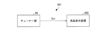
- the television receiver includes the liquid crystal display device and a tuner unit that receives a television broadcast.
- the load fluctuation of the scanning signal line driving circuit in the horizontal scanning period and the scanning in the dummy scanning period are detected.
- the load variation of the signal line driver circuit can be made equal.
- the load state of the scanning signal line drive circuit is uniform at the start of scanning of each scanning signal line and before and after that, and the charging rate between the pixels connected to the scanning signal lines that are horizontally scanned immediately after the potential polarity inversion and other pixels The difference is reduced. As a result, it is possible to suppress horizontal stripe-like unevenness that has been a problem during block inversion driving.
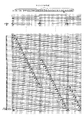
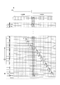
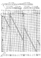
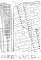
- FIG. 4 is a timing chart illustrating an example of driving of the liquid crystal display device according to the first embodiment.
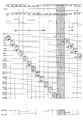
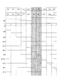
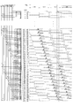
- 2 is a timing chart showing the continuation of FIG. 3 is a timing chart showing the driving example of FIGS. 1 and 2 in more detail.
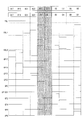
- 3 is a timing chart showing the driving example of FIGS. 1 and 2 in more detail.
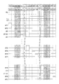
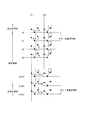
- 3 is a timing chart showing load fluctuations of the scanning signal line driving circuit in the driving example of FIGS. It is a schematic diagram which shows the structure of this liquid crystal display device.
- 6 is a schematic diagram illustrating a connection relationship between a storage capacitor line and a storage capacitor trunk line in Embodiment 1.
- FIG. 3 is a schematic diagram illustrating a polarity distribution of a write potential in Embodiment 1.
- FIG. 10 is a timing chart showing an example of driving the liquid crystal display device of FIG. 9.
- 12 is a timing chart showing another driving example of the present liquid crystal display device.
- 12 is a timing chart showing the driving example of FIG. 11 in more detail.
- 12 is a timing chart showing a load variation of the scanning signal line driving circuit in the driving example of FIG. 12 is a timing chart showing a load variation of a scanning signal line driving circuit in another driving example of the present liquid crystal display device.
- 14 is a timing chart showing still another example of driving of the present liquid crystal display device.
- 16 is a timing chart showing the driving example of FIG. 15 in more detail. 16 is a timing chart showing load fluctuations of the scanning signal line driving circuit in the driving example of FIG.
- FIG. 12 is a timing chart illustrating an example of driving of the liquid crystal display device according to the second embodiment. It is a timing chart which shows the continuation of FIG. 20 is a timing chart showing in more detail the driving example of FIGS. 6 is a schematic diagram illustrating a connection relationship between a storage capacitor line and a storage capacitor trunk line in Embodiment 2.
- FIG. 3 is a schematic diagram illustrating a polarity distribution of a write potential in Embodiment 1.
- FIG. 20 is a timing chart showing load fluctuations of the scanning signal line driving circuit in the driving example of FIGS. It is a schematic diagram which shows the other structure of this liquid crystal display device. 25 is a timing chart showing an example of driving the liquid crystal display device of FIG. FIG.
- FIG. 26 is a schematic diagram illustrating a polarity distribution of a write potential according to the driving example of FIG. 25.
- 12 is a timing chart illustrating an example of driving of the liquid crystal display device according to the third exemplary embodiment
- 10 is a timing chart illustrating another example of driving the liquid crystal display device according to the third exemplary embodiment
- 12 is a timing chart illustrating still another example of driving the liquid crystal display device according to the third exemplary embodiment
- 31 is a timing chart showing an example of driving (upstream part) in the case of FIG. 30.
- 31 is a timing chart showing an example of driving (downstream part) in the case of FIG. 30.
- It is a timing chart which shows the example of improvement of FIG.
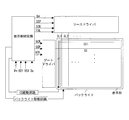
- FIG. 26 is a block diagram explaining the structure of the whole liquid crystal display device.
- FIG. 26 is a block diagram illustrating functions of the present television receiver. It is a timing chart which shows the example of a
- FIG. 6 is a schematic view showing a display unit of the present liquid crystal display device (for example, normally black mode).
- the display unit of the present liquid crystal display device is provided with scanning signal lines (G1 to G1080) and storage capacitor lines (CS1 to CS1081) parallel to the scanning signal lines, and one pixel has Two subpixels arranged in the column direction (the extending direction of the data signal line) are provided, and one pixel electrode is provided in one subpixel.
- one storage capacitor line is provided corresponding to the gap between two pixels adjacent in the column direction, and this one storage capacitor line is one of the pixel electrodes provided on one of the two pixels.
- a capacitor is formed with each of the pixel electrodes provided on the other side.
- the upper end portion and the lower end portion of the panel of the present liquid crystal display device are non-display portions, respectively, and a dummy scanning signal line G0, a dummy storage capacitor line CS0, and a dummy pixel P0 are provided at the upper end portion of the panel.
- a dummy scanning signal line G1081, a dummy storage capacitor wiring CS1082, and a dummy pixel P1081 are provided, and each subpixel is provided with two subpixels arranged in the column direction.
- One pixel electrode is provided for each pixel.
- CS1 and CS1081 are provided on both sides of the pixel column, and correspond to the gap between the pixel Pi (i is an integer from 1 to 1079) and the pixel P (i + 1).
- one storage capacitor line CS (i + 1) is provided.
- the pixel Pi (i is an integer from 1 to 1080) has two pixel electrodes connected to the scanning signal line Gi and the data signal line SL1 through transistors, and one of the pixel electrodes is a storage capacitor line CSi. And the other pixel electrode forms the storage capacitor line CS (i + 1) and the storage capacitor.
- the storage capacitor line CS1 is provided on one side (upstream side) of the pixel column, the storage capacitor line CS2 is provided corresponding to the gap between the pixel P1 and the pixel P2, and the gap between the pixel P2 and the pixel P3 is provided.
- a storage capacitor line CS3 is provided.
- the pixel P1 has two pixel electrodes connected to the scanning signal line G1 and the data signal line SL1 through transistors, and one pixel electrode forms a storage capacitor line CS1 and a storage capacitor, and the other pixel electrode. Forms a storage capacitor with the storage capacitor line CS2.
- the pixel P2 has two pixel electrodes connected to the scanning signal line G2 and the data signal line SL1 through transistors, and one pixel electrode forms a storage capacitor line CS2 and a storage capacitor, and the other The pixel electrode forms a storage capacitor with the storage capacitor line CS3.
- the dummy pixel P0 at the upper end (non-display portion) of the panel has two pixel electrodes connected to the dummy scanning signal line G0 and the data signal line SL1 through transistors, and one pixel electrode is a storage capacitor.
- the storage capacitor is formed with the wiring CS0, and the other pixel electrode forms the storage capacitor with the storage capacitor wiring CS1.
- the dummy pixel P1081 at the lower end (non-display portion) of the panel has two pixel electrodes connected to the dummy scanning signal line G1081 and the data signal line SL1 through transistors, and one pixel electrode is a storage capacitor.
- a wiring CS1081 and a storage capacitor are formed, and the other pixel electrode forms a dummy storage capacitor wiring CS1082 and a storage capacitor.
- the scanning signal lines are interlaced and scanned while the data signal lines are driven in block inversion.
- the part after the scanning signal line G1 in the display unit is considered divided into 45 blocks (B1 to B45) defined by 44 boundaries parallel to the scanning signal line.
- Each block includes 24 continuous scanning signal lines.
- the block B1 which is the most upstream block includes scanning signal lines G1 to G24
- the block B2 includes scanning signal lines G25 to G48.
- the block B3 includes scanning signal lines G49 to G72
- the block B45 which is the most downstream block includes scanning signal lines G1057 to G1080.
- G71 are grouped as Gr3, and the grouping of 24 even-numbered scanning signal lines included in the block Bj (j is an odd number from 3 to 43) and the downstream block B (j + 1), And the grouping of the odd-numbered scanning signal lines 24 included in the B (j + 1) block and the downstream block B (j + 2) is repeated to form the groups Gr4 ⁇ 45, the even-numbered scanning signal lines 12 (G1058, G1060,... G1080) included in the block B45 which is the most downstream block are set as the final group Gr46, and Gr1 to Gr46 are selected in order from the Gr1 to the selected group. Corresponding to the horizontal scanning of the scanning signal lines to which it belongs, signal potentials having the same polarity are sequentially supplied to the data signal lines.
- the data D1 to D1080 shown in FIGS. 1 and 2 are video data (digital data) corresponding to the pixels P1 to P1080 (see FIG. 3) connected to the scanning signal lines G1 to G1080, and the polarity inversion signal POL is This signal controls the polarity of the signal potential supplied to the data signal line SL1. Further, as shown in FIGS. 1 and 2, the polarity (plus / minus) of the signal potential supplied to the data signal line is inverted between the front group and the rear group selected before and after.
- the video data (D1, D3,... D23) is corresponding to the horizontal scanning of the scanning signal lines (G1, G3,... G23) belonging to the group Gr1 by selecting the group Gr1.
- the group Gr2 corresponds to sequentially supplying the corresponding positive polarity signal potential to the data signal line SL1, then selecting the group Gr2 and sequentially scanning the scanning signal lines (G2, G4... G48) belonging to the group Gr2.
- Sequentially supply a negative polarity signal potential corresponding to the video data (D2, D4,..., D48) to the data signal line SL1 then select the group Gr3 and scan signal lines (G25, G27,... Belonging to the group Gr3).
- a positive signal potential corresponding to video data (D25, D27,... D71) is sequentially applied to the data signal line SL. Supplied to. Note that a period during which a signal potential corresponding to one video data is supplied (output) to the data signal line is a horizontal scanning period (H).
- first and second dummy data are inserted between the video data corresponding to the last horizontal scan of the previous group and the video data corresponding to the first horizontal scan of the rear group, and the last horizontal scan of the previous group is also included.
- First and second dummy scanning periods are inserted between a horizontal scanning period corresponding to scanning and a horizontal scanning period corresponding to the first horizontal scanning in the subsequent group.
- the dummy scanning signal line G0 is dummy-scanned, so that the dummy scanning signal line G0 is deactivated after being activated for a predetermined period.
- a dummy potential corresponding to the first dummy data and having the same polarity as the signal potential in the subsequent group is output to the data signal line.
- the first dummy data is the same as the video data corresponding to the first horizontal scan of the rear group.
- the dummy scanning signal line 1081 is made inactive after being activated for a predetermined period.
- a dummy potential corresponding to the second dummy data and having the same polarity as the signal potential in the subsequent group is supplied to the data signal line.
- the second dummy data is the same as the video data corresponding to the first horizontal scan of the rear group.
- the timing of horizontal scanning in each horizontal scanning period is matched with the timing of dummy scanning in each dummy scanning period.
- the horizontal scanning period starts (signal potential output start) and ends (signal potential output end), and the corresponding horizontal scanning starts (writes the signal potential) and ends (signal potential)
- the dummy scanning period start (dummy potential output start) and end (dummy potential output end), and the corresponding dummy scan start (dummy potential write start) and The end (the end of writing of the dummy potential) is matched.
- the gate pulses GP1 to GP1080 supplied to the scanning signal lines G1 to G1080 and the gate pulses GP0 and GP1081 supplied to the dummy scanning signal lines G0 and G1081, respectively, have a width equal to one horizontal scanning period (1H).
- Each scanning signal line is activated simultaneously with the start of horizontal scanning corresponding to its own stage, and each dummy scanning signal line is also activated simultaneously with the start of dummy scanning corresponding to its own stage.
- the video data D23 corresponding to the last horizontal scan (G23 horizontal scan) in the group Gr1 and the first horizontal scan (G2 horizontal scan) in the group Gr2 are supported.
- the first dummy data Da and the second dummy data Db are inserted between the video data D2 and the horizontal scanning period H23 corresponding to the last horizontal scanning in the group Gr1 and the first horizontal scanning in the group Gr2.
- a first dummy scanning period DS1 and a second dummy scanning period DS2 are inserted between the corresponding horizontal scanning period H2.
- the gate pulse GP23 supplied to the scanning signal line G23 is activated simultaneously with the start of the horizontal scanning period H23, and the gate pulse GP23 is deactivated simultaneously with the end of the horizontal scanning period H23.
- a signal potential corresponding to the video data D23 (video data corresponding to a pixel connected to the scanning signal line G23) and having the same polarity (plus polarity) as the signal potential in the group Gr1 is a data signal. Supplied to the line SL1.
- the gate pulse G0 supplied to the dummy scanning signal line G0 is activated simultaneously with the start of the first dummy scanning period DS1, and the gate pulse G0 is deactivated simultaneously with the end of the first dummy scanning period DS1.
- a dummy potential corresponding to the first dummy data Da and having the same polarity (negative polarity) as the signal potential in the group Gr2 is supplied to the data signal line SL1.
- the first dummy data Da is the same as the video data D2 (data of the next frame) corresponding to the horizontal scanning immediately after the dummy scanning of the scanning signal line G2.
- the gate pulse G1081 supplied to the dummy scanning signal line G1081 is activated simultaneously with the start of the second dummy scanning period DS2, and the gate pulse G1081 is deactivated simultaneously with the end of the second dummy scanning period DS2.
- a dummy potential corresponding to the second dummy data Db and having the same polarity (negative polarity) as the signal potential in the group Gr2 is supplied to the data signal line SL1.
- the second dummy data Db is the same as the video data D2 (the data of the next frame) corresponding to the horizontal scanning immediately after the dummy scanning of the scanning signal line G2.
- the gate pulse GP2 supplied to the scanning signal line G2 is activated simultaneously with the start of the horizontal scanning period H2, and the gate pulse GP2 is deactivated simultaneously with the end of the horizontal scanning period H2.
- the signal potential corresponding to the video data D2 (video data corresponding to the pixel connected to the scanning signal line G2) and having the same polarity (negative polarity) as the signal potential in the group Gr2 is a data signal.
- the same potential is supplied to the data signal line SL1 over the first dummy scanning period DS1, the second dummy scanning period DS2, and the horizontal scanning period H2.
- the storage capacitor wiring signal SCSi supplied to the storage capacitor wiring CSi (i is an integer of 1 to 1081) and the storage capacitor wiring signals SCS0 and SCS1082 supplied to the dummy storage capacitor wirings CS0 and CS1082 will be described with reference to FIGS. This will be described with reference to FIGS.
- the storage capacitor wiring signals SCS0 to SCS1082 are 14 phases (the first phase represented by the storage capacitor wiring signal SCS1, the second phase represented by SCS2, and the third phase represented by SCS3.
- Phase 4th phase represented by SCS4, 5th phase represented by SCS5, 6th phase represented by SCS6, 7th phase represented by SCS7, 8th phase represented by SCS8, represented by SCS9 9th phase, 10th phase represented by SCS10, 11th phase represented by SCS11, 12th phase represented by SCS12, 13th phase represented by SCS13, 14th phase represented by SCS14 )
- SCS4 5th phase represented by SCS4
- 6th phase represented by SCS6 6th phase represented by SCS6, 7th phase represented by SCS7
- 10th phase represented by SCS10 11th phase represented by SCS11
- 12th phase represented by SCS12 12th phase represented by SCS12
- 13th phase represented by SCS13 14th phase represented by SCS14
- each phase has the same period (14H period consisting of a first section in which the High level continues for 7H and a second section in which the Low level continues for 7H), and the second phase represented by SCS2 is in the SCS1.
- the half phase (7H) phase is delayed from the representative first phase, and in the case of any odd-numbered phase and the next odd-numbered phase, the latter is delayed by 1H phase from the former, and any even-numbered phase In the phase and the next even-numbered phase, the latter is delayed by 1H phase from the former.
- the third phase represented by the storage capacitor wiring signal SCS3 is delayed in phase by 1H from the first phase represented by SCS1
- the fourth phase represented by SCS4 is more than the second phase represented by SCS2.
- the phase is delayed by 1H.
- the storage capacitor wiring signals SCS (28j + 1) and SCS (28k + 16) are in the first phase, j is an integer from 0 to 38, and k is from 0 to 38.
- the storage capacitor wiring signals SCS (28j + 2) and SCS (28k + 15) are in the second phase.
- the storage capacitor wiring signals SCS (28j + 3) and SCS (28k + 18) and SCS1082 are the third phase, storage capacitor wiring signal SCS (28j + 4).
- SCS (28k + 17) are the fourth phase
- the storage capacitor wiring signals SCS (28j + 5) and SCS (28k + 20) are the fifth phase
- the storage capacitor wiring signals SCS (28j + 6) and SCS (28k + 19) are the sixth phase
- the storage capacitor wiring Signals SCS (28j + 7) and SCS (28k + 22) are in the seventh phase
- storage capacitor wiring signals SCS (28j + 8) and SCS (28k + 21) are in the eighth phase
- storage capacitor wiring signals SCS (28j + 9) and SCS (28k + 24) are in the ninth phase.
- Storage capacitor wiring signals SCS (28j + 10) and SCS (28k + 23) Is the 10th phase, the storage capacitor wiring signals SCS (28j + 11) and SCS (28k + 26) are the 11th phase, the storage capacitor wiring signals SCS (28j + 12) and SCS (28k + 25) are the 12th phase, the storage capacitor wiring signal SCS0 and the storage capacitor wiring Signals SCS (28j + 13) and SCS (28k + 28) are in the 13th phase, and storage capacitor wiring signals SCS (28j + 14) and SCS (28k + 27) are in the 14th phase.
- the storage capacitor wiring signal SCS0 is in the 13th phase
- the storage capacitor wiring signal SCS1082 is in the third phase.
- these storage capacitor wiring signals SCS0 and SCS1082 do not affect the display, they can be set to arbitrary phases. .
- the first to fourteenth-phase storage capacitor wiring signals are respectively input to the storage capacitor wiring trunk wires M1 to M14, where j is an integer from 0 to 38 and k is from 0 to 38.
- the storage capacitor lines CS (28j + 1) and CS (28k + 16) are the storage capacitor trunk lines M1, j is an integer from 0 to 38, k is an integer from 0 to 38, and the storage capacitor lines CS (28j + 2) and CS (28k + 15) ) Is connected to the storage capacitor trunk wiring M2.
- the storage capacitor lines CS (28j + 3) and CS (28k + 18) and the dummy storage capacitor line CS1082 are the storage capacitor trunk line M3, storage capacitor
- the wirings CS (28j + 4) and CS (28k + 17) are the storage capacitor trunk wiring M4
- the storage capacitor wirings CS (28j + 5) and CS (28k + 20) are the storage capacitor trunk wiring M5
- the storage capacitor wirings CS (28j + 6) and CS (28k + 19) are storage.
- the capacity trunk wiring M6, the storage capacity wiring CS (28j + 7) and CS (28k + 22) are the storage capacity trunk wiring M7
- the storage capacity wiring CS (28j + 8) and CS (28k + 21) are the storage capacity trunk wiring M8, and the storage capacity wiring CS (28j + 9).
- CS (28k + 24) are the storage capacitor trunk line M9 and the storage capacitor line CS (2 j + 10) and CS (28k + 23) are the storage capacitor trunk wiring M10
- the storage capacitor wiring CS (28j + 11) and CS (28k + 26) are the storage capacitor trunk wiring M11
- the storage capacitor wiring CS (28j + 12) and CS (28k + 25) are the storage capacitor trunk wiring.
- the dummy storage capacitor line CS0 and the storage capacitor lines CS (28j + 13) and CS (28k + 28) are connected to the storage capacitor trunk line M13, and the storage capacitor lines CS (28j + 14) and CS (28k + 27) are connected to the storage capacitor trunk line M14. .
- the storage capacitor line signal SCS1 (first phase) is a horizontal signal corresponding to the scanning signal line G1.
- the level shifts from “L” to “H” after the horizontal scanning period H1 ends (for example, at the timing when 1H has elapsed from the end of H1 in FIG.
- One of the two subpixels of the pixel P1 includes a pixel electrode that forms a storage capacitor line CS1 and a storage capacitor, and the other includes a pixel electrode that forms a storage capacitor line CS2 and a storage capacitor, and A positive signal potential is supplied to these two pixel electrodes during the horizontal scanning period H1, but the holding capacitor wiring CS1 and the holding capacitor wiring CS1 are held in accordance with the level shift of the holding capacitor wiring signal SCS1 from “L” to “H”. As the potential of the pixel electrode forming the capacitor rises and the storage capacitor wiring signal SCS2 shifts from “H” to “L”, the potential of the pixel electrode forming the storage capacitor wiring CS2 and the storage capacitor decreases. .
- the effective potential Ve1 from the level shift to the elapse of one vertical scanning period is higher than the reference potential Vo (an intermediate potential between “L” and “H”, for example, the common electrode potential Vcom),
- the effective potential Ve2 from the level shift to the elapse of one vertical scanning period is lower than the reference potential Vo.
- the storage capacitor wiring signal SCS2 (second phase) is in the horizontal scanning period corresponding to the scanning signal line G2.
- the level shifts from “H” to “L” at the timing when 1H has elapsed from the end of the horizontal scanning period H2 at the “H” level to H2, and the storage capacitor wiring signal SCS3 (third phase) corresponds to the scanning signal line G2.
- the level is shifted from “L” to “H” at the timing of “L” level during the horizontal scanning period H2 and 2H from the end of the horizontal scanning period H2.
- One of the two subpixels of the pixel P2 includes a pixel electrode that forms a storage capacitor line CS2 and a storage capacitor, and the other includes a pixel electrode that forms a storage capacitor line CS3 and a storage capacitor, and Although a negative signal potential is supplied to these two pixel electrodes during the horizontal scanning period H2, the holding capacitor wiring CS2 and the holding capacitor wiring CS2 are held in accordance with the level shift of the holding capacitor wiring signal SCS2 from “H” to “L”. As the potential of the pixel electrode forming the capacitor decreases and the storage capacitor line signal SCS3 shifts from “L” to “H”, the potential of the pixel electrode forming the storage capacitor line CS3 and the storage capacitor increases. .
- the storage capacitor wiring signal SCS2 has an effective potential lower than the reference potential from the level shift until one vertical scanning period elapses
- the storage capacitor wiring signal SCS3 has the effective potential from the level shift until one vertical scanning period elapses as a reference. It is higher than the potential.
- the subpixel including the pixel electrode forming the storage capacitor wiring CS2 and the storage capacitor is defined as the “bright subpixel”, and the subpixel including the pixel electrode forming the storage capacitor wiring CS3 and the storage capacitor is displayed. “Dark sub-pixel” can be used, and halftone can be displayed by these bright / dark sub-pixels.
- the storage capacitor wiring signal SCS3 (third phase) is in the horizontal scanning period corresponding to the scanning signal line G3.
- One of the two subpixels of the pixel P3 includes a pixel electrode that forms a storage capacitor line CS3 and a storage capacitor, and the other includes a pixel electrode that forms a storage capacitor line CS4 and a storage capacitor, and A positive signal potential is supplied to these two pixel electrodes during the horizontal scanning period H3.
- the storage capacitor wiring signal SCS3 shifts from “L” to “H”
- the storage capacitor wiring CS3 and the storage electrode are held.
- the potential of the pixel electrode forming the capacitor increases and the storage capacitor line signal SCS4 shifts from “H” to “L”, the potential of the pixel electrode forming the storage capacitor line CS4 and the storage capacitor decreases. .
- the storage capacitor wiring signal SCS3 has an effective potential from the level shift until one vertical scanning period elapses higher than the reference potential
- the storage capacitor wiring signal SCS4 has the effective potential from the level shift until one vertical scanning period elapses as a reference. It is lower than the potential.
- the subpixel including the pixel electrode forming the storage capacitor line CS3 and the storage capacitor is defined as the “bright subpixel”, and the subpixel including the pixel electrode forming the storage capacitor line CS4 and the storage capacitor is displayed. “Dark sub-pixel” can be used, and halftone can be displayed by these bright / dark sub-pixels.
- two subpixels in one pixel can be displayed as “bright subpixels” and “dark subpixels”, so that halftone can be displayed. Can be increased. Furthermore, since a bright sub-pixel and a dark sub-pixel can be alternately arranged (checkered) in one pixel column, a smooth display with less roughness can be achieved.
- the polarity distribution in the column direction of the write potential to each pixel can be made dot-inverted, and flickering can be suppressed. Furthermore, compared with the case where the data signal line is driven by dot inversion (1H inversion), the power consumption and heat generation of the driver can be suppressed and the pixel charging rate can be increased. Further, immediately after the polarity of the signal potential supplied to the data signal line is inverted, a dummy potential equal to the inverted polarity is supplied to the data signal line over the first and second dummy scanning periods.
- the difference between the charging rate of the pixels connected to the first scanning signal line of the second and even-numbered blocks and the charging rate of other pixels can be reduced. Thereby, horizontal stripe-like unevenness in the vicinity of the block boundary that may be visually recognized when the block inversion drive is performed can be suppressed.
- one dummy scanning signal line is activated for a predetermined period and then deactivated, so that each scanning signal line is scanned before and at the start of scanning. This is that the load state of the scanning signal line drive circuit during scanning can be made uniform.
- a scanning signal when one scanning signal line or one dummy scanning signal line is activated and at the same time one other scanning signal line or one dummy scanning signal line is deactivated The load of the line driving circuit is Lp, and the load of the scanning signal line driving circuit when one scanning signal line or one dummy scanning signal line is active is Ly, and is located near the boundary between the blocks B1 and B2.
- the load state of the scanning signal line driving circuit before and at the start of scanning of each of the scanning signal lines G24, G25, and G26 and during scanning will be described with reference to FIG.
- one scanning signal line G22 Before the scanning of the scanning signal line G24, one scanning signal line G22 is active, so the load on the scanning signal line driving circuit is Ly, and when the scanning of the scanning signal line G24 is started, one scanning signal line G22 is activated. At the same time as the scanning signal line G24 is activated, another scanning signal line G22 is deactivated, so that the load of the scanning signal line driving circuit is Lp. During scanning of the scanning signal line G24, one scanning signal line G24 is activated. Since the scanning signal line G24 is active, the load on the scanning signal line driving circuit is Ly.
- one dummy scanning signal line G1081 is active, so the load on the scanning signal line driving circuit is Ly.
- another dummy scanning signal line G1081 is deactivated, so that the load of the scanning signal line driving circuit becomes Lp.
- the load on the scanning signal line driving circuit is Ly.
- one scanning signal line G24 is active, so the load on the scanning signal line driving circuit is Ly.
- another scanning signal line G24 is deactivated, so that the load of the scanning signal line driving circuit becomes Lp.
- one line is present. Since the scanning signal line G26 is active, the load on the scanning signal line driving circuit is Ly.
- the load fluctuation of the scanning signal line driving circuit in the horizontal scanning period and the scanning signal line driving in the dummy scanning period are detected.
- the load fluctuation of the circuit can be made equal.
- the scanning signal line driving circuit is loaded at the start of scanning and before and after scanning of each scanning signal line, and the scanning signal lines that are horizontally scanned immediately after the potential polarity inversion (the second and even-numbered blocks of the odd-numbered blocks are scanned).
- the difference in charging rate between the pixel connected to the first scanning signal line) and other pixels is reduced.
- the horizontal streak unevenness near the block boundary can be suppressed. Since the dummy scanning signal lines are provided in the non-display portion, the dummy scanning itself does not adversely affect the display.
- the load of the scanning signal line driving circuit is kept almost always Ly during the vertical scanning period, and the load variation of the scanning signal line driving circuit is hardly per se, so that it is more effective to suppress the horizontal stripe-like unevenness. It has become. Further, by making the timing when the load becomes Lp as shown in FIG. 5, it is possible to more effectively suppress the horizontal streak unevenness. Of course, as shown in FIG. 14, it is possible to adopt a configuration in which the timing (period) when the load becomes Ly and the timing when the load becomes Lp are non-periodic.
- the polarities of signal potentials supplied to two data signal lines adjacent to each other in the same horizontal scanning period or the same dummy scanning period are different from each other. For example, as shown in FIG. 4, during the period in which a positive signal potential is supplied to the data signal line SL1, a negative signal potential is supplied to the data signal line SL2, and a negative signal potential is supplied to the data signal line SL1. Is supplied to the data signal line SL2 during a period in which is supplied. In this way, the polarity distribution in the row direction of the writing potential to each pixel (the extending direction of the scanning signal line) can also be in a dot inversion as shown in FIG. 8, and flickering can be further suppressed.
- the first and second dummy data Da and Db are assumed to be the same as the video data D2 (video data of the next frame) corresponding to the horizontal scan immediately after the dummy scan of the scanning signal line G2.
- the first and second dummy data Da and Db are converted into the video data corresponding to the most recent horizontal scan before the dummy scan of the scan signal line G2 (the video data of the current frame) and the scan signal line G2 after the dummy scan. It may be determined based on video data D2 (video data of the next frame) corresponding to the latest horizontal scan.
- the first and second dummy data Da and Db may be predetermined video data (same).
- each dummy scanning period is equal to one horizontal scanning period, but the present invention is not limited to this.
- Each dummy scanning period may be shorter or longer than one horizontal scanning period.
- each dummy scanning period is shorter than one horizontal scanning period.
- the timing of horizontal scanning in each horizontal scanning period and the timing of dummy scanning in each dummy scanning period are the same.
- the storage capacitor wiring signals SCS0 to SCS2163 that are level-shifted only once in one vertical scanning period as shown in FIG. 10 may be supplied.
- the storage capacitor wiring signal SCS1 is “L” level in the horizontal scanning period H1 (the signal potential is positive polarity) corresponding to the scanning signal line G1, and “L” ⁇ 1H after the horizontal scanning period H1 ends. The level is shifted to “H”, and then the “H” level is maintained for one vertical scanning period.
- the storage capacitor wiring signal SCS2 is at the “H” level during the horizontal scanning period H1 corresponding to the scanning signal line G1, and the level is shifted from “H” to “L” at the timing when 1H has elapsed since the end of the horizontal scanning period H1. Thereafter, the “L” level is maintained for one vertical scanning period.
- the storage capacitor wiring signal SCS3 is “H” level in the horizontal scanning period H2 (signal potential is negative polarity) corresponding to the scanning signal line G2, and “H” at the timing when 1H has elapsed from the end of the horizontal scanning period H2. The level is shifted to “L”, and then the “L” level is maintained for one vertical scanning period.
- the storage capacitor wiring signal SCS4 is at the “L” level in the horizontal scanning period H2 corresponding to the scanning signal line G2, and is shifted in level from “L” to “H” at the timing when 1H has elapsed from the end of the horizontal scanning period H2. Thereafter, the “H” level is maintained for one vertical scanning period.
- the storage capacitor wiring signal SCS5 is “L” level in the horizontal scanning period H3 (the signal potential is positive polarity) corresponding to the scanning signal line G3, and “L” ⁇ 1H after the horizontal scanning period H3 ends. The level is shifted to “H”, and then the “H” level is maintained for one vertical scanning period.
- the storage capacitor wiring signal SCS6 is at the “H” level in the horizontal scanning period H3 corresponding to the scanning signal line G3, and is shifted in level from “H” to “L” at the timing when 1H has elapsed from the end of the horizontal scanning period H3. Thereafter, the “L” level is maintained for one vertical scanning period.
- halftone can be displayed with two subpixels in one pixel as “bright subpixels” and “dark subpixels”, so that viewing angle characteristics can be improved.
- a bright sub-pixel and a dark sub-pixel can be alternately arranged (checkered) in one pixel column, a smooth display with less roughness can be achieved.
- dummy scanning signal line G0 is dummy scanned during the first dummy scanning period, and another dummy scanning signal line G1081 is dummy scanned during the second dummy scanning period. It is not limited to this.
- the dummy scanning signal line G0 may be subjected to dummy scanning over the first to second dummy scanning periods. In other words, the scanning signal line G0 is activated at the start of the first dummy scanning period and deactivated at the end of the second dummy scanning period.
- the gate pulses GP1 to GP1080 and the storage capacitor wiring signals SCS0 to SCS1082 supplied to the scanning signal lines G1 to G1080 are the same as those shown in FIGS.
- the gate pulse G0 supplied to the dummy scanning signal line G0 is activated simultaneously with the start of the first dummy scanning period DS1, and the gate pulse G0 is deactivated simultaneously with the end of the second dummy scanning period DS2.
- a dummy potential corresponding to the first dummy data Da and having the same polarity (negative polarity) as the signal potential in the group Gr2 is supplied to the data signal line SL1
- one scanning signal line or one dummy scanning signal line is activated, and at the same time, another scanning signal line or one dummy scanning signal line is inactive.
- the load of the scanning signal line drive circuit at the time of conversion is Lp
- the load of the scanning signal line drive circuit when one scanning signal line or one dummy scanning signal line is active is Ly.
- FIG. 13 it is possible to make the load state of the scanning signal line driving circuit uniform before and at the start of scanning of each scanning signal line and during scanning. As a result, the difference between the charging rate of the pixels connected to the second scanning signal line of the odd-numbered block and the first scanning signal line of the even-numbered block and the charging rate of the other pixels can be reduced. The unevenness of the shape can be suppressed.
- the gate pulses GP0 to GP1081 are pulses whose width is equal to twice (2H) of one horizontal scanning period, and each scanning signal line corresponds to the horizontal corresponding to its own stage.
- the horizontal scanning timing in each horizontal scanning period is matched with the dummy scanning timing in each dummy scanning period.
- the horizontal scanning period starts (signal potential output start) and ends (signal potential output end), and the corresponding horizontal scanning starts (writes the signal potential) and ends (signal potential)
- the dummy scanning period start (dummy potential output start) and end (dummy potential output end), and the corresponding dummy scan start (dummy potential write start) and The end (the end of writing of the dummy potential) is matched.
- the storage capacitor wiring signals SCS0 to 1082 are the same as those shown in FIGS.
- the gate pulse GP23 supplied to the scanning signal line G23 is activated simultaneously with the start of the horizontal scanning immediately before the horizontal scanning corresponding to the scanning signal line G23, that is, simultaneously with the start of the horizontal scanning period H21. It becomes active for two horizontal scanning periods of the scanning period H23, and becomes inactive simultaneously with the end of the horizontal scanning period H23.
- the signal potential corresponding to the video data D21 (video data corresponding to the pixel connected to the scanning signal line G21) and having the same polarity (plus polarity) as the signal potential in the group Gr1 is a data signal. Supplied to the line SL1.
- a signal potential having the same polarity (plus polarity) as the signal potential in the group Gr1 corresponds to the video data D23 (video data corresponding to the pixel connected to the scanning signal line G23). It is supplied to the data signal line SL1. That is, precharging is performed in the horizontal scanning period H21, and main charging (writing of a positive polarity signal potential corresponding to the video data D23) is performed in the horizontal scanning in the horizontal scanning period H23.
- the gate pulse GP0 supplied to the scanning signal line G0 is activated simultaneously with the start of the horizontal scanning immediately before the dummy scanning corresponding to the dummy scanning signal line G0, that is, at the start of the horizontal scanning period H23. It becomes active for two horizontal scanning periods of one dummy scanning period DS1, and becomes inactive simultaneously with the end of the first dummy scanning period DS1.
- the gate pulse GP1081 supplied to the scanning signal line G1081 is activated simultaneously with the start of the dummy scanning immediately before the dummy scanning corresponding to the dummy scanning signal line G1080, that is, at the start of the first dummy scanning period DS1, and the first dummy scanning is performed. It becomes active for two horizontal scanning periods of the period DS1 and the second dummy scanning period DS2, and is deactivated simultaneously with the end of the second dummy scanning period DS2.
- the gate pulse GP2 supplied to the scanning signal line G2 is activated simultaneously with the start of the dummy scanning immediately before the horizontal scanning corresponding to the scanning signal line G2, that is, the second dummy scanning period DS2, and the second dummy scanning period. It becomes active for two horizontal scanning periods of DS2 and horizontal scanning period H2, and becomes inactive simultaneously with the end of horizontal scanning period H2.
- a signal potential having the same polarity (negative polarity) as the signal potential in the group Gr2 corresponding to the second dummy data Db is supplied to the data signal line SL1.
- a signal potential corresponding to the video data D2 (video data corresponding to a pixel connected to the scanning signal line G2) and having the same polarity (plus polarity) as the signal potential in the group Gr2 is a data signal. Supplied to the line SL1. That is, precharging is performed in the dummy scanning period DS2, and main charging (writing of a positive polarity signal potential corresponding to the video data D2) is performed in the horizontal scanning in the horizontal scanning period H2.
- one scanning signal line or one dummy scanning signal line is in an active state, and another scanning signal line or one dummy scanning signal line is activated simultaneously with another scanning signal line or another dummy scanning signal line.
- the load of the scanning signal line driving circuit when one scanning signal line or one dummy scanning signal line is deactivated is different from Lq, one scanning signal line, or one dummy scanning signal line.
- the scanning signal line drive circuit load when the one scanning signal line or one dummy scanning signal line is active is set to Lz, and scanning signal lines G24 and G25 located in the vicinity of the boundary between the blocks B1 and B2
- the load state of the scanning signal line driving circuit before and at the start of scanning of G26 and during scanning will be described with reference to FIG.
- one scanning signal line G22 and one scanning signal line G24 are active, so the load of the scanning signal line driving circuit is Lz, and the scanning of the scanning signal line G24 is performed.
- one scanning signal line G24 is in an active state, and another scanning signal line G26 is activated at the same time as another scanning signal line G22 is deactivated.
- the load of the line drive circuit is Lq.
- the load of the scanning signal line driving circuit is Lz.
- one dummy scanning signal line G0 and one dummy scanning signal line G1081 are active, so the load of the scanning signal line driving circuit is Lz, and the scanning signal line G25.
- the load of the scanning signal line driving circuit is Lq.
- the load of the scanning signal line driving circuit is Lz.
- one scanning signal line G24 and one scanning signal line G26 are active, so the load of the scanning signal line driving circuit is Lz, and the scanning of the scanning signal line G26 is performed.
- one scanning signal line G26 is active, and another scanning signal line G28 is activated at the same time, and another scanning signal line G24 is deactivated.
- the load of the line drive circuit is Lq.
- the load on the scanning signal line driving circuit is Lz.
- the load state of the scanning signal line driving circuit can be made uniform before the scanning of each scanning signal line, at the start of scanning, and during the scanning.
- the difference between the charging rate of the pixels connected to the second scanning signal line of the odd-numbered block and the first scanning signal line of the even-numbered block and the charging rate of the other pixels can be reduced.
- the unevenness of the shape can be suppressed.
- the load of the scanning signal line driving circuit is kept almost always Lz during the vertical scanning period, and there is almost no load fluctuation of the scanning signal line driving circuit. ing.
- the horizontal streak unevenness can be more effectively suppressed by periodically setting the timing at which the load becomes Lq.
- each pixel is precharged for one horizontal period, so the charge rate of each pixel can be increased.
- each dummy scanning period is equal to one horizontal scanning period, but the present invention is not limited to this.
- Each dummy scanning period may be shorter or longer than one horizontal scanning period.
- the scanning signal lines are sequentially scanned while the data signal lines are driven by block inversion.
- the part after the scanning signal line G1 in the display unit is divided into 90 blocks (B1 to B90) defined by 89 boundaries parallel to the scanning signal line.
- Each block includes 12 continuous scanning signal lines.
- the block B1 which is the most upstream block includes scanning signal lines G1 to G12
- the block B2 includes scanning signal lines G13 to G24.
- the block B3 includes scanning signal lines G25 to G36
- the block B90 which is the most downstream block includes scanning signal lines G1069 to G1080.
- 12 scanning signal lines (G1, G2,... G12) included in the block B1, which is the most upstream block, are set as the first group Gr1
- 12 scanning signal lines included in the block B2 on the downstream side of the block B1 G13, G14,..., G24
- 12 scanning signal lines included in each block are set as groups Gr3 to Gr90 in order
- scanning signal lines belonging to the selected group are selected from Gr1 to Gr90 in order.
- the polarity inversion signal POL in FIGS. 24 and 25 the polarity (plus / minus) of the signal potential supplied to the data signal line is inverted between the front group and the rear group selected before and after.
- the video data (D1, D2,... D12) is corresponding to the horizontal scanning of the scanning signal lines (G1, G2,... G12) belonging to the group Gr1 by selecting the group Gr1.
- the group Gr2 corresponds to sequentially supplying the corresponding positive polarity signal potential to the data signal line SL1, and then selecting the group Gr2 and sequentially scanning the scanning signal lines (G13, G14... G24) belonging to the group Gr2.
- a negative polarity signal potential corresponding to the video data (D13, D14... D24) is sequentially supplied to the data signal line SL1, and then the group Gr3 is selected and the scanning signal lines (G25, G26,...
- a positive polarity signal potential corresponding to the video data (D25, D26... D48) is sequentially transmitted. It is supplied to the line SL1. Note that a period during which a signal potential corresponding to one video data is supplied (output) to the data signal line is a horizontal scanning period (H).
- first and second dummy data are inserted between the video data corresponding to the last horizontal scan of the previous group and the video data corresponding to the first horizontal scan of the rear group, and the last horizontal scan of the previous group
- First and second dummy scanning periods are inserted between a horizontal scanning period corresponding to scanning and a horizontal scanning period corresponding to the first horizontal scanning in the subsequent group.
- the dummy scanning signal line G0 is dummy-scanned, so that the dummy scanning signal line G0 is deactivated after being activated for a predetermined period.
- a dummy potential corresponding to the first dummy data and having the same polarity as the signal potential in the subsequent group is output to the data signal line.
- the first dummy data is the same as the video data corresponding to the first horizontal scan of the rear group.
- the dummy scanning signal line 1081 is made inactive after being activated for a predetermined period.
- a dummy potential corresponding to the second dummy data and having the same polarity as the signal potential in the subsequent group is supplied to the data signal line.
- the second dummy data is the same as the video data corresponding to the first horizontal scan of the rear group.
- the timing of horizontal scanning in each horizontal scanning period is matched with the timing of dummy scanning in each dummy scanning period.
- the horizontal scanning period starts (signal potential output start) and ends (signal potential output end), and the corresponding horizontal scanning starts (writes the signal potential) and ends (signal potential)
- the dummy scanning period start (dummy potential output start) and end (dummy potential output end), and the corresponding dummy scan start (dummy potential write start) and The end (the end of writing of the dummy potential) is matched.
- the gate pulses GP1 to GP1080 supplied to the scanning signal lines G1 to G1080 and the gate pulses GP0 and GP1081 supplied to the dummy scanning signal lines G0 and G1081, respectively, have a width equal to one horizontal scanning period (1H).
- Each scanning signal line is activated simultaneously with the start of horizontal scanning corresponding to its own stage, and each dummy scanning signal line is also activated simultaneously with the start of dummy scanning corresponding to its own stage.
- FIGS. 18 and 19 it corresponds to the video data D12 corresponding to the last horizontal scan (G12 horizontal scan) in the group Gr1 and the first horizontal scan (G13 horizontal scan) in the group Gr2.
- the first dummy data Da and the second dummy data Db are inserted between the video data D13 and the horizontal scanning period H12 corresponding to the last horizontal scanning in the group Gr1 and the first horizontal scanning in the group Gr2.
- a first dummy scanning period DS1 and a second dummy scanning period DS2 are inserted between the corresponding horizontal scanning period H13.
- the gate pulse GP12 supplied to the scanning signal line G12 is activated simultaneously with the start of the horizontal scanning period H12, and the gate pulse GP12 is deactivated simultaneously with the end of the horizontal scanning period H12.
- the signal potential corresponding to the video data D12 (video data corresponding to the pixel connected to the scanning signal line G12) and having the same polarity (plus polarity) as the signal potential in the group Gr1 is a data signal. Supplied to the line SL1.
- the gate pulse G0 supplied to the dummy scanning signal line G0 is activated simultaneously with the start of the first dummy scanning period DS1, and the gate pulse G0 is deactivated simultaneously with the end of the first dummy scanning period DS1.
- a dummy potential corresponding to the first dummy data Da and having the same polarity (negative polarity) as the signal potential in the group Gr2 is supplied to the data signal line SL1.
- the first dummy data Da is the same as the video data D13 (data of the next frame) corresponding to the horizontal scanning immediately after the dummy scanning of the scanning signal line G2.
- the gate pulse G1081 supplied to the dummy scanning signal line G1081 is activated simultaneously with the start of the second dummy scanning period DS2, and the gate pulse G1081 is deactivated simultaneously with the end of the second dummy scanning period DS2.
- a dummy potential corresponding to the second dummy data Db and having the same polarity (negative polarity) as the signal potential in the group Gr2 is supplied to the data signal line SL1.
- the second dummy data Db is the same as the video data D13 (data of the next frame) corresponding to the horizontal scanning immediately after the dummy scanning of the scanning signal line G2.
- the gate pulse GP13 supplied to the scanning signal line G13 is activated simultaneously with the start of the horizontal scanning period H13, and the gate pulse GP13 is deactivated simultaneously with the end of the horizontal scanning period H13.
- the signal potential corresponding to the video data D13 (video data corresponding to the pixel connected to the scanning signal line G13) and having the same polarity (negative polarity) as the signal potential in the group Gr2 is a data signal.
- the same potential is supplied to the data signal line SL1 over the first dummy scanning period DS1, the second dummy scanning period DS2, and the horizontal scanning period H13.
- the storage capacitor wiring signal SCSi supplied to the storage capacitor wiring CSi (i is an integer from 1 to 1081) and the storage capacitor wiring signals SCS0 and SCS1082 supplied to the dummy storage capacitor wirings CS0 and CS1082. It explains using.
- the storage capacitor wiring signals SCS0 to SCS1082 are represented by 11 phases (the first phase represented by the storage capacitor wiring signal SCS2, the second phase represented by SCS1 and 3 and the SCS4).
- 3rd phase 4th phase represented by SCS5, 5th phase represented by SCS6, 6th phase represented by SCS7, 7th phase represented by SCS8, 8th phase represented by SCS9, SCS10 Or the waveform of the ninth phase represented by SCS11, the tenth phase represented by SCS12).
- each phase has the same period (28H period consisting of the first section in which the High level continues for 14H and the second section in which the Low level continues for 14H), and the second phase represented by SCS1 is in SCS2.
- the 16H phase is delayed from the representative first phase, and the arbitrary odd-numbered phase and the next odd-numbered phase in the latter are 2H-phase later than the former, the arbitrary even-numbered phase and the next In the even-numbered phase, the latter is delayed by 2H phase than the former.
- the third phase represented by SCS4 is delayed in phase by 2H from the first phase represented by SCS2, and the fourth phase represented by SCS5 is 2H more in phase than the second phase represented by SCS3. Running late.
- the storage capacitor wiring signal SCS (12j + 2) and SCS0 / SCS1082 are in the first phase
- the storage capacitor wiring signal SCS1 and SCS (12j + 3) are in the second phase
- the storage capacitor wiring signal SCS (12j + 4 Is the third phase
- the storage capacitor wiring signal SCS (12j + 5) is the fourth phase
- the storage capacitor wiring signal SCS (12j + 6) is the fifth phase
- the storage capacitor wiring signal SCS (12j + 7) is the sixth phase
- the storage capacitor wiring signal SCS (12j + 8) is in the seventh phase
- the storage capacitor wiring signal SCS (12j + 9) is in the eighth phase
- the storage capacitor wiring signal SCS (12j + 10) is in the ninth phase.
- j is an integer from 0 to 89
- k is an integer from 0 to 89
- the storage capacitor wiring signals SCS (12j + 11) and SCS (12k + 13) are in the tenth phase.
- the storage capacitor wiring signal SCS (12j + 12) is in the eleventh phase.
- the first to eleventh-phase storage capacitor wiring signals are respectively input to the storage capacitor wiring trunk wires M1 to M11, and j is an integer from 0 to 89, and the storage capacitor wires SCS0.
- the SCS 1082 and SCS (12j + 2) are connected to the storage capacitor trunk wiring M1
- the storage capacitor wirings CS1 and CS (12j + 3) are connected to the storage capacitor trunk wiring M2
- the storage capacitor wiring CS (12j + 4) is connected to the storage capacitor trunk wiring M3, and the storage capacitor wiring CS.
- the storage capacitor wiring CS (12j + 5) is stored in the storage capacitor trunk wiring M4, storage capacitor wiring CS (12j + 6) is stored in the storage capacitor trunk wiring M5, storage capacitor wiring CS (12j + 7) is stored in the storage capacitor trunk wiring M6, and storage capacitor wiring CS (12j + 8) is stored.
- the storage capacity wiring CS (12j + 9) is in the storage capacity trunk wiring M8, and the storage capacity wiring CS (12j + 10) is in the storage capacity trunk wiring M9. It is connected.
- the storage capacitor lines CS (12j + 11) and CS (12k + 13) are connected to the storage capacitor trunk line M10, where j is an integer from 0 to 89 and k is an integer from 0 to 89.
- the storage capacitor line CS (12j + 12) is connected to the storage capacitor trunk line M11, where j is an integer of 0 to 89.
- the storage capacitor line signal SCS1 (second phase) is a horizontal signal corresponding to the scanning signal line G1.
- the level shifts from “L” to “H” at the “L” level in the scanning period H1 and 4H from the end of the horizontal scanning period H1, and the storage capacitor wiring signal SCS2 (first phase) is shifted to the scanning signal line G1.
- the level is set to be “H” level in the horizontal scanning period H1 corresponding to “H” and level shifted from “H” to “L” at the timing when 2H has elapsed since the end of the horizontal scanning period H1.
- One of the two subpixels of the pixel P1 includes a pixel electrode that forms a storage capacitor line CS1 and a storage capacitor, and the other includes a pixel electrode that forms a storage capacitor line CS2 and a storage capacitor, and A positive signal potential is supplied to these two pixel electrodes during the horizontal scanning period H1, but the holding capacitor wiring CS1 and the holding capacitor wiring CS1 are held in accordance with the level shift of the holding capacitor wiring signal SCS1 from “L” to “H”. As the potential of the pixel electrode forming the capacitor rises and the storage capacitor wiring signal SCS2 shifts from “H” to “L”, the potential of the pixel electrode forming the storage capacitor wiring CS2 and the storage capacitor decreases. .
- the storage capacitor wiring signal SCS1 has a higher effective potential than the reference potential from the level shift until one vertical scanning period elapses
- the storage capacitor wiring signal SCS2 has the effective potential from the level shift until one vertical scanning period elapses as a reference. It is lower than the potential.
- the subpixel including the storage capacitor line CS1 and the pixel electrode that forms the storage capacitor is defined as the “bright subpixel”, and the subpixel including the storage capacitor line CS2 and the pixel electrode that forms the storage capacitor is displayed. “Dark sub-pixel” can be used, and halftone can be displayed by these bright / dark sub-pixels.
- the storage capacitor wiring signal SCS2 (first and second phases) is in the horizontal scanning period corresponding to the scanning signal line G2.
- One of the two subpixels of the pixel P2 includes a pixel electrode that forms a storage capacitor line CS2 and a storage capacitor, and the other includes a pixel electrode that forms a storage capacitor line CS3 and a storage capacitor, and A positive signal potential is supplied to these two pixel electrodes during the horizontal scanning period H1, but the holding capacitor line CS2 and the holding capacitor line CS2 are held in accordance with the level shift of the holding capacitor line signal SCS2 from “H” to “L”. As the potential of the pixel electrode forming the capacitor decreases and the storage capacitor line signal SCS3 shifts from “L” to “H”, the potential of the pixel electrode forming the storage capacitor line CS3 and the storage capacitor increases. .
- the storage capacitor wiring signal SCS2 has an effective potential lower than the reference potential from the level shift until one vertical scanning period elapses
- the storage capacitor wiring signal SCS3 has the effective potential from the level shift until one vertical scanning period elapses as a reference. It is higher than the potential.
- the sub-pixel including the storage capacitor wiring CS2 and the pixel electrode that forms the storage capacitor is referred to as the “dark sub-pixel”
- the sub-pixel including the storage capacitor wiring CS3 and the pixel electrode that forms the storage capacitor is replaced. “Bright subpixels” can be used, and halftones can be displayed by these bright and dark subpixels.
- the storage capacitor wiring signal SCS13 (tenth phase) is in the horizontal scanning period corresponding to the scanning signal line G13.
- One of the two sub-pixels of the pixel P13 includes a pixel electrode that forms a storage capacitor with the storage capacitor line CS13, and the other includes a pixel electrode that forms a storage capacitor with the storage capacitor line CS14, and These two pixel electrodes are supplied with a negative signal potential in the horizontal scanning period H13.
- the storage capacitor wiring signal SCS13 is level-shifted from “H” to “L”
- the storage capacitor wiring CS13 and the storage electrode are held.
- the potential of the pixel electrode forming the capacitor decreases and the storage capacitor line signal SCS14 shifts from “L” to “H”, the potential of the pixel electrode forming the storage capacitor line CS14 and the storage capacitor increases. .
- the storage capacitor line signal SCS13 has an effective potential lower than the reference potential from the level shift until one vertical scanning period elapses
- the storage capacitor line signal SCS14 has the effective potential from the level shift until one vertical scanning period elapses as the reference potential. It is higher than the potential.
- the subpixel including the storage capacitor line CS13 and the pixel electrode forming the storage capacitor is referred to as a “bright subpixel”
- the subpixel including the storage capacitor line CS14 and the pixel electrode forming the storage capacitor is referred to as a “dark subpixel”.
- halftones can be displayed by these bright / dark sub-pixels.
- two subpixels in one pixel can be displayed as “bright subpixels” and “dark subpixels”, so that a halftone can be displayed.
- the characteristics can be enhanced.
- the power consumption and heat generation of the driver can be suppressed and the pixel charging rate can be increased as compared with the case where the data signal line is driven by dot inversion (1H inversion). Further, immediately after the polarity of the signal potential supplied to the data signal line is inverted, a dummy potential equal to the inverted polarity is supplied to the data signal line over the first and second dummy scanning periods. The difference between the charging rate of the pixels connected to the first scanning signal line of the second and even-numbered blocks and the charging rate of other pixels can be reduced. Thereby, horizontal stripe-like unevenness in the vicinity of the block boundary that may be visually recognized when the block inversion drive is performed can be suppressed.
- one dummy scanning signal line is activated for a predetermined period and then deactivated, so that each scanning signal line is scanned before and at the start of scanning. This is that the load state of the scanning signal line drive circuit during scanning can be made uniform.
- a scanning signal when one scanning signal line or one dummy scanning signal line is activated and at the same time one other scanning signal line or one dummy scanning signal line is deactivated The load of the line driving circuit is Lp, and the load of the scanning signal line driving circuit when one scanning signal line or one dummy scanning signal line is active is Ly, and is located near the boundary between the blocks B1 and B2.
- the load state of the scanning signal line driving circuit before and at the start of scanning of each of the scanning signal lines G12, G13, and G14 and during the scanning will be described with reference to FIG.
- one scanning signal line G11 Before the scanning of the scanning signal line G12, one scanning signal line G11 is active, so the load of the scanning signal line driving circuit is Ly, and at the start of scanning of the scanning signal line G12, one scanning signal line G11 is activated. At the same time as the scanning signal line G12 is activated, another scanning signal line G11 is deactivated, so that the load of the scanning signal line driving circuit is Lp, and one scanning signal line G12 is scanned during scanning. Since the scanning signal line G12 is active, the load on the scanning signal line driving circuit is Ly.
- one dummy scanning signal line G1081 is active, so the load on the scanning signal line driving circuit is Ly.
- another dummy scanning signal line G1081 is deactivated, so that the load of the scanning signal line driving circuit becomes Lp.
- the load on the scanning signal line driving circuit is Ly.
- one scanning signal line G13 Before the scanning of the scanning signal line G14, one scanning signal line G13 is active, so the load of the scanning signal line driving circuit is Ly. At the same time that the scanning signal line G14 is activated, another scanning signal line G13 other than this is deactivated, so the load of the scanning signal line driving circuit becomes Lp, and one scanning signal line G14 is scanned during scanning. Since the scanning signal line G14 is active, the load on the scanning signal line driving circuit is Ly.
- the load state of the scanning signal line driving circuit can be made uniform before the scanning of each scanning signal line, at the start of scanning, and during the scanning.
- the difference between the charging rate of the pixel connected to the scanning signal line at the head of the block and the charging rate of the other pixels can be reduced, and the horizontal streak unevenness near the block boundary can be suppressed.
- the load of the scanning signal line driving circuit is kept almost always Ly during the vertical scanning period, and the load variation of the scanning signal line driving circuit is hardly per se, so that it is more effective to suppress the horizontal stripe-like unevenness. It has become.
- FIG. 23 by making the timing when the load becomes Lp periodic, it is possible to more effectively suppress the horizontal streak-like unevenness. It is also possible to adopt a form in which the timing (period) when the load becomes Ly and the timing when the load becomes Lp are non-periodic.
- the scanning of the data signal line is skipped while the data signal line is driven to invert the block.
- the liquid crystal display device of FIG. 24 the liquid crystal display device of FIG.
- the scanning signal lines are sequentially scanned while the data signal lines are driven by block inversion, but the invention is not limited to these.
- the scanning signal lines may be skipped while the data signal lines are driven by block inversion as shown in FIG. 25. In this case, the display shown in FIG. It becomes.
- the liquid crystal display device (non-multi-pixel method) shown in FIG. 24 it is also possible to sequentially scan the scanning signal lines while driving the data signal lines in a block inversion manner.
- the liquid crystal display device shown in FIG. 6 can also be driven as shown in FIG. That is, the storage capacitor wiring signals SCS0 to SCS1082 have any of 12-phase waveforms (first to twelfth phases represented by the storage capacitor wiring signals SCS1 to SCS12).
- the first section where the low level continues for 6H the second section where the high level continues for 8H, the third section where the low level continues for 8H, and the fourth section where the high level continues for 6H.
- the reference waveform is repeated.
- the first section in which the High level continues for 6H the second section in which the Low level continues for 8H
- the third section in which the High level continues for 8H the fourth section in which the Low level continues for 6H.
- the reference waveform consisting of is repeated.
- the second phase represented by SCS2 is an inversion of the first phase represented by SCS1, and the latter is greater than the former in any odd-numbered phase and the next odd-numbered phase.
- the 1H phase is delayed, and in any even-numbered phase and the next even-numbered phase, the latter is delayed by 1H phase than the former.
- the third phase represented by the storage capacitor wiring signal SCS3 is delayed in phase by 1H from the first phase represented by SCS1
- the fourth phase represented by SCS4 is more than the second phase represented by SCS2.
- the phase is delayed by 1H.
- the storage capacitor wiring signals SCS (24j + 1) and SCS (24k + 14) are in the first phase, where j is an integer from 0 to 45 and k is an integer from 0 to 44. Further, assuming that j is an integer from 0 to 45 and k is an integer from 0 to 44, the storage capacitor wiring signals SCS (24j + 2) and SCS (24k + 13) and SCS1082 are the second phase, the storage capacitor wiring signals SCS (24j + 3) and SCS ( 24k + 16) is the third phase, the storage capacitor wiring signals SCS (24j + 4) and SCS (24k + 15) are the fourth phase, the storage capacitor wiring signals SCS (24j + 5) and SCS (24k + 18) are the fifth phase, and the storage capacitor wiring signal SCS (24j + 6).
- SCS (24k + 17) are in the sixth phase
- the storage capacitor wiring signals SCS (24j + 7) and SCS (24k + 20) are in the seventh phase
- the storage capacitor wiring signals SCS (24j + 8) and SCS (24k + 19) are in the eighth phase
- the storage capacitor wiring Signals SCS (24j + 9) and SCS (24k + 22) Capacitance wiring signals SCS (24j + 10) and SCS (24k + 21) are in the 10th phase
- storage capacitance wiring signals SCS (24j + 11) and SCS (24k + 24) and SCS0 are in the 11th phase
- storage capacitance wiring signals SCS (24j + 12) and SCS (24k + 23) Is in the 12th phase.
- the first to twelfth-phase storage capacitor wiring signals are input to the storage capacitor wiring trunk wires M1 to M12, respectively.
- a timing adjustment scanning period is inserted in addition to the dummy scanning period. That is, the first and second dummy data are inserted between the video data corresponding to the last horizontal scan of the previous group and the video data corresponding to the first horizontal scan of the rear group, and the last horizontal scan of the previous group First and second dummy scanning periods are inserted between the horizontal scanning period corresponding to scanning and the horizontal scanning period corresponding to the first horizontal scanning in the subsequent group, and in addition, m is an integer from 0 to 42, First and second timing adjustment data are inserted between the video data corresponding to the horizontal scanning of the scanning signal line G (25m + 11) and the video data corresponding to the horizontal scanning of the scanning signal line G (25m + 13), and the scanning signal Two timings are provided between a horizontal scanning period corresponding to the horizontal scanning of the line G (25m + 11) and a horizontal scanning period corresponding to the horizontal scanning of the scanning signal line G (25m + 13).
- the first timing adjustment data is, for example, the same as the video data corresponding to the horizontal scanning of the scanning signal line G (25m + 13), and the second timing adjustment data is, for example, the horizontal scanning of the scanning signal line G (25m + 15). Same as the corresponding video data.
- the dummy scanning signal line G0 is dummy-scanned, so that the dummy scanning signal line G0 is deactivated after being activated for a predetermined period.
- a dummy potential corresponding to the first dummy data and having the same polarity as the signal potential in the subsequent group is output to the data signal line.
- the dummy scanning signal line 1081 is made inactive after being activated for a predetermined period.
- a dummy potential corresponding to the second dummy data and having the same polarity as the signal potential in the subsequent group is supplied to the data signal line.
- the horizontal scanning timing in each horizontal scanning period is matched with the dummy scanning timing in each dummy scanning period.
- the dummy scanning signal line G0 is subjected to timing adjustment scanning, so that the dummy scanning signal line G0 is made inactive after being activated for a predetermined period.
- a potential corresponding to the first timing adjustment data is output to the data signal line.
- the dummy scanning signal line G1081 is subjected to timing adjustment scanning, so that the dummy scanning signal line 1081 is made inactive after being activated for a predetermined period.
- a potential corresponding to the second timing adjustment data is supplied to the data signal line.
- the horizontal scanning timing in each horizontal scanning period and the timing adjustment scanning timing in each timing adjustment scanning period are made to coincide.
- the storage capacitor wiring signal SCS1 (first phase) is at the “L” level of the first section in the horizontal scanning period H1 corresponding to the scanning signal line G1, and is synchronized with the end of the horizontal scanning period H1. Then, the level shifts from “L” to “H” to start the second section, and the storage capacitor wiring signal SCS2 (second phase) is “H” in the first section in the horizontal scanning period H1 corresponding to the scanning signal line G1. The level is set so that the second section starts with a level shift from “H” to “L” in synchronization with the end of the horizontal scanning period H1.
- the storage capacitor wiring signal SCS1 (first phase) is at the “L” level of the first section in the horizontal scanning period H1 corresponding to the scanning signal line G1, and from the end of the horizontal scanning period H1. Level 2 is shifted from “L” to “H” at the timing when 2H elapses, and the second section starts.
- the storage capacitor wiring signal SCS2 (second phase) is changed to the first section in the horizontal scanning period H1 corresponding to the scanning signal line G1. At the “H” level, the level is shifted from “H” to “L” at the timing when 2H elapses from the end of the horizontal scanning period H1, and the second section starts.
- the driving of FIG. 27 is modified, and in the odd-numbered phase, the first section in which the Low level continues for 6H, the second section in which the High level continues for 1H, and the third section in which the Low level continues for 1H.
- Section 4 the 4th section where the High level continues for 6H, the 5th section where the Low level continues for 1H, the 6th section where the High level continues for 1H, the 7th section where the Low level continues for 6H, and the 8th section where the High level continues for 6H
- the first section in which the High level continues for 6H, the second section in which the Low level continues for 1H, the third section in which the High level continues for 1H, and the Low level of 6H are repeated.
- the reference waveform is composed of the following 4th section, the 5th section where the High level continues for 1H, the 6th section where the Low level continues for 1H, the 7th section where the High level continues for 6H, and the 8th section where the Low level continues for 6H. Repeated It is also possible to so that.
- the storage capacitor wiring signal SCS1 (first phase) is at the “L” level of the first section in the horizontal scanning period H1 corresponding to the scanning signal line G1, and is synchronized with the end of the horizontal scanning period H1. Then, the level shifts from “L” to “H” to start the second section, and the storage capacitor wiring signal SCS2 (second phase) is “H” in the first section in the horizontal scanning period H1 corresponding to the scanning signal line G1. The level is set so that the second section starts with a level shift from “H” to “L” in synchronization with the end of the horizontal scanning period H1.
- the first and second dummy scanning periods are inserted between the horizontal scanning period corresponding to the last horizontal scanning in the previous group and the horizontal scanning period corresponding to the first horizontal scanning in the subsequent group.
- the dummy scanning signal line G0 is deactivated after being activated for a predetermined period
- the dummy scanning signal line G1081 is dummy scanned.
- the dummy scanning signal line 1081 is deactivated after being activated for a predetermined period.
- j is an integer of 0 to 10
- two timing adjustment scans are performed between the horizontal scanning period corresponding to the scanning signal line G (96j + 23) and the horizontal scanning period corresponding to the scanning signal line G (96j + 25).
- a period (first and second timing adjustment scanning periods) is inserted, and the dummy scanning signal line G0 is activated for a predetermined period by performing timing adjustment scanning of the dummy scanning signal line G0 in the first timing adjustment scanning period.
- the dummy scanning signal line G1081 is deactivated later, and the dummy scanning signal line G1081 is subjected to timing adjustment scanning in the second timing adjustment scanning period, so that the dummy scanning signal line G1081 is deactivated after being activated for a predetermined period.
- two timing adjustment scans are performed between the horizontal scanning period corresponding to the scanning signal line G (96k + 72) and the horizontal scanning period corresponding to the scanning signal line G (96k + 74).
- a period (first and second timing adjustment scanning periods) is inserted, and the dummy scanning signal line G0 is activated for a predetermined period by performing timing adjustment scanning of the dummy scanning signal line G0 in the first timing adjustment scanning period.
- the dummy scanning signal line G1081 is deactivated later, and the dummy scanning signal line G1081 is subjected to timing adjustment scanning in the second timing adjustment scanning period, so that the dummy scanning signal line G1081 is deactivated after being activated for a predetermined period.
- the storage capacitor wiring signals SCS0 to SCS1082 take any of 12-phase waveforms (first to twelfth phases represented by the storage capacitor wiring signals SCS1 to SCS12).
- the first section where the Low level continues for 12H the second section where the High level continues for 1H
- the third section where the Low level continues for 1H the fourth section where the High level continues for 12H
- the Low section The reference waveform consisting of the 5th section where the level continues for 1H, the 6th section where the High level continues for 1H, the 7th section where the Low level continues for 12H, and the 8th section where the High level continues for 12H is repeated.
- a reference waveform consisting of a sixth section where the Low level continues for 1H, a seventh section where the High level continues for 12H, and an eighth section where the Low level continues for 12H is repeated.
- the second phase represented by SCS2 is an inversion of the first phase represented by SCS1, and the latter is greater than the former in any odd-numbered phase and the next odd-numbered phase.
- the 1H phase is delayed, and in any even-numbered phase and the next even-numbered phase, the latter is delayed by 1H phase than the former.
- the third phase represented by the storage capacitor wiring signal SCS3 is delayed in phase by 1H from the first phase represented by SCS1
- the fourth phase represented by SCS4 is more than the second phase represented by SCS2.
- the phase is delayed by 1H.
- the storage capacitor wiring signals SCS (48j + 1), SCS (48j + 3), SCS (48k + 26), and SCS (48k + 28) and SCS1082 are the first phase
- the storage capacitor wiring signals SCS (48j + 2), SCS (48j + 4), SCS (48j + 25), and SCS (48k + 27) are the second phase
- storage capacitor wiring signal SCS (48j + 6), SCS (48j + 8), SCS (48k + 29), and SCS (48k + 31) are the fourth phase
- storage capacitor wiring signal SCS (48j + 9), SCS (48j + 11) , SCS (48k + 34), and SCS (4 k + 36) is the fifth phase
- storage capacitor wiring signal SCS (48j + 10), SCS (48j + 12), SCS (48k + 33), and SCS (48k + 35) are the sixth phase
- storage capacitor wiring signal SCS (48j + 13), SCS (48j + 15), SCS (48k + 38) and SCS (48k + 40) are in the seventh phase
- the storage capacitor wiring signal SCS (48j + 14), SCS (48j + 16), SCS (48k + 37), and SCS (48k + 39) are in the eighth phase
- Phase, retention capacitance wiring No. SCS (48j + 21), SCS (48j + 23), SCS (48k + 46), and SCS (48k + 48) and SCS0 are the 11th phase
- the storage capacitor wiring signal SCS (48j + 22), SCS (48j + 24), SCS (48k + 45), and SCS ( 48k + 47) is the twelfth phase, and as shown in FIG. 31, the first to twelfth phase storage capacitor line signals are input to the storage capacitor line trunk lines M1 to M12, respectively.
- the storage capacitor wiring signal SCS1 (first phase) is “L” level in the first section of the horizontal scanning period H1 corresponding to the scanning signal line G1, and is 1H from the end of the horizontal scanning period H1.
- the level shifts from “L” to “H” to start the second section, and the storage capacitor wiring signal SCS2 (second phase) is displayed in the first section in the horizontal scanning period H1 corresponding to the scanning signal line G1.
- the level is shifted from “H” to “L” at the timing when 1H has elapsed from the end of the horizontal scanning period H1, and the second section starts.
- the storage capacitor wiring signals SCS0 to SCS1082 are set as described above and the timing adjustment scanning period is set as shown in FIG. 30, as shown in FIG. 32, until G1058, the bright subpixel and the dark subpixel alternate. Although they are lined up, in G1058 and later, there are a dark subpixel, a bright subpixel, a bright subpixel, and a dark subpixel. That is, the checkered display is lost in the portion after the pixel to which G1058 is connected.
- timing adjustment scanning periods (first scanning period) between the horizontal scanning period corresponding to the horizontal scanning of the scanning signal line G1079 and the dummy scanning period corresponding to the dummy scanning of the scanning signal line G1058. It is desirable to insert 1st to 14th TA period).
- the dummy scanning signal line G0 is subjected to timing adjustment scanning
- the dummy scanning signal line G1081 is subjected to timing adjustment scanning
- the dummy scanning signal line G0 is subjected to timing adjustment scanning again
- the fourth TA the dummy scanning signal line G1081 may be subjected to timing adjustment scanning again
- the dummy scanning signal lines G0 and G1081 may be alternately subjected to timing adjustment scanning.
- a checkered display can also be maintained in the portion after the pixel to which the scanning signal line G1058 is connected.
- FIG. 34 is a block diagram showing a configuration of the present liquid crystal display device.
- the present liquid crystal display device includes a display unit (liquid crystal panel), a source driver, a gate driver, a backlight, a backlight drive circuit, and a display control circuit.
- the source driver drives the data signal line
- the gate driver drives the scanning signal line
- the display control circuit controls the source driver, the gate driver, and the backlight drive circuit.
- the display control circuit controls a display operation from a digital video signal Dv representing an image to be displayed, a horizontal synchronization signal HSY and a vertical synchronization signal VSY corresponding to the digital video signal Dv from an external signal source (for example, a tuner). For receiving the control signal Dc. Further, the display control circuit, based on the received signals Dv, HSY, VSY, and Dc, uses a data start pulse signal SSP and a data clock as signals for displaying an image represented by the digital video signal Dv on the display unit.
- Signal SCK digital image signal DA (signal corresponding to video signal Dv) representing an image to be displayed, gate start pulse signal GSP, gate clock signal GCK, and gate driver output control signal (scanning signal output control signal)
- GOE scanning signal output control signal
- POL polarity inversion signal
- the video signal Dv is output as a digital image signal DA from the display control circuit, and a pulse corresponding to each pixel of the image represented by the digital image signal DA.
- a data clock signal SCK is generated as a signal consisting of the above, a data start pulse signal SSP is generated as a signal that becomes high level (H level) for a predetermined period every horizontal scanning period based on the horizontal synchronization signal HSY, and the vertical synchronization signal VSY
- the gate start pulse signal GSP is generated as a signal that becomes H level only for a predetermined period every one frame period (one vertical scanning period), and the gate clock signal GCK is generated based on the horizontal synchronization signal HSY, and the horizontal synchronization signal HSY and
- a gate driver output control signal GOE is generated based on the control signal Dc.
- the digital image signal DA, the polarity inversion signal POL, the data start pulse signal SSP, and the data clock signal SCK are input to the source driver, and the gate start pulse signal GSP.
- the gate clock signal GCK and the gate driver output control signal GOE are input to the gate driver.
- the source driver is based on the digital image signal DA, the data clock signal SCK, the data start pulse signal SSP, and the polarity inversion signal POL as an analog potential corresponding to the pixel value in each scanning signal line of the image represented by the digital image signal DA.
- Data signals are sequentially generated for each horizontal scanning period, and these data signals are output to the data signal lines (SL1 and SL2).
- the gate driver generates a scanning signal based on the gate start pulse signal GSP, the gate clock signal GCK, and the gate driver output control signal GOE, and outputs them to the scanning signal line, thereby selectively selecting the scanning signal line. To drive.
- the data signal line and the scanning signal line of the display unit are driven by the source driver and the gate driver, so that the data signal line is connected via the TFT connected to the selected scanning signal line.
- a signal potential is written to the pixel electrode.
- a voltage corresponding to the digital image signal DA is applied to the liquid crystal layer of each pixel, and the amount of light transmitted from the backlight is controlled by applying the voltage, and an image indicated by the digital video signal Dv is displayed on the pixel.
- a tuner unit 90 is connected to the liquid crystal display device 800, whereby the present television receiver 601 is configured.
- the tuner unit 90 extracts a signal of a channel to be received from a received wave (high frequency signal) received by an antenna (not shown), converts the signal to an intermediate frequency signal, and detects the intermediate frequency signal to thereby detect the television.
- a composite color video signal Scv as a signal is taken out.
- the composite color video signal Scv is input to the liquid crystal display device 800 as described above, and an image based on the composite color video signal Scv is displayed by the liquid crystal display device 800.
- the polarity of the potential in the present application indicates whether the potential is higher or lower than the reference potential.
- the positive polarity potential is the reference potential or higher, and the negative polarity is the reference. It means the potential below the potential.
- the reference potential may be Vcom (common potential) that is the potential of the common electrode (counter electrode) or any other potential.
- the liquid crystal display device of the present invention is suitable for a liquid crystal television, for example.
- G0 / G1081 Dummy scanning signal line G1 to G1080 Scanning signal line CS0 / G1082 Dummy holding capacitor wiring CS1 to CS1081 Dummy holding capacitor wiring Gr1 to Gr46 Group B1 to G45 Block P1 to P1080 Pixel P0 / P1081 Dummy pixel D1 to D1080 Video data Da Db, Dc, Dd Dummy data H1 to H1080 Horizontal scanning period DS1 First dummy scanning period DS2 Second dummy scanning period SL1 SL2 Data signal line
Landscapes
- Engineering & Computer Science (AREA)
- Chemical & Material Sciences (AREA)
- Crystallography & Structural Chemistry (AREA)
- Physics & Mathematics (AREA)
- Computer Hardware Design (AREA)
- General Physics & Mathematics (AREA)
- Theoretical Computer Science (AREA)
- Control Of Indicators Other Than Cathode Ray Tubes (AREA)
Abstract
非表示部にダミー走査信号線(G0)が設けられ、表示部の走査信号線(G1・・・)が複数本ずつグループとされるとともに各グループが順に選択され、選択されたグループに属する走査信号線が順次水平走査されるのに対応して順次同極性の信号電位がデータ信号線に供給される液晶表示装置であって、前後して選択される前グループと後グループとで上記信号電位の極性(POL)が反転するとともに、前グループの最後の水平走査に対応する水平走査期間と後グループでの最初の水平走査に対応する水平走査期間との間にダミー走査期間が挿入され、該ダミー走査期間にダミー走査信号線(G0)がダミー走査される。こうすれば、液晶表示装置において、データ信号線をブロック反転駆動した場合の横縞状のムラを低減することができる。
Description
本発明は、データ信号線に供給する信号電位の極性を複数水平走査期間ごとに反転させる駆動(ブロック反転駆動)に関する。
液晶表示装置は、高精細、薄型、軽量および低消費電力等の優れた特長を有し、近年その市場規模が急速に拡大している。この液晶表示装置においては、データ信号線に供給する信号電位の極性を一水平走査期間ごとに反転させるドット反転駆動が広く採用されてきた。しかしながら、ドット反転駆動ではデータ信号線の極性反転周波数が高くなって画素充電率の低下や消費電力増大といった問題があることから、例えば特許文献1に記載のように、データ信号線に供給する信号電位の極性を複数水平走査期間ごとに反転させるブロック反転駆動が提案されている。このブロック反転駆動では、ドット反転駆動に比べて画素充電率の向上や消費電力および発熱量の抑制を図ることができる。
ここで特許文献1には、図36に示すように、ブロック反転駆動における極性反転直後にダミー走査期間を挿入する構成が開示されている。この構成によれば、極性反転直後にあたるデータ(n+2)には、プリチャージ用のダミー走査期間(図中、3番目の水平走査期間)と本チャージ(書き込み)用の水平走査期間(図中、4番目の水平走査期間)とが割り当てられることになり、該データ(n+2)に対応する画素の充電率を高めることができる。
なお、γ特性の視野角依存性を向上させる(例えば、画面の白浮き等を抑制する)ため、1画素に設けた複数の副画素を異なる輝度に制御し、これら副画素の面積階調によって中間調を表示する構成(マルチ画素方式)が、例えば特許文献2・3に開示されている。
しかしながら、本願発明者らは図36の構成には以下の問題があることを見出した。すなわち、データ(n+1)に対応する画素への書き込み開始前には2本の走査信号線がアクティブとなっており、走査信号線駆動回路の負荷はLzである。また、データ(n+3)に対応する画素への書き込み開始前にも2本の走査信号線がアクティブとなっており、走査信号線駆動回路の負荷はLzである。一方、データ(n+2)に対応する画素への書き込み(本チャージ)開始前には1本の走査信号線のみがアクティブとなっており、走査信号線駆動回路の負荷はLyである。このように書き込み開始前の走査信号線駆動回路の負荷にばらつきがあると、データ(n+1)、データ(n+2)およびデータ(n+3)が同一であっても、(n+2)データに対応する画素に書き込まれる電位が(n+1)データや(n+3)データに対応する画素に書き込まれる電位からずれてしまい、横縞状のムラとして視認されるおそれがある。
本発明は、上記課題に鑑みてなされたものであり、ブロック反転駆動を行う液晶表示装置において横縞状のムラを低減し、その表示品位を高めることを目的とする。
本液晶表示装置は、非表示部にダミー走査信号線が設けられ、表示部の走査信号線が複数本ずつグループとされるとともに各グループが順に選択され、選択されたグループに属する走査信号線が順次水平走査されるのに対応して順次同極性の信号電位がデータ信号線に供給される液晶表示装置であって、前後して選択される前グループと後グループとで上記信号電位の極性が反転するとともに、前グループの最後の水平走査に対応する水平走査期間と後グループでの最初の水平走査に対応する水平走査期間との間にダミー走査期間が挿入され、該ダミー走査期間に、上記ダミー走査信号線がダミー走査されることを特徴とする。
本願では、「水平走査」とは、走査信号線をこれに対応する水平走査期間にアクティブにすることを意味し、プリチャージ等の目的で、走査信号線をこれに対応しない水平走査期間にアクティブにすることは「水平走査」と呼ばないこととする。同様に、「ダミー走査」とは、ダミー走査信号線をこれに対応するダミー走査期間にアクティブにすることを意味する。
上記構成によれば、データ信号線の電位極性反転直後にダミー走査期間を挿入する場合において、水平走査期間における走査信号線駆動回路の負荷変動と、ダミー走査期間における走査信号線駆動回路の負荷変動とを等しくすることができる。これにより、各走査信号線の走査開始時およびその前後における走査信号線駆動回路の負荷状態が揃い、電位極性反転前後に水平走査される走査信号線に接続する画素と他の画素との充電率の差が低減される。この結果、ブロック反転駆動時に問題となっていた横縞状のムラを抑制することができる。なお、ダミー走査信号線は非表示部に設けられているため、ダミー走査自体が表示に悪影響を及ぼすことはない。
本液晶表示装置では、ダミー走査期間には、ダミー電位がデータ信号線に供給される構成とすることもできる。この場合、ダミー電位の極性は、後グループでの上記信号電位の極性と同一である構成とすることもできる。
本液晶表示装置では、各走査信号線の水平走査に対応する映像データが水平走査の順に並べられるとともに、前グループの最後の水平走査に対応する映像データと後グループでの最初の水平走査に対応する映像データとの間にn個のダミーデータが挿入され、上記信号電位は映像データに対応する電位であり、ダミー電位はダミーデータに対応する電位である構成とすることもできる。この場合、上記ダミーデータは、後グループでの最初の水平走査に対応する映像データと同一である構成とすることもできる。
本液晶表示装置では、水平走査期間の開始および水平走査の開始の時間差とダミー走査期間の開始およびダミー走査の開始の時間差とが等しく、水平走査の終了および水平走査期間の終了の時間差とダミー走査の終了およびダミー走査期間の終了の時間差とが等しくなっている構成とすることもできる。また、上記水平走査期間とダミー走査期間とが等しい構成とすることもできる。
本液晶表示装置では、非表示部に複数のダミー走査信号線が設けられ、前グループの最後の水平走査に対応する水平走査期間と後グループでの最初の水平走査に対応する水平走査期間との間に複数のダミー走査期間が挿入され、ダミー走査期間ごとに異なるダミー走査信号線がダミー走査される構成とすることもできる。また、各ダミー走査期間に同一のダミー走査信号線がダミー走査される構成とすることもできる。
本液晶表示装置では、各走査信号線は自段に対応する水平走査の開始に同期してアクティブ化され、自段に対応する水平走査の終了に同期して非アクティブ化される構成とすることもできる。この場合、ダミー走査信号線は、自段に対応するダミー走査の開始に同期してアクティブ化され、自段に対応するダミー走査の終了に同期して非アクティブ化される構成とすることもできる。
本液晶表示装置では、各走査信号線は自段に対応する水平走査直前の水平走査の開始に同期してアクティブ化され、自段に対応する水平走査の終了に同期して非アクティブ化される構成とすることもできる。この場合、ダミー走査信号線は、自段に対応するダミー走査直前の水平走査または自段に対応するダミー走査直前のダミー走査の開始に同期してアクティブ化され、自段に対応するダミー走査の終了に同期して非アクティブ化される構成とすることもできる。
本液晶表示装置では、走査信号線をアクティブ化するためのゲートパルスの幅が一水平走査期間に等しい構成とすることもできる。また、走査信号線をアクティブ化するためのゲートパルスの幅が一水平走査期間の2倍に等しい構成とすることもできる。
本液晶表示装置では、表示部の各画素が複数の副画素からなる構成とすることもできる。この場合、副画素ごとに画素電極が設けられるとともに、各画素電極に対応して保持容量配線が設けられ、各保持容量配線に与えられる保持容量配線信号によって各副画素の輝度が制御される構成とすることもできる。また、1本の保持容量配線に与えられる保持容量配線信号は、この保持容量配線と容量を形成する画素電極への信号電位の書き込み中はレベルシフトせず、書き込みが終了するのと同期してあるいはそれ以後に、基準電位に対してプラス方向あるいはマイナス方向にレベルシフトする構成とすることもできる。この場合、1つの画素に含まれる2つの画素電極の一方と容量を形成する保持容量配線と、他方と容量を形成する保持容量配線とでは、レベルシフトの向きが逆になっている構成とすることもできる。
本液晶表示装置では、上記保持容量配線信号は、上記レベルシフトから一垂直走査期間経過するまで所定期間ごとにレベルが入れ替わる構成とすることもできる。また、上記保持容量配線信号は、レベルシフトから一垂直走査期間経過するまでの間、同レベルを維持する構成とすることもできる。
本液晶表示装置では、互いに異なる保持容量配線信号が入力される複数の保持容量幹配線が設けられ、各保持容量配線はいずれか1本の保持容量幹配線に接続されている構成とすることもできる。
本液晶表示装置では、データ信号線の延伸方向に隣接する2つの画素の間隙に対応して1本の保持容量配線が設けられ、この1本の保持容量配線は、上記2つの画素の一方に設けられた画素電極の1つおよび他方に設けられた画素電極の1つそれぞれと容量を形成している構成とすることもできる。
本液晶表示装置では、所定の水平走査期間とその次の水平走査期間あるいはダミー走査期間との間に、タイミング調整用走査期間が挿入され、該タイミング調整用走査期間に、上記ダミー走査信号線がタイミング調整走査される構成とすることもできる。この場合、最終グループの1つ前となるグループの最後の水平走査に対応する水平走査期間と、最終グループの最初の水平走査に対応する水平走査期間との間に、ダミー走査期間およびタイミング調整用走査期間が挿入されている構成とすることもできる。
本液晶表示装置では、表示部内の所定の走査信号線を数えはじめの1番目の走査信号線とした場合に、上記前グループおよび後グループの一方には奇数番目の走査信号線のみが含まれ、他方には偶数番目の走査信号線のみが含まれる構成とすることもできる。
本液晶表示装置では、表示部における上記所定の走査信号線以降の領域を走査信号線に平行な複数の境界によってブロック化し、上記所定の走査信号線を含む、一方端にあたるブロックを最上流ブロック、他方端にあたるブロックを最下流ブロックとした場合に、最初に選択されるグループは最上流ブロックに含まれる奇数番目の走査信号線で構成されるか、あるいは最上流ブロックに含まれる偶数番目の走査信号線で構成され、最後に選択されるグループは最下流ブロックに含まれる奇数番目の走査信号線で構成されるか、あるいは最下流ブロックに含まれる偶数番目の走査信号線で構成され、その他のグループは、隣り合う2つのブロックに含まれる偶数番目の走査信号線で構成されるか、あるいは隣り合う2つのブロックに含まれる奇数番目の走査信号線で構成されるとともに、上流側のグループから順に選択される構成とすることもできる。
本液晶表示装置では、表示部における上記所定の走査信号線以降の領域を走査信号線に平行な複数の境界によってブロック化し、上記所定の走査信号線を含む、一方端にあたるブロックを最上流ブロック、他方端にあたるブロックを最下流ブロックとした場合に、各ブロックに含まれる奇数番目の走査信号線を前グループとするとともに偶数番目の走査信号線を後グループとして最上流ブロックに含まれるグループから順に最下流ブロックに含まれるグループまで選択されるか、あるいは各ブロックに含まれる偶数番目の走査信号線を前グループとするとともに奇数番目の走査信号線を後グループとして最上流ブロックに含まれるグループから順に最下流ブロックに含まれるグループまで選択される構成とすることもできる。
本液晶表示装置では、表示部における所定の走査信号線以降の領域を走査信号線に平行な複数の境界によってブロック化し、上記所定の走査信号線を含む、一方端にあたるブロックを最上流ブロック、他方端にあたるブロックを最下流ブロックとした場合に、各ブロックに含まれる走査信号線がグループ化され、最上流ブロックのグループから順に最下流ブロックのグループまで選択される構成とすることもできる。
本液晶表示装置は、複数のデータ信号線と、複数の走査信号線と、非表示部に設けられたダミー走査信号線と、連続する複数の水平走査期間からなる第1期に、各データ信号線に対して第1極性の信号電位を供給する一方、該第1期に続く、連続する複数の水平走査期間からなる第2期に、各データ信号線に対して第2極性の信号電位を供給するデータ信号線駆動回路と、各水平走査期間に、少なくとも1本の走査信号線をアクティブとするとともに、第1および第2期の間に挿入されたダミー走査期間に、上記ダミー走査信号線をアクティブとする走査信号線駆動回路と、を備える。
この場合、上記走査信号線駆動回路は、各水平走査期間に、少なくとも1本の走査信号線を所定期間アクティブとした後に非アクティブ化するとともに、上記ダミー走査期間に、ダミー走査信号線を所定期間アクティブとした後に非アクティブ化する構成とすることもできる。また、上記データ信号線駆動回路は、ダミー走査期間に、各データ信号線に対して第2極性のダミー電位を供給する構成とすることもできる。また、上記走査信号線駆動回路は、所定の水平走査期間とこれに続く水平走査期間またはダミー走査期間との間に挿入されたタイミング調整用走査期間に、上記ダミー走査信号線をアクティブとする構成とすることもできる。また、上記走査信号線駆動回路は飛び越し走査を行う構成とすることもできる。
本液晶表示装置の駆動方法は、非表示部に1以上のダミー走査信号線が設けられ、表示部の走査信号線を複数本ずつグループとするとともに各グループを順に選択し、選択したグループに属する走査信号線を順次水平走査するのに対応して順次同極性の信号電位をデータ信号線に供給する液晶表示装置の駆動方法であって、前後して選択される前グループと後グループとで上記信号電位の極性を反転させるとともに、前グループの最後の水平走査に対応する水平走査期間と後グループでの最初の水平走査に対応する水平走査期間との間にダミー走査期間を挿入し、該ダミー走査期間に、上記ダミー走査信号線をダミー走査することを特徴とする。
本テレビジョン受像機は、上記液晶表示装置と、テレビジョン放送を受信するチューナ部とを備えることを特徴とする。
以上のように、本液晶表示装置によれば、データ信号線の電位極性反転直後にダミー走査期間を挿入する場合において、水平走査期間における走査信号線駆動回路の負荷変動と、ダミー走査期間における走査信号線駆動回路の負荷変動とを等しくすることができる。これにより、各走査信号線の走査開始時およびその前後における走査信号線駆動回路の負荷状態が揃い、電位極性反転直後に水平走査される走査信号線に接続する画素と他の画素との充電率の差が低減される。この結果、ブロック反転駆動時に問題となっていた横縞状のムラを抑制することができる。
本発明にかかる実施の形態の例を、図1~35を用いて説明すれば、以下のとおりである。図6は本液晶表示装置(例えば、ノーマリブラックモード)の表示部を示す模式図である。同図に示すように、本液晶表示装置の表示部には、走査信号線(G1~G1080)と、走査信号線と平行な保持容量配線(CS1~CS1081)とが設けられ、1画素に、列方向(データ信号線の延伸方向)に並ぶ2つの副画素が設けられ、1つの副画素に1つの画素電極が設けられている。また、列方向に隣接する2つの画素の間隙に対応して1本の保持容量配線が設けられ、この1本の保持容量配線は、上記2つの画素の一方に設けられた画素電極の1つおよび他方に設けられた画素電極の1つそれぞれと容量を形成している。また、本液晶表示装置のパネル上端部およびパネル下端部はそれぞれ非表示部となっており、パネル上端部には、ダミー走査信号線G0と、ダミー保持容量配線CS0と、ダミー画素P0とが設けられ、パネル下端部には、ダミー走査信号線G1081と、ダミー保持容量配線CS1082と、ダミー画素P1081とが設けられ、各ダミー画素に、列方向に並ぶ2つの副画素が設けられ、1つの副画素に1つの画素電極が設けられている。
すなわち、画素列内のi番目の画素を画素Piとすれば、画素列の両側にCS1およびCS1081が設けられ、画素Pi(iは1~1079の整数)と画素P(i+1)の間隙に対応して1本の保持容量配線CS(i+1)が設けられる。また、画素Pi(iは1~1080の整数)は、トランジスタを介して走査信号線Giとデータ信号線SL1とに接続される画素電極を2個有し、一方の画素電極が保持容量配線CSiと保持容量を形成し、他方の画素電極が保持容量配線CS(i+1)と保持容量を形成している。例えば、画素列の一方側(上流側)に保持容量配線CS1が設けられ、画素P1と画素P2の間隙に対応して保持容量配線CS2が設けられ、画素P2と画素P3の間隙に対応して保持容量配線CS3が設けられる。画素P1は、トランジスタを介して走査信号線G1とデータ信号線SL1とに接続される画素電極を2個有し、一方の画素電極が保持容量配線CS1と保持容量を形成し、他方の画素電極が保持容量配線CS2と保持容量を形成している。また、画素P2は、トランジスタを介して走査信号線G2とデータ信号線SL1とに接続される画素電極を2個有し、一方の画素電極が保持容量配線CS2と保持容量を形成し、他方の画素電極が保持容量配線CS3と保持容量を形成している。
さらに、パネル上端部(非表示部)のダミー画素P0は、トランジスタを介してダミー走査信号線G0とデータ信号線SL1とに接続される画素電極を2個有し、一方の画素電極が保持容量配線CS0と保持容量を形成し、他方の画素電極が保持容量配線CS1と保持容量を形成している。一方、パネル下端部(非表示部)のダミー画素P1081は、トランジスタを介してダミー走査信号線G1081とデータ信号線SL1とに接続される画素電極を2個有し、一方の画素電極が保持容量配線CS1081と保持容量を形成し、他方の画素電極がダミー保持容量配線CS1082と保持容量を形成している。
〔実施の形態1〕
本実施の形態では、図1・2に示されるように、データ信号線をブロック反転駆動しながら走査信号線を飛び越し(インターレス)走査する。まず、表示部における走査信号線G1以降の部分を、走査信号線に平行な44本の境界で画される45個のブロック(B1~B45)に分けて考える。各ブロックには連続する24本の走査信号線が含まれ、例えば、最上流ブロックであるブロックB1には走査信号線G1~G24が含まれ、ブロックB2には走査信号線G25~G48が含まれ、ブロックB3には走査信号線G49~G72が含まれ、最下流ブロックであるブロックB45には走査信号線G1057~G1080が含まれる。
本実施の形態では、図1・2に示されるように、データ信号線をブロック反転駆動しながら走査信号線を飛び越し(インターレス)走査する。まず、表示部における走査信号線G1以降の部分を、走査信号線に平行な44本の境界で画される45個のブロック(B1~B45)に分けて考える。各ブロックには連続する24本の走査信号線が含まれ、例えば、最上流ブロックであるブロックB1には走査信号線G1~G24が含まれ、ブロックB2には走査信号線G25~G48が含まれ、ブロックB3には走査信号線G49~G72が含まれ、最下流ブロックであるブロックB45には走査信号線G1057~G1080が含まれる。
そして、最上流ブロックであるブロックB1に含まれる奇数番目の走査信号線12本(G1・G3・・・G23)を先頭のグループGr1とし、ブロックB1とその下流側のブロックB2とに含まれる偶数番目の走査信号線24本(G2・G4・・・G48)をグループGr2とするとともに、2番目のブロックB2とその下流側のブロックB3とに含まれる奇数番目の走査信号線24本(G25・G27・・・G71)をグループGr3とし、以降、ブロックBj(jは3~43の奇数)とその下流側のブロックB(j+1)とに含まれる偶数番目の走査信号線24本のグループ化、およびB(j+1)ブロックとその下流側のブロックB(j+2)とに含まれる奇数番目の走査信号線24本のグループ化を繰り返してグループGr4~G45とし、最下流ブロックであるブロックB45に含まれる偶数番目の走査信号線12本(G1058・G1060・・・G1080)を最終のグループGr46とし、Gr1から順にGr46まで選択しつつ、選択したグループに属する走査信号線を順次水平走査するのに対応して順次同極性の信号電位をデータ信号線に供給する。なお、図1・2に示すデータD1~D1080は、走査信号線G1~G1080に接続する画素P1~P1080(図3参照)に対応する映像データ(デジタルデータ)であり、極性反転信号POLは、データ信号線SL1に供給される信号電位の極性を制御する信号である。さらに、図1・2に示すように、前後して選択される前グループと後グループとでデータ信号線に供給する信号電位の極性(プラス・マイナス)を反転させる。
具体的には、グループGr1を選択してグループGr1に属する走査信号線(G1・G3・・・G23)を順次水平走査するのに対応して、映像データ(D1・D3・・・D23)に対応するプラス極性の信号電位を順次データ信号線SL1に供給し、ついでグループGr2を選択してグループGr2に属する走査信号線(G2・G4・・・G48)を順次水平走査するのに対応して、映像データ(D2・D4・・・D48)に対応するマイナス極性の信号電位を順次データ信号線SL1に供給し、ついでグループGr3を選択してグループGr3に属する走査信号線(G25・G27・・・G71)を順次水平走査するのに対応して、映像データ(D25・D27・・・D71)に対応するプラス極性の信号電位を順次データ信号線SL1に供給する。なお、データ信号線に1つの映像データに対応する信号電位を供給(出力)する期間を水平走査期間(H)とする。
また、前グループの最後の水平走査に対応する映像データと後グループでの最初の水平走査に対応する映像データとの間に第1および第2ダミーデータを挿入するとともに、前グループの最後の水平走査に対応する水平走査期間と後グループでの最初の水平走査に対応する水平走査期間との間に第1および第2ダミー走査期間を挿入する。
そして、第1ダミー走査期間に、ダミー走査信号線G0をダミー走査することにより、ダミー走査信号線G0を所定期間アクティブとした後に非アクティブ化する。第1ダミー走査期間には、第1ダミーデータに対応し、後グループでの信号電位の極性と同極性のダミー電位をデータ信号線に出力する。この第1ダミーデータは、後グループの最初の水平走査に対応する映像データと同一としている。さらに、第2ダミー走査期間に、ダミー走査信号線G1081をダミー走査することにより、ダミー走査信号線1081を所定期間アクティブとした後に非アクティブ化する。第2ダミー走査期間には、第2ダミーデータに対応し、後グループでの信号電位の極性と同極性のダミー電位をデータ信号線に供給する。この第2ダミーデータは、後グループの最初の水平走査に対応する映像データと同一としている。
ここでは、各水平走査期間における水平走査のタイミングと、各ダミー走査期間におけるダミー走査のタイミングとを一致させている。具体的には、水平走査期間の開始(信号電位の出力開始)および終了(信号電位の出力終了)と、これに対応する水平走査の開始(該信号電位の書き込み開始)および終了(該信号電位の書き込み終了)とを一致させるとともに、ダミー走査期間の開始(ダミー電位の出力開始)および終了(ダミー電位の出力終了)と、これに対応するダミー走査の開始(該ダミー電位の書き込み開始)および終了(該ダミー電位の書き込み終了)とを一致させている。
さらに、走査信号線G1~G1080に供給されるゲートパルスGP1~GP1080およびダミー走査信号線G0・G1081に供給されるゲートパルスGP0・GP1081はそれぞれ、その幅が一水平走査期間(1H)に等しいパルスであり、各走査信号線は、自段に対応する水平走査の開始と同時にアクティブ化し、各ダミー走査信号線も自段に対応するダミー走査の開始と同時にアクティブ化する。
例えば、図1・4に示すように、グループGr1での最後の水平走査(G23の水平走査)に対応する映像データD23と、グループGr2での最初の水平走査(G2の水平走査)に対応する映像データD2との間に、第1ダミーデータDaおよび第2ダミーデータDbが挿入されるとともに、グループGr1での最後の水平走査に対応する水平走査期間H23とグループGr2での最初の水平走査に対応する水平走査期間H2との間に、第1ダミー走査期間DS1および第2ダミー走査期間DS2が挿入される。
ここでは、水平走査期間H23の開始と同時に走査信号線G23に供給されるゲートパルスGP23がアクティブ化し、水平走査期間H23の終了と同時にゲートパルスGP23が非アクティブ化する。水平走査期間H23には、映像データD23(走査信号線G23に接続する画素に対応する映像データ)に対応し、グループGr1での信号電位の極性と同極性(プラス極性)の信号電位がデータ信号線SL1に供給される。
ついで、第1ダミー走査期間DS1の開始と同時にダミー走査信号線G0に供給されるゲートパルスG0がアクティブ化し、第1ダミー走査期間DS1の終了と同時にゲートパルスG0が非アクティブ化する。第1ダミー走査期間DS1には、第1ダミーデータDaに対応し、グループGr2での信号電位の極性と同極性(マイナス極性)のダミー電位がデータ信号線SL1に供給される。第1ダミーデータDaは、走査信号線G2の、ダミー走査後直近の水平走査に対応する映像データD2(次フレームのデータ)と同一としている。
ついで、第2ダミー走査期間DS2の開始と同時にダミー走査信号線G1081に供給されるゲートパルスG1081がアクティブ化し、第2ダミー走査期間DS2の終了と同時にゲートパルスG1081が非アクティブ化する。第2ダミー走査期間DS2には、第2ダミーデータDbに対応し、グループGr2での信号電位の極性と同極性(マイナス極性)のダミー電位がデータ信号線SL1に供給される。第2ダミーデータDbは、走査信号線G2の、ダミー走査後直近の水平走査に対応する映像データD2(次フレームのデータ)と同一としている。
ついで、水平走査期間H2の開始と同時に走査信号線G2に供給されるゲートパルスGP2がアクティブ化し、水平走査期間H2の終了と同時にゲートパルスGP2が非アクティブ化する。水平走査期間H2には、映像データD2(走査信号線G2に接続する画素に対応する映像データ)に対応し、グループGr2での信号電位の極性と同極性(マイナス極性)の信号電位がデータ信号線SL1に供給される。このため、図4に示されるように、データ信号線SL1には、第1ダミー走査期間DS1、第2ダミー走査期間DS2および水平走査期間H2に亘って同一電位が供給される。
以下に、保持容量配線CSi(iは1~1081の整数)に供給する保持容量配線信号SCSiと、ダミー保持容量配線CS0・CS1082に供給する保持容量配線信号SCS0・SCS1082について、図1~4・図7~図8を用いて説明する。図1~3に示すように、保持容量配線信号SCS0~SCS1082は、14相(保持容量配線信号SCS1に代表される第1相、SCS2に代表される第2相、SCS3に代表される第3相、SCS4に代表される第4相、SCS5に代表される第5相、SCS6に代表される第6相、SCS7に代表される第7相、SCS8に代表される第8相、SCS9に代表される第9相、SCS10に代表される第10相、SCS11に代表される第11相、SCS12に代表される第12相、SCS13に代表される第13相、SCS14に代表される第14相)の波形のいずれかをとる。
ここで、各相は同一周期(Highレベルが7H続く第1区と、Lowレベルが7H続く第2区とからなる14H周期)となっており、SCS2に代表される第2相は、SCS1に代表される第1相よりも半周期分(7H)位相が遅れ、任意の奇数番目の相とその次の奇数番目の相とでは、後者が前者よりも1H位相が遅れ、任意の偶数番目の相とその次の偶数番目の相とでは、後者が前者よりも1H位相が遅れている。例えば、保持容量配線信号SCS3に代表される第3相はSCS1に代表される第1相よりも1Hだけ位相が遅れ、SCS4に代表される第4相はSCS2に代表される第2相よりも1Hだけ位相が遅れている。
そして、jを0~38の整数、kを0~38の整数として、保持容量配線信号SCS(28j+1)およびSCS(28k+16)は第1相、jを0~38の整数、kを0~38の整数として、保持容量配線信号SCS(28j+2)およびSCS(28k+15)は第2相となっている。また、jを0~38の整数、kを0~37の整数(以下同様)として、保持容量配線信号SCS(28j+3)およびSCS(28k+18)並びにSCS1082は第3相、保持容量配線信号SCS(28j+4)およびSCS(28k+17)は第4相、保持容量配線信号SCS(28j+5)およびSCS(28k+20)は第5相、保持容量配線信号SCS(28j+6)およびSCS(28k+19)は第6相、保持容量配線信号SCS(28j+7)およびSCS(28k+22)は第7相、保持容量配線信号SCS(28j+8)およびSCS(28k+21)は第8相、保持容量配線信号SCS(28j+9)およびSCS(28k+24)は第9相、保持容量配線信号SCS(28j+10)およびSCS(28k+23)は第10相、保持容量配線信号SCS(28j+11)およびSCS(28k+26)は第11相、保持容量配線信号SCS(28j+12)およびSCS(28k+25)は第12相、保持容量配線信号SCS0並びに保持容量配線信号SCS(28j+13)およびSCS(28k+28)は第13相、保持容量配線信号SCS(28j+14)およびSCS(28k+27)は第14相となっている。ここでは、保持容量配線信号SCS0を第13相、保持容量配線信号SCS1082を第3相としているが、これら保持容量配線信号SCS0・SCS1082は表示に影響しないため、任意の相に設定することができる。
なお、図7に示すように、第1相~第14相の保持容量配線信号がそれぞれ、保持容量配線幹配線M1~M14に入力され、jを0~38の整数、kを0~38の整数として、保持容量配線CS(28j+1)およびCS(28k+16)は保持容量幹配線M1、jを0~38の整数、kを0~38の整数として、保持容量配線CS(28j+2)およびCS(28k+15)は保持容量幹配線M2に接続されている。また、jを0~38の整数、kを0~37の整数(以下同様)として、保持容量配線CS(28j+3)およびCS(28k+18)並びにダミー保持容量配線CS1082は保持容量幹配線M3、保持容量配線CS(28j+4)およびCS(28k+17)は保持容量幹配線M4、保持容量配線CS(28j+5)およびCS(28k+20)は保持容量幹配線M5、保持容量配線CS(28j+6)およびCS(28k+19)は保持容量幹配線M6、保持容量配線CS(28j+7)およびCS(28k+22)は保持容量幹配線M7、保持容量配線CS(28j+8)およびCS(28k+21)は保持容量幹配線M8、保持容量配線CS(28j+9)およびCS(28k+24)は保持容量幹配線M9、保持容量配線CS(28j+10)およびCS(28k+23)は保持容量幹配線M10、保持容量配線CS(28j+11)およびCS(28k+26)は保持容量幹配線M11、保持容量配線CS(28j+12)およびCS(28k+25)は保持容量幹配線M12、ダミー保持容量配線CS0並びに保持容量配線CS(28j+13)およびCS(28k+28)は保持容量幹配線M13、保持容量配線CS(28j+14)およびCS(28k+27)は保持容量幹配線M14に接続されている。
保持容量配線信号SCS0~SCS1082の波形は以上のとおりであり、さらに本液晶表示装置では、図3に示すように、保持容量配線信号SCS1(第1相)は、走査信号線G1に対応する水平走査期間H1に「L」レベルで、水平走査期間H1終了後に(例えば、図3ではH1終了から1H経過したタイミングで)「L」→「H」にレベルシフトし、保持容量配線信号SCS2(第2相)は、走査信号線G1に対応する水平走査期間H1に「H」レベルで、水平走査期間H1終了後に(例えば、図3ではH1終了から1H経過したタイミングで)「H」→「L」にレベルシフトするように設定されている。そして、画素P1の2つの副画素の一方には保持容量配線CS1と保持容量を形成する画素電極が含まれるとともに、他方には保持容量配線CS2と保持容量を形成する画素電極が含まれ、かつこれら2つの画素電極には水平走査期間H1にプラスの信号電位が供給されているが、保持容量配線信号SCS1が「L」→「H」にレベルシフトするのに伴って保持容量配線CS1と保持容量を形成する画素電極の電位が上昇し、保持容量配線信号SCS2が「H」→「L」にレベルシフトするのに伴って保持容量配線CS2と保持容量を形成する画素電極の電位が下降する。ここで、保持容量配線信号SCS1は上記レベルシフトから一垂直走査期間経過までの実効電位Ve1が基準電位Vo(「L」と「H」の中間の電位、例えば共通電極電位Vcom)よりも高く、保持容量配線信号SCS2は上記レベルシフトから一垂直走査期間経過までの実効電位Ve2が基準電位Voよりも低くなっている。これにより、図8に示すように、保持容量配線CS1と保持容量を形成する画素電極を含む副画素を「明副画素」、保持容量配線CS2と保持容量を形成する画素電極を含む副画素を「暗副画素」とすることができ、これら明・暗副画素によって中間調を表示することができる。なお、実効電位Ve1-基準電位Vo=基準電位Vo-実効電位Ve2となっていることが望ましい。
また、保持容量配線信号SCS1・SCS2(第1および第2相)が上記のように設定されているため、保持容量配線信号SCS2(第2相)は、走査信号線G2に対応する水平走査期間H2に「H」レベルで、水平走査期間H2終了時から1H経過したタイミングで「H」→「L」にレベルシフトし、保持容量配線信号SCS3(第3相)は、走査信号線G2に対応する水平走査期間H2に「L」レベルで、水平走査期間H2終了時から2H経過したタイミングで「L」→「H」にレベルシフトする。
そして、画素P2の2つの副画素の一方には保持容量配線CS2と保持容量を形成する画素電極が含まれるとともに、他方には保持容量配線CS3と保持容量を形成する画素電極が含まれ、かつこれら2つの画素電極には水平走査期間H2にマイナスの信号電位が供給されているが、保持容量配線信号SCS2が「H」→「L」にレベルシフトするのに伴って保持容量配線CS2と保持容量を形成する画素電極の電位が下降し、保持容量配線信号SCS3が「L」→「H」にレベルシフトするのに伴って保持容量配線CS3と保持容量を形成する画素電極の電位が上昇する。ここで、保持容量配線信号SCS2は上記レベルシフトから一垂直走査期間経過までの実効電位が基準電位よりも低く、保持容量配線信号SCS3は上記レベルシフトから一垂直走査期間経過までの実効電位が基準電位よりも高くなっている。これにより、図8に示すように、保持容量配線CS2と保持容量を形成する画素電極を含む副画素を「明副画素」、保持容量配線CS3と保持容量を形成する画素電極を含む副画素を「暗副画素」とすることができ、これら明・暗副画素によって中間調を表示することができる。
また、保持容量配線信号SCS1・SCS2(第1および第2相)が上記のように設定されているため、保持容量配線信号SCS3(第3相)は、走査信号線G3に対応する水平走査期間H3に「L」レベルで、水平走査期間H3終了時から1H経過したタイミングで「L」→「H」にレベルシフトし、保持容量配線信号SCS4(第4相)は、走査信号線G3に対応する水平走査期間H3に「H」レベルで、水平走査期間H3終了時から1H経過したタイミングで「H」→「L」にレベルシフトする。
そして、画素P3の2つの副画素の一方には保持容量配線CS3と保持容量を形成する画素電極が含まれるとともに、他方には保持容量配線CS4と保持容量を形成する画素電極が含まれ、かつこれら2つの画素電極には水平走査期間H3にプラスの信号電位が供給されているが、保持容量配線信号SCS3が「L」→「H」にレベルシフトするのに伴って保持容量配線CS3と保持容量を形成する画素電極の電位が上昇し、保持容量配線信号SCS4が「H」→「L」にレベルシフトするのに伴って保持容量配線CS4と保持容量を形成する画素電極の電位が下降する。ここで、保持容量配線信号SCS3は上記レベルシフトから一垂直走査期間経過までの実効電位が基準電位よりも高く、保持容量配線信号SCS4は上記レベルシフトから一垂直走査期間経過までの実効電位が基準電位よりも低くなっている。これにより、図8に示すように、保持容量配線CS3と保持容量を形成する画素電極を含む副画素を「明副画素」、保持容量配線CS4と保持容量を形成する画素電極を含む副画素を「暗副画素」とすることができ、これら明・暗副画素によって中間調を表示することができる。
本液晶表示装置によれば、図8に示すように、1画素内の2つの副画素を「明副画素」および「暗副画素」として中間調を表示することができるため、視野角特性を高めることができる。さらに、1つの画素列において、明副画素と暗副画素とが交互に並ぶ状態(市松状)とすることができるため、ざらつき感の少ないなめらかな表示が可能となる。
また、図8に示すように、各画素への書き込み電位の列方向(データ信号線の延伸方向)の極性分布をドット反転状にすることができ、チラツキを抑制することができる。さらに、データ信号線をドット反転(1H反転)駆動させる場合と比較して、ドライバの消費電力や発熱を抑制し、かつ画素充電率も高めることができる。また、データ信号線に供給される信号電位の極性が反転した直後に、第1および第2ダミー走査期間に亘って反転後の極性に等しいダミー電位をデータ信号線に供給するため、奇数番目ブロックの2番目や偶数番目ブロックの1番目の走査信号線に接続する画素の充電率と、他の画素の充電率との差を小さくすることができる。これにより、ブロック反転駆動した場合に視認されるおそれのあるブロック境界近傍の横筋状のムラを抑制することができる。
そして注目すべきは、第1および第2ダミー走査期間それぞれにおいて1本のダミー走査信号線を所定期間アクティブとした後に非アクティブ化することで、各走査信号線の走査開始前および走査開始時並びに走査中における走査信号線駆動回路の負荷状態を揃えることができる点である。
ここで、1本の走査信号線あるいは1本のダミー走査信号線がアクティブ化すると同時にこれとは別の1本の走査信号線あるいは1本のダミー走査信号線が非アクティブ化するときの走査信号線駆動回路の負荷をLp、1本の走査信号線あるいは1本のダミー走査信号線がアクティブとなっているときの走査信号線駆動回路の負荷をLyとし、ブロックB1・B2境界近傍に位置する走査信号線G24・G25・G26それぞれの走査開始前および走査開始時並びに走査中における走査信号線駆動回路の負荷状態を、図5を用いて説明する。
走査信号線G24の走査開始前においては、1本の走査信号線G22がアクティブとなっているため走査信号線駆動回路の負荷はLyとなり、走査信号線G24の走査開始時においては、1本の走査信号線G24がアクティブ化すると同時にこれとは別の1本の走査信号線G22が非アクティブ化するため走査信号線駆動回路の負荷はLpとなり、走査信号線G24の走査中においては、1本の走査信号線G24がアクティブとなっているため走査信号線駆動回路の負荷はLyとなる。
走査信号線G25の走査開始前においては、1本のダミー走査信号線G1081がアクティブとなっているため走査信号線駆動回路の負荷はLyとなり、走査信号線G25の走査開始時においては、1本の走査信号線G25がアクティブ化すると同時にこれとは別の1本のダミー走査信号線G1081が非アクティブ化するため走査信号線駆動回路の負荷はLpとなり、走査信号線G25の走査中においては、1本の走査信号線G25がアクティブとなっているため走査信号線駆動回路の負荷はLyとなる。
走査信号線G26の走査開始前においては、1本の走査信号線G24がアクティブとなっているため走査信号線駆動回路の負荷はLyとなり、走査信号線G26の走査開始時においては、1本の走査信号線G26がアクティブ化すると同時にこれとは別の1本の走査信号線G24が非アクティブ化するため走査信号線駆動回路の負荷はLpとなり、走査信号線G26の走査中においては、1本の走査信号線G26がアクティブとなっているため走査信号線駆動回路の負荷はLyとなる。
このように、本液晶表示装置では、データ信号線の電位極性反転直後にダミー走査期間を挿入する場合において、水平走査期間における走査信号線駆動回路の負荷変動と、ダミー走査期間における走査信号線駆動回路の負荷変動とを等しくすることができる。これにより、各走査信号線の走査開始時およびその前後における走査信号線駆動回路の負荷状態が揃い、電位極性反転直後に水平走査される走査信号線(奇数番目ブロックの2番目や偶数番目ブロックの1番目の走査信号線)に接続する画素と他の画素との充電率の差が低減される。この結果、ブロック境界近傍の横筋状のムラを抑制することができる。なお、ダミー走査信号線は非表示部に設けられているため、ダミー走査自体が表示に悪影響を及ぼすことはない。
また、本液晶表示装置では走査信号線駆動回路の負荷が垂直走査期間中ほぼ常時Lyに保たれ、走査信号線駆動回路の負荷変動自体がほとんどないため、横筋状のムラの抑制がさらに効果的となっている。また、図5に示すように負荷がLpとなるタイミングを周期的にすることで、横筋状のムラの抑制を一層効果的なものとすることができる。もちろん、図14に示すように、負荷がLyとなるタイミング(期間)および負荷がLpとなるタイミングが非周期となるような構成も可能である。
本液晶表示装置では、同一水平走査期間あるいは同一ダミー走査期間に隣接する2つのデータ信号線それぞれに供給される信号電位の極性を互いに異ならせることが好ましい。例えば図4に示すように、データ信号線SL1にプラス極性の信号電位が供給されている期間にはデータ信号線SL2にマイナス極性の信号電位を供給し、データ信号線SL1にマイナス極性の信号電位が供給されている期間にはデータ信号線SL2にプラス極性の信号電位を供給する。こうすれば、各画素への書き込み電位の行方向(走査信号線の延伸方向)の極性分布も図8に示すようにドット反転状にすることができ、チラツキを一層抑制することができる。
また、図1・4の形態では第1・第2ダミーデータDa・Dbは、走査信号線G2の、ダミー走査後直近の水平走査に対応する映像データD2(次フレームの映像データ)と同一としているが、これに限定されない。例えば、第1・第2ダミーデータDa・Dbを、走査信号線G2の、ダミー走査前直近の水平走査に対応する映像データ(現フレームの映像データ)と、走査信号線G2の、ダミー走査後直近の水平走査に対応する映像データD2(次フレームの映像データ)とに基づいて決定してもよい。また、第1および第2ダミーデータDa・Dbを所定の映像データ(同一)とすることもできる。
また、図1・2・4の形態では、各ダミー走査期間が一水平走査期間に等しくなっているがこれに限定されない。各ダミー走査期間を一水平走査期間よりも短くしたり、長くしたりしてもよい。例えば図14では各ダミー走査期間を一水平走査期間よりも短くしている。図14でも、各水平走査期間における水平走査のタイミングと、各ダミー走査期間におけるダミー走査のタイミングとが一致している。
また、本実施の形態では、図9に示すように、1画素に対応して2本の保持容量配線を設けておき、保持容量配線CS1~CS2160およびダミー保持容量配線CS0・CS1・CS2162・CS2163に、図10のような、一垂直走査期間に1度だけレベルシフトするような保持容量配線信号SCS0~SCS2163を供給してもよい。例えば、保持容量配線信号SCS1は、走査信号線G1に対応する水平走査期間H1(信号電位はプラス極性)に「L」レベルで、水平走査期間H1終了時から1H経過したタイミングで「L」→「H」にレベルシフトし、その後「H」レベルを一垂直走査期間維持する。一方、保持容量配線信号SCS2は、走査信号線G1に対応する水平走査期間H1に「H」レベルで、水平走査期間H1終了時から1H経過したタイミングで「H」→「L」にレベルシフトし、その後「L」レベルを一垂直走査期間維持する。
また、保持容量配線信号SCS3は、走査信号線G2に対応する水平走査期間H2(信号電位はマイナス極性)に「H」レベルで、水平走査期間H2終了時から1H経過したタイミングで「H」→「L」にレベルシフトし、その後「L」レベルを一垂直走査期間維持する。一方、保持容量配線信号SCS4は、走査信号線G2に対応する水平走査期間H2に「L」レベルで、水平走査期間H2終了時から1H経過したタイミングで「L」→「H」にレベルシフトし、その後「H」レベルを一垂直走査期間維持する。
また、保持容量配線信号SCS5は、走査信号線G3に対応する水平走査期間H3(信号電位はプラス極性)に「L」レベルで、水平走査期間H3終了時から1H経過したタイミングで「L」→「H」にレベルシフトし、その後「H」レベルを一垂直走査期間維持する。一方、保持容量配線信号SCS6は、走査信号線G3に対応する水平走査期間H3に「H」レベルで、水平走査期間H3終了時から1H経過したタイミングで「H」→「L」にレベルシフトし、その後「L」レベルを一垂直走査期間維持する。
本構成によっても、図10のように、1画素内の2つの副画素を「明副画素」および「暗副画素」として中間調を表示することができるため、視野角特性を高めることができる。さらに、1つの画素列において、明副画素と暗副画素とが交互に並ぶ状態(市松状)とすることができるため、ざらつき感の少ないなめらかな表示が可能となる。
図1・2・4の形態では、第1ダミー走査期間にダミー走査信号線G0をダミー走査し、第2ダミー走査期間にこれとは別のダミー走査信号線G1081をダミー走査しているが、これに限定されない。例えば、図11・12に示すように、ダミー走査信号線G0を、第1~第2ダミー走査期間に亘ってダミー走査してもよい。すなわち、走査信号線G0を、第1ダミー走査期間の開始時にアクティブとし、第2ダミー走査期間の終了時に非アクティブ化する。なお、走査信号線G1~G1080に供給されるゲートパルスGP1~GP1080、および保持容量配線信号SCS0~SCS1082は、図1~3に示すものと同一である。
本形態では、第1ダミー走査期間DS1の開始と同時にダミー走査信号線G0に供給されるゲートパルスG0がアクティブ化し、第2ダミー走査期間DS2の終了と同時にゲートパルスG0が非アクティブ化する。第1ダミー走査期間DS1には、第1ダミーデータDaに対応し、グループGr2での信号電位の極性と同極性(マイナス極性)のダミー電位がデータ信号線SL1に供給され、第2ダミー走査期間DS2には、第2ダミーデータDbに対応し、グループGr2での信号電位の極性と同極性(マイナス極性)のダミー電位がデータ信号線SL1に供給される(ここでは、第1ダミーデータDa=第2ダミーデータDb=映像データD2としている)。
図11・12に示す形態でも、1本の走査信号線あるいは1本のダミー走査信号線がアクティブ化すると同時にこれとは別の1本の走査信号線あるいは1本のダミー走査信号線が非アクティブ化するときの走査信号線駆動回路の負荷をLp、1本の走査信号線あるいは1本のダミー走査信号線がアクティブとなっているときの走査信号線駆動回路の負荷をLyとすれば、図13に示すように、各走査信号線の走査開始前および走査開始時並びに走査中における走査信号線駆動回路の負荷状態を揃えることができる。これにより、奇数番目ブロックの2番目や偶数番目ブロックの1番目の走査信号線に接続する画素の充電率と、他の画素の充電率との差を小さくすることができ、ブロック境界近傍の横筋状のムラを抑制することができる。
本液晶表示装置では、図15・16のように、ゲートパルスGP0~GP1081を、その幅が一水平走査期間の2倍(2H)に等しいパルスとし、各走査信号線は自段に対応する水平走査直前の、水平走査あるいはダミー走査の開始に同期してアクティブ化され、自段に対応する水平走査の終了に同期して非アクティブ化され、ダミー走査信号線も、自段に対応するダミー水平走査直前の、水平走査あるいはダミー水平走査の開始に同期してアクティブ化され、自段に対応するダミー走査の終了に同期して非アクティブ化される構成とすることもできる。この構成のおいても、各水平走査期間における水平走査のタイミングと、各ダミー走査期間におけるダミー走査のタイミングとを一致させている。具体的には、水平走査期間の開始(信号電位の出力開始)および終了(信号電位の出力終了)と、これに対応する水平走査の開始(該信号電位の書き込み開始)および終了(該信号電位の書き込み終了)とを一致させるとともに、ダミー走査期間の開始(ダミー電位の出力開始)および終了(ダミー電位の出力終了)と、これに対応するダミー走査の開始(該ダミー電位の書き込み開始)および終了(該ダミー電位の書き込み終了)とを一致させている。なお、保持容量配線信号SCS0~1082は、図1~3に示すものと同一としている。
ここでは、走査信号線G23に供給されるゲートパルスGP23が、走査信号線G23に対応する水平走査直前の水平走査の開始、すなわち水平走査期間H21の開始と同時にアクティブ化し、水平走査期間H21および水平走査期間H23の2水平走査期間分アクティブとなって水平走査期間H23の終了と同時に非アクティブ化する。水平走査期間H21には、映像データD21(走査信号線G21に接続する画素に対応する映像データ)に対応し、グループGr1での信号電位の極性と同極性(プラス極性)の信号電位がデータ信号線SL1に供給される。また、水平走査期間H23には、映像データD23(走査信号線G23に接続する画素に対応する映像データ)に対応し、グループGr1での信号電位の極性と同極性(プラス極性)の信号電位がデータ信号線SL1に供給される。すなわち、水平走査期間H21でプリチャージが行われ、水平走査期間H23の水平走査で本チャージ(映像データD23に対応するプラス極性の信号電位の書き込み)が行われる。
また、走査信号線G0に供給されるゲートパルスGP0が、ダミー走査信号線G0に対応するダミー走査直前の水平走査の開始、すなわち水平走査期間H23の開始と同時にアクティブ化し、水平走査期間H23および第1ダミー走査期間DS1の2水平走査期間分アクティブとなって第1ダミー走査期間DS1の終了と同時に非アクティブ化する。
また、走査信号線G1081に供給されるゲートパルスGP1081が、ダミー走査信号線G1080に対応するダミー走査直前のダミー走査の開始、すなわち第1ダミー走査期間DS1の開始と同時にアクティブ化し、第1ダミー走査期間DS1および第2ダミー走査期間DS2の2水平走査期間分アクティブとなって第2ダミー走査期間DS2の終了と同時に非アクティブ化する。
また、走査信号線G2に供給されるゲートパルスGP2が、走査信号線G2に対応する水平走査直前のダミー走査の開始、すなわち第2ダミー走査期間DS2の開始と同時にアクティブ化し、第2ダミー走査期間DS2および水平走査期間H2の2水平走査期間分アクティブとなって水平走査期間H2の終了と同時に非アクティブ化する。
第2ダミー走査期間DS2には、第2ダミーデータDbに対応し、グループGr2での信号電位の極性と同極性(マイナス極性)の信号電位がデータ信号線SL1に供給される。水平走査期間H2には、映像データD2(走査信号線G2に接続する画素に対応する映像データ)に対応し、グループGr2での信号電位の極性と同極性(プラス極性)の信号電位がデータ信号線SL1に供給される。すなわち、ダミー走査期間DS2でプリチャージが行われ、水平走査期間H2の水平走査で本チャージ(映像データD2に対応するプラス極性の信号電位の書き込み)が行われる。
ここで、1本の走査信号線あるいは1本のダミー走査信号線がアクティブの状態で、これとは別の1本の走査信号線あるいは1本のダミー走査信号線がアクティブ化すると同時にさらに別の1本の走査信号線あるいは1本のダミー走査信号線が非アクティブ化するときの走査信号線駆動回路の負荷をLq、1本の走査信号線あるいは1本のダミー走査信号線とこれとは別の1本の走査信号線あるいは1本のダミー走査信号線とがアクティブになっているときの走査信号線駆動回路の負荷をLzとし、ブロックB1・B2境界近傍に位置する走査信号線G24・G25・G26それぞれの走査開始前および走査開始時並びに走査中における走査信号線駆動回路の負荷状態を、図17を用いて説明する。
走査信号線G24の走査開始前においては、1本の走査信号線G22と1本の走査信号線G24がアクティブとなっているため走査信号線駆動回路の負荷はLzとなり、走査信号線G24の走査開始時においては、1本の走査信号線G24がアクティブの状態で、これとは別の1本の走査信号線G26がアクティブ化すると同時にさらに別の走査信号線G22が非アクティブ化するため走査信号線駆動回路の負荷はLqとなる。走査信号線G24の走査中においては、1本の走査信号線G24と1本の走査信号線G26がアクティブとなっているため走査信号線駆動回路の負荷はLzとなる。
走査信号線G25の走査開始前においては、1本のダミー走査信号線G0と1本のダミー走査信号線G1081がアクティブとなっているため走査信号線駆動回路の負荷はLzとなり、走査信号線G25の走査開始時においては、1本のダミー走査信号線G1081がアクティブの状態で、これとは別の1本の走査信号線G25がアクティブ化すると同時にさらに別の走査信号線G0が非アクティブ化するため走査信号線駆動回路の負荷はLqとなる。走査信号線G25の走査中においては、1本の走査信号線G25と1本のダミー走査信号線G1081がアクティブとなっているため走査信号線駆動回路の負荷はLzとなる。
走査信号線G26の走査開始前においては、1本の走査信号線G24と1本の走査信号線G26がアクティブとなっているため走査信号線駆動回路の負荷はLzとなり、走査信号線G26の走査開始時においては、1本の走査信号線G26がアクティブの状態で、これとは別の1本の走査信号線G28がアクティブ化すると同時にさらに別の走査信号線G24が非アクティブ化するため走査信号線駆動回路の負荷はLqとなる。走査信号線G26の走査中においては、1本の走査信号線G26と1本の走査信号線G28がアクティブとなっているため走査信号線駆動回路の負荷はLzとなる。
このように、図15・16の構成でも、各走査信号線の走査開始前および走査開始時並びに走査中における走査信号線駆動回路の負荷状態を揃えることができる。これにより、奇数番目ブロックの2番目や偶数番目ブロックの1番目の走査信号線に接続する画素の充電率と、他の画素の充電率との差を小さくすることができ、ブロック境界近傍の横筋状のムラを抑制することができる。
また、本構成では走査信号線駆動回路の負荷が垂直走査期間中ほぼ常時Lzに保たれ、走査信号線駆動回路の負荷変動自体がほとんどないため、横筋状のムラの抑制がさらに効果的となっている。また、図17に示すように負荷がLqとなるタイミングを周期的にすることで、横筋状のムラの抑制を一層効果的なものとすることができる。
さらに、本構成では、各画素に一水平期間期間分のプリチャージが行われるため、各画素の充電率を高めることができる。なお、図15・16の形態では、各ダミー走査期間は一水平走査期間に等しくしているがこれに限定されない。各ダミー走査期間を一水平走査期間よりも短くしたり、長くしたりしてもよい。
〔実施の形態2〕
本実施の形態では、図24・25に示されるように、データ信号線をブロック反転駆動しながら走査信号線を順次走査する。まず、表示部における走査信号線G1以降の部分を、走査信号線に平行な89本の境界で画される90個のブロック(B1~B90)に分けて考える。各ブロックには連続する12本の走査信号線が含まれ、例えば、最上流ブロックであるブロックB1には走査信号線G1~G12が含まれ、ブロックB2には走査信号線G13~G24が含まれ、ブロックB3には走査信号線G25~G36が含まれ、最下流ブロックであるブロックB90には走査信号線G1069~G1080が含まれる。
本実施の形態では、図24・25に示されるように、データ信号線をブロック反転駆動しながら走査信号線を順次走査する。まず、表示部における走査信号線G1以降の部分を、走査信号線に平行な89本の境界で画される90個のブロック(B1~B90)に分けて考える。各ブロックには連続する12本の走査信号線が含まれ、例えば、最上流ブロックであるブロックB1には走査信号線G1~G12が含まれ、ブロックB2には走査信号線G13~G24が含まれ、ブロックB3には走査信号線G25~G36が含まれ、最下流ブロックであるブロックB90には走査信号線G1069~G1080が含まれる。
そして、最上流ブロックであるブロックB1に含まれる走査信号線12本(G1・G2・・・G12)を先頭のグループGr1とし、ブロックB1の下流側のブロックB2に含まれる走査信号線12本(G13・G14・・・G24)をグループGr2とし、以降、各ブロックに含まれる走査信号線12本を順にグループGr3~Gr90とし、Gr1から順にGr90まで選択しつつ、選択したグループに属する走査信号線を順次水平走査するのに対応して順次同極性の信号電位をデータ信号線に供給する。さらに、図24・25の極性反転信号POLに示されるように、前後して選択される前グループと後グループとでデータ信号線に供給する信号電位の極性(プラス・マイナス)を反転させる。
具体的には、グループGr1を選択してグループGr1に属する走査信号線(G1・G2・・・G12)を順次水平走査するのに対応して、映像データ(D1・D2・・・D12)に対応するプラス極性の信号電位を順次データ信号線SL1に供給し、ついでグループGr2を選択してグループGr2に属する走査信号線(G13・G14・・・G24)を順次水平走査するのに対応して、映像データ(D13・D14・・・D24)に対応するマイナス極性の信号電位を順次データ信号線SL1に供給し、ついでグループGr3を選択してグループGr3に属する走査信号線(G25・G26・・・G48)を順次水平走査するのに対応して、映像データ(D25・D26・・・D48)に対応するプラス極性の信号電位を順次データ信号線SL1に供給する。なお、データ信号線に1つの映像データに対応する信号電位を供給(出力)する期間を水平走査期間(H)とする。
そして、前グループの最後の水平走査に対応する映像データと後グループでの最初の水平走査に対応する映像データとの間に第1および第2ダミーデータを挿入するとともに、前グループの最後の水平走査に対応する水平走査期間と後グループでの最初の水平走査に対応する水平走査期間との間に第1および第2ダミー走査期間を挿入する。
そして、第1ダミー走査期間に、ダミー走査信号線G0をダミー走査することにより、ダミー走査信号線G0を所定期間アクティブとした後に非アクティブ化する。第1ダミー走査期間には、第1ダミーデータに対応し、後グループでの信号電位の極性と同極性のダミー電位をデータ信号線に出力する。この第1ダミーデータは、後グループの最初の水平走査に対応する映像データと同一としている。さらに、第2ダミー走査期間に、ダミー走査信号線G1081をダミー走査することにより、ダミー走査信号線1081を所定期間アクティブとした後に非アクティブ化する。第2ダミー走査期間には、第2ダミーデータに対応し、後グループでの信号電位の極性と同極性のダミー電位をデータ信号線に供給する。この第2ダミーデータは、後グループの最初の水平走査に対応する映像データと同一としている。
ここでは、各水平走査期間における水平走査のタイミングと、各ダミー走査期間におけるダミー走査のタイミングとを一致させている。具体的には、水平走査期間の開始(信号電位の出力開始)および終了(信号電位の出力終了)と、これに対応する水平走査の開始(該信号電位の書き込み開始)および終了(該信号電位の書き込み終了)とを一致させるとともに、ダミー走査期間の開始(ダミー電位の出力開始)および終了(ダミー電位の出力終了)と、これに対応するダミー走査の開始(該ダミー電位の書き込み開始)および終了(該ダミー電位の書き込み終了)とを一致させている。
さらに、走査信号線G1~G1080に供給されるゲートパルスGP1~GP1080およびダミー走査信号線G0・G1081に供給されるゲートパルスGP0・GP1081はそれぞれ、その幅が一水平走査期間(1H)に等しいパルスであり、各走査信号線は、自段に対応する水平走査の開始と同時にアクティブ化し、各ダミー走査信号線も自段に対応するダミー走査の開始と同時にアクティブ化する。
例えば、図18・19に示すように、グループGr1での最後の水平走査(G12の水平走査)に対応する映像データD12と、グループGr2での最初の水平走査(G13の水平走査)に対応する映像データD13との間に、第1ダミーデータDaおよび第2ダミーデータDbが挿入されるとともに、グループGr1での最後の水平走査に対応する水平走査期間H12とグループGr2での最初の水平走査に対応する水平走査期間H13との間に、第1ダミー走査期間DS1および第2ダミー走査期間DS2が挿入される。
ここでは、水平走査期間H12の開始と同時に走査信号線G12に供給されるゲートパルスGP12がアクティブ化し、水平走査期間H12の終了と同時にゲートパルスGP12が非アクティブ化する。水平走査期間H12には、映像データD12(走査信号線G12に接続する画素に対応する映像データ)に対応し、グループGr1での信号電位の極性と同極性(プラス極性)の信号電位がデータ信号線SL1に供給される。
ついで、第1ダミー走査期間DS1の開始と同時にダミー走査信号線G0に供給されるゲートパルスG0がアクティブ化し、第1ダミー走査期間DS1の終了と同時にゲートパルスG0が非アクティブ化する。第1ダミー走査期間DS1には、第1ダミーデータDaに対応し、グループGr2での信号電位の極性と同極性(マイナス極性)のダミー電位がデータ信号線SL1に供給される。第1ダミーデータDaは、走査信号線G2の、ダミー走査後直近の水平走査に対応する映像データD13(次フレームのデータ)と同一としている。
ついで、第2ダミー走査期間DS2の開始と同時にダミー走査信号線G1081に供給されるゲートパルスG1081がアクティブ化し、第2ダミー走査期間DS2の終了と同時にゲートパルスG1081が非アクティブ化する。第2ダミー走査期間DS2には、第2ダミーデータDbに対応し、グループGr2での信号電位の極性と同極性(マイナス極性)のダミー電位がデータ信号線SL1に供給される。第2ダミーデータDbは、走査信号線G2の、ダミー走査後直近の水平走査に対応する映像データD13(次フレームのデータ)と同一としている。
ついで、水平走査期間H13の開始と同時に走査信号線G13に供給されるゲートパルスGP13がアクティブ化し、水平走査期間H13の終了と同時にゲートパルスGP13が非アクティブ化する。水平走査期間H13には、映像データD13(走査信号線G13に接続する画素に対応する映像データ)に対応し、グループGr2での信号電位の極性と同極性(マイナス極性)の信号電位がデータ信号線SL1に供給される。このため、図20に示されるように、第1ダミー走査期間DS1、第2ダミー走査期間DS2および水平走査期間H13に亘って同一電位がデータ信号線SL1に供給される。
データ信号線をブロック反転駆動しながら走査信号線を順次走査する本形態では、各画素への書き込み電位の極性分布が図22のようになる。
以下に、保持容量配線CSi(iは1~1081の整数)に供給する保持容量配線信号SCSiと、ダミー保持容量配線CS0・CS1082に供給する保持容量配線信号SCS0・SCS1082について、図18・19を用いて説明する。図18・19に示すように、保持容量配線信号SCS0~SCS1082は、11相(保持容量配線信号SCS2に代表される第1相、SCS1・3に代表される第2相、SCS4に代表される第3相、SCS5に代表される第4相、SCS6に代表される第5相、SCS7に代表される第6相、SCS8に代表される第7相、SCS9に代表される第8相、SCS10に代表される第9相、SCS11に代表される第10相、SCS12に代表される第11相)の波形のいずれかをとる。
ここで、各相は、同一周期(Highレベルが14H続く第1区と、Lowレベルが14H続く第2区とからなる28H周期)となっており、SCS1に代表される第2相はSCS2に代表される第1相よりも16H位相が遅れ、任意の奇数番目の相とその次の奇数番目の相とでは、後者が前者よりも2H位相が遅れ、任意の偶数番目の相とその次の偶数番目の相とでは、後者が前者よりも2H位相が遅れている。例えば、SCS4に代表される第3相はSCS2に代表される第1相よりも2Hだけ位相が遅れ、SCS5に代表される第4相はSCS3に代表される第2相よりも2Hだけ位相が遅れている。
そして、jを0~89の整数として、保持容量配線信号SCS(12j+2)およびSCS0・SCS1082は第1相、保持容量配線信号SCS1およびSCS(12j+3)は第2相、保持容量配線信号SCS(12j+4)は第3相、保持容量配線信号SCS(12j+5)は第4相、保持容量配線信号SCS(12j+6)は第5相、保持容量配線信号SCS(12j+7)は第6相、保持容量配線信号SCS(12j+8)は第7相、保持容量配線信号SCS(12j+9)は第8相、保持容量配線信号SCS(12j+10)は第9相となっている。また、jを0~89の整数、kを0~89の整数として、保持容量配線信号SCS(12j+11)およびSCS(12k+13)は第10相となっている。また、jを0~89の整数として、保持容量配線信号SCS(12j+12)は第11相となっている。
なお、図21に示すように、第1相~第11相の保持容量配線信号がそれぞれ、保持容量配線幹配線M1~M11に入力され、jを0~89の整数として、保持容量配線SCS0・SCS1082・SCS(12j+2)は保持容量幹配線M1に、保持容量配線CS1およびCS(12j+3)は保持容量幹配線M2に、保持容量配線CS(12j+4)は保持容量幹配線M3に、保持容量配線CS(12j+5)は保持容量幹配線M4に、保持容量配線CS(12j+6)は保持容量幹配線M5に、保持容量配線CS(12j+7)は保持容量幹配線M6に、保持容量配線CS(12j+8)は保持容量幹配線M7に、保持容量配線CS(12j+9)は保持容量幹配線M8に、保持容量配線CS(12j+10)は保持容量幹配線M9に接続されている。また、jを0~89の整数、kを0~89の整数として、保持容量配線CS(12j+11)およびCS(12k+13)は保持容量幹配線M10に接続されている。また、jを0~89の整数の整数として、保持容量配線CS(12j+12)は保持容量幹配線M11に接続されている。
保持容量配線信号SCS0~SCS1082の波形は以上のとおりであり、さらに本液晶表示装置では、図18に示すように、保持容量配線信号SCS1(第2相)は、走査信号線G1に対応する水平走査期間H1に「L」レベルで、水平走査期間H1終了時から4H経過したタイミングで「L」→「H」にレベルシフトし、保持容量配線信号SCS2(第1相)は、走査信号線G1に対応する水平走査期間H1に「H」レベルで、水平走査期間H1終了時から2H経過したタイミングで「H」→「L」にレベルシフトするように設定されている。
そして、画素P1の2つの副画素の一方には保持容量配線CS1と保持容量を形成する画素電極が含まれるとともに、他方には保持容量配線CS2と保持容量を形成する画素電極が含まれ、かつこれら2つの画素電極には水平走査期間H1にプラスの信号電位が供給されているが、保持容量配線信号SCS1が「L」→「H」にレベルシフトするのに伴って保持容量配線CS1と保持容量を形成する画素電極の電位が上昇し、保持容量配線信号SCS2が「H」→「L」にレベルシフトするのに伴って保持容量配線CS2と保持容量を形成する画素電極の電位が下降する。ここで、保持容量配線信号SCS1は上記レベルシフトから一垂直走査期間経過までの実効電位が基準電位よりも高く、保持容量配線信号SCS2は上記レベルシフトから一垂直走査期間経過までの実効電位が基準電位よりも低くなっている。これにより、図18に示すように、保持容量配線CS1と保持容量を形成する画素電極を含む副画素を「明副画素」、保持容量配線CS2と保持容量を形成する画素電極を含む副画素を「暗副画素」とすることができ、これら明・暗副画素によって中間調を表示することができる。
また、保持容量配線信号SCS1・SCS2(第1および第2相)が上記のように設定されているため、保持容量配線信号SCS2(第1相)は、走査信号線G2に対応する水平走査期間H2に「H」レベルで、水平走査期間H2終了時から1H経過したタイミングで「H」→「L」にレベルシフトし、保持容量配線信号SCS3(第2相)は、走査信号線G2に対応する水平走査期間H2に「L」レベルで、水平走査期間H2終了時から3H経過したタイミングで「L」→「H」にレベルシフトする。
そして、画素P2の2つの副画素の一方には保持容量配線CS2と保持容量を形成する画素電極が含まれるとともに、他方には保持容量配線CS3と保持容量を形成する画素電極が含まれ、かつこれら2つの画素電極には水平走査期間H1にプラスの信号電位が供給されているが、保持容量配線信号SCS2が「H」→「L」にレベルシフトするのに伴って保持容量配線CS2と保持容量を形成する画素電極の電位が下降し、保持容量配線信号SCS3が「L」→「H」にレベルシフトするのに伴って保持容量配線CS3と保持容量を形成する画素電極の電位が上昇する。ここで、保持容量配線信号SCS2は上記レベルシフトから一垂直走査期間経過までの実効電位が基準電位よりも低く、保持容量配線信号SCS3は上記レベルシフトから一垂直走査期間経過までの実効電位が基準電位よりも高くなっている。これにより、図18に示すように、保持容量配線CS2と保持容量を形成する画素電極を含む副画素を「暗副画素」、保持容量配線CS3と保持容量を形成する画素電極を含む副画素を「明副画素」とすることができ、これら明・暗副画素によって中間調を表示することができる。
また、保持容量配線信号SCS1・SCS2(第1および第2相)が上記のように設定されているため、保持容量配線信号SCS13(第10相)は、走査信号線G13に対応する水平走査期間H13に「H」レベルで、水平走査期間H13終了時から12H経過したタイミングで「H」→「L」にレベルシフトし、保持容量配線信号SCS14(第1相)は、走査信号線G13に対応する水平走査期間H13に「L」レベルで、水平走査期間H13終了時から2H経過したタイミングで「L」→「H」にレベルシフトする。
そして、画素P13の2つの副画素の一方には保持容量配線CS13と保持容量を形成する画素電極が含まれるとともに、他方には保持容量配線CS14と保持容量を形成する画素電極が含まれ、かつこれら2つの画素電極には水平走査期間H13にマイナスの信号電位が供給されているが、保持容量配線信号SCS13が「H」→「L」にレベルシフトするのに伴って保持容量配線CS13と保持容量を形成する画素電極の電位が下降し、保持容量配線信号SCS14が「L」→「H」にレベルシフトするのに伴って保持容量配線CS14と保持容量を形成する画素電極の電位が上昇する。ここで、保持容量配線信号SCS13は上記レベルシフトから一垂直走査期間経過までの実効電位が基準電位よりも低く、保持容量配線信号SCS14は上記レベルシフトから一垂直走査期間経過までの実効電位が基準電位よりも高くなっている。これにより、保持容量配線CS13と保持容量を形成する画素電極を含む副画素を「明副画素」、保持容量配線CS14と保持容量を形成する画素電極を含む副画素を「暗副画素」とすることができ、これら明・暗副画素によって中間調を表示することができる。
本液晶表示装置によれば、図18・19に示すように、1画素内の2つの副画素を「明副画素」および「暗副画素」として中間調を表示することができるため、視野角特性を高めることができる。さらに、図18・19に示すように、1つの画素列において、明副画素、暗副画素、暗副画素、明副画素の並びが繰り返されるため、ざらつきの少ない表示とすることができる。
本液晶表示装置によれば、データ信号線をドット反転(1H反転)駆動させる場合と比較して、ドライバの消費電力や発熱を抑制し、かつ画素充電率も高めることができる。また、データ信号線に供給される信号電位の極性が反転した直後に、第1および第2ダミー走査期間に亘って反転後の極性に等しいダミー電位をデータ信号線に供給するため、奇数番目ブロックの2番目や偶数番目ブロックの1番目の走査信号線に接続する画素の充電率と、他の画素の充電率との差を小さくすることができる。これにより、ブロック反転駆動した場合に視認されるおそれのあるブロック境界近傍の横筋状のムラを抑制することができる。
そして注目すべきは、第1および第2ダミー走査期間それぞれにおいて1本のダミー走査信号線を所定期間アクティブとした後に非アクティブ化することで、各走査信号線の走査開始前および走査開始時並びに走査中における走査信号線駆動回路の負荷状態を揃えることができる点である。
ここで、1本の走査信号線あるいは1本のダミー走査信号線がアクティブ化すると同時にこれとは別の1本の走査信号線あるいは1本のダミー走査信号線が非アクティブ化するときの走査信号線駆動回路の負荷をLp、1本の走査信号線あるいは1本のダミー走査信号線がアクティブとなっているときの走査信号線駆動回路の負荷をLyとし、ブロックB1・B2境界近傍に位置する走査信号線G12・G13・G14それぞれの走査開始前および走査開始時並びに走査中における走査信号線駆動回路の負荷状態を、図23を用いて説明する。
走査信号線G12の走査開始前においては、1本の走査信号線G11がアクティブとなっているため走査信号線駆動回路の負荷はLyとなり、走査信号線G12の走査開始時においては、1本の走査信号線G12がアクティブ化すると同時にこれとは別の1本の走査信号線G11が非アクティブ化するため走査信号線駆動回路の負荷はLpとなり、走査信号線G12の走査中においては、1本の走査信号線G12がアクティブとなっているため走査信号線駆動回路の負荷はLyとなる。
走査信号線G13の走査開始前においては、1本のダミー走査信号線G1081がアクティブとなっているため走査信号線駆動回路の負荷はLyとなり、走査信号線G13の走査開始時においては、1本の走査信号線G13がアクティブ化すると同時にこれとは別の1本のダミー走査信号線G1081が非アクティブ化するため走査信号線駆動回路の負荷はLpとなり、走査信号線G13の走査中においては、1本の走査信号線G13がアクティブとなっているため走査信号線駆動回路の負荷はLyとなる。
走査信号線G14の走査開始前においては、1本の走査信号線G13がアクティブとなっているため走査信号線駆動回路の負荷はLyとなり、走査信号線G14の走査開始時においては、1本の走査信号線G14がアクティブ化すると同時にこれとは別の1本の走査信号線G13が非アクティブ化するため走査信号線駆動回路の負荷はLpとなり、走査信号線G14の走査中においては、1本の走査信号線G14がアクティブとなっているため走査信号線駆動回路の負荷はLyとなる。
このように、本液晶表示装置では、各走査信号線の走査開始前および走査開始時並びに走査中における走査信号線駆動回路の負荷状態を揃えることができる。これにより、ブロック先頭の走査信号線に接続する画素の充電率と、他の画素の充電率との差を小さくすることができ、ブロック境界近傍の横筋状のムラを抑制することができる。
また、本液晶表示装置では走査信号線駆動回路の負荷が垂直走査期間中ほぼ常時Lyに保たれ、走査信号線駆動回路の負荷変動自体がほとんどないため、横筋状のムラの抑制がさらに効果的となっている。また、図23に示すように負荷がLpとなるタイミングを周期的にすることで、横筋状のムラの抑制を一層効果的なものとすることができる。なお、負荷がLyとなるタイミング(期間)および負荷がLpとなるタイミングが非周期となるような形態も可能である。
実施の形態1では、図6の液晶表示装置(マルチ画素方式)において、データ信号線をブロック反転駆動しながら走査信号線を飛び越し走査し、実施の形態2では、図6の液晶表示装置おいて、データ信号線をブロック反転駆動しながら走査信号線を順次走査しているが、これらに限定されない。例えば、図24の液晶表示装置(ノンマルチ画素方式)において、図25に示すようにデータ信号線をブロック反転駆動しながら走査信号線を飛び越し走査してもよく、この場合、図26のような表示となる。また、図24の液晶表示装置(ノンマルチ画素方式)おいて、データ信号線をブロック反転駆動しながら走査信号線を順次走査することも可能である。
〔実施の形態3〕
図6に示す液晶表示装置を図27のように駆動することもできる。すなわち、保持容量配線信号SCS0~SCS1082は、12相(保持容量配線信号SCS1~SCS12に代表される第1~第12相)の波形のいずれかをとる。
図6に示す液晶表示装置を図27のように駆動することもできる。すなわち、保持容量配線信号SCS0~SCS1082は、12相(保持容量配線信号SCS1~SCS12に代表される第1~第12相)の波形のいずれかをとる。
ここで、奇数番目の相では、Lowレベルが6H続く第1区と、Highレベルが8H続く第2区と、Lowレベルが8H続く第3区と、Highレベルが6H続く第4区とからなる基準波形が繰り返され、偶数番目の相では、Highレベルが6H続く第1区と、Lowレベルが8H続く第2区と、Highレベルが8H続く第3区と、Lowレベルが6H続く第4区とからなる基準波形が繰り返される。なお、SCS2に代表される第2相は、SCS1に代表される第1相を反転させたものであり、任意の奇数番目の相とその次の奇数番目の相とでは、後者が前者よりも1H位相が遅れ、任意の偶数番目の相とその次の偶数番目の相とでは、後者が前者よりも1H位相が遅れている。例えば、保持容量配線信号SCS3に代表される第3相はSCS1に代表される第1相よりも1Hだけ位相が遅れ、SCS4に代表される第4相はSCS2に代表される第2相よりも1Hだけ位相が遅れている。
そして、jを0~45の整数、kを0~44の整数として、保持容量配線信号SCS(24j+1)およびSCS(24k+14)は第1相となっている。また、jを0~45の整数、kを0~44の整数として、保持容量配線信号SCS(24j+2)およびSCS(24k+13)並びにSCS1082は第2相、保持容量配線信号SCS(24j+3)およびSCS(24k+16)は第3相、保持容量配線信号SCS(24j+4)およびSCS(24k+15)は第4相、保持容量配線信号SCS(24j+5)およびSCS(24k+18)は第5相、保持容量配線信号SCS(24j+6)およびSCS(24k+17)は第6相、保持容量配線信号SCS(24j+7)およびSCS(24k+20)は第7相、保持容量配線信号SCS(24j+8)およびSCS(24k+19)は第8相、保持容量配線信号SCS(24j+9)およびSCS(24k+22)は第9相、保持容量配線信号SCS(24j+10)およびSCS(24k+21)は第10相、保持容量配線信号SCS(24j+11)およびSCS(24k+24)並びにSCS0は第11相、保持容量配線信号SCS(24j+12)およびSCS(24k+23)は第12相となっている。なお、図27に示すように、第1相~第12相の保持容量配線信号はそれぞれ、保持容量配線幹配線M1~M12に入力されている。
さらに本形態では、ダミー走査期間に加えてタイミング調整走査期間が挿入している。すなわち、前グループの最後の水平走査に対応する映像データと後グループでの最初の水平走査に対応する映像データとの間に第1および第2ダミーデータを挿入するとともに、前グループの最後の水平走査に対応する水平走査期間と後グループでの最初の水平走査に対応する水平走査期間との間に第1および第2ダミー走査期間を挿入し、加えて、mを0~42の整数として、走査信号線G(25m+11)の水平走査に対応する映像データと走査信号線G(25m+13)の水平走査に対応する映像データとの間に第1および第2タイミング調整データを挿入するとともに、走査信号線G(25m+11)の水平走査に対応する水平走査期間と走査信号線G(25m+13)の水平走査に対応する水平走査期間との間に、2個のタイミング調整用走査期間(第1および第2タイミング調整用走査期間)を挿入する。なお、第1タイミング調整データは、例えば、走査信号線G(25m+13)の水平走査に対応する映像データと同一とし、第2タイミング調整データは、例えば、走査信号線G(25m+15)の水平走査に対応する映像データと同一とする。
そして、第1ダミー走査期間に、ダミー走査信号線G0をダミー走査することにより、ダミー走査信号線G0を所定期間アクティブとした後に非アクティブ化する。第1ダミー走査期間には、第1ダミーデータに対応し、後グループでの信号電位の極性と同極性のダミー電位をデータ信号線に出力する。さらに、第2ダミー走査期間に、ダミー走査信号線G1081をダミー走査することにより、ダミー走査信号線1081を所定期間アクティブとした後に非アクティブ化する。第2ダミー走査期間には、第2ダミーデータに対応し、後グループでの信号電位の極性と同極性のダミー電位をデータ信号線に供給する。ここでは、各水平走査期間における水平走査のタイミングと、各ダミー走査期間におけるダミー走査のタイミングとを一致させている。
一方、第1タイミング調整用走査期間に、ダミー走査信号線G0をタイミング調整走査することにより、ダミー走査信号線G0を所定期間アクティブとした後に非アクティブ化する。第1タイミング調整用走査期間には、第1タイミング調整データに対応した電位をデータ信号線に出力する。さらに、第2タイミング調整用走査期間に、ダミー走査信号線G1081をタイミング調整走査することにより、ダミー走査信号線1081を所定期間アクティブとした後に非アクティブ化する。第2タイミング調整用走査期間には、第2タイミング調整データに対応した電位をデータ信号線に供給する。ここでは、各水平走査期間における水平走査のタイミングと、各タイミング調整用走査期間におけるタイミング調整走査のタイミングとを一致させている。
ここでは、図27に示すように、保持容量配線信号SCS1(第1相)は、走査信号線G1に対応する水平走査期間H1に1区の「L」レベルで、水平走査期間H1終了に同期して「L」→「H」にレベルシフトして2区が開始し、保持容量配線信号SCS2(第2相)は、走査信号線G1に対応する水平走査期間H1に1区の「H」レベルで、水平走査期間H1終了に同期して「H」→「L」にレベルシフトして2区が開始するように設定されている。
図27の駆動によれば、図1・2の駆動と比較して、保持容量配線信号を12相(保持容量幹配線12本)と減らしつつ、図1・2の場合と同等の効果を得ることができる。
なお、図27の駆動の変形し、図28に示すように、奇数番目の相では、Lowレベルが8H続く第1区と、Highレベルが8H続く第2区と、Lowレベルが6H続く第3区と、Highレベルが6H続く第4区とからなる基準波形が繰り返され、偶数番目の相では、Highレベルが8H続く第1区と、Lowレベルが8H続く第2区と、Highレベルが6H続く第3区と、Lowレベルが6H続く第4区とからなる基準波形が繰り返されるようにすることもできる。
この場合、図28に示すように、保持容量配線信号SCS1(第1相)は、走査信号線G1に対応する水平走査期間H1に1区の「L」レベルで、水平走査期間H1終了時から2H経過したタイミングで「L」→「H」にレベルシフトして2区が開始し、保持容量配線信号SCS2(第2相)は、走査信号線G1に対応する水平走査期間H1に1区の「H」レベルで、水平走査期間H1終了時から2H経過したタイミングで「H」→「L」にレベルシフトして2区が開始するように設定されている。
また、図27の駆動の変形し、図29に示すように、奇数番目の相では、Lowレベルが6H続く第1区と、Highレベルが1H続く第2区と、Lowレベルが1H続く第3区と、Highレベルが6H続く第4区と、Lowレベルが1H続く第5区と、Highレベルが1H続く第6区と、Lowレベルが6H続く第7区と、Highレベルが6H続く第8区とからなる基準波形が繰り返され、偶数番目の相では、Highレベルが6H続く第1区と、Lowレベルが1H続く第2区と、Highレベルが1H続く第3区と、Lowレベルが6H続く第4区と、Highレベルが1H続く第5区と、Lowレベルが1H続く第6区と、Highレベルが6H続く第7区と、Lowレベルが6H続く第8区とからなる基準波形が繰り返されるようにすることもできる。
この場合、図29に示すように、保持容量配線信号SCS1(第1相)は、走査信号線G1に対応する水平走査期間H1に1区の「L」レベルで、水平走査期間H1終了に同期して「L」→「H」にレベルシフトして2区が開始し、保持容量配線信号SCS2(第2相)は、走査信号線G1に対応する水平走査期間H1に1区の「H」レベルで、水平走査期間H1終了に同期して「H」→「L」にレベルシフトして2区が開始するように設定されている。
本液晶表示装置では、図30のように、G1から順に連続する奇数番目の走査信号線24本を1番目のグループG1とし、次いでG2から順に連続する偶数番目の走査信号線48本を2番目のグループG2とし、次いでG49から順に連続する奇数番目の走査信号線48本を3番目のグループG3とし、以後これをG1056まで繰り返してG4~G22とし、G1009から順に連続する奇数番目の走査信号線36本を最後から2番目のグループG23とし、次いでG1058から順に連続する偶数番目の走査信号線12本を最後のグループG24としてもよい。
図30では、前グループの最後の水平走査に対応する水平走査期間と後グループでの最初の水平走査に対応する水平走査期間との間に第1および第2ダミー走査期間を挿入し、第1ダミー走査期間に、ダミー走査信号線G0をダミー走査することによりダミー走査信号線G0を所定期間アクティブとした後に非アクティブ化し、第2ダミー走査期間に、ダミー走査信号線G1081をダミー走査することによりダミー走査信号線1081を所定期間アクティブとした後に非アクティブ化する。
さらに、jを0~10の整数として、走査信号線G(96j+23)に対応する水平走査期間と走査信号線G(96j+25)に対応する水平走査期間との間に、2個のタイミング調整用走査期間(第1および第2タイミング調整用走査期間)が挿入され、第1タイミング調整用走査期間にダミー走査信号線G0がタイミング調整走査されることによってダミー走査信号線G0が所定期間アクティブとされた後に非アクティブ化され、第2タイミング調整用走査期間にダミー走査信号線G1081がタイミング調整走査されることによってダミー走査信号線G1081が所定期間アクティブとされた後に非アクティブ化される。さらに、kを0~10の整数として、走査信号線G(96k+72)に対応する水平走査期間と走査信号線G(96k+74)に対応する水平走査期間との間に、2個のタイミング調整用走査期間(第1および第2タイミング調整用走査期間)が挿入され、第1タイミング調整用走査期間にダミー走査信号線G0がタイミング調整走査されることによってダミー走査信号線G0が所定期間アクティブとされた後に非アクティブ化され、第2タイミング調整用走査期間にダミー走査信号線G1081がタイミング調整走査されることによってダミー走査信号線G1081が所定期間アクティブとされた後に非アクティブ化される。
この場合、図31に示すように、保持容量配線信号SCS0~SCS1082は、12相(保持容量配線信号SCS1~SCS12に代表される第1~第12相)の波形のいずれかをとる。ここで、奇数番目の相では、Lowレベルが12H続く第1区と、Highレベルが1H続く第2区と、Lowレベルが1H続く第3区と、Highレベルが12H続く第4区と、Lowレベルが1H続く第5区と、Highレベルが1H続く第6区と、Lowレベルが12H続く第7区と、Highレベルが12H続く第8区とからなる基準波形が繰り返され、偶数番目の相では、Highレベルが12H続く第1区と、Lowレベルが1H続く第2区と、Highレベルが1H続く第3区と、Lowレベルが12H続く第4区と、Highレベルが1H続く第5区と、Lowレベルが1H続く第6区と、Highレベルが12H続く第7区と、Lowレベルが12H続く第8区とからなる基準波形が繰り返される。なお、SCS2に代表される第2相は、SCS1に代表される第1相を反転させたものであり、任意の奇数番目の相とその次の奇数番目の相とでは、後者が前者よりも1H位相が遅れ、任意の偶数番目の相とその次の偶数番目の相とでは、後者が前者よりも1H位相が遅れている。例えば、保持容量配線信号SCS3に代表される第3相はSCS1に代表される第1相よりも1Hだけ位相が遅れ、SCS4に代表される第4相はSCS2に代表される第2相よりも1Hだけ位相が遅れている。
そして、jを0~22の整数、kを0~21の整数として、保持容量配線信号SCS(48j+1)、SCS(48j+3)、SCS(48k+26)、およびSCS(48k+28)並びにSCS1082は第1相、保持容量配線信号SCS(48j+2)、SCS(48j+4)、SCS(48j+25)、およびSCS(48k+27)は第2相、保持容量配線信号SCS(48j+5)、SCS(48j+7)、SCS(48k+30)、およびSCS(48k+32)は第3相、保持容量配線信号SCS(48j+6)、SCS(48j+8)、SCS(48k+29)、およびSCS(48k+31)は第4相、保持容量配線信号SCS(48j+9)、SCS(48j+11)、SCS(48k+34)、およびSCS(48k+36)は第5相、保持容量配線信号SCS(48j+10)、SCS(48j+12)、SCS(48k+33)、およびSCS(48k+35)は第6相、保持容量配線信号SCS(48j+13)、SCS(48j+15)、SCS(48k+38)、およびSCS(48k+40)は第7相、保持容量配線信号SCS(48j+14)、SCS(48j+16)、SCS(48k+37)、およびSCS(48k+39)は第8相、保持容量配線信号SCS(48j+17)、SCS(48j+19)、SCS(48k+42)、およびSCS(48k+44)は第9相、保持容量配線信号SCS(48j+18)、SCS(48j+20)、SCS(48k+41)、およびSCS(48k+43)は第10相、保持容量配線信号SCS(48j+21)、SCS(48j+23)、SCS(48k+46)、およびSCS(48k+48)並びにSCS0は第11相、保持容量配線信号SCS(48j+22)、SCS(48j+24)、SCS(48k+45)、およびSCS(48k+47)は第12相となっており、図31に示すように、第1相~第12相の保持容量配線信号はそれぞれ、保持容量配線幹配線M1~M12に入力されている。
そして、図31に示すように、保持容量配線信号SCS1(第1相)は、走査信号線G1に対応する水平走査期間H1に1区の「L」レベルで、水平走査期間H1終了時から1H経過したタイミングで「L」→「H」にレベルシフトして2区が開始し、保持容量配線信号SCS2(第2相)は、走査信号線G1に対応する水平走査期間H1に1区の「H」レベルで、水平走査期間H1終了時から1H経過したタイミングで「H」→「L」にレベルシフトして2区が開始するように設定されている。
保持容量配線信号SCS0~SCS1082を上記のとおり設定し、タイミング調整用走査期間を図30のように設定した場合、図32に示すように、G1058までは、明副画素および暗副画素が交互に並んでいるが、G1058以降では、暗副画素、明副画素、明副画素、暗副画素の並びになる。すなわち、G1058が接続される画素以降の部分で市松状の表示が崩れてしまう。
そこで、図33のように、走査信号線G1079の水平走査に対応する水平走査期間と走査信号線G1058のダミー走査に対応するダミー走査期間との間に、14個のタイミング調整用走査期間(第1~第14TA期間)を挿入することが望ましい。そして、例えば、第1TAではダミー走査信号線G0をタイミング調整走査し、第2TAでは、ダミー走査信号線G1081をタイミング調整走査し、第3TAではダミー走査信号線G0を再度タイミング調整走査し、第4TAではダミー走査信号線G1081を再度タイミング調整走査し、というように、ダミー走査信号線G0・G1081を交互にタイミング調整走査してもよい。こうすれば、走査信号線G1058が接続される画素以降の部分も市松状の表示を維持することができる。
図34は、本液晶表示装置の構成を示すブロック図である。同図に示されるように、本液晶表示装置は、表示部(液晶パネル)と、ソースドライバと、ゲートドライバと、バックライトと、バックライト駆動回路と、表示制御回路とを備えている。ソースドライバはデータ信号線を駆動し、ゲートドライバは走査信号線を駆動し、表示制御回路は、ソースドライバ、ゲートドライバおよびバックライト駆動回路を制御する。
表示制御回路は、外部の信号源(例えばチューナ)から、表示すべき画像を表すデジタルビデオ信号Dvと、当該デジタルビデオ信号Dvに対応する水平同期信号HSYおよび垂直同期信号VSYと、表示動作を制御するための制御信号Dcとを受け取る。また、表示制御回路は、受け取ったこれらの信号Dv,HSY,VSY,Dcに基づき、そのデジタルビデオ信号Dvの表す画像を表示部に表示させるための信号として、データスタートパルス信号SSPと、データクロック信号SCKと、表示すべき画像を表すデジタル画像信号DA(ビデオ信号Dvに対応する信号)と、ゲートスタートパルス信号GSPと、ゲートクロック信号GCKと、ゲートドライバ出力制御信号(走査信号出力制御信号)GOEと、データ信号線に供給する信号電位の極性を制御する極性反転信号POLとを生成し、これらを出力する。
より詳しくは、ビデオ信号Dvを内部メモリで必要に応じてタイミング調整等を行った後に、デジタル画像信号DAとして表示制御回路から出力し、そのデジタル画像信号DAの表す画像の各画素に対応するパルスからなる信号としてデータクロック信号SCKを生成し、水平同期信号HSYに基づき1水平走査期間毎に所定期間だけハイレベル(Hレベル)となる信号としてデータスタートパルス信号SSPを生成し、垂直同期信号VSYに基づき1フレーム期間(1垂直走査期間)毎に所定期間だけHレベルとなる信号としてゲートスタートパルス信号GSPを生成し、水平同期信号HSYに基づきゲートクロック信号GCKを生成し、水平同期信号HSYおよび制御信号Dcに基づきゲートドライバ出力制御信号GOEを生成する。
上記のようにして表示制御回路において生成された信号のうち、デジタル画像信号DA、極性反転信号POL、データスタートパルス信号SSP、およびデータクロック信号SCKは、ソースドライバに入力され、ゲートスタートパルス信号GSPとゲートクロック信号GCKとゲートドライバ出力制御信号GOEとは、ゲートドライバに入力される。
ソースドライバは、デジタル画像信号DA、データクロック信号SCK、データスタートパルス信号SSP、および極性反転信号POLに基づき、デジタル画像信号DAの表す画像の各走査信号線における画素値に相当するアナログ電位としてのデータ信号を1水平走査期間毎に順次生成し、これらのデータ信号をデータ信号線(SL1・SL2)に出力する。
ゲートドライバは、ゲートスタートパルス信号GSPおよびゲートクロック信号GCKと、ゲートドライバ出力制御信号GOEとに基づき、走査信号を生成し、これらを走査信号線に出力し、これによって走査信号線を選択的に駆動する。
上記のようにソースドライバおよびゲートドライバにより表示部(液晶パネル)のデータ信号線および走査信号線が駆動されることで、選択された走査信号線に接続されたTFTを介して、データ信号線から画素電極に信号電位が書き込まれる。これにより各画素の液晶層にデジタル画像信号DAに応じた電圧が印加され、その電圧印加によってバックライトからの光の透過量が制御され、デジタルビデオ信号Dvの示す画像が画素に表示される。
液晶表示装置800でテレビジョン放送に基づく画像を表示する場合には、図35に示すように、液晶表示装置800にチューナ部90が接続され、これによって本テレビジョン受像機601が構成される。このチューナ部90は、アンテナ(不図示)で受信した受信波(高周波信号)の中から受信すべきチャンネルの信号を抜き出して中間周波信号に変換し、この中間周波数信号を検波することによってテレビジョン信号としての複合カラー映像信号Scvを取り出す。この複合カラー映像信号Scvは、既述のように液晶表示装置800に入力され、この複合カラー映像信号Scvに基づく画像が該液晶表示装置800によって表示される。
本願でいう電位の極性とは、その電位が基準となる電位以上なのか以下なのかを示すものであり、プラス極性の電位とは基準となる電位以上の電位を、マイナス極性とは基準となる電位以下の電位を意味する。ここで、基準となる電位は、共通電極(対向電極)の電位であるVcom(コモン電位)であってもその他任意の電位であってよい。
本発明は上述した各実施形態に限定されるものではなく、請求項に示した範囲で種々の変更が可能であり、異なる実施形態にそれぞれ開示された技術的手段を適宜組み合わせて得られる実施形態についても本発明の技術的範囲に含まれる。
本発明の液晶表示装置は、例えば液晶テレビに好適である。
G0・G1081 ダミー走査信号線
G1~G1080 走査信号線
CS0・G1082 ダミー保持容量配線
CS1~CS1081 ダミー保持容量配線
Gr1~Gr46 グループ
B1~G45 ブロック
P1~P1080 画素
P0・P1081 ダミー画素
D1~D1080 映像データ
Da・Db・Dc・Dd ダミーデータ
H1~H1080 水平走査期間
DS1 第1ダミー走査期間
DS2 第2ダミー走査期間
SL1 SL2 データ信号線
G1~G1080 走査信号線
CS0・G1082 ダミー保持容量配線
CS1~CS1081 ダミー保持容量配線
Gr1~Gr46 グループ
B1~G45 ブロック
P1~P1080 画素
P0・P1081 ダミー画素
D1~D1080 映像データ
Da・Db・Dc・Dd ダミーデータ
H1~H1080 水平走査期間
DS1 第1ダミー走査期間
DS2 第2ダミー走査期間
SL1 SL2 データ信号線
Claims (37)
- 非表示部にダミー走査信号線が設けられ、表示部の走査信号線が複数本ずつグループとされるとともに各グループが順に選択され、選択されたグループに属する走査信号線が順次水平走査されるのに対応して順次同極性の信号電位がデータ信号線に供給される液晶表示装置であって、
前後して選択される前グループと後グループとで上記信号電位の極性が反転するとともに、前グループの最後の水平走査に対応する水平走査期間と後グループでの最初の水平走査に対応する水平走査期間との間にダミー走査期間が挿入され、
該ダミー走査期間に、上記ダミー走査信号線がダミー走査されることを特徴とする液晶表示装置。 - ダミー走査期間には、ダミー電位がデータ信号線に供給されることを特徴とする請求項1記載の液晶表示装置。
- ダミー電位の極性は、後グループでの上記信号電位の極性と同一であることを特徴とする請求項2記載の液晶表示装置。
- 各走査信号線の水平走査に対応する映像データが水平走査の順に並べられるとともに、前グループの最後の水平走査に対応する映像データと後グループでの最初の水平走査に対応する映像データとの間にダミーデータが挿入され、
上記信号電位は映像データに対応する電位であり、ダミー電位はダミーデータに対応する電位であることを特徴とする請求項2に記載の液晶表示装置。 - 上記ダミーデータは、後グループでの最初の水平走査に対応する映像データと同一であることを特徴とする請求項4記載の液晶表示装置。
- 水平走査期間の開始および水平走査の開始の時間差とダミー走査期間の開始およびダミー走査の開始の時間差とが等しく、水平走査の終了および水平走査期間の終了の時間差とダミー走査の終了およびダミー走査期間の終了の時間差とが等しくなっていることを特徴とする請求項1~5のいずれか1項に記載の液晶表示装置。
- 非表示部に複数のダミー走査信号線が設けられ、
前グループの最後の水平走査に対応する水平走査期間と後グループでの最初の水平走査に対応する水平走査期間との間に複数のダミー走査期間が挿入され、
ダミー走査期間ごとに、異なるダミー走査信号線がダミー走査されることを特徴とする請求項1~6のいずれか1項に記載の液晶表示装置。 - 非表示部に2本のダミー走査信号線が設けられ、
前グループの最後の水平走査に対応する水平走査期間と後グループでの最初の水平走査に対応する水平走査期間との間に複数のダミー走査期間が挿入され、
ダミー走査期間ごとに、異なるダミー走査信号線がダミー走査されることを特徴とする請求項1~6のいずれか1項に記載の液晶表示装置。 - 前グループの最後の水平走査に対応する水平走査期間と後グループでの最初の水平走査に対応する水平走査期間との間に複数のダミー走査期間が挿入され、
各ダミー走査期間に、同一のダミー走査信号線がダミー走査されることを特徴とする請求項1~6のいずれか1項に記載の液晶表示装置。 - 各走査信号線は自段に対応する水平走査の開始に同期してアクティブ化され、自段に対応する水平走査の終了に同期して非アクティブ化されることを特徴とする請求項1~9のいずれか1項に記載の液晶表示装置。
- 各走査信号線は自段に対応する水平走査直前の水平走査の開始に同期してアクティブ化され、自段に対応する水平走査の終了に同期して非アクティブ化されることを特徴とする請求項1~9のいずれか1項に記載の液晶表示装置。
- ダミー走査信号線は、自段に対応するダミー走査の開始に同期してアクティブ化され、自段に対応するダミー走査の終了に同期して非アクティブ化されることを特徴とする請求項10記載の液晶表示装置。
- ダミー走査信号線は、自段に対応するダミー走査直前の水平走査または自段に対応するダミー走査直前のダミー走査の開始に同期してアクティブ化され、自段に対応するダミー走査の終了に同期して非アクティブ化されることを特徴とする請求項11記載の液晶表示装置。
- 走査信号線をアクティブ化するためのゲートパルスの幅が一水平走査期間に等しいことを特徴とする請求項10記載の液晶表示装置。
- 走査信号線をアクティブ化するためのゲートパルスの幅が一水平走査期間の2倍に等しいことを特徴とする請求項11記載の液晶表示装置。
- 上記水平走査期間とダミー走査期間とが等しいことを特徴とする請求項1~15のいずれか1項に記載の液晶表示装置。
- 表示部の各画素が複数の副画素からなることを特徴とする請求項1~16のいずれか1項に記載の液晶表示装置。
- 副画素ごとに画素電極が設けられるとともに、各画素電極に対応して保持容量配線が設けられ、各保持容量配線に与えられる保持容量配線信号によって各副画素の輝度が制御されることを特徴とする請求項17記載の液晶表示装置。
- 1本の保持容量配線に与えられる保持容量配線信号は、この保持容量配線と容量を形成する画素電極への信号電位の書き込み中はレベルシフトせず、書き込みが終了するのと同期してあるいはそれ以後に、基準電位に対してプラス方向あるいはマイナス方向にレベルシフトすることを特徴とする請求項18記載の液晶表示装置。
- 1つの画素に含まれる2つの画素電極の一方と容量を形成する保持容量配線と、他方と容量を形成する保持容量配線とでは、レベルシフトの向きが逆になっていることを特徴とする請求項19記載の液晶表示装置。
- 上記保持容量配線信号は、上記レベルシフトから一垂直走査期間経過するまで所定期間ごとにレベルが入れ替わることを特徴とする請求項19記載の液晶表示装置。
- 上記保持容量配線信号は、レベルシフトから一垂直走査期間経過するまでの間、同レベルを維持することを特徴とする請求項19記載の液晶表示装置。
- 互いに異なる保持容量配線信号が入力される複数の保持容量幹配線が設けられ、各保持容量配線はいずれか1本の保持容量幹配線に接続されていることを特徴とする請求項18に記載の液晶表示装置。
- データ信号線の延伸方向に隣接する2つの画素の間隙に対応して1本の保持容量配線が設けられ、この1本の保持容量配線は、上記2つの画素の一方に設けられた画素電極の1つおよび他方に設けられた画素電極の1つそれぞれと容量を形成していることを特徴とする請求項18記載の液晶表示装置。
- 所定の水平走査期間とその次の水平走査期間あるいはダミー走査期間との間に、タイミング調整用走査期間が挿入され、該タイミング調整用走査期間に、上記ダミー走査信号線がタイミング調整走査されることを特徴とする請求項18記載の液晶表示装置。
- 最終グループの1つ前となるグループの最後の水平走査に対応する水平走査期間と、最終グループの最初の水平走査に対応する水平走査期間との間に、上記ダミー走査期間およびタイミング調整用走査期間が挿入されていることを特徴とする請求項25記載の液晶表示装置。
- 表示部内の所定の走査信号線を数えはじめの1番目の走査信号線とした場合に、上記前グループおよび後グループの一方には奇数番目の走査信号線のみが含まれ、他方には偶数番目の走査信号線のみが含まれることを特徴とする請求項1~26のいずれか1項に記載の液晶表示装置。
- 表示部における上記所定の走査信号線以降の領域を走査信号線に平行な複数の境界によってブロック化し、上記所定の走査信号線を含む、一方端にあたるブロックを最上流ブロック、他方端にあたるブロックを最下流ブロックとした場合に、
最初に選択されるグループは最上流ブロックに含まれる奇数番目の走査信号線で構成されるか、あるいは最上流ブロックに含まれる偶数番目の走査信号線で構成され、
最後に選択されるグループは最下流ブロックに含まれる奇数番目の走査信号線で構成されるか、あるいは最下流ブロックに含まれる偶数番目の走査信号線で構成され、
その他のグループは、隣り合う2つのブロックに含まれる偶数番目の走査信号線で構成されるか、あるいは隣り合う2つのブロックに含まれる奇数番目の走査信号線で構成されるとともに、上流側のグループから順に選択されることを特徴とする請求項27に記載の液晶表示装置。 - 表示部における上記所定の走査信号線以降の領域を走査信号線に平行な複数の境界によってブロック化し、上記所定の走査信号線を含む、一方端にあたるブロックを最上流ブロック、他方端にあたるブロックを最下流ブロックとした場合に、
各ブロックに含まれる奇数番目の走査信号線を前グループとするとともに偶数番目の走査信号線を後グループとして最上流ブロックに含まれるグループから順に最下流ブロックに含まれるグループまで選択されるか、あるいは各ブロックに含まれる偶数番目の走査信号線を前グループとするとともに奇数番目の走査信号線を後グループとして最上流ブロックに含まれるグループから順に最下流ブロックに含まれるグループまで選択されることを特徴とする請求項27に記載の液晶表示装置。 - 表示部における所定の走査信号線以降の領域を走査信号線に平行な複数の境界によってブロック化し、上記所定の走査信号線を含む、一方端にあたるブロックを最上流ブロック、他方端にあたるブロックを最下流ブロックとした場合に、
各ブロックに含まれる走査信号線がグループ化され、最上流ブロックのグループから順に最下流ブロックのグループまで選択されることを特徴とする請求項1~26のいずれか1項に記載の液晶表示装置。 - 複数のデータ信号線と、複数の走査信号線と、非表示部に設けられたダミー走査信号線と、連続する複数の水平走査期間からなる第1期に、各データ信号線に対して第1極性の信号電位を供給する一方、該第1期に続く、連続する複数の水平走査期間からなる第2期に、各データ信号線に対して第2極性の信号電位を供給するデータ信号線駆動回路と、各水平走査期間に、少なくとも1本の走査信号線をアクティブとするとともに、第1および第2期の間に挿入されたダミー走査期間に、上記ダミー走査信号線をアクティブとする走査信号線駆動回路と、を備える液晶表示装置。
- 上記走査信号線駆動回路は、各水平走査期間に、少なくとも1本の走査信号線を所定期間アクティブとした後に非アクティブ化するとともに、上記ダミー走査期間に、ダミー走査信号線を所定期間アクティブとした後に非アクティブ化する請求項31記載の液晶表示装置。
- 上記データ信号線駆動回路は、ダミー走査期間に、各データ信号線に対して第2極性のダミー電位を供給する請求項31記載の液晶表示装置。
- 上記走査信号線駆動回路は、所定の水平走査期間とこれに続く水平走査期間またはダミー走査期間との間に挿入されたタイミング調整用走査期間に、上記ダミー走査信号線をアクティブとする請求項31記載の液晶表示装置。
- 上記走査信号線駆動回路は飛び越し走査を行う請求項31記載の液晶表示装置。
- 非表示部に1以上のダミー走査信号線が設けられ、表示部の走査信号線を複数本ずつグループとするとともに各グループを順に選択し、選択したグループに属する走査信号線を順次水平走査するのに対応して順次同極性の信号電位をデータ信号線に供給する液晶表示装置の駆動方法であって、
前後して選択される前グループと後グループとで上記信号電位の極性を反転させるとともに、前グループの最後の水平走査に対応する水平走査期間と後グループでの最初の水平走査に対応する水平走査期間との間にダミー走査期間を挿入し、
該ダミー走査期間に、上記ダミー走査信号線をダミー走査することを特徴とする液晶表示装置の駆動方法。 - 請求項1~35のいずれか1項に記載の液晶表示装置と、テレビジョン放送を受信するチューナ部とを備えることを特徴とするテレビジョン受像機。
Priority Applications (1)
| Application Number | Priority Date | Filing Date | Title |
|---|---|---|---|
| US12/998,724 US8878760B2 (en) | 2008-11-26 | 2009-10-05 | Liquid crystal display device, method for driving liquid crystal display device, and television receiver |
Applications Claiming Priority (2)
| Application Number | Priority Date | Filing Date | Title |
|---|---|---|---|
| JP2008301294 | 2008-11-26 | ||
| JP2008-301294 | 2008-11-26 |
Publications (1)
| Publication Number | Publication Date |
|---|---|
| WO2010061686A1 true WO2010061686A1 (ja) | 2010-06-03 |
Family
ID=42225566
Family Applications (1)
| Application Number | Title | Priority Date | Filing Date |
|---|---|---|---|
| PCT/JP2009/067359 Ceased WO2010061686A1 (ja) | 2008-11-26 | 2009-10-05 | 液晶表示装置、液晶表示装置の駆動方法、テレビジョン受像機 |
Country Status (2)
| Country | Link |
|---|---|
| US (1) | US8878760B2 (ja) |
| WO (1) | WO2010061686A1 (ja) |
Cited By (1)
| Publication number | Priority date | Publication date | Assignee | Title |
|---|---|---|---|---|
| WO2011162288A1 (ja) * | 2010-06-25 | 2011-12-29 | シャープ株式会社 | 液晶装置及び液晶制御方法 |
Families Citing this family (27)
| Publication number | Priority date | Publication date | Assignee | Title |
|---|---|---|---|---|
| US8926959B2 (en) | 2005-07-22 | 2015-01-06 | The Board Of Trustees Of The Leland Stanford Junior University | System for optical stimulation of target cells |
| US9274099B2 (en) | 2005-07-22 | 2016-03-01 | The Board Of Trustees Of The Leland Stanford Junior University | Screening test drugs to identify their effects on cell membrane voltage-gated ion channel |
| EP1919497B1 (en) | 2005-07-22 | 2020-02-12 | The Board of Trustees of the Leland Stanford Junior University | Light-activated cation channel and uses thereof |
| WO2008086470A1 (en) | 2007-01-10 | 2008-07-17 | The Board Of Trustees Of The Leland Stanford Junior University | System for optical stimulation of target cells |
| WO2008106694A2 (en) | 2007-03-01 | 2008-09-04 | The Board Of Trustees Of The Leland Stanford Junior University | Systems, methods and compositions for optical stimulation of target cells |
| JP5801188B2 (ja) | 2008-04-23 | 2015-10-28 | ザ ボード オブ トラスティーズ オブ ザ レランド スタンフォード ジュニア ユニバーシティー | 標的細胞を光刺激するためのシステム、方法、および組成物 |
| US9101759B2 (en) | 2008-07-08 | 2015-08-11 | The Board Of Trustees Of The Leland Stanford Junior University | Materials and approaches for optical stimulation of the peripheral nervous system |
| NZ602416A (en) | 2008-11-14 | 2014-08-29 | Univ Leland Stanford Junior | Optically-based stimulation of target cells and modifications thereto |
| WO2010061687A1 (ja) * | 2008-11-26 | 2010-06-03 | シャープ株式会社 | 液晶表示装置、液晶表示装置の駆動方法、テレビジョン受像機 |
| WO2010061685A1 (ja) * | 2008-11-26 | 2010-06-03 | シャープ株式会社 | 液晶表示装置、液晶表示装置の駆動方法、テレビジョン受像機 |
| WO2010073775A1 (ja) * | 2008-12-25 | 2010-07-01 | シャープ株式会社 | 表示装置および表示装置の駆動方法 |
| EP2547762B1 (en) | 2010-03-17 | 2018-04-25 | The Board of Trustees of the Leland Stanford Junior University | Light-sensitive ion-passing molecules |
| US9522288B2 (en) | 2010-11-05 | 2016-12-20 | The Board Of Trustees Of The Leland Stanford Junior University | Upconversion of light for use in optogenetic methods |
| WO2012061679A2 (en) | 2010-11-05 | 2012-05-10 | The Board Of Trustees Of The Leland Stanford Junior University | Light-activated chimeric opsins and methods of using the same |
| CA2816968C (en) | 2010-11-05 | 2019-11-26 | The Board Of Trustees Of The Leland Stanford Junior University | Optically-controlled cns dysfunction |
| US8696722B2 (en) | 2010-11-22 | 2014-04-15 | The Board Of Trustees Of The Leland Stanford Junior University | Optogenetic magnetic resonance imaging |
| ES2724803T3 (es) | 2011-12-16 | 2019-09-16 | Univ Leland Stanford Junior | Polipéptidos opsinas y métodos de utilización de los mismos |
| CN104363961B (zh) | 2012-02-21 | 2017-10-03 | 斯坦福大学托管董事会 | 用于治疗盆底神经源性病症的组合物和方法 |
| JP5986442B2 (ja) * | 2012-07-06 | 2016-09-06 | シャープ株式会社 | 表示装置および表示方法 |
| JP6594854B2 (ja) | 2013-03-15 | 2019-10-23 | ザ ボード オブ トラスティーズ オブ ザ レランド スタンフォード ジュニア ユニバーシティー | 行動状態の光遺伝学的制御方法 |
| JP6549559B2 (ja) | 2013-04-29 | 2019-07-24 | ザ ボード オブ トラスティーズ オブ ザ レランド スタンフォード ジュニア ユニバーシティー | 標的細胞における活動電位の光遺伝学的調節のための装置、システム及び方法 |
| JP6621747B2 (ja) | 2013-08-14 | 2019-12-18 | ザ ボード オブ トラスティーズ オブ ザ レランド スタンフォード ジュニア ユニバーシティー | 疼痛を制御するための組成物及び方法 |
| TWI505010B (zh) * | 2013-11-12 | 2015-10-21 | E Ink Holdings Inc | 主動元件陣列基板 |
| US9785032B2 (en) | 2013-11-12 | 2017-10-10 | E Ink Holdings Inc. | Active device array substrate and display panel |
| WO2016209654A1 (en) | 2015-06-22 | 2016-12-29 | The Board Of Trustees Of The Leland Stanford Junior University | Methods and devices for imaging and/or optogenetic control of light-responsive neurons |
| US11294165B2 (en) | 2017-03-30 | 2022-04-05 | The Board Of Trustees Of The Leland Stanford Junior University | Modular, electro-optical device for increasing the imaging field of view using time-sequential capture |
| CN112086071B (zh) * | 2020-09-30 | 2022-10-25 | 京东方科技集团股份有限公司 | 显示面板、其驱动方法及显示装置 |
Citations (5)
| Publication number | Priority date | Publication date | Assignee | Title |
|---|---|---|---|---|
| JPH11352938A (ja) * | 1998-06-09 | 1999-12-24 | Sharp Corp | 液晶表示装置及びその駆動方法並びに走査線駆動回路 |
| JP2004046236A (ja) * | 2003-09-05 | 2004-02-12 | Matsushita Electric Ind Co Ltd | 液晶表示装置の駆動方法 |
| JP2006039542A (ja) * | 2004-07-27 | 2006-02-09 | Samsung Electronics Co Ltd | アレイ基板とこれを有する表示装置、その駆動装置、及び駆動方法 |
| WO2008139695A1 (ja) * | 2007-04-27 | 2008-11-20 | Sharp Kabushiki Kaisha | 液晶表示装置 |
| WO2008139693A1 (ja) * | 2007-04-26 | 2008-11-20 | Sharp Kabushiki Kaisha | 液晶表示装置 |
Family Cites Families (11)
| Publication number | Priority date | Publication date | Assignee | Title |
|---|---|---|---|---|
| JPH01147975A (ja) * | 1987-12-04 | 1989-06-09 | Stanley Electric Co Ltd | 液晶テレビジョン |
| JPH07175454A (ja) * | 1993-10-25 | 1995-07-14 | Toshiba Corp | 表示制御装置および表示制御方法 |
| KR100303206B1 (ko) * | 1998-07-04 | 2001-11-30 | 구본준, 론 위라하디락사 | 도트 인버젼 방식 액정 패널 구동 장치 |
| JP2001051252A (ja) | 1999-08-06 | 2001-02-23 | Matsushita Electric Ind Co Ltd | 液晶表示装置の駆動方法 |
| JP4218249B2 (ja) * | 2002-03-07 | 2009-02-04 | 株式会社日立製作所 | 表示装置 |
| JP4342200B2 (ja) | 2002-06-06 | 2009-10-14 | シャープ株式会社 | 液晶表示装置 |
| JP4361844B2 (ja) | 2004-07-28 | 2009-11-11 | 富士通株式会社 | 液晶表示装置 |
| TWI370437B (en) * | 2007-09-28 | 2012-08-11 | Au Optronics Corp | A liquid crystal display and the driving method thereof |
| US20100009736A1 (en) * | 2008-07-10 | 2010-01-14 | Michael Dwyer | Word Game |
| WO2010061687A1 (ja) | 2008-11-26 | 2010-06-03 | シャープ株式会社 | 液晶表示装置、液晶表示装置の駆動方法、テレビジョン受像機 |
| WO2010061685A1 (ja) | 2008-11-26 | 2010-06-03 | シャープ株式会社 | 液晶表示装置、液晶表示装置の駆動方法、テレビジョン受像機 |
-
2009
- 2009-10-05 US US12/998,724 patent/US8878760B2/en not_active Expired - Fee Related
- 2009-10-05 WO PCT/JP2009/067359 patent/WO2010061686A1/ja not_active Ceased
Patent Citations (5)
| Publication number | Priority date | Publication date | Assignee | Title |
|---|---|---|---|---|
| JPH11352938A (ja) * | 1998-06-09 | 1999-12-24 | Sharp Corp | 液晶表示装置及びその駆動方法並びに走査線駆動回路 |
| JP2004046236A (ja) * | 2003-09-05 | 2004-02-12 | Matsushita Electric Ind Co Ltd | 液晶表示装置の駆動方法 |
| JP2006039542A (ja) * | 2004-07-27 | 2006-02-09 | Samsung Electronics Co Ltd | アレイ基板とこれを有する表示装置、その駆動装置、及び駆動方法 |
| WO2008139693A1 (ja) * | 2007-04-26 | 2008-11-20 | Sharp Kabushiki Kaisha | 液晶表示装置 |
| WO2008139695A1 (ja) * | 2007-04-27 | 2008-11-20 | Sharp Kabushiki Kaisha | 液晶表示装置 |
Cited By (1)
| Publication number | Priority date | Publication date | Assignee | Title |
|---|---|---|---|---|
| WO2011162288A1 (ja) * | 2010-06-25 | 2011-12-29 | シャープ株式会社 | 液晶装置及び液晶制御方法 |
Also Published As
| Publication number | Publication date |
|---|---|
| US20110221970A1 (en) | 2011-09-15 |
| US8878760B2 (en) | 2014-11-04 |
Similar Documents
| Publication | Publication Date | Title |
|---|---|---|
| WO2010061686A1 (ja) | 液晶表示装置、液晶表示装置の駆動方法、テレビジョン受像機 | |
| JP5064567B2 (ja) | 液晶表示装置、液晶表示装置の駆動方法、テレビジョン受像機 | |
| CN104751757B (zh) | 能够以低速驱动的显示装置 | |
| JP4886034B2 (ja) | 液晶表示装置 | |
| JP5986442B2 (ja) | 表示装置および表示方法 | |
| WO2010061687A1 (ja) | 液晶表示装置、液晶表示装置の駆動方法、テレビジョン受像機 | |
| KR20070027050A (ko) | 표시 장치 및 그 구동 방법 | |
| JP5154651B2 (ja) | データ処理装置、液晶表示装置、テレビジョン受像機、およびデータ処理方法 | |
| CN101523474A (zh) | 显示装置 | |
| CN101464602B (zh) | 液晶显示装置及其驱动方法 | |
| KR20100056228A (ko) | 액정 표시 장치 및 그 구동 방법 | |
| JP5718390B2 (ja) | 液晶表示装置 | |
| CN1901020B (zh) | 液晶显示器及其驱动方法 | |
| KR20130057704A (ko) | 표시 장치 및 그 구동 방법 | |
| KR20120050113A (ko) | 액정 표시 장치 및 그 구동 방법 | |
| KR100931488B1 (ko) | 액정표시패널 | |
| KR20150078567A (ko) | 액정표시장치 | |
| KR101097643B1 (ko) | 액정표시장치 및 그 구동방법 | |
| KR100389023B1 (ko) | 액정표시장치의 감마전압 보정 방법 및 장치 | |
| KR20040006251A (ko) | 액정 표시 장치 및 그 구동 방법 | |
| KR101084941B1 (ko) | 액정표시장치 및 그 구동방법 | |
| KR101633122B1 (ko) | 액정표시장치 및 그 구동방법 | |
| KR20170124870A (ko) | 표시장치 및 이의 동작방법 | |
| KR20090044469A (ko) | 2도트 인버젼 액정표시장치의 구동 장치 및 방법 | |
| KR20070000853A (ko) | 브이에이 모드 액정표시장치의 구동방법 |
Legal Events
| Date | Code | Title | Description |
|---|---|---|---|
| 121 | Ep: the epo has been informed by wipo that ep was designated in this application |
Ref document number: 09828935 Country of ref document: EP Kind code of ref document: A1 |
|
| WWE | Wipo information: entry into national phase |
Ref document number: 12998724 Country of ref document: US |
|
| NENP | Non-entry into the national phase |
Ref country code: DE |
|
| 122 | Ep: pct application non-entry in european phase |
Ref document number: 09828935 Country of ref document: EP Kind code of ref document: A1 |
|
| NENP | Non-entry into the national phase |
Ref country code: JP |